WO2023276879A1 - フィルタ装置、アンテナ装置、およびアンテナモジュール - Google Patents
フィルタ装置、アンテナ装置、およびアンテナモジュール Download PDFInfo
- Publication number
- WO2023276879A1 WO2023276879A1 PCT/JP2022/025295 JP2022025295W WO2023276879A1 WO 2023276879 A1 WO2023276879 A1 WO 2023276879A1 JP 2022025295 W JP2022025295 W JP 2022025295W WO 2023276879 A1 WO2023276879 A1 WO 2023276879A1
- Authority
- WO
- WIPO (PCT)
- Prior art keywords
- inductor
- antenna
- filter device
- band
- frequency
- Prior art date
- Legal status (The legal status is an assumption and is not a legal conclusion. Google has not performed a legal analysis and makes no representation as to the accuracy of the status listed.)
- Ceased
Links
Images











Classifications
-
- H—ELECTRICITY
- H01—ELECTRIC ELEMENTS
- H01Q—ANTENNAS, i.e. RADIO AERIALS
- H01Q1/00—Details of, or arrangements associated with, antennas
- H01Q1/52—Means for reducing coupling between antennas; Means for reducing coupling between an antenna and another structure
- H01Q1/521—Means for reducing coupling between antennas; Means for reducing coupling between an antenna and another structure reducing the coupling between adjacent antennas
-
- H—ELECTRICITY
- H03—ELECTRONIC CIRCUITRY
- H03H—IMPEDANCE NETWORKS, e.g. RESONANT CIRCUITS; RESONATORS
- H03H7/00—Multiple-port networks comprising only passive electrical elements as network components
- H03H7/01—Frequency selective two-port networks
- H03H7/0115—Frequency selective two-port networks comprising only inductors and capacitors
-
- H—ELECTRICITY
- H01—ELECTRIC ELEMENTS
- H01Q—ANTENNAS, i.e. RADIO AERIALS
- H01Q1/00—Details of, or arrangements associated with, antennas
- H01Q1/50—Structural association of antennas with earthing switches, lead-in devices or lightning protectors
-
- H—ELECTRICITY
- H01—ELECTRIC ELEMENTS
- H01Q—ANTENNAS, i.e. RADIO AERIALS
- H01Q21/00—Antenna arrays or systems
- H01Q21/28—Combinations of substantially independent non-interacting antenna units or systems
-
- H—ELECTRICITY
- H03—ELECTRONIC CIRCUITRY
- H03H—IMPEDANCE NETWORKS, e.g. RESONANT CIRCUITS; RESONATORS
- H03H7/00—Multiple-port networks comprising only passive electrical elements as network components
- H03H7/01—Frequency selective two-port networks
- H03H7/09—Filters comprising mutual inductance
-
- H—ELECTRICITY
- H03—ELECTRONIC CIRCUITRY
- H03H—IMPEDANCE NETWORKS, e.g. RESONANT CIRCUITS; RESONATORS
- H03H7/00—Multiple-port networks comprising only passive electrical elements as network components
- H03H7/01—Frequency selective two-port networks
- H03H7/17—Structural details of sub-circuits of frequency selective networks
- H03H7/1741—Comprising typical LC combinations, irrespective of presence and location of additional resistors
- H03H7/175—Series LC in series path
-
- H—ELECTRICITY
- H03—ELECTRONIC CIRCUITRY
- H03H—IMPEDANCE NETWORKS, e.g. RESONANT CIRCUITS; RESONATORS
- H03H1/00—Constructional details of impedance networks whose electrical mode of operation is not specified or applicable to more than one type of network
- H03H2001/0021—Constructional details
- H03H2001/0085—Multilayer, e.g. LTCC, HTCC, green sheets
Definitions
- the present disclosure relates to a filter device, an antenna device, and an antenna module, and more specifically to technology for improving the steepness of an attenuation band.
- Patent Document 1 discloses a filter device in which a second inductor is connected in parallel to a series circuit composed of a first inductor and a first capacitor. The first inductor and the second inductor are coupled via a magnetic field in a direction in which magnetic fluxes are mutually strengthened.
- Patent Document 1 magnetic field coupling increases the effective inductance of the first inductor and the second inductor, so the inductance of each of the first inductor and the second inductor is reduced. Thereby, in the filter device of Patent Document 1, the resistance component of the parallel resonator can be reduced and the Q value can be improved.
- the present disclosure has been made to solve such problems, and its purpose is to improve the steepness of the attenuation band in a filter device for high-frequency signals, and pass high-frequency signals in a band close to the attenuation band. It is to suppress the loss that occurs in the case.
- a filter device has a first frequency band as a passband and a second frequency band as an attenuation band lower than the first frequency band.
- the filter device has a first terminal, a second terminal, a first inductor, and an LC series resonator.
- a first inductor is disposed between the first terminal and the second terminal.
- An LC series resonator is connected in parallel with the first inductor and includes a first capacitor and a second inductor.
- the first inductor and the second inductor are magnetically coupled to each other.
- the inductance of the first inductor is less than the inductance of the second inductor.
- the inductance of the first inductor is configured to be smaller than the inductance of the second inductor in the LC parallel resonator.
- FIG. 1 is a diagram showing a configuration of an antenna device according to Embodiment 1;
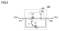
- FIG. 2 is an equivalent circuit diagram of the filter device;
- FIG. It is a figure explaining the reactance characteristic of a general LC parallel resonator.
- FIG. 4 is a diagram for explaining an inductive reactance required for resonance of an LC parallel resonator;
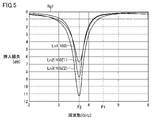
- FIG. 5 is a diagram showing an example of the insertion loss of the filter device according to Embodiment 1 and the insertion loss of the filter device of the comparative example;
- FIG. 6 is an enlarged view along the vertical axis of the area shown in FIG. 5;
- FIG. 5 is a diagram showing an example of the insertion loss of the filter device according to Embodiment 1 and the insertion loss of the filter device of the comparative example;
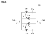
- FIG. 4 is a diagram showing a circuit configuration in which LC parallel resonators are connected in parallel;
- FIG. 9 is an exploded view of a filter device that implements the circuit configuration shown in FIG. 8;
- FIG. 10 is a diagram showing the configuration of an antenna module according to Embodiment 2;
- FIG. 10 is a diagram showing an example of the antenna device and return loss in Embodiment 2 and the return loss of an antenna device of a comparative example; It is a figure which shows the isolation characteristic between antenna devices. It is a figure which shows the radiation efficiency of an antenna device.
- FIG. 10 is a diagram showing combined reactance characteristics of an LC parallel resonator according to Embodiment 2;
- FIG. 10 is a diagram showing insertion loss of the filter device according to Embodiment 2;
- FIG. 10 is a diagram showing the insertion loss of the antenna in Embodiment 2;
- FIG. 10 is a diagram showing an example of insertion loss of an antenna device in a modified example of Embodiment 2 and insertion loss of an antenna device of a comparative example;
- FIG. 10 is a diagram showing an example of the radiation efficiency of an antenna device in a modified example of Embodiment 2 and the radiation efficiency of an antenna device in a comparative example;
- FIG. 4 is a diagram showing the radiation efficiency of an antenna when it is an inverted F-type antenna; It is an external view of the antenna module which is a loop antenna.
- FIG. 4 is a diagram showing the radiation efficiency of an antenna when it is a loop antenna; 1 is an external view of an antenna module that is a patch antenna;
- FIG. 4 is a diagram showing radiation efficiency of an antenna when it is a patch antenna;
- FIG. 1 is a diagram showing the configuration of an antenna device 150 according to Embodiment 1.
- Antenna device 150 includes a feeding circuit RF1, a filter device 100, and an antenna 155.
- the antenna device 150 is installed in, for example, a mobile terminal such as a mobile phone, a smart phone, or a tablet, or a communication device such as a personal computer having a communication function.
- the feeding circuit RF1 supplies the antenna 155 with a high-frequency signal in the frequency band of the f1 band.
- the antenna 155 can radiate into the air, as radio waves, a high-frequency signal in the f1 band supplied from the feeder circuit RF1.
- the frequency band of the f1 band is, for example, the 5 GHz band (5.15-5.7 GHz) of Wi-Fi (registered trademark).
- Antenna 155 is, for example, a monopole antenna.
- the filter device 100 is a trap filter that prevents passage of high-frequency signals in a specific frequency band and attenuates them.
- Filter device 100 is also referred to as a band-eliminating filter.
- the filter device 100 according to the first embodiment is configured to attenuate high frequency signals in the f2 frequency band.
- the frequency band of the f2 band includes 5G-NR (New Radio) n77 (3.3-4.2 GHz) and n78 (3.3-3.8 GHz).
- the f1 band and the f2 band are adjacent frequency bands. Whether or not frequency bands are adjacent is determined, for example, using a bandwidth and a center frequency for that bandwidth.
- the f1 band is the passband and the f2 band is the attenuation band.
- the antenna device 150 includes transmission lines TL1, TL2, and TL3.
- the transmission line TL1 and the transmission line TL2 are electrically connected at the connection point SP.
- the transmission line TL1 (first transmission line) is a transmission line from the connection point SP to the feeder circuit RF1 or another component arranged on the feeder circuit RF1 side. That is, one end of the transmission line TL1 is connected to the feeder circuit RF1 or another component arranged on the feeder circuit RF1 side, and the other end of the transmission line TL1 is connected to the transmission line TL2 (second transmission line) at the connection point SP.
- the transmission line TL2 is a transmission line from the connection point SP to the filter device 100. That is, one end of the transmission line TL2 is connected to the transmission line TL1 at the connection point SP, and the other end of the transmission line TL2 is connected to the filter device 100.
- FIG. A transmission line TL 3 (third transmission line) is a transmission line from the filter device 100 to the antenna 155 . That is, one end of the transmission line TL3 is connected to the filter device 100 and the other end of the transmission line TL3 is connected to the antenna 155.
- FIG. 1 describes an example in which the filter device 100 is connected to the antenna 155, the filter device 100 may be connected to a power amplifier or the like.
- FIG. 2 is an equivalent circuit diagram of the filter device 100.
- Terminal P1 is a terminal for connecting filter device 100 to transmission line TL2.
- Terminal P2 is a terminal for connecting filter device 100 to transmission line TL3 on the antenna 155 side.
- the terminal P1 When the feed circuit RF1 supplies a high frequency signal to the antenna 155 through the filter device 100, the terminal P1 becomes an input terminal and the terminal P2 becomes an output terminal.
- the terminal P1 When the high-frequency signal received by the antenna 155 is transmitted to the circuit on the power supply circuit RF1 side through the filter device 100, the terminal P1 becomes an output terminal and the terminal P2 becomes an input terminal.
- Filter device 100 does not have a ground electrode and is constructed as an integrated component.
- the filter device 100 includes an inductor L1, an inductor L2, and a capacitor C1.
- the LC series resonator RS is an LC series resonator formed by connecting an inductor L2 and a capacitor C1 in series.
- An LC series resonator RS is arranged between terminals P1 and P2.
- the inductor L1 is connected in parallel with the LC series resonator RS. That is, inductor L1 is also arranged between terminal P1 and terminal P2.
- the LC parallel resonator RP is an LC parallel resonator formed by connecting the inductor L1 and the LC series resonator RS in parallel.
- the inductor L1 and the inductor L2 are magnetically coupled in a direction that strengthens the magnetic fluxes. Thereby, a mutual inductance M is generated between the inductor L1 and the inductor L2.
- Magnetic coupling between inductor L1 and inductor L2 is additive coupling. That is, when current flows from the terminal P1 to the terminal P2 in FIG. 2, the direction of the magnetic field generated by the inductor L1 is opposite to the direction of the magnetic field generated by the inductor L2.
- the inductance of inductor L1 is smaller than the inductance of inductor L2.
- Filter device 100 uses LC parallel resonator RP and LC series resonator RS shown in FIG.
- the filter device 100 may also include other components such as impedance matching circuits and switches.
- a general LC parallel resonator means an LC parallel resonator in which only an inductor and a capacitor are connected in parallel, rather than an LC parallel resonator RP including an LC series resonator RS as shown in FIG. .
- FIG. 3 is a diagram for explaining the reactance characteristics of general LC parallel resonators 300M,N.
- lines LnM1, LnM2, LnN1, LnN2 representing reactances in the two LC parallel resonators 300M and 300N are shown.
- the horizontal axis indicates the frequency of the high frequency signal, and the vertical axis indicates the reactance value of the LC parallel resonator.
- the LC parallel resonator 300M and the LC parallel resonator 300N are examples of general LC parallel resonators in which an inductor and a capacitor are connected in parallel. have different inductance values of inductors and different capacitance values of capacitors.
- the inductance of the inductor of the LC parallel resonator 300N is 1 nH, and the capacitance of the capacitor is 3 pF.
- the inductance of the inductor of the LC parallel resonator 300M is 3 nH and the capacitance of the capacitor is 1 pF.
- Lines LnN1 and LnN2 represent the reactance of the LC parallel resonator 300N.
- Lines LnM1 and LnM2 represent the reactance of the LC parallel resonator 300M.
- the LC parallel resonator 300N resonates in a frequency band between the frequency at which the absolute value of the line LnN1 converges to infinity and the frequency at which the absolute value of the line LnN2 converges to infinity. As a result, the frequency band becomes the attenuation band d2 in the LC parallel resonator 300N.
- the LC parallel resonator 300M resonates in a frequency band between the frequency at which the absolute value of the line LnM1 converges to infinity and the frequency at which the absolute value of the line LnM2 converges to infinity. As a result, the frequency band becomes the attenuation band d1 in the LC parallel resonator 300M.
- LC parallel resonators 300M and 300N are configured such that attenuation band d1 and attenuation band d2 are included in the frequency band of f2 band.
- the attenuation band d2 of the LC parallel resonator 300N whose inductor inductance is smaller than that of the LC parallel resonator 300M is narrower than the attenuation band d1 of the LC parallel resonator 300M. That is, in a general LC parallel resonator in which an inductor and a capacitor are connected in parallel, reducing the inductance of the parallel-connected inductor narrows the attenuation band and improves steepness.
- the inductor L1 in the LC parallel resonator RP shown in FIG. 2 corresponds to the inductor in the general LC parallel resonators 300M, N described in FIG. That is, in the filter device 100 having the equivalent circuit configuration shown in FIG. 2, the attenuation band of the filter device 100 can be narrowed by reducing the inductor L1 corresponding to the inductor of a general LC parallel resonator. can.
- FIG. 4 is a diagram for explaining the inductive reactance required for resonance of the LC parallel resonator RP.
- the horizontal axis indicates the frequency of the high frequency signal, and the vertical axis indicates the reactance value.
- Filter device 100 is an example of a filter device having the equivalent circuit shown in FIG. As shown in FIG. 2, in the filter device 100, an additive magnetic coupling is performed between the inductor L1 and the inductor L2.
- the filter device 100Q of the comparative example is a filter device in which magnetic coupling is not made between the inductors L1 and L2. Filter device 100Q has the same configuration as filter device 100, except that magnetic coupling is not performed between inductor L1 and inductor L2.
- a line LnP indicates the capacitive reactance of the LC series resonator RS in the filter device 100 .
- Line LnQ represents the capacitive reactance of the LC series resonator RS in filter device 100Q.
- the capacitive reactance rc3 of the LC series resonator RS in the filter device 100 is higher than the capacitive reactance rc4 of the LC series resonator RS in the filter device 100Q. This is because the mutual inductance M corresponding to the coupling coefficient k is generated by the magnetic coupling between the inductors L1 and L2.
- the capacitive reactance values of the LC series resonators RS in the filter devices 100 and 100Q are both 0 in the f1 band. That is, a high-frequency signal having a frequency belonging to the f1 band passes through LC series resonators RS in filter device 100 and filter device 100Q. As a result, filter device 100 and filter device 100Q can pass high-frequency signals in the f1 band, which is the passband.
- a dashed line LnQp indicates the inductive reactance of the inductor L1 in the filter device 100Q.
- the value of the inductive reactance of the inductor L1 in order to resonate the LC parallel resonator RP in the f2 band, the value of the inductive reactance of the inductor L1 must be the inductive reactance rc1 shown in FIG. That is, the absolute value of the inductive reactance rc1 is the same as the absolute value of the capacitive reactance rc4.
- a dashed line LnPp indicates the inductive reactance of inductor L1 of filter device 100 .
- the value of the inductive reactance of the inductor L1 must be the inductive reactance rc2 shown in FIG. That is, the absolute value of the inductive reactance rc2 is the same as the absolute value of the capacitive reactance rc3.
- the inductive reactance rc2 required to resonate the LC parallel resonator RP in the filter device 100 is smaller than the inductive reactance rc1. This is because the mutual inductance M results in the capacitive reactance rc3 being higher than the capacitive reactance rc4.
- the inductive reactance rc2 itself also reduces the value of the inductor L1 because the mutual inductance M is added to the inductance of the inductor L1.
- inductor L1 and inductor L2 are magnetically coupled with added polarity, so that the inductance of inductor L1 can be reduced compared to filter device 100Q.
- depolarizing magnetic coupling may be performed instead of additive coupling if the inductance of inductor L1 is smaller than that of inductor L2.
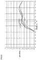
- FIG. 5 is a diagram showing an example of the insertion loss of filter device 100 in Embodiment 1 and the insertion loss of filter devices 100Z1 and 100Z2 of comparative examples.
- FIG. 5 shows lines Ln1 to Ln3 indicating insertion losses of filter device 100 according to the first embodiment and filter devices 100Z1 and 100Z2 of the comparative example.
- the horizontal axis indicates the frequency of the high frequency signal
- the vertical axis indicates the insertion loss of the high frequency signal.
- the insertion loss is the ratio of the power that is output to the power that is input to the filter device 100 . If the insertion loss is large, high-frequency signals are less likely to pass through the filter device, and if the insertion loss is small, high-frequency signals are more likely to pass through the filter device.
- a line Ln1 indicates the waveform of the insertion loss of the filter device 100 according to the first embodiment.
- a line Ln2 indicates the waveform of the insertion loss of the filter device 100Z1 in the comparative example.
- a line Ln3 indicates the waveform of the insertion loss of the filter device 100Z2 in the comparative example.
- Each of filter device 100, filter device 100Z1, and filter device 100Z2 is an example of a filter device having a configuration similar to that of LC parallel resonator RP shown in FIG. 2, but differs in the following points.
- inductor L1 has an inductance of 0.775 nH
- inductor L2 has an inductance of 0.997 nH
- capacitor C1 has a capacitance of 0.885 pF. Additive magnetic coupling.
- inductor L1 has an inductance of 1.195 nH
- inductor L2 has an inductance of 1.417 nH
- capacitor C1 has a capacitance of 0.885 pF
- inductor L1 and inductor L2 are depolarized. magnetic coupling.
- the inductance of inductor L1 is 0.997 nH
- the inductance of inductor L2 is 0.775 nH
- the capacitance of capacitor C1 is 0.885 pF
- inductor L1 and inductor L2 have additive polarity. magnetic coupling.
- the filter device 100Z1 of the comparative example differs from the filter device 100 of the first embodiment in that the magnetic coupling between the inductors L1 and L2 is depolarizing coupling.
- Filter device 100Z2 of the comparative example differs from filter device 100 of the first embodiment in that the inductance of inductor L1 is greater than the inductance of inductor L2.
- the inductances of the inductors L1 and L2 and the capacitance of the capacitor C1 are not limited to the above values. Also, the inductance values of the inductors L1 and L2 and the capacitance value of the capacitor C1 of each filter device include stray capacitance and stray inductance.
- the frequency at which each line Ln1 to Ln3 attenuates is the frequency F2. That is, the frequency F2 is the resonance frequency of the LC parallel resonator RP. Moreover, the frequency F2 is a frequency belonging to the f2 band, which is an attenuation band. Therefore, as shown in FIG. 5, in any one of the filter devices 100, 100Z1, and 100Z2, the insertion loss is the largest at the frequency F2 in the f2 band. On the other hand, the frequency F1 belongs to the f1 band, which is the passband. The insertion loss of frequencies belonging to the f1 band in filter devices 100, 100Z1, and 100Z2 will be described below with reference to FIG.
- the frequency F2 is treated as an arbitrary frequency belonging to the f2 band
- the frequency F1 is treated as an arbitrary frequency belonging to the f1 band. That is, the frequency F2 may be a frequency belonging to the f2 band, and the frequency F1 may be a frequency belonging to the f1 band.
- FIG. 6 is an enlarged view along the vertical axis of region Rg1 shown in FIG.
- FIG. 6 shows a waveform in which the vertical axis (insertion loss) direction of the region Rg1 shown in FIG. 5 is enlarged.
- the ratios in the horizontal axis (frequency) direction in FIG. 6 are the same as those in FIG. 5, and only the ratios in the vertical axis (insertion loss) direction are enlarged.
- the insertion loss when a high-frequency signal of frequency F1 passes is 0.418 dB for line LN1, 0.468 dB for line LN2, and 0.773 dB for line LN3.
- the insertion loss of the filter device 100 according to the first embodiment is the smallest among the filter device 100 according to the first embodiment and the filter devices 100Z1 and 100Z2 according to the comparative examples. That is, filter device 100 according to Embodiment 1 uses the f2 band as an attenuation band, as in filter devices 100Z1 and Z2, while the high-frequency signal of frequency F1 belonging to the f1 band, which is the passband, is higher than that of filter devices 100Z1 and Z2. is the easiest to pass.
- the inductance of the inductor L1 is smaller than the inductance of the inductor L2.
- the insertion loss in the f1 band can be made smaller than in the comparative example. That is, in the filter device 100 of Embodiment 1, it is possible to suppress loss that occurs when passing a high frequency signal in the f1 band.
- the inductance of the inductor L1 can be made smaller, so that the steepness of the attenuation band can be further improved. becomes possible.
- FIG. 7 is a diagram showing an example of the insertion loss of the filter device 100 according to Embodiment 1 and the insertion loss of the filter device Z3 of the comparative example.
- FIG. 7 shows lines Ln4 and Ln5 indicating the insertion loss of filter device 100 according to the first embodiment and the filter device of the comparative example.
- the horizontal axis indicates the frequency of the high frequency signal
- the vertical axis indicates the insertion loss of the high frequency signal.
- filter device 100 and LC parallel resonator RP of filter device 100Z3 are adjusted so that resonance frequency F2 is 4.35 GHz.
- a line Ln4 indicates the waveform of the insertion loss of the filter device 100 according to the first embodiment.
- a line Ln5 indicates the waveform of the insertion loss of the filter device 100Z3 in the comparative example.
- Filter device 100 and filter device 100Z3 have the same configuration, but filter device 100Z3 is connected to 50 ⁇ transmission line TL2 and 50 ⁇ transmission line TL3.
- the filter device 100 is connected between the 5 ⁇ transmission line TL2 and the 5 ⁇ transmission line TL3.
- the ratio between the characteristic impedance of the transmission line and the characteristic impedance of filter device 100 is increased by being connected to transmission lines TL1 and TL2 whose characteristic impedance is lower than 50 ⁇ .
- the characteristic impedances of the transmission line TL2 and the transmission line TL3 may be other values as long as they are less than 50 ⁇ .
- FIG. 8 is a diagram showing a circuit configuration in which LC parallel resonators RP are connected in parallel.
- FIG. 9 is an exploded view of filter device 100 formed as an integral element.
- FIG. 8 shows a filter device 100 having a circuit configuration that realizes the equivalent circuit shown in FIG. 2 by connecting the LC parallel resonators RP shown in FIG. 2 in parallel.
- Inductor L1a and inductor L1b in FIG. 8 function as inductor L1 in FIG.
- inductor L2a and inductor L2b in FIG. 8 function as inductor L2 in FIG.
- Capacitor C1a and capacitor C1b in FIG. 8 function as capacitor C1 in FIG.
- the inductor L2a and the inductor L1a are magnetically coupled with additive polarity.
- the inductor L2b and the inductor L1b are magnetically coupled with additive polarity.
- the inductor L2 shown in FIG. 2 includes an inductor L2a (fifth inductor) and an inductor L2b (sixth inductor) arranged in a laminate.
- capacitor C1 shown in FIG. 2 includes capacitor C1a and capacitor C1b arranged in a stack.
- the filter device 100 is constructed by stacking ten dielectric layers Ly1 to Ly10. That is, the filter device 100 includes a laminated body in which dielectric layers Ly1 to Ly10 are laminated.
- FIG. 9 shows a state in which each of the dielectric layers Ly1 to Ly10 is viewed from above.
- the shaded area means an electrode for transmitting a high frequency signal
- the circular shape means the end of a via connecting each dielectric layer.
- Terminals in1, in2, in3, and in4 are provided on the dielectric layers Ly3, Ly5, Ly6, and Ly8, respectively. Each of terminals in1, in2, in3 and in4 is connected to terminal P1 in FIG. Terminals out1, out2, out3, and out4 are provided on the dielectric layers Ly2, Ly4, Ly7, and Ly9, respectively. Each of terminals out1, out2, out3 and out4 is connected to terminal P2 in FIG.
- winding-shaped electrodes included in the dielectric layer Ly1, the dielectric layer Ly2, and the dielectric layer Ly3 form an inductor L2a.
- Plate-shaped electrodes included in the dielectric layer Ly1, the dielectric layer Ly2, the dielectric layer Ly3, and the dielectric layer Ly4 form a capacitor C1a.
- the winding-shaped electrodes included in the dielectric layers Ly4 and Ly5 form an inductor L1a.
- a wire-shaped electrode included in the dielectric layers Ly6 and Ly7 forms an inductor L1b.
- the winding-shaped electrodes included in the dielectric layers Ly8, Ly9, and Ly10 form an inductor L2b.
- Plate-shaped electrodes included in the dielectric layer Ly7, the dielectric layer Ly8, the dielectric layer Ly9, and the dielectric layer Ly10 form a capacitor C1b.
- the steepness of the attenuation band is improved by reducing the inductance of the inductor L1.
- the inductor L1 and the inductor L2 are magnetically coupled with additive polarity. This produces a mutual inductance M, and the inductance of inductor L1 becomes smaller.
- inductor L1a and inductor L1b are arranged in parallel. Specifically, the inductor L1a is formed by the electrodes of the dielectric layers Ly4 and Ly5, and the inductor L1b is formed by the electrodes of the dielectric layers Ly6 and Ly7 adjacent to the dielectric layers Ly4 and Ly5.
- the mutual inductance M due to the additive magnetic coupling between the inductors L1a and L2a can be increased without increasing the combined inductance of the inductors L1a and L1b. can be done.
- Magnetic coupling between inductor L1a and inductor L1b can increase the inductance of inductor L1a and inductor L1b.
- the filter device 100 of FIG. 9 is configured such that the winding direction of the inductor L1a and the winding direction of the inductor L1b are different. Specifically, as indicated by an arrow Ar1, the winding electrode of the dielectric layer Ly5 turns counterclockwise from the terminal in2. After that, the winding electrodes of the dielectric layer Ly5 are connected to the winding electrodes of the dielectric layer Ly4 through vias. The winding electrode of dielectric layer Ly4 turns counterclockwise further from the end of the via, as indicated by arrow Ar2. That is, as indicated by arrows Ar1 and Ar2, the winding direction of the inductor L1a when the laminate is planarized is counterclockwise (counterclockwise).
- the winding electrode of the dielectric layer Ly6 turns clockwise from the terminal in3.
- the winding electrodes of the dielectric layer Ly6 are connected to the winding electrodes of the dielectric layer Ly7 through vias.
- the winding electrode of dielectric layer Ly7 turns clockwise further from the end of the via, as indicated by arrow Ar4. That is, as indicated by arrows Ar3 and Ar4, the winding direction of the inductor L1b when the laminate is planarized is clockwise (rightward).
- the winding directions of the inductors L1a and L1b are opposite to each other, which reduces the overlap between the inductors L1a and L1b in plan view.
- the magnetic coupling between the inductor L1a and the inductor L1b is reduced, and the inductance of the inductor L1a and the inductor L1b is prevented from increasing. can be placed in adjacent dielectric layers.
- the area where the winding forming the inductor L2a in the multilayer body Ly3 overlaps the winding forming the inductor L1a in the multilayer body Ly4 is the same as that of the winding forming the inductor L1a in the multilayer body Ly5. is greater than the area overlapping the winding forming inductor L2a in .
- the coupling coefficient of the magnetic coupling between inductor L2a and inductor L1a can be increased, and the inductance of inductor L1a can be further reduced.
- the coupling coefficient of the magnetic coupling between inductor L2b and inductor L1b can be increased, and the inductance of inductor L1b can be made smaller.
- the inductors L1a, L1b, L2a, and L2b are arranged so as not to overlap the capacitors C1a and C1b when the laminates Ly1 to Ly10 are viewed from above. .
- the magnetic flux generated by the magnetic coupling between the inductors L1a and L2a and the magnetic flux generated by the magnetic coupling between the inductors L1b and L2b can be increased without interrupting the magnetic flux generated by the magnetic coupling between the inductors L1a and L2b. You can prevent it from increasing.
- the filter device 100 of the first embodiment may have a configuration including any one of the dielectric layers Ly1 to Ly5 or Ly6 to Ly10 of the laminate in FIG.
- Embodiment 2 In Embodiment 1 above, the antenna device 150 having the antenna 155 has been described. In Embodiment 2, antenna module 200 including antenna device 160 in addition to antenna device 150 in Embodiment 1 will be described. In antenna module 200 of the second embodiment, description of the configuration overlapping with antenna device 150 of the first embodiment will not be repeated.
- FIG. 10 is a diagram showing the configuration of antenna module 200 according to the second embodiment.
- Antenna module 200 includes antenna device 150 and antenna device 160 .
- Antenna device 160 includes a feeding circuit RF2 and an antenna 165 .
- the antenna module 200 is installed in, for example, a mobile terminal such as a mobile phone, a smart phone, or a tablet, or a communication device such as a personal computer having a communication function.
- the feeding circuit RF1 supplies the antenna 155 with high-frequency signals in the frequency bands of the f1 band and the f3 band.
- Antenna 155 can radiate into the air, as radio waves, high-frequency signals in the f1 band and f3 band supplied from feeder circuit RF1.
- the frequency band of the f1 band is, for example, the Wi-Fi 5 GHz band (5.15-5.7 GHz).
- the frequency band of the f3 band is, for example, the Wi-Fi 2 GHz band (2.4-2.48 GHz).
- the filter device 100 is configured to attenuate high frequency signals in the f2 frequency band.
- the frequency band of the f2 band is, for example, a band such as n77 (3.3-4.2 GHz) of 5G-NR.
- the f2 band is not limited to n77 (3.3-4.2 GHz), but includes n78 (3.3-3.8 GHz) and n79 (4.4-4.9 GHz) in addition to n77. good too.
- the f1 and f3 bands are passbands, and the f2 band is an attenuation band.
- the f2 band is a frequency band between the f1 band and the f3 band.
- the f2 band frequency band is lower than the f1 band frequency band.
- the frequency band of the f3 band is lower than the frequency band of the f2 band.
- the f1 band is the highest frequency band and the f3 band is the lowest frequency band.
- the relationship among the f1 band, f2 band, and f3 band is such that the f1 band, f2 band, and f3 band become lower in the order of f1 band, f2 band, and f3 band, each of the f1 band, f2 band, and f3 band is a different frequency band.
- the resonance frequency F2 of the LC parallel resonator RP of the filter device 100 according to the second embodiment is adjusted to be 3.8 GHz, which is near the median value of the f2 band according to the second embodiment.
- the feeding circuit RF2 supplies the antenna 165 with a high-frequency signal in the frequency band of the f2 band.
- the antenna 165 can radiate into the air the f2-band high-frequency signal supplied from the feeder circuit RF2 as radio waves.
- the filter device 100 is provided to remove the f2 band high-frequency signal, which may become noise in the antenna device 150, by increasing the insertion loss due to parallel resonance.
- the antenna 155 and the antenna 165 are mounted on the same substrate 170. Although the antennas 155 and 165 are provided on the same substrate 170 in FIG. 10, they may be provided on different substrates as long as they are provided in the same antenna module 200. FIG. Further, in the second embodiment, the power feeding circuit RF1 may not supply the high frequency signal in the f3 band, but may supply only the high frequency signal in the f1 band.
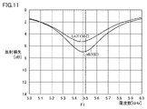
- FIG. 11 is a diagram showing an example of the return loss of the antenna device 150 according to Embodiment 2 and the return loss of the antenna device 150Z of the comparative example.
- the horizontal axis indicates the frequency of the high frequency signal, and the vertical axis indicates the return loss of the high frequency signal.
- the reflection loss indicates the ratio of the reflected power to the power supplied from the feeding circuit RF1 of the antenna device 150. FIG. That is, when power is radiated from the antenna, reflection loss also increases.
- a line Ln6 shows the waveform of the return loss of the antenna device 150 in the second embodiment.
- a line Ln7 indicates the waveform of the return loss of the antenna device 150Z in the comparative example.
- the antenna device 150Z has a configuration obtained by removing the filter device 100 from the antenna device 150 shown in FIG. That is, the antenna device 150 of the second embodiment and the antenna device 150Z of the comparative example differ in whether or not the filter device 100 is provided.
- the return loss of the antenna device 150 according to the second embodiment including the filter device 100 is as compared to that of the antenna device 150Z of the comparative example. growing. That is, by providing the filter device 100, the antenna characteristics of the antenna device 150 are improved as compared with the antenna device 150Z of the comparative example. Lines Ln7 and Ln6 both attenuate at frequency F1. In other words, between the antenna device 150 and the antenna device 150Z, the series resonance of the filter device 100 does not cause a shift in impedance frequency, and matching can be maintained. In other words, impedance matching does not deteriorate depending on whether or not the filter device 100 is provided. Therefore, in the antenna module 200 of Embodiment 2, the filter device 100 can be mounted on the antenna device 150 without re-matching the deterioration of the impedance.
- FIG. 12 is a diagram showing isolation characteristics between the antenna device 150 and the antenna device 160.
- FIG. The horizontal axis indicates the frequency of the high frequency signal, and the vertical axis indicates the isolation of the high frequency signal. That is, the isolation is the ratio of the power received by the feeder circuit RF2 of the antenna device 160 via the antenna to the power input from the feeder circuit RF1 of the antenna device 150 .
- a line Ln8 indicates the isolation between the antenna device 150 and the antenna device 160 of the antenna module 200 in the second embodiment.
- a line Ln9 indicates the isolation between the antenna device 150 and the antenna device 160 of the antenna module 200Z in the comparative example.
- the antenna module 200Z has a configuration obtained by removing the filter device 100 from the antenna module 200 of FIG. That is, the antenna module 200 of the second embodiment and the antenna module 200Z of the comparative example differ in whether or not the filter device 100 is provided.
- the antenna module 200 of Embodiment 2 has an isolation of 15 dB or more greater than that of the antenna module 200Z of the comparative example. That is, in the second embodiment, filter device 100 attenuates frequencies in the f2 band, thereby improving the isolation of antenna devices 150 and 160 compared to the comparative example.
- FIG. 13 is a diagram showing the radiation efficiency of the antenna device 160.
- FIG. The horizontal axis indicates the frequency of the high frequency signal, and the vertical axis indicates the radiation efficiency of the antenna device 160 .
- a line Ln10 indicates the radiation efficiency of the antenna device 160 of the antenna module 200 in the second embodiment.
- a line Ln11 indicates the radiation efficiency of the antenna device 160 of the antenna module 200Z in the comparative example.
- the radiation efficiency means the ratio of the power radiated from the antenna to the power supplied from the feeding circuit. That is, in FIG. 13, the power radiated from the antenna increases toward the top of the graph for the same supplied power.
- the radiation efficiency of the antenna module 200 of Embodiment 2 is improved by about 4.5 dB compared to the antenna module 200Z of the comparative example. That is, in the second embodiment, the antenna device 150 is provided with the filter device 100, so that the radiation efficiency of the antenna device 160 can be improved more than the comparative example.
- the filter device 100Z2 of the comparative example differs from the filter device 100 of the second embodiment in that the inductance of the inductor L1 is larger than the inductance of the inductor L2.
- FIG. 14 is a diagram showing synthetic reactance characteristics of the LC parallel resonator RP according to the second embodiment.
- the horizontal axis indicates the frequency of the high-frequency signal
- the vertical axis indicates the synthetic reactance value of the LC parallel resonator RP.
- a line Ln15 indicates the value of the combined reactance of the LC parallel resonator RP of the filter device 100 according to the second embodiment.
- a line Ln14 indicates the value of the combined reactance of the LC parallel resonator RP in the filter device 100Z2 when the filter device 100Z2 of the comparative example is applied.
- the value of the combined reactance at frequency F1 in the f1 band and frequency F3 in the f3 band, which are the passbands, is higher than that of the comparative example. become smaller.
- high-frequency signals of frequencies F1 and F3 included in the passband pass through filter device 100 more easily than through filter device 100Z2.
- the frequency F3 is treated as any frequency belonging to the f3 band. That is, the frequency F3 may be any frequency belonging to the f3 band.
- FIG. 15 is a diagram showing the insertion loss of the filter device 100 according to the second embodiment.
- Line Ln13 indicates the insertion loss of filter device 100 of antenna module 200 in the second embodiment.
- a line Ln14 indicates the insertion loss of the filter device 100Z2 when the filter device 100Z2 in the comparative example is applied to the second embodiment.
- the combined reactance is small at the frequency F1 of the f1 band and the frequency F3 of the f3 band, which are the passbands, as shown in FIG.
- the insertion loss of the filter device 100 is smaller than that of the filter device 100Z2 of the comparative example.
- filter device 100 since the inductance of inductor L1 is smaller than the inductance of inductor L2, filter device 100 according to the second embodiment can more easily pass high-frequency signals having frequencies F1 and F3 in passbands closer to the attenuation band than in the comparative example. Become.
- the f2 band is used as the attenuation band by setting the resonance frequency of the LC parallel resonator RP to the frequency F2 included in the f2 band.
- a high-frequency signal with a frequency F3 lower than the f2 band passes through the path in which the inductor L1 is arranged rather than the path of the LC series resonator RS. That is, when a high-frequency signal in the f3 band passes through, the path in which the inductor L1 is arranged becomes dominant.
- the inductance of inductor L1 is made smaller than the inductance of inductor L2 in order to narrow the attenuation band. This reduces the impedance when the frequency F3 passes through the inductor L1.
- the frequency F2 is efficiently radiated from the feeder circuit RF2, and the attenuation band is narrowed compared to the filter device 100Z2, thereby reducing the frequencies F1 and F3. Efficient radiation from the feeding circuit RF1 becomes possible.
- FIG. 16 is a diagram showing the insertion loss of the antenna 155 in Embodiment 2.
- FIG. A line Ln17 indicates the insertion loss of the antenna 155 of the antenna module 200 in the second embodiment.
- a line Ln18 indicates the insertion loss of the antenna 155Z in the comparative example.
- a line Ln19 indicates the insertion loss of the antenna 155Z1 in the comparative example.
- the antenna 155Z is an antenna obtained by removing the filter device 100 from the antenna device 150 shown in FIG.
- Antenna 155Z1 has a configuration including filter device 100Z2 instead of filter device 100 in antenna 155 shown in FIG.
- the frequency at which the line Ln17 has a large insertion loss approaches the frequency at which the line Ln18 has a large insertion loss rather than the frequency at which the line Ln19 has a large insertion loss. That is, impedance matching does not deteriorate when filter device 100 according to the second embodiment is mounted, compared to when filter device 100Z2 is mounted. Therefore, the filter device 100 of the second embodiment imposes less load on impedance matching when applied to the antenna module 200 than the filter device 100Z2 of the comparative example.
- the configuration designed so that the resonance frequency F2 of the LC parallel resonator RP of the filter device 100 is 3.8 GHz within the f2 band has been described.
- a filter device 100B designed such that the resonance frequency F2 of the LC parallel resonator RP is near the lower limit of the frequency band of the f2 band will be described.
- the frequency band of the f2 band is the 5G-NR n78 (3.3-3.8 GHz) band. That is, the resonance frequency F2 of the LC parallel resonator RP of the filter device 100B is 3.3 GHz.
- the filter device 100A is used as a comparative example for the filter device 100B.
- the resonance frequency F2 of the LC parallel resonator RP of the filter device 100A of the comparative example is adjusted to 3.5 GHz within the frequency band of the f2 band.
- filter device 100B according to the modification of the second embodiment descriptions of configurations that overlap those of the first and second embodiments will not be repeated.
- FIG. 17 is a diagram showing an example of the insertion loss of the filter device 100B in the modified example of the second embodiment and the insertion loss of the filter device 100A of the comparative example.
- 17 to 19 show frequency f2s indicating a frequency of 3.3 GHz near the lower limit of the f2 band, frequency f2c indicating a frequency of 3.5 GHz near the center of the f2 band, and frequency 3 near the upper limit of the f2 band.
- a frequency f2e representing 0.8 GHz is shown.
- antenna modules to which filter device 100A and filter device 100B are applied instead of filter device 100 in the second embodiment are referred to as antenna modules 250A and 250B, respectively.
- a line Ln20 shown in FIG. 17 indicates the insertion loss of the antenna device 150 of the antenna module 250B in the modified example of the second embodiment.
- a line Ln21 indicates the insertion loss of the antenna device 150 of the antenna module 250A of the comparative example in the modified example of the second embodiment.
- the resonance frequency F2 in the filter device 100B is designed to be the frequency f2s (3.3 GHz) near the lower limit of the n78 band. Note that the resonance frequency in filter device 100B may be, for example, 3.2 GHz or 3.4 GHz instead of 3.3 GHz.
- the resonance frequency F2 in the filter device 100A is designed to be the frequency f2c (3.5 GHz).
- FIG. 18 is a diagram showing an example of the radiation efficiency of the antenna device 150 in the modified example of Embodiment 2 and the radiation efficiency of the antenna device 150 in the comparative example.
- a line Ln22 shown in FIG. 18 indicates the radiation efficiency of the antenna device 150 of the antenna module 250B in the modified example of the second embodiment.
- a line Ln23 indicates the radiation efficiency of the antenna device 150 of the antenna module 250A of the comparative example in the modified example of the second embodiment.
- a line Ln24 indicates the radiation efficiency of the antenna device 150 of the antenna module 200Z of the comparative example in the modified example of the second embodiment.
- the antenna module 200Z has a configuration obtained by removing the filter device 100 from the antenna module 200 of FIG.
- the radiation efficiency of the antenna module 250A of the comparative example is lower than the radiation efficiency of the antenna module 200Z of the comparative example in the frequency band from the frequency f2s to the frequency f2c, especially around the frequency F2s.
- the radiation efficiency of antenna module 200B which is a modification of Embodiment 2
- the radiation efficiency of antenna module 200B is higher than that of antenna module 200Z of the comparative example in the frequency band from frequency F2s to frequency f2c. That is, the radiation efficiency of the antenna module 200B, which is a modification of the second embodiment, is higher than that of the antenna module 200Z of the comparative example in the entire f2 band (band from frequency f2s to frequency f2e).
- FIG. 19 is a diagram showing isolation characteristics between the antenna device 150 and the antenna device 160 in the modified example of the second embodiment.
- Line Ln25 indicates the isolation between antenna device 150 and antenna device 160 of antenna module 250B in the modification of the second embodiment.
- a line Ln26 indicates the isolation between the antenna device 150 and the antenna device 160 of the antenna module 200Z in the comparative example.
- the antenna module 250B has greater isolation than the antenna module 200Z of the comparative example. That is, in the modification of the second embodiment, filter device 100B attenuates frequencies in the f2 band, thereby improving the isolation of antenna devices 150 and 160 compared to the comparative example.
- the filter device 100B is adjusted so that the resonance frequency F2 is near the lower limit of the f2 band, which is the attenuation band.
- the resonance frequency F2 of the filter device 100B may be a frequency near the lower limit of the attenuation band, and may be a frequency lower than the lower limit of the attenuation band.
- FIG. 20 is an external view of the antenna module 201 in which the antenna 155 is an inverted F-type antenna. As shown in FIG. 20, antenna 155 is formed as an inverted F antenna. Antenna 165 is formed as a monopole antenna. As shown in FIG. 20, antenna 155 is connected to feeder circuit RF1 through filter device 100 .
- the antenna 155 which is an inverted F-type antenna, is branched from the path connecting to the feeding circuit RF1 and connected to the ground electrode GND.
- a branching point will be referred to as a branching point between a path connecting to the feeder circuit RF1 and a path connecting to the ground electrode GND.
- FIG. 21 is a diagram showing the radiation efficiency of the antenna 165 when the antenna 155 is an inverted F antenna.
- a line LnF1 indicates the radiation efficiency of the antenna 165 of the antenna module 201Z of the comparative example.
- a line LnF2 indicates the radiation efficiency of the antenna 165 of the antenna module 201 of the second embodiment.
- a line LnF3 indicates the radiation efficiency of the antenna 165 of the antenna module 201A of the first modification.
- a line LnF4 indicates the radiation efficiency of the antenna 165 of the antenna module 201B of the second modification.
- the antenna module 201Z of the comparative example does not include the filter device 100. That is, the antenna module 201Z has a configuration obtained by removing the filter device 100 from the antenna module 201 of FIG.
- the filter device 100 is not arranged on the path from the branch point to the feeder circuit RF1, but the filter device 100 is arranged on the path Rt from the branch point to the ground electrode GND. It has a configuration that
- Antenna module 201B of modification 2 has filter device 100 arranged on the path from the branch point to feed circuit RF1, and filter device 100 is arranged on path Rt from the branch point to ground electrode GND. It has a configuration that That is, the antenna device 150 of the antenna module 200B of Modification 2 includes two filter devices 100 .
- the radiation efficiency of the antenna 165 in the antenna module 201Z of the comparative example without the filter device 100 is the lowest. That is, in Embodiment 2 and Modifications 1 and 2 to which an inverted F-type antenna is applied, the radiation efficiency of antenna 165 is improved over the comparative example by providing filter device 100 .
- FIG. 22 is an external view of the antenna module 202 in which the antenna 155 is a loop antenna.
- antenna 155 is formed as a loop antenna.
- Antenna 165 is formed as a monopole antenna.
- the antenna 155 which is a loop antenna, is also connected to the ground electrode GND via a path Rt different from the path connecting to the feeding circuit RF1.
- FIG. 23 is a diagram showing the radiation efficiency of the antenna 165 when the antenna 155 is a loop antenna.
- a line LnL1 indicates the radiation efficiency of the antenna 165 of the antenna module 202Z of the comparative example.
- a line LnL2 indicates the radiation efficiency of the antenna 165 of the antenna module 202 of the second embodiment.
- a line LnL3 indicates the radiation efficiency of the antenna 165 of the antenna module 202A of the first modification.
- a line LnL4 indicates the radiation efficiency of the antenna 165 of the antenna module 202B of the second modification.
- An antenna module 202Z of the comparative example has a configuration obtained by removing the filter device 100 from the antenna module 202 of FIG.
- the filter device 100 is arranged not on the path between the antenna 155 and the feeder circuit RF1, but on the path Rt between the antenna 155 and the ground electrode GND. It has a configuration that
- antenna module 202B of Modification 2 filter device 100 is arranged on the path from antenna 155 to feed circuit RF1, and filter device 100 is arranged on path Rt from antenna 155 to ground electrode GND. It has a configuration that
- the radiation efficiency of the antenna 165 in the antenna module 202Z of the comparative example without the filter device 100 is the lowest. That is, in Embodiment 2 and Modifications 1 and 2 to which the loop antenna is applied, the radiation efficiency of antenna 165 is improved by providing filter device 100 as compared to the comparative example.
- FIG. 24 is an external view of the antenna module 203 in which the antenna 155 is a patch antenna.
- antenna 155 is formed as a patch antenna.
- Antenna 165 is formed as a monopole antenna.
- antenna 155, which is a patch antenna is also connected to ground electrode GND via a path Rt different from the path connecting to feeder circuit RF1.
- FIG. 25 is a diagram showing the radiation efficiency of the antenna 165 when the antenna 155 is a patch antenna.
- a line LnP1 indicates the radiation efficiency of the antenna 165 of the antenna module 203Z of the comparative example.
- a line LnP2 indicates the radiation efficiency of the antenna 165 of the antenna module 203 of the second embodiment.
- a line LnP3 indicates the radiation efficiency of the antenna 165 of the antenna module 203A of the first modification.
- a line LnP4 indicates the radiation efficiency of the antenna 165 of the antenna module 203B of the second modification.
- An antenna module 203Z of the comparative example has a configuration obtained by removing the filter device 100 from the antenna module 203 of FIG.
- the filter device 100 is not arranged on the path between the antenna 155 and the feeder circuit RF1, but on the path Rt between the antenna 155 and the ground electrode GND.
- antenna module 203B of Modification 2 filter device 100 is arranged on the path from antenna 155 to feed circuit RF1, and filter device 100 is arranged on path Rt from antenna 155 to ground electrode GND. It has a configuration that
- the radiation efficiency of the antenna 165 in the antenna module 203Z of the comparative example without the filter device 100 is the lowest. That is, in Embodiment 2 and Modifications 1 and 2 to which the loop antenna is applied, the radiation efficiency of antenna 165 is improved by providing filter device 100 as compared to the comparative example.
- 100 filter device 150, 160 antenna device, 155, 165 antenna, 170 substrate, 200, 201, 202, 203, 250 antenna module, Ar1 to Ar4 arrows, C1a, C1b, C1 capacitors, F1 to F3, f2s, f2c, f2e Frequency, GND Ground electrode, L1, L1a, L1b, L2, L2b, L2a Inductor, Ly1 to Ly10 Dielectric layer, P1, P2, in1 to in4, out1 to out4 Terminals, RF1, RF2 Power supply circuit, RSLC series resonance device, RP LC parallel resonator, Rg1 region, SP connection point, TL1 to TL3 transmission line, d1, d2 attenuation band, M mutual inductance, rc1, rc2 inductive reactance, rc3, rc4 capacitive reactance, Rt path.
- Ar1 to Ar4 arrows C1a, C1b, C1 capacitors, F1
Landscapes
- Engineering & Computer Science (AREA)
- Power Engineering (AREA)
- Filters And Equalizers (AREA)
Priority Applications (3)
| Application Number | Priority Date | Filing Date | Title |
|---|---|---|---|
| JP2023531899A JP7593496B2 (ja) | 2021-07-02 | 2022-06-24 | フィルタ装置、アンテナ装置、およびアンテナモジュール |
| CN202280043010.6A CN117501624A (zh) | 2021-07-02 | 2022-06-24 | 滤波器装置、天线装置以及天线模块 |
| US18/391,743 US12494760B2 (en) | 2021-07-02 | 2023-12-21 | Filter device, antenna device, and antenna module |
Applications Claiming Priority (2)
| Application Number | Priority Date | Filing Date | Title |
|---|---|---|---|
| JP2021-111022 | 2021-07-02 | ||
| JP2021111022 | 2021-07-02 |
Related Child Applications (1)
| Application Number | Title | Priority Date | Filing Date |
|---|---|---|---|
| US18/391,743 Continuation US12494760B2 (en) | 2021-07-02 | 2023-12-21 | Filter device, antenna device, and antenna module |
Publications (1)
| Publication Number | Publication Date |
|---|---|
| WO2023276879A1 true WO2023276879A1 (ja) | 2023-01-05 |
Family
ID=84691401
Family Applications (1)
| Application Number | Title | Priority Date | Filing Date |
|---|---|---|---|
| PCT/JP2022/025295 Ceased WO2023276879A1 (ja) | 2021-07-02 | 2022-06-24 | フィルタ装置、アンテナ装置、およびアンテナモジュール |
Country Status (4)
| Country | Link |
|---|---|
| US (1) | US12494760B2 (https=) |
| JP (1) | JP7593496B2 (https=) |
| CN (1) | CN117501624A (https=) |
| WO (1) | WO2023276879A1 (https=) |
Cited By (1)
| Publication number | Priority date | Publication date | Assignee | Title |
|---|---|---|---|---|
| WO2025052762A1 (ja) * | 2023-09-07 | 2025-03-13 | 株式会社村田製作所 | フィルタ装置、アンテナ装置、およびアンテナモジュール |
Citations (4)
| Publication number | Priority date | Publication date | Assignee | Title |
|---|---|---|---|---|
| JP2004312741A (ja) * | 2003-04-03 | 2004-11-04 | Stmicroelectronics Sa | 一体型の二帯域インダクタンス及びその応用 |
| WO2005036741A1 (ja) * | 2003-10-14 | 2005-04-21 | Soc Corporation | ノイズ防止コイル回路 |
| WO2016167171A1 (ja) * | 2015-04-17 | 2016-10-20 | 株式会社村田製作所 | 共振回路、帯域阻止フィルタおよび帯域通過フィルタ |
| WO2018092453A1 (ja) * | 2016-11-18 | 2018-05-24 | 株式会社村田製作所 | 誘電体複合フィルタ、高周波モジュール、高周波フロントエンド回路、通信装置、及びMassive MIMOシステム |
Family Cites Families (1)
| Publication number | Priority date | Publication date | Assignee | Title |
|---|---|---|---|---|
| JP5573804B2 (ja) * | 2011-09-23 | 2014-08-20 | 株式会社村田製作所 | 帯域通過フィルタ |
-
2022
- 2022-06-24 WO PCT/JP2022/025295 patent/WO2023276879A1/ja not_active Ceased
- 2022-06-24 CN CN202280043010.6A patent/CN117501624A/zh active Pending
- 2022-06-24 JP JP2023531899A patent/JP7593496B2/ja active Active
-
2023
- 2023-12-21 US US18/391,743 patent/US12494760B2/en active Active
Patent Citations (4)
| Publication number | Priority date | Publication date | Assignee | Title |
|---|---|---|---|---|
| JP2004312741A (ja) * | 2003-04-03 | 2004-11-04 | Stmicroelectronics Sa | 一体型の二帯域インダクタンス及びその応用 |
| WO2005036741A1 (ja) * | 2003-10-14 | 2005-04-21 | Soc Corporation | ノイズ防止コイル回路 |
| WO2016167171A1 (ja) * | 2015-04-17 | 2016-10-20 | 株式会社村田製作所 | 共振回路、帯域阻止フィルタおよび帯域通過フィルタ |
| WO2018092453A1 (ja) * | 2016-11-18 | 2018-05-24 | 株式会社村田製作所 | 誘電体複合フィルタ、高周波モジュール、高周波フロントエンド回路、通信装置、及びMassive MIMOシステム |
Cited By (1)
| Publication number | Priority date | Publication date | Assignee | Title |
|---|---|---|---|---|
| WO2025052762A1 (ja) * | 2023-09-07 | 2025-03-13 | 株式会社村田製作所 | フィルタ装置、アンテナ装置、およびアンテナモジュール |
Also Published As
| Publication number | Publication date |
|---|---|
| JP7593496B2 (ja) | 2024-12-03 |
| US12494760B2 (en) | 2025-12-09 |
| US20240120897A1 (en) | 2024-04-11 |
| JPWO2023276879A1 (https=) | 2023-01-05 |
| CN117501624A (zh) | 2024-02-02 |
Similar Documents
| Publication | Publication Date | Title |
|---|---|---|
| JP5817795B2 (ja) | 高周波モジュール | |
| US9503051B2 (en) | High-frequency module having a matching element coupled to a connection unit | |
| JP6183461B2 (ja) | 高周波モジュール | |
| CN103348531B (zh) | 稳频电路、天线装置及通信终端装置 | |
| US9837976B2 (en) | Impedance converting circuit and communication terminal apparatus | |
| WO2015019794A1 (ja) | 高周波モジュール | |
| JP2017098998A (ja) | 電子機器 | |
| JPWO2015104882A1 (ja) | 高周波モジュール | |
| JP6760515B2 (ja) | 整合回路および通信装置 | |
| JP6662349B2 (ja) | 方向性結合器、高周波フロントエンドモジュール、および、通信機器 | |
| JP2012191596A (ja) | インピーダンス変換デバイス、アンテナ装置および通信端末装置 | |
| CN105453428B (zh) | 高频模块 | |
| JP6183462B2 (ja) | 高周波モジュール | |
| JP5804076B2 (ja) | Lcフィルタ回路及び高周波モジュール | |
| CN115917965B (zh) | 滤波器装置以及多路调制器 | |
| JP7601250B2 (ja) | フィルタ装置、アンテナ装置、およびアンテナモジュール | |
| JP7593496B2 (ja) | フィルタ装置、アンテナ装置、およびアンテナモジュール | |
| JP7622871B2 (ja) | フィルタ装置、アンテナ装置、およびアンテナモジュール | |
| KR20210081257A (ko) | 복합 필터 장치 및 밴드 패스 필터 | |
| JP7613586B2 (ja) | フィルタ装置およびそれを搭載した高周波フロントエンド回路 | |
| JP7613477B2 (ja) | フィルタ装置、ならびに、それを搭載した高周波フロントエンド回路およびダイプレクサ | |
| KR20180135114A (ko) | 고주파 스위치 모듈 | |
| JP2024144683A (ja) | フィルタモジュール及び電子機器 |
Legal Events
| Date | Code | Title | Description |
|---|---|---|---|
| 121 | Ep: the epo has been informed by wipo that ep was designated in this application |
Ref document number: 22833026 Country of ref document: EP Kind code of ref document: A1 |
|
| WWE | Wipo information: entry into national phase |
Ref document number: 2023531899 Country of ref document: JP |
|
| WWE | Wipo information: entry into national phase |
Ref document number: 202280043010.6 Country of ref document: CN |
|
| NENP | Non-entry into the national phase |
Ref country code: DE |
|
| 122 | Ep: pct application non-entry in european phase |
Ref document number: 22833026 Country of ref document: EP Kind code of ref document: A1 |