WO2023276879A1 - Filter device, antenna device, and antenna module - Google Patents
Filter device, antenna device, and antenna module Download PDFInfo
- Publication number
- WO2023276879A1 WO2023276879A1 PCT/JP2022/025295 JP2022025295W WO2023276879A1 WO 2023276879 A1 WO2023276879 A1 WO 2023276879A1 JP 2022025295 W JP2022025295 W JP 2022025295W WO 2023276879 A1 WO2023276879 A1 WO 2023276879A1
- Authority
- WO
- WIPO (PCT)
- Prior art keywords
- inductor
- antenna
- filter device
- band
- frequency
- Prior art date
Links
- 239000003990 capacitor Substances 0.000 claims abstract description 31
- 230000005540 biological transmission Effects 0.000 claims description 43
- 238000004804 winding Methods 0.000 claims description 19
- 239000000758 substrate Substances 0.000 claims description 5
- 230000000052 comparative effect Effects 0.000 description 67
- 238000003780 insertion Methods 0.000 description 50
- 230000037431 insertion Effects 0.000 description 50
- 230000005855 radiation Effects 0.000 description 44
- 238000010586 diagram Methods 0.000 description 38
- 230000008878 coupling Effects 0.000 description 27
- 238000010168 coupling process Methods 0.000 description 27
- 238000005859 coupling reaction Methods 0.000 description 27
- 238000012986 modification Methods 0.000 description 25
- 230000004048 modification Effects 0.000 description 25
- 230000001939 inductive effect Effects 0.000 description 14
- 238000002955 isolation Methods 0.000 description 14
- 230000001965 increasing effect Effects 0.000 description 11
- 239000000654 additive Substances 0.000 description 10
- 230000000996 additive effect Effects 0.000 description 10
- 230000004907 flux Effects 0.000 description 5
- 238000004891 communication Methods 0.000 description 4
- 230000005404 monopole Effects 0.000 description 4
- 238000000034 method Methods 0.000 description 3
- 230000002999 depolarising effect Effects 0.000 description 2
- 238000013459 approach Methods 0.000 description 1
- 230000006866 deterioration Effects 0.000 description 1
- 238000005516 engineering process Methods 0.000 description 1
- 101150068408 lnp1 gene Proteins 0.000 description 1
- 238000004725 rapid separation liquid chromatography Methods 0.000 description 1
- 238000004088 simulation Methods 0.000 description 1
Images


Classifications
-
- H—ELECTRICITY
- H01—ELECTRIC ELEMENTS
- H01Q—ANTENNAS, i.e. RADIO AERIALS
- H01Q1/00—Details of, or arrangements associated with, antennas
- H01Q1/52—Means for reducing coupling between antennas; Means for reducing coupling between an antenna and another structure
- H01Q1/521—Means for reducing coupling between antennas; Means for reducing coupling between an antenna and another structure reducing the coupling between adjacent antennas
-
- H—ELECTRICITY
- H03—ELECTRONIC CIRCUITRY
- H03H—IMPEDANCE NETWORKS, e.g. RESONANT CIRCUITS; RESONATORS
- H03H7/00—Multiple-port networks comprising only passive electrical elements as network components
- H03H7/01—Frequency selective two-port networks
- H03H7/0115—Frequency selective two-port networks comprising only inductors and capacitors
-
- H—ELECTRICITY
- H01—ELECTRIC ELEMENTS
- H01Q—ANTENNAS, i.e. RADIO AERIALS
- H01Q1/00—Details of, or arrangements associated with, antennas
- H01Q1/50—Structural association of antennas with earthing switches, lead-in devices or lightning protectors
-
- H—ELECTRICITY
- H01—ELECTRIC ELEMENTS
- H01Q—ANTENNAS, i.e. RADIO AERIALS
- H01Q21/00—Antenna arrays or systems
- H01Q21/28—Combinations of substantially independent non-interacting antenna units or systems
-
- H—ELECTRICITY
- H03—ELECTRONIC CIRCUITRY
- H03H—IMPEDANCE NETWORKS, e.g. RESONANT CIRCUITS; RESONATORS
- H03H5/00—One-port networks comprising only passive electrical elements as network components
- H03H5/02—One-port networks comprising only passive electrical elements as network components without voltage- or current-dependent elements
-
- H—ELECTRICITY
- H03—ELECTRONIC CIRCUITRY
- H03H—IMPEDANCE NETWORKS, e.g. RESONANT CIRCUITS; RESONATORS
- H03H7/00—Multiple-port networks comprising only passive electrical elements as network components
- H03H7/01—Frequency selective two-port networks
- H03H7/09—Filters comprising mutual inductance
-
- H—ELECTRICITY
- H03—ELECTRONIC CIRCUITRY
- H03H—IMPEDANCE NETWORKS, e.g. RESONANT CIRCUITS; RESONATORS
- H03H7/00—Multiple-port networks comprising only passive electrical elements as network components
- H03H7/01—Frequency selective two-port networks
- H03H7/17—Structural details of sub-circuits of frequency selective networks
- H03H7/1741—Comprising typical LC combinations, irrespective of presence and location of additional resistors
- H03H7/175—Series LC in series path
-
- H—ELECTRICITY
- H03—ELECTRONIC CIRCUITRY
- H03H—IMPEDANCE NETWORKS, e.g. RESONANT CIRCUITS; RESONATORS
- H03H7/00—Multiple-port networks comprising only passive electrical elements as network components
- H03H7/01—Frequency selective two-port networks
- H03H7/17—Structural details of sub-circuits of frequency selective networks
- H03H7/1741—Comprising typical LC combinations, irrespective of presence and location of additional resistors
- H03H7/1766—Parallel LC in series path
-
- H—ELECTRICITY
- H03—ELECTRONIC CIRCUITRY
- H03H—IMPEDANCE NETWORKS, e.g. RESONANT CIRCUITS; RESONATORS
- H03H7/00—Multiple-port networks comprising only passive electrical elements as network components
- H03H7/01—Frequency selective two-port networks
- H03H7/17—Structural details of sub-circuits of frequency selective networks
- H03H7/1741—Comprising typical LC combinations, irrespective of presence and location of additional resistors
- H03H7/1775—Parallel LC in shunt or branch path
-
- H—ELECTRICITY
- H03—ELECTRONIC CIRCUITRY
- H03H—IMPEDANCE NETWORKS, e.g. RESONANT CIRCUITS; RESONATORS
- H03H1/00—Constructional details of impedance networks whose electrical mode of operation is not specified or applicable to more than one type of network
- H03H2001/0021—Constructional details
- H03H2001/0085—Multilayer, e.g. LTCC, HTCC, green sheets
Definitions
- the present disclosure relates to a filter device, an antenna device, and an antenna module, and more specifically to technology for improving the steepness of an attenuation band.
- Patent Document 1 discloses a filter device in which a second inductor is connected in parallel to a series circuit composed of a first inductor and a first capacitor. The first inductor and the second inductor are coupled via a magnetic field in a direction in which magnetic fluxes are mutually strengthened.
- Patent Document 1 magnetic field coupling increases the effective inductance of the first inductor and the second inductor, so the inductance of each of the first inductor and the second inductor is reduced. Thereby, in the filter device of Patent Document 1, the resistance component of the parallel resonator can be reduced and the Q value can be improved.
- the present disclosure has been made to solve such problems, and its purpose is to improve the steepness of the attenuation band in a filter device for high-frequency signals, and pass high-frequency signals in a band close to the attenuation band. It is to suppress the loss that occurs in the case.
- a filter device has a first frequency band as a passband and a second frequency band as an attenuation band lower than the first frequency band.
- the filter device has a first terminal, a second terminal, a first inductor, and an LC series resonator.
- a first inductor is disposed between the first terminal and the second terminal.
- An LC series resonator is connected in parallel with the first inductor and includes a first capacitor and a second inductor.
- the first inductor and the second inductor are magnetically coupled to each other.
- the inductance of the first inductor is less than the inductance of the second inductor.
- the inductance of the first inductor is configured to be smaller than the inductance of the second inductor in the LC parallel resonator.
- FIG. 1 is a diagram showing a configuration of an antenna device according to Embodiment 1;
- FIG. 2 is an equivalent circuit diagram of the filter device;
- FIG. It is a figure explaining the reactance characteristic of a general LC parallel resonator.
- FIG. 4 is a diagram for explaining an inductive reactance required for resonance of an LC parallel resonator;
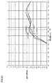
- FIG. 5 is a diagram showing an example of the insertion loss of the filter device according to Embodiment 1 and the insertion loss of the filter device of the comparative example;
- FIG. 6 is an enlarged view along the vertical axis of the area shown in FIG. 5;
- FIG. 5 is a diagram showing an example of the insertion loss of the filter device according to Embodiment 1 and the insertion loss of the filter device of the comparative example;
- FIG. 4 is a diagram showing a circuit configuration in which LC parallel resonators are connected in parallel;
- FIG. 9 is an exploded view of a filter device that implements the circuit configuration shown in FIG. 8;
- FIG. 10 is a diagram showing the configuration of an antenna module according to Embodiment 2;
- FIG. 10 is a diagram showing an example of the antenna device and return loss in Embodiment 2 and the return loss of an antenna device of a comparative example; It is a figure which shows the isolation characteristic between antenna devices. It is a figure which shows the radiation efficiency of an antenna device.
- FIG. 10 is a diagram showing combined reactance characteristics of an LC parallel resonator according to Embodiment 2;
- FIG. 10 is a diagram showing insertion loss of the filter device according to Embodiment 2;
- FIG. 10 is a diagram showing the insertion loss of the antenna in Embodiment 2;
- FIG. 10 is a diagram showing an example of insertion loss of an antenna device in a modified example of Embodiment 2 and insertion loss of an antenna device of a comparative example;
- FIG. 10 is a diagram showing an example of the radiation efficiency of an antenna device in a modified example of Embodiment 2 and the radiation efficiency of an antenna device in a comparative example;
- FIG. 4 is a diagram showing the radiation efficiency of an antenna when it is an inverted F-type antenna; It is an external view of the antenna module which is a loop antenna.
- FIG. 4 is a diagram showing the radiation efficiency of an antenna when it is a loop antenna; 1 is an external view of an antenna module that is a patch antenna;
- FIG. 4 is a diagram showing radiation efficiency of an antenna when it is a patch antenna;
- FIG. 1 is a diagram showing the configuration of an antenna device 150 according to Embodiment 1.
- Antenna device 150 includes a feeding circuit RF1, a filter device 100, and an antenna 155.
- the antenna device 150 is installed in, for example, a mobile terminal such as a mobile phone, a smart phone, or a tablet, or a communication device such as a personal computer having a communication function.
- the feeding circuit RF1 supplies the antenna 155 with a high-frequency signal in the frequency band of the f1 band.
- the antenna 155 can radiate into the air, as radio waves, a high-frequency signal in the f1 band supplied from the feeder circuit RF1.
- the frequency band of the f1 band is, for example, the 5 GHz band (5.15-5.7 GHz) of Wi-Fi (registered trademark).
- Antenna 155 is, for example, a monopole antenna.
- the filter device 100 is a trap filter that prevents passage of high-frequency signals in a specific frequency band and attenuates them.
- Filter device 100 is also referred to as a band-eliminating filter.
- the filter device 100 according to the first embodiment is configured to attenuate high frequency signals in the f2 frequency band.
- the frequency band of the f2 band includes 5G-NR (New Radio) n77 (3.3-4.2 GHz) and n78 (3.3-3.8 GHz).
- the f1 band and the f2 band are adjacent frequency bands. Whether or not frequency bands are adjacent is determined, for example, using a bandwidth and a center frequency for that bandwidth.
- the f1 band is the passband and the f2 band is the attenuation band.
- the antenna device 150 includes transmission lines TL1, TL2, and TL3.
- the transmission line TL1 and the transmission line TL2 are electrically connected at the connection point SP.
- the transmission line TL1 (first transmission line) is a transmission line from the connection point SP to the feeder circuit RF1 or another component arranged on the feeder circuit RF1 side. That is, one end of the transmission line TL1 is connected to the feeder circuit RF1 or another component arranged on the feeder circuit RF1 side, and the other end of the transmission line TL1 is connected to the transmission line TL2 (second transmission line) at the connection point SP.
- the transmission line TL2 is a transmission line from the connection point SP to the filter device 100. That is, one end of the transmission line TL2 is connected to the transmission line TL1 at the connection point SP, and the other end of the transmission line TL2 is connected to the filter device 100.
- FIG. A transmission line TL 3 (third transmission line) is a transmission line from the filter device 100 to the antenna 155 . That is, one end of the transmission line TL3 is connected to the filter device 100 and the other end of the transmission line TL3 is connected to the antenna 155.
- FIG. 1 describes an example in which the filter device 100 is connected to the antenna 155, the filter device 100 may be connected to a power amplifier or the like.
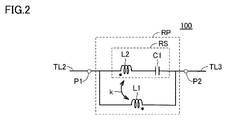
- FIG. 2 is an equivalent circuit diagram of the filter device 100.
- Terminal P1 is a terminal for connecting filter device 100 to transmission line TL2.
- Terminal P2 is a terminal for connecting filter device 100 to transmission line TL3 on the antenna 155 side.
- the terminal P1 When the feed circuit RF1 supplies a high frequency signal to the antenna 155 through the filter device 100, the terminal P1 becomes an input terminal and the terminal P2 becomes an output terminal.
- the terminal P1 When the high-frequency signal received by the antenna 155 is transmitted to the circuit on the power supply circuit RF1 side through the filter device 100, the terminal P1 becomes an output terminal and the terminal P2 becomes an input terminal.
- Filter device 100 does not have a ground electrode and is constructed as an integrated component.
- the filter device 100 includes an inductor L1, an inductor L2, and a capacitor C1.
- the LC series resonator RS is an LC series resonator formed by connecting an inductor L2 and a capacitor C1 in series.
- An LC series resonator RS is arranged between terminals P1 and P2.
- the inductor L1 is connected in parallel with the LC series resonator RS. That is, inductor L1 is also arranged between terminal P1 and terminal P2.
- the LC parallel resonator RP is an LC parallel resonator formed by connecting the inductor L1 and the LC series resonator RS in parallel.
- the inductor L1 and the inductor L2 are magnetically coupled in a direction that strengthens the magnetic fluxes. Thereby, a mutual inductance M is generated between the inductor L1 and the inductor L2.
- Magnetic coupling between inductor L1 and inductor L2 is additive coupling. That is, when current flows from the terminal P1 to the terminal P2 in FIG. 2, the direction of the magnetic field generated by the inductor L1 is opposite to the direction of the magnetic field generated by the inductor L2.
- the inductance of inductor L1 is smaller than the inductance of inductor L2.
- Filter device 100 uses LC parallel resonator RP and LC series resonator RS shown in FIG.
- the filter device 100 may also include other components such as impedance matching circuits and switches.
- a general LC parallel resonator means an LC parallel resonator in which only an inductor and a capacitor are connected in parallel, rather than an LC parallel resonator RP including an LC series resonator RS as shown in FIG. .
- FIG. 3 is a diagram for explaining the reactance characteristics of general LC parallel resonators 300M,N.
- lines LnM1, LnM2, LnN1, LnN2 representing reactances in the two LC parallel resonators 300M and 300N are shown.
- the horizontal axis indicates the frequency of the high frequency signal, and the vertical axis indicates the reactance value of the LC parallel resonator.
- the LC parallel resonator 300M and the LC parallel resonator 300N are examples of general LC parallel resonators in which an inductor and a capacitor are connected in parallel. have different inductance values of inductors and different capacitance values of capacitors.
- the inductance of the inductor of the LC parallel resonator 300N is 1 nH, and the capacitance of the capacitor is 3 pF.
- the inductance of the inductor of the LC parallel resonator 300M is 3 nH and the capacitance of the capacitor is 1 pF.
- Lines LnN1 and LnN2 represent the reactance of the LC parallel resonator 300N.
- Lines LnM1 and LnM2 represent the reactance of the LC parallel resonator 300M.
- the LC parallel resonator 300N resonates in a frequency band between the frequency at which the absolute value of the line LnN1 converges to infinity and the frequency at which the absolute value of the line LnN2 converges to infinity. As a result, the frequency band becomes the attenuation band d2 in the LC parallel resonator 300N.
- the LC parallel resonator 300M resonates in a frequency band between the frequency at which the absolute value of the line LnM1 converges to infinity and the frequency at which the absolute value of the line LnM2 converges to infinity. As a result, the frequency band becomes the attenuation band d1 in the LC parallel resonator 300M.
- LC parallel resonators 300M and 300N are configured such that attenuation band d1 and attenuation band d2 are included in the frequency band of f2 band.
- the attenuation band d2 of the LC parallel resonator 300N whose inductor inductance is smaller than that of the LC parallel resonator 300M is narrower than the attenuation band d1 of the LC parallel resonator 300M. That is, in a general LC parallel resonator in which an inductor and a capacitor are connected in parallel, reducing the inductance of the parallel-connected inductor narrows the attenuation band and improves steepness.
- the inductor L1 in the LC parallel resonator RP shown in FIG. 2 corresponds to the inductor in the general LC parallel resonators 300M, N described in FIG. That is, in the filter device 100 having the equivalent circuit configuration shown in FIG. 2, the attenuation band of the filter device 100 can be narrowed by reducing the inductor L1 corresponding to the inductor of a general LC parallel resonator. can.
- FIG. 4 is a diagram for explaining the inductive reactance required for resonance of the LC parallel resonator RP.
- the horizontal axis indicates the frequency of the high frequency signal, and the vertical axis indicates the reactance value.
- Filter device 100 is an example of a filter device having the equivalent circuit shown in FIG. As shown in FIG. 2, in the filter device 100, an additive magnetic coupling is performed between the inductor L1 and the inductor L2.
- the filter device 100Q of the comparative example is a filter device in which magnetic coupling is not made between the inductors L1 and L2. Filter device 100Q has the same configuration as filter device 100, except that magnetic coupling is not performed between inductor L1 and inductor L2.
- a line LnP indicates the capacitive reactance of the LC series resonator RS in the filter device 100 .
- Line LnQ represents the capacitive reactance of the LC series resonator RS in filter device 100Q.
- the capacitive reactance rc3 of the LC series resonator RS in the filter device 100 is higher than the capacitive reactance rc4 of the LC series resonator RS in the filter device 100Q. This is because the mutual inductance M corresponding to the coupling coefficient k is generated by the magnetic coupling between the inductors L1 and L2.
- the capacitive reactance values of the LC series resonators RS in the filter devices 100 and 100Q are both 0 in the f1 band. That is, a high-frequency signal having a frequency belonging to the f1 band passes through LC series resonators RS in filter device 100 and filter device 100Q. As a result, filter device 100 and filter device 100Q can pass high-frequency signals in the f1 band, which is the passband.
- a dashed line LnQp indicates the inductive reactance of the inductor L1 in the filter device 100Q.
- the value of the inductive reactance of the inductor L1 in order to resonate the LC parallel resonator RP in the f2 band, the value of the inductive reactance of the inductor L1 must be the inductive reactance rc1 shown in FIG. That is, the absolute value of the inductive reactance rc1 is the same as the absolute value of the capacitive reactance rc4.
- a dashed line LnPp indicates the inductive reactance of inductor L1 of filter device 100 .
- the value of the inductive reactance of the inductor L1 must be the inductive reactance rc2 shown in FIG. That is, the absolute value of the inductive reactance rc2 is the same as the absolute value of the capacitive reactance rc3.
- the inductive reactance rc2 required to resonate the LC parallel resonator RP in the filter device 100 is smaller than the inductive reactance rc1. This is because the mutual inductance M results in the capacitive reactance rc3 being higher than the capacitive reactance rc4.
- the inductive reactance rc2 itself also reduces the value of the inductor L1 because the mutual inductance M is added to the inductance of the inductor L1.
- inductor L1 and inductor L2 are magnetically coupled with added polarity, so that the inductance of inductor L1 can be reduced compared to filter device 100Q.
- depolarizing magnetic coupling may be performed instead of additive coupling if the inductance of inductor L1 is smaller than that of inductor L2.
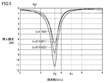
- FIG. 5 is a diagram showing an example of the insertion loss of filter device 100 in Embodiment 1 and the insertion loss of filter devices 100Z1 and 100Z2 of comparative examples.
- FIG. 5 shows lines Ln1 to Ln3 indicating insertion losses of filter device 100 according to the first embodiment and filter devices 100Z1 and 100Z2 of the comparative example.
- the horizontal axis indicates the frequency of the high frequency signal
- the vertical axis indicates the insertion loss of the high frequency signal.
- the insertion loss is the ratio of the power that is output to the power that is input to the filter device 100 . If the insertion loss is large, high-frequency signals are less likely to pass through the filter device, and if the insertion loss is small, high-frequency signals are more likely to pass through the filter device.
- a line Ln1 indicates the waveform of the insertion loss of the filter device 100 according to the first embodiment.
- a line Ln2 indicates the waveform of the insertion loss of the filter device 100Z1 in the comparative example.
- a line Ln3 indicates the waveform of the insertion loss of the filter device 100Z2 in the comparative example.
- Each of filter device 100, filter device 100Z1, and filter device 100Z2 is an example of a filter device having a configuration similar to that of LC parallel resonator RP shown in FIG. 2, but differs in the following points.
- inductor L1 has an inductance of 0.775 nH
- inductor L2 has an inductance of 0.997 nH
- capacitor C1 has a capacitance of 0.885 pF. Additive magnetic coupling.
- inductor L1 has an inductance of 1.195 nH
- inductor L2 has an inductance of 1.417 nH
- capacitor C1 has a capacitance of 0.885 pF
- inductor L1 and inductor L2 are depolarized. magnetic coupling.
- the inductance of inductor L1 is 0.997 nH
- the inductance of inductor L2 is 0.775 nH
- the capacitance of capacitor C1 is 0.885 pF
- inductor L1 and inductor L2 have additive polarity. magnetic coupling.
- the filter device 100Z1 of the comparative example differs from the filter device 100 of the first embodiment in that the magnetic coupling between the inductors L1 and L2 is depolarizing coupling.
- Filter device 100Z2 of the comparative example differs from filter device 100 of the first embodiment in that the inductance of inductor L1 is greater than the inductance of inductor L2.
- the inductances of the inductors L1 and L2 and the capacitance of the capacitor C1 are not limited to the above values. Also, the inductance values of the inductors L1 and L2 and the capacitance value of the capacitor C1 of each filter device include stray capacitance and stray inductance.
- the frequency at which each line Ln1 to Ln3 attenuates is the frequency F2. That is, the frequency F2 is the resonance frequency of the LC parallel resonator RP. Moreover, the frequency F2 is a frequency belonging to the f2 band, which is an attenuation band. Therefore, as shown in FIG. 5, in any one of the filter devices 100, 100Z1, and 100Z2, the insertion loss is the largest at the frequency F2 in the f2 band. On the other hand, the frequency F1 belongs to the f1 band, which is the passband. The insertion loss of frequencies belonging to the f1 band in filter devices 100, 100Z1, and 100Z2 will be described below with reference to FIG.
- the frequency F2 is treated as an arbitrary frequency belonging to the f2 band
- the frequency F1 is treated as an arbitrary frequency belonging to the f1 band. That is, the frequency F2 may be a frequency belonging to the f2 band, and the frequency F1 may be a frequency belonging to the f1 band.
- FIG. 6 is an enlarged view along the vertical axis of region Rg1 shown in FIG.
- FIG. 6 shows a waveform in which the vertical axis (insertion loss) direction of the region Rg1 shown in FIG. 5 is enlarged.
- the ratios in the horizontal axis (frequency) direction in FIG. 6 are the same as those in FIG. 5, and only the ratios in the vertical axis (insertion loss) direction are enlarged.
- the insertion loss when a high-frequency signal of frequency F1 passes is 0.418 dB for line LN1, 0.468 dB for line LN2, and 0.773 dB for line LN3.
- the insertion loss of the filter device 100 according to the first embodiment is the smallest among the filter device 100 according to the first embodiment and the filter devices 100Z1 and 100Z2 according to the comparative examples. That is, filter device 100 according to Embodiment 1 uses the f2 band as an attenuation band, as in filter devices 100Z1 and Z2, while the high-frequency signal of frequency F1 belonging to the f1 band, which is the passband, is higher than that of filter devices 100Z1 and Z2. is the easiest to pass.
- the inductance of the inductor L1 is smaller than the inductance of the inductor L2.
- the insertion loss in the f1 band can be made smaller than in the comparative example. That is, in the filter device 100 of Embodiment 1, it is possible to suppress loss that occurs when passing a high frequency signal in the f1 band.
- the inductance of the inductor L1 can be made smaller, so that the steepness of the attenuation band can be further improved. becomes possible.
- FIG. 7 is a diagram showing an example of the insertion loss of the filter device 100 according to Embodiment 1 and the insertion loss of the filter device Z3 of the comparative example.
- FIG. 7 shows lines Ln4 and Ln5 indicating the insertion loss of filter device 100 according to the first embodiment and the filter device of the comparative example.
- the horizontal axis indicates the frequency of the high frequency signal
- the vertical axis indicates the insertion loss of the high frequency signal.
- filter device 100 and LC parallel resonator RP of filter device 100Z3 are adjusted so that resonance frequency F2 is 4.35 GHz.
- a line Ln4 indicates the waveform of the insertion loss of the filter device 100 according to the first embodiment.
- a line Ln5 indicates the waveform of the insertion loss of the filter device 100Z3 in the comparative example.
- Filter device 100 and filter device 100Z3 have the same configuration, but filter device 100Z3 is connected to 50 ⁇ transmission line TL2 and 50 ⁇ transmission line TL3.
- the filter device 100 is connected between the 5 ⁇ transmission line TL2 and the 5 ⁇ transmission line TL3.
- the ratio between the characteristic impedance of the transmission line and the characteristic impedance of filter device 100 is increased by being connected to transmission lines TL1 and TL2 whose characteristic impedance is lower than 50 ⁇ .
- the characteristic impedances of the transmission line TL2 and the transmission line TL3 may be other values as long as they are less than 50 ⁇ .
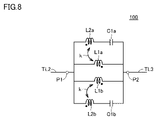
- FIG. 8 is a diagram showing a circuit configuration in which LC parallel resonators RP are connected in parallel.
- FIG. 9 is an exploded view of filter device 100 formed as an integral element.
- FIG. 8 shows a filter device 100 having a circuit configuration that realizes the equivalent circuit shown in FIG. 2 by connecting the LC parallel resonators RP shown in FIG. 2 in parallel.
- Inductor L1a and inductor L1b in FIG. 8 function as inductor L1 in FIG.
- inductor L2a and inductor L2b in FIG. 8 function as inductor L2 in FIG.
- Capacitor C1a and capacitor C1b in FIG. 8 function as capacitor C1 in FIG.
- the inductor L2a and the inductor L1a are magnetically coupled with additive polarity.
- the inductor L2b and the inductor L1b are magnetically coupled with additive polarity.
- the inductor L2 shown in FIG. 2 includes an inductor L2a (fifth inductor) and an inductor L2b (sixth inductor) arranged in a laminate.
- capacitor C1 shown in FIG. 2 includes capacitor C1a and capacitor C1b arranged in a stack.
- the filter device 100 is constructed by stacking ten dielectric layers Ly1 to Ly10. That is, the filter device 100 includes a laminated body in which dielectric layers Ly1 to Ly10 are laminated.
- FIG. 9 shows a state in which each of the dielectric layers Ly1 to Ly10 is viewed from above.
- the shaded area means an electrode for transmitting a high frequency signal
- the circular shape means the end of a via connecting each dielectric layer.
- Terminals in1, in2, in3, and in4 are provided on the dielectric layers Ly3, Ly5, Ly6, and Ly8, respectively. Each of terminals in1, in2, in3 and in4 is connected to terminal P1 in FIG. Terminals out1, out2, out3, and out4 are provided on the dielectric layers Ly2, Ly4, Ly7, and Ly9, respectively. Each of terminals out1, out2, out3 and out4 is connected to terminal P2 in FIG.
- winding-shaped electrodes included in the dielectric layer Ly1, the dielectric layer Ly2, and the dielectric layer Ly3 form an inductor L2a.
- Plate-shaped electrodes included in the dielectric layer Ly1, the dielectric layer Ly2, the dielectric layer Ly3, and the dielectric layer Ly4 form a capacitor C1a.
- the winding-shaped electrodes included in the dielectric layers Ly4 and Ly5 form an inductor L1a.
- a wire-shaped electrode included in the dielectric layers Ly6 and Ly7 forms an inductor L1b.
- the winding-shaped electrodes included in the dielectric layers Ly8, Ly9, and Ly10 form an inductor L2b.
- Plate-shaped electrodes included in the dielectric layer Ly7, the dielectric layer Ly8, the dielectric layer Ly9, and the dielectric layer Ly10 form a capacitor C1b.
- the steepness of the attenuation band is improved by reducing the inductance of the inductor L1.
- the inductor L1 and the inductor L2 are magnetically coupled with additive polarity. This produces a mutual inductance M, and the inductance of inductor L1 becomes smaller.
- inductor L1a and inductor L1b are arranged in parallel. Specifically, the inductor L1a is formed by the electrodes of the dielectric layers Ly4 and Ly5, and the inductor L1b is formed by the electrodes of the dielectric layers Ly6 and Ly7 adjacent to the dielectric layers Ly4 and Ly5.
- the mutual inductance M due to the additive magnetic coupling between the inductors L1a and L2a can be increased without increasing the combined inductance of the inductors L1a and L1b. can be done.
- Magnetic coupling between inductor L1a and inductor L1b can increase the inductance of inductor L1a and inductor L1b.
- the filter device 100 of FIG. 9 is configured such that the winding direction of the inductor L1a and the winding direction of the inductor L1b are different. Specifically, as indicated by an arrow Ar1, the winding electrode of the dielectric layer Ly5 turns counterclockwise from the terminal in2. After that, the winding electrodes of the dielectric layer Ly5 are connected to the winding electrodes of the dielectric layer Ly4 through vias. The winding electrode of dielectric layer Ly4 turns counterclockwise further from the end of the via, as indicated by arrow Ar2. That is, as indicated by arrows Ar1 and Ar2, the winding direction of the inductor L1a when the laminate is planarized is counterclockwise (counterclockwise).
- the winding electrode of the dielectric layer Ly6 turns clockwise from the terminal in3.
- the winding electrodes of the dielectric layer Ly6 are connected to the winding electrodes of the dielectric layer Ly7 through vias.
- the winding electrode of dielectric layer Ly7 turns clockwise further from the end of the via, as indicated by arrow Ar4. That is, as indicated by arrows Ar3 and Ar4, the winding direction of the inductor L1b when the laminate is planarized is clockwise (rightward).
- the winding directions of the inductors L1a and L1b are opposite to each other, which reduces the overlap between the inductors L1a and L1b in plan view.
- the magnetic coupling between the inductor L1a and the inductor L1b is reduced, and the inductance of the inductor L1a and the inductor L1b is prevented from increasing. can be placed in adjacent dielectric layers.
- the area where the winding forming the inductor L2a in the multilayer body Ly3 overlaps the winding forming the inductor L1a in the multilayer body Ly4 is the same as that of the winding forming the inductor L1a in the multilayer body Ly5. is greater than the area overlapping the winding forming inductor L2a in .
- the coupling coefficient of the magnetic coupling between inductor L2a and inductor L1a can be increased, and the inductance of inductor L1a can be further reduced.
- the coupling coefficient of the magnetic coupling between inductor L2b and inductor L1b can be increased, and the inductance of inductor L1b can be made smaller.
- the inductors L1a, L1b, L2a, and L2b are arranged so as not to overlap the capacitors C1a and C1b when the laminates Ly1 to Ly10 are viewed from above. .
- the magnetic flux generated by the magnetic coupling between the inductors L1a and L2a and the magnetic flux generated by the magnetic coupling between the inductors L1b and L2b can be increased without interrupting the magnetic flux generated by the magnetic coupling between the inductors L1a and L2b. You can prevent it from increasing.
- the filter device 100 of the first embodiment may have a configuration including any one of the dielectric layers Ly1 to Ly5 or Ly6 to Ly10 of the laminate in FIG.
- Embodiment 2 In Embodiment 1 above, the antenna device 150 having the antenna 155 has been described. In Embodiment 2, antenna module 200 including antenna device 160 in addition to antenna device 150 in Embodiment 1 will be described. In antenna module 200 of the second embodiment, description of the configuration overlapping with antenna device 150 of the first embodiment will not be repeated.
- FIG. 10 is a diagram showing the configuration of antenna module 200 according to the second embodiment.
- Antenna module 200 includes antenna device 150 and antenna device 160 .
- Antenna device 160 includes a feeding circuit RF2 and an antenna 165 .
- the antenna module 200 is installed in, for example, a mobile terminal such as a mobile phone, a smart phone, or a tablet, or a communication device such as a personal computer having a communication function.
- the feeding circuit RF1 supplies the antenna 155 with high-frequency signals in the frequency bands of the f1 band and the f3 band.
- Antenna 155 can radiate into the air, as radio waves, high-frequency signals in the f1 band and f3 band supplied from feeder circuit RF1.
- the frequency band of the f1 band is, for example, the Wi-Fi 5 GHz band (5.15-5.7 GHz).
- the frequency band of the f3 band is, for example, the Wi-Fi 2 GHz band (2.4-2.48 GHz).
- the filter device 100 is configured to attenuate high frequency signals in the f2 frequency band.
- the frequency band of the f2 band is, for example, a band such as n77 (3.3-4.2 GHz) of 5G-NR.
- the f2 band is not limited to n77 (3.3-4.2 GHz), but includes n78 (3.3-3.8 GHz) and n79 (4.4-4.9 GHz) in addition to n77. good too.
- the f1 and f3 bands are passbands, and the f2 band is an attenuation band.
- the f2 band is a frequency band between the f1 band and the f3 band.
- the f2 band frequency band is lower than the f1 band frequency band.
- the frequency band of the f3 band is lower than the frequency band of the f2 band.
- the f1 band is the highest frequency band and the f3 band is the lowest frequency band.
- the relationship among the f1 band, f2 band, and f3 band is such that the f1 band, f2 band, and f3 band become lower in the order of f1 band, f2 band, and f3 band, each of the f1 band, f2 band, and f3 band is a different frequency band.
- the resonance frequency F2 of the LC parallel resonator RP of the filter device 100 according to the second embodiment is adjusted to be 3.8 GHz, which is near the median value of the f2 band according to the second embodiment.
- the feeding circuit RF2 supplies the antenna 165 with a high-frequency signal in the frequency band of the f2 band.
- the antenna 165 can radiate into the air the f2-band high-frequency signal supplied from the feeder circuit RF2 as radio waves.
- the filter device 100 is provided to remove the f2 band high-frequency signal, which may become noise in the antenna device 150, by increasing the insertion loss due to parallel resonance.
- the antenna 155 and the antenna 165 are mounted on the same substrate 170. Although the antennas 155 and 165 are provided on the same substrate 170 in FIG. 10, they may be provided on different substrates as long as they are provided in the same antenna module 200. FIG. Further, in the second embodiment, the power feeding circuit RF1 may not supply the high frequency signal in the f3 band, but may supply only the high frequency signal in the f1 band.
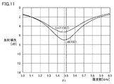
- FIG. 11 is a diagram showing an example of the return loss of the antenna device 150 according to Embodiment 2 and the return loss of the antenna device 150Z of the comparative example.
- the horizontal axis indicates the frequency of the high frequency signal, and the vertical axis indicates the return loss of the high frequency signal.
- the reflection loss indicates the ratio of the reflected power to the power supplied from the feeding circuit RF1 of the antenna device 150. FIG. That is, when power is radiated from the antenna, reflection loss also increases.
- a line Ln6 shows the waveform of the return loss of the antenna device 150 in the second embodiment.
- a line Ln7 indicates the waveform of the return loss of the antenna device 150Z in the comparative example.
- the antenna device 150Z has a configuration obtained by removing the filter device 100 from the antenna device 150 shown in FIG. That is, the antenna device 150 of the second embodiment and the antenna device 150Z of the comparative example differ in whether or not the filter device 100 is provided.
- the return loss of the antenna device 150 according to the second embodiment including the filter device 100 is as compared to that of the antenna device 150Z of the comparative example. growing. That is, by providing the filter device 100, the antenna characteristics of the antenna device 150 are improved as compared with the antenna device 150Z of the comparative example. Lines Ln7 and Ln6 both attenuate at frequency F1. In other words, between the antenna device 150 and the antenna device 150Z, the series resonance of the filter device 100 does not cause a shift in impedance frequency, and matching can be maintained. In other words, impedance matching does not deteriorate depending on whether or not the filter device 100 is provided. Therefore, in the antenna module 200 of Embodiment 2, the filter device 100 can be mounted on the antenna device 150 without re-matching the deterioration of the impedance.
- FIG. 12 is a diagram showing isolation characteristics between the antenna device 150 and the antenna device 160.
- FIG. The horizontal axis indicates the frequency of the high frequency signal, and the vertical axis indicates the isolation of the high frequency signal. That is, the isolation is the ratio of the power received by the feeder circuit RF2 of the antenna device 160 via the antenna to the power input from the feeder circuit RF1 of the antenna device 150 .
- a line Ln8 indicates the isolation between the antenna device 150 and the antenna device 160 of the antenna module 200 in the second embodiment.
- a line Ln9 indicates the isolation between the antenna device 150 and the antenna device 160 of the antenna module 200Z in the comparative example.
- the antenna module 200Z has a configuration obtained by removing the filter device 100 from the antenna module 200 of FIG. That is, the antenna module 200 of the second embodiment and the antenna module 200Z of the comparative example differ in whether or not the filter device 100 is provided.
- the antenna module 200 of Embodiment 2 has an isolation of 15 dB or more greater than that of the antenna module 200Z of the comparative example. That is, in the second embodiment, filter device 100 attenuates frequencies in the f2 band, thereby improving the isolation of antenna devices 150 and 160 compared to the comparative example.
- FIG. 13 is a diagram showing the radiation efficiency of the antenna device 160.
- FIG. The horizontal axis indicates the frequency of the high frequency signal, and the vertical axis indicates the radiation efficiency of the antenna device 160 .
- a line Ln10 indicates the radiation efficiency of the antenna device 160 of the antenna module 200 in the second embodiment.
- a line Ln11 indicates the radiation efficiency of the antenna device 160 of the antenna module 200Z in the comparative example.
- the radiation efficiency means the ratio of the power radiated from the antenna to the power supplied from the feeding circuit. That is, in FIG. 13, the power radiated from the antenna increases toward the top of the graph for the same supplied power.
- the radiation efficiency of the antenna module 200 of Embodiment 2 is improved by about 4.5 dB compared to the antenna module 200Z of the comparative example. That is, in the second embodiment, the antenna device 150 is provided with the filter device 100, so that the radiation efficiency of the antenna device 160 can be improved more than the comparative example.
- the filter device 100Z2 of the comparative example differs from the filter device 100 of the second embodiment in that the inductance of the inductor L1 is larger than the inductance of the inductor L2.
- FIG. 14 is a diagram showing synthetic reactance characteristics of the LC parallel resonator RP according to the second embodiment.
- the horizontal axis indicates the frequency of the high-frequency signal
- the vertical axis indicates the synthetic reactance value of the LC parallel resonator RP.
- a line Ln15 indicates the value of the combined reactance of the LC parallel resonator RP of the filter device 100 according to the second embodiment.
- a line Ln14 indicates the value of the combined reactance of the LC parallel resonator RP in the filter device 100Z2 when the filter device 100Z2 of the comparative example is applied.
- the value of the combined reactance at frequency F1 in the f1 band and frequency F3 in the f3 band, which are the passbands, is higher than that of the comparative example. become smaller.
- high-frequency signals of frequencies F1 and F3 included in the passband pass through filter device 100 more easily than through filter device 100Z2.
- the frequency F3 is treated as any frequency belonging to the f3 band. That is, the frequency F3 may be any frequency belonging to the f3 band.
- FIG. 15 is a diagram showing the insertion loss of the filter device 100 according to the second embodiment.
- Line Ln13 indicates the insertion loss of filter device 100 of antenna module 200 in the second embodiment.
- a line Ln14 indicates the insertion loss of the filter device 100Z2 when the filter device 100Z2 in the comparative example is applied to the second embodiment.
- the combined reactance is small at the frequency F1 of the f1 band and the frequency F3 of the f3 band, which are the passbands, as shown in FIG.
- the insertion loss of the filter device 100 is smaller than that of the filter device 100Z2 of the comparative example.
- filter device 100 since the inductance of inductor L1 is smaller than the inductance of inductor L2, filter device 100 according to the second embodiment can more easily pass high-frequency signals having frequencies F1 and F3 in passbands closer to the attenuation band than in the comparative example. Become.
- the f2 band is used as the attenuation band by setting the resonance frequency of the LC parallel resonator RP to the frequency F2 included in the f2 band.
- a high-frequency signal with a frequency F3 lower than the f2 band passes through the path in which the inductor L1 is arranged rather than the path of the LC series resonator RS. That is, when a high-frequency signal in the f3 band passes through, the path in which the inductor L1 is arranged becomes dominant.
- the inductance of inductor L1 is made smaller than the inductance of inductor L2 in order to narrow the attenuation band. This reduces the impedance when the frequency F3 passes through the inductor L1.
- the frequency F2 is efficiently radiated from the feeder circuit RF2, and the attenuation band is narrowed compared to the filter device 100Z2, thereby reducing the frequencies F1 and F3. Efficient radiation from the feeding circuit RF1 becomes possible.
- FIG. 16 is a diagram showing the insertion loss of the antenna 155 in Embodiment 2.
- FIG. A line Ln17 indicates the insertion loss of the antenna 155 of the antenna module 200 in the second embodiment.
- a line Ln18 indicates the insertion loss of the antenna 155Z in the comparative example.
- a line Ln19 indicates the insertion loss of the antenna 155Z1 in the comparative example.
- the antenna 155Z is an antenna obtained by removing the filter device 100 from the antenna device 150 shown in FIG.
- Antenna 155Z1 has a configuration including filter device 100Z2 instead of filter device 100 in antenna 155 shown in FIG.
- the frequency at which the line Ln17 has a large insertion loss approaches the frequency at which the line Ln18 has a large insertion loss rather than the frequency at which the line Ln19 has a large insertion loss. That is, impedance matching does not deteriorate when filter device 100 according to the second embodiment is mounted, compared to when filter device 100Z2 is mounted. Therefore, the filter device 100 of the second embodiment imposes less load on impedance matching when applied to the antenna module 200 than the filter device 100Z2 of the comparative example.
- the configuration designed so that the resonance frequency F2 of the LC parallel resonator RP of the filter device 100 is 3.8 GHz within the f2 band has been described.
- a filter device 100B designed such that the resonance frequency F2 of the LC parallel resonator RP is near the lower limit of the frequency band of the f2 band will be described.
- the frequency band of the f2 band is the 5G-NR n78 (3.3-3.8 GHz) band. That is, the resonance frequency F2 of the LC parallel resonator RP of the filter device 100B is 3.3 GHz.
- the filter device 100A is used as a comparative example for the filter device 100B.
- the resonance frequency F2 of the LC parallel resonator RP of the filter device 100A of the comparative example is adjusted to 3.5 GHz within the frequency band of the f2 band.
- filter device 100B according to the modification of the second embodiment descriptions of configurations that overlap those of the first and second embodiments will not be repeated.
- FIG. 17 is a diagram showing an example of the insertion loss of the filter device 100B in the modified example of the second embodiment and the insertion loss of the filter device 100A of the comparative example.
- 17 to 19 show frequency f2s indicating a frequency of 3.3 GHz near the lower limit of the f2 band, frequency f2c indicating a frequency of 3.5 GHz near the center of the f2 band, and frequency 3 near the upper limit of the f2 band.
- a frequency f2e representing 0.8 GHz is shown.
- antenna modules to which filter device 100A and filter device 100B are applied instead of filter device 100 in the second embodiment are referred to as antenna modules 250A and 250B, respectively.
- a line Ln20 shown in FIG. 17 indicates the insertion loss of the antenna device 150 of the antenna module 250B in the modified example of the second embodiment.
- a line Ln21 indicates the insertion loss of the antenna device 150 of the antenna module 250A of the comparative example in the modified example of the second embodiment.
- the resonance frequency F2 in the filter device 100B is designed to be the frequency f2s (3.3 GHz) near the lower limit of the n78 band. Note that the resonance frequency in filter device 100B may be, for example, 3.2 GHz or 3.4 GHz instead of 3.3 GHz.
- the resonance frequency F2 in the filter device 100A is designed to be the frequency f2c (3.5 GHz).
- FIG. 18 is a diagram showing an example of the radiation efficiency of the antenna device 150 in the modified example of Embodiment 2 and the radiation efficiency of the antenna device 150 in the comparative example.
- a line Ln22 shown in FIG. 18 indicates the radiation efficiency of the antenna device 150 of the antenna module 250B in the modified example of the second embodiment.
- a line Ln23 indicates the radiation efficiency of the antenna device 150 of the antenna module 250A of the comparative example in the modified example of the second embodiment.
- a line Ln24 indicates the radiation efficiency of the antenna device 150 of the antenna module 200Z of the comparative example in the modified example of the second embodiment.
- the antenna module 200Z has a configuration obtained by removing the filter device 100 from the antenna module 200 of FIG.
- the radiation efficiency of the antenna module 250A of the comparative example is lower than the radiation efficiency of the antenna module 200Z of the comparative example in the frequency band from the frequency f2s to the frequency f2c, especially around the frequency F2s.
- the radiation efficiency of antenna module 200B which is a modification of Embodiment 2
- the radiation efficiency of antenna module 200B is higher than that of antenna module 200Z of the comparative example in the frequency band from frequency F2s to frequency f2c. That is, the radiation efficiency of the antenna module 200B, which is a modification of the second embodiment, is higher than that of the antenna module 200Z of the comparative example in the entire f2 band (band from frequency f2s to frequency f2e).
- FIG. 19 is a diagram showing isolation characteristics between the antenna device 150 and the antenna device 160 in the modified example of the second embodiment.
- Line Ln25 indicates the isolation between antenna device 150 and antenna device 160 of antenna module 250B in the modification of the second embodiment.
- a line Ln26 indicates the isolation between the antenna device 150 and the antenna device 160 of the antenna module 200Z in the comparative example.
- the antenna module 250B has greater isolation than the antenna module 200Z of the comparative example. That is, in the modification of the second embodiment, filter device 100B attenuates frequencies in the f2 band, thereby improving the isolation of antenna devices 150 and 160 compared to the comparative example.
- the filter device 100B is adjusted so that the resonance frequency F2 is near the lower limit of the f2 band, which is the attenuation band.
- the resonance frequency F2 of the filter device 100B may be a frequency near the lower limit of the attenuation band, and may be a frequency lower than the lower limit of the attenuation band.
- FIG. 20 is an external view of the antenna module 201 in which the antenna 155 is an inverted F-type antenna. As shown in FIG. 20, antenna 155 is formed as an inverted F antenna. Antenna 165 is formed as a monopole antenna. As shown in FIG. 20, antenna 155 is connected to feeder circuit RF1 through filter device 100 .
- the antenna 155 which is an inverted F-type antenna, is branched from the path connecting to the feeding circuit RF1 and connected to the ground electrode GND.
- a branching point will be referred to as a branching point between a path connecting to the feeder circuit RF1 and a path connecting to the ground electrode GND.
- FIG. 21 is a diagram showing the radiation efficiency of the antenna 165 when the antenna 155 is an inverted F antenna.
- a line LnF1 indicates the radiation efficiency of the antenna 165 of the antenna module 201Z of the comparative example.
- a line LnF2 indicates the radiation efficiency of the antenna 165 of the antenna module 201 of the second embodiment.
- a line LnF3 indicates the radiation efficiency of the antenna 165 of the antenna module 201A of the first modification.
- a line LnF4 indicates the radiation efficiency of the antenna 165 of the antenna module 201B of the second modification.
- the antenna module 201Z of the comparative example does not include the filter device 100. That is, the antenna module 201Z has a configuration obtained by removing the filter device 100 from the antenna module 201 of FIG.
- the filter device 100 is not arranged on the path from the branch point to the feeder circuit RF1, but the filter device 100 is arranged on the path Rt from the branch point to the ground electrode GND. It has a configuration that
- Antenna module 201B of modification 2 has filter device 100 arranged on the path from the branch point to feed circuit RF1, and filter device 100 is arranged on path Rt from the branch point to ground electrode GND. It has a configuration that That is, the antenna device 150 of the antenna module 200B of Modification 2 includes two filter devices 100 .
- the radiation efficiency of the antenna 165 in the antenna module 201Z of the comparative example without the filter device 100 is the lowest. That is, in Embodiment 2 and Modifications 1 and 2 to which an inverted F-type antenna is applied, the radiation efficiency of antenna 165 is improved over the comparative example by providing filter device 100 .
- FIG. 22 is an external view of the antenna module 202 in which the antenna 155 is a loop antenna.
- antenna 155 is formed as a loop antenna.
- Antenna 165 is formed as a monopole antenna.
- the antenna 155 which is a loop antenna, is also connected to the ground electrode GND via a path Rt different from the path connecting to the feeding circuit RF1.
- FIG. 23 is a diagram showing the radiation efficiency of the antenna 165 when the antenna 155 is a loop antenna.
- a line LnL1 indicates the radiation efficiency of the antenna 165 of the antenna module 202Z of the comparative example.
- a line LnL2 indicates the radiation efficiency of the antenna 165 of the antenna module 202 of the second embodiment.
- a line LnL3 indicates the radiation efficiency of the antenna 165 of the antenna module 202A of the first modification.
- a line LnL4 indicates the radiation efficiency of the antenna 165 of the antenna module 202B of the second modification.
- An antenna module 202Z of the comparative example has a configuration obtained by removing the filter device 100 from the antenna module 202 of FIG.
- the filter device 100 is arranged not on the path between the antenna 155 and the feeder circuit RF1, but on the path Rt between the antenna 155 and the ground electrode GND. It has a configuration that
- antenna module 202B of Modification 2 filter device 100 is arranged on the path from antenna 155 to feed circuit RF1, and filter device 100 is arranged on path Rt from antenna 155 to ground electrode GND. It has a configuration that
- the radiation efficiency of the antenna 165 in the antenna module 202Z of the comparative example without the filter device 100 is the lowest. That is, in Embodiment 2 and Modifications 1 and 2 to which the loop antenna is applied, the radiation efficiency of antenna 165 is improved by providing filter device 100 as compared to the comparative example.
- FIG. 24 is an external view of the antenna module 203 in which the antenna 155 is a patch antenna.
- antenna 155 is formed as a patch antenna.
- Antenna 165 is formed as a monopole antenna.
- antenna 155, which is a patch antenna is also connected to ground electrode GND via a path Rt different from the path connecting to feeder circuit RF1.
- FIG. 25 is a diagram showing the radiation efficiency of the antenna 165 when the antenna 155 is a patch antenna.
- a line LnP1 indicates the radiation efficiency of the antenna 165 of the antenna module 203Z of the comparative example.
- a line LnP2 indicates the radiation efficiency of the antenna 165 of the antenna module 203 of the second embodiment.
- a line LnP3 indicates the radiation efficiency of the antenna 165 of the antenna module 203A of the first modification.
- a line LnP4 indicates the radiation efficiency of the antenna 165 of the antenna module 203B of the second modification.
- An antenna module 203Z of the comparative example has a configuration obtained by removing the filter device 100 from the antenna module 203 of FIG.
- the filter device 100 is not arranged on the path between the antenna 155 and the feeder circuit RF1, but on the path Rt between the antenna 155 and the ground electrode GND.
- antenna module 203B of Modification 2 filter device 100 is arranged on the path from antenna 155 to feed circuit RF1, and filter device 100 is arranged on path Rt from antenna 155 to ground electrode GND. It has a configuration that
- the radiation efficiency of the antenna 165 in the antenna module 203Z of the comparative example without the filter device 100 is the lowest. That is, in Embodiment 2 and Modifications 1 and 2 to which the loop antenna is applied, the radiation efficiency of antenna 165 is improved by providing filter device 100 as compared to the comparative example.
- 100 filter device 150, 160 antenna device, 155, 165 antenna, 170 substrate, 200, 201, 202, 203, 250 antenna module, Ar1 to Ar4 arrows, C1a, C1b, C1 capacitors, F1 to F3, f2s, f2c, f2e Frequency, GND Ground electrode, L1, L1a, L1b, L2, L2b, L2a Inductor, Ly1 to Ly10 Dielectric layer, P1, P2, in1 to in4, out1 to out4 Terminals, RF1, RF2 Power supply circuit, RSLC series resonance device, RP LC parallel resonator, Rg1 region, SP connection point, TL1 to TL3 transmission line, d1, d2 attenuation band, M mutual inductance, rc1, rc2 inductive reactance, rc3, rc4 capacitive reactance, Rt path.
- Ar1 to Ar4 arrows C1a, C1b, C1 capacitors, F1
Landscapes
- Engineering & Computer Science (AREA)
- Power Engineering (AREA)
- Filters And Equalizers (AREA)
Abstract
In a filter device (100) according to another aspect of the present disclosure, a pass-band is in a first frequency band (f1 band), and an attenuation band lower than the first frequency band (f1 band) is in a second frequency band (f2 band). The filter device (100) comprises: a first terminal (P1); a second terminal (P2); a first inductor (L1) disposed between the first terminal (P1) and the second terminal (P2); and an LC series resonator (RS) connected in parallel to the first inductor (L1) and including a first capacitor (C1) and a second inductor (L2). The first inductor (L1) and the second inductor (L2) are magnetically coupled to each other. The inductance of the first inductor (L1) is less than the inductance of the second inductor (L2).
Description
本開示は、フィルタ装置、アンテナ装置、およびアンテナモジュールに関し、より特定的には、減衰帯域の急峻性を改善するための技術に関する。
The present disclosure relates to a filter device, an antenna device, and an antenna module, and more specifically to technology for improving the steepness of an attenuation band.
国際公開第2016/167171号(特許文献1)には、第1インダクタおよび第1キャパシタから構成される直列回路に対して、第2インダクタが並列に接続されているフィルタ装置が開示されている。第1インダクタと第2インダクタとは、磁束を互いに強め合う方向に磁界を介して結合している。
International Publication No. 2016/167171 (Patent Document 1) discloses a filter device in which a second inductor is connected in parallel to a series circuit composed of a first inductor and a first capacitor. The first inductor and the second inductor are coupled via a magnetic field in a direction in which magnetic fluxes are mutually strengthened.
特許文献1では、磁界結合により第1インダクタおよび第2インダクタの実効的なインダクタンスが大きくなるため、第1インダクタおよび第2インダクタの各々単体におけるインダクタンスは小さくなる。これにより、特許文献1のフィルタ装置では、並列共振器の抵抗成分を減少させ、Q値を向上させることができる。
In Patent Document 1, magnetic field coupling increases the effective inductance of the first inductor and the second inductor, so the inductance of each of the first inductor and the second inductor is reduced. Thereby, in the filter device of Patent Document 1, the resistance component of the parallel resonator can be reduced and the Q value can be improved.
近年、様々な周波数帯域の高周波が使用されるようになったことから、フィルタ装置においては、減衰帯域に近接した帯域を通過帯域とする場合がある。通過帯域が減衰帯域と近接する場合、特許文献1に示されているフィルタ装置において、減衰帯域の急峻性が十分でない場合がある。
In recent years, since high frequencies in various frequency bands have come to be used, in some filter devices, a band close to the attenuation band is used as the passband. If the passband is close to the attenuation band, the steepness of the attenuation band may not be sufficient in the filter device disclosed in Patent Document 1.
本開示は、このような課題を解決するためになされたものであり、その目的は高周波信号におけるフィルタ装置において、減衰帯域の急峻性を改善し、減衰帯域と近接する帯域の高周波信号を通過させる場合に発生する損失を抑制することである。
The present disclosure has been made to solve such problems, and its purpose is to improve the steepness of the attenuation band in a filter device for high-frequency signals, and pass high-frequency signals in a band close to the attenuation band. It is to suppress the loss that occurs in the case.
本開示の他の局面に従うフィルタ装置は、通過帯域が第1周波数帯であり、第1周波数帯よりも低い減衰帯域が第2周波数帯である。フィルタ装置は、第1端子と、第2端子と、第1インダクタと、LC直列共振器とを備える。第1インダクタは、第1端子と第2端子との間に配置される。LC直列共振器は、第1インダクタと並列に接続され、第1キャパシタおよび第2インダクタを含む。第1インダクタと第2インダクタとは、互いに磁気結合する。第1インダクタのインダクタンスは、第2インダクタのインダクタンスよりも小さい。
A filter device according to another aspect of the present disclosure has a first frequency band as a passband and a second frequency band as an attenuation band lower than the first frequency band. The filter device has a first terminal, a second terminal, a first inductor, and an LC series resonator. A first inductor is disposed between the first terminal and the second terminal. An LC series resonator is connected in parallel with the first inductor and includes a first capacitor and a second inductor. The first inductor and the second inductor are magnetically coupled to each other. The inductance of the first inductor is less than the inductance of the second inductor.
本開示によるフィルタ装置においては、LC並列共振器において、第1インダクタのインダクタンスは、第2インダクタのインダクタンスよりも小さくなるように構成される。このような構成とすることによって、第1インダクタのインダクタンスが第2インダクタのインダクタンスよりも大きくなる構成に比べて、減衰帯域の急峻性を改善することができ、減衰帯域と近接する帯域の高周波信号を通過させる場合に発生する損失を抑制することができる。
In the filter device according to the present disclosure, the inductance of the first inductor is configured to be smaller than the inductance of the second inductor in the LC parallel resonator. With such a configuration, compared to a configuration in which the inductance of the first inductor is larger than the inductance of the second inductor, the steepness of the attenuation band can be improved, and the high-frequency signal in the band adjacent to the attenuation band can be improved. It is possible to suppress the loss that occurs when passing through.
以下、本開示の実施の形態について、図面を参照しながら詳細に説明する。なお、図中同一または相当部分には同一符号を付してその説明は繰り返さない。
Hereinafter, embodiments of the present disclosure will be described in detail with reference to the drawings. The same or corresponding parts in the drawings are denoted by the same reference numerals, and the description thereof will not be repeated.
[実施の形態1]
<アンテナ装置の基本構成>
図1は、実施の形態1におけるアンテナ装置150の構成を示す図である。アンテナ装置150は、給電回路RF1と、フィルタ装置100と、アンテナ155とを含む。アンテナ装置150は、たとえば、携帯電話、スマートフォンあるいはタブレットなどの携帯端末や、通信機能を備えたパーソナルコンピュータなどの通信装置に搭載される。 [Embodiment 1]
<Basic Configuration of Antenna Device>
FIG. 1 is a diagram showing the configuration of anantenna device 150 according to Embodiment 1. As shown in FIG. Antenna device 150 includes a feeding circuit RF1, a filter device 100, and an antenna 155. FIG. The antenna device 150 is installed in, for example, a mobile terminal such as a mobile phone, a smart phone, or a tablet, or a communication device such as a personal computer having a communication function.
<アンテナ装置の基本構成>
図1は、実施の形態1におけるアンテナ装置150の構成を示す図である。アンテナ装置150は、給電回路RF1と、フィルタ装置100と、アンテナ155とを含む。アンテナ装置150は、たとえば、携帯電話、スマートフォンあるいはタブレットなどの携帯端末や、通信機能を備えたパーソナルコンピュータなどの通信装置に搭載される。 [Embodiment 1]
<Basic Configuration of Antenna Device>
FIG. 1 is a diagram showing the configuration of an
給電回路RF1は、f1帯の周波数帯域の高周波信号をアンテナ155に供給する。アンテナ155は、給電回路RF1から供給されたf1帯の高周波信号を電波として空気中に放射可能である。f1帯の周波数帯域は、たとえば、Wi-Fi(登録商標)の5GHz帯(5.15-5.7GHz)である。アンテナ155は、たとえば、モノポールアンテナである。
The feeding circuit RF1 supplies the antenna 155 with a high-frequency signal in the frequency band of the f1 band. The antenna 155 can radiate into the air, as radio waves, a high-frequency signal in the f1 band supplied from the feeder circuit RF1. The frequency band of the f1 band is, for example, the 5 GHz band (5.15-5.7 GHz) of Wi-Fi (registered trademark). Antenna 155 is, for example, a monopole antenna.
フィルタ装置100は、特定の周波数帯の高周波信号の通過を妨げ、減衰させるトラップフィルタである。フィルタ装置100は、バンドエリミネートフィルタとも称される。実施の形態1におけるフィルタ装置100は、f2帯の周波数帯域の高周波信号を減衰させるように構成されている。f2帯の周波数帯域は、5G-NR(New Radio)のn77(3.3-4.2GHz)、n78(3.3-3.8GHz)を含む帯域である。f1帯とf2帯とは近接する周波数帯域である。周波数帯域が近接するか否かは、たとえば、帯域幅とその帯域幅に対する中心周波数を用いて定められる。たとえば、f1帯の周波数端とf2帯の周波数端との帯域幅とその帯域幅に対する中心周波数の比が所定の範囲内にある場合、f1帯とf2帯とが近接していると判断する。なお、その他の手法によって、周波数帯域が近接しているか否かを定めてもよい。フィルタ装置100において、f1帯が通過帯域であってf2帯が減衰帯域である。
The filter device 100 is a trap filter that prevents passage of high-frequency signals in a specific frequency band and attenuates them. Filter device 100 is also referred to as a band-eliminating filter. The filter device 100 according to the first embodiment is configured to attenuate high frequency signals in the f2 frequency band. The frequency band of the f2 band includes 5G-NR (New Radio) n77 (3.3-4.2 GHz) and n78 (3.3-3.8 GHz). The f1 band and the f2 band are adjacent frequency bands. Whether or not frequency bands are adjacent is determined, for example, using a bandwidth and a center frequency for that bandwidth. For example, if the bandwidth between the frequency edge of the f1 band and the frequency edge of the f2 band and the ratio of the center frequency to the bandwidth are within a predetermined range, it is determined that the f1 band and the f2 band are close to each other. It should be noted that other methods may be used to determine whether or not the frequency bands are close to each other. In the filter device 100, the f1 band is the passband and the f2 band is the attenuation band.
アンテナ装置150は、伝送線路TL1,TL2,TL3を含む。伝送線路TL1と伝送線路TL2とは、接続点SPにおいて電気的に接続させる。伝送線路TL1(第1伝送線路)は、接続点SPから給電回路RF1または給電回路RF1側に配置されている他の構成までの伝送線路である。すなわち、伝送線路TL1の一端は、給電回路RF1または給電回路RF1側に配置されている他の構成と接続し、伝送線路TL1の他端は、接続点SPにおいて伝送線路TL2(第2伝送線路)と接続する。
The antenna device 150 includes transmission lines TL1, TL2, and TL3. The transmission line TL1 and the transmission line TL2 are electrically connected at the connection point SP. The transmission line TL1 (first transmission line) is a transmission line from the connection point SP to the feeder circuit RF1 or another component arranged on the feeder circuit RF1 side. That is, one end of the transmission line TL1 is connected to the feeder circuit RF1 or another component arranged on the feeder circuit RF1 side, and the other end of the transmission line TL1 is connected to the transmission line TL2 (second transmission line) at the connection point SP. Connect with
伝送線路TL2は、接続点SPからフィルタ装置100までの伝送線路である。すなわち、伝送線路TL2の一端は接続点SPにおいて伝送線路TL1と接続し、伝送線路TL2の他端はフィルタ装置100と接続する。伝送線路TL3(第3伝送線路)は、フィルタ装置100からアンテナ155までの伝送線路である。すなわち、伝送線路TL3の一端はフィルタ装置100と接続され、伝送線路TL3の他端はアンテナ155と接続する。図1では、フィルタ装置100がアンテナ155に接続される例について説明したが、フィルタ装置100はパワーアンプ等に接続されてもよい。
The transmission line TL2 is a transmission line from the connection point SP to the filter device 100. That is, one end of the transmission line TL2 is connected to the transmission line TL1 at the connection point SP, and the other end of the transmission line TL2 is connected to the filter device 100. FIG. A transmission line TL 3 (third transmission line) is a transmission line from the filter device 100 to the antenna 155 . That is, one end of the transmission line TL3 is connected to the filter device 100 and the other end of the transmission line TL3 is connected to the antenna 155. FIG. Although FIG. 1 describes an example in which the filter device 100 is connected to the antenna 155, the filter device 100 may be connected to a power amplifier or the like.
<フィルタ装置100の等価回路図>
図2は、フィルタ装置100の等価回路図である。端子P1は、フィルタ装置100を伝送線路TL2と接続するための端子である。端子P2は、フィルタ装置100をアンテナ155側の伝送線路TL3と接続するための端子である。 <Equivalent Circuit Diagram ofFilter Device 100>
FIG. 2 is an equivalent circuit diagram of thefilter device 100. As shown in FIG. Terminal P1 is a terminal for connecting filter device 100 to transmission line TL2. Terminal P2 is a terminal for connecting filter device 100 to transmission line TL3 on the antenna 155 side.
図2は、フィルタ装置100の等価回路図である。端子P1は、フィルタ装置100を伝送線路TL2と接続するための端子である。端子P2は、フィルタ装置100をアンテナ155側の伝送線路TL3と接続するための端子である。 <Equivalent Circuit Diagram of
FIG. 2 is an equivalent circuit diagram of the
給電回路RF1がフィルタ装置100を介して高周波信号をアンテナ155に供給する場合、端子P1は入力端子となり、端子P2は出力端子となる。アンテナ155が受信した高周波信号がフィルタ装置100を介して給電回路RF1側の回路に伝達される場合、端子P1は出力端子となり、端子P2は入力端子となる。フィルタ装置100は、接地電極を有さず、一体化された部品として構成される。
When the feed circuit RF1 supplies a high frequency signal to the antenna 155 through the filter device 100, the terminal P1 becomes an input terminal and the terminal P2 becomes an output terminal. When the high-frequency signal received by the antenna 155 is transmitted to the circuit on the power supply circuit RF1 side through the filter device 100, the terminal P1 becomes an output terminal and the terminal P2 becomes an input terminal. Filter device 100 does not have a ground electrode and is constructed as an integrated component.
フィルタ装置100は、インダクタL1とインダクタL2とキャパシタC1とを備える。LC直列共振器RSは、インダクタL2とキャパシタC1とが直列接続されることによって形成されるLC直列共振器である。LC直列共振器RSは、端子P1と端子P2との間に配置される。
The filter device 100 includes an inductor L1, an inductor L2, and a capacitor C1. The LC series resonator RS is an LC series resonator formed by connecting an inductor L2 and a capacitor C1 in series. An LC series resonator RS is arranged between terminals P1 and P2.
インダクタL1は、LC直列共振器RSと並列に接続される。すなわち、インダクタL1も、端子P1と端子P2との間に配置される。LC並列共振器RPは、インダクタL1とLC直列共振器RSとが並列接続されることによって形成されるLC並列共振器である。
The inductor L1 is connected in parallel with the LC series resonator RS. That is, inductor L1 is also arranged between terminal P1 and terminal P2. The LC parallel resonator RP is an LC parallel resonator formed by connecting the inductor L1 and the LC series resonator RS in parallel.
インダクタL1とインダクタL2とは、磁束を互いに強め合う方向に磁気結合をする。これにより、インダクタL1とインダクタL2とに対して、相互インダクタンスMが発生する。インダクタL1とインダクタL2との磁気結合は、加極性結合である。すなわち、図2における端子P1から端子P2に向かって電流が流れる時に、インダクタL1で発生する磁界の方向とインダクタL2で発生する磁界の方向は逆である。実施の形態1のフィルタ装置100では、インダクタL1のインダクタンスは、インダクタL2のインダクタンスよりも小さい。フィルタ装置100は、図2に示すLC並列共振器RPおよびLC直列共振器RSを用いて、共振する周波数帯域の高周波信号を通過させずに減衰させる。なお、LC直列共振器RSにおいて、インダクタL2の配置とキャパシタC1の配置とは、逆であってもよい。また、フィルタ装置100は、インピーダンスを整合させる回路、スイッチなどの他の構成を含んでもよい。
The inductor L1 and the inductor L2 are magnetically coupled in a direction that strengthens the magnetic fluxes. Thereby, a mutual inductance M is generated between the inductor L1 and the inductor L2. Magnetic coupling between inductor L1 and inductor L2 is additive coupling. That is, when current flows from the terminal P1 to the terminal P2 in FIG. 2, the direction of the magnetic field generated by the inductor L1 is opposite to the direction of the magnetic field generated by the inductor L2. In filter device 100 of the first embodiment, the inductance of inductor L1 is smaller than the inductance of inductor L2. Filter device 100 uses LC parallel resonator RP and LC series resonator RS shown in FIG. 2 to attenuate high-frequency signals in a resonant frequency band without passing them. In addition, in the LC series resonator RS, the arrangement of the inductor L2 and the arrangement of the capacitor C1 may be reversed. The filter device 100 may also include other components such as impedance matching circuits and switches.
<一般的なLC並列共振器のリアクタンス特性について>
続いて、実施の形態1におけるLC並列共振器RPの急峻性を改善するための方法について、一般的なLC並列共振器の例を用いて説明する。一般的なLC並列共振器とは、図2に示すようなLC直列共振器RSを含むLC並列共振器RPではなく、インダクタおよびキャパシタのみが並列に接続された構成のLC並列共振器を意味する。 <Regarding the reactance characteristics of a general LC parallel resonator>
Next, a method for improving the steepness of the LC parallel resonator RP inEmbodiment 1 will be described using an example of a general LC parallel resonator. A general LC parallel resonator means an LC parallel resonator in which only an inductor and a capacitor are connected in parallel, rather than an LC parallel resonator RP including an LC series resonator RS as shown in FIG. .
続いて、実施の形態1におけるLC並列共振器RPの急峻性を改善するための方法について、一般的なLC並列共振器の例を用いて説明する。一般的なLC並列共振器とは、図2に示すようなLC直列共振器RSを含むLC並列共振器RPではなく、インダクタおよびキャパシタのみが並列に接続された構成のLC並列共振器を意味する。 <Regarding the reactance characteristics of a general LC parallel resonator>
Next, a method for improving the steepness of the LC parallel resonator RP in
図3は、一般的なLC並列共振器300M,Nのリアクタンス特性について説明する図である。図3では、2つのLC並列共振器300MおよびLC並列共振器300Nにおけるリアクタンスを示す線LnM1,LnM2,LnN1,LnN2が示されている。横軸は高周波信号の周波数を示し、縦軸はLC並列共振器のリアクタンスの値を示す。
FIG. 3 is a diagram for explaining the reactance characteristics of general LC parallel resonators 300M,N. In FIG. 3, lines LnM1, LnM2, LnN1, LnN2 representing reactances in the two LC parallel resonators 300M and 300N are shown. The horizontal axis indicates the frequency of the high frequency signal, and the vertical axis indicates the reactance value of the LC parallel resonator.
LC並列共振器300MとLC並列共振器300Nとは、インダクタとキャパシタとが並列に接続された一般的なLC並列共振器の一例であるが、LC並列共振器300MとLC並列共振器300Nの各々が有するインダクタのインダクタンスの値およびキャパシタのキャパシタンスの値が異なるように構成されている。
The LC parallel resonator 300M and the LC parallel resonator 300N are examples of general LC parallel resonators in which an inductor and a capacitor are connected in parallel. have different inductance values of inductors and different capacitance values of capacitors.
具体的には、LC並列共振器300Nのインダクタのインダクタンスは1nHであり、キャパシタのキャパシタンスは3pFである。LC並列共振器300Mのインダクタのインダクタンスは3nHであり、キャパシタのキャパシタンスは1pFである。線LnN1および線LnN2は、LC並列共振器300Nのリアクタンスを示す。線LnM1および線LnM2は、LC並列共振器300Mのリアクタンスを示す。
Specifically, the inductance of the inductor of the LC parallel resonator 300N is 1 nH, and the capacitance of the capacitor is 3 pF. The inductance of the inductor of the LC parallel resonator 300M is 3 nH and the capacitance of the capacitor is 1 pF. Lines LnN1 and LnN2 represent the reactance of the LC parallel resonator 300N. Lines LnM1 and LnM2 represent the reactance of the LC parallel resonator 300M.
線LnN1の絶対値が無限大に収束する周波数と線LnN2の絶対値が無限大に収束する周波数との間の周波数帯において、LC並列共振器300Nは共振する。これにより、当該周波数帯は、LC並列共振器300Nにおける減衰帯域d2となる。同様に、線LnM1の絶対値が無限大に収束する周波数と線LnM2の絶対値が無限大に収束する周波数との間の周波数帯において、LC並列共振器300Mは共振する。これにより、当該周波数帯は、LC並列共振器300Mにおける減衰帯域d1となる。LC並列共振器300M,300Nは、減衰帯域d1および減衰帯域d2がf2帯の周波数帯域に含まれるように構成されている。
The LC parallel resonator 300N resonates in a frequency band between the frequency at which the absolute value of the line LnN1 converges to infinity and the frequency at which the absolute value of the line LnN2 converges to infinity. As a result, the frequency band becomes the attenuation band d2 in the LC parallel resonator 300N. Similarly, the LC parallel resonator 300M resonates in a frequency band between the frequency at which the absolute value of the line LnM1 converges to infinity and the frequency at which the absolute value of the line LnM2 converges to infinity. As a result, the frequency band becomes the attenuation band d1 in the LC parallel resonator 300M. LC parallel resonators 300M and 300N are configured such that attenuation band d1 and attenuation band d2 are included in the frequency band of f2 band.
図3に示されるように、LC並列共振器300Mよりも、インダクタのインダクタンスが小さいLC並列共振器300Nの減衰帯域d2は、LC並列共振器300Mの減衰帯域d1よりも狭くなる。すなわち、インダクタとキャパシタとが並列に接続された一般的なLC並列共振器において、並列接続されたインダクタのインダクタンスを小さくすることにより、減衰帯域は狭域化し、急峻性が改善される。
As shown in FIG. 3, the attenuation band d2 of the LC parallel resonator 300N whose inductor inductance is smaller than that of the LC parallel resonator 300M is narrower than the attenuation band d1 of the LC parallel resonator 300M. That is, in a general LC parallel resonator in which an inductor and a capacitor are connected in parallel, reducing the inductance of the parallel-connected inductor narrows the attenuation band and improves steepness.
図2に示すLC並列共振器RPにおけるインダクタL1は、図3で説明した一般的なLC並列共振器300M,Nにおけるインダクタに対応する。すなわち、図2に示す等価回路の構成を有するフィルタ装置100では、一般的なLC並列共振器のインダクタに対応するインダクタL1を小さくすることにより、フィルタ装置100の減衰帯域を狭域化することができる。
The inductor L1 in the LC parallel resonator RP shown in FIG. 2 corresponds to the inductor in the general LC parallel resonators 300M, N described in FIG. That is, in the filter device 100 having the equivalent circuit configuration shown in FIG. 2, the attenuation band of the filter device 100 can be narrowed by reducing the inductor L1 corresponding to the inductor of a general LC parallel resonator. can.
<LC並列共振器RPにおける共振周波数について>
続いて、実施の形態1におけるLC並列共振器RPの急峻性をより改善するため、LC並列共振器RPにおけるインダクタL1のインダクタンスを小さくする方法について説明する。 <Regarding Resonance Frequency in LC Parallel Resonator RP>
Next, a method of reducing the inductance of the inductor L1 in the LC parallel resonator RP in order to further improve the steepness of the LC parallel resonator RP in the first embodiment will be described.
図4は、LC並列共振器RPの共振に必要な誘導性リアクタンスを説明するための図である。横軸は高周波信号の周波数を示し、縦軸はリアクタンスの値を示す。フィルタ装置100は、図2に示す等価回路を有するフィルタ装置の一例である。図2に示すように、フィルタ装置100では、インダクタL1とインダクタL2との間で加極性の磁気結合がされる。一方で、比較例のフィルタ装置100Qは、インダクタL1とインダクタL2との間で磁気結合がされないフィルタ装置である。フィルタ装置100Qは、インダクタL1とインダクタL2との間で磁気結合がされない点を除いて、フィルタ装置100と同一の構成を有する。
FIG. 4 is a diagram for explaining the inductive reactance required for resonance of the LC parallel resonator RP. The horizontal axis indicates the frequency of the high frequency signal, and the vertical axis indicates the reactance value. Filter device 100 is an example of a filter device having the equivalent circuit shown in FIG. As shown in FIG. 2, in the filter device 100, an additive magnetic coupling is performed between the inductor L1 and the inductor L2. On the other hand, the filter device 100Q of the comparative example is a filter device in which magnetic coupling is not made between the inductors L1 and L2. Filter device 100Q has the same configuration as filter device 100, except that magnetic coupling is not performed between inductor L1 and inductor L2.
線LnPは、フィルタ装置100におけるLC直列共振器RSの容量性リアクタンスを示す。線LnQは、フィルタ装置100QにおけるLC直列共振器RSの容量性リアクタンスを示す。図4のf2帯に示されているように、フィルタ装置100におけるLC直列共振器RSの容量性リアクタンスrc3は、フィルタ装置100QにおけるLC直列共振器RSの容量性リアクタンスrc4よりも高くなる。これは、インダクタL1とインダクタL2との磁気結合によって、結合係数kに応じた相互インダクタンスMが生じるためである。
A line LnP indicates the capacitive reactance of the LC series resonator RS in the filter device 100 . Line LnQ represents the capacitive reactance of the LC series resonator RS in filter device 100Q. As shown in the f2 band of FIG. 4, the capacitive reactance rc3 of the LC series resonator RS in the filter device 100 is higher than the capacitive reactance rc4 of the LC series resonator RS in the filter device 100Q. This is because the mutual inductance M corresponding to the coupling coefficient k is generated by the magnetic coupling between the inductors L1 and L2.
また、図4の線LnP,LnQに示されるように、f1帯において、フィルタ装置100およびフィルタ装置100QにおけるLC直列共振器RSの容量性リアクタンスの値は共に0となる。すなわち、f1帯に属する周波数の高周波信号は、フィルタ装置100およびフィルタ装置100QにおけるLC直列共振器RSを通過する。これにより、フィルタ装置100およびフィルタ装置100Qは、通過帯域であるf1帯の高周波信号を通過させることができる。
Also, as indicated by lines LnP and LnQ in FIG. 4, the capacitive reactance values of the LC series resonators RS in the filter devices 100 and 100Q are both 0 in the f1 band. That is, a high-frequency signal having a frequency belonging to the f1 band passes through LC series resonators RS in filter device 100 and filter device 100Q. As a result, filter device 100 and filter device 100Q can pass high-frequency signals in the f1 band, which is the passband.
破線LnQpは、フィルタ装置100QにおけるインダクタL1の誘導性リアクタンスを示す。フィルタ装置100Qにおいて、LC並列共振器RPをf2帯で共振させるために、インダクタL1の誘導性リアクタンスの値は、図4に示す誘導性リアクタンスrc1となる必要がある。すなわち、誘導性リアクタンスrc1の絶対値は、容量性リアクタンスrc4の絶対値と同一の値となる。
A dashed line LnQp indicates the inductive reactance of the inductor L1 in the filter device 100Q. In the filter device 100Q, in order to resonate the LC parallel resonator RP in the f2 band, the value of the inductive reactance of the inductor L1 must be the inductive reactance rc1 shown in FIG. That is, the absolute value of the inductive reactance rc1 is the same as the absolute value of the capacitive reactance rc4.
破線LnPpは、フィルタ装置100のインダクタL1の誘導性リアクタンスを示す。フィルタ装置100において、LC並列共振器RPをf2帯で共振させるために、インダクタL1の誘導性リアクタンスの値は、図4に示す誘導性リアクタンスrc2となる必要がある。すなわち、誘導性リアクタンスrc2の絶対値は、容量性リアクタンスrc3の絶対値と同一の値となる。このように、フィルタ装置100においてLC並列共振器RPを共振させるために必要となる誘導性リアクタンスrc2は、誘導性リアクタンスrc1よりも小さくなる。これは、相互インダクタンスMが生じた結果、容量性リアクタンスrc3が容量性リアクタンスrc4よりも高くなっているためである。
A dashed line LnPp indicates the inductive reactance of inductor L1 of filter device 100 . In the filter device 100, in order to resonate the LC parallel resonator RP in the f2 band, the value of the inductive reactance of the inductor L1 must be the inductive reactance rc2 shown in FIG. That is, the absolute value of the inductive reactance rc2 is the same as the absolute value of the capacitive reactance rc3. Thus, the inductive reactance rc2 required to resonate the LC parallel resonator RP in the filter device 100 is smaller than the inductive reactance rc1. This is because the mutual inductance M results in the capacitive reactance rc3 being higher than the capacitive reactance rc4.
さらに、フィルタ装置100では、誘導性リアクタンスrc2自身についても、インダクタL1のインダクタンスに相互インダクタンスMが加わるため、インダクタL1の値は低下する。このように、フィルタ装置100では、インダクタL1とインダクタL2とが加極性の磁気結合をすることによって、フィルタ装置100Qと比較して、インダクタL1のインダクタンスを小さくすることができる。これにより、図2で説明したように、減衰帯域を狭帯域化することが可能となり、フィルタ装置100の減衰帯域の急峻性を改善することができる。なお、フィルタ装置100では、インダクタL1のインダクタンスがインダクタL2のインダクタよりも小さければ、加極性結合ではなく減極性の磁気結合がされてもよい。
Furthermore, in the filter device 100, the inductive reactance rc2 itself also reduces the value of the inductor L1 because the mutual inductance M is added to the inductance of the inductor L1. As described above, in filter device 100, inductor L1 and inductor L2 are magnetically coupled with added polarity, so that the inductance of inductor L1 can be reduced compared to filter device 100Q. Thereby, as described with reference to FIG. 2, the attenuation band can be narrowed, and the steepness of the attenuation band of the filter device 100 can be improved. Note that, in the filter device 100, depolarizing magnetic coupling may be performed instead of additive coupling if the inductance of inductor L1 is smaller than that of inductor L2.
<シミュレーション結果>
図5は、実施の形態1におけるフィルタ装置100の挿入損失および比較例のフィルタ装置100Z1,100Z2の挿入損失の一例を示す図である。図5では、実施の形態1に係るフィルタ装置100および比較例のフィルタ装置100Z1,100Z2の挿入損失を示す線Ln1~Ln3が示されている。横軸は高周波信号の周波数を示し、縦軸は高周波信号の挿入損失を示す。ここで、挿入損失とはフィルタ装置100に入力される電力に対し、出力される電力の比である。挿入損失が大きければ、高周波信号はフィルタ装置を通過しにくく、挿入損失が小さければ高周波信号はフィルタ装置を通過し易い。 <Simulation result>
FIG. 5 is a diagram showing an example of the insertion loss offilter device 100 in Embodiment 1 and the insertion loss of filter devices 100Z1 and 100Z2 of comparative examples. FIG. 5 shows lines Ln1 to Ln3 indicating insertion losses of filter device 100 according to the first embodiment and filter devices 100Z1 and 100Z2 of the comparative example. The horizontal axis indicates the frequency of the high frequency signal, and the vertical axis indicates the insertion loss of the high frequency signal. Here, the insertion loss is the ratio of the power that is output to the power that is input to the filter device 100 . If the insertion loss is large, high-frequency signals are less likely to pass through the filter device, and if the insertion loss is small, high-frequency signals are more likely to pass through the filter device.
図5は、実施の形態1におけるフィルタ装置100の挿入損失および比較例のフィルタ装置100Z1,100Z2の挿入損失の一例を示す図である。図5では、実施の形態1に係るフィルタ装置100および比較例のフィルタ装置100Z1,100Z2の挿入損失を示す線Ln1~Ln3が示されている。横軸は高周波信号の周波数を示し、縦軸は高周波信号の挿入損失を示す。ここで、挿入損失とはフィルタ装置100に入力される電力に対し、出力される電力の比である。挿入損失が大きければ、高周波信号はフィルタ装置を通過しにくく、挿入損失が小さければ高周波信号はフィルタ装置を通過し易い。 <Simulation result>
FIG. 5 is a diagram showing an example of the insertion loss of
線Ln1は、実施の形態1におけるフィルタ装置100の挿入損失の波形を示す。線Ln2は、比較例におけるフィルタ装置100Z1の挿入損失の波形を示す。線Ln3は、比較例におけるフィルタ装置100Z2の挿入損失の波形を示す。
A line Ln1 indicates the waveform of the insertion loss of the filter device 100 according to the first embodiment. A line Ln2 indicates the waveform of the insertion loss of the filter device 100Z1 in the comparative example. A line Ln3 indicates the waveform of the insertion loss of the filter device 100Z2 in the comparative example.
以下、図5におけるフィルタ装置100,フィルタ装置100Z1,フィルタ装置100Z2の違いについて説明する。フィルタ装置100,フィルタ装置100Z1,フィルタ装置100Z2の各々は、図2に示すLC並列共振器RPと同様の構成を有するフィルタ装置の一例であるが、以下に示す点において異なる。
Differences among the filter device 100, the filter device 100Z1, and the filter device 100Z2 in FIG. 5 will be described below. Each of filter device 100, filter device 100Z1, and filter device 100Z2 is an example of a filter device having a configuration similar to that of LC parallel resonator RP shown in FIG. 2, but differs in the following points.
実施の形態1のフィルタ装置100において、インダクタL1のインダクタンスは0.775nHであり、インダクタL2のインダクタンスは0.997nHであり、キャパシタC1のキャパシタンスは0.885pFであり、インダクタL1とインダクタL2とは加極性の磁気結合をする。
In filter device 100 of Embodiment 1, inductor L1 has an inductance of 0.775 nH, inductor L2 has an inductance of 0.997 nH, and capacitor C1 has a capacitance of 0.885 pF. Additive magnetic coupling.
比較例のフィルタ装置100Z1において、インダクタL1のインダクタンスは1.195nHであり、インダクタL2のインダクタンスは1.417nHであり、キャパシタC1のキャパシタンスは0.885pFであり、インダクタL1とインダクタL2とは減極性の磁気結合をする。
In filter device 100Z1 of the comparative example, inductor L1 has an inductance of 1.195 nH, inductor L2 has an inductance of 1.417 nH, capacitor C1 has a capacitance of 0.885 pF, and inductor L1 and inductor L2 are depolarized. magnetic coupling.
比較例のフィルタ装置100Z2において、インダクタL1のインダクタンスは0.997nHであり、インダクタL2のインダクタンスは0.775nHであり、キャパシタC1のキャパシタンスは0.885pFであり、インダクタL1とインダクタL2とは加極性の磁気結合をする。
In the filter device 100Z2 of the comparative example, the inductance of inductor L1 is 0.997 nH, the inductance of inductor L2 is 0.775 nH, the capacitance of capacitor C1 is 0.885 pF, and inductor L1 and inductor L2 have additive polarity. magnetic coupling.
すなわち、比較例のフィルタ装置100Z1は、インダクタL1とインダクタL2との磁気結合が減極性結合である点において実施の形態1のフィルタ装置100と異なる。また、比較例のフィルタ装置100Z2は、インダクタL1のインダクタンスがインダクタL2のインダクタンスよりも大きい点において実施の形態1のフィルタ装置100と異なる。
That is, the filter device 100Z1 of the comparative example differs from the filter device 100 of the first embodiment in that the magnetic coupling between the inductors L1 and L2 is depolarizing coupling. Filter device 100Z2 of the comparative example differs from filter device 100 of the first embodiment in that the inductance of inductor L1 is greater than the inductance of inductor L2.
なお、実施の形態1のフィルタ装置100において、インダクタL1,L2のインダクタンスおよびキャパシタC1のキャパシタンスは、上述の値に限られるものではない。また、各フィルタ装置のインダクタL1,L2のインダクタンスの値およびキャパシタC1のキャパシタンスの値は、浮遊容量、浮遊インダクタンスを含む。
It should be noted that in the filter device 100 of the first embodiment, the inductances of the inductors L1 and L2 and the capacitance of the capacitor C1 are not limited to the above values. Also, the inductance values of the inductors L1 and L2 and the capacitance value of the capacitor C1 of each filter device include stray capacitance and stray inductance.
各線Ln1~Ln3の減衰する周波数は、周波数F2である。すなわち、周波数F2は、LC並列共振器RPの共振周波数である。また、周波数F2は、減衰帯域であるf2帯に属する周波数である。そのため、図5に示されるように、フィルタ装置100,100Z1,100Z2のうちのいずれのフィルタ装置においても、f2帯の周波数F2は最も挿入損失が大きくなる。一方で、周波数F1は、通過帯域であるf1帯に属する周波数である。以下では、図6を用いて、フィルタ装置100,100Z1,100Z2におけるf1帯に属する周波数の挿入損失について説明する。なお、以下では、周波数F2は、f2帯に属する任意の周波数として扱い、周波数F1は、f1帯に属する任意の周波数として扱う。すなわち、周波数F2は、f2帯に属する周波数であればよく、周波数F1は、f1帯に属する周波数であればよい。
The frequency at which each line Ln1 to Ln3 attenuates is the frequency F2. That is, the frequency F2 is the resonance frequency of the LC parallel resonator RP. Moreover, the frequency F2 is a frequency belonging to the f2 band, which is an attenuation band. Therefore, as shown in FIG. 5, in any one of the filter devices 100, 100Z1, and 100Z2, the insertion loss is the largest at the frequency F2 in the f2 band. On the other hand, the frequency F1 belongs to the f1 band, which is the passband. The insertion loss of frequencies belonging to the f1 band in filter devices 100, 100Z1, and 100Z2 will be described below with reference to FIG. In the following, the frequency F2 is treated as an arbitrary frequency belonging to the f2 band, and the frequency F1 is treated as an arbitrary frequency belonging to the f1 band. That is, the frequency F2 may be a frequency belonging to the f2 band, and the frequency F1 may be a frequency belonging to the f1 band.
図6は、図5に示す領域Rg1の縦軸拡大図である。図6では、図5に示す領域Rg1の縦軸(挿入損失)方向が拡大された波形が示されている。各線Ln1~Ln3の違いをわかりやすくするため、図6における横軸(周波数)方向の比率は、図5と同様であり、縦軸(挿入損失)方向の比率のみ拡大されている。
FIG. 6 is an enlarged view along the vertical axis of region Rg1 shown in FIG. FIG. 6 shows a waveform in which the vertical axis (insertion loss) direction of the region Rg1 shown in FIG. 5 is enlarged. In order to make it easier to understand the differences between the lines Ln1 to Ln3, the ratios in the horizontal axis (frequency) direction in FIG. 6 are the same as those in FIG. 5, and only the ratios in the vertical axis (insertion loss) direction are enlarged.
図6に示されるように、周波数F1の高周波信号が通過する場合の挿入損失は、線LN1では0.418dBであり、線LN2では0.468dBであり、線LN3では0.773dBである。実施の形態1におけるフィルタ装置100、比較例におけるフィルタ装置100Z1,100Z2のうち、実施の形態1におけるフィルタ装置100の挿入損失が最も小さい。すなわち、実施の形態1におけるフィルタ装置100は、フィルタ装置100Z1,Z2と同様にf2帯を減衰帯域とする一方で、フィルタ装置100Z1,Z2よりも通過帯域であるf1帯に属する周波数F1の高周波信号を最も通過させやすい。
As shown in FIG. 6, the insertion loss when a high-frequency signal of frequency F1 passes is 0.418 dB for line LN1, 0.468 dB for line LN2, and 0.773 dB for line LN3. The insertion loss of the filter device 100 according to the first embodiment is the smallest among the filter device 100 according to the first embodiment and the filter devices 100Z1 and 100Z2 according to the comparative examples. That is, filter device 100 according to Embodiment 1 uses the f2 band as an attenuation band, as in filter devices 100Z1 and Z2, while the high-frequency signal of frequency F1 belonging to the f1 band, which is the passband, is higher than that of filter devices 100Z1 and Z2. is the easiest to pass.
このように、実施の形態1のフィルタ装置100では、インダクタL1のインダクタンスがインダクタL2のインダクタンスよりも小さいことにより、減衰帯域の急峻性が改善し、減衰帯域であるf2帯に近接する通過帯域のf1帯の挿入損失を比較例よりも小さくすることができる。すなわち、実施の形態1のフィルタ装置100では、f1帯の高周波信号を通過させる場合に発生する損失を抑制することができる。
As described above, in the filter device 100 of the first embodiment, the inductance of the inductor L1 is smaller than the inductance of the inductor L2. The insertion loss in the f1 band can be made smaller than in the comparative example. That is, in the filter device 100 of Embodiment 1, it is possible to suppress loss that occurs when passing a high frequency signal in the f1 band.
さらに、実施の形態1のフィルタ装置100では、インダクタL1とインダクタL2とが加極性結合をすることにより、インダクタL1のインダクタンスをより小さくすることができるため、減衰帯域の急峻性をさらに改善することが可能となる。
Furthermore, in the filter device 100 of Embodiment 1, since the inductor L1 and the inductor L2 are additively coupled, the inductance of the inductor L1 can be made smaller, so that the steepness of the attenuation band can be further improved. becomes possible.
<伝送線路の特性インピーダンスについて>
続いて、伝送線路の特性インピーダンスを調整することによって、フィルタ装置100の挿入損失を調整する例について説明する。図7は、実施の形態1におけるフィルタ装置100の挿入損失および比較例のフィルタ装置Z3の挿入損失の一例を示す図である。 <Regarding the characteristic impedance of the transmission line>
Next, an example of adjusting the insertion loss of thefilter device 100 by adjusting the characteristic impedance of the transmission line will be described. FIG. 7 is a diagram showing an example of the insertion loss of the filter device 100 according to Embodiment 1 and the insertion loss of the filter device Z3 of the comparative example.
続いて、伝送線路の特性インピーダンスを調整することによって、フィルタ装置100の挿入損失を調整する例について説明する。図7は、実施の形態1におけるフィルタ装置100の挿入損失および比較例のフィルタ装置Z3の挿入損失の一例を示す図である。 <Regarding the characteristic impedance of the transmission line>
Next, an example of adjusting the insertion loss of the
図1に示されるように、伝送線路TL1の特性インピーダンスは50Ωである。また、伝送線路TL2および伝送線路TL3の特性インピーダンスは5Ωである。図7では、実施の形態1に係るフィルタ装置100および比較例のフィルタ装置の挿入損失を示す線Ln4,Ln5が示されている。横軸は高周波信号の周波数を示し、縦軸は高周波信号の挿入損失を示す。図7においては、フィルタ装置100およびフィルタ装置100Z3のLC並列共振器RPは、共振周波数F2が4.35GHzとなるように調整されている。
As shown in FIG. 1, the characteristic impedance of the transmission line TL1 is 50Ω. Also, the characteristic impedance of the transmission line TL2 and the transmission line TL3 is 5Ω. FIG. 7 shows lines Ln4 and Ln5 indicating the insertion loss of filter device 100 according to the first embodiment and the filter device of the comparative example. The horizontal axis indicates the frequency of the high frequency signal, and the vertical axis indicates the insertion loss of the high frequency signal. In FIG. 7, filter device 100 and LC parallel resonator RP of filter device 100Z3 are adjusted so that resonance frequency F2 is 4.35 GHz.
線Ln4は、実施の形態1におけるフィルタ装置100の挿入損失の波形を示す。線Ln5は、比較例におけるフィルタ装置100Z3の挿入損失の波形を示す。フィルタ装置100,フィルタ装置100Z3は、同一の構成を有するフィルタ装置であるが、フィルタ装置100Z3は50Ωの伝送線路TL2と50Ωの伝送線路TL3とに接続されている。一方で、図1に示されるように、フィルタ装置100は5Ωの伝送線路TL2と5Ωの伝送線路TL3との間に接続されている。
A line Ln4 indicates the waveform of the insertion loss of the filter device 100 according to the first embodiment. A line Ln5 indicates the waveform of the insertion loss of the filter device 100Z3 in the comparative example. Filter device 100 and filter device 100Z3 have the same configuration, but filter device 100Z3 is connected to 50Ω transmission line TL2 and 50Ω transmission line TL3. On the other hand, as shown in FIG. 1, the filter device 100 is connected between the 5Ω transmission line TL2 and the 5Ω transmission line TL3.
このように、実施の形態1のフィルタ装置100では、特性インピーダンスが50Ωよりも低い伝送線路TL1,TL2に接続されることにより、伝送線路の特性インピーダンスとフィルタ装置100の特性インピーダンスとの比率を大きくして、挿入損失を増大させることが可能となる。これにより、図7に示されているように挿入損失が増大し、周波数F2を含む減衰帯域が改善される。なお、伝送線路TL2および伝送線路TL3の特性インピーダンスは50Ω未満の値であれば他の値であってもよい。
Thus, in filter device 100 of the first embodiment, the ratio between the characteristic impedance of the transmission line and the characteristic impedance of filter device 100 is increased by being connected to transmission lines TL1 and TL2 whose characteristic impedance is lower than 50Ω. As a result, it becomes possible to increase the insertion loss. This increases the insertion loss as shown in FIG. 7 and improves the attenuation band including frequency F2. Note that the characteristic impedances of the transmission line TL2 and the transmission line TL3 may be other values as long as they are less than 50Ω.
<回路構成の一例>
続いて、実施の形態1におけるフィルタ装置100を一体化した素子として形成する例について、図8および図9を用いて説明する。図8は、LC並列共振器RPが並列接続される回路構成を示す図である。図9は、一体化した素子として形成されるフィルタ装置100の分解図である。 <Example of circuit configuration>
Next, an example of forming thefilter device 100 according to the first embodiment as an integrated element will be described with reference to FIGS. 8 and 9. FIG. FIG. 8 is a diagram showing a circuit configuration in which LC parallel resonators RP are connected in parallel. FIG. 9 is an exploded view of filter device 100 formed as an integral element.
続いて、実施の形態1におけるフィルタ装置100を一体化した素子として形成する例について、図8および図9を用いて説明する。図8は、LC並列共振器RPが並列接続される回路構成を示す図である。図9は、一体化した素子として形成されるフィルタ装置100の分解図である。 <Example of circuit configuration>
Next, an example of forming the
図8では、図2に示すLC並列共振器RPが並列に接続されることにより、図2に示す等価回路を実現する回路構成のフィルタ装置100が示されている。図8におけるインダクタL1aおよびインダクタL1bは、図2におけるインダクタL1として機能する。また、図8におけるインダクタL2aおよびインダクタL2bは、図2におけるインダクタL2として機能する。また、図8におけるキャパシタC1aおよびキャパシタC1bは、図2におけるキャパシタC1として機能する。インダクタL2aとインダクタL1aとは、加極性の磁気結合をする。また、インダクタL2bとインダクタL1bとは、加極性の磁気結合をする。
FIG. 8 shows a filter device 100 having a circuit configuration that realizes the equivalent circuit shown in FIG. 2 by connecting the LC parallel resonators RP shown in FIG. 2 in parallel. Inductor L1a and inductor L1b in FIG. 8 function as inductor L1 in FIG. In addition, inductor L2a and inductor L2b in FIG. 8 function as inductor L2 in FIG. Capacitor C1a and capacitor C1b in FIG. 8 function as capacitor C1 in FIG. The inductor L2a and the inductor L1a are magnetically coupled with additive polarity. Further, the inductor L2b and the inductor L1b are magnetically coupled with additive polarity.
すなわち、図2に示す等価回路が図8に示す回路構成により実現される場合、図2に示すインダクタL1は、積層体に配置されたインダクタL1a(第3インダクタ)およびインダクタL1b(第4インダクタ)を含む。また、図2に示すインダクタL2は、積層体に配置されたインダクタL2a(第5インダクタ)およびインダクタL2b(第6インダクタ)を含む。さらに、図2に示すキャパシタC1は、積層体に配置されたキャパシタC1aおよびキャパシタC1bを含む。このように、図2に示すLC並列共振器RPが並列接続されることにより、インダクタL1のインダクタンスをより小さくすることができる。以下では、図9を用いて、インダクタL1のインダクタンスをより小さくすることを説明する。
That is, when the equivalent circuit shown in FIG. 2 is realized by the circuit configuration shown in FIG. 8, the inductor L1 shown in FIG. including. The inductor L2 shown in FIG. 2 includes an inductor L2a (fifth inductor) and an inductor L2b (sixth inductor) arranged in a laminate. Further, capacitor C1 shown in FIG. 2 includes capacitor C1a and capacitor C1b arranged in a stack. By connecting the LC parallel resonators RP shown in FIG. 2 in parallel in this manner, the inductance of the inductor L1 can be further reduced. Below, making the inductance of the inductor L1 smaller will be described with reference to FIG.
図9に示すように、フィルタ装置100は10枚の誘電体層Ly1~Ly10が重ねられて構成される。すなわち、フィルタ装置100は、誘電体層Ly1~Ly10が積層された積層体を備える。図9では、各誘電体層Ly1~Ly10の各々を平面視した状態が示されている。各誘電体層において、斜線で示される領域は高周波信号を伝達する電極を意味し、円形状は各誘電体層間を接続するビアの端部を意味する。
As shown in FIG. 9, the filter device 100 is constructed by stacking ten dielectric layers Ly1 to Ly10. That is, the filter device 100 includes a laminated body in which dielectric layers Ly1 to Ly10 are laminated. FIG. 9 shows a state in which each of the dielectric layers Ly1 to Ly10 is viewed from above. In each dielectric layer, the shaded area means an electrode for transmitting a high frequency signal, and the circular shape means the end of a via connecting each dielectric layer.
誘電体層Ly3,Ly5,Ly6,Ly8には、端子in1,in2,in3,in4がそれぞれ設けられている。端子in1,in2,in3,in4の各々は、図8における端子P1に接続される。誘電体層Ly2,Ly4,Ly7,Ly9には、端子out1,out2,out3,out4がそれぞれ設けられている。端子out1,out2,out3,out4の各々は、図8における端子P2に接続される。
Terminals in1, in2, in3, and in4 are provided on the dielectric layers Ly3, Ly5, Ly6, and Ly8, respectively. Each of terminals in1, in2, in3 and in4 is connected to terminal P1 in FIG. Terminals out1, out2, out3, and out4 are provided on the dielectric layers Ly2, Ly4, Ly7, and Ly9, respectively. Each of terminals out1, out2, out3 and out4 is connected to terminal P2 in FIG.
図9に示されるように、誘電体層Ly1と誘電体層Ly2と誘電体層Ly3とが含む巻線形状の電極はインダクタL2aを形成する。誘電体層Ly1と誘電体層Ly2と誘電体層Ly3と誘電体層Ly4とが含む平板形状の電極は、キャパシタC1aを形成する。誘電体層Ly4と誘電体層Ly5とが含む巻線形状の電極は、インダクタL1aを形成する。
As shown in FIG. 9, winding-shaped electrodes included in the dielectric layer Ly1, the dielectric layer Ly2, and the dielectric layer Ly3 form an inductor L2a. Plate-shaped electrodes included in the dielectric layer Ly1, the dielectric layer Ly2, the dielectric layer Ly3, and the dielectric layer Ly4 form a capacitor C1a. The winding-shaped electrodes included in the dielectric layers Ly4 and Ly5 form an inductor L1a.
誘電体層Ly6と誘電体層Ly7とが含む巻線形状の電極は、インダクタL1bを形成する。誘電体層Ly8と誘電体層Ly9と誘電体層Ly10とが含む巻線形状の電極は、インダクタL2bを形成する。誘電体層Ly7と誘電体層Ly8と誘電体層Ly9と誘電体層Ly10とが含む平板形状の電極は、キャパシタC1bを形成する。これにより、図9に示すフィルタ装置100が備える積層体は、図8に示す回路構成を実現する。
A wire-shaped electrode included in the dielectric layers Ly6 and Ly7 forms an inductor L1b. The winding-shaped electrodes included in the dielectric layers Ly8, Ly9, and Ly10 form an inductor L2b. Plate-shaped electrodes included in the dielectric layer Ly7, the dielectric layer Ly8, the dielectric layer Ly9, and the dielectric layer Ly10 form a capacitor C1b. Thereby, the laminate included in the filter device 100 shown in FIG. 9 realizes the circuit configuration shown in FIG.
図3で説明したように、インダクタL1のインダクタンスを小さくすることにより、減衰帯域の急峻性は改善される。また、図4で説明したように、インダクタL1とインダクタL2とが加極性の磁気結合をする。これにより、相互インダクタンスMを発生し、インダクタL1のインダクタンスはより小さくなる。
As described in FIG. 3, the steepness of the attenuation band is improved by reducing the inductance of the inductor L1. Further, as described with reference to FIG. 4, the inductor L1 and the inductor L2 are magnetically coupled with additive polarity. This produces a mutual inductance M, and the inductance of inductor L1 becomes smaller.
図9に示されるインダクタL1aおよびインダクタL2aの開口面(断面積)を大きくすれば、インダクタL1aおよびインダクタL2a間の加極性の磁気結合による相互インダクタンスMは増大する。しかしながら、インダクタL1aの断面積を大きくすれば、インダクタL1a自身のインダクタンスも増大してしまう。そのため、図9に示されるように、インダクタL1aおよびインダクタL1bは、並列して配置される。具体的には、インダクタL1aは誘電体層Ly4,Ly5の電極によって形成され、インダクタL1bは誘電体層Ly4,Ly5と隣接した誘電体層Ly6,Ly7の電極によって形成される。これにより、図9に示すフィルタ装置100では、インダクタL1aとインダクタL1bとで合成したインダクタンスを増大させることなく、インダクタL1aとインダクタL2aとの間の加極性の磁気結合による相互インダクタンスMを増大させることができる。
If the opening surfaces (cross-sectional areas) of the inductors L1a and L2a shown in FIG. 9 are increased, the mutual inductance M due to the additive magnetic coupling between the inductors L1a and L2a increases. However, increasing the cross-sectional area of the inductor L1a also increases the inductance of the inductor L1a itself. Therefore, as shown in FIG. 9, inductor L1a and inductor L1b are arranged in parallel. Specifically, the inductor L1a is formed by the electrodes of the dielectric layers Ly4 and Ly5, and the inductor L1b is formed by the electrodes of the dielectric layers Ly6 and Ly7 adjacent to the dielectric layers Ly4 and Ly5. As a result, in the filter device 100 shown in FIG. 9, the mutual inductance M due to the additive magnetic coupling between the inductors L1a and L2a can be increased without increasing the combined inductance of the inductors L1a and L1b. can be done.
続いて、インダクタL1aとインダクタL1bとの磁気結合に着目する。インダクタL1aとインダクタL1bとが磁気結合することにより、インダクタL1aおよびインダクタL1bのインダクタンスが増大し得る。
Next, focus on the magnetic coupling between inductor L1a and inductor L1b. Magnetic coupling between inductor L1a and inductor L1b can increase the inductance of inductor L1a and inductor L1b.
図9のフィルタ装置100は、インダクタL1aの巻き方向とインダクタL1bの巻き方向は異なる方向であるように構成されている。具体的には、矢印Ar1として示されるように、誘電体層Ly5の巻線状の電極は端子in2から反時計回りに旋回する。その後、誘電体層Ly5の巻線状の電極はビアを介して誘電体層Ly4の巻線状の電極と接続する。誘電体層Ly4の巻線状の電極は、矢印Ar2として示されるように、ビアの端部からさらに反時計回りに旋回する。すなわち、矢印Ar1および矢印Ar2として示されているように、積層体を平面した場合のインダクタL1aの巻き方向は、反時計回り(左回り)となる。
The filter device 100 of FIG. 9 is configured such that the winding direction of the inductor L1a and the winding direction of the inductor L1b are different. Specifically, as indicated by an arrow Ar1, the winding electrode of the dielectric layer Ly5 turns counterclockwise from the terminal in2. After that, the winding electrodes of the dielectric layer Ly5 are connected to the winding electrodes of the dielectric layer Ly4 through vias. The winding electrode of dielectric layer Ly4 turns counterclockwise further from the end of the via, as indicated by arrow Ar2. That is, as indicated by arrows Ar1 and Ar2, the winding direction of the inductor L1a when the laminate is planarized is counterclockwise (counterclockwise).
一方で、矢印Ar3として示されるように、誘電体層Ly6の巻線状の電極は端子in3から時計回りに旋回する。その後、誘電体層Ly6の巻線状の電極はビアを介して誘電体層Ly7の巻線状の電極と接続する。誘電体層Ly7の巻線状の電極は、矢印Ar4として示されるように、ビアの端部からさらに時計回りに旋回する。すなわち、矢印Ar3および矢印Ar4として示されているように、積層体を平面した場合のインダクタL1bの巻き方向は、時計回り(右回り)となる。
On the other hand, as indicated by an arrow Ar3, the winding electrode of the dielectric layer Ly6 turns clockwise from the terminal in3. After that, the winding electrodes of the dielectric layer Ly6 are connected to the winding electrodes of the dielectric layer Ly7 through vias. The winding electrode of dielectric layer Ly7 turns clockwise further from the end of the via, as indicated by arrow Ar4. That is, as indicated by arrows Ar3 and Ar4, the winding direction of the inductor L1b when the laminate is planarized is clockwise (rightward).
このように、図9に示されるフィルタ装置100では、インダクタL1aとインダクタL1bとの巻き方向が逆回りであり、平面視した場合のインダクタL1aとインダクタL1bとの重なりを減少させる。これにより、図9に示されるフィルタ装置100では、インダクタL1aとインダクタL1bとの間で磁気結合を低下し、インダクタL1aおよびインダクタL1bのインダクタンスが増大することを防止しつつ、インダクタL1aとインダクタL1bとを隣接した誘電体層に配置することが可能となる。
Thus, in the filter device 100 shown in FIG. 9, the winding directions of the inductors L1a and L1b are opposite to each other, which reduces the overlap between the inductors L1a and L1b in plan view. As a result, in the filter device 100 shown in FIG. 9, the magnetic coupling between the inductor L1a and the inductor L1b is reduced, and the inductance of the inductor L1a and the inductor L1b is prevented from increasing. can be placed in adjacent dielectric layers.
さらに、平面視した場合に積層体Ly3におけるインダクタL2aを形成する巻線が積層体Ly4におけるインダクタL1aを形成する巻線と重なる面積は、積層体Ly5におけるインダクタL1aを形成する巻線が積層体Ly3におけるインダクタL2aを形成する巻線と重なる面積よりも大きい。これにより、インダクタL2aおよびインダクタL1aの間の磁気結合の結合係数を増大させることができ、よりインダクタL1aのインダクタンスを小さくすることができる。同様に、インダクタL2bとインダクタL1bとの間の磁気結合の結合係数を増大させることができ、インダクタL1bのインダクタンスをより小さくすることができる。
Furthermore, when viewed from above, the area where the winding forming the inductor L2a in the multilayer body Ly3 overlaps the winding forming the inductor L1a in the multilayer body Ly4 is the same as that of the winding forming the inductor L1a in the multilayer body Ly5. is greater than the area overlapping the winding forming inductor L2a in . Thereby, the coupling coefficient of the magnetic coupling between inductor L2a and inductor L1a can be increased, and the inductance of inductor L1a can be further reduced. Similarly, the coupling coefficient of the magnetic coupling between inductor L2b and inductor L1b can be increased, and the inductance of inductor L1b can be made smaller.
また、図9に示すように、積層体Ly1~Ly10において、インダクタL1a,L1b,L2a,L2bは、積層体Ly1~Ly10を平面視した場合にキャパシタC1a,C1bと重ならないように配置されている。これにより、インダクタL1aとインダクタL2aとの磁気結合により発生する磁束、およびインダクタL1bとインダクタL2bとの磁気結合により発生する磁束を遮ることなく、結合係数を高めることができ、L1aおよびL1bのインダクタンスが増大することを防止できる。
Further, as shown in FIG. 9, in the laminates Ly1 to Ly10, the inductors L1a, L1b, L2a, and L2b are arranged so as not to overlap the capacitors C1a and C1b when the laminates Ly1 to Ly10 are viewed from above. . As a result, the magnetic flux generated by the magnetic coupling between the inductors L1a and L2a and the magnetic flux generated by the magnetic coupling between the inductors L1b and L2b can be increased without interrupting the magnetic flux generated by the magnetic coupling between the inductors L1a and L2b. You can prevent it from increasing.
なお、実施の形態1のフィルタ装置100は、図9における積層体の誘電体層Ly1~Ly5またはLy6~Ly10のいずれかを有する構成であってもよい。
It should be noted that the filter device 100 of the first embodiment may have a configuration including any one of the dielectric layers Ly1 to Ly5 or Ly6 to Ly10 of the laminate in FIG.
[実施の形態2]
上記の実施の形態1では、アンテナ155を有するアンテナ装置150について説明した。実施の形態2においては、実施の形態1におけるアンテナ装置150に加えて、アンテナ装置160を備えるアンテナモジュール200について説明する。なお、実施の形態2のアンテナモジュール200において、実施の形態1のアンテナ装置150と重複する構成については、説明を繰り返さない。 [Embodiment 2]
InEmbodiment 1 above, the antenna device 150 having the antenna 155 has been described. In Embodiment 2, antenna module 200 including antenna device 160 in addition to antenna device 150 in Embodiment 1 will be described. In antenna module 200 of the second embodiment, description of the configuration overlapping with antenna device 150 of the first embodiment will not be repeated.
上記の実施の形態1では、アンテナ155を有するアンテナ装置150について説明した。実施の形態2においては、実施の形態1におけるアンテナ装置150に加えて、アンテナ装置160を備えるアンテナモジュール200について説明する。なお、実施の形態2のアンテナモジュール200において、実施の形態1のアンテナ装置150と重複する構成については、説明を繰り返さない。 [Embodiment 2]
In
<アンテナモジュールの基本構成>
図10は、実施の形態2におけるアンテナモジュール200の構成を示す図である。アンテナモジュール200は、アンテナ装置150およびアンテナ装置160を含む。アンテナ装置160は、給電回路RF2とアンテナ165とを含む。アンテナモジュール200は、たとえば、携帯電話、スマートフォンあるいはタブレットなどの携帯端末や、通信機能を備えたパーソナルコンピュータなどの通信装置に搭載される。 <Basic configuration of antenna module>
FIG. 10 is a diagram showing the configuration ofantenna module 200 according to the second embodiment. Antenna module 200 includes antenna device 150 and antenna device 160 . Antenna device 160 includes a feeding circuit RF2 and an antenna 165 . The antenna module 200 is installed in, for example, a mobile terminal such as a mobile phone, a smart phone, or a tablet, or a communication device such as a personal computer having a communication function.
図10は、実施の形態2におけるアンテナモジュール200の構成を示す図である。アンテナモジュール200は、アンテナ装置150およびアンテナ装置160を含む。アンテナ装置160は、給電回路RF2とアンテナ165とを含む。アンテナモジュール200は、たとえば、携帯電話、スマートフォンあるいはタブレットなどの携帯端末や、通信機能を備えたパーソナルコンピュータなどの通信装置に搭載される。 <Basic configuration of antenna module>
FIG. 10 is a diagram showing the configuration of
給電回路RF1は、f1帯およびf3帯の周波数帯域の高周波信号をアンテナ155に供給する。アンテナ155は、給電回路RF1から供給されたf1帯およびf3帯の高周波信号を電波として空気中に放射可能である。f1帯の周波数帯域は、たとえば、Wi-Fiの5GHz帯(5.15-5.7GHz)である。f3帯の周波数帯域は、たとえば、Wi-Fiの2GHz帯(2.4-2.48GHz)である。
The feeding circuit RF1 supplies the antenna 155 with high-frequency signals in the frequency bands of the f1 band and the f3 band. Antenna 155 can radiate into the air, as radio waves, high-frequency signals in the f1 band and f3 band supplied from feeder circuit RF1. The frequency band of the f1 band is, for example, the Wi-Fi 5 GHz band (5.15-5.7 GHz). The frequency band of the f3 band is, for example, the Wi-Fi 2 GHz band (2.4-2.48 GHz).
実施の形態2におけるフィルタ装置100は、f2帯の周波数帯域の高周波信号を減衰させるように構成されている。f2帯の周波数帯域は、たとえば、5G-NRのn77(3.3-4.2GHz)などの帯域である。f2帯は、n77(3.3-4.2GHz)のみに限られず、n77に加えてn78(3.3-3.8GHz)、n79(4.4-4.9GHz)を含む帯域であってもよい。
The filter device 100 according to Embodiment 2 is configured to attenuate high frequency signals in the f2 frequency band. The frequency band of the f2 band is, for example, a band such as n77 (3.3-4.2 GHz) of 5G-NR. The f2 band is not limited to n77 (3.3-4.2 GHz), but includes n78 (3.3-3.8 GHz) and n79 (4.4-4.9 GHz) in addition to n77. good too.
実施の形態2におけるフィルタ装置100において、f1帯およびf3帯が通過帯域であってf2帯が減衰帯域である。f2帯は、f1帯とf3帯との間の周波数帯域である。f2帯の周波数帯域は、f1帯の周波数帯域よりも低い。また、f3帯の周波数帯域は、f2帯の周波数帯域よりも低い。
In the filter device 100 according to Embodiment 2, the f1 and f3 bands are passbands, and the f2 band is an attenuation band. The f2 band is a frequency band between the f1 band and the f3 band. The f2 band frequency band is lower than the f1 band frequency band. Also, the frequency band of the f3 band is lower than the frequency band of the f2 band.
すなわち、f1帯、f2帯、およびf3帯のうち、f1帯が最も高い周波数帯域であり、f3帯が最も低い周波数帯域である。なお、f1帯,f2帯,f3帯の関係性がf1帯,f2帯,f3帯の順番で低くなる関係性であれば、f1帯、f2帯、およびf3帯の各々は他の周波数帯域であってもよい。実施の形態2におけるフィルタ装置100のLC並列共振器RPの共振周波数F2は、実施の形態2におけるf2帯の中央値付近である3.8GHzとなるように調整されている。
That is, of the f1 band, f2 band, and f3 band, the f1 band is the highest frequency band and the f3 band is the lowest frequency band. Note that if the relationship among the f1 band, f2 band, and f3 band is such that the f1 band, f2 band, and f3 band become lower in the order of f1 band, f2 band, and f3 band, each of the f1 band, f2 band, and f3 band is a different frequency band. There may be. The resonance frequency F2 of the LC parallel resonator RP of the filter device 100 according to the second embodiment is adjusted to be 3.8 GHz, which is near the median value of the f2 band according to the second embodiment.
給電回路RF2は、f2帯の周波数帯域の高周波信号をアンテナ165に供給する。アンテナ165は、給電回路RF2から供給されたf2帯の高周波信号を電波として、空気中に放射可能である。
The feeding circuit RF2 supplies the antenna 165 with a high-frequency signal in the frequency band of the f2 band. The antenna 165 can radiate into the air the f2-band high-frequency signal supplied from the feeder circuit RF2 as radio waves.
アンテナ装置150において、同一のアンテナモジュール200内に設けられているアンテナ装置160から放射されるf2帯の高周波信号は、ノイズとなり得る。そのため、フィルタ装置100は、アンテナ装置150においてノイズとなり得るf2帯の高周波信号を、並列共振による挿入損失を増大させることで取り除くために設けられている。
In the antenna device 150, the f2 band high-frequency signal radiated from the antenna device 160 provided in the same antenna module 200 can become noise. Therefore, the filter device 100 is provided to remove the f2 band high-frequency signal, which may become noise in the antenna device 150, by increasing the insertion loss due to parallel resonance.
アンテナ155およびアンテナ165は、同一の基板170に搭載されている。なお、図10では、アンテナ155およびアンテナ165は、同一の基板170に設けられているが、同一のアンテナモジュール200内に設けられれば、異なる基板に設けられてもよい。また、実施の形態2において、給電回路RF1は、f3帯の高周波信号を供給せず、f1帯の高周波信号のみを供給してもよい。
The antenna 155 and the antenna 165 are mounted on the same substrate 170. Although the antennas 155 and 165 are provided on the same substrate 170 in FIG. 10, they may be provided on different substrates as long as they are provided in the same antenna module 200. FIG. Further, in the second embodiment, the power feeding circuit RF1 may not supply the high frequency signal in the f3 band, but may supply only the high frequency signal in the f1 band.
図11は、実施の形態2におけるアンテナ装置150と反射損失と比較例のアンテナ装置150Zの反射損失との一例を示す図である。横軸は高周波信号の周波数を示し、縦軸は高周波信号の反射損失を示す。ここで、反射損失とは、アンテナ装置150の給電回路RF1から供給された電力に対する反射された電力の比を示す。すなわち、アンテナから電力が放射されると反射損失も大きくなる。
FIG. 11 is a diagram showing an example of the return loss of the antenna device 150 according to Embodiment 2 and the return loss of the antenna device 150Z of the comparative example. The horizontal axis indicates the frequency of the high frequency signal, and the vertical axis indicates the return loss of the high frequency signal. Here, the reflection loss indicates the ratio of the reflected power to the power supplied from the feeding circuit RF1 of the antenna device 150. FIG. That is, when power is radiated from the antenna, reflection loss also increases.
線Ln6は、実施の形態2におけるアンテナ装置150の反射損失の波形を示す。線Ln7は、比較例におけるアンテナ装置150Zの反射損失の波形を示す。アンテナ装置150Zは、図10に示すアンテナ装置150からフィルタ装置100を取り除いた構成を有する。すなわち、実施の形態2のアンテナ装置150と比較例のアンテナ装置150Zは、フィルタ装置100を備えるか否かという点で異なる。
A line Ln6 shows the waveform of the return loss of the antenna device 150 in the second embodiment. A line Ln7 indicates the waveform of the return loss of the antenna device 150Z in the comparative example. The antenna device 150Z has a configuration obtained by removing the filter device 100 from the antenna device 150 shown in FIG. That is, the antenna device 150 of the second embodiment and the antenna device 150Z of the comparative example differ in whether or not the filter device 100 is provided.
図11に示されているように、通過帯域のf1帯に含まれる周波数F1において、フィルタ装置100を備える実施の形態2のアンテナ装置150の反射損失は、比較例のアンテナ装置150Zと比較して大きくなる。すなわち、フィルタ装置100を備えることにより、アンテナ装置150のアンテナ特性は、比較例のアンテナ装置150Zよりも向上している。また、線Ln7および線Ln6は、共に周波数F1で減衰する。すなわち、アンテナ装置150とアンテナ装置150Zとの間において、フィルタ装置100が有する直列共振によりインピーダンスの周波数にズレが発生せず、整合を保つことができる。換言すれば、フィルタ装置100を備えるか否かによってインピーダンスの整合は劣化しない。したがって、実施の形態2のアンテナモジュール200では、インピーダンスの劣化を改めて整合することなくフィルタ装置100をアンテナ装置150に搭載することができる。
As shown in FIG. 11, at the frequency F1 included in the f1 band of the passband, the return loss of the antenna device 150 according to the second embodiment including the filter device 100 is as compared to that of the antenna device 150Z of the comparative example. growing. That is, by providing the filter device 100, the antenna characteristics of the antenna device 150 are improved as compared with the antenna device 150Z of the comparative example. Lines Ln7 and Ln6 both attenuate at frequency F1. In other words, between the antenna device 150 and the antenna device 150Z, the series resonance of the filter device 100 does not cause a shift in impedance frequency, and matching can be maintained. In other words, impedance matching does not deteriorate depending on whether or not the filter device 100 is provided. Therefore, in the antenna module 200 of Embodiment 2, the filter device 100 can be mounted on the antenna device 150 without re-matching the deterioration of the impedance.
図12は、アンテナ装置150とアンテナ装置160との間のアイソレーション特性を示す図である。横軸は高周波信号の周波数を示し、縦軸は高周波信号のアイソレーションを示す。すなわち、アイソレーションとはアンテナ装置150の給電回路RF1から入力された電力に対する、アンテナを介してアンテナ装置160の給電回路RF2が受信した電力の比である。
FIG. 12 is a diagram showing isolation characteristics between the antenna device 150 and the antenna device 160. FIG. The horizontal axis indicates the frequency of the high frequency signal, and the vertical axis indicates the isolation of the high frequency signal. That is, the isolation is the ratio of the power received by the feeder circuit RF2 of the antenna device 160 via the antenna to the power input from the feeder circuit RF1 of the antenna device 150 .
線Ln8は、実施の形態2におけるアンテナモジュール200のアンテナ装置150とアンテナ装置160との間のアイソレーションを示す。線Ln9は、比較例におけるアンテナモジュール200Zのアンテナ装置150とアンテナ装置160との間のアイソレーションを示す。
A line Ln8 indicates the isolation between the antenna device 150 and the antenna device 160 of the antenna module 200 in the second embodiment. A line Ln9 indicates the isolation between the antenna device 150 and the antenna device 160 of the antenna module 200Z in the comparative example.
アンテナモジュール200Zは、図10のアンテナモジュール200からフィルタ装置100を取り除いた構成を有する。すなわち、実施の形態2のアンテナモジュール200と比較例のアンテナモジュール200Zは、フィルタ装置100を備えるか否かという点で異なる。
The antenna module 200Z has a configuration obtained by removing the filter device 100 from the antenna module 200 of FIG. That is, the antenna module 200 of the second embodiment and the antenna module 200Z of the comparative example differ in whether or not the filter device 100 is provided.
図12に示されているように、f2帯の周波数F2において、実施の形態2のアンテナモジュール200では、比較例のアンテナモジュール200Zよりもアイソレーションが15dB以上大きくなっている。すなわち、実施の形態2では、フィルタ装置100がf2帯の周波数を減衰させることによって、アンテナ装置150およびアンテナ装置160のアイソレーションが比較例よりも改善されている。
As shown in FIG. 12, at frequency F2 in the f2 band, the antenna module 200 of Embodiment 2 has an isolation of 15 dB or more greater than that of the antenna module 200Z of the comparative example. That is, in the second embodiment, filter device 100 attenuates frequencies in the f2 band, thereby improving the isolation of antenna devices 150 and 160 compared to the comparative example.
図13は、アンテナ装置160の放射効率を示す図である。横軸は高周波信号の周波数を示し、縦軸はアンテナ装置160の放射効率を示す。線Ln10は、実施の形態2におけるアンテナモジュール200のアンテナ装置160の放射効率を示す。線Ln11は、比較例におけるアンテナモジュール200Zのアンテナ装置160の放射効率を示す。ここで、放射効率とは、給電回路から供給される電力に対し、アンテナから放射される電力の比を意味する。すなわち、図13ではグラフ上部ほど、同じ供給電力に対し、アンテナから放射される電力が大きくなる。
FIG. 13 is a diagram showing the radiation efficiency of the antenna device 160. FIG. The horizontal axis indicates the frequency of the high frequency signal, and the vertical axis indicates the radiation efficiency of the antenna device 160 . A line Ln10 indicates the radiation efficiency of the antenna device 160 of the antenna module 200 in the second embodiment. A line Ln11 indicates the radiation efficiency of the antenna device 160 of the antenna module 200Z in the comparative example. Here, the radiation efficiency means the ratio of the power radiated from the antenna to the power supplied from the feeding circuit. That is, in FIG. 13, the power radiated from the antenna increases toward the top of the graph for the same supplied power.
図13に示されているように、f2帯に含まれる周波数F2において、実施の形態2のアンテナモジュール200は、比較例のアンテナモジュール200Zよりも放射効率が約4.5dBだけ改善されている。すなわち、実施の形態2にでは、アンテナ装置150においてフィルタ装置100が備えられることにより、アンテナ装置160の放射効率を比較例よりも改善することができる。
As shown in FIG. 13, at the frequency F2 included in the f2 band, the radiation efficiency of the antenna module 200 of Embodiment 2 is improved by about 4.5 dB compared to the antenna module 200Z of the comparative example. That is, in the second embodiment, the antenna device 150 is provided with the filter device 100, so that the radiation efficiency of the antenna device 160 can be improved more than the comparative example.
<フィルタ装置100Z2との比較>
図14~図16では、アンテナモジュール200において、実施の形態2におけるフィルタ装置100を適用した場合と上述で説明した比較例のフィルタ装置100Z2を適用した場合との比較について説明する。 <Comparison with filter device 100Z2>
14 to 16, a comparison between a case wherefilter device 100 in Embodiment 2 is applied and a case where filter device 100Z2 of the comparative example described above is applied to antenna module 200 will be described.
図14~図16では、アンテナモジュール200において、実施の形態2におけるフィルタ装置100を適用した場合と上述で説明した比較例のフィルタ装置100Z2を適用した場合との比較について説明する。 <Comparison with filter device 100Z2>
14 to 16, a comparison between a case where
比較例のフィルタ装置100Z2は、インダクタL1のインダクタンスがインダクタL2のインダクタンスよりも大きい点において、実施の形態2のフィルタ装置100と異なる。
The filter device 100Z2 of the comparative example differs from the filter device 100 of the second embodiment in that the inductance of the inductor L1 is larger than the inductance of the inductor L2.
図14は、実施の形態2におけるLC並列共振器RPの合成リアクタンス特性を示す図である。図14では、横軸は高周波信号の周波数を示し、縦軸はLC並列共振器RPの合成リアクタンスの値を示す。
FIG. 14 is a diagram showing synthetic reactance characteristics of the LC parallel resonator RP according to the second embodiment. In FIG. 14, the horizontal axis indicates the frequency of the high-frequency signal, and the vertical axis indicates the synthetic reactance value of the LC parallel resonator RP.
線Ln15は、実施の形態2におけるフィルタ装置100のLC並列共振器RPの合成リアクタンスの値を示す。線Ln14は、比較例のフィルタ装置100Z2を適用した場合のフィルタ装置100Z2におけるLC並列共振器RPの合成リアクタンスの値を示す。
A line Ln15 indicates the value of the combined reactance of the LC parallel resonator RP of the filter device 100 according to the second embodiment. A line Ln14 indicates the value of the combined reactance of the LC parallel resonator RP in the filter device 100Z2 when the filter device 100Z2 of the comparative example is applied.
図14に示されるように、インダクタL1のインダクタンスがインダクタL2のインダクタンスよりも小さいフィルタ装置100では、通過帯域であるf1帯の周波数F1およびf3帯の周波数F3における合成リアクタンスの値が比較例よりも小さくなる。これにより、通過帯域に含まれる周波数F1,F3の高周波信号は、フィルタ装置100Z2よりもフィルタ装置100の方が通り易くなる。以下では、周波数F3は、f3帯に属する任意の周波数として扱う。すなわち、周波数F3は、f3帯に属する周波数であればよい。
As shown in FIG. 14, in filter device 100 in which the inductance of inductor L1 is smaller than the inductance of inductor L2, the value of the combined reactance at frequency F1 in the f1 band and frequency F3 in the f3 band, which are the passbands, is higher than that of the comparative example. become smaller. As a result, high-frequency signals of frequencies F1 and F3 included in the passband pass through filter device 100 more easily than through filter device 100Z2. Below, the frequency F3 is treated as any frequency belonging to the f3 band. That is, the frequency F3 may be any frequency belonging to the f3 band.
図15は、実施の形態2におけるフィルタ装置100の挿入損失を示す図である。線Ln13は、実施の形態2におけるアンテナモジュール200のフィルタ装置100の挿入損失を示す。線Ln14は、比較例におけるフィルタ装置100Z2を実施の形態2に適用した場合のフィルタ装置100Z2の挿入損失を示す。
FIG. 15 is a diagram showing the insertion loss of the filter device 100 according to the second embodiment. Line Ln13 indicates the insertion loss of filter device 100 of antenna module 200 in the second embodiment. A line Ln14 indicates the insertion loss of the filter device 100Z2 when the filter device 100Z2 in the comparative example is applied to the second embodiment.
図14で説明したように、通過帯域であるf1帯の周波数F1およびf3帯の周波数F3において合成リアクタンスが小さくなるため、図15に示されるように、周波数F1および周波数F3における実施の形態2におけるフィルタ装置100の挿入損失は、比較例のフィルタ装置100Z2の挿入損失よりも小さくなる。
As described with reference to FIG. 14, since the combined reactance is small at the frequency F1 of the f1 band and the frequency F3 of the f3 band, which are the passbands, as shown in FIG. The insertion loss of the filter device 100 is smaller than that of the filter device 100Z2 of the comparative example.
すなわち、実施の形態2におけるフィルタ装置100は、インダクタL1のインダクタンスがインダクタL2のインダクタンスよりも小さいことによって、比較例よりも減衰帯域に近接する通過帯域の周波数F1,F3の高周波信号を通過させ易くなる。
That is, since the inductance of inductor L1 is smaller than the inductance of inductor L2, filter device 100 according to the second embodiment can more easily pass high-frequency signals having frequencies F1 and F3 in passbands closer to the attenuation band than in the comparative example. Become.
実施の形態2におけるフィルタ装置100では、LC並列共振器RPの共振周波数をf2帯に含まれる周波数F2とすることにより、f2帯を減衰帯域とする。このとき、f2帯よりも低い周波数F3の高周波信号は、LC直列共振器RSの経路よりもインダクタL1が配置される経路を通過する。すなわち、f3帯の高周波信号が通過する場合、インダクタL1が配置される経路が支配的となる。
In the filter device 100 according to Embodiment 2, the f2 band is used as the attenuation band by setting the resonance frequency of the LC parallel resonator RP to the frequency F2 included in the f2 band. At this time, a high-frequency signal with a frequency F3 lower than the f2 band passes through the path in which the inductor L1 is arranged rather than the path of the LC series resonator RS. That is, when a high-frequency signal in the f3 band passes through, the path in which the inductor L1 is arranged becomes dominant.
実施の形態2においては、減衰帯域を狭帯域化するためにインダクタL1のインダクタンスがインダクタL2のインダクタンスよりも小さくなるように構成されている。これにより、周波数F3がインダクタL1を通過する際のインピーダンスが小さくなる。このように、実施の形態2におけるアンテナモジュール200では、周波数F2を給電回路RF2から効率的に放射し、フィルタ装置100Z2と比較して、減衰帯域を狭帯域化することにより、周波数F1,F3を給電回路RF1から効率的に放射することが可能となる。
In the second embodiment, the inductance of inductor L1 is made smaller than the inductance of inductor L2 in order to narrow the attenuation band. This reduces the impedance when the frequency F3 passes through the inductor L1. As described above, in the antenna module 200 according to the second embodiment, the frequency F2 is efficiently radiated from the feeder circuit RF2, and the attenuation band is narrowed compared to the filter device 100Z2, thereby reducing the frequencies F1 and F3. Efficient radiation from the feeding circuit RF1 becomes possible.
図16は、実施の形態2におけるアンテナ155の挿入損失を示す図である。線Ln17は、実施の形態2におけるアンテナモジュール200のアンテナ155の挿入損失を示す。線Ln18は、比較例におけるアンテナ155Zの挿入損失を示す。線Ln19は、比較例におけるアンテナ155Z1の挿入損失を示す。
FIG. 16 is a diagram showing the insertion loss of the antenna 155 in Embodiment 2. FIG. A line Ln17 indicates the insertion loss of the antenna 155 of the antenna module 200 in the second embodiment. A line Ln18 indicates the insertion loss of the antenna 155Z in the comparative example. A line Ln19 indicates the insertion loss of the antenna 155Z1 in the comparative example.
アンテナ155Zは、図10に示すアンテナ装置150からフィルタ装置100を取り除いた場合のアンテナである。アンテナ155Z1は、図10に示すアンテナ155がフィルタ装置100に代えてフィルタ装置100Z2を有する構成を有する。
The antenna 155Z is an antenna obtained by removing the filter device 100 from the antenna device 150 shown in FIG. Antenna 155Z1 has a configuration including filter device 100Z2 instead of filter device 100 in antenna 155 shown in FIG.
図16に示されているように、周波数F3近傍において、線Ln17の挿入損失が大きい周波数は、線Ln19の挿入損失が大きい周波数よりも線Ln18の挿入損失が大きい周波数に近づく。すなわち、フィルタ装置100Z2を搭載する場合と比較して、実施の形態2におけるフィルタ装置100を搭載する場合の方がインピーダンス整合は劣化しない。したがって、実施の形態2のフィルタ装置100は、比較例のフィルタ装置100Z2よりも、アンテナモジュール200に適用する際のインピーダンス整合にかかる負担が少なくなる。
As shown in FIG. 16, in the vicinity of frequency F3, the frequency at which the line Ln17 has a large insertion loss approaches the frequency at which the line Ln18 has a large insertion loss rather than the frequency at which the line Ln19 has a large insertion loss. That is, impedance matching does not deteriorate when filter device 100 according to the second embodiment is mounted, compared to when filter device 100Z2 is mounted. Therefore, the filter device 100 of the second embodiment imposes less load on impedance matching when applied to the antenna module 200 than the filter device 100Z2 of the comparative example.
<実施の形態2の変形例>
実施の形態2では、フィルタ装置100のLC並列共振器RPの共振周波数F2がf2帯域内である3.8GHzとなるように設計されている構成について説明した。実施の形態2の変形例では、LC並列共振器RPの共振周波数F2がf2帯の周波数帯域の下限値付近として設計されたフィルタ装置100Bについて説明する。実施の形態2の変形例において、f2帯の周波数帯域は、5G-NRのn78(3.3-3.8GHz)帯域である。すなわち、フィルタ装置100BのLC並列共振器RPの共振周波数F2は、3.3GHzである。図17~図19では、フィルタ装置100Bに対する比較例としてフィルタ装置100Aを用いて説明する。比較例であるフィルタ装置100AのLC並列共振器RPの共振周波数F2は、f2帯の周波数帯域内の3.5GHzとなるように調整されている。実施の形態2の変形例のフィルタ装置100Bにおいて、実施の形態1,実施の形態2と重複する構成については説明を繰り返さない。 <Modification ofEmbodiment 2>
In the second embodiment, the configuration designed so that the resonance frequency F2 of the LC parallel resonator RP of thefilter device 100 is 3.8 GHz within the f2 band has been described. In the modification of the second embodiment, a filter device 100B designed such that the resonance frequency F2 of the LC parallel resonator RP is near the lower limit of the frequency band of the f2 band will be described. In the modification of Embodiment 2, the frequency band of the f2 band is the 5G-NR n78 (3.3-3.8 GHz) band. That is, the resonance frequency F2 of the LC parallel resonator RP of the filter device 100B is 3.3 GHz. 17 to 19, the filter device 100A is used as a comparative example for the filter device 100B. The resonance frequency F2 of the LC parallel resonator RP of the filter device 100A of the comparative example is adjusted to 3.5 GHz within the frequency band of the f2 band. In filter device 100B according to the modification of the second embodiment, descriptions of configurations that overlap those of the first and second embodiments will not be repeated.
実施の形態2では、フィルタ装置100のLC並列共振器RPの共振周波数F2がf2帯域内である3.8GHzとなるように設計されている構成について説明した。実施の形態2の変形例では、LC並列共振器RPの共振周波数F2がf2帯の周波数帯域の下限値付近として設計されたフィルタ装置100Bについて説明する。実施の形態2の変形例において、f2帯の周波数帯域は、5G-NRのn78(3.3-3.8GHz)帯域である。すなわち、フィルタ装置100BのLC並列共振器RPの共振周波数F2は、3.3GHzである。図17~図19では、フィルタ装置100Bに対する比較例としてフィルタ装置100Aを用いて説明する。比較例であるフィルタ装置100AのLC並列共振器RPの共振周波数F2は、f2帯の周波数帯域内の3.5GHzとなるように調整されている。実施の形態2の変形例のフィルタ装置100Bにおいて、実施の形態1,実施の形態2と重複する構成については説明を繰り返さない。 <Modification of
In the second embodiment, the configuration designed so that the resonance frequency F2 of the LC parallel resonator RP of the
図17は、実施の形態2の変形例におけるフィルタ装置100Bの挿入損失および比較例のフィルタ装置100Aの挿入損失の一例を示す図である。図17~図19には、f2帯の下限値付近の周波数3.3GHzを示す周波数f2sと、f2帯の中央付近の周波数3.5GHzを示す周波数f2cと、f2帯の上限値付近の周波数3.8GHzを示す周波数f2eとが図示されている。以下では、実施の形態2でのフィルタ装置100に代えて、フィルタ装置100Aおよびフィルタ装置100Bを適用したアンテナモジュールをそれぞれアンテナモジュール250A、250Bと称する。
FIG. 17 is a diagram showing an example of the insertion loss of the filter device 100B in the modified example of the second embodiment and the insertion loss of the filter device 100A of the comparative example. 17 to 19 show frequency f2s indicating a frequency of 3.3 GHz near the lower limit of the f2 band, frequency f2c indicating a frequency of 3.5 GHz near the center of the f2 band, and frequency 3 near the upper limit of the f2 band. A frequency f2e representing 0.8 GHz is shown. Hereinafter, antenna modules to which filter device 100A and filter device 100B are applied instead of filter device 100 in the second embodiment are referred to as antenna modules 250A and 250B, respectively.
図17に示される線Ln20は、実施の形態2の変形例におけるアンテナモジュール250Bのアンテナ装置150の挿入損失を示す。線Ln21は、実施の形態2の変形例における比較例のアンテナモジュール250Aのアンテナ装置150の挿入損失を示す。上述したように、フィルタ装置100Bにおける共振周波数F2は、n78帯域の下限値付近である周波数f2s(3.3GHz)となるように設計されている。なお、フィルタ装置100Bにおける共振周波数は、3.3GHzではなく、たとえば、3.2GHzまたは3.4GHzであってもよい。一方で、フィルタ装置100Aにおける共振周波数F2は、周波数f2c(3.5GHz)となるように設計されている。
A line Ln20 shown in FIG. 17 indicates the insertion loss of the antenna device 150 of the antenna module 250B in the modified example of the second embodiment. A line Ln21 indicates the insertion loss of the antenna device 150 of the antenna module 250A of the comparative example in the modified example of the second embodiment. As described above, the resonance frequency F2 in the filter device 100B is designed to be the frequency f2s (3.3 GHz) near the lower limit of the n78 band. Note that the resonance frequency in filter device 100B may be, for example, 3.2 GHz or 3.4 GHz instead of 3.3 GHz. On the other hand, the resonance frequency F2 in the filter device 100A is designed to be the frequency f2c (3.5 GHz).
図18は、実施の形態2の変形例におけるアンテナ装置150の放射効率および比較例のアンテナ装置150の放射効率の一例を示す図である。図18に示される線Ln22は、実施の形態2の変形例におけるアンテナモジュール250Bのアンテナ装置150の放射効率を示す。線Ln23は、実施の形態2の変形例における比較例のアンテナモジュール250Aのアンテナ装置150の放射効率を示す。線Ln24は、実施の形態2の変形例における比較例のアンテナモジュール200Zのアンテナ装置150の放射効率を示す。上述したように、アンテナモジュール200Zは、図10のアンテナモジュール200からフィルタ装置100を取り除いた構成を有する。
FIG. 18 is a diagram showing an example of the radiation efficiency of the antenna device 150 in the modified example of Embodiment 2 and the radiation efficiency of the antenna device 150 in the comparative example. A line Ln22 shown in FIG. 18 indicates the radiation efficiency of the antenna device 150 of the antenna module 250B in the modified example of the second embodiment. A line Ln23 indicates the radiation efficiency of the antenna device 150 of the antenna module 250A of the comparative example in the modified example of the second embodiment. A line Ln24 indicates the radiation efficiency of the antenna device 150 of the antenna module 200Z of the comparative example in the modified example of the second embodiment. As described above, the antenna module 200Z has a configuration obtained by removing the filter device 100 from the antenna module 200 of FIG.
比較例のアンテナモジュール250Aの放射効率は、周波数f2sから周波数f2cまでの周波数帯であって、特に周波数F2s付近において、比較例のアンテナモジュール200Zの放射効率よりも低い。一方で、実施の形態2の変形例であるアンテナモジュール200Bの放射効率は、周波数F2sから周波数f2cまでの周波数帯において、比較例のアンテナモジュール200Zの放射効率よりも高い。すなわち、実施の形態2の変形例であるアンテナモジュール200Bの放射効率は、f2帯の全域(周波数f2sから周波数f2eまでの帯域)において、比較例のアンテナモジュール200Zよりも放射効率が向上している。
The radiation efficiency of the antenna module 250A of the comparative example is lower than the radiation efficiency of the antenna module 200Z of the comparative example in the frequency band from the frequency f2s to the frequency f2c, especially around the frequency F2s. On the other hand, the radiation efficiency of antenna module 200B, which is a modification of Embodiment 2, is higher than that of antenna module 200Z of the comparative example in the frequency band from frequency F2s to frequency f2c. That is, the radiation efficiency of the antenna module 200B, which is a modification of the second embodiment, is higher than that of the antenna module 200Z of the comparative example in the entire f2 band (band from frequency f2s to frequency f2e). .
図19は、実施の形態2の変形例におけるアンテナ装置150とアンテナ装置160との間のアイソレーション特性を示す図である。線Ln25は、実施の形態2の変形例におけるアンテナモジュール250Bのアンテナ装置150とアンテナ装置160との間のアイソレーションを示す。線Ln26は、比較例におけるアンテナモジュール200Zのアンテナ装置150とアンテナ装置160との間のアイソレーションを示す。
FIG. 19 is a diagram showing isolation characteristics between the antenna device 150 and the antenna device 160 in the modified example of the second embodiment. Line Ln25 indicates the isolation between antenna device 150 and antenna device 160 of antenna module 250B in the modification of the second embodiment. A line Ln26 indicates the isolation between the antenna device 150 and the antenna device 160 of the antenna module 200Z in the comparative example.
図19に示されるように、f2帯全域において、アンテナモジュール250Bでは、比較例のアンテナモジュール200Zよりもアイソレーションが大きい。すなわち、実施の形態2の変形例では、フィルタ装置100Bがf2帯の周波数を減衰させることによって、アンテナ装置150およびアンテナ装置160のアイソレーションが比較例よりも改善されている。
As shown in FIG. 19, in the entire f2 band, the antenna module 250B has greater isolation than the antenna module 200Z of the comparative example. That is, in the modification of the second embodiment, filter device 100B attenuates frequencies in the f2 band, thereby improving the isolation of antenna devices 150 and 160 compared to the comparative example.
フィルタ装置100Bは、共振周波数F2が減衰帯域であるf2帯の下限値付近となるように調整されている。これにより、実施の形態2におけるフィルタ装置100Bでは、f2帯の全域において高い効率を得ることができる。なお、フィルタ装置100Bの共振周波数F2は、減衰帯域の下限値付近の周波数であればよく、減衰帯域の下限値よりも低い周波数であってもよい。
The filter device 100B is adjusted so that the resonance frequency F2 is near the lower limit of the f2 band, which is the attenuation band. Thus, in the filter device 100B according to the second embodiment, high efficiency can be obtained over the entire f2 band. Note that the resonance frequency F2 of the filter device 100B may be a frequency near the lower limit of the attenuation band, and may be a frequency lower than the lower limit of the attenuation band.
<各アンテナへの適用例>
図20は、アンテナ155が逆F型アンテナであるアンテナモジュール201の外観図である。図20に示されるように、アンテナ155は、逆F型アンテナとして形成されている。アンテナ165は、モノポールアンテナとして形成されている。図20に示されるように、アンテナ155はフィルタ装置100を介して給電回路RF1と接続する。 <Example of application to each antenna>
FIG. 20 is an external view of theantenna module 201 in which the antenna 155 is an inverted F-type antenna. As shown in FIG. 20, antenna 155 is formed as an inverted F antenna. Antenna 165 is formed as a monopole antenna. As shown in FIG. 20, antenna 155 is connected to feeder circuit RF1 through filter device 100 .
図20は、アンテナ155が逆F型アンテナであるアンテナモジュール201の外観図である。図20に示されるように、アンテナ155は、逆F型アンテナとして形成されている。アンテナ165は、モノポールアンテナとして形成されている。図20に示されるように、アンテナ155はフィルタ装置100を介して給電回路RF1と接続する。 <Example of application to each antenna>
FIG. 20 is an external view of the
図20に示されるように、逆F型アンテナであるアンテナ155は、給電回路RF1へと接続する経路と分岐して接地電極GNDと接続する。以下では、給電回路RF1へと接続する経路と接地電極GNDへと接続する経路とに分岐する位置を分岐点と称する。
As shown in FIG. 20, the antenna 155, which is an inverted F-type antenna, is branched from the path connecting to the feeding circuit RF1 and connected to the ground electrode GND. Hereinafter, a branching point will be referred to as a branching point between a path connecting to the feeder circuit RF1 and a path connecting to the ground electrode GND.
図21は、アンテナ155が逆F型アンテナである場合のアンテナ165の放射効率を示す図である。線LnF1は、比較例のアンテナモジュール201Zのアンテナ165の放射効率を示す。線LnF2は、実施の形態2のアンテナモジュール201のアンテナ165の放射効率を示す。線LnF3は、変形例1のアンテナモジュール201Aのアンテナ165の放射効率を示す。線LnF4は、変形例2のアンテナモジュール201Bのアンテナ165の放射効率を示す。
FIG. 21 is a diagram showing the radiation efficiency of the antenna 165 when the antenna 155 is an inverted F antenna. A line LnF1 indicates the radiation efficiency of the antenna 165 of the antenna module 201Z of the comparative example. A line LnF2 indicates the radiation efficiency of the antenna 165 of the antenna module 201 of the second embodiment. A line LnF3 indicates the radiation efficiency of the antenna 165 of the antenna module 201A of the first modification. A line LnF4 indicates the radiation efficiency of the antenna 165 of the antenna module 201B of the second modification.
比較例のアンテナモジュール201Zは、フィルタ装置100を備えない。すなわち、アンテナモジュール201Zは、図20のアンテナモジュール201からフィルタ装置100を取り除いた構成を有する。
The antenna module 201Z of the comparative example does not include the filter device 100. That is, the antenna module 201Z has a configuration obtained by removing the filter device 100 from the antenna module 201 of FIG.
変形例1のアンテナモジュール201Aは、分岐点から給電回路RF1までの間の経路にフィルタ装置100が配置されるのではなく、分岐点から接地電極GNDまでの間の経路Rtにフィルタ装置100が配置される構成を有する。
In the antenna module 201A of Modified Example 1, the filter device 100 is not arranged on the path from the branch point to the feeder circuit RF1, but the filter device 100 is arranged on the path Rt from the branch point to the ground electrode GND. It has a configuration that
変形例2のアンテナモジュール201Bは、分岐点から給電回路RF1までの間の経路にフィルタ装置100が配置され、さらに、分岐点から接地電極GNDまでの間の経路Rtにおいてもフィルタ装置100が配置される構成を有する。すなわち、変形例2のアンテナモジュール200Bのアンテナ装置150は、2つのフィルタ装置100を備える。
Antenna module 201B of modification 2 has filter device 100 arranged on the path from the branch point to feed circuit RF1, and filter device 100 is arranged on path Rt from the branch point to ground electrode GND. It has a configuration that That is, the antenna device 150 of the antenna module 200B of Modification 2 includes two filter devices 100 .
図21に示されるように、フィルタ装置100を備えない比較例のアンテナモジュール201Zにおけるアンテナ165の放射効率は、最も低下している。すなわち、逆F型アンテナを適用した実施の形態2および、変形例1,2は、フィルタ装置100を備えることにより、アンテナ165の放射効率が比較例よりも改善されている。
As shown in FIG. 21, the radiation efficiency of the antenna 165 in the antenna module 201Z of the comparative example without the filter device 100 is the lowest. That is, in Embodiment 2 and Modifications 1 and 2 to which an inverted F-type antenna is applied, the radiation efficiency of antenna 165 is improved over the comparative example by providing filter device 100 .
図22は、アンテナ155がループアンテナであるアンテナモジュール202の外観図である。図22に示されるように、アンテナ155は、ループアンテナとして形成されている。アンテナ165は、モノポールアンテナとして形成されている。図22に示されるように、ループアンテナであるアンテナ155においても、給電回路RF1へと接続する経路と異なる経路Rtを介して接地電極GNDと接続する。
FIG. 22 is an external view of the antenna module 202 in which the antenna 155 is a loop antenna. As shown in FIG. 22, antenna 155 is formed as a loop antenna. Antenna 165 is formed as a monopole antenna. As shown in FIG. 22, the antenna 155, which is a loop antenna, is also connected to the ground electrode GND via a path Rt different from the path connecting to the feeding circuit RF1.
図23は、アンテナ155がループアンテナである場合のアンテナ165の放射効率を示す図である。線LnL1は、比較例のアンテナモジュール202Zのアンテナ165の放射効率を示す。線LnL2は、実施の形態2のアンテナモジュール202のアンテナ165の放射効率を示す。線LnL3は、変形例1のアンテナモジュール202Aのアンテナ165の放射効率を示す。線LnL4は、変形例2のアンテナモジュール202Bのアンテナ165の放射効率を示す。
FIG. 23 is a diagram showing the radiation efficiency of the antenna 165 when the antenna 155 is a loop antenna. A line LnL1 indicates the radiation efficiency of the antenna 165 of the antenna module 202Z of the comparative example. A line LnL2 indicates the radiation efficiency of the antenna 165 of the antenna module 202 of the second embodiment. A line LnL3 indicates the radiation efficiency of the antenna 165 of the antenna module 202A of the first modification. A line LnL4 indicates the radiation efficiency of the antenna 165 of the antenna module 202B of the second modification.
比較例のアンテナモジュール202Zは、図22のアンテナモジュール202からフィルタ装置100を取り除いた構成を有する。変形例1のアンテナモジュール202Aは、アンテナ155から給電回路RF1までの間の経路にフィルタ装置100が配置されるのではなく、アンテナ155から接地電極GNDまでの間の経路Rtにフィルタ装置100が配置される構成を有する。変形例2のアンテナモジュール202Bは、アンテナ155から給電回路RF1までの間の経路にフィルタ装置100が配置され、さらに、アンテナ155から接地電極GNDまでの間の経路Rtにおいてもフィルタ装置100が配置される構成を有する。
An antenna module 202Z of the comparative example has a configuration obtained by removing the filter device 100 from the antenna module 202 of FIG. In the antenna module 202A of Modification 1, the filter device 100 is arranged not on the path between the antenna 155 and the feeder circuit RF1, but on the path Rt between the antenna 155 and the ground electrode GND. It has a configuration that In antenna module 202B of Modification 2, filter device 100 is arranged on the path from antenna 155 to feed circuit RF1, and filter device 100 is arranged on path Rt from antenna 155 to ground electrode GND. It has a configuration that
図23に示されるように、フィルタ装置100を備えない比較例のアンテナモジュール202Zにおけるアンテナ165の放射効率は、最も低下している。すなわち、ループアンテナを適用した実施の形態2、変形例1,2においても、フィルタ装置100を備えることにより、アンテナ165の放射効率が比較例よりも改善されている。
As shown in FIG. 23, the radiation efficiency of the antenna 165 in the antenna module 202Z of the comparative example without the filter device 100 is the lowest. That is, in Embodiment 2 and Modifications 1 and 2 to which the loop antenna is applied, the radiation efficiency of antenna 165 is improved by providing filter device 100 as compared to the comparative example.
図24は、アンテナ155がパッチアンテナであるアンテナモジュール203の外観図である。図24に示されるようにアンテナ155は、パッチアンテナとして形成されている。アンテナ165は、モノポールアンテナとして形成されている。図24に示されるように、パッチアンテナであるアンテナ155においても、給電回路RF1へと接続する経路と異なる経路Rtで接地電極GNDと接続する。
FIG. 24 is an external view of the antenna module 203 in which the antenna 155 is a patch antenna. As shown in FIG. 24, antenna 155 is formed as a patch antenna. Antenna 165 is formed as a monopole antenna. As shown in FIG. 24, antenna 155, which is a patch antenna, is also connected to ground electrode GND via a path Rt different from the path connecting to feeder circuit RF1.
図25は、アンテナ155がパッチアンテナである場合のアンテナ165の放射効率を示す図である。線LnP1は、比較例のアンテナモジュール203Zのアンテナ165の放射効率を示す。線LnP2は、実施の形態2のアンテナモジュール203のアンテナ165の放射効率を示す。線LnP3は、変形例1のアンテナモジュール203Aのアンテナ165の放射効率を示す。線LnP4は、変形例2のアンテナモジュール203Bのアンテナ165の放射効率を示す。
FIG. 25 is a diagram showing the radiation efficiency of the antenna 165 when the antenna 155 is a patch antenna. A line LnP1 indicates the radiation efficiency of the antenna 165 of the antenna module 203Z of the comparative example. A line LnP2 indicates the radiation efficiency of the antenna 165 of the antenna module 203 of the second embodiment. A line LnP3 indicates the radiation efficiency of the antenna 165 of the antenna module 203A of the first modification. A line LnP4 indicates the radiation efficiency of the antenna 165 of the antenna module 203B of the second modification.
比較例のアンテナモジュール203Zは、図24のアンテナモジュール203からフィルタ装置100を取り除いた構成を有する。変形例1のアンテナモジュール203Aは、アンテナ155から給電回路RF1までの間の経路にフィルタ装置100が配置されるのではなく、アンテナ155から接地電極GNDまでの間の経路Rtにフィルタ装置100が配置される構成を有する。変形例2のアンテナモジュール203Bは、アンテナ155から給電回路RF1までの間の経路にフィルタ装置100が配置され、さらに、アンテナ155から接地電極GNDまでの間の経路Rtにおいてもフィルタ装置100が配置される構成を有する。
An antenna module 203Z of the comparative example has a configuration obtained by removing the filter device 100 from the antenna module 203 of FIG. In the antenna module 203A of Modification 1, the filter device 100 is not arranged on the path between the antenna 155 and the feeder circuit RF1, but on the path Rt between the antenna 155 and the ground electrode GND. It has a configuration that In antenna module 203B of Modification 2, filter device 100 is arranged on the path from antenna 155 to feed circuit RF1, and filter device 100 is arranged on path Rt from antenna 155 to ground electrode GND. It has a configuration that
図25に示されるように、フィルタ装置100を備えない比較例のアンテナモジュール203Zにおけるアンテナ165の放射効率は、最も低下している。すなわち、ループアンテナを適用した実施の形態2、変形例1,2においても、フィルタ装置100を備えることにより、アンテナ165の放射効率が比較例よりも改善されている。
As shown in FIG. 25, the radiation efficiency of the antenna 165 in the antenna module 203Z of the comparative example without the filter device 100 is the lowest. That is, in Embodiment 2 and Modifications 1 and 2 to which the loop antenna is applied, the radiation efficiency of antenna 165 is improved by providing filter device 100 as compared to the comparative example.
今回開示された実施の形態は、すべての点で例示であって制限的なものではないと考えられるべきである。本発明の範囲は、上記した実施の形態の説明ではなくて請求の範囲によって示され、請求の範囲と均等の意味および範囲内でのすべての変更が含まれることが意図される。
The embodiments disclosed this time should be considered illustrative in all respects and not restrictive. The scope of the present invention is indicated by the scope of the claims rather than the description of the above-described embodiments, and is intended to include all modifications within the meaning and scope equivalent to the scope of the claims.
100 フィルタ装置、150,160 アンテナ装置、155,165 アンテナ、170 基板、200,201,202,203,250 アンテナモジュール、Ar1~Ar4 矢印、C1a,C1b,C1 キャパシタ、F1~F3,f2s,f2c,f2e 周波数、GND 接地電極、L1,L1a,L1b,L2,L2b,L2a インダクタ、Ly1~Ly10 誘電体層、P1,P2,in1~in4,out1~out4 端子、RF1,RF2 給電回路、RS LC直列共振器、RP LC並列共振器、Rg1 領域、SP 接続点、TL1~TL3 伝送線路、d1,d2 減衰帯域、M 相互インダクタンス、rc1,rc2 誘導性リアクタンス、rc3,rc4 容量性リアクタンス、Rt 経路。
100 filter device, 150, 160 antenna device, 155, 165 antenna, 170 substrate, 200, 201, 202, 203, 250 antenna module, Ar1 to Ar4 arrows, C1a, C1b, C1 capacitors, F1 to F3, f2s, f2c, f2e Frequency, GND Ground electrode, L1, L1a, L1b, L2, L2b, L2a Inductor, Ly1 to Ly10 Dielectric layer, P1, P2, in1 to in4, out1 to out4 Terminals, RF1, RF2 Power supply circuit, RSLC series resonance device, RP LC parallel resonator, Rg1 region, SP connection point, TL1 to TL3 transmission line, d1, d2 attenuation band, M mutual inductance, rc1, rc2 inductive reactance, rc3, rc4 capacitive reactance, Rt path.
Claims (14)
- 通過帯域が第1周波数帯であり、前記第1周波数帯よりも低い減衰帯域が第2周波数帯であるフィルタ装置であって、
第1端子と、
第2端子と、
前記第1端子と前記第2端子との間に配置される第1インダクタと、
前記第1インダクタと並列に接続され、第1キャパシタおよび第2インダクタを含むLC直列共振器とを備え、
前記第1インダクタと前記第2インダクタとは、互いに磁気結合し、
前記第1インダクタのインダクタンスは、前記第2インダクタのインダクタンスよりも小さい、フィルタ装置。 A filter device having a first frequency band as a passband and a second frequency band as an attenuation band lower than the first frequency band,
a first terminal;
a second terminal;
a first inductor arranged between the first terminal and the second terminal;
an LC series resonator connected in parallel with the first inductor and including a first capacitor and a second inductor;
the first inductor and the second inductor are magnetically coupled to each other;
The filter device, wherein the inductance of the first inductor is smaller than the inductance of the second inductor. - 前記第1インダクタと前記第2インダクタとは、互いに加極性結合をする、請求項1に記載のフィルタ装置。 2. The filter device according to claim 1, wherein said first inductor and said second inductor are mutually additively coupled.
- 複数の誘電体層が積層された積層体をさらに備え、
前記フィルタ装置は一つの部品として形成されている、請求項1に記載のフィルタ装置。 further comprising a laminate in which a plurality of dielectric layers are laminated,
2. The filter device of claim 1, wherein the filter device is formed as one piece. - 前記積層体の少なくとも一つの層に形成された前記第1インダクタと、前記積層体の少なくとも一つの層に形成された前記第2インダクタは隣接して配置される、請求項3に記載のフィルタ装置。 4. The filter device according to claim 3, wherein said first inductor formed in at least one layer of said laminate and said second inductor formed in at least one layer of said laminate are arranged adjacent to each other. .
- 前記第1端子と前記第1インダクタの一端が電気的に接続され、
前記第1端子と前記第2インダクタの一端が電気的に接続され、
前記第1端子側から電流が流れたときに、前記第1インダクタで発生する磁界の向きと、前記第2インダクタで発生する磁界の向きは逆向きである、請求項1に記載のフィルタ装置。 the first terminal and one end of the first inductor are electrically connected;
the first terminal and one end of the second inductor are electrically connected;
2. The filter device according to claim 1, wherein a direction of a magnetic field generated by said first inductor is opposite to a direction of a magnetic field generated by said second inductor when a current flows from said first terminal side. - 前記積層体を平面視した場合に前記第1インダクタの開口と前記第2インダクタの開口とは少なくとも一部が重なっている、請求項3に記載のフィルタ装置。 4. The filter device according to claim 3, wherein the opening of the first inductor and the opening of the second inductor at least partially overlap when the laminate is viewed in plan.
- 複数の誘電体層が積層された積層体をさらに備え、
前記第1インダクタは、前記積層体に配置された第3インダクタおよび第4インダクタを含み、
前記第2インダクタは、前記積層体に配置された第5インダクタおよび第6インダクタを含み、
前記第1キャパシタは、前記積層体に配置された第2キャパシタおよび第3キャパシタを含み、
前記第3インダクタおよび前記第4インダクタは、隣接して配置される、請求項1または請求項2に記載のフィルタ装置。 further comprising a laminate in which a plurality of dielectric layers are laminated,
the first inductor includes a third inductor and a fourth inductor arranged in the laminate;
the second inductor includes a fifth inductor and a sixth inductor arranged in the laminate;
the first capacitor includes a second capacitor and a third capacitor arranged in the laminate;
3. The filter device according to claim 1, wherein said third inductor and said fourth inductor are arranged adjacent to each other. - 前記積層体を平面視した場合の前記第3インダクタの巻き方向と前記第4インダクタの巻き方向とは異なる方向である、請求項7に記載のフィルタ装置。 8. The filter device according to claim 7, wherein the winding direction of the third inductor and the winding direction of the fourth inductor when the laminated body is viewed from above are different directions.
- 前記第1端子は、入力端子であり、
前記第2端子は、出力端子であり、
一体化された部品として構成される、請求項1に記載のフィルタ装置。 The first terminal is an input terminal,
the second terminal is an output terminal;
2. A filter device according to claim 1, constructed as an integral part. - 請求項1~請求項9のいずれか1項に記載のフィルタ装置を備えるアンテナ装置であって、
高周波信号を供給する第1給電回路と、
前記第1周波数帯の高周波を放射可能である第1アンテナと、
第1伝送線路と、
一端が前記第1伝送線路と接続され、他端が前記フィルタ装置と接続された第2伝送線路と、
一端が前記フィルタ装置と接続され、他端が前記第1アンテナと接続された第3伝送線路とを備える、アンテナ装置。 An antenna device comprising the filter device according to any one of claims 1 to 9,
a first feeding circuit that supplies a high frequency signal;
a first antenna capable of radiating high frequencies in the first frequency band;
a first transmission line;
a second transmission line having one end connected to the first transmission line and the other end connected to the filter device;
An antenna device comprising a third transmission line having one end connected to the filter device and the other end connected to the first antenna. - 前記第1アンテナは、第3周波数帯の高周波を放射可能であり、
前記第3周波数帯は、前記第2周波数帯よりも低い周波数帯域である、請求項10に記載のアンテナ装置。 The first antenna can radiate high frequencies in a third frequency band,
11. The antenna device according to claim 10, wherein said third frequency band is a frequency band lower than said second frequency band. - 前記第1伝送線路の特性インピーダンスは50Ωであり、
前記第2伝送線路および前記第3伝送線路の特性インピーダンスは50Ω未満である、請求項10または請求項11に記載のアンテナ装置。 The characteristic impedance of the first transmission line is 50Ω,
12. The antenna device according to claim 10, wherein characteristic impedances of said second transmission line and said third transmission line are less than 50[Omega]. - 請求項10~請求項12のいずれか1項に記載のアンテナ装置を第1アンテナ装置として、備えるアンテナモジュールであって、
高周波信号を供給する第2給電回路と、
前記第2周波数帯の高周波を放射可能である第2アンテナとを備える第2アンテナ装置をさらに備え、
前記第1周波数帯は、前記第2周波数帯から所定の範囲内の帯域である、アンテナモジュール。 An antenna module comprising the antenna device according to any one of claims 10 to 12 as a first antenna device,
a second feeding circuit that supplies a high frequency signal;
further comprising a second antenna device comprising a second antenna capable of radiating high frequencies in the second frequency band;
The antenna module, wherein the first frequency band is a band within a predetermined range from the second frequency band. - アンテナを搭載可能な基板をさらに備え、
前記第1アンテナと前記第2アンテナとは、前記基板に搭載される、請求項13に記載のアンテナモジュール。 Further equipped with a board that can mount an antenna,
14. The antenna module according to claim 13, wherein said first antenna and said second antenna are mounted on said substrate.
Priority Applications (3)
| Application Number | Priority Date | Filing Date | Title |
|---|---|---|---|
| CN202280043010.6A CN117501624A (en) | 2021-07-02 | 2022-06-24 | Filter device, antenna device, and antenna module |
| JP2023531899A JPWO2023276879A1 (en) | 2021-07-02 | 2022-06-24 | |
| US18/391,743 US20240120897A1 (en) | 2021-07-02 | 2023-12-21 | Filter device, antenna device, and antenna module |
Applications Claiming Priority (2)
| Application Number | Priority Date | Filing Date | Title |
|---|---|---|---|
| JP2021111022 | 2021-07-02 | ||
| JP2021-111022 | 2021-07-02 |
Related Child Applications (1)
| Application Number | Title | Priority Date | Filing Date |
|---|---|---|---|
| US18/391,743 Continuation US20240120897A1 (en) | 2021-07-02 | 2023-12-21 | Filter device, antenna device, and antenna module |
Publications (1)
| Publication Number | Publication Date |
|---|---|
| WO2023276879A1 true WO2023276879A1 (en) | 2023-01-05 |
Family
ID=84691401
Family Applications (1)
| Application Number | Title | Priority Date | Filing Date |
|---|---|---|---|
| PCT/JP2022/025295 WO2023276879A1 (en) | 2021-07-02 | 2022-06-24 | Filter device, antenna device, and antenna module |
Country Status (4)
| Country | Link |
|---|---|
| US (1) | US20240120897A1 (en) |
| JP (1) | JPWO2023276879A1 (en) |
| CN (1) | CN117501624A (en) |
| WO (1) | WO2023276879A1 (en) |
Citations (4)
| Publication number | Priority date | Publication date | Assignee | Title |
|---|---|---|---|---|
| JP2004312741A (en) * | 2003-04-03 | 2004-11-04 | Stmicroelectronics Sa | Integrated two-band inductance and its application |
| WO2005036741A1 (en) * | 2003-10-14 | 2005-04-21 | Soc Corporation | Noise prevention coil circuit |
| WO2016167171A1 (en) * | 2015-04-17 | 2016-10-20 | 株式会社村田製作所 | Resonant circuit, band stop filter and band pass filter |
| WO2018092453A1 (en) * | 2016-11-18 | 2018-05-24 | 株式会社村田製作所 | DIELECTRIC COMPOSITE FILTER, HIGH-FREQUENCY MODULE, HIGH-FREQUENCY FRONT-END CIRCUIT, COMMUNICATION DEVICE, AND Massive MIMO SYSTEM |
-
2022
- 2022-06-24 CN CN202280043010.6A patent/CN117501624A/en active Pending
- 2022-06-24 JP JP2023531899A patent/JPWO2023276879A1/ja active Pending
- 2022-06-24 WO PCT/JP2022/025295 patent/WO2023276879A1/en active Application Filing
-
2023
- 2023-12-21 US US18/391,743 patent/US20240120897A1/en active Pending
Patent Citations (4)
| Publication number | Priority date | Publication date | Assignee | Title |
|---|---|---|---|---|
| JP2004312741A (en) * | 2003-04-03 | 2004-11-04 | Stmicroelectronics Sa | Integrated two-band inductance and its application |
| WO2005036741A1 (en) * | 2003-10-14 | 2005-04-21 | Soc Corporation | Noise prevention coil circuit |
| WO2016167171A1 (en) * | 2015-04-17 | 2016-10-20 | 株式会社村田製作所 | Resonant circuit, band stop filter and band pass filter |
| WO2018092453A1 (en) * | 2016-11-18 | 2018-05-24 | 株式会社村田製作所 | DIELECTRIC COMPOSITE FILTER, HIGH-FREQUENCY MODULE, HIGH-FREQUENCY FRONT-END CIRCUIT, COMMUNICATION DEVICE, AND Massive MIMO SYSTEM |
Also Published As
| Publication number | Publication date |
|---|---|
| US20240120897A1 (en) | 2024-04-11 |
| JPWO2023276879A1 (en) | 2023-01-05 |
| CN117501624A (en) | 2024-02-02 |
Similar Documents
| Publication | Publication Date | Title |
|---|---|---|
| JP5817795B2 (en) | High frequency module | |
| US9503051B2 (en) | High-frequency module having a matching element coupled to a connection unit | |
| US9667215B2 (en) | High-frequency switch module | |
| US9837976B2 (en) | Impedance converting circuit and communication terminal apparatus | |
| JP6183461B2 (en) | High frequency module | |
| WO2015019794A1 (en) | High-frequency module | |
| US7777592B2 (en) | Antenna sharing device and portable telephone | |
| WO2015146448A1 (en) | Transmission path member and electronic device | |
| JPWO2015104882A1 (en) | High frequency module | |
| JP6187583B2 (en) | High frequency module | |
| JP6183462B2 (en) | High frequency module | |
| JP2012191596A (en) | Impedance conversion device, antenna apparatus and communication terminal apparatus | |
| JP6760515B2 (en) | Matching circuit and communication equipment | |
| JP6662349B2 (en) | Directional coupler, high-frequency front-end module, and communication equipment | |
| WO2013069498A1 (en) | Lc filter circuit and high-frequency module | |
| WO2023276879A1 (en) | Filter device, antenna device, and antenna module | |
| JPWO2019176551A1 (en) | Antenna device | |
| WO2023080009A1 (en) | Filter device, antenna device, and antenna module | |
| WO2023090250A1 (en) | Filter device, antenna device, and antenna module | |
| JP7420250B2 (en) | Filter devices and multiplexers | |
| WO2022270185A1 (en) | Filter device and high frequency front end circuit equipped with same | |
| CN110166020B (en) | Filter and duplexer | |
| WO2022085427A1 (en) | Filter device, high-frequency front end circuit equipped with same, and diplexer | |
| KR20180135114A (en) | High-frequency switch module | |
| KR20210081257A (en) | Composite filter device and band pass filter |
Legal Events
| Date | Code | Title | Description |
|---|---|---|---|
| 121 | Ep: the epo has been informed by wipo that ep was designated in this application |
Ref document number: 22833026 Country of ref document: EP Kind code of ref document: A1 |
|
| WWE | Wipo information: entry into national phase |
Ref document number: 2023531899 Country of ref document: JP |
|
| NENP | Non-entry into the national phase |
Ref country code: DE |