WO2023276797A1 - スイッチング電源装置 - Google Patents
スイッチング電源装置 Download PDFInfo
- Publication number
- WO2023276797A1 WO2023276797A1 PCT/JP2022/024790 JP2022024790W WO2023276797A1 WO 2023276797 A1 WO2023276797 A1 WO 2023276797A1 JP 2022024790 W JP2022024790 W JP 2022024790W WO 2023276797 A1 WO2023276797 A1 WO 2023276797A1
- Authority
- WO
- WIPO (PCT)
- Prior art keywords
- power supply
- supply device
- capacitor
- switching power
- input
- Prior art date
- Legal status (The legal status is an assumption and is not a legal conclusion. Google has not performed a legal analysis and makes no representation as to the accuracy of the status listed.)
- Ceased
Links
Images


Classifications
-
- H—ELECTRICITY
- H02—GENERATION; CONVERSION OR DISTRIBUTION OF ELECTRIC POWER
- H02M—APPARATUS FOR CONVERSION BETWEEN AC AND AC, BETWEEN AC AND DC, OR BETWEEN DC AND DC, AND FOR USE WITH MAINS OR SIMILAR POWER SUPPLY SYSTEMS; CONVERSION OF DC OR AC INPUT POWER INTO SURGE OUTPUT POWER; CONTROL OR REGULATION THEREOF
- H02M3/00—Conversion of DC power input into DC power output
- H02M3/22—Conversion of DC power input into DC power output with intermediate conversion into AC
- H02M3/24—Conversion of DC power input into DC power output with intermediate conversion into AC by static converters
- H02M3/28—Conversion of DC power input into DC power output with intermediate conversion into AC by static converters using discharge tubes with control electrode or semiconductor devices with control electrode to produce the intermediate AC
- H02M3/325—Conversion of DC power input into DC power output with intermediate conversion into AC by static converters using discharge tubes with control electrode or semiconductor devices with control electrode to produce the intermediate AC using devices of a triode or a transistor type requiring continuous application of a control signal
- H02M3/335—Conversion of DC power input into DC power output with intermediate conversion into AC by static converters using discharge tubes with control electrode or semiconductor devices with control electrode to produce the intermediate AC using devices of a triode or a transistor type requiring continuous application of a control signal using semiconductor devices only
- H02M3/33569—Conversion of DC power input into DC power output with intermediate conversion into AC by static converters using discharge tubes with control electrode or semiconductor devices with control electrode to produce the intermediate AC using devices of a triode or a transistor type requiring continuous application of a control signal using semiconductor devices only having several active switching elements
- H02M3/33571—Half-bridge at primary side of an isolation transformer
-
- H—ELECTRICITY
- H02—GENERATION; CONVERSION OR DISTRIBUTION OF ELECTRIC POWER
- H02M—APPARATUS FOR CONVERSION BETWEEN AC AND AC, BETWEEN AC AND DC, OR BETWEEN DC AND DC, AND FOR USE WITH MAINS OR SIMILAR POWER SUPPLY SYSTEMS; CONVERSION OF DC OR AC INPUT POWER INTO SURGE OUTPUT POWER; CONTROL OR REGULATION THEREOF
- H02M1/00—Details of apparatus for conversion
- H02M1/44—Circuits or arrangements for compensating for electromagnetic interference in converters or inverters
Definitions
- the present invention relates to a switching power supply device mounted on a moving body electrically insulated from the ground.
- Patent Document 1 shows a switching power supply device having a substrate, a switching circuit, an isolation transformer, a rectifying section, and a filter section.
- a sharp voltage change occurs when a switching element is turned on or off due to the parasitic capacitance formed between the primary and secondary windings of the isolation transformer.
- a common mode noise current flows in the DC voltage output line. When this noise current reaches, for example, a low voltage battery connected to the output, it can cause electromagnetic interference problems for other electronic equipment connected to this low voltage battery.
- the noise current flows through the negative and positive electrodes of the output section to the metal housing and frame ground.
- the switching element is turned on or off due to stray capacitance formed between the switching element and the metal housing, a sharp voltage change occurs, causing common-mode noise currents in the metal housing and frame ground. flows.
- These noise currents reach the high-voltage battery connected to the input section through the stray capacitance formed between the frame ground and the wire harness. May cause electromagnetic interference problems for equipment.
- a common mode choke coil is provided on the DC input line to prevent electromagnetic interference on the input side, and a common mode choke coil is provided on the DC output line to prevent electromagnetic interference on the output side.
- a filter circuit is provided with a choke coil and a capacitor.
- the switching power supply device described in Patent Document 1 is not a power supply device mounted on a moving object, but is used for stationary electronic equipment, electrical equipment, stationary devices, and the like.
- the switching power supply device described in Patent Document 1 is mounted on a mobile body that is electrically insulated from the ground, electromagnetic noise generated by the noise current is radiated from the frame ground of the mobile body to the outside.
- problems of electromagnetic interference may occur to external electronic devices, etc.
- the range of movement of the moving body expands, the range of damage caused by the problem of electromagnetic interference becomes wider.
- an object of the present invention is to suppress the problem of electromagnetic interference with other electronic devices mounted in the moving body in a switching power supply mounted on the moving body that is electrically insulated from the earth. To provide a switching power supply device that also suppresses radiation of electromagnetic noise to the outside of the body.
- a switching power supply device as an example of the present disclosure includes: In a switching power supply device having a noise reduction circuit and mounted on a moving body having a frame ground electrically insulated from the earth ground, a metal housing electrically connected to the frame ground; an input section of a DC input power supply electrically insulated from the frame ground; an output to a load electrically connected to the frame ground; a DC-DC converter that converts power from the input to the output;
- the DC-DC converter comprises an input capacitor, a switching element, an isolation transformer, a rectifying element and an output smoothing capacitor
- the noise reduction circuit includes a first capacitor connected between the input section and the input capacitor, between a positive terminal and a negative terminal of the input section, and between the first capacitor and the input capacitor, Between a second capacitor connected between the positive electrode of the input section and the metal housing and between the negative electrode of the input section and the metal housing, respectively, and between the first capacitor and the second capacitor.
- the noise reduction circuit and the frame ground constitute a noise balance circuit, and the noise balance circuit cancels common mode noise generated by the switching operation of the switching element to suppress noise generation (that is, the ground ground). and suppressing the generated noise at the noise generation source).
- the noise reduction circuit and the frame ground constitute a noise balance circuit, and by canceling and balancing the common mode noise generated by the switching operation of the switching element, other electronic devices mounted on the moving body It is possible to obtain a switching power supply that suppresses the problem of electromagnetic interference to devices and also suppresses the radiation of electromagnetic noise to the outside of a moving object. Furthermore, by canceling and balancing the generated common mode noise, the joule loss due to the generated noise, that is, the power loss, can be reduced, and the efficiency of the switching power supply can be improved. It is possible to realize the transformation at the same time.
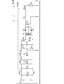
- FIG. 1 is a circuit diagram of a switching power supply device 101 according to the first embodiment and a moving body 301 equipped with this switching power supply device 101.
- FIG. 2 is a diagram showing paths of noise currents flowing through circuits of the switching power supply device 101 according to the first embodiment and a moving body 301 equipped with the switching power supply device 101.
- FIG. FIG. 3 is a circuit diagram of a switching power supply device 102 according to the second embodiment and a moving body 302 equipped with this switching power supply device 102.
- FIG. FIG. 4 is a circuit diagram of a switching power supply device 103A according to the third embodiment and a moving object 303A equipped with this switching power supply device 103A.
- FIG. 5 is a circuit diagram of another switching power supply device 103B according to the third embodiment and a moving body 303B equipped with this switching power supply device 103B.
- FIG. 6 is a diagram showing paths of noise currents flowing through a circuit of a switching power supply device as a comparative example and a moving body provided with this switching power supply device.
- FIG. 1 is a circuit diagram of a switching power supply device 101 according to the first embodiment and a moving body 301 equipped with this switching power supply device 101. As shown in FIG. 1
- a switching power supply device 101 is a power supply device mounted on a moving body 301 having a frame ground 1 electrically insulated from the ground G. This switching power supply device 101 has a noise reduction circuit which will be described later.
- the moving object 301 is, for example, an electric vehicle such as a HV (hybrid vehicle), an EV (electric vehicle), a PHV (plug-in hybrid vehicle), or an FCV (fuel cell vehicle).
- the frame ground is the chassis of the electric vehicle.
- the frame ground 1 of the moving body 301 is electrically insulated from the ground (earth) G by rubber tires.
- a switching power supply device 101 includes a metal housing 2 electrically connected to a frame ground 1, inputs Pin1 and Pin2 of an input power supply PS electrically insulated from the frame ground 1, and a load electrically connected to the frame ground 1. It includes an output section Pout for Lo, and a DC-DC converter that converts power input to the input sections Pin1 and Pin2 into power output to the output section Pout.
- the DC-DC converter includes an input capacitor Ci, switching elements Q1 and Q2, an isolation transformer TR, diodes D1 and D2, and an output smoothing capacitor Co.
- this leakage inductance of the insulating transformer TR occurs in series with the secondary winding, this leakage inductance and the output smoothing capacitor Co form a smoothing circuit. This smoothing circuit smoothes ripples in the output voltage.
- the noise reduction circuit includes an X capacitor Cx, Y capacitors Cy1 and Cy2, a first common mode choke coil CMCC1, and a choke coil CC.
- the X capacitor Cx is connected between the inputs Pin1, Pin2 and the input capacitor Ci.
- the Y capacitors Cy1 and Cy2 are connected between the X capacitor Cx and the input capacitor Ci and electrically connected to the metal housing 2 and the frame ground 1 .
- the first common mode choke coil CMCC1 is connected between the X capacitor Cx and the Y capacitors Cy1 and Cy2, and is connected to the current path between the input parts Pin1 and Pin2 and the input capacitor Ci.
- a choke coil CC is provided in a current path between the output smoothing capacitor Co and the output section Pout.
- the X capacitor Cx corresponds to the first capacitor according to the invention
- the Y capacitors Cy1 and Cy2 correspond to the second capacitors according to the invention.
- the choke coil CC is composed of wiring inductance formed by a current path between the output smoothing capacitor Co and the output section Pout. Therefore, there is no need to mount the choke coil CC as a component, and the size and weight of the switching power supply device 101 can be reduced. Of course, a choke coil CC as a component may be connected to the current path between the output smoothing capacitor Co and the output section Pout.
- the noise reduction circuit, the metal housing 2 and the frame ground 1 form a noise balance circuit.
- the noise balance circuit is a closed circuit against noise currents of noise (common mode noise) generated by the switching operations of the switching elements Q1 and Q2.
- This noise balancing circuit cancels (suppresses) common mode noise generated by the switching operations of the switching elements Q1 and Q2.
- the input power supply PS is, for example, a lithium ion battery, for example, a high voltage battery of about several hundred V (about 200 V to 600 V), and its DC voltage is input to input units Pin1 and Pin2.
- the high voltage is not limited to about several hundred volts, and is a relatively high voltage that cannot be driven by the voltage of the load Lo, such as a motor of a moving body on which the switching power supply device 101 is mounted.
- the switching elements Q1 and Q2 are controlled by a control signal from the switching control circuit, and the switching elements Q1 and Q2 are alternately turned on/off.
- the output voltage of the switching circuit by the switching elements Q1 and Q2 is applied to the primary winding of the isolation transformer TR, and the output current of the switching circuit flows through the primary winding of the isolation transformer TR.
- Diodes D1 and D2 rectify the output current of the secondary winding of isolation transformer TR.
- Diodes D1 and D2 are examples of rectifying elements according to the present invention.
- the output smoothing capacitor Co smoothes the voltage rectified by the diodes D1 and D2.
- the choke coil CC smoothes the current flowing between the output smoothing capacitor Co and the output section Pout.
- the load Lo is, for example, a lead-acid battery, such as a low-voltage battery of about 12V.
- the low voltage is not limited to about 12 V, and is a relatively low voltage that cannot use the voltage of the input power supply PS as it is, such as a car navigation system of a moving body in which the switching power supply device 101 is mounted. be.
- the rectifying elements for rectifying the output of the isolation transformer TR are composed of the diodes D1 and D2, but the rectifying elements are composed of synchronous rectifying elements switched in synchronization with the switching elements Q1 and Q2. You may As a result, loss in the rectifying element can be reduced. For example, when the mobile object 301 is an electric vehicle and the switching power supply device 101 is a DC-DC converter mounted on the electric vehicle, loss in the DC-DC converter can be reduced.
- FIG. 2 is a diagram showing paths of noise currents flowing through circuits of the switching power supply device 101 according to the first embodiment and a moving body 301 equipped with the switching power supply device 101.
- FIG. FIG. 6 is a diagram showing paths of noise currents flowing in circuits of a switching power supply device as a comparative example and a moving body provided with this switching power supply device.
- the input power supply PS is connected to another electronic device 201 that receives power from the input power supply PS.
- Other electronic devices 201 are, for example, inverters and motors that operate at the high voltage.
- the load Lo is a low voltage battery and is connected to another electronic device 202 that receives power from this low voltage battery or from the switching power supply 101 .
- Other electronic equipment 202 is, for example, a car navigation system or a wireless communication device that operates at the low voltage.
- the other electronic device 201 is an inverter or a motor, and is mounted with the frame ground 1 in an electrically insulated state and a thermally conductive state via an insulator sheet.
- a parasitic capacitance Cs1 is generated in the portion interposing the insulator sheet.
- the switching elements Q1 and Q2 are thermally coupled to the metal housing 2 through an insulator sheet in order to dissipate the generated heat to the metal housing 2 and the frame ground 1.
- a parasitic capacitance Cs2 is generated in the portion interposing the insulator sheet.
- a choke coil CC is provided in the current path between the output smoothing capacitor Co and the output part Pout.
- the impedance of the current path passing through this choke coil CC is high. Therefore, the common mode noise current is less likely to pass through this current path, and the noise current reaching the positive electrode of the output section Pout is suppressed. This prevents electromagnetic interference with other electronic devices 202 .
- the self-resonant frequency of the choke coil CC is, for example, 0.53 MHz or more and 108 MHz or less. Therefore, the impedance of the current path in the self-resonant frequency band of the common mode noise current is particularly high, and the noise current reaching the positive electrode of the output section Pout can be effectively suppressed.
- the choke coil CC is not an element for removing common mode noise, but only makes it difficult for noise current to flow in the current path between the output smoothing capacitor Co and the output section Pout, so the impedance of the choke coil CC is Even if it is low, an effect can be obtained, so that the number of turns of the coil can be reduced (there is no need to increase it), and power loss due to copper loss caused by winding of the coil can also be suppressed. Therefore, a decrease in power conversion efficiency can be suppressed.
- the first common mode choke coil CMCC1 Since the first common mode choke coil CMCC1 is provided between the X capacitor Cx and the Y capacitors Cy1 and Cy2, the common mode noise current flowing back to the Y capacitors Cy1 and Cy2 flows through the first common mode choke coil CMCC1. It does not flow to the input sections Pin1 and Pin2.
- the self-resonant frequency of the first common mode choke coil CMCC1 is, for example, 0.53 MHz or more and 108 MHz or less. Therefore, the impedance of the common mode noise current in the self-resonant frequency band is high, and especially the common mode noise current in this frequency band does not return to the input portions Pin1 and Pin2 via the first common mode choke coil CMCC1.
- the choke coil CC, the Y capacitors Cy1 and Cy2, and the first common mode choke coil CMCC1 allow the common mode noise current flowing through the metal housing 2 to return to the switching elements Q1 and Q2, which are noise sources, in the shortest route.
- the noise reduction circuit, the metal housing 2, and the frame ground 1 constitute a noise equalization circuit, and the common mode noise current is balanced within the moving body.
- the path length of the common mode noise current flowing through the metal housing 2 and the frame ground 1 is extremely shortened, suppressing electromagnetic noise radiation from the moving body 301 to the outside.
- the common mode noise current is balanced within the moving body 301, and the radiation of electromagnetic noise to the outside is very effectively suppressed.
- the common mode noise current circulates through the short path described above, the Joule loss due to the flow of the common mode noise current is sufficiently suppressed. Therefore, it is possible to suppress a decrease in the power conversion efficiency of the DC-DC converter.
- FIG. 3 is a circuit diagram of a switching power supply device 102 according to the second embodiment and a moving body 302 equipped with this switching power supply device 102.
- FIG. 3 is a circuit diagram of a switching power supply device 102 according to the second embodiment and a moving body 302 equipped with this switching power supply device 102.
- the switching power supply device 102 is a power supply device mounted on a moving object 302 having a frame ground 1 electrically insulated from the ground G.
- the switching power supply device 102 is electrically connected to the metal housing 2 electrically connected to the frame ground 1, the input parts Pin1 and Pin2 of the input power supply PS electrically isolated from the frame ground 1, and the frame ground 1 It includes an output section Pout to the load Lo and a DC-DC converter that converts power input to the input sections Pin1 and Pin2 into power output to the output section Pout.
- the switching power supply 102 differs from the switching power supply 101 shown in FIG. 1 in that it includes a smoothing coil SC provided between the diodes D1, D2 and the output smoothing capacitor Co.
- This smoothing coil SC smoothes ripples in the output voltage together with the output smoothing capacitor Co.
- a switching power supply device having a different configuration between an input unit and a switching circuit from the example shown in the first embodiment, and a moving body provided with the switching power supply device will be described.
- FIG. 4 is a circuit diagram of a switching power supply device 103A according to the third embodiment and a moving body 303A equipped with this switching power supply device 103A.
- the switching power supply device 103A is a power supply device mounted on a moving object 303A having a frame ground 1 electrically insulated from the ground G.
- the switching power supply 103A is electrically connected to the frame ground 1 with the metal casing 2 electrically connected to the frame ground 1, the input parts Pin1 and Pin2 of the input power supply PS electrically insulated from the frame ground 1, and the frame ground 1. It includes an output section Pout to the load Lo and a DC-DC converter that converts power input to the input sections Pin1 and Pin2 into power output to the output section Pout.
- the switching power supply 103A differs from the switching power supply 101 shown in FIG. 1 in that a second common mode choke coil CMCC2 is provided between the Y capacitors Cy1, Cy2 and the input capacitor Ci. This second common mode choke coil CMCC2 is part of the noise reduction circuit.
- one of the first common mode choke coil CMCC1 and the second common mode choke coil CMCC2 has a self-resonance frequency of 0.53 MHz or more and 1.8 MHz or less, and the other self-resonance frequency is 76 MHz or more and 108 MHz or less.
- the other electronic device 201 connected to the input power supply PS By effectively suppressing the propagation of noise current, electromagnetic interference with other electronic devices 201 can be reduced.
- FIG. 5 is a circuit diagram of another switching power supply device 103B according to the third embodiment and a moving object 303B equipped with this switching power supply device 103B.
- the switching power supply device 103B also has an X capacitor connected between the positive and negative electrodes of the input parts Pin1 and Pin2 between the input parts Pin1 and Pin2 and the input capacitor Ci. Between Cx, the X capacitor Cx and the input capacitor Ci, between the positive terminals of the input sections Pin1 and Pin2 and the metal housing 2 and the frame ground 1, and between the negative terminals of the input sections Pin1 and Pin2 and the metal housing 2 and the frame ground. 1 and Y capacitors Cy1 and Cy2 respectively connected between .
- the switching power supply device 103B shown in FIG. 5 includes a second common mode choke coil CMCC2 between the Y capacitors Cy1, Cy2 and the first common mode choke coil CMCC1.
- CMCC1 and the second common mode choke coil CMCC2 has a self-resonant frequency of 0.53 MHz or more and 1.8 MHz or less, and the other self-resonant frequency of 76 MHz or more and 108 MHz or less. Even with such a configuration, propagation of noise current to other electronic devices 201 connected to the input power supply PS can be effectively suppressed, and electromagnetic interference with other electronic devices 201 can be reduced.
- CC choke coil Ci input capacitor CMCC1 first common mode choke coil CMCC2 second common mode choke coil Co output smoothing capacitors Cs1, Cs2, Cs3 parasitic capacitance Cx X capacitor (first capacitor) Cy1, Cy2...Y capacitor (second capacitor) D1, D2 Diode G Earth ground Lo Load Pin1, Pin2 Input section Pout Output section PS Input power source Q1, Q2 Switching element SC Smoothing coil TR Insulation transformer 1 Frame ground 2 Metal case 101 , 102, 103A, 103B... switching power supply devices 201, 202... electronic devices 301, 302, 303A, 303B... mobile bodies
Landscapes
- Engineering & Computer Science (AREA)
- Power Engineering (AREA)
- Physics & Mathematics (AREA)
- Electromagnetism (AREA)
- Dc-Dc Converters (AREA)
Priority Applications (2)
| Application Number | Priority Date | Filing Date | Title |
|---|---|---|---|
| DE112022001531.4T DE112022001531T5 (de) | 2021-06-28 | 2022-06-22 | Schaltnetzteilvorrichtung |
| JP2023531849A JP7563599B2 (ja) | 2021-06-28 | 2022-06-22 | スイッチング電源装置 |
Applications Claiming Priority (2)
| Application Number | Priority Date | Filing Date | Title |
|---|---|---|---|
| JP2021-106257 | 2021-06-28 | ||
| JP2021106257 | 2021-06-28 |
Publications (1)
| Publication Number | Publication Date |
|---|---|
| WO2023276797A1 true WO2023276797A1 (ja) | 2023-01-05 |
Family
ID=84691735
Family Applications (1)
| Application Number | Title | Priority Date | Filing Date |
|---|---|---|---|
| PCT/JP2022/024790 Ceased WO2023276797A1 (ja) | 2021-06-28 | 2022-06-22 | スイッチング電源装置 |
Country Status (3)
| Country | Link |
|---|---|
| JP (1) | JP7563599B2 (https=) |
| DE (1) | DE112022001531T5 (https=) |
| WO (1) | WO2023276797A1 (https=) |
Cited By (1)
| Publication number | Priority date | Publication date | Assignee | Title |
|---|---|---|---|---|
| WO2025204820A1 (ja) * | 2024-03-28 | 2025-10-02 | ミネベアミツミ株式会社 | 電源装置 |
Citations (3)
| Publication number | Priority date | Publication date | Assignee | Title |
|---|---|---|---|---|
| JP2006280131A (ja) * | 2005-03-30 | 2006-10-12 | Fujitsu Ltd | 電源装置およびデータ処理装置 |
| JP2016158423A (ja) * | 2015-02-25 | 2016-09-01 | 日立オートモティブシステムズ株式会社 | 電力変換装置 |
| JP2020191763A (ja) * | 2019-05-24 | 2020-11-26 | 株式会社デンソー | 電力変換装置 |
Family Cites Families (4)
| Publication number | Priority date | Publication date | Assignee | Title |
|---|---|---|---|---|
| JP5320816B2 (ja) | 2008-05-23 | 2013-10-23 | 株式会社デンソー | 電力変換回路 |
| JP2009296756A (ja) | 2008-06-04 | 2009-12-17 | Denso Corp | 電力変換装置 |
| EP3273585B1 (en) | 2015-03-16 | 2023-04-26 | Mitsubishi Electric Corporation | Power circuit device |
| DE112020005305T5 (de) | 2019-12-17 | 2022-09-15 | Murata Manufacturing Co., Ltd. | Elektronische schaltung |
-
2022
- 2022-06-22 WO PCT/JP2022/024790 patent/WO2023276797A1/ja not_active Ceased
- 2022-06-22 JP JP2023531849A patent/JP7563599B2/ja active Active
- 2022-06-22 DE DE112022001531.4T patent/DE112022001531T5/de active Pending
Patent Citations (3)
| Publication number | Priority date | Publication date | Assignee | Title |
|---|---|---|---|---|
| JP2006280131A (ja) * | 2005-03-30 | 2006-10-12 | Fujitsu Ltd | 電源装置およびデータ処理装置 |
| JP2016158423A (ja) * | 2015-02-25 | 2016-09-01 | 日立オートモティブシステムズ株式会社 | 電力変換装置 |
| JP2020191763A (ja) * | 2019-05-24 | 2020-11-26 | 株式会社デンソー | 電力変換装置 |
Cited By (1)
| Publication number | Priority date | Publication date | Assignee | Title |
|---|---|---|---|---|
| WO2025204820A1 (ja) * | 2024-03-28 | 2025-10-02 | ミネベアミツミ株式会社 | 電源装置 |
Also Published As
| Publication number | Publication date |
|---|---|
| DE112022001531T5 (de) | 2023-12-28 |
| JP7563599B2 (ja) | 2024-10-08 |
| JPWO2023276797A1 (https=) | 2023-01-05 |
Similar Documents
| Publication | Publication Date | Title |
|---|---|---|
| JP7563598B2 (ja) | スイッチング電源装置 | |
| KR20190054390A (ko) | 전기자동차용 충전 및 저전압 변환 복합회로 | |
| US11257616B2 (en) | Power conversion device and high-voltage noise filter | |
| CN107077951A (zh) | 双模扼流圈、使用双模扼流圈的高频滤波器、车载用马达一体型电动助力转向系统及车载用充电装置 | |
| KR102934950B1 (ko) | 충전 장치 | |
| US12609615B2 (en) | Switching power supply device for reducing common mode noise generated by a switching element | |
| JP2012196113A (ja) | 電源装置 | |
| CN112514224B (zh) | 高电压滤波器和电力转换装置 | |
| JP7563599B2 (ja) | スイッチング電源装置 | |
| Saket et al. | Common-mode noise elimination in planar transformers for LLC resonant converters | |
| US11312245B2 (en) | Vehicle power supply system | |
| KR20160046416A (ko) | 노이즈 보상 회로 | |
| US11565595B2 (en) | Filter circuit arrangement, an electric vehicle and a method of operating an electric vehicle | |
| US20250292970A1 (en) | Capacitive winding of a dc link capacitor and dc link capacitor with a common-mode current leakage function | |
| KR102938746B1 (ko) | 스위칭 회로 및 전원 장치 | |
| CN112693320A (zh) | 具有交错式可变电压转换器的汽车电驱动系统 | |
| US20240333170A1 (en) | Power conversion circuit and power supply device | |
| JP2003309902A (ja) | 車両用電力変換装置 | |
| JP3972344B2 (ja) | 車両用電力変換装置 | |
| CN107768826A (zh) | 机动车的天线单元与能量耦合装置的电磁脱耦 | |
| JP2022007010A (ja) | パワーユニット | |
| JP2020129865A (ja) | 送電装置 | |
| JP2006230196A (ja) | 車両用電力変換装置 | |
| JP2014023307A (ja) | 車載用電力変換装置 | |
| JP2017005860A (ja) | 電力変換装置 |
Legal Events
| Date | Code | Title | Description |
|---|---|---|---|
| 121 | Ep: the epo has been informed by wipo that ep was designated in this application |
Ref document number: 22832945 Country of ref document: EP Kind code of ref document: A1 |
|
| WWE | Wipo information: entry into national phase |
Ref document number: 112022001531 Country of ref document: DE |
|
| WWE | Wipo information: entry into national phase |
Ref document number: 2023531849 Country of ref document: JP |
|
| 122 | Ep: pct application non-entry in european phase |
Ref document number: 22832945 Country of ref document: EP Kind code of ref document: A1 |