WO2023248337A1 - フィルム、巻回体、接続構造体、及び接続構造体の製造方法 - Google Patents
フィルム、巻回体、接続構造体、及び接続構造体の製造方法 Download PDFInfo
- Publication number
- WO2023248337A1 WO2023248337A1 PCT/JP2022/024681 JP2022024681W WO2023248337A1 WO 2023248337 A1 WO2023248337 A1 WO 2023248337A1 JP 2022024681 W JP2022024681 W JP 2022024681W WO 2023248337 A1 WO2023248337 A1 WO 2023248337A1
- Authority
- WO
- WIPO (PCT)
- Prior art keywords
- film
- adhesive
- adhesive film
- pieces
- groove
- Prior art date
- Legal status (The legal status is an assumption and is not a legal conclusion. Google has not performed a legal analysis and makes no representation as to the accuracy of the status listed.)
- Ceased
Links
Images










Classifications
-
- C—CHEMISTRY; METALLURGY
- C09—DYES; PAINTS; POLISHES; NATURAL RESINS; ADHESIVES; COMPOSITIONS NOT OTHERWISE PROVIDED FOR; APPLICATIONS OF MATERIALS NOT OTHERWISE PROVIDED FOR
- C09J—ADHESIVES; NON-MECHANICAL ASPECTS OF ADHESIVE PROCESSES IN GENERAL; ADHESIVE PROCESSES NOT PROVIDED FOR ELSEWHERE; USE OF MATERIALS AS ADHESIVES
- C09J7/00—Adhesives in the form of films or foils
- C09J7/40—Adhesives in the form of films or foils characterised by release liners
- C09J7/403—Adhesives in the form of films or foils characterised by release liners characterised by the structure of the release feature
-
- B—PERFORMING OPERATIONS; TRANSPORTING
- B32—LAYERED PRODUCTS
- B32B—LAYERED PRODUCTS, i.e. PRODUCTS BUILT-UP OF STRATA OF FLAT OR NON-FLAT, e.g. CELLULAR OR HONEYCOMB, FORM
- B32B27/00—Layered products comprising a layer of synthetic resin
-
- B—PERFORMING OPERATIONS; TRANSPORTING
- B32—LAYERED PRODUCTS
- B32B—LAYERED PRODUCTS, i.e. PRODUCTS BUILT-UP OF STRATA OF FLAT OR NON-FLAT, e.g. CELLULAR OR HONEYCOMB, FORM
- B32B3/00—Layered products comprising a layer with external or internal discontinuities or unevennesses, or a layer of non-planar shape; Layered products comprising a layer having particular features of form
- B32B3/26—Layered products comprising a layer with external or internal discontinuities or unevennesses, or a layer of non-planar shape; Layered products comprising a layer having particular features of form characterised by a particular shape of the outline of the cross-section of a continuous layer; characterised by a layer with cavities or internal voids ; characterised by an apertured layer
- B32B3/266—Layered products comprising a layer with external or internal discontinuities or unevennesses, or a layer of non-planar shape; Layered products comprising a layer having particular features of form characterised by a particular shape of the outline of the cross-section of a continuous layer; characterised by a layer with cavities or internal voids ; characterised by an apertured layer characterised by an apertured layer, the apertures going through the whole thickness of the layer, e.g. expanded metal, perforated layer, slit layer regular cells B32B3/12
-
- B—PERFORMING OPERATIONS; TRANSPORTING
- B32—LAYERED PRODUCTS
- B32B—LAYERED PRODUCTS, i.e. PRODUCTS BUILT-UP OF STRATA OF FLAT OR NON-FLAT, e.g. CELLULAR OR HONEYCOMB, FORM
- B32B3/00—Layered products comprising a layer with external or internal discontinuities or unevennesses, or a layer of non-planar shape; Layered products comprising a layer having particular features of form
- B32B3/26—Layered products comprising a layer with external or internal discontinuities or unevennesses, or a layer of non-planar shape; Layered products comprising a layer having particular features of form characterised by a particular shape of the outline of the cross-section of a continuous layer; characterised by a layer with cavities or internal voids ; characterised by an apertured layer
- B32B3/30—Layered products comprising a layer with external or internal discontinuities or unevennesses, or a layer of non-planar shape; Layered products comprising a layer having particular features of form characterised by a particular shape of the outline of the cross-section of a continuous layer; characterised by a layer with cavities or internal voids ; characterised by an apertured layer characterised by a layer formed with recesses or projections, e.g. hollows, grooves, protuberances, ribs
-
- B—PERFORMING OPERATIONS; TRANSPORTING
- B32—LAYERED PRODUCTS
- B32B—LAYERED PRODUCTS, i.e. PRODUCTS BUILT-UP OF STRATA OF FLAT OR NON-FLAT, e.g. CELLULAR OR HONEYCOMB, FORM
- B32B7/00—Layered products characterised by the relation between layers; Layered products characterised by the relative orientation of features between layers, or by the relative values of a measurable parameter between layers, i.e. products comprising layers having different physical, chemical or physicochemical properties; Layered products characterised by the interconnection of layers
- B32B7/04—Interconnection of layers
- B32B7/06—Interconnection of layers permitting easy separation
-
- C—CHEMISTRY; METALLURGY
- C09—DYES; PAINTS; POLISHES; NATURAL RESINS; ADHESIVES; COMPOSITIONS NOT OTHERWISE PROVIDED FOR; APPLICATIONS OF MATERIALS NOT OTHERWISE PROVIDED FOR
- C09J—ADHESIVES; NON-MECHANICAL ASPECTS OF ADHESIVE PROCESSES IN GENERAL; ADHESIVE PROCESSES NOT PROVIDED FOR ELSEWHERE; USE OF MATERIALS AS ADHESIVES
- C09J7/00—Adhesives in the form of films or foils
-
- C—CHEMISTRY; METALLURGY
- C09—DYES; PAINTS; POLISHES; NATURAL RESINS; ADHESIVES; COMPOSITIONS NOT OTHERWISE PROVIDED FOR; APPLICATIONS OF MATERIALS NOT OTHERWISE PROVIDED FOR
- C09J—ADHESIVES; NON-MECHANICAL ASPECTS OF ADHESIVE PROCESSES IN GENERAL; ADHESIVE PROCESSES NOT PROVIDED FOR ELSEWHERE; USE OF MATERIALS AS ADHESIVES
- C09J7/00—Adhesives in the form of films or foils
- C09J7/30—Adhesives in the form of films or foils characterised by the adhesive composition
-
- C—CHEMISTRY; METALLURGY
- C09—DYES; PAINTS; POLISHES; NATURAL RESINS; ADHESIVES; COMPOSITIONS NOT OTHERWISE PROVIDED FOR; APPLICATIONS OF MATERIALS NOT OTHERWISE PROVIDED FOR
- C09J—ADHESIVES; NON-MECHANICAL ASPECTS OF ADHESIVE PROCESSES IN GENERAL; ADHESIVE PROCESSES NOT PROVIDED FOR ELSEWHERE; USE OF MATERIALS AS ADHESIVES
- C09J9/00—Adhesives characterised by their physical nature or the effects produced, e.g. glue sticks
- C09J9/02—Electrically-conducting adhesives
-
- H—ELECTRICITY
- H01—ELECTRIC ELEMENTS
- H01R—ELECTRICALLY-CONDUCTIVE CONNECTIONS; STRUCTURAL ASSOCIATIONS OF A PLURALITY OF MUTUALLY-INSULATED ELECTRICAL CONNECTING ELEMENTS; COUPLING DEVICES; CURRENT COLLECTORS
- H01R11/00—Individual connecting elements providing two or more spaced connecting locations for conductive members which are, or may be, thereby interconnected, e.g. end pieces for wires or cables supported by the wire or cable and having means for facilitating electrical connection to some other wire, terminal, or conductive member, blocks of binding posts
- H01R11/01—Individual connecting elements providing two or more spaced connecting locations for conductive members which are, or may be, thereby interconnected, e.g. end pieces for wires or cables supported by the wire or cable and having means for facilitating electrical connection to some other wire, terminal, or conductive member, blocks of binding posts characterised by the form or arrangement of the conductive interconnection between the connecting locations
-
- B—PERFORMING OPERATIONS; TRANSPORTING
- B32—LAYERED PRODUCTS
- B32B—LAYERED PRODUCTS, i.e. PRODUCTS BUILT-UP OF STRATA OF FLAT OR NON-FLAT, e.g. CELLULAR OR HONEYCOMB, FORM
- B32B2307/00—Properties of the layers or laminate
- B32B2307/20—Properties of the layers or laminate having particular electrical or magnetic properties, e.g. piezoelectric
- B32B2307/202—Conductive
-
- B—PERFORMING OPERATIONS; TRANSPORTING
- B32—LAYERED PRODUCTS
- B32B—LAYERED PRODUCTS, i.e. PRODUCTS BUILT-UP OF STRATA OF FLAT OR NON-FLAT, e.g. CELLULAR OR HONEYCOMB, FORM
- B32B2307/00—Properties of the layers or laminate
- B32B2307/70—Other properties
- B32B2307/732—Dimensional properties
- B32B2307/737—Dimensions, e.g. volume or area
- B32B2307/7375—Linear, e.g. length, distance or width
- B32B2307/7376—Thickness
-
- B—PERFORMING OPERATIONS; TRANSPORTING
- B32—LAYERED PRODUCTS
- B32B—LAYERED PRODUCTS, i.e. PRODUCTS BUILT-UP OF STRATA OF FLAT OR NON-FLAT, e.g. CELLULAR OR HONEYCOMB, FORM
- B32B2405/00—Adhesive articles, e.g. adhesive tapes
Definitions
- the present invention relates to a film, a wound body, a connected structure, and a method for manufacturing a connected structure.
- the adhesive forming the adhesive film piece is not completely cured, it tends to deform and spread along the surface of the release film over time.
- the film since the film is wound around the core by applying a predetermined tension to the release film, the film is in a state of being pressurized toward the core (center) in the wound body. This pressing force is also called winding pressure because it is generated by winding the film. The winding pressure increases toward the center. Therefore, the adhesive film pieces sandwiched between the inner layer side (the core side) and the outer layer side (the side opposite to the core side) by the release film are pressed from the inner layer side and the outer layer side by the release film, and the release film The object tries to deform itself so that it is pushed out along the surface of the object.
- the adhesive film pieces When the adhesive film pieces are deformed so as to be spread out along the surface of the release film, the adhesive film pieces tend to protrude from the adhesive surface, resulting in poor yield.
- the adhesive that forms the adhesive film pieces contains a liquid component resin, the deformation of the adhesive film pieces along the surface of the release film becomes noticeable, resulting in a reduction in yield. It's likely to get worse.
- one aspect of the present invention is to provide a film, a wound body, a connected structure, and a method for manufacturing a connected structure that can suppress the spread of adhesive film pieces.
- the inventors of the present invention have conducted extensive studies on the above-mentioned problems, and have found that by forming grooves on the surface of the release film piece and making the width of the groove a predetermined value or more, it is possible to suppress the spread of the adhesive film piece. I learned that it is possible.
- the present invention has been made based on the above findings.
- the film according to one aspect of the present invention includes a long release film, a plurality of adhesive film pieces provided on the release film, and a plurality of adhesive film pieces formed on the surface of one side of the release film. a groove extending along the outer edge of each of the pieces of adhesive film, the width of the groove being greater than or equal to 15 ⁇ m.
- the release film is provided with a groove formed on one surface of the plurality of adhesive film pieces and extending along the outer edge of each of the plurality of adhesive film pieces, and the width of the groove is 15 ⁇ m or more. Therefore, by preventing each of the plurality of adhesive film pieces from spreading along the surface of the release film by the groove, it is possible to suppress each of the plurality of adhesive film pieces from spreading beyond the groove. .
- the groove may be located on the outside of the outer edge of each of the plurality of adhesive film pieces.
- the groove since the groove is located outside the outer edge of each of the plurality of adhesive film pieces, it is possible to further suppress the spread of each of the plurality of adhesive film pieces.
- the depth of the groove may be 10% or more of the thickness of the release film.
- the width of the groove can be easily made to be 15 ⁇ m or more, and each of the plurality of adhesive film pieces can cross the groove. The route for this can be made longer. Thereby, it is possible to further suppress each of the plurality of adhesive film pieces from spreading beyond the groove.
- the depth of the groove may be 85% or less of the thickness of the release film. In this film, since the depth of the groove is 85% or less of the thickness of the release film, breakage of the release film can be suppressed.
- the depth of the groove may be 20% or more of the thickness of the adhesive film piece surrounded by the groove among the plurality of adhesive film pieces.
- the depth of the groove is 20% or more of the thickness of the adhesive film piece surrounded by the groove, so that the path for each of the plurality of adhesive film pieces to cross the groove can be lengthened. . Thereby, it is possible to further suppress each of the plurality of adhesive film pieces from spreading beyond the groove.
- the depth of the groove may be 100% or less of the thickness of the adhesive film piece surrounded by the groove among the plurality of adhesive film pieces.
- the grooves can be easily formed because the depth of the grooves is 100% or less of the thickness of the adhesive film piece surrounded by the grooves.
- the adhesive forming each of the plurality of adhesive film pieces may have a multilayer structure.
- each of the plurality of adhesive film pieces can spread easily.
- the groove has a width of 15 ⁇ m or more, it is possible to suppress each of the plurality of adhesive film pieces from spreading beyond the groove.
- the degree of curing of the adhesive forming each of the plurality of adhesive film pieces as measured by differential scanning calorimetry may be 80% or more at 150° C. for 10 seconds.
- the degree of curing of the adhesive forming each of the plurality of adhesive film pieces is 80% or more as determined by differential scanning calorimetry at 150°C for 10 seconds, thereby preventing the effects of heat on areas other than the connection points. Can be made smaller.
- the plurality of adhesive film pieces may be spaced apart from each other.
- the adhesive film pieces since the plurality of adhesive film pieces are spaced apart from each other, the adhesive film pieces can be attached to the adhesive surface without affecting adjacent adhesive film pieces. This allows the adhesive film piece to be easily attached to the adhesive surface.
- the plurality of adhesive film pieces may be spaced apart from the edge of the release film in the width direction of the release film.
- the adhesive since the plurality of adhesive film pieces are spaced apart from the edge of the release film in the width direction of the release film, when the edge of the release film interferes with another member, the adhesive can be removed from the release film. Peeling of the film pieces can be suppressed.
- the plurality of adhesive film pieces may be arranged in a line in the longitudinal direction of the release film.
- the adhesive film pieces since the plurality of adhesive film pieces are arranged in a line in the longitudinal direction of the release film, the adhesive film pieces can be easily attached.
- At least one of the plurality of adhesive film pieces may have a hole.
- at least one of the plurality of adhesive film pieces has a hole, so that, for example, the adhesive film piece can be applied appropriately to the central part where there is a part where it is not desired to paste the adhesive film piece. Can be attached.
- the plurality of adhesive film pieces may have the same shape. With this film, multiple pieces of adhesive film have the same shape, allowing the pieces of adhesive film to be efficiently attached to multiple adhesive surfaces with the same shape, either consecutively or simultaneously. .
- the adhesive film piece may have electrical conductivity.
- the adhesive film piece since the adhesive film piece has electrical conductivity, two members connected via the adhesive film piece can be electrically connected.
- the adhesive film piece may contain conductive particles.
- the adhesive film pieces since the adhesive film pieces contain conductive particles, conductivity can be easily imparted to the adhesive film pieces.
- a wound body according to one aspect of the present invention includes any of the above films and a core around which the film is wound.
- one of the above-mentioned films is wound around the winding core, so a winding pressure is applied to the film toward the winding core (center). Therefore, the adhesive film pieces sandwiched between the inner layer side (the core side) and the outer layer side (the side opposite to the core side) by the release film are pressed from the inner layer side and the outer layer side by the release film, and the release film The object tries to deform itself so that it is pushed out along the surface of the object.
- the film is provided with grooves formed on one surface of the plurality of adhesive films of the release film and extending along the outer edges of each of the plurality of adhesive film pieces, and the width of the groove is 15 ⁇ m or more. Therefore, by preventing each of the plurality of adhesive film pieces from spreading along the surface of the release film by the groove, it is possible to suppress each of the plurality of adhesive film pieces from spreading beyond the groove. .
- a connection structure includes a first member having a first bonding surface, a second member having a second bonding surface, and any of the above connecting structures that connect the first bonding surface and the second bonding surface. and a piece of adhesive film.
- a method for manufacturing a connected structure includes a preparation step of preparing any of the films described above, and bonding the first adhesive surface of the first member and the second member via the adhesive film piece of the film. and a connecting step of connecting the second adhesive surface.
- the adhesive film It is possible to manufacture a connected structure in which protrusion of the pieces from the first member and the second member is suppressed.
- FIG. 1 is a plan view showing a part of the film according to the present embodiment.
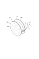
- FIG. 2 is a perspective view showing the wound body according to this embodiment.
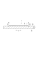
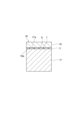
- FIG. 3 is a cross-sectional view showing an example of a cross section taken along line III-III shown in FIG.
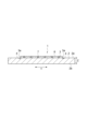
- FIG. 4 is a sectional view showing another example of the cross section taken along line III-III shown in FIG.
- FIG. 5 is a sectional view showing another example of the cross section taken along the line III--III shown in FIG.
- FIG. 6 is a plan view showing another example of a part of the film.
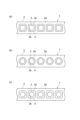
- FIGS. 7(a), 7(b), and 7(c) are plan views showing other examples of part of the film.
- FIG. 8 is a plan view showing another example of a part of the film.
- FIG. 9 is a plan view showing another example of a part of the film.
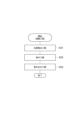
- FIG. 10 is a flowchart showing a method for manufacturing a film according to an embodiment.
- 11(a), FIG. 11(b), FIG. 11(c), and FIG. 11(d) are cross-sectional views for explaining the method of manufacturing the film shown in FIG. 1.
- 12(a), FIG. 12(b), FIG. 12(c), and FIG. 12(d) are perspective views for explaining the method for manufacturing the film shown in FIG. 1.
- FIG. 13 is a sectional view showing the connected structure according to this embodiment.
- FIG. 14 is a flowchart showing a method for manufacturing a connected structure according to this embodiment.
- FIG. 15 is a flowchart showing the connection process shown in FIG. 14.
- FIG. 14 is a flowchart showing the connection process shown in FIG. 14.
- FIG. 16 is a schematic process diagram for explaining the connection process shown in FIG. 14.
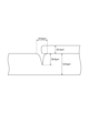
- FIG. 17 is a schematic diagram of the observation surface of Example 1.
- FIG. 18 is a schematic diagram of the observation surface of Example 2.
- FIG. 19 is a schematic diagram of the observation surface of Example 3.
- FIG. 20 is a schematic diagram of the observation surface of Example 4.
- FIG. 21 is a schematic diagram of the observation surface of Comparative Example 1.
- FIG. 22 is a table showing the observation results of Examples 1 to 4 and Comparative Example 1.
- the film 1 includes a long (tape-shaped) release film 2, a plurality of adhesive film pieces 3 provided on the release film 2, and a plurality of adhesive films of the release film 2.
- a groove 4 (see FIGS. 3 to 5) formed on the surface 2a of the piece 3 and extending along the outer edge 3a of each of the plurality of adhesive film pieces 3 is provided. Note that, as shown in FIG. 2, the film 1 is stored, transported, etc. as a roll 15 wound around a core 14.
- the release film 2 is attached to the plurality of adhesive film pieces 3 and supports the plurality of adhesive film pieces 3.
- the material for the release film for example, polyethylene terephthalate (PET), polyethylene, polypropylene, etc. can be used.
- PET polyethylene terephthalate
- the release film 2 may contain any filler.
- the surface of the release film 2 may be subjected to a release treatment, a plasma treatment, an antistatic treatment, or the like.
- the release film 2 may be provided with an alignment mark for specifying the position of the adhesive film piece 3 on the film 1, and the position of the adhesive film piece 3 may be specified based on this alignment mark.
- the position of the adhesive film piece 3 on the film 1 may be specified by detecting a specific arrangement of the adhesive film piece 3 on the film 1. Therefore, it is conceivable to detect the position of the adhesive film piece 3 on the film 1 using the imaging device 33 (see FIG. 16).
- the imaging device 33 considering that the adhesive film piece 3 is subsequently attached to the adhesive surface, it is preferable to arrange the imaging device 33 on the opposite side of the adhesive film piece 3 to the release film 2.
- the release film 2 may have light transparency so that the position of the adhesive film piece 3 can be detected from the release film 2 side by the imaging device 33.
- the transmittance of the release film 2 can be 15% or more and 100% or less, preferably 15% or more and 99% or less, and more preferably 16% or more and 98% or less.
- the transmittance of the release film 2 can be measured as follows. A release film cut into a square of 50 mm x 50 mm is set in a haze meter (for example, NDH-5000 manufactured by Nippon Denshoku Industries Co., Ltd.), and the total light transmittance is measured. Then, this measurement result is defined as the transmittance of the release film 2.
- a haze meter for example, NDH-5000 manufactured by Nippon Denshoku Industries Co., Ltd.
- the haze value of the release film 2 can be 3% or more and 100% or less, preferably 3% or more and 99% or less, and more preferably 4% or more and 99% or less.
- the haze value of the release film 2 can be measured as follows. A release film cut into a square of 50 mm x 50 mm is set in a haze meter (for example, NDH-5000 manufactured by Nippon Denshoku Industries Co., Ltd.), and the haze value is measured. Then, this measurement result is defined as the haze value of the release film 2.
- a haze meter for example, NDH-5000 manufactured by Nippon Denshoku Industries Co., Ltd.
- each of the plurality of adhesive film pieces 3 (hereinafter also simply referred to as "adhesive film pieces 3") connects a first member and a second member to be bonded.
- the adhesive film pieces 3 may have the same thickness in order to facilitate a good connection.
- the adhesive film piece 3 may also have a flat surface in order to facilitate a good connection. That is, the surface of the adhesive film piece 3 on the release film 2 side and the surface of the adhesive film piece 3 on the opposite side to the release film 2 may be flat.
- the same thickness includes not only completely the same thickness but also a thickness error of about ⁇ 10%.
- a flat surface includes not only a completely flat surface but also an error in flatness of approximately ⁇ 10%.
- the adhesive film piece 3 has a film-like adhesive 6. As shown in FIGS.
- the adhesive 6 forming the adhesive film piece 3 can have a multilayer structure, for example.
- the multilayer structure includes, for example, a structure in which adhesive films with different components are coated on top of each other, a structure in which separate adhesive films are bonded together, and the like.
- thermoplastic resin for example, a thermoplastic resin, a thermosetting resin, a mixed system of a thermoplastic resin and a thermosetting resin, or a photocuring resin
- thermoplastic resin for example, a styrene resin type or a polyester resin type is used.
- thermosetting resin for example, an epoxy resin type, an acrylic resin type, or a silicone resin type is used.
- heating and pressurization are usually required. In the case of thermoplastic resins, this is to flow the resin to obtain adhesion to the adherend, and in the case of thermosetting resins, this is to further perform a curing reaction of the resin.
- photocurable resins do not require heating for curing, they are useful when low-temperature connections are required.
- the adhesive 6 forming the adhesive film piece 3 has a curing degree of 150° C. for 10 seconds as measured by differential scanning calorimetry (DSC), for example, from the viewpoint of minimizing the influence of heat on areas other than the connection points. 80% or more at 160°C for 10 seconds, 80% or more at 170°C for 10 seconds, 80% or more at 180°C for 10 seconds, 80% or more at 200°C for 10 seconds , 80% or more at 210° C. for 10 seconds, or 80% or more at 230° C. for 10 seconds.
- the optimum resin properties can be selected depending on the reliability level required for the final device.
- the degree of curing measured by differential scanning calorimetry is calculated by using a differential scanning calorimeter (for example, DSC Q-2500 manufactured by TA Instruments) to determine the residual calorific value of the cured resin relative to the calorific value of the uncured resin. It can be calculated from the difference between
- the adhesive film piece 3 may be conductive or non-conductive.
- the adhesive film piece 3 may be formed of a conductive adhesive film or a non-conductive adhesive film, and the adhesive film piece 3 may be formed of a conductive adhesive film or a non-conductive adhesive film.
- a hybrid adhesive film having a region and a non-conductive adhesive region may be formed.
- the adhesive film piece 3 may be composed of two layers, a first adhesive layer and a second adhesive layer, and the first adhesive layer, the second adhesive layer, and the third adhesive layer. It may be composed of three or more layers.
- the first adhesive layer, the second adhesive layer, and the third adhesive layer may be conductive or non-conductive.
- the conductive adhesive film forming the adhesive film piece 3 may have isotropic conductivity or anisotropic conductivity, for example.
- conductivity can be easily achieved by containing conductive particles 7.
- the conductive particles 7 are contained in the adhesive 6, for example.
- the conductive particles 7 for example, metal particles such as Au, Ag, Ni, Cu, Pd, and solder, and carbon particles are used. Further, the conductive particles 7 may be formed by coating the surface of a transition metal such as Ni or Cu with a noble metal such as Au, Ag or Pd. Further, the conductive particles 7 may be formed by forming a conductive layer on the surface of a non-conductive particle such as glass, ceramic, plastic, etc. by coating the surface of the non-conductive particle with a conductive substance. The conductive particles 7 may also have an outermost layer made of noble metals, or may use heat-melting metal particles.
- the conductive particles 7 may be conductive particles having an isotropic shape such as a substantially spherical shape, for example.
- the conductive particles having an isotropic shape refer to, for example, conductive particles having a shape that is approximately point symmetrical. From the viewpoint of achieving good connection characteristics even when an oxide film is formed on the electrode surface of the member to be connected, the conductive particles 7 may be, for example, dendrite-like (also called dendritic), flake-like (flat plate, scaly), etc.
- the conductive particles may have an anisotropic shape, such as a shape (also called a shape).
- the conductive particles having an anisotropic shape are, for example, conductive particles having shape anisotropy and not having a shape that is approximately point symmetric (isotropic shape). Since the conductive particles 7 have an anisotropic shape, they can penetrate the oxide film on the electrode surface and achieve good connection characteristics.
- the conductive particles 7 may be used singly or in combination of two or more.
- the hybrid adhesive film forming the adhesive film piece 3 has a conductive adhesive region 8 and a non-conductive adhesive region 9 arranged adjacently on the release film 2. It may be something like that.
- the conductive adhesive region 8 may, for example, contain conductive particles 7 similarly to the conductive adhesive film.
- the plurality of adhesive film pieces 3 may be spaced apart in the longitudinal direction X of the release film 2, or may be connected in the longitudinal direction X of the release film 2. As shown in FIG. 1, in this embodiment, the plurality of adhesive film pieces 3 are spaced apart in the longitudinal direction X of the release film 2. However, like the film 1 shown in FIG. 6, the plurality of adhesive film pieces 3 may be connected in the longitudinal direction X of the release film 2.
- the separation distance in the longitudinal direction X of the adjacent adhesive film pieces 3 can be 0.1 mm or more and 20 mm or less, and 0. .1 mm or more and 15 mm or less, 0.1 mm or more and 10 mm or less, 0.1 mm or more and 8 mm or less, or 0.2 mm or more and 5 mm or less.
- the distance between adjacent adhesive film pieces 3 in the longitudinal direction At the same time, it is possible to effectively utilize the film 1 and reduce costs.
- the shape of the adhesive film piece 3 is not particularly limited, and can be made into various shapes.
- the shape of the adhesive film piece 3 includes circles such as perfect circles and ellipses, polygons such as triangles and squares, star shapes, and complex shapes such as various marks.
- Examples of the quadrilateral include a square, a rectangle, and a trapezoid.
- the adhesive film piece 3 may have holes 3b.
- the hole 3b is formed by hollowing out (punching) a part of the adhesive film piece 3.
- the shape, size, position, number, etc. of the holes 3b are not particularly limited.
- the hole 3b may have a similar shape to the adhesive film piece 3, or may not have a similar shape to the adhesive film piece 3.
- Examples of the shape of the hole 3b include circles such as perfect circles and ellipses, polygons such as triangles and quadrangles, star shapes, and complex shapes such as various marks.
- Examples of the quadrilateral include a square, a rectangle, and a trapezoid.
- the position of the hole 3b may be at the center of the adhesive film piece 3 or at the end of the adhesive film piece 3.
- the number of holes 3b formed in one adhesive film piece 3 may be one, or two or more. When a plurality of holes 3b are formed in one adhesive film piece 3, the shape, size, etc. of each hole 3b may be the same or different.
- the adhesive film piece 3 shown in FIG. 7(a) has a rectangular outer shape, and a rectangular hole 3b similar to the outer shape of the adhesive film piece 3 is formed in the center thereof.
- the adhesive film piece 3 has a circular outer shape, and a circular hole 3b similar to the outer shape of the adhesive film piece 3 is formed in the center thereof.
- the adhesive film piece 3 shown in FIG. 7(c) has a square outer shape, and a circular square hole 3b is formed in the center thereof.
- the plurality of adhesive film pieces 3 may be arranged in one row in the longitudinal direction X of the release film 2, or may be arranged in multiple rows in the longitudinal direction X of the release film 2. Note that when a plurality of adhesive film pieces 3 are arranged in a line in the longitudinal direction X of the release film 2, only the plurality of adhesive film pieces 3 arranged in this line are provided on the release film 2. ing.
- the plurality of adhesive film pieces 3 are arranged in a line in the longitudinal direction X of the release film 2, the plurality of adhesive film pieces 3 are arranged in a line in the width direction They may be arranged at the center of the release film 2, or may be arranged at positions shifted (offset) from the center of the release film 2 in the width direction Y, as in the film 1 shown in FIG.
- the plurality of adhesive film pieces 3 may have the same shape, or may have different shapes like the film 1 shown in FIG. 9. When the plurality of adhesive film pieces 3 have different shapes, all the adhesive film pieces 3 may have different shapes from each other, and some adhesive film pieces 3 have mutually different shapes and adhesive film pieces 3 have the same shape. may be mixed.
- the plurality of adhesive film pieces 3 may be spaced apart from the edge of the release film 2 in the width direction Y of the release film 2.
- the distance between the edge of the release film 2 in the width direction Y of the release film 2 and the adhesive film piece 3 closest to the edge can be 0.1 mm or more and 20 mm or less, and 0.1 mm or more. It may be greater than or equal to 15 mm, may be greater than or equal to 0.1 mm and less than or equal to 10 mm, may be greater than or equal to 0.1 mm and less than or equal to 8 mm, and may be greater than or equal to 0.2 mm and less than or equal to 5 mm.
- the groove 4 is formed on the surface 2a of the release film 2 on the side of the plurality of adhesive film pieces 3, and the groove 4 is formed on the surface 2a of the release film 2 on the side of the plurality of adhesive film pieces 3. does not reach the back surface 2b on the opposite side. That is, the grooves 4 extend from the surface 2a of the release film 2 to the film 1 perpendicularly to the longitudinal direction It is recessed in the thickness direction Z.
- the groove 4 is also called a half-cut line.
- the groove 4 may extend in a solid line shape or in a broken line shape.
- the groove 4 extending in a solid line shape means that the groove 4 extends continuously without interruption.
- the expression that the groove 4 extends in a broken line shape means that the groove 4 is partially interrupted at one or more locations, and thus extends discontinuously.
- the part where the groove 4 is partially interrupted is also referred to as a break in the groove 4.
- the cuts in the groove 4 may be formed at predetermined intervals or may be formed at arbitrary positions.
- the grooves 4 are formed on the surface 2a of the release film 2 in order to prevent each of the plurality of adhesive film pieces 3 from spreading along the surface 2a of the release film 2. Further, the width (line width) of the groove 4 is 15 ⁇ m or more.
- the width of the groove 4 is the width on the surface 2a of the release film 2, and is the width in the direction perpendicular to the extending direction of the groove 4. Note that since the grooves 4 extend along the outer edges 3a of each of the plurality of adhesive film pieces 3, the direction in which the grooves 4 extend differs depending on the position where the grooves 4 are formed. Therefore, the width of the groove 4 is the width in the direction perpendicular to the extending direction of the groove 4 at the point where the groove 4 is formed.
- the width of the groove 4 is preferably 20 ⁇ m or more.
- the width of the grooves 4 is preferably 50 ⁇ m or less, more preferably 45 ⁇ m or less, and even more preferably 40 ⁇ m or less. From these viewpoints, the width of the groove 4 is preferably 15 ⁇ m or more and 50 ⁇ m or less, more preferably 15 ⁇ m or more and 45 ⁇ m or less, and even more preferably 20 ⁇ m or more and 40 ⁇ m or less.
- the groove 4 may be located at a position overlapping the outer edge 3a of each of the plurality of adhesive film pieces 3, or may be located outside the outer edge 3a of each of the plurality of adhesive film pieces 3.
- the groove 4 has substantially the same shape as each of the plurality of adhesive film pieces 3, that is, the same or slightly larger shape as each of the plurality of adhesive film pieces 3, in a plan view of the film 1.
- the plane view of the film 1 refers to the case viewed from the surface direction of the release film 2 (the direction perpendicular to the surface 2a of the release film 2), as shown in FIG. Note that FIGS. 3 to 5 show the case where the groove 4 is located outside the outer edge 3a of each of the plurality of adhesive film pieces 3.
- the depth of the groove 4 is not particularly limited, and can be set as appropriate within a range that does not penetrate the release film 2.
- the depth of the groove 4 is the depth in the thickness direction Z of the film 1.
- the depth of the grooves 4 is determined by the release film 2. It is preferably 10% or more of the thickness of the release film 2, more preferably 20% or more of the thickness of the release film 2, and still more preferably 30% or more of the thickness of the release film 2.
- the depth of the groove 4 is preferably 85% or less of the thickness of the release film 2, and preferably 80% or less of the thickness of the release film 2. It is more preferable that the thickness be 75% or less of the thickness of the release film 2. From these viewpoints, the depth of the groove 4 is preferably 10% or more and 85% or less of the thickness of the release film 2, and more preferably 20% or more and 80% or less of the thickness of the release film 2. More preferably, the thickness is 30% or more and 75% or less of the thickness of the release film 2.
- the depth of the groove 4 is determined by the amount of adhesive surrounded by the groove 4 of the plurality of adhesive film pieces 3. It is preferably 20% or more of the thickness of the film piece 3, more preferably 30% or more of the thickness of the adhesive film piece 3 surrounded by the groove 4 among the plurality of adhesive film pieces 3, More preferably, the thickness is 40% or more of the thickness of the adhesive film piece 3 surrounded by the groove 4 among the plurality of adhesive film pieces 3.
- the depth of the groove 4 is 100% or less of the thickness of the adhesive film piece 3 surrounded by the groove 4 among the plurality of adhesive film pieces 3.
- the thickness is preferably 90% or less of the thickness of the adhesive film piece 3 surrounded by the groove 4 of the plurality of adhesive film pieces 3, and the thickness of the adhesive film piece 3 surrounded by the groove 4 of the plurality of adhesive film pieces 3 is preferably 90% or less. It is more preferable that the thickness is 80% or less of the thickness of the adhesive film piece 3 surrounded by 4. From these viewpoints, the depth of the groove 4 is preferably 20% or more and 100% or less of the thickness of the adhesive film piece 3 surrounded by the groove 4 among the plurality of adhesive film pieces 3; More preferably, the thickness is 30% or more and 90% or less of the thickness of the adhesive film piece 3 surrounded by the groove 4 of the adhesive film piece 3, and surrounded by the groove 4 of the plurality of adhesive film pieces 3.
- the thickness is 40% or more and 80% or less of the thickness of the adhesive film piece 3.
- the thickness of the adhesive film piece 3 is the thickness in the thickness direction Z of the film 1, similar to the depth of the groove 4.
- the groove 4 extends along the outer edge 3a of each of the plurality of adhesive film pieces 3, each of the plurality of adhesive film pieces 3 is surrounded by the groove 4. Therefore, when one adhesive film piece 3 is the target adhesive film piece and the groove 4 extending along the outer edge 3a of the target adhesive film piece is the target groove, the groove of the plurality of adhesive film pieces 3 is The adhesive film piece 3 surrounded by 4 becomes the target adhesive film piece surrounded by the target groove.
- the film manufacturing method includes, for example, an adhesive film layer forming step (S11), an adhesive film layer cutting step (S12) performed after the adhesive film layer forming step (S11), and an adhesive film layer cutting step (S12) performed after the adhesive film layer forming step (S11).
- a margin peeling step (S13) is performed after the agent film layer cutting step (S12).
- a release film 2 is prepared.
- an adhesive film layer 3A is formed on the entire surface of the release film 2.
- the adhesive film layer 3A is a layer that becomes a plurality of adhesive film pieces 3.
- the adhesive film layer 3A is formed of, for example, an adhesive 6 and conductive particles 7 contained in the adhesive 6.
- the adhesive 6 and conductive particles 7 forming the adhesive film layer 3A are the same as the adhesive 6 and conductive particles 7 forming the adhesive film piece 3 described above.
- the adhesive film layer cutting step (S12) along the outer edge line 3B forming the outer edge 3a of the plurality of adhesive film pieces 3 provided on the film 1,
- the adhesive film layer 3A formed on the release film 2 is cut, and the release film 2 is also half-cut.
- Cutting of the adhesive film layer 3A and half-cutting of the release film 2 are performed, for example, by pressing the adhesive film layer 3A against a roll cutter having a cutting blade formed on the outer peripheral surface.
- a cutting blade for example, a Pinnacle (registered trademark) blade, a Thomson blade, etc. can be used.
- Half-cutting the release film 2 means cutting the surface 2a of the release film 2 on the adhesive film layer 3A side so that the back surface 2b of the release film 2 on the opposite side to the adhesive film layer 3A is not cut. .
- cutting lines along the outer edges 3a of the plurality of adhesive film pieces 3 provided on the film 1 are formed in the adhesive film layer 3A, and cutting lines along the respective outer edges 3a of the plurality of adhesive film pieces 3 provided on the film 1 are formed in the release film 2.
- a half-cut line is formed along the outer edge 3a of each film piece 3.
- the release film 2 is half-cut so that the width of the half-cut line of the release film 2 is 15 ⁇ m or more.
- the width of the half-cut line of the release film 2 can be set to 15 ⁇ m or more.
- the adhesive film layer 3A is separated into an inner portion 3A1 located inside the outer edge line 3B and a plurality of blank portions 3A2 located outside the outer edge line 3B.
- the inner portion 3A1 is a portion that becomes a plurality of adhesive film pieces 3 provided on the film 1.
- the margin portion 3A2 is a portion other than the plurality of adhesive film pieces 3 provided on the film 1.
- the margin portion 3A2 of the adhesive film layer 3A is peeled from the release film 2 along the cut outer edge line 3B. .
- the margin portion 3A2 is peeled off by, for example, adhering an adhesive tape to the margin portion 3A2, pulling the adhesive tape, and peeling off the margin portion 3A2 from the release film 2.
- the inner portion 3A1 remaining on the release film 2 becomes a plurality of adhesive film pieces 3 provided on the film 1.
- the film 1 in which the plurality of adhesive film pieces 3 are provided on the release film 2 is manufactured.
- the half-cut line of the release film 2 becomes a groove 4 formed on the surface 2a of the release film 2 on the side of the plurality of adhesive film pieces 3 and extending along the outer edge 3a of each of the plurality of adhesive film pieces 3. . Therefore, in the film 1 manufactured in this way, grooves 4 are formed on the surface 2a of the release film 2 on the side of the plurality of adhesive film pieces 3 and extend along the outer edges 3a of each of the plurality of adhesive film pieces 3. is formed, and the width of the groove 4 is 15 ⁇ m or more.
- the rolled body 15 includes a long (tape-shaped) film 1 and a core 14 around which the film 1 is wound. That is, the wound body 15 is formed by winding the film 1 around the winding core 14.
- the winding core 14 includes a core material 14a and a pair of side plates 14b.
- the core material 14a is formed in a cylindrical shape.
- the film 1 is wound around the outer peripheral surface of the core material 14a.
- the pair of side plates 14b are attached to both ends of the core material 14a in the axial direction.
- a pair of side plates 14b support the film 1 from left and right sides. The distance between the pair of side plates 14b is slightly wider than the width of the film 1.
- connection structure 16 includes a first member 17 having a first adhesive surface 17a, a second member 18 having a second adhesive surface 18a, and a first adhesive surface 17a and a second adhesive surface 18a. and an adhesive film piece 3 for connecting the two.
- the first member 17 includes, for example, chip components such as IC chips, LSI chips, resistor chips, and capacitor chips, photoelectric conversion components such as LEDs and image sensors, piezoelectric conversion components such as strain sensors, pressure sensors, acoustic components, and piezo elements. parts, circuit forming parts such as flexible printed wiring boards, thermal sensors such as thermometers and heat sinks, and thermal management parts.
- chip components such as IC chips, LSI chips, resistor chips, and capacitor chips
- photoelectric conversion components such as LEDs and image sensors
- piezoelectric conversion components such as strain sensors, pressure sensors, acoustic components, and piezo elements.
- parts circuit forming parts such as flexible printed wiring boards
- thermal sensors such as thermometers and heat sinks
- thermal management parts thermal management parts.
- the surface facing the second member 18 is a first adhesive surface 17a.
- a first electrode (not shown) for electrical connection with the second member 18 is arranged on the first adhesive surface 17a.
- the second member 18 is, for example, a glass substrate, a polyimide substrate, a polyamideimide substrate, a polyethylene terephthalate substrate, a polycarbonate substrate, a cycloolefin polymer (COP) substrate, a polyethylene naphthalate substrate, a glass reinforced epoxy substrate, a paper phenol substrate, a ceramic substrate. , a substrate having optical transparency such as a laminate, and a silicon substrate.
- the surface facing the first adhesive surface 17a of the first member 17 is a second adhesive surface 18a.
- a second electrode (not shown) for electrical connection with the first member 17 is arranged on the second adhesive surface 18a.
- first member 17 and the second member 18, and any member may be applied to each member.
- the adhesive film piece 3 is the adhesive film piece 3 peeled off from the film 1 described above.
- the adhesive film piece 3 connects the first adhesive surface 17a and the second adhesive surface 18a by means of the adhesive 6.
- the adhesive film piece 3 has anisotropic conductivity due to the conductive particles 7, the conductive particles 7 conduct the first electrode on the first adhesive surface 17a and the second electrode on the second adhesive surface 18a. can be done.
- the method for manufacturing a connected structure includes a preparation step (S21) and a connection step (S22) performed after the preparation step (S21).
- the film 1 described above is prepared.
- a wound body 15 in which the film 1 is wound is prepared as the film 1.
- the above-described film manufacturing method may be performed, or only the film 1 manufactured by the above-described film manufacturing method may be prepared.
- connection step (S22) includes a position detection step (S31), an attaching step (S32), and an overlapping step (S33).
- the film 1 is unwound from the roll 15. Then, as shown in FIG. 16, the position of the adhesive film piece 3 on the film 1 is detected by the imaging device 33.
- the imaging device 33 may be placed on the adhesive film piece 3 side with respect to the release film 2, or may be placed on the opposite side of the adhesive film piece 3 with respect to the release film 2.
- the imaging device 33 is arranged on the opposite side of the adhesive film piece 3 to the release film 2. In this case, by using the light-transmitting release film 2, the imaging device 33 can detect the position of the adhesive film piece 3 on the film 1 from the release film 2 side.
- the adhesive film piece 3 is pasted on the first adhesive surface 17a based on the position detected in the position detecting step (S31). Thereafter, the release film 2 is peeled off from the adhesive film piece 3 attached to the first adhesive surface 17a.
- the adhesive film piece 3 can be easily peeled off from the release film 2 by applying heat and pressure within a range that does not affect the degree of curing of the adhesive in the adhesive film piece 3.
- the heating temperature may be 70° C.
- the heating time may be 1 second
- the pressure may be 1 MPa relative to the area of the adhesive film piece 3.
- the first adhesive surface 17a and the second adhesive surface 18a are overlapped with the adhesive film piece 3 interposed therebetween.
- the first adhesive surface 17a and the second adhesive surface 18a are temporarily connected by the adhesive 6 of the adhesive film piece 3.
- the adhesive 6 is cured.
- a connected structure 16 in which the first adhesive surface 17a and the second adhesive surface 18a are connected by the adhesive film piece 3 is obtained.
- the adhesive film piece 3 has anisotropic conductivity due to the inclusion of conductive particles 7, the first member 17 and the second member 18 are pressurized before the adhesive 6 is cured.
- the first member 17 and the second member 18 are electrically connected by the conductive particles 7 of No. 3. In this way, the connected structure 16 is manufactured.
- the release film 2 is provided with a groove 4 formed on the surface 2a on the side of the plurality of adhesive film pieces 3 and extending along the outer edge 3a of each of the plurality of adhesive film pieces 3, and the width of the groove 4 is 15 ⁇ m or more. It is. Therefore, the grooves 4 prevent each of the plurality of adhesive film pieces 3 from spreading along the surface 2a of the release film 2, thereby preventing each of the plurality of adhesive film pieces 3 from spreading beyond the grooves 4. can be suppressed.
- the depth of the groove 4 is 10% or more of the thickness of the release film 2, so that the width of the groove 4 can be easily made 15 ⁇ m or more, and a plurality of adhesive film pieces can be formed. 3 can lengthen the path for crossing the groove 4. Thereby, it is possible to further suppress each of the plurality of adhesive film pieces 3 from spreading beyond the grooves 4.
- the depth of the grooves 4 is 85% or less of the thickness of the release film 2, so that breakage of the release film 2 can be suppressed.
- the depth of the groove 4 is 20% or more of the thickness of the adhesive film piece 3 surrounded by the groove 4, so that each of the plurality of adhesive film pieces 3 can exceed the groove 4.
- the route can be made longer. Thereby, it is possible to further suppress each of the plurality of adhesive film pieces 3 from spreading beyond the grooves 4.
- the grooves 4 can be easily formed because the depth of the grooves 4 is 100% or less of the thickness of the adhesive film piece 3 surrounded by the grooves 4.
- each of the plurality of adhesive film pieces 3 since the adhesive 6 forming each of the plurality of adhesive film pieces 3 has a multilayer structure, each of the plurality of adhesive film pieces 3 can easily spread. However, as described above, since the groove 4 has a width of 15 ⁇ m or more, it is possible to suppress each of the plurality of adhesive film pieces 3 from spreading beyond the groove 4.
- the degree of curing of the adhesive 6 forming each of the plurality of adhesive film pieces 3 measured by differential scanning calorimetry is 80% or more at 150°C for 10 seconds, and 80% or more at 160°C for 10 seconds. % or more, 80% or more at 170°C for 10 seconds, 80% or more at 180°C for 10 seconds, 80% or more at 200°C for 10 seconds, 80% or more at 210°C for 10 seconds, or 230°C
- 80% or more under the condition of 10 seconds it is possible to reduce the influence of heat on areas other than the connection points, and to appropriately suppress each of the plurality of adhesive film pieces 3 from spreading beyond the grooves 4. can do.
- the adhesive 6 forming each of the plurality of adhesive film pieces 3 is made of thermoplastic resin such as styrene resin, polyester resin, epoxy resin, acrylic resin, silicone resin, etc.
- thermoplastic resin such as styrene resin, polyester resin, epoxy resin, acrylic resin, silicone resin, etc.
- thermosetting resin a mixed system of these thermoplastic resins and thermosetting resins, and a photocuring resin, it is possible to appropriately suppress each of the plurality of adhesive film pieces 3 from spreading beyond the grooves 4. be able to.
- the plurality of adhesive film pieces 3 are arranged in a line in the longitudinal direction X of the release film 2, so that the adhesive film pieces 3 can be easily pasted.
- At least one of the plurality of adhesive film pieces 3 has the hole 3b, so that, for example, it is possible to appropriately attach the adhesive film piece 3 to a central part of the area where the adhesive film piece 3 is not desired.
- a piece of adhesive film 3 can be applied.
- the adhesive film pieces 3 since the plurality of adhesive film pieces 3 have the same shape, the adhesive film pieces 3 can be efficiently attached to a plurality of adhesive surfaces having the same shape.
- the adhesive film piece 3 contains the conductive particles 7, conductivity can be easily imparted to the adhesive film piece 3.
- the film 1 since the film 1 described above is wound around the winding core 14, the film 1 has a winding that is pressed toward the core material 14a (center) of the winding core 14. There is pressure. Therefore, the adhesive film piece 3 sandwiched between the release film 2 from the inner layer side (the core side) and the outer layer side (the side opposite to the core) is pressed by the release film 2 from the inner layer side and the outer layer side. , the release film 2 tries to deform so as to be spread out along the surface 2a.
- the film 1 is provided with a groove 4 formed on the surface 2a of the release film 2 on the side of the plurality of adhesive film pieces 3 and extending along the outer edge 3a of each of the plurality of adhesive film pieces 3.
- the width is 15 ⁇ m or more. Therefore, the grooves 4 prevent each of the plurality of adhesive film pieces 3 from spreading along the surface 2a of the release film 2, thereby preventing each of the plurality of adhesive film pieces 3 from spreading beyond the grooves 4. can be suppressed.
- the first member 17 and the second member 18 are connected by the adhesive film piece 3, so the first member 17 and the second member of the adhesive film piece 3 are It is possible to obtain the connection structure 16 in which protrusion from the member 18 is suppressed.
- the first adhesive surface 17a of the first member 17 and the second adhesive surface 18a of the second member 18 are connected via the adhesive film piece 3 of the film 1 described above. Because of the connection, it is possible to manufacture a connected structure 16 in which protrusion of the adhesive film piece 3 from the first member 17 and the second member 18 is suppressed.
- the connecting step includes using a film and connecting the first member and the second member with an adhesive film piece of the film. It may be realized by any method as long as it is possible.
- the film is described as having a two-layer structure in which a plurality of adhesive film pieces are provided on a release film, but a second release film is further provided on a plurality of adhesive film pieces. It may also have a three-layer structure with
- the film according to [1] or [2], wherein the depth of the groove is 10% or more of the thickness of the release film.
- the depth of the groove is 20% or more of the thickness of the adhesive film piece surrounded by the groove among the plurality of adhesive film pieces. film. [6] According to any one of [1] to [5], the depth of the groove is 100% or less of the thickness of the adhesive film piece surrounded by the groove among the plurality of adhesive film pieces. film. [7] The film according to any one of [1] to [6], wherein the adhesive forming each of the plurality of adhesive film pieces has a multilayer structure. [8] The degree of curing of the adhesive forming each of the plurality of adhesive film pieces according to differential scanning calorimetry is 80% or more at 150° C. for 10 seconds, according to any one of [1] to [7].
- a method for manufacturing a connected structure comprising: a connecting step of connecting surfaces.
- Example 1 An adhesive film layer containing an adhesive and conductive particles was formed on the entire surface of the long release film. Next, the adhesive film layer formed on the release film is cut along the outer edge line forming the outer edge of the plurality of adhesive film pieces provided on the film using a roll cutter having a pinnacle blade formed on the outer peripheral surface. The release film was cut in half. Next, a margin portion of the adhesive film layer other than the plurality of adhesive film pieces provided on the film was peeled off from the release film along the cut outline. Thereby, a plurality of adhesive film pieces are provided on the release film, and a groove is formed on the surface of one side of the plurality of adhesive film pieces of the release film and extends along the outer edge of each of the plurality of adhesive film pieces.
- the film of Example 1 was obtained. Then, a wound body was prepared by winding the film of Example 1 around a core with a tension of 1.5N, the film was unwound from the wound body, the film was cut at an arbitrary position, and the cut surface was observed. Images were taken using a scanning electron microscope as a surface. As the scanning electron microscope, S8020 manufactured by Hitachi High-Tech Corporation was used. A schematic diagram of the captured image is shown in FIG.
- the width of the groove is 25.8 ⁇ m
- the depth of the groove is 28.6 ⁇ m
- the thickness of the release film is 53.6 ⁇ m
- the ratio of the depth of the groove to the thickness of the release film. was 53%
- the thickness of the adhesive film piece was 20.4 ⁇ m.
- Example 2 A film of Example 2 was obtained in the same manner as in Example 1.
- a roll body was prepared by winding the film of Example 2 around a core, the film was unwound from the roll body, the film was cut at an arbitrary position, and the cut Images were taken with a scanning electron microscope using the surface as the observation surface. A schematic diagram of the captured image is shown in FIG.
- the width of the groove is 30.5 ⁇ m
- the depth of the groove is 40.8 ⁇ m
- the thickness of the release film is 52.4 ⁇ m
- the ratio of the depth of the groove to the thickness of the release film. was 78%
- the thickness of the adhesive film piece was 21.3 ⁇ m.
- Example 3 A film of Example 3 was obtained in the same manner as in Example 1.
- a roll body was prepared by winding the film of Example 3 around a core, the film was unwound from the roll body, the film was cut at an arbitrary position, and the cut Images were taken with a scanning electron microscope using the surface as the observation surface. A schematic diagram of the captured image is shown in FIG.
- the width of the groove is 34.6 ⁇ m
- the depth of the groove is 51.6 ⁇ m
- the thickness of the release film is 62.9 ⁇ m
- the ratio of the depth of the groove to the thickness of the release film. was 82%
- the thickness of the adhesive film piece was 28.3 ⁇ m.
- Example 4 A film of Example 4 was obtained in the same manner as in Example 1.
- a roll body was prepared by winding the film of Example 4 around a core, the film was unwound from the roll body, the film was cut at an arbitrary position, and the cut Images were taken with a scanning electron microscope using the surface as the observation surface. A schematic diagram of the captured image is shown in FIG.
- the width of the groove is 35.0 ⁇ m
- the depth of the groove is 52.4 ⁇ m
- the thickness of the release film is 59.5 ⁇ m
- the ratio of the depth of the groove to the thickness of the release film. was 88%
- the thickness of the adhesive film piece was 29.4 ⁇ m.
- Comparative example 1 A film of Comparative Example 1 was obtained in the same manner as in Example 1.
- a rolled body was prepared by winding the film of Comparative Example 1 around a core, the film was unwound from the rolled body, the film was cut at an arbitrary position, and the cut Images were taken with a scanning electron microscope using the surface as the observation surface. A schematic diagram of the captured image is shown in FIG.
- the width of the groove is 11.0 ⁇ m
- the depth of the groove is 4.37 ⁇ m
- the thickness of the release film is 50.2 ⁇ m
- the ratio of the depth of the groove to the thickness of the release film. was 9%
- the thickness of the adhesive film piece was 26.4 ⁇ m.
- Example 4 where the ratio of the groove depth to the thickness of the release film was greater than 85%, the release film was broken, but when the ratio of the groove depth to the thickness of the release film was 85% or less, In Examples 1 to 3, the release film was not broken. Therefore, it is presumed that breakage of the release film can be suppressed by setting the ratio of the depth of the groove to the thickness of the release film to 85% or less.
- the present invention can be used, for example, as a film, a wound body, a connected structure, and a method for manufacturing a connected structure.
Landscapes
- Chemical & Material Sciences (AREA)
- Organic Chemistry (AREA)
- Adhesive Tapes (AREA)
Abstract
Description
図1に示すように、フィルム1は、長尺の(テープ状の)剥離フィルム2と、剥離フィルム2上に設けられた複数の接着剤フィルム片3と、剥離フィルム2の複数の接着剤フィルム片3側の表面2aに形成されて複数の接着剤フィルム片3のそれぞれの外縁3aに沿って延びる溝4(図3~図5参照)と、を備える。なお、フィルム1は、図2に示すように、巻芯14に巻回された巻回体15として保管、運搬等される。
剥離フィルム2は、複数の接着剤フィルム片3に貼り付けられて、複数の接着剤フィルム片3を支持する。剥離フィルム2の素材は、例えば、ポリエチレンテレフタレート(PET)、ポリエチレン、ポリプロピレン等を用いることができる。剥離フィルム2には、任意の充填剤を含有させてもよい。また、剥離フィルム2の表面には、離型処理、プラズマ処理、静電防止処理等が施されていてもよい。
複数の接着剤フィルム片3のそれぞれ(以下、単に「接着剤フィルム片3」ともいう)は、接着対象である第一部材と第二部材とを接続する。このため、良好な接続を容易にする観点から、接着剤フィルム片3は、同一の厚さを有していてもよい。また、良好な接続を容易にする観点から、接着剤フィルム片3は、平坦な表面を有していてもよい。つまり、接着剤フィルム片3の剥離フィルム2側の表面及び接着剤フィルム片3の剥離フィルム2とは反対側の表面が、平坦となっていてもよい。同一の厚さとは、完全に同一の厚さのほか、±10%程度の厚さの誤差を含む意味である。また、平坦な表面とは、完全に平坦な表面のほか、±10%程度の平坦度の誤差を含む意味である。図3~図5に示すように、接着剤フィルム片3は、フィルム状の接着剤6を有する。
図1及び図3~図5に示すように、溝4は、剥離フィルム2の複数の接着剤フィルム片3側の表面2aに形成されており、剥離フィルム2の複数の接着剤フィルム片3とは反対側の裏面2bには至っていない。つまり、溝4は、剥離フィルム2の複数の接着剤フィルム片3とは反対側の裏面2bに到達しないように、剥離フィルム2の表面2aから、長手方向X及び幅方向Yと直交するフィルム1の厚さ方向Zに凹んでいる。溝4は、ハーフカット線とも呼ばれる。
図10に示すように、フィルムの製造方法は、例えば、接着剤フィルム層形成工程(S11)と、接着剤フィルム層形成工程(S11)の後に行う接着剤フィルム層切断工程(S12)と、接着剤フィルム層切断工程(S12)の後に行う余白剥離工程(S13)と、を備える。
図2に示すように、巻回体15は、長尺の(テープ状の)フィルム1と、フィルム1が巻回された巻芯14と、を備える。つまり、巻回体15は、巻芯14にフィルム1が巻回されてなる。
図13に示すように、接続構造体16は、第一接着面17aを有する第一部材17と、第二接着面18aを有する第二部材18と、第一接着面17aと第二接着面18aとを接続する接着剤フィルム片3と、を備える。
図14に示すように、接続構造体の製造方法は、準備工程(S21)と、準備工程(S21)の後に行う接続工程(S22)と、を備える。
長尺の剥離フィルムと、前記剥離フィルム上に設けられた複数の接着剤フィルム片と、前記剥離フィルムの前記複数の接着剤フィルム片側の表面に形成されて前記複数の接着剤フィルム片のそれぞれの外縁に沿って延びる溝と、を備え、前記溝の幅は、15μm以上である、フィルム。
[2]
前記溝は、前記複数の接着剤フィルム片のそれぞれの前記外縁の外側に位置している、[1]に記載のフィルム。
[3]
前記溝の深さは、前記剥離フィルムの厚さの10%以上である、[1]又は[2]に記載のフィルム。
[4]
前記溝の深さは、前記剥離フィルムの厚さの85%以下である、[1]~[3]の何れか一つに記載のフィルム。
[5]
前記溝の深さは、前記複数の接着剤フィルム片のうちの前記溝に囲まれる接着剤フィルム片の厚さの20%以上である、[1]~[4]の何れか一つに記載のフィルム。
[6]
前記溝の深さは、前記複数の接着剤フィルム片のうちの前記溝に囲まれる接着剤フィルム片の厚さの100%以下である、[1]~[5]の何れか一つに記載のフィルム。
[7]
前記複数の接着剤フィルム片のそれぞれを形成する接着剤は、多層構造を有する、[1]~[6]の何れか一つに記載のフィルム。
[8]
前記複数の接着剤フィルム片のそれぞれを形成する接着剤の示差走査熱量測定の硬化度は、150℃10秒の条件で80%以上である、[1]~[7]の何れか一つに記載のフィルム。
[9]
前記複数の接着剤フィルム片は、互いに離間している、[1]~[8]の何れか一つに記載のフィルム。
[10]
前記複数の接着剤フィルム片は、前記剥離フィルムの幅方向における前記剥離フィルムの端縁から離間している、[1]~[9]の何れか一つに記載のフィルム。
[11]
前記複数の接着剤フィルム片は、前記剥離フィルムの長手方向に一列に配列されている、[1]~[10]の何れか一つに記載のフィルム。
[12]
前記複数の接着剤フィルム片の少なくとも一つは、穴を有する、
[1]~[11]の何れか一つに記載のフィルム。
[13]
前記複数の接着剤フィルム片は、同じ形をしている、[1]~[12]の何れか一つに記載のフィルム。
[14]
前記接着剤フィルム片は、導電性を有する、[1]~[13]の何れか一つに記載のフィルム。
[15]
前記接着剤フィルム片は、導電粒子を含有する、[14]に記載のフィルム。
[16]
[1]~[15]の何れか一つに記載のフィルムと、前記フィルムが巻回された巻芯と、を備える、巻回体。
[17]
第一接着面を有する第一部材と、第二接着面を有する第二部材と、前記第一接着面と前記第二接着面とを接続する[1]~[15]の何れか一つに記載の接着剤フィルム片と、を備える、接続構造体。
[18]
[1]~[15]の何れか一つに記載のフィルムを準備する準備工程と、前記フィルムの前記接着剤フィルム片を介して第一部材の第一接着面と第二部材の第二接着面とを接続する接続工程と、を備える、接続構造体の製造方法。
次に、本発明の実施例について説明する。但し、本発明は、以下の実施例に限定されるものではない。
長尺の剥離フィルム上の全面に、接着剤及び導電粒子を含有する接着剤フィルム層を形成した。次に、外周面にピナクル刃が形成されたロールカッターにより、フィルムに設ける複数の接着剤フィルム片の外縁を成す外縁線に沿って、剥離フィルム上に形成された接着剤フィルム層を切断するとともに剥離フィルムをハーフカットした。次に、切断された外形線に沿って、接着剤フィルム層のうち、フィルムに設ける複数の接着剤フィルム片以外の部分となる余白部分を、剥離フィルムから剥離した。これにより、剥離フィルム上に複数の接着剤フィルム片が設けられるとともに、剥離フィルムの複数の接着剤フィルム片側の表面に形成されて複数の接着剤フィルム片のそれぞれの外縁に沿って延びる溝が形成された、実施例1のフィルムを得た。そして、実施例1のフィルムを1.5Nの張力で巻芯に巻回した巻回体を作製し、巻回体からフィルムを巻き出し、任意の位置でフィルムを切断し、この切断面を観察面として走査型電子顕微鏡で撮像した。走査型電子顕微鏡は、株式会社日立ハイテク製のS8020を用いた。撮像画像の模式図を図17に示す。
実施例1と同様の方法で、実施例2のフィルムを得た。また、実施例1と同様の方法で、実施例2のフィルムを巻芯に巻回した巻回体を作製し、巻回体からフィルムを巻き出し、任意の位置でフィルムを切断し、この切断面を観察面として走査型電子顕微鏡で撮像した。撮像画像の模式図を図18に示す。
実施例1と同様の方法で、実施例3のフィルムを得た。また、実施例1と同様の方法で、実施例3のフィルムを巻芯に巻回した巻回体を作製し、巻回体からフィルムを巻き出し、任意の位置でフィルムを切断し、この切断面を観察面として走査型電子顕微鏡で撮像した。撮像画像の模式図を図19に示す。
実施例1と同様の方法で、実施例4のフィルムを得た。また、実施例1と同様の方法で、実施例4のフィルムを巻芯に巻回した巻回体を作製し、巻回体からフィルムを巻き出し、任意の位置でフィルムを切断し、この切断面を観察面として走査型電子顕微鏡で撮像した。撮像画像の模式図を図20に示す。
実施例1と同様の方法で、比較例1のフィルムを得た。また、実施例1と同様の方法で、比較例1のフィルムを巻芯に巻回した巻回体を作製し、巻回体からフィルムを巻き出し、任意の位置でフィルムを切断し、この切断面を観察面として走査型電子顕微鏡で撮像した。撮像画像の模式図を図21に示す。
図22に示すように、溝の幅が15μm未満となる比較例1では、接着剤フィルム片は溝を越えて広がっていたが、溝の幅が15μm以上となる実施例1~4では、接着剤フィルム片は溝を越えて広がっていなかった。このため、溝の幅を15μm以上とすることで、接着剤フィルム片が溝を越えて広がるのを抑制できることが推察される。
Claims (18)
- 長尺の剥離フィルムと、
前記剥離フィルム上に設けられた複数の接着剤フィルム片と、
前記剥離フィルムの前記複数の接着剤フィルム片側の表面に形成されて前記複数の接着剤フィルム片のそれぞれの外縁に沿って延びる溝と、を備え、
前記溝の幅は、15μm以上である、
フィルム。 - 前記溝は、前記複数の接着剤フィルム片のそれぞれの前記外縁の外側に位置している、
請求項1に記載のフィルム。 - 前記溝の深さは、前記剥離フィルムの厚さの10%以上である、
請求項1又は2に記載のフィルム。 - 前記溝の深さは、前記剥離フィルムの厚さの85%以下である、
請求項3に記載のフィルム。 - 前記溝の深さは、前記複数の接着剤フィルム片のうちの前記溝に囲まれる接着剤フィルム片の厚さの20%以上である、
請求項1又は2に記載のフィルム。 - 前記溝の深さは、前記複数の接着剤フィルム片のうちの前記溝に囲まれる接着剤フィルム片の厚さの100%以下である、
請求項5に記載のフィルム。 - 前記複数の接着剤フィルム片のそれぞれを形成する接着剤は、多層構造を有する、
請求項1又は2に記載のフィルム。 - 前記複数の接着剤フィルム片のそれぞれを形成する接着剤の示差走査熱量測定の硬化度は、150℃10秒の条件で80%以上である、
請求項1又は2に記載のフィルム。 - 前記複数の接着剤フィルム片は、互いに離間している、
請求項1又は2に記載のフィルム。 - 前記複数の接着剤フィルム片は、前記剥離フィルムの幅方向における前記剥離フィルムの端縁から離間している、
請求項1又は2に記載のフィルム。 - 前記複数の接着剤フィルム片は、前記剥離フィルムの長手方向に一列に配列されている、
請求項1又は2に記載のフィルム。 - 前記複数の接着剤フィルム片の少なくとも一つは、穴を有する、
請求項1又は2に記載のフィルム。 - 前記複数の接着剤フィルム片は、同じ形をしている、
請求項1又は2に記載のフィルム。 - 前記接着剤フィルム片は、導電性を有する、
請求項1又は2に記載のフィルム。 - 前記接着剤フィルム片は、導電粒子を含有する、
請求項14に記載のフィルム。 - 請求項1又は2に記載のフィルムと、
前記フィルムが巻回された巻芯と、を備える、
巻回体。 - 第一接着面を有する第一部材と、
第二接着面を有する第二部材と、
前記第一接着面と前記第二接着面とを接続する請求項1又は2に記載の接着剤フィルム片と、を備える、
接続構造体。 - 請求項1又は2に記載のフィルムを準備する準備工程と、
前記フィルムの前記接着剤フィルム片を介して第一部材の第一接着面と第二部材の第二接着面とを接続する接続工程と、を備える、
接続構造体の製造方法。
Priority Applications (6)
| Application Number | Priority Date | Filing Date | Title |
|---|---|---|---|
| US18/859,940 US20250282120A1 (en) | 2022-06-21 | 2022-06-21 | Film, wound body, connection structure, and method for manufacturing connection structure |
| KR1020247041478A KR20250027649A (ko) | 2022-06-21 | 2022-06-21 | 필름, 권회체, 접속 구조체, 및 접속 구조체의 제조 방법 |
| JP2024528142A JPWO2023248337A1 (ja) | 2022-06-21 | 2022-06-21 | |
| PCT/JP2022/024681 WO2023248337A1 (ja) | 2022-06-21 | 2022-06-21 | フィルム、巻回体、接続構造体、及び接続構造体の製造方法 |
| CN202280095538.8A CN119403894A (zh) | 2022-06-21 | 2022-06-21 | 膜、卷绕体、连接结构体及连接结构体的制造方法 |
| TW112123105A TW202406745A (zh) | 2022-06-21 | 2023-06-20 | 膜、捲繞體、連接結構體及連接結構體之製造方法 |
Applications Claiming Priority (1)
| Application Number | Priority Date | Filing Date | Title |
|---|---|---|---|
| PCT/JP2022/024681 WO2023248337A1 (ja) | 2022-06-21 | 2022-06-21 | フィルム、巻回体、接続構造体、及び接続構造体の製造方法 |
Publications (1)
| Publication Number | Publication Date |
|---|---|
| WO2023248337A1 true WO2023248337A1 (ja) | 2023-12-28 |
Family
ID=89379500
Family Applications (1)
| Application Number | Title | Priority Date | Filing Date |
|---|---|---|---|
| PCT/JP2022/024681 Ceased WO2023248337A1 (ja) | 2022-06-21 | 2022-06-21 | フィルム、巻回体、接続構造体、及び接続構造体の製造方法 |
Country Status (6)
| Country | Link |
|---|---|
| US (1) | US20250282120A1 (ja) |
| JP (1) | JPWO2023248337A1 (ja) |
| KR (1) | KR20250027649A (ja) |
| CN (1) | CN119403894A (ja) |
| TW (1) | TW202406745A (ja) |
| WO (1) | WO2023248337A1 (ja) |
Citations (4)
| Publication number | Priority date | Publication date | Assignee | Title |
|---|---|---|---|---|
| JP2006111727A (ja) * | 2004-10-14 | 2006-04-27 | Hitachi Chem Co Ltd | 接着シート及びその製造方法、並びに、半導体装置の製造方法及び半導体装置 |
| WO2015059944A1 (ja) * | 2013-10-21 | 2015-04-30 | リンテック株式会社 | 樹脂膜形成用シート |
| WO2018066411A1 (ja) * | 2016-10-03 | 2018-04-12 | 日立化成株式会社 | 導電性フィルム、巻回体、接続構造体、及び接続構造体の製造方法 |
| WO2019058429A1 (ja) * | 2017-09-19 | 2019-03-28 | 日立化成株式会社 | 半導体装置製造用接着フィルム及びその製造方法 |
Family Cites Families (6)
| Publication number | Priority date | Publication date | Assignee | Title |
|---|---|---|---|---|
| JPH10292159A (ja) * | 1997-04-21 | 1998-11-04 | Nichiban Co Ltd | 剥離ライナ−付粘着テ−プ及び剥離ライナ−並びに剥離ライナ−付粘着テ−プの製造方法 |
| US6524881B1 (en) * | 2000-08-25 | 2003-02-25 | Micron Technology, Inc. | Method and apparatus for marking a bare semiconductor die |
| JP4614126B2 (ja) * | 2005-02-21 | 2011-01-19 | リンテック株式会社 | 積層シート、積層シートの巻取体およびそれらの製造方法 |
| JP5546985B2 (ja) * | 2010-07-28 | 2014-07-09 | 日東電工株式会社 | 半導体装置製造用フィルム、半導体装置製造用フィルムの製造方法、及び、半導体装置の製造方法。 |
| JP6011067B2 (ja) * | 2011-08-12 | 2016-10-19 | 日立化成株式会社 | 粘着フィルム |
| JP5998730B2 (ja) * | 2011-09-16 | 2016-09-28 | 日立化成株式会社 | 粘着フィルム及び粘着フィルムの製造方法 |
-
2022
- 2022-06-21 US US18/859,940 patent/US20250282120A1/en active Pending
- 2022-06-21 KR KR1020247041478A patent/KR20250027649A/ko active Pending
- 2022-06-21 CN CN202280095538.8A patent/CN119403894A/zh active Pending
- 2022-06-21 WO PCT/JP2022/024681 patent/WO2023248337A1/ja not_active Ceased
- 2022-06-21 JP JP2024528142A patent/JPWO2023248337A1/ja active Pending
-
2023
- 2023-06-20 TW TW112123105A patent/TW202406745A/zh unknown
Patent Citations (4)
| Publication number | Priority date | Publication date | Assignee | Title |
|---|---|---|---|---|
| JP2006111727A (ja) * | 2004-10-14 | 2006-04-27 | Hitachi Chem Co Ltd | 接着シート及びその製造方法、並びに、半導体装置の製造方法及び半導体装置 |
| WO2015059944A1 (ja) * | 2013-10-21 | 2015-04-30 | リンテック株式会社 | 樹脂膜形成用シート |
| WO2018066411A1 (ja) * | 2016-10-03 | 2018-04-12 | 日立化成株式会社 | 導電性フィルム、巻回体、接続構造体、及び接続構造体の製造方法 |
| WO2019058429A1 (ja) * | 2017-09-19 | 2019-03-28 | 日立化成株式会社 | 半導体装置製造用接着フィルム及びその製造方法 |
Also Published As
| Publication number | Publication date |
|---|---|
| JPWO2023248337A1 (ja) | 2023-12-28 |
| US20250282120A1 (en) | 2025-09-11 |
| TW202406745A (zh) | 2024-02-16 |
| KR20250027649A (ko) | 2025-02-27 |
| CN119403894A (zh) | 2025-02-07 |
Similar Documents
| Publication | Publication Date | Title |
|---|---|---|
| JP7420310B2 (ja) | 導電性フィルムの製造方法 | |
| TWI497535B (zh) | 具有軟性材料層之微電阻元件及其製造方法 | |
| CN102903467B (zh) | 具有软性材料层的微电阻元件及其制造方法 | |
| US20250282120A1 (en) | Film, wound body, connection structure, and method for manufacturing connection structure | |
| US20050233620A1 (en) | Anisotropic conductive sheet and its manufacturing method | |
| TWI421002B (zh) | 具有斷差結構的電路板的製作方法 | |
| US20250206563A1 (en) | Film manufacturing method, film, wound body, connection structure, method for manufacturing connection structure, and removing device | |
| JP7231097B1 (ja) | フィルム、巻回体、接続構造体、及び接続構造体の製造方法 | |
| JP2023129296A (ja) | フィルムの製造方法、フィルム、巻回体、接続構造体、及び接続構造体の製造方法 | |
| KR102940526B1 (ko) | 전도성 기판 및 전도성 기판의 제조방법 | |
| WO2023189767A1 (ja) | 個片加工接着フィルム、接続構造体の製造方法、及び接続構造体 | |
| WO2023153512A1 (ja) | 接着フィルム及び接着フィルムの製造方法 | |
| JP2006179529A (ja) | フレキシブル基板の接続方法 | |
| JPH04280008A (ja) | 異方導電性シートの製造方法 | |
| JP2017027543A (ja) | 非接触型情報媒体用インレイ |
Legal Events
| Date | Code | Title | Description |
|---|---|---|---|
| 121 | Ep: the epo has been informed by wipo that ep was designated in this application |
Ref document number: 22947900 Country of ref document: EP Kind code of ref document: A1 |
|
| WWE | Wipo information: entry into national phase |
Ref document number: 18859940 Country of ref document: US |
|
| WWE | Wipo information: entry into national phase |
Ref document number: 202280095538.8 Country of ref document: CN |
|
| WWE | Wipo information: entry into national phase |
Ref document number: 2024528142 Country of ref document: JP |
|
| NENP | Non-entry into the national phase |
Ref country code: DE |
|
| WWP | Wipo information: published in national office |
Ref document number: 202280095538.8 Country of ref document: CN |
|
| WWP | Wipo information: published in national office |
Ref document number: 1020247041478 Country of ref document: KR |
|
| 122 | Ep: pct application non-entry in european phase |
Ref document number: 22947900 Country of ref document: EP Kind code of ref document: A1 |
|
| WWP | Wipo information: published in national office |
Ref document number: 18859940 Country of ref document: US |