WO2023248335A1 - Dispositif à semi-conducteur et dispositif de conversion d'énergie électrique - Google Patents
Dispositif à semi-conducteur et dispositif de conversion d'énergie électrique Download PDFInfo
- Publication number
- WO2023248335A1 WO2023248335A1 PCT/JP2022/024679 JP2022024679W WO2023248335A1 WO 2023248335 A1 WO2023248335 A1 WO 2023248335A1 JP 2022024679 W JP2022024679 W JP 2022024679W WO 2023248335 A1 WO2023248335 A1 WO 2023248335A1
- Authority
- WO
- WIPO (PCT)
- Prior art keywords
- current
- voltage
- semiconductor element
- period
- power semiconductor
- Prior art date
Links
- 239000004065 semiconductor Substances 0.000 title claims abstract description 232
- 238000006243 chemical reaction Methods 0.000 title claims description 47
- 238000001514 detection method Methods 0.000 claims abstract description 147
- 239000003990 capacitor Substances 0.000 claims description 22
- 238000005259 measurement Methods 0.000 claims description 17
- 230000007704 transition Effects 0.000 claims description 11
- 238000007599 discharging Methods 0.000 claims 1
- 238000000034 method Methods 0.000 description 28
- 238000009529 body temperature measurement Methods 0.000 description 22
- 238000010586 diagram Methods 0.000 description 20
- 238000012986 modification Methods 0.000 description 18
- 230000004048 modification Effects 0.000 description 18
- 230000008859 change Effects 0.000 description 13
- 230000007423 decrease Effects 0.000 description 11
- 230000008569 process Effects 0.000 description 10
- 238000001816 cooling Methods 0.000 description 8
- 230000003071 parasitic effect Effects 0.000 description 8
- 230000004044 response Effects 0.000 description 8
- 230000001965 increasing effect Effects 0.000 description 5
- 230000000630 rising effect Effects 0.000 description 5
- 230000007246 mechanism Effects 0.000 description 4
- 230000000694 effects Effects 0.000 description 3
- 238000002347 injection Methods 0.000 description 3
- 239000007924 injection Substances 0.000 description 3
- 239000000463 material Substances 0.000 description 3
- 238000005070 sampling Methods 0.000 description 3
- 230000005669 field effect Effects 0.000 description 2
- 238000012545 processing Methods 0.000 description 2
- 238000012360 testing method Methods 0.000 description 2
- 229910002601 GaN Inorganic materials 0.000 description 1
- 238000012790 confirmation Methods 0.000 description 1
- 230000003247 decreasing effect Effects 0.000 description 1
- 238000013461 design Methods 0.000 description 1
- 229910003460 diamond Inorganic materials 0.000 description 1
- 239000010432 diamond Substances 0.000 description 1
- 238000005516 engineering process Methods 0.000 description 1
- 238000002474 experimental method Methods 0.000 description 1
- QZQVBEXLDFYHSR-UHFFFAOYSA-N gallium(III) oxide Inorganic materials O=[Ga]O[Ga]=O QZQVBEXLDFYHSR-UHFFFAOYSA-N 0.000 description 1
- 230000001939 inductive effect Effects 0.000 description 1
- 229910044991 metal oxide Inorganic materials 0.000 description 1
- 150000004706 metal oxides Chemical class 0.000 description 1
- 229910003465 moissanite Inorganic materials 0.000 description 1
- 229910021420 polycrystalline silicon Inorganic materials 0.000 description 1
- 229920005591 polysilicon Polymers 0.000 description 1
- 238000010248 power generation Methods 0.000 description 1
- 230000005855 radiation Effects 0.000 description 1
- 229910010271 silicon carbide Inorganic materials 0.000 description 1
- 230000002123 temporal effect Effects 0.000 description 1
- 230000001052 transient effect Effects 0.000 description 1
Images


Classifications
-
- H—ELECTRICITY
- H02—GENERATION; CONVERSION OR DISTRIBUTION OF ELECTRIC POWER
- H02M—APPARATUS FOR CONVERSION BETWEEN AC AND AC, BETWEEN AC AND DC, OR BETWEEN DC AND DC, AND FOR USE WITH MAINS OR SIMILAR POWER SUPPLY SYSTEMS; CONVERSION OF DC OR AC INPUT POWER INTO SURGE OUTPUT POWER; CONTROL OR REGULATION THEREOF
- H02M1/00—Details of apparatus for conversion
-
- H—ELECTRICITY
- H02—GENERATION; CONVERSION OR DISTRIBUTION OF ELECTRIC POWER
- H02M—APPARATUS FOR CONVERSION BETWEEN AC AND AC, BETWEEN AC AND DC, OR BETWEEN DC AND DC, AND FOR USE WITH MAINS OR SIMILAR POWER SUPPLY SYSTEMS; CONVERSION OF DC OR AC INPUT POWER INTO SURGE OUTPUT POWER; CONTROL OR REGULATION THEREOF
- H02M7/00—Conversion of ac power input into dc power output; Conversion of dc power input into ac power output
- H02M7/42—Conversion of dc power input into ac power output without possibility of reversal
- H02M7/44—Conversion of dc power input into ac power output without possibility of reversal by static converters
- H02M7/48—Conversion of dc power input into ac power output without possibility of reversal by static converters using discharge tubes with control electrode or semiconductor devices with control electrode
Definitions
- the present disclosure relates to a semiconductor device and a power conversion device.
- a power semiconductor element has a maximum allowable operating temperature defined by its semiconductor material characteristics, etc., and above that temperature, the power semiconductor element may undergo thermal runaway and be destroyed. For this reason, temperature management of power semiconductor elements has become more important in recent years.
- a method in which, for example, a temperature sensor such as a thermistor is attached to a fin or the like that cools the power semiconductor element to indirectly estimate the temperature of the power semiconductor element.
- a temperature sensor such as a thermistor
- this method may not be able to measure sudden changes in the temperature of the power semiconductor element due to short-term load fluctuations.
- Patent Document 1 Japanese Patent Application Laid-open No. 2020-72569
- Patent Document 1 information indicating the relationship between the temporal change in gate voltage and the temperature of the power semiconductor element during the switching operation of a semiconductor device is stored in advance, and the temperature of the power semiconductor element is estimated from the gate voltage rise time. be.
- Patent Document 1 requires a high-precision measurement mechanism and a high-speed processor to measure the gate voltage rise time, and providing such a measurement mechanism requires miniaturization of the power module. This can be a constraint.
- the present disclosure has been made in consideration of the above-mentioned problems, and one of its objectives is to provide a semiconductor device that drives and controls a power semiconductor element, which does not require a high-precision measurement mechanism and a high-speed processor.
- An object of the present invention is to provide a semiconductor device having a function of estimating the temperature of a power semiconductor element.
- a semiconductor device that drives and controls a semiconductor element includes a driver circuit, a current control section, a timing control section, a peak detection circuit, a voltage detection section, and a temperature estimation section.
- the semiconductor element has a positive terminal, a negative terminal, and a control terminal to which a drive voltage that controls a main current flowing between the positive terminal and the negative terminal is applied.
- the driver circuit transitions the semiconductor element between an on state and an off state by supplying a drive voltage to a control terminal.
- the current control section is provided to cause current to flow in a pulsed manner between the control terminal and the negative terminal.
- the timing control section controls the timing at which the current control section supplies current.
- the peak detection circuit outputs a peak value of the input voltage, which is a potential difference between the control terminal or the negative terminal and the reference potential with respect to the reference potential, during a current supply period by the current control section.
- the voltage detection section samples the output voltage of the peak detection circuit.
- the temperature estimation section calculates the estimated temperature of the semiconductor element based on the voltage detected by the voltage detection section.
- the timing control unit operates the current control unit to provide a current supply period during at least one of an on period after the semiconductor element transitions to an on state, and an off period after the semiconductor element transitions to an off state.
- a high-speed measurement mechanism and a high-speed processor are configured based on the peak value of the voltage between the control terminal or the negative terminal and a reference potential when a current is supplied between the control terminal and the negative terminal. Even without this, it is possible to provide a semiconductor device capable of estimating the temperature of a semiconductor element.
- FIG. 1 is a configuration diagram showing an example of a power module according to Embodiment 1.
- FIG. 1A is a circuit diagram showing a configuration example of a current control section in FIG. 1A.
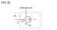
- FIG. 1B is a circuit diagram illustrating a first example of the connection position of the current control section shown in FIG. 1B.
- FIG. 1B is a circuit diagram illustrating a second example of the connection position of the current control section shown in FIG. 1B.
- FIG. It is a block diagram which shows the modification of the power module of FIG. 1A.
- 1A is a circuit diagram illustrating a configuration example of the peak detection circuit shown in FIG. 1A.
- FIG. 5 is a timing chart for explaining a temperature estimation method using the semiconductor device according to Embodiment 1.
- FIG. 3 is a circuit diagram illustrating the configuration of a peak detection circuit according to a modification of the first embodiment.
- 7 is a timing chart for explaining a temperature estimation method using a semiconductor device according to a modification of the first embodiment.
- FIG. 3 is a circuit diagram illustrating a first configuration example of a peak detection circuit according to a second embodiment.
- 7 is a circuit diagram illustrating a second configuration example of a peak detection circuit according to a second embodiment.
- FIG. 12 is a timing chart for explaining a temperature estimation method using a semiconductor device according to a third embodiment.
- FIG. 12 is a flowchart illustrating processing for calculating thermal resistance and thermal impedance by the semiconductor device according to the fourth embodiment.
- 1 is a block diagram showing the configuration of a power conversion system to which a power conversion device equipped with a semiconductor element according to the present embodiment is applied.
- FIG. 1A is a configuration diagram showing an example of a power module 101 according to the first embodiment.
- FIG. 1B is a circuit diagram showing a configuration example of the current control section 1 of FIG. 1A. The configuration of the power module 101 will be described below with reference to FIGS. 1A and 1B.
- the power module 101 includes a power semiconductor element 10 and a semiconductor device 100 that drives and controls the power semiconductor element 10.
- the semiconductor device 100 controls switching of the power semiconductor element 10 and measures the element temperature of the power semiconductor element 10.
- the power semiconductor element 10 includes a positive terminal (drain) D, a negative terminal (source) S, and a control terminal (gate) G.
- the main current Imt flowing between the positive terminal D and the negative terminal S is controlled by the drive voltage applied to the control terminal G.
- the power semiconductor element 10 may be a MOSFET, an IGBT, a MESFET (Metal-Semiconductor Field-Effect Transistor), a bipolar transistor, or the like. In the following, explanation will be given using MOSFET as an example. Further, as the material of the power semiconductor element 10, other than Si, SiC, GaN , Ga2O3 , diamond, etc. may be used.
- the semiconductor device 100 includes a gate drive section 4, a current control section 1, a gate wiring section 2, a timing control section 3, a peak detection circuit 5, a voltage detection section 6, and a temperature estimation section 7.
- the gate drive section 4 includes a driver circuit 42 as a drive control section that is connected to the power semiconductor element 10 and drives the power semiconductor element 10, and a main control section 41 that controls the driver circuit 42.
- the control terminal G of the power semiconductor element 10 is connected to the driver circuit 42 through the resistance element 21 provided in the gate wiring section 2.
- the gate wiring section 2 represents a series of loop wiring connecting the control terminal G, the negative terminal S, and the driver circuit 42 of the power semiconductor element 10.
- the resistive element 21 is connected between the driver circuit 42 and the control terminal G of the power semiconductor element 10.
- the current control unit 1 is connected to the driver circuit 42 and supplies current to a path formed between the control terminal G and the negative terminal S of the power semiconductor element 10 via the driver circuit 42.
- the current control unit 1 includes a pulse current source 20 for supplying a pulsed current.
- the pulse current source 20 includes, for example, a current source 11 that supplies a constant current, and a current control switch 12 connected in parallel to the current source 11.
- the current control switch 12 is turned on or off according to a switch control signal 31 from the timing control section 3.
- the pulse current source 20 starts outputting current
- the pulse current source 20 starts outputting current. finish. In this way, the output current of the current control section 1 is controlled in a pulsed manner according to whether the current control switch 12 is turned on or off.
- each of the current source 11 and the current control switch 12 is connected to a reference potential node 90 that provides a reference potential.
- the reference potential is, for example, the control ground of the driver circuit 42 or the power supply voltage of the driver circuit 42.
- the other ends of the current source 11 and the current control switch 12 are directly or indirectly electrically connected to the control terminal G or the negative terminal S of the power semiconductor element 10.
- the other ends of the current source 11 and the current control switch 12 are connected to the power semiconductor element 10 via other electronic components such as semiconductor switching elements or resistors mounted on the driver circuit 42. It is connected to the control terminal G (gate) or the negative terminal S (source) of.
- FIG. 2B shows a configuration example in which the other ends of the current source 11 and the current control switch 12 are electrically connected to the control terminal G of the power semiconductor element 10.
- the current control unit 1 is indirectly connected to the control terminal G via the driver circuit 42, so that it is connected to a position where current is supplied from the control terminal G side of the power semiconductor element 10.
- the other ends of the current source 11 and the current control switch 12 are electrically connected to the negative terminal S of the power semiconductor element 10 (FIG. 2A).
- the timing control section 3 and the gate drive section 4 are clearly shown separately for explanation, but the timing control section 3 may be included in the main control section 41. Further, the driver circuit 42 and the timing control section 3 may be mounted on the same board, or the main control section 41, the driver circuit 42, the timing control section 3, and the current control section 1 may all be mounted on the same board. I don't mind if you do.
- the voltage detection section 6 detects the output voltage of the peak detection circuit 5.
- the temperature estimation section 7 calculates the estimated temperature of the power semiconductor element 10 from the output voltage value of the peak detection circuit 5 at a predetermined timing based on the detection value of the voltage detection section 6 and the control information 32 of the timing control section 3. calculate. For example, as explained below, the temperature estimator 7 calculates the resistance value of the power semiconductor element 10 from the output voltage value. Furthermore, the temperature estimating unit 7 calculates the newly measured power semiconductor element 10 by comparing it with conversion data indicating the relationship between the resistance value and the element temperature, which is predetermined based on the measured value in the actual experiment in advance. Temperature information 71 is generated that includes an estimated temperature obtained by converting the resistance value of .
- FIG. 3 is a configuration diagram showing a modification of the power module 101 in FIG. 1A.
- the resistance element 21 in the gate wiring section 2, is connected not to the wiring connected to the control terminal G (gate wiring) but to the wiring connected to the negative terminal S (source wiring). It differs from the power module 101 in FIG. 1A in that it is connected. In this case as well, the resistance element 21 still causes a voltage drop in the gate wiring portion 2 in accordance with the current flowing between the control terminal G and the negative terminal S. Since the other points in FIG. 3 are the same as those in FIG. 1A, the same or corresponding parts are given the same reference numerals and the description will not be repeated. Further, in each of FIGS. 1A and 3, the resistance element 21 is clearly shown outside the power semiconductor element 10, but depending on the application, there may be cases where no gate resistance is provided outside the power semiconductor element 10.
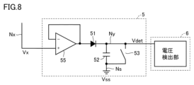
- the discharge switch 53 is connected in parallel with the capacitor 52 and turned on and off according to the switch control signal 35 from the timing control section 3.
- the discharge switch 53 can be configured by, for example, a MOSFET with a small leakage current in order to maintain the potential of the node Ny in an off state.
- the waveforms up to time t2 are the voltage and signal waveforms during normal switching operation without temperature measurement
- the waveforms after time t2 are the voltage and signal waveforms when temperature measurement is performed along with the switching operation. show. First, the operation of the semiconductor device 100 during normal switching operation will be described.
- the driver circuit 42 outputs a positive potential Vcc higher than the threshold voltage and a potential Vee lower than the threshold voltage (usually a negative potential or zero potential) to drive the power semiconductor element 10.
- the driver circuit 42 applies a positive potential Vcc or a negative or zero potential Vee as a gate voltage to the control terminal G of the power semiconductor element 10 based on the driver input signal 411 from the main control unit 41. Thereby, the driver circuit 42 causes the power semiconductor element 10 to transition between the on state and the off state.
- the timing control section 3 controls the current control switch 12 of the current control section 1 to always be in the on state. Therefore, when an enhancement type element such as an n-type MOSFET is used in the current control switch 12, a logic high (H) level signal is always input as the switch control signal 31 of the current control switch 12. If a depletion type element such as a p-type MOSFET is used in the current control switch 12, a logic low (L) level signal is always input as the switch control signal 31.
- the driver input signal 411 changes from H level to L level at time t1.
- a negative or zero potential Vee is applied to the control terminal G of the power semiconductor element 10, and the gate voltage Vgs decreases.
- the gate voltage Vgs reaches a negative or zero potential Vee at time t1x after a falling period as in the case of turn-on.
- the gate current flows through the current control switch 12 to the reference potential node 90.
- the current from current source 11 flows to reference potential node 90 via current control switch 12 and is not output to driver circuit 42 . Note that a mirror period is also observed during the falling period from time t1 to t1x.
- the period in which the gate voltage is stable includes a period in which the gate voltage is stable at a positive potential Vcc (hereinafter referred to as an "on period") and a period in which the gate voltage is stable at a negative or zero potential Vee ( (hereinafter referred to as the "off period").
- this delay time is short, the gate drive current from the driver circuit 42 will also affect the detection voltage of the voltage detection section 6, which will affect the accuracy of temperature measurement.
- this delay time is long, the time t4 at which the switch control signal 31 is returned to the H level becomes closer to the turn-off start time t5.
- the gate drive current from the driver circuit 42 also affects the voltage detected by the voltage detection section 6, thereby affecting the accuracy of temperature measurement.
- Vx (t ⁇ t3) represents the input voltage of the peak detection circuit 5 at time t after time t3.
- R gint is the value of the gate resistance (built-in gate resistance) present in the power semiconductor element 10.
- the built-in gate resistor is made of a material such as polysilicon on the power semiconductor element 10, for example.
- the built-in gate resistance includes a parasitic resistance due to the gate wiring pattern on the power semiconductor element 10.
- Rg in equation (1) represents the value of the resistance on the driver circuit 42 and the resistance element 21, and represents a resistance component other than the resistance caused by the power semiconductor element 10 itself.
- R g is provided by a resistor externally attached to the power semiconductor element 10, so selection of the resistance value and temperature characteristics is relatively easy.
- C die represents the capacitance value seen from the gate side (in the case of FIG. 2A) or the source side (in the case of FIG. 2B) of the power semiconductor element 10.
- Ig represents the supply current from the current source 11.
- the input voltage Vx becomes (t -t3) ⁇ I g /C die .
- the parasitic capacitance C die is constant and the current I g of the current source 11 is a constant value
- the input voltage Vx of the peak detection circuit 5 increases linearly.
- the resistance value (R g +R gint ) is calculated using the voltage value V1 of the detected voltage Vdet at time t4, the time difference between times t3 and t4, and the known I g corresponding to the output current of the current source 11. can do.
- each of the resistance values R g and R gint has temperature dependence. If each of the resistance values R g and R gint has a linear temperature dependence, the resistance values R g (T) and R gint at temperature T can be calculated using the temperature coefficient K, and the resistance values R g (T) ⁇ R It is expressed as g 0 ⁇ (1+K 1 ⁇ T) and R gint (T) ⁇ Rg int 0 ⁇ (1+K 2 ⁇ T).
- the temperature dependence of the resistance value R g of the power semiconductor element 10 other than the built-in gate resistance is sufficiently smaller than the temperature dependence of the built-in gate resistance value R gint of the power semiconductor element 10 , that is, the resistance value caused by the temperature T is Regarding the difference, if ⁇ R g ⁇ R gint (K 1 ⁇ K 2 ), the temperature dependence of the resistance value (R g +R gint ) represents the temperature dependence of the built-in gate resistance of the power semiconductor element 10. .
- a resistance element for example, resistance element 21
- the estimated temperature of the power semiconductor element 10 is calculated by comparing the resistance value (R g +R gint ) obtained by the above calculation with calibration data representing the relationship between the resistance value and temperature recorded in advance.
- calibration data can be used, for example, when the power module 101 is installed in a constant temperature oven and the element temperature of the power semiconductor element 10 is changed from the outside, and the resistance value (R g +R gint ) is calculated using the same method as above. It can be obtained by asking for .
- the rate of change in the built-in gate resistance value R gint due to temperature may be obtained in advance as information indicating the relationship between the temperature and the resistance value of the power semiconductor element 10.
- the temperature of the power semiconductor element 10 may be calculated by calculation using the calculated resistance value (R g +R gint ) and the temperature coefficient K 2 (K 2 >K 1 ) obtained in advance. be.
- the detection voltage Vdet is as follows.
- the resistance value (R g +R gint ) is included as a variable. Therefore, the temperature and resistance of the power semiconductor element 10 are calculated so that the estimated temperature is directly calculated from the detected voltage Vdet or V0 extracted from the detected voltage Vdet without going through the calculation of the resistance value (R g +R gint ). It is also possible to set information indicating the relationship with the value in advance.
- the current control switch 12 of the current control unit 1 (FIG. 1B etc.) is turned off.
- the current from current source 11 flows not to reference potential node 90 but to power semiconductor element 10 . That is, the current control unit 1 supplies current between the control terminal G and the negative terminal S, and the current supply period is provided during the off period.
- the voltage value V2 of the detection voltage Vdet from time t7 to t7x, the time difference (length of the current supply period) from time t6 to t7, and the current source 11 Using a known I g corresponding to the output current of , the resistance value (R g +R gint ) can be calculated.
- the output current (I g ) of the current source 11 and the time difference between times t6 and t7 (the length of the current supply period by the current control unit 1) are each maintained constant. Under these conditions, it is also possible to directly calculate the estimated temperature from the detected voltage Vdet or V0 extracted from the detected voltage Vdet, without calculating the resistance value (R g +R gint ).
- the timing at which the switch control signal 31 transitions from the H level to the L level (timing to start supplying current from the current source 11) and the timing at which the switch control signal 35 transitions from the H level to the L level ( (corresponding to the start timing of voltage detection), but it is also possible to set a certain time difference between the two.
- the current Ig from the current source 11 is injected into the path between the control terminal G and the negative terminal S during the on period or the off period of the power semiconductor element 10.
- the temperature of the power semiconductor element 10 can be stably estimated.
- the timing to start injection of the above current is determined from the rise and fall timing of the driver voltage, simply after the elapse of a time constant determined by the gate resistance and element capacitance, or a delay time set as a longer time. Can be done.
- FIG. 6 is a circuit diagram illustrating the configuration of the peak detection circuit 5 according to a modification of the first embodiment.
- peak detection circuit 5 has the configuration shown in FIG. 6 in semiconductor device 100 of FIG. 1A.
- the discharge switch 53 in the circuit configuration of FIG. 4 is replaced with a resistive element 54. That is, in the modification of the first embodiment, on/off control of the discharge switch 53 is not necessary, and the configuration of the peak detection circuit 5 is simplified.
- FIG. 7 is a timing chart for explaining a temperature estimation method using a semiconductor device according to a modification of the first embodiment.
- the capacitor 52 is discharged via the resistance element 54 from time t4 in the on period and time t7 in the off period when the current control switch 12 of the current control unit 1 is turned off in response to the switch control signal 31. Ru.
- the detection voltage Vdet gradually decreases according to the RC time constant determined by the capacitance value of the capacitor 52 and the resistance value of the resistive element 54.
- the sampling timing of the voltage value for calculating the resistance value is set to the detection voltage Vdet shown in FIG. Fix the time so that it remains constant.
- the power semiconductor element 10 temperature can be determined stably.
- Embodiment 2 In the second embodiment, a further modification of the configuration of the peak detection circuit 5 will be described.
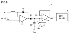
- FIG. 8 is a circuit diagram illustrating a first configuration example of the peak detection circuit according to the second embodiment.
- the peak detection circuit 5 according to the first configuration example of the second embodiment further includes an operational amplifier 55 in addition to the configuration shown in FIG. Operational amplifier 55 is connected between input node Nx and diode 51 (anode).
- a part of the current from the current control section 1, that is, a part of the supply current (I g ) of the current source 11 is transmitted between the input node Nx and the node Ns that are connected in parallel with the current source 11. It flows into the capacitor 52 and is used to charge the capacitor 52. Therefore, when the temperature is estimated from the relationship in equation (1) above, there is a possibility that the accuracy of temperature estimation may be reduced due to an error corresponding to the current flowing through the peak detection circuit 5.
- the error in the temperature calculated according to the relationship of equation (1) is reduced, and the temperature estimation accuracy of the power semiconductor element 10 is improved. can be improved.
- the operational amplifier 58 is connected between the node Ny and the voltage detection section 6.
- the operational amplifier 58 is connected as a voltage follower and outputs a voltage equivalent to the voltage of the node Ny to the voltage detection section 6 as a detection voltage Vdet.
- the arrangement of the operational amplifier 58 reduces the output impedance of the peak detection circuit 5. As a result, it is expected that the voltage detection accuracy in the voltage detection section 6 will be improved. Further, since it is possible to prevent the potential of the node Ny from changing due to the influence from the voltage detection section 6, the detection accuracy of the detection voltage Vdet can be improved from this point of view as well.
- the operational amplifier 58 can be additionally connected between the node Ny and the voltage detection section 6 also in the first configuration example shown in FIG.
- the operational amplifier 58 also corresponds to an example of an "impedance conversion circuit.”
- Embodiment 3 a modification of the on/off control of the current control switch 12 of the current control section 1 will be described.
- the off-period of the current control switch 12 is set once during each of the on-period and off-period as a period in which the gate voltage of the power semiconductor element 10 is stable other than the rising and falling periods.
- the off period of the current control switch 12 is provided multiple times.
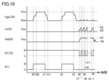
- FIG. 10 is a timing chart for explaining a temperature estimation method using a semiconductor device according to the third embodiment.
- the off-period of the current control switch 12 that is, the period of current supply from the current source 11, is provided multiple times.
- temperature measurement is performed during the off period after time t5 when the power semiconductor element 10 is turned off.
- the switch control signal 31 is set to the L level from time t6 to time t7, which is after a certain delay period has elapsed from time t5, which corresponds to the turn-off command timing.
- a current supply period from the current control section 1 is provided. As described in Embodiment 1, in this period, current is supplied from the current source 11 to the power semiconductor element 10 via the gate wiring section 2, so that the peak detection circuit 5 The input voltage Vx of increases.
- the switch control signal 31 changes from L level to H level.
- an L level period of the switch control signal 31 is provided again between times t8 and t9. Furthermore, after the switch control signal 31 changes from the L level to the H level at time t9, an L level period of the switch control signal 31 is provided again between times t10 and t11.
- the switch control signal 31 goes to the L level multiple times from time t6 to t7, time t8 to t9, time t10 to t11, ..., time tk-1 to tk.
- a period that is, a period in which current is supplied from the current control section 1 by turning off the current control switch 12 is provided.
- the lengths of the L level periods of the switch control signal 31 are set to be equal. Therefore, the behavior (waveform) of the input voltage Vx is the same in each L level period of the switch control signal 31. Therefore, the input voltage Vx at the end of each L level period of the switch control signal 31 has the same voltage value V2.
- the current control switch 12 by turning the current control switch 12 on and off a plurality of times and providing a current supply period multiple times, the output voltage of the peak detection circuit 5, that is, the detection of the voltage detection section 6 Attenuation of the voltage Vdet can be canceled out.
- a simple detector with a slow time response speed can be used as the voltage detection section 6. Note that the on/off operation of the current control switch 12 is repeated throughout the period when the gate voltage of the power semiconductor element 10 is stable other than the rising period and the falling period, that is, the OFF period and the ON period. Can be done.
- the off-period length of the current control switch 12 may not take exactly the same value due to the influence of controller jitter, etc. If the off-period length varies, the peak value of the input voltage Vx will include a change factor other than the temperature of the power semiconductor element 10, so there is a concern that the temperature estimation accuracy will deteriorate. Even in such a case, as in the third embodiment, by providing an off period for the current control switch 12, that is, a measurement period for the input voltage Vx, within one off period or on period, errors due to jitter can be reduced. The effects can be averaged out. Thereby, it is possible to avoid a decrease in temperature estimation accuracy.
- Embodiment 4 In Embodiment 4, an example will be described in which the steady thermal resistance or transient thermal resistance of power semiconductor element 10 is calculated using the estimated temperature calculation value of power semiconductor element 10 calculated in Embodiments 1 to 3.
- the power semiconductor element 10 When calculating the steady-state thermal resistance, the power semiconductor element 10 needs to be in a thermally steady state (thermal equilibrium state).
- the steady state is, for example, a state in which a certain amount of power loss is generated by passing a certain amount of direct current through the power semiconductor device 10, as in a power cycle test, which is one of the general reliability tests for power semiconductor devices. It can be realized with.
- a pseudo thermal equilibrium state can be created by continuously switching the power semiconductor element 10 and controlling the current flowing through the power semiconductor element 10 to a constant amount.
- a full-bridge circuit that uses four power semiconductor devices to control the direction of current conduction, or a half-bridge circuit that uses two power semiconductor devices with a thick inductive load or a resistive load.
- a pseudo thermal equilibrium state can be created by controlling the current of each power semiconductor element to a constant amount.
- FIG. 11 is a configuration diagram showing an example of a power module according to the fourth embodiment.
- power module 103 according to Embodiment 4 has a main power module for measuring main current Imt. It further includes a current detection section 81 and a main voltage detection section 82 for detecting the main voltage (drain-source voltage) Vmt of the power semiconductor element 10 .
- the main current Imt measured by the main current detection section 81 and the main voltage Vmt detected by the main voltage detection section 82 are input to the main control section 41 .
- the main control unit 41 can calculate the power loss occurring in the power semiconductor element 10 by the product of the main voltage Vmt and the main current Imt.
- power semiconductor element 10 is subjected to switching control multiple times to form the above-mentioned thermal equilibrium state until time t5, and then is maintained in the off state after time t5.
- Embodiment 4 the temperature change of power semiconductor element 10 maintained in an off state for a long period of time is measured by the method described in Embodiment 3, thereby determining the thermal resistance and heat of power semiconductor element 10. Measure impedance.
- the peak detection circuit 5 Since the power semiconductor element 10 is maintained in the off state after time t5, it is gradually cooled down. Therefore, the peak value of the input voltage Vx and the detection voltage Vdet gradually decrease depending on the temperature element of the power semiconductor element 10. In order to calculate the decrease in temperature Tj by decreasing the detection voltage Vdet, the peak detection circuit 5 needs to have a response speed that can reflect the decrease in the peak value of the input voltage Vx due to the decrease in the temperature of the power semiconductor element 10 on the detection voltage Vdet. There is. For this reason, the response time constant of the peak detection circuit 5 is preferably shorter than the thermal time constant of the power semiconductor element 10.
- FIG. 13 is a flowchart illustrating processing for calculating thermal resistance and thermal impedance by the semiconductor device according to the fourth embodiment.
- the series of processes shown in FIG. 13 is executed by the main control unit 41, for example.
- the main control unit 41 acquires the main voltage Vmt (instantaneous value) of the power semiconductor element 10 measured by the main voltage detection unit 82, and in S120, the main control unit 41 obtains the main voltage Vmt (instantaneous value) of the power semiconductor element 10 measured by the main current detection unit 81. Obtain the main current Imt (instantaneous value). Since the main voltage Vmt acquired in S110 and the main current Imt acquired in S120 are measured values at the same timing, the main control unit 41 calculates the multiplication value of the main voltage Vmt and the main current Imt in S130. From this, the power loss Pls (instantaneous value) generated in the power semiconductor element 10 is calculated.
- the main control unit 41 makes a NO determination in S140 until the thermal resistance calculation timing arrives.
- the main control unit 41 determines NO in S140
- the main control unit 41 executes a process of calculating the power loss Plsc of the power semiconductor element 10 for each switching cycle in S150.
- the power loss Pls for each switching cycle is calculated by integrating the power losses Pls calculated in S130 within each switching cycle.
- the integrated value is cleared in response to the end or start of each switching cycle.
- S140 is determined to be YES at time t5.
- the processes of S110 to S150 are repeatedly executed until a YES determination is made in S140.
- a moving average value of the power loss Plsc for the latest X cycles (X: a predetermined integer of 2 or more) may be further calculated.
- the main control unit 41 When the main control unit 41 makes a YES determination in S140, it advances the process to S160 and starts calculating the thermal resistance. In S160, the main control unit 41 determines the power P (W) used for calculating the thermal resistance Rth.
- the power P can be the power loss Plsc in the immediately previous switching cycle calculated in S150 at the time when S140 is determined to be YES, or the latest moving average value of the power losses Plsc.
- the main controller 41 calculates the estimated temperature of the power semiconductor element 10 from the detected voltage Vdet obtained as the peak value of the input voltage Vx every L level period (equal length) of the switch control signal 31. (estimated value of Tj) is calculated.
- Tj the estimated value of Tj
- the main control unit 41 calculates the thermal resistance (here, Rth(2) ⁇ Rth(N)), the thermal impedance Zth of the power semiconductor element 10 including the cooling system can be calculated.
- the thermal resistance calculation section can be configured by the main control section 41 executing the control process shown in FIG. 13.
- cooling time depends on the thermal time constant of the cooling system of the power semiconductor element 10, but is generally on the order of several [s] to several hundred [s]. Cooling times of this order are difficult to incorporate into the normal operating mode of typical power electronic equipment, but for example, in inverter systems, current control can be used to keep power semiconductor devices off for a certain period of time, or By utilizing the system operation stop timing, it is possible to maintain the off state of the power semiconductor element 10 for a relatively long period of time and perform the thermal impedance calculation process shown in FIG. 13.
- Embodiment 5 the power modules 101 to 103 according to the first to fourth embodiments described above are applied to a power conversion device.
- the present disclosure is not limited to a specific power conversion device, a case will be described below as Embodiment 5 in which the present disclosure is applied to a three-phase inverter.
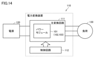
- FIG. 14 is a block diagram showing the configuration of a power conversion system to which the power conversion device according to the present embodiment is applied.
- the power conversion system shown in FIG. 14 includes a power source 120, a power conversion device 110, and a load 130.
- Power supply 120 is a DC power supply and supplies DC power to power conversion device 110.
- the power source 120 can be composed of various things, for example, it can be composed of a DC system, a solar battery, a storage battery, or it can be composed of a rectifier circuit or an AC/DC converter connected to an AC system. Good too. Further, the power supply 120 may be configured by a DC/DC converter that converts DC power output from a DC system into set power.
- the load 130 is a three-phase electric motor driven by AC power supplied from the power converter 110.
- the load 130 is not limited to a specific application, but is a motor installed in various electrical devices, and is used, for example, as a motor for a hybrid vehicle, an electric vehicle, a railway vehicle, an elevator, or an air conditioner.
- the main conversion circuit 111 includes a switching element and a freewheeling diode (not shown), and when the switching element switches, it converts the DC power supplied from the power supply 120 into AC power, and supplies the AC power to the load 130.
- the main conversion circuit 111 is a two-level three-phase full bridge circuit, and has six switching elements and each switching element. It can be constructed from six freewheeling diodes arranged in antiparallel. At least one of the switching elements of the main conversion circuit 111 is the power semiconductor element 10 included in the power module 101 of any one of the first to fourth embodiments described above.
- the six switching elements are connected in series every two switching elements to constitute upper and lower arms, and each upper and lower arm constitutes each phase (U phase, V phase, W phase) of the full bridge circuit.
- the output terminals of the upper and lower arms that is, the three output terminals of the main conversion circuit 111, are connected to the load 130.
- the main conversion circuit 111 is a semiconductor device. It is equipped with 100.
- the semiconductor device 100 generates a drive signal for driving the switching element of the main conversion circuit 111 and supplies it to the control electrode of the switching element of the main conversion circuit 111.
- a drive signal that turns the switching element on and a drive signal that turns the switching element off are output to the control electrode of each switching element.
- the drive signal When keeping the switching element in the on state, the drive signal is a voltage signal (on signal) that is greater than or equal to the threshold voltage of the switching element, and when the switching element is kept in the off state, the drive signal is a voltage signal that is less than or equal to the threshold voltage of the switching element. signal (off signal).
- the control circuit 112 controls the switching elements of the main conversion circuit 111 so that the desired power is supplied to the load 130. Specifically, the time (on time) during which each switching element of the main conversion circuit 111 should be in the on state is calculated based on the power to be supplied to the load 130.
- the main conversion circuit 111 can be controlled by PWM (Pulse Width Modulation) control that modulates the on-time of the switching element according to the voltage to be output. Then, a control command (control signal ) is output.
- the semiconductor device 100 outputs an on signal or an off signal as a drive signal to the control electrode of each switching element.
- the power modules 101 to 103 according to the first to fourth embodiments are applied as the power module 101 constituting the main conversion circuit 111, the The reliability of the power conversion device can be improved.
- the present disclosure is not limited to this and can be applied to various power conversion devices.
- a two-level power converter is used, but a three-level or multi-level power converter may also be used, and when supplying power to a single-phase load, the present disclosure may be applied to a single-phase inverter. May be applied.
- the present disclosure can also be applied to a DC/DC converter or an AC/DC converter.
Landscapes
- Engineering & Computer Science (AREA)
- Power Engineering (AREA)
- Power Conversion In General (AREA)
- Electronic Switches (AREA)
Abstract
Dans un dispositif à semi-conducteur (100) pour commander l'attaque d'un élément semi-conducteur (10), une unité de commande de courant (1) est prévue pour faire passer un courant pulsé entre une borne d'électrode négative (S) et une borne de commande (G) de l'élément semi-conducteur (10). Un circuit de détection de crête (5) détecte une valeur crête d'une tension entre la borne de commande (G) ou la borne d'électrode négative (S) et un potentiel de référence pendant la période d'une alimentation en courant par l'unité de commande de courant (1). Une unité d'estimation de température (7) calcule une température estimée de l'élément semi-conducteur sur la base d'une tension de sortie du circuit de détection de crête (5) prélevée par une unité de détection de tension (6). Une unité de commande de minutage (3) amène l'unité de commande de courant (1) à fonctionner de façon à assurer la période d'alimentation en courant dans une période passante après que l'élément semi-conducteur a transité vers un état passant et/ou dans une période bloquée après que l'élément semi-conducteur a transité vers un état bloqué.
Priority Applications (1)
| Application Number | Priority Date | Filing Date | Title |
|---|---|---|---|
| PCT/JP2022/024679 WO2023248335A1 (fr) | 2022-06-21 | 2022-06-21 | Dispositif à semi-conducteur et dispositif de conversion d'énergie électrique |
Applications Claiming Priority (1)
| Application Number | Priority Date | Filing Date | Title |
|---|---|---|---|
| PCT/JP2022/024679 WO2023248335A1 (fr) | 2022-06-21 | 2022-06-21 | Dispositif à semi-conducteur et dispositif de conversion d'énergie électrique |
Publications (1)
| Publication Number | Publication Date |
|---|---|
| WO2023248335A1 true WO2023248335A1 (fr) | 2023-12-28 |
Family
ID=89379499
Family Applications (1)
| Application Number | Title | Priority Date | Filing Date |
|---|---|---|---|
| PCT/JP2022/024679 WO2023248335A1 (fr) | 2022-06-21 | 2022-06-21 | Dispositif à semi-conducteur et dispositif de conversion d'énergie électrique |
Country Status (1)
| Country | Link |
|---|---|
| WO (1) | WO2023248335A1 (fr) |
Citations (5)
| Publication number | Priority date | Publication date | Assignee | Title |
|---|---|---|---|---|
| JP2013142704A (ja) * | 2012-01-11 | 2013-07-22 | Abb Research Ltd | Igbtデバイスの動作状態を実時間で監視するシステムと方法 |
| JP2014241672A (ja) * | 2013-06-11 | 2014-12-25 | サンケン電気株式会社 | 半導体装置及びその制御方法 |
| JP2019519182A (ja) * | 2016-04-28 | 2019-07-04 | マシイネンフアブリーク・ラインハウゼン・ゲゼルシヤフト・ミツト・ベシユレンクテル・ハフツング | 結合部の温度と電流の検知 |
| JP2019122107A (ja) * | 2017-12-28 | 2019-07-22 | ルネサスエレクトロニクス株式会社 | 電力変換装置および半導体装置 |
| JP7042991B1 (ja) * | 2021-06-29 | 2022-03-28 | 三菱電機株式会社 | 半導体装置および電力変換装置 |
-
2022
- 2022-06-21 WO PCT/JP2022/024679 patent/WO2023248335A1/fr unknown
Patent Citations (5)
| Publication number | Priority date | Publication date | Assignee | Title |
|---|---|---|---|---|
| JP2013142704A (ja) * | 2012-01-11 | 2013-07-22 | Abb Research Ltd | Igbtデバイスの動作状態を実時間で監視するシステムと方法 |
| JP2014241672A (ja) * | 2013-06-11 | 2014-12-25 | サンケン電気株式会社 | 半導体装置及びその制御方法 |
| JP2019519182A (ja) * | 2016-04-28 | 2019-07-04 | マシイネンフアブリーク・ラインハウゼン・ゲゼルシヤフト・ミツト・ベシユレンクテル・ハフツング | 結合部の温度と電流の検知 |
| JP2019122107A (ja) * | 2017-12-28 | 2019-07-22 | ルネサスエレクトロニクス株式会社 | 電力変換装置および半導体装置 |
| JP7042991B1 (ja) * | 2021-06-29 | 2022-03-28 | 三菱電機株式会社 | 半導体装置および電力変換装置 |
Similar Documents
| Publication | Publication Date | Title |
|---|---|---|
| KR102294347B1 (ko) | 정션 온도 및 전류 감지 기법 | |
| Rothmund et al. | Accurate transient calorimetric measurement of soft-switching losses of 10-kV SiC MOSFETs and diodes | |
| US9935577B2 (en) | Semiconductor device and fault detecting method | |
| US11709186B2 (en) | Methods and circuitry for analyzing voltages | |
| Chen et al. | On-line monitoring of the MOSFET device junction temperature by computation of the threshold voltage | |
| Rothmund et al. | Accurate transient calorimetric measurement of soft-switching losses of 10kV SiC MOSFETs | |
| US10153696B2 (en) | Methods and circuitry for sampling a signal | |
| US10263615B2 (en) | Circuit and method for driving a device through drive cycles | |
| Koenig et al. | On-line junction temperature measurement of CoolMOS devices | |
| Zhang et al. | Online junction temperature monitoring using turn-off delay time for silicon carbide power devices | |
| Yang et al. | A method of junction temperature estimation for SiC power MOSFETs via turn-on saturation current measurement | |
| Yang et al. | A method for junction temperature estimation utilizing turn-on saturation current for SiC MOSFET | |
| JP2010206699A (ja) | ソレノイド電流制御回路 | |
| Anurag et al. | An accurate calorimetric method for measurement of switching losses in silicon carbide (SiC) MOSFETs | |
| Li et al. | Experimental investigation of GaN transistor current collapse on power converter efficiency for electrical vehicles | |
| US11923785B2 (en) | Power module for the operation of an electric vehicle drive with improved temperature determination of the power semiconductor | |
| Chen et al. | Driver Integrated Online R ds-on Monitoring Method for SiC Power Converters | |
| Pai et al. | A new behavioral model for accurate loss calculations in power semiconductors | |
| US11728748B2 (en) | Power module for operating an electric vehicle drive with improved temperature determination of the power semiconductors | |
| WO2023275981A1 (fr) | Dispositif à semi-conducteurs et dispositif de conversion de puissance | |
| WO2023248335A1 (fr) | Dispositif à semi-conducteur et dispositif de conversion d'énergie électrique | |
| EP3419171A1 (fr) | Procédé et appareil de surveillance d'un commutateur semi-conducteur | |
| KR101531018B1 (ko) | 전력반도체소자의 불량 예측 방법 | |
| Górecki | Investigation of the influence of thermal phenomena on characteristics of IGBTs contained in power modules | |
| US11955771B2 (en) | Control device and method for laser device and laser measurement device |
Legal Events
| Date | Code | Title | Description |
|---|---|---|---|
| 121 | Ep: the epo has been informed by wipo that ep was designated in this application |
Ref document number: 22947898 Country of ref document: EP Kind code of ref document: A1 |