WO2023248271A1 - 電界放出電子源とその製造方法およびそれを用いた電子線装置 - Google Patents
電界放出電子源とその製造方法およびそれを用いた電子線装置 Download PDFInfo
- Publication number
- WO2023248271A1 WO2023248271A1 PCT/JP2022/024469 JP2022024469W WO2023248271A1 WO 2023248271 A1 WO2023248271 A1 WO 2023248271A1 JP 2022024469 W JP2022024469 W JP 2022024469W WO 2023248271 A1 WO2023248271 A1 WO 2023248271A1
- Authority
- WO
- WIPO (PCT)
- Prior art keywords
- plane
- electron source
- single crystal
- field emission
- tip
- Prior art date
- Legal status (The legal status is an assumption and is not a legal conclusion. Google has not performed a legal analysis and makes no representation as to the accuracy of the status listed.)
- Ceased
Links
Images











Classifications
-
- H—ELECTRICITY
- H01—ELECTRIC ELEMENTS
- H01J—ELECTRIC DISCHARGE TUBES OR DISCHARGE LAMPS
- H01J37/00—Discharge tubes with provision for introducing objects or material to be exposed to the discharge, e.g. for the purpose of examination or processing thereof
- H01J37/02—Details
- H01J37/04—Arrangements of electrodes and associated parts for generating or controlling the discharge, e.g. electron-optical arrangement or ion-optical arrangement
- H01J37/06—Electron sources; Electron guns
- H01J37/073—Electron guns using field emission, photo emission, or secondary emission electron sources
-
- H—ELECTRICITY
- H01—ELECTRIC ELEMENTS
- H01J—ELECTRIC DISCHARGE TUBES OR DISCHARGE LAMPS
- H01J1/00—Details of electrodes, of magnetic control means, of screens, or of the mounting or spacing thereof, common to two or more basic types of discharge tubes or lamps
- H01J1/02—Main electrodes
- H01J1/30—Cold cathodes, e.g. field-emissive cathode
- H01J1/304—Field-emissive cathodes
-
- H—ELECTRICITY
- H01—ELECTRIC ELEMENTS
- H01J—ELECTRIC DISCHARGE TUBES OR DISCHARGE LAMPS
- H01J9/00—Apparatus or processes specially adapted for the manufacture, installation, removal, maintenance of electric discharge tubes, discharge lamps, or parts thereof; Recovery of material from discharge tubes or lamps
- H01J9/02—Manufacture of electrodes or electrode systems
-
- H—ELECTRICITY
- H01—ELECTRIC ELEMENTS
- H01J—ELECTRIC DISCHARGE TUBES OR DISCHARGE LAMPS
- H01J9/00—Apparatus or processes specially adapted for the manufacture, installation, removal, maintenance of electric discharge tubes, discharge lamps, or parts thereof; Recovery of material from discharge tubes or lamps
- H01J9/02—Manufacture of electrodes or electrode systems
- H01J9/022—Manufacture of electrodes or electrode systems of cold cathodes
- H01J9/025—Manufacture of electrodes or electrode systems of cold cathodes of field emission cathodes
-
- H—ELECTRICITY
- H01—ELECTRIC ELEMENTS
- H01J—ELECTRIC DISCHARGE TUBES OR DISCHARGE LAMPS
- H01J2237/00—Discharge tubes exposing object to beam, e.g. for analysis treatment, etching, imaging
- H01J2237/06—Sources
- H01J2237/063—Electron sources
- H01J2237/06308—Thermionic sources
- H01J2237/06316—Schottky emission
Definitions
- the present invention relates to a field emission electron source for an electron beam device such as an electron microscope, a method for manufacturing the same, and an electron beam device using the same.
- Electron microscopes have a spatial resolution that exceeds the optical limit and can observe fine structures on the order of nm to pm and analyze compositions. For this reason, it is widely used in engineering fields such as materials, physics, medicine, biology, electricity, and mechanics.
- the scanning electron microscope (SEM) is a device that can easily observe the surface of a sample.
- Electron sources used in electron beam devices such as scanning electron microscopes include thermionic emitters (TE), field emitters (FE), and Schottky emitters (SE). be.
- thermionic emitters TE
- field emitters FE
- SE Schottky emitters
- field emission electron sources FE
- FE field emission electron sources
- a W tip which uses a tungsten ⁇ 310 ⁇ crystal plane with a sharpened needle-like electrode (tip), is widely used in this field emission electron source.
- FIG. 1 shows an energy diagram representing the emission principle of a field emission electron source.
- a high electric field is applied, and the electrons e in the W tip are effectively quantum-mechanically transmitted through the thinned energy barrier and emitted into the vacuum. Since it can operate at room temperature, the energy full width at half maximum ⁇ E FE of the extracted electrons e is narrow at around 0.3 eV. In addition, it emits high-density electron beams from the narrow electron-emitting surface of the very sharp tip, so it has a high brightness of 10 8 (A/cm 2 sr).
- Field emission electron sources using hexaboride nanowires such as LaB6 which has a lower work function ⁇ than W, have been proposed in order to further narrow the full width at half maximum ⁇ E and increase the brightness B of field emission electron sources (e.g. , Patent Document 1). Since it has a lower work function barrier than W, it is possible to transmit electrons and emit field emission in a lower electric field, further reducing the energy full width at half maximum ⁇ E FE .
- the inventors used hexaboride single crystals such as CeB 6 , which had been produced by the floating zone method, to shape the tip into a hemispherical shape using electrolytic polishing, electric field evaporation, etc.
- a cold field emitter CFE
- This hexaboride single-crystal field emission electron source has better monochromaticity than the conventional W field emission electron source, and also has a low ratio of radiation angular current density J ⁇ ( ⁇ A/sr) to total current It ( ⁇ A).
- the radiation angular current density J ⁇ ( ⁇ A/sr) can be increased.
- This invention makes it possible to improve the chromatic aberration of a scanning electron microscope, especially at low accelerating voltages, and to achieve high spatial resolution in the observation of the extreme surface of a sample and the observation of light element substances such as carbon-based compounds.
- the size of hexaboride single crystals created by floating zone method etc. is about 0.1 mm to several mm, so it can be assembled into an electron source by hand or by machine, and it can be assembled into an electron source with a diameter of several tens of mm. It has the advantage that it can be produced more easily and at a higher yield at a lower cost than an electron source using nanowires with a diameter of several hundred nanometers.
- the inventors formed a facet of the (100) plane at the top of the tip of the hexaboride single crystal with the ⁇ 100> axis of the hexaboride single crystal, and probed the field emission electrons from the (100) plane.
- the results showed that the stability of the emitted current was higher than that of field emission electrons from the ⁇ 310 ⁇ plane.
- the (100) plane has a slightly higher work function than the ⁇ 310 ⁇ plane and is less susceptible to work function fluctuations due to adsorbed gas, and also has a higher atomic surface density than the ⁇ 310 ⁇ plane.
- the structure is stable and atomic vibrations are suppressed, and heating facilitates the formation of flat, large-area facets, which reduces electric field concentration, and local work due to gas adsorption and desorption during field electron emission. This is because function changes are averaged over large facets, reducing overall fluctuations. Therefore, current stability can be improved by forming a (100) facet at the tip of a ⁇ 100>-axis hexaboride single crystal tip and probing it with an electron beam emitted from the (100) plane.
- the high work function and low electric field concentration indicate that the (100) plane is less likely to emit electrons than the ⁇ 310 ⁇ plane. Since electrons emitted from the ⁇ 310 ⁇ planes formed are wasted outside the optical axis of the electron microscope, the ratio of the radiation angular current density J ⁇ ( ⁇ A/sr) to the total current It ( ⁇ A) is 1 ( The problem was that it significantly decreased to less than 1/sr).
- the electrons wastefully emitted off the optical axis will hit the extraction electrode in the electron microscope, generate electron beam-stimulated desorption gas from the electrode surface, and cause field emission electrons. It enters and adsorbs on the surface of the source, causing work function fluctuations and impairing current stability.
- Patent No. 05660564 Patent No. 06694515 International Publication No. 2022/064557
- a field emission electron source using a hexaboride single crystal such as CeB 6 has a probe with field emission electrons from the (100) plane, compared to field emission electrons from the ⁇ 310 ⁇ plane.
- the stability of the emission current is high, and the stability can be further improved by increasing the ratio J ⁇ /It of the radiation angular current density J ⁇ ( ⁇ A/sr) to the total current It ( ⁇ A).
- transition metals such as HfC, ZrC, and TiC, which are compounds with a lower work function than W and the same cubic crystal structure as hexaboride single crystals such as CeB 6 .
- the stability of the emission current is higher than that from the ⁇ 310 ⁇ plane.
- the higher the ratio J ⁇ /It of the radiation angular current density J ⁇ ( ⁇ A/sr) to the total current It ( ⁇ A) the higher the electron beam-stimulated desorption. Gas generation can be suppressed and stability is improved. Therefore, further improvements in J ⁇ /It are expected, as well as the development of new technology to suppress gas adsorption to the electron-emitting surface.
- An object of the present invention is to solve the above-mentioned problems by utilizing a stable electron beam emitted from a local region of a desired shape-wise and temporally stable electron-emitting surface that is less affected by gas adsorption; Field emission electrons from hexaboride single crystals and transition metal carbide single crystals that have both monochromaticity and long-term stability of emission current are produced using a method that suppresses the mixing of unstable electron beams emitted from other than the emission surface. It is an object of the present invention to provide an electron beam device such as an electron microscope that requires high resolution and long-term stability and can be used for various purposes.
- a field emission electron source was used which is characterized by forming microcrystals and emitting electrons from the top facet of the second (100) plane.
- single crystals containing LaB 6 or CeB 6 as main components are used as hexaboride single crystals, and single crystals containing HfC, ZrC, or TiC as main components are used as transition metal carbide single crystals, which have a low work function and are heat resistant. It is a material suitable for the present invention because it has a cubic crystal structure necessary for forming a microcrystal having a top facet of the second (100) plane at the tip tip.
- top facet of the second (100) plane is smaller than the top facet of the first (100) plane, and one side of the top facet of the first (100) plane and the top facet of the second (100) plane are smaller than the top facet of the first (100) plane.
- the ratio of one side of the facet is 0.05 to 0.35, and the microcrystal forming the top facet of the second (100) plane has a cubic shape whose side faces are also ⁇ 100 ⁇ planes, or whose side faces are ⁇ 111 ⁇ It has a trapezoidal shape formed by a group of planes, and one side of the top facet of the second (100) plane is in the range of 10 to 60 nm, and the height of the microcrystal is similar to that of the second (100) plane.
- the problem can be effectively solved by making the area 0.7 times or more larger than one side of the top facet.
- the top facet of the first (100) plane has a side of 1.5 ⁇ m or less and has a multi-stage structure of 4 or less steps, which suppresses the surface diffusion of adsorbed gas from the tip sidewall toward the electron emission surface. and can effectively solve problems.
- the tip of the rod of ⁇ 100> oriented hexaboride single crystal or transition metal carbide single crystal is electrolytically polished. is processed into a cone-shaped tip, and by applying a strong electric field that makes the tip positive polarity while heating this tip, at least 4 side facets consisting of a ⁇ n11 ⁇ surface and at least four ⁇ n10 ⁇ surfaces, and such that the total area of the side facets of ⁇ n11 ⁇ > the total area of the side facets of ⁇ n10 ⁇
- a second (100) This can be solved by forming microcrystals with a top facet.
- the present invention includes an electron source, a sample stage on which a sample is placed, and electrons emitted from the electron source are focused into a beam and irradiated onto the sample on the sample stage.
- This can be solved by providing a tip formed with a microcrystal having a top facet.
- a new field emission electron source that has both monochromaticity and long-term stability of emission current, and that this field emission electron source can be used in various applications requiring high resolution and long-term stability. It is possible to provide an electron beam device such as an electron microscope that can perform
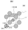
- FIG. 1 is a perspective view showing the crystal structure (unit cell) of a hexaboride single crystal used in the electron source according to Example 1.
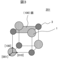
- FIG. 1 is a perspective view showing the crystal structure (unit cell) of a transition metal carbide single crystal used in the electron source according to Example 1.
- FIG. 2 is a schematic diagram showing a rectangular prism or cylindrical rod cut out along the [100] crystal axis from a hexaboride single crystal or transition metal carbide single crystal grown along the [100] crystal axis according to Example 1. .
- FIG. 1 is a perspective view showing the crystal structure (unit cell) of a hexaboride single crystal used in the electron source according to Example 1.
- FIG. 1 is a perspective view showing the crystal structure (unit cell) of a transition metal carbide single crystal used in the electron source according to Example 1.
- FIG. 2 is a schematic diagram showing a rectangular prism or cylindrical rod cut out along the [100] crystal axis from a hexaboride single crystal or transition metal
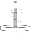
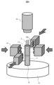
- FIG. 2 is a perspective view showing a state in which the metal tube according to Example 1 is mounted on an assembly stand with a rod of a hexaboride single crystal or a transition metal carbide single crystal. Pressure welding of a rod of a hexaboride single crystal or a transition metal carbide single crystal to a metal tube mounted on an assembly table to explain a method of joining a metal tube and a rod of a hexaboride single crystal or a transition metal carbide single crystal according to Example 1.
- FIG. 3 is a perspective view showing the positional relationship between the tool and the stereomicroscope.
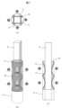
- FIG. 1 is a diagram illustrating a joining structure of a metal tube and a rectangular prism rod of a hexaboride single crystal or a transition metal carbide single crystal according to Example 1, (a) is a plan view, (b) is a perspective view, and (c) is a plan view. is a front sectional view.
- FIG. 2 is a front view of a structure serving as a prototype of an electron source, illustrating an assembly structure of an electron source according to Example 1.
- FIG. Figures illustrating the alignment jig when assembling the electron source according to Example 1, (a) is a perspective view of the alignment jig that aligns the metal tube and filament, and (b) is a perspective view of the alignment jig that aligns the filament with the spot.
- FIG. 2 is a perspective view of a welded metal tube, a stem, and an alignment jig for aligning the positions thereof.
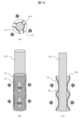
- 2 is a diagram illustrating another example of the joining structure of the metal tube and the cylindrical rod of hexaboride single crystal or transition metal carbide single crystal according to Example 1, (a) is a plan view, (b) is a perspective view, (c) is a front sectional view.
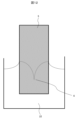
- FIG. 3 is a front sectional view showing a state in which the electron source structure is immersed in an electrolytic polishing liquid, illustrating a process of sharpening the rod tip of the electron source according to Example 1 to form a tip by electrolytic polishing.
- FIG. 2 is a front sectional view of a hexaboride tip, a transition metal carbide single crystal, and an electrolytic polishing solution, illustrating the principle of electrolytically polishing the rod tip of the electron source according to Example 1 to create a tip.
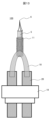
- 1 is a front view of an electron source of a hexaboride single crystal or a transition metal carbide single crystal according to Example 1.
- FIG. FIG. 3 is a diagram showing the process of forming the electron emitting surface at the tip of the tip in Examples 2 and 3; (a) is a perspective view showing the shape of the tip after electrolytic polishing; (b) is a perspective view showing the shape of the tip after electrolytic polishing; FIG.
- FIG. 7(c) is a perspective view showing the tip end shape of the tip after performing electric field treatment
- (c) is a perspective view showing the tip end shape of the tip after performing the second stage thermal electric field treatment
- 3 is a diagram showing the process condition range of the manufacturing method of Example 2
- (a) is a diagram showing the process condition range of the first stage thermal electric field treatment
- (b) is a diagram showing the process condition range of the second stage thermal electric field treatment.
- FIG. It is a figure showing a condition range. This is a cross-sectional view of the tip end showing the mechanism of formation of microcrystals having a second (100) top facet within the first (100) top facet plane in the manufacturing method of Example 2 and Example 3.
- FIG. 3 is a diagram showing the process condition range of the manufacturing method of Example 3
- (a) is a diagram showing the process condition range of the first stage thermal electric field treatment
- (b) is a diagram showing the process condition range of the second stage thermal electric field treatment.
- FIG. It is a figure showing a condition range.
- a field emission microscopic image of the tip of the transition metal carbide single crystal using HfC in Example 4 (a) is a field emission microscopic image of the field emission of the tip after the first stage heat treatment; b) is a field emission microscope image taken by field emission of the tip after the second heat treatment.
- the transition metal carbide single crystal field emission electron source using HfC in Example 4 there are cases in which only the top facet of the first (100) plane is formed and a case in which the top facet of the second (100) plane is formed. It is a graph obtained by measuring the radiation angular current density J ⁇ ( ⁇ A/sr) with respect to the total current It ( ⁇ A) when microcrystals are formed.
- Example 3 is a graph showing changes in electron emission characteristics of a field emission electron source depending on the size (length of one side) of a microcrystal having a top facet of the second (100) plane in Example 5;
- (a) is a graph showing a change in electron emission characteristics of a field emission electron source;
- (b) is a graph showing changes in radiation angular current density J ⁇ ( ⁇ A/sr), and
- (c) is a graph showing changes in light source diameter.
- Example 3 is a graph showing changes in the electron emission characteristics of the field emission electron source depending on the ratio of the height of the microcrystal to the length of one side of the top facet of the second (100) plane in Example 5, in which (a) shows the change in the electron emission characteristics of the field emission electron source; It is a graph showing the change in the electric field strength at the center, and (b) is a graph showing the change in the radiation angular current density J ⁇ ( ⁇ A/sr).
- FIG. 3 is a diagram showing changes in the electric field strength ratio with respect to the ratio of the length of one side of the top facet of the surface, (c) 1 of the top facet of the second (100) surface and the top facet of the first (100) surface;
- FIG. 3 is a diagram showing changes in radiation angular current density J ⁇ ( ⁇ A/sr) with respect to the ratio of side lengths.
- FIG. 7 is a perspective view of a tip in which the first top (100) facet of the tip of the tip of Example 6 is made in a multi-stage structure.
- FIG. 7 is a schematic cross-sectional view of an electron beam device (scanning electron microscope equipped with a field emission electron source using a hexaboride single crystal or transition metal carbide tip of the present invention) according to Example 7.
- a field emission electron source is used which is characterized in that it forms a microcrystal having a top facet of the second (100) plane and emits electrons from the top facet of the second (100) plane. The reason for this will be explained below.
- a field emission electron source using a (100) plane has higher stability of emission current than a field emission electron source using a (310) plane, but the total current
- the top (100) facet is a flat structure, and although the area is small, the ⁇ n10 ⁇ Since the surface is more pointed, the structure makes it easier for electric fields to concentrate, making it difficult to further increase J ⁇ /It.
- At least four ⁇ n11 ⁇ planes and at least four ⁇ n10 ⁇ planes are integers. forming a top facet of the first (100) plane surrounded by side facets consisting of and such that the total area of the side facets of the ⁇ n11 ⁇ planes > the total area of the side facets of ⁇ n10 ⁇ Furthermore, by forming a microcrystal having a top facet of a second (100) plane within the top facet of the first (100) plane, an electric field is applied to the top facet of the second (100) plane.
- Example 1 the structure of a field emission electron source (hereinafter sometimes simply referred to as an electron source) of the present invention and its assembly method will be explained using FIGS. 2 to 13.
- An electron source a field emission electron source of the present invention and its assembly method will be explained using FIGS. 2 to 13.
- a rare earth hexaboride single crystal or a transition metal carbide single crystal is used as a material for the electron source of the present invention.
- lanthanoid elements such as La, Ce, Pr, Nd, Sm, Eu, and Gd can be used as the hexaboride single crystal
- LaB 6 , CeB 6 , PrB 6 , NdB 6 It is represented by chemical formulas such as SmB 6 , EuB 6 , and GdB 6 .
- FIG. 2 shows a schematic diagram of the unit cell 200.
- the unit cell 200 has a cubic crystal structure in which six blocks of boron atoms 2 are located at the body center of a simple cubic lattice of metal atoms 1.
- These materials generally have a high melting point (e.g. LaB 6 :2483 K, CeB 6 :2463 K), low vapor pressure, high hardness, resistance to ion bombardment, and have a lower work function than W (e.g. LaB 6 , CeB 6 : approx. 2.6 eV ⁇ W: approx. 4.3 eV).
- LaB 6 and CeB 6 are particularly widely used materials for thermionic sources.
- As the hexaboride single crystal a single crystal mainly composed of LaB 6 or CeB 6 can be particularly effectively used.
- FIG. 3 shows a schematic diagram of the unit cell 201.
- the unit cell 201 has a cubic crystal structure in which carbon atoms 3 of metal atoms 1 are arranged alternately. These materials have higher melting points than hexaboride single crystals (e.g. HfC: 4163 K, ZrC: 3805 K, TiC: 3443 K), low vapor pressure, high hardness, resistance to ion bombardment, and more work than W.
- Suitable as an electron source material with a low function e.g. HfC, ZrC, TiC: approximately 3.3 eV).
- CeB 6 As a hexaboride single crystal and HfC as a transition metal carbide single crystal will be mainly described.
- CeB 6 has f-electrons with strong energy localization and a high state density just below the Fermi level, and has a high electron density to supply emission current, making it a field emission electron source. It is particularly suitable as a material for hexaboride single crystals for producing.
- HfC is a material with the highest melting point among transition metal carbide single crystals, and is therefore particularly suitable.
- the manufacturing method of the present invention is generally the same for hexaboride single crystals and transition metal carbide single crystals, but the melting point and reactivity with other materials constituting the electron source (especially the metal tube holding the single crystal) are different. Due to these differences, there may be slight differences in the processing temperature and assembly process of the electron source, which will be explained as appropriate.
- hexaboride single crystals and transition metal carbide single crystals have a diameter of several mm and are grown on habit planes where crystals preferentially grow by melt (liquid phase) crystal growth using, for example, the floating zone method. It is possible to create large single crystals 4 with lengths ranging from several mm to several tens of mm, grown in the [100] crystal axis direction perpendicular to the (100) plane. This single crystal 4 is cut and used by cutting or polishing into a square prism with a side of several 100 ⁇ m, a cylinder with a diameter of several 100 ⁇ m, or a rod 5 with a length of several mm.
- the rod 5 was a square prism with a side of 200 ⁇ m and a length of 5 mm, or a cylindrical rod 5 with a diameter of 280 ⁇ m and a length of 5 mm.
- the longitudinal direction of the rod 5 is in the [100] direction.
- the crystal structure of the above-mentioned hexaboride single crystal and transition metal carbide single crystal is a simple cubic lattice of cubic system, as shown in Figures 2 and 3, with (100) plane, (010) plane, and (001) plane.
- the planes, [100] crystal axis, [010] crystal axis, [001] crystal axis, etc. are equivalent, and the effect is the same no matter which plane or axis direction is used. Therefore, in the following explanation, the equivalent plane group will be expressed as ⁇ 100 ⁇ , and the equivalent axis group will be expressed as ⁇ 100>, etc.
- the electron source according to this embodiment has a structure in which a rod 5 made of a hexaboride single crystal or a transition metal carbide is arranged inside a metal tube 11 made of tantalum, niobium, or the like.
- the material of the metal tube 11 used for joining the hexaboride single crystal or transition metal carbide single crystal rod 5 is a high melting point metal such as tantalum or niobium, and is highly ductile. It is suitable to use a material that is easy to make and easy to process the recessed portion described below.
- tantalum was used as an example, and a minute metal tube 11 having an outer diameter of 500 ⁇ m, an inner diameter of 320 ⁇ m, a wall thickness of 90 ⁇ m, and a length of 5 mm was fabricated.
- a guide pin 12 with a diameter of 300 ⁇ m and a length of 1 to 3 mm that fits inside the metal tube 11 is inserted into the metal tube 11 using a pedestal 13 that is vertically erected.
- the metal pipe 11 is set vertically to the pedestal 13.
- a paste 14 made by mixing nanoparticles such as boron tetracarbide B 4 C with an average particle size of 0.01 to 0.1 ⁇ m and a carbon resin such as furan resin is added to the metal tube 11. Fill from the top.
- nanoparticles with an average particle size of 0.05 ⁇ m were used.
- metal tube 11 such as tantalum or niobium at high temperatures, so there is no need to perform this filling step.
- a rod 5 made of a hexaboride single crystal or a transition metal carbide single crystal is inserted from the top of the metal tube 11.
- the length h of the hexaboride single crystal or transition metal carbide single crystal rod 5 protruding from the inside of the metal tube 11 can be controlled by the guide pin 12.
- the tip of one side of the hexaboride single crystal or transition metal carbide single crystal rod 5 is ground by electropolishing, so the protruding length h is increased to 2 to 3 mm. I'll keep it.
- the rod 5 of hexaboride single crystal or transition metal carbide single crystal and the metal tube 11 are examined by the present inventor from two orthogonal axes and four directions in a plane perpendicular to the vertical direction of the rod 5.
- Pressure welding is performed using a special tool developed by.
- FIG. 6 in order to simplify the explanation, only the blade 15 of the pressure welding tool is shown.
- a pair of upper and lower protrusions 150 for forming a recess in the metal tube 11 is provided at the tip of the blade 15 of the pressure welding tool.
- the blade 15 of the pressure welding tool is brought close to the metal tube 11 with equal strokes from two axes and four directions, and the protrusion 150 is crushed from the outer periphery of the metal tube 11 to form a shape on the metal tube 11 as shown in FIG. 7(c).
- a plurality of recesses 17 are formed.
- the positional relationship between the metal tube 11 and the hexaboride single crystal or transition metal carbide single crystal rod 5 is checked using a stereo microscope 16, and the square prism shaped hexaboride single crystal or transition metal carbide single crystal rod 5 is checked.
- the rotation axis of the hexaboride single crystal or transition metal carbide single crystal rod 5 is appropriately adjusted so that each side of the rod 5 coincides with the stroke direction of the tool blade 15.
- a plurality of recesses 17 are formed from the outer periphery of the metal tube 11 to surround the central axis, and the bottom of each recess 17 is pressed against the outer peripheral surface of the rod 5 of hexaboride single crystal or transition metal carbide single crystal.
- FIG. 7 is a schematic diagram of a rod 5 of a hexaboride single crystal or a transition metal carbide single crystal and a metal tube 11 joined by the method of this example.
- FIG. 7(a) is a plan view of the joint seen from the tip side of the rod 5
- FIG. 7(b) is a perspective view of the rod 5
- FIG. 7(c) is a vertical sectional view of the rod 5.
- the metal tube 11 and the rod 5 made of hexaboride single crystal or transition metal carbide single crystal can be evenly pressure-welded from two axes and four directions, and a mechanically strong joint can be obtained.
- the rectangular prism-shaped hexaboride single crystal or transition metal carbide single crystal rod 5 is inserted into the metal tube 11.
- the electron source can be automatically aligned and bonded to the center axis of the electron source, improving assembly accuracy, making it easier to center the electron source, and improving yield.
- the paste 14 which is a mixture of nanoparticles of boron tetracarbide B 4 C and carbon resin such as furan resin, is flexibly deformed, and the deformed metal tube 11 and the hexaboride Fill the spaces between the boride single crystal rods 5 without any gaps. Since small nanoparticles with an average particle size of 0.1 ⁇ m or less are used as the paste 14, the hexaboride single crystal rod 5 will not be damaged or broken during pressure welding, and the yield in the pressure welding process can be improved. can.
- the reason for setting the average particle size of the nanoparticles to be 0.01 ⁇ m or more is because if the average particle size is too small, the apparent volume of the B 4 C powder will increase, making it difficult to mix the paste, and the manufacturing of the nanoparticles themselves will be difficult. This is because it becomes difficult and costly.
- the metal tube 11 is pressure-welded to the hexaboride single crystal or transition metal carbide single crystal rod 5, the dotted line portion 11-1 where the guide pin 12 was inserted in the metal tube 11 is no longer necessary, so the metal After removing the tube 11 from the guide pin 12, the metal tube 11 is cut with a cutter to reduce its heat capacity. Thereafter, in the case of a hexaboride single crystal, the paste 14 is cured by heating in the atmosphere, and then heated at a high temperature of 1000° C. or higher for several hours in a vacuum to carbonize the paste 14. Thereby, it is possible to form a reaction barrier layer that eliminates degassing from the paste 14 and prevents a reaction between the metal tube 11 such as tantalum and the hexaboride single crystal rod 5 at high temperatures.
- a filament 18 of tungsten or the like is directly spot welded to the metal tube 11 to which the rod 5 of hexaboride single crystal or transition metal carbide single crystal is joined. Further, both ends of the filament 18 are spot welded to a pair of electrodes 20 fixed to the stem 19 to form a structure 1001 that becomes a prototype of an electron source. Since the structure 1001 is formed by joining metals together, it is possible to easily obtain a strong joint by spot welding.
- FIG. 9 A specific example of the welding process for forming this structure 1001 will be explained using FIG. 9.
- a positioning jig 21 as shown in FIG. 9(a) is used.
- the filament 18 of tungsten or the like is accurately aligned with the metal tube 11 using the alignment jig 21-1, and the metal tube 11 and the filament 18 are spot welded.
- the metal tube 11 to which the filament 18 was spot-welded and the stem 19 are accurately aligned using the alignment jig 21-2, and the filament 18 and stem 19 are A structure 1001 is formed by spot welding a pair of electrodes 20 fixed to the structure.
- the alignment jigs 21-1 and 21-2 the central axes of the metal tube 11 and the rod 5 of hexaboride single crystal or transition metal carbide single crystal can be adjusted at the stage of assembling the structure 1001. Since the centers of the pair of electrodes 20 fixed to the stem 19 are aligned, the structure 1001 can be centered with high precision.
- the rod 5 of a hexaboride single crystal or a transition metal carbide single crystal cut into a rectangular prism shape was used as a component of the structure 1001.
- the rod 5 of hexaboride single crystal or transition metal carbide single crystal may be processed into a cylinder as shown in FIG.
- FIG. 10 shows an example in which a cylindrical hexaboride single crystal or transition metal carbide single crystal rod 5-1 is used.
- At least the vertical direction of the hexaboride single crystal or transition metal carbide single crystal rod 5-1 is Pressure may be applied from three directions on three equally spaced axes in a vertical plane using a special tool developed in this example.
- the transition metal carbide single crystal rod 5 it is preferable to process the rod 5 into a cylinder having a similar shape to the inner diameter of the metal tube 11 because it is easier to press the rod 5, since it can be pressure-welded without using the paste 14.
- Figure 10 (a) is a plan view of the joint seen from the tip side of rod 5-1, (b) is a perspective view of rod 5-1, and (c) is a vertical cross-sectional view of rod 5-1. show. In (b) and (c) of FIG. 10, this corresponds to the portion 11-1 that becomes unnecessary after the rod 5 of hexaboride single crystal or transition metal carbide single crystal of the metal tube 11 explained in FIG. 6 is welded. This shows the state after cutting the part.
- the metal tube 11 and the cylindrical hexaboride single crystal or transition metal carbide may be joined by pressure contact from two axes and four directions.
- the tip of the portion of the hexaboride single crystal or transition metal carbide single crystal rod 5 protruding from the metal tube 11 is reduced in diameter into a conical shape by electropolishing.
- Electrolytic polishing is performed by dipping the tip of a hexaboride single crystal or transition metal carbide single crystal rod 5 assembled as shown in FIG. 11 into an electrolytic solution 22 such as nitric acid in a container 25 to form a ring shape. This is done by applying a voltage from an AC or DC power source 24 to a counter electrode 23 made of platinum or the like.
- the power source 24 is cut off when the electric field current has attenuated to a certain level (cutoff current), it is possible to process the tip 6 into a tapered tip 6 as shown by the dotted line in FIG. 12.
- the longitudinal direction of the tip 6 is the [100] direction.
- FIG. 13 shows the structure of the produced field emission electron source 100.
- a hexaboride single crystal or transition metal carbide single crystal rod 5 with a tip 6 whose diameter has been reduced by electropolishing is held in a metal tube 11, which is welded to a filament 18, and further to an electrode 20 of a stem 19. It has a welded structure.
- a plurality of recesses are provided in at least two axial directions so as to surround the central axis, and the bottom of each of the plurality of recesses is connected to the hexaboride single crystal or transition metal carbide single crystal placed inside. It was made to contact the outer periphery of rod 5.
- Example 2 a process for forming the electron emitting surface of the present invention on the tip 6 of the hexaboride single crystal field emission electron source 100 produced in Example 1 will be described. The case of a transition metal carbide field emission electron source 100 will be described in Example 3.
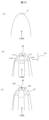
- FIG. 14 is a diagram showing the process of forming the electron emitting surface at the tip of the tip in Examples 2 and 3.
- FIG. 14(a) is a perspective view showing the tip end shape of the tip after electrolytic polishing
- FIG. 14(b) is a perspective view showing the tip end shape of the tip after the first stage thermal electric field treatment.
- FIG. 14(c) is a perspective view showing the shape of the tip after the second stage thermal electric field treatment.
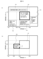
- FIG. 15 is a diagram showing the process condition range of the manufacturing method of Example 2, in which (a) of FIG. 15 shows the process condition range of the first stage thermal electric field treatment, and (b) of FIG.
- FIG. 3 is a diagram showing a range of process conditions for thermal electric field treatment in stages.
- a hexaboride single crystal field emission electron source 100 whose longitudinal direction is [100] oriented and whose tip is electrolytically polished to form a tip 6 is shown in FIG. 14(a).
- a first (100) top facet 42 is formed.
- the ⁇ n11 ⁇ plane of a hexaboride single crystal has a higher work function than ⁇ n10 ⁇ , the total area of the side facets of the ⁇ n11 ⁇ plane > the total area of the side facets of ⁇ n10 ⁇ , so It is possible to reduce unnecessary current emitted off the optical axis from 41.
- the feature of this manufacturing method is that, as shown in the process area 151 of FIG. 15(a), an electric field of 1 to 4.5 ⁇ 10 9 V/m is applied with the tip 6 as positive polarity while heating at 1500 to 1700°C in vacuum.
- the method is to apply a thermal electric field treatment.
- FIG. 15(a) the effects of heating and electric field application in the first stage thermal electric field treatment will be specifically explained using FIG. 15(a).
- the hexaboride single crystal rod 5 is a high melting point material (LaB 6 : 2210°C, CeB 6 : 2190°C), but when heated to 700 to 1400°C in vacuum, atoms on the surface migrate as shown in process region 152. This causes reconstruction of the crystal plane, especially at the tip 6. In this case, there is a tendency for the (100) plane to grow at the top of the tip 6 and the ⁇ n10 ⁇ > ⁇ n11 ⁇ plane to grow at the sides. Further, when heated to 1500° C. or higher as in the process region 153, evaporation from the surface gradually progresses and the crystal structure of the surface collapses, and in the process region 154 of 1700° C. or higher, the evaporation becomes even more pronounced.
- heating at 1500 to 1700°C mainly plays the role of evaporation, and the tip 6 of the hexaboride single crystal is heated without any electric field applied or under a weak electric field of 1 ⁇ 10 9 V/m or less.
- the tip 6 becomes thinner while almost maintaining a similar shape to the shape created by electrolytic polishing.
- evaporation becomes intense and it becomes difficult to maintain a similar shape to the shape created by electrolytic polishing.
- evaporation on the surface of the tip 6 occurs only by heating the process area 153 to 1500 to 1700°C, but by applying an electric field with the tip 6 as positive polarity, field evaporation can also occur. get up.
- the characteristic of electric field evaporation is that, unlike evaporation by heating alone, the sharp part of the tip 6 is preferentially evaporated, so the tip of the tip 6 is processed into a nearly hemispherical shape as a whole. .
- the tip 6 heated to 1500 to 1700°C as in the process region 151 has a voltage of 1 to 4.5 ⁇ 10 9 V/m. It was found that when a strong electric field of 2 is applied, a build-up occurs in which a (100) plane is formed at the top of the tip 6. It was also found that the electric field that causes build-up has no polarity dependence, and that both positive and negative electric fields can build up the (100) plane.
- the applied electric field be of positive polarity, since there is a risk that the degree of vacuum decreases due to the generation of radiation-stimulated desorption gas and the tip is damaged by discharge.
- the top facet 42 of the (100) plane is A microcrystal with two top facets 43 was formed.
- the microcrystal forming the top facet of the second (100) plane has a cubic shape whose side surfaces are also formed by the ⁇ 100 ⁇ plane group, or a trapezoidal shape whose side surfaces are formed by the ⁇ 111 ⁇ plane group. .
- the heating temperature is increased to 1300 to 1500°C.
- the positive electric field was also lowered by more than half to 1 to 2.25 ⁇ 10 9 V/m.
- the heating temperature was lowered to 1300-1500°C to suppress the evaporation of CeB 6 , and the electric field was lowered to less than half to weaken the build-up effect.
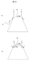
- FIG. 16 shows the structural changes that occur on the end surface of the first (100) top facet 42 of the tip 6 during the first-stage thermal electric field treatment in FIG. 15(a) and the second-stage thermal electric field treatment in FIG. 15(b). Shown in cross section.
- the build-up is caused by the amount of atomic diffusion toward the tip of the tip 6 due to the electrostatic force of the electric field F, which exceeds the amount of atomic diffusion toward the bottom of the tip 6 due to the temperature T. This occurs because atomic diffusion is promoted toward the top, and the growth of the (100) plane at the top and the side facets 41 of high-density crystal planes, especially the ⁇ 111 ⁇ plane, at the surrounding sides are promoted.
- the temperature was lowered to suppress the evaporation of CeB 6 , but if the temperature T is lowered too much, the amount of atomic diffusion on the surface toward the bottom of the tip 6 will also decrease, so it is preferable to lower it to 1300°C or less. do not have.
- the method for manufacturing the field emission electron source 100 can be summarized as follows.
- a high electric field with the tip 6 as positive polarity at high temperature to the tip 6 of a single crystal of hexaboride or transition metal carbide whose longitudinal direction is [100] oriented.
- Shifting buildup is caused to form the top facet 42 of the first (100) plane.
- a microcrystal having a second (100) top facet 43 is grown within the plane of the first (100) top facet 42. .
- a side consisting of four ⁇ n11 ⁇ planes and at least four ⁇ n10 ⁇ planes, and such that the total area of the side facets of ⁇ n11 ⁇ planes > the total area of the side facets of ⁇ n10 ⁇ forming a top facet 42 of a first (100) plane surrounded by facets, and further having a top facet 43 of a second (100) plane within the plane of the top facet 42 of the first (100) plane; Microcrystals could be formed.
- Transition metal carbide single crystals have a significantly higher melting point than hexaboride single crystals (HfC: 3890°C, ZrC: 3532°C, TiC: 3170°C, LaB 6 : 2210°C, CeB 6 : 2190°C), and their vapor pressure is also extremely high. Since the temperature is low, the process temperature and evaporation effect are different from those in Example 1, but the basic process concept is the same.
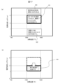
- FIG. 17 is a diagram showing the process condition range of the manufacturing method of Example 3, in which (a) of FIG. 17 shows the process condition range of the first stage thermal electric field treatment, and (b) of FIG. FIG. 3 is a diagram showing a range of process conditions for thermal electric field treatment in stages.
- the field emission electrons of the transition metal carbide single crystal whose tip was electrolytically polished to form a tip 6 as shown in FIG. 14(a) were applied.
- the source 100 is set in a vacuum chamber (not shown), and as shown in the process area 161 of FIG. Apply an electric field of 6 ⁇ 10 9 V/m.
- transition metal single crystal has the same tip structure as the hexaboride single crystal is that it is a compound that has the same cubic crystal structure as the hexaboride single crystal, and when it is built up, the surface energy This is because the geometric relationships between the side facets 41 and the top facets 42, which are stable, are similar. However, due to the difference in melting point, it is necessary to apply a higher temperature and higher electric field than the hexaboride single crystal tip.
- the second thermal electric field treatment was performed while heating at a temperature of 1500 to 1800°C and applying a positive electric field of less than half to 1 to 3 ⁇ 10. It was lowered to 9 V/m.
- the amount of atomic diffusion toward the bottom of the tip 6 due to the temperature T is greater than the amount of atomic diffusion on the surface toward the tip of the tip 6 due to the electrostatic force of the electric field F, and the top facet 42 of the first (100) plane
- a step was generated in the (100) plane, and a microcrystal having a second top facet 43 of the (100) plane within the plane of the first top facet 42 was formed.
- the electron emission characteristics of the field emission electron source produced according to the present invention will be described.
- the first top (100) facet 42 has a square shape of 170 nm in length x 170 nm in width
- the size of the microcrystals constituting the second top (100) facet 43 has a size of 50 nm in length x 50 nm in width x height.
- HfC a transition metal carbide single crystal with a cubic shape of 50 nm in diameter.
- Fig. 18(a) shows a field emission microscope image (FEM) from the HfC field emission electron source produced in the steps up to the first thermal electric field treatment in Fig. 17(a).
- FEM field emission microscope image
- the tip 6 manufactured in the first thermal electric field treatment step of FIG. 17(a) has an area of Since it is wide and flat, it is difficult for an electric field to be applied to it, and the amount of emitted current is relatively small, making it dark.
- the tip manufactured by performing the steps up to the second thermal electric field treatment in FIG. 17(b) has a top facet 42 of the first (100) plane. Since the electric field is concentrated on the (100) plane of the second top facet 43 formed of microcrystals formed in the plane, the center of the tip becomes relatively bright. On the other hand, the facet 42 of the first top (100) plane serving as the base and the side facets from the ⁇ n10 ⁇ plane around it have a relatively lower electric field strength and become dark.
- FIG. 19 shows a tip 6 in which only the first (100) facet 42 of FIG. 18(a) is formed, and a microcrystal having the second (100) facet 43 of the present invention in FIG. 18(b) is formed.
- This is a comparison of the radiation angular current density J ⁇ ( ⁇ A/sr) per total current It ( ⁇ A) of tip 6.
- Line 1900 is the radiation angular current density J ⁇ ( ⁇ A/sr) per total current It ( ⁇ A) of the tip 6 of the field emission source with only the first (100) facet 42.
- a line 1901 is the radiation angular current density J ⁇ ( ⁇ A/sr) per total current It ( ⁇ A) of the tip 6 of the field emission electron source having the second (100) facet 43 microcrystal.
- Tip 6 of the present invention is that, as shown by line 1901, J ⁇ /It is enhanced by about 4 times over 12, and a large radiation angular current density J ⁇ ( ⁇ A/sr ) can be obtained.
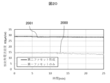
- FIG. 20 shows a field emission electron source in which only the facet 42 is formed on the first top (100) surface of FIG.
- the tip with only the first top (100) facet 42 has an initial value of J ⁇ ( ⁇ A/sr) of 14 ⁇ A/sr, and the electric field where the microcrystal with the second (100) facet 43 is formed.
- the emission electron source was set to 28 ⁇ A/sr, which is twice as high.
- a field emission electron source in which only the facet 42 of the first top (100) plane is formed has noise in the emission current, as shown by line 2000, and the noise increases with time, and the emission current decreases. I will do it.
- the field emission electron source in which a microcrystal with a second (100) facet 43 is formed has a high initial value of J ⁇ ( ⁇ A/sr), which is twice as large. Despite this, there is almost no current noise and the current is stable with no decrease.
- a field emission electron source in which a microcrystal with a second apex (100) facet 43 is formed is different from a field emission source in which only a first apex (100) facet 42 is formed.
- J ⁇ /It is four times higher, so even if it outputs twice as much J ⁇ ( ⁇ A/sr), only half the total current It ( ⁇ A) is required, and the electron beam-stimulated desorption gas generated from the electrode is halved. This reduces the electron beam stimulated desorption gas incident on the facet 43 of the second top (100) surface by half.
- the step of the microcrystals forming the second top (100) facet 43 acts as a diffusion barrier when the gas adsorbed on the side wall of the tip 6 diffuses toward the top of the tip 6. It is also possible that this becomes a trap site for the adsorbed gas, making it difficult for the adsorbed gas to reach the facet 43 of the second top (100) surface.
- J ⁇ ( ⁇ A/sr) the radiation angular current density required for electron microscopy.
- the size of the microcrystals (here defined as the length of one side of the (100) facet of the microcrystals) is controlled by the electric field, temperature, and holding time applied in the second thermal electric field treatment in Examples 2 and 3. It is possible to do so. Therefore, in this example, we investigated the change in electron emission characteristics depending on the size of the microcrystals formed within the facet 42 of the first apex (100) plane, and determined the optimal microcrystal size, height, and The results of determining the relationship between the size of the facet 42 on the top (100) surface and the size of the facet 43 on the second top (100) surface will be explained.
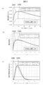
- FIG. 21 is a graph showing changes in the electron emission characteristics of the field emission electron source depending on the size (length of one side) of the microcrystal having the second (100) top facet of Example 5.
- FIG. 21(a) is a graph showing changes in the electric field strength at the center of the tip
- FIG. 21(b) is a graph showing changes in the radiation angular current density J ⁇ ( ⁇ A/sr)
- FIG. 21(c) is a graph showing changes in the electric field strength at the center of the tip. is a graph showing changes in light source diameter.
- FIG. 21 shows that the electric field strength at the center of the tip of the tip 6 (FIG. 21( a)), the radiation angular current density (FIG. 21(b)), and the light source diameter when used in an electron microscope (FIG. 21(c)).
- the size of the (100) plane in the first top facet 42 is 170 nm, which is the same as in Example 4 (square shape of 170 nm in length x 170 nm in width).
- the extraction voltage is 2 kV.
- the electric field strength at the center of the tip of the tip 6 when only the first (100) top facet 42 is formed without microcrystals is approximately 1.5 ⁇ 10 9 V/m.
- the electric field strength at the center of the tip 6 of the second (100) top facet 43 increases, and as the size of the microcrystals increases to 20 It was found that it reached 3.2 ⁇ 10 9 V/m at nm and then gradually decreased.
- the radiation angular current density J ⁇ ( ⁇ A/sr) shown in FIG. 21(b) reached a maximum of 93 ⁇ A/sr when the size of the microcrystals of the second (100) top facet 43 was 30 nm.
- the reason why the size of the microcrystal at which the electric field strength and radiation angular current density J ⁇ ( ⁇ A/sr) are maximum differs slightly is because of the facet 43 of the second top (100) plane, which becomes the electron emission surface even when the electric field strength is strong. This is because if the area of is small, the radiation angular current density J ⁇ that can be taken out will be small.
- FIG. 21(c) shows how the light source diameter of the field emission electron source changes with the size of the microcrystal of the second (100) top facet 43.
- the smaller the size of the microcrystal the smaller the light source diameter becomes, and the resolution of the electron microscope improves.
- electrons are emitted from the relatively large first top (100) facet 42, so the light source diameter becomes large.
- FIG. 21 shows how the electric field changes when the height of the microcrystal changes when the microcrystal size (defined here as the length of one side of the facet 43 of the second top (100) plane) is 30 nm.
- FIG. 22 shows the results of examining whether the radiation angular current density J ⁇ ( ⁇ A/sr) changes.
- FIG. 22 is a graph showing changes in the electron emission characteristics of the field emission electron source depending on the ratio of the height of the microcrystal to the length of one side of the top facet of the second (100) plane in Example 5.
- 22(a) is a graph showing changes in electric field strength at the center of the tip
- FIG. 22(b) is a graph showing changes in radiation angular current density J ⁇ ( ⁇ A/sr). Further, in FIGS. 22(a) and 22(b), the extraction voltage is 2 kV.
- the height of the microcrystals of the second (100) top facet 43 is determined by the size of the microcrystals ( It can be seen that it is preferable that the length is at least 0.7 times the length of one side.
- FIG. 23 shows the results of examining the relationship between the case where one side of the top facet of the first (100) plane in Example 5 is 170 nm and 340 nm.
- FIG. 23(a) is a diagram showing changes in the electric field strength at the center of the tip depending on the size (length of one side) of a microcrystal having a top facet of the second (100) plane.
- FIGS. 23(a) to 23(c) the extraction voltage is 3 kV.
- Figure 23(a) shows the case where the size (length of one side) of the first (100) top facet 42 is 170 nm (line 2301) and the case where the size (length of one side) of the first (100) top facet 42 is 170 nm (line 2301).
- the graph shows the dependence of the electric field strength applied to tip 6 on the size (length of one side) of the microcrystal when 340 nm (line 2302) is twice that (line 2302). It can be seen that as the size of the first (100) top facet 42 of the base increases, electric field concentration becomes less likely to occur even with the same microcrystal size, and thus the electric field strength decreases.
- the results of examining the normalized electric field strength with respect to the ratio of the size (length of one side) of the first (100) top facet 42 and the size (length of one side) of the microcrystal of the second top facet 43 are as follows. It is shown in FIG. 23(b). Line 2303 shows the case where the first (100) top facet 42 has a size of 170 nm, and line 2304 shows the case where the first (100) top facet 42 has a size of 340 nm.
- the change in the electric field intensity ratio is approximately determined by the ratio of the size of the facet 42 on the first top (100) plane to the size of the facet 43 on the second top (100) plane of the microcrystal.
- Figure 23(c) shows the size (length of one side) of the first (100) top facet 42 of the radiation angular current density J ⁇ ( ⁇ A/sr) and the microcrystal of the second top (100) facet 43. shows the dependence on the ratio of the size (length of one side).
- Line 2305 shows the case where the first (100) top facet 42 has a size of 170 nm
- line 2306 shows the case where the first (100) top facet 42 has a size of 340 nm.
- the extraction voltage is 2 kV
- the size of the first top (100) facet 42 is 340 nm
- the extraction voltage is 3.2 kV.
- the extraction voltages are different in this way, if the ratio of the size of the first (100) top facet 42 to the size of the microcrystals of the second top (100) facet 43 is 0.05 to 0.35, then the second It can be seen that the effect of electric field concentration due to the microcrystals of the facet 43 on the top (100) plane can be effectively utilized. Furthermore, if the ratio of the size of the first (100) top facet 42 to the size of the microcrystals of the second top (100) facet 43 is set to 0.1 to 0.25, the J ⁇ / It (ratio of radial angular current density J ⁇ ( ⁇ A/sr) to total current It ( ⁇ A)) is obtained.
- J ⁇ /It is approximately four times that of the conventional method. is obtained, which is particularly preferable.
- the size (length of one side) of the microcrystal of the facet 43 on the second apex (100) plane is preferably in the range of 10 to 60 nm, more preferably 20 to 40 nm, and particularly 30 nm.
- the height of the microcrystal of the facet 43 on the second apex (100) plane is suitably 0.7 times or more the vertical and horizontal size (length of one side) of the microcrystal.
- the ratio of the size (length of one side) of the microcrystal of facet 43 on the second (100) top surface to the size (length of one side) of facet 42 on the first (100) top surface of the base is 0.05 to A range of 0.35 is suitable, and a range of 0.1 to 0.25, particularly 0.15 to 0.2 is suitable.
- the microcrystal forming the top facet 43 of the second (100) plane has a cubic shape whose side surfaces are also formed by the ⁇ 100 ⁇ plane group, or a trapezoidal shape whose side surfaces are formed by the ⁇ 111 ⁇ plane group. be.
- Examples 2 to 5 above the case where the first top (100) facet 42 serving as the base is one stage has been described. In fact, it is also possible to create the first top (100) facet 42 in a multi-stage structure by changing the electric field, temperature, and holding time applied in the second thermal electric field treatment in Examples 2 and 3.
- the first top (100) facet 42 has a multi-stage structure, the number of stages of the diffusion barrier for the adsorbed gas diffusing through the side wall of the tip 6 increases, which has the effect of further improving the stability of the emission current.
- FIG. 24 is a perspective view of a tip in which the first apex (100) facet of the tip of Example 6 is formed in a multi-stage structure.
- FIG. 24 shows a structural diagram of a field emission electron source in which the first top (100) facet 42 has two stages.
- the size (length of one side) of the microcrystal of the second top (100) facet 43 at the top is preferably in the range of 10 to 60 nm, further 20 to 40 nm, In particular, 30 nm is suitable, and the ratio of the size of the second (100) top facet 43 of the topmost microcrystal to the size of the first (100) top facet 42 of the base is preferably in the range of 0.05 to 0.35. A range of 0.1 to 0.25, particularly 0.15 to 0.2 is appropriate.
- the size of the bottom (100) facet 42 increases and the diameter of the tip 6 becomes thicker.
- the size of the microcrystals of the second (100) top facet 43 is the smallest in the optimal range of 10 nm, and the size of the second (100) top facet 43 is the smallest in the optimal range. Even if the size ratio of the microcrystals is set to 0.35, which is the largest, the diameter of the tip 6 will exceed 1.5 ⁇ m if there are five or more stages.
- the extraction voltage required to obtain field emission electrons becomes too high, making it difficult to operate in an electron microscope due to restrictions on the high-voltage power supply used in the electron microscope and limitations on the withstand voltage between the electrodes. Therefore, it is appropriate that the number of stages of the first (100) top facet 42 be four stages or less.
- FIG. 25 is a schematic cross-sectional view of an electron beam apparatus (scanning electron microscope equipped with a field emission electron source using a hexaboride single crystal or transition metal carbide tip of the present invention) according to Example 7.
- Example 7 an electron source (field emission electron source) 100 using the facet 43 of the second top (100) plane of the tip 6 of the HfC transition metal carbide single crystal evaluated in Example 4 as the electron emission surface was used. An example of the installed scanning electron microscope 1000 is shown. Although not mentioned in this embodiment, similar effects can be obtained when a hexaboride single crystal such as CeB 6 is used.
- FIG. 25 shows a schematic diagram of a scanning electron microscope 1000, which is an electron beam apparatus according to Example 7.
- the field emission electron source 100 is constantly heated by passing a constant current through a heating power supply 103 controlled by a computer 101 and a controller 102, and an extraction power supply 104 supplies electricity to the extraction electrode 105 and to the tip 6 of the field emission electron source 100.
- a positive voltage is applied to emit electrons by field emission.
- the emitted electron beam 106 is accelerated toward the grounded anode 108 by a negative high voltage applied by an accelerating power source 107, and is then accelerated through a first condenser lens 109, an aperture 110, a second condenser lens 111, an objective lens 112,
- the secondary electrons are focused by the astigmatism correction coil 113, scanned by the deflection scanning coil 114, and irradiated onto the observation area on the sample 115, and the generated secondary electrons are detected by the secondary electron detector 116.
- Detectors other than a secondary electron detector are not shown in the figure, but a backscattered electron detector and an elemental analyzer are also used.
- the scanning electron microscope 1000 includes a field emission electron source 100, a sample stage 117 on which a sample 115 is placed, and a sample on the sample stage 117 that focuses electrons emitted from the field emission electron source 100 into a beam. It is equipped with an electron optical system that irradiates 115.
- Electrons are emitted from a field emission electron source 100 that uses the (100) plane of the HfC tip 6 as an electron emission surface.
- the emitted electrons have a narrow full width at half maximum energy and good monochromaticity because the work function of HfC is about 3.3 eV, which is lower than the 4.3 eV of a field emission electron source using a W ⁇ 310 ⁇ plane. . Therefore, chromatic aberration in the objective lens 112 and the like is reduced, and the sample 115 can be irradiated with a more focused electron beam 106. Thereby, a high-resolution scanning electron microscope image can be obtained.
- CeB 6 the work function is about 2.6 eV, which is lower than 4.3 eV for a field emission electron source using W ⁇ 310 ⁇ planes, so a similar effect can be obtained even narrower.
- the field emission electron source 100 of the present invention electrons are emitted from the facet 43 of the second top (100) surface of the microcrystal, which has a small area, so the light source has a small diameter and contributes to improved resolution.
- J ⁇ /It ratio of radiation angular current density J ⁇ ( ⁇ A/sr) to total current It ( ⁇ A)
- J ⁇ /It ratio of radiation angular current density J ⁇ ( ⁇ A/sr) to total current It ( ⁇ A)
- the step of the microcrystals acts as a barrier to the adsorbed gas diffusing on the side wall of the tip 6, which delays the adsorbed gas from reaching the facet 43 on the second top (100) surface, which reduces the electric field.
- the stability of the emission electron source 100 can be further improved. Therefore, the interval between flushing treatments necessary for cleaning the surface of the field emission electron source 100 can be extended, and stable measurements can be performed over a long period of time.
- the field emission electron source 100 of the present invention has J ⁇ /It that is more than four times higher than that of conventional electron sources, it is also possible to generate a large radiation angular current density.
- a large radiation angular current density is necessary and effective in order to shorten the analysis time.
Landscapes
- Engineering & Computer Science (AREA)
- Manufacturing & Machinery (AREA)
- Chemical & Material Sciences (AREA)
- Analytical Chemistry (AREA)
- Cold Cathode And The Manufacture (AREA)
- Crystals, And After-Treatments Of Crystals (AREA)
Abstract
Description
Claims (12)
- <100>軸の六ホウ化物単結晶または遷移金属炭化物単結晶のティップの先端に、n=1,2,3の整数とする少なくとも4面の{n11}面と、少なくとも4面の{ n10 }面から構成され、かつ{ n11 }面の側部ファセットの合計面積 > { n10 }の側部ファセットの合計面積であるような側部ファセットに囲まれた第一の(100)面の頂部ファセットを形成し、さらに該第一の(100)面の頂部ファセット面内に第二の(100)面の頂部ファセットを持つ微小結晶を形成し、主に該第二の(100)面の頂部ファセットから電子を放出する、ことを特徴とする電界放出電子源。
- 請求項1に記載の電界放出電子源であって、
前記六ホウ化物単結晶はLaB6またはCeB6を主成分とする単結晶である、ことを特徴とする電界放出電子源。 - 請求項1に記載の電界放出電子源であって、
前記遷移金属炭化物単結晶はHfC、またはZrC、またはTiCを主成分とする単結晶ある、ことを特徴とする電界放出電子源。 - 請求項1に記載の電界放出電子源であって、
前記六ホウ化物単結晶または前記遷移金属炭化物単結晶のティップの前記{ n11 }面は前記{ n10 }面より仕事関数が高い、ことを特徴とする電界放出電子源。 - 請求項1に記載の電界放出電子源であって、
前記微小結晶の前記第二の(100)面の頂部ファセットは、前記第一の(100)面の頂部ファセットより小さい、ことを特徴とする電界放出電子源。 - 請求項1に記載の電界放出電子源であって、
前記微小結晶は、頂部および側部が{100}面で構成される立方体形状、または、頂部ファセットが(100)面で側部が{111}面で構成される台形形状である、ことを特徴とする電界放出電子源。 - 請求項1に記載の電界放出電子源であって、
前記微小結晶の前記第二の(100)面の頂部ファセットの一辺の長さと、前記第一の(100)面の頂部ファセットの一辺の長さの比が0.05~0.35の範囲である、ことを特徴とする電界放出電子源。 - 請求項1に記載の電界放出電子源であって、
前記微小結晶の前記第二の(100)面の頂部ファセットの一辺の長さは、10~60 nmの範囲である、ことを特徴とする電界放出電子源。 - 請求項1に記載の電界放出電子源であって、
前記微小結晶の高さは、前記第二の(100)面の頂部ファセットの一辺の長さの0.7倍以上である、ことを特徴とする電界放出電子源。 - 請求項1に記載の電界放出電子源であって、
前記第一の(100)面の頂部のファセットが4段以下の多段構造である、ことを特徴とする電界放出電子源。 - 六ホウ化物または遷移金属炭化物の長手方向が[100]方位の単結晶のティップに対し、高温で、ティップを正極性とした高電界を印加することにより、前記ティップの先端に向かう原子の移動によるビルドアップを引き起こして第一の(100)面の頂部ファセットを形成した後、前記ティップに印加する電界を低下させることにより、前記第一の(100)面の頂部ファセットの面内に、第二の(100)面の頂部ファセットを持つ微小結晶を成長させる、電界放出電子源の製造方法。
- 電子源と、試料を載置する試料台と、前記電子源から放出された電子をビーム状に収束させて前記試料台の上の試料に照射する電子光学系とを備えた電子線装置であって、
前記電子源は、<100>軸の六ホウ化物単結晶または遷移金属炭化物単結晶のティップの先端に、n=1,2,3の整数とする少なくとも4面の{n11}面と、少なくとも4面の{ n10 }面から構成され、かつ{ n11 }面の側部ファセットの合計面積 > { n10 }の側部ファセットの合計面積であるような側部ファセットに囲まれた第一の(100)面の頂部ファセットを形成し、さらに該第一の(100)面の頂部ファセット面内に第二の(100)面の頂部ファセットを持つ微小結晶を形成し、該第二の(100)面の頂部ファセットから電子を放出する電界放出電子源を備える、ことを特徴とする電子線装置。
Priority Applications (4)
| Application Number | Priority Date | Filing Date | Title |
|---|---|---|---|
| JP2024528084A JP7733825B2 (ja) | 2022-06-20 | 2022-06-20 | 電界放出電子源とその製造方法およびそれを用いた電子線装置 |
| US18/865,028 US20250316438A1 (en) | 2022-06-20 | 2022-06-20 | Field emission electron source, method of producing same, and electron beam device using same |
| PCT/JP2022/024469 WO2023248271A1 (ja) | 2022-06-20 | 2022-06-20 | 電界放出電子源とその製造方法およびそれを用いた電子線装置 |
| CN202280095706.3A CN119137705A (zh) | 2022-06-20 | 2022-06-20 | 场致发射电子源及其制造方法和使用该制造方法的电子束装置 |
Applications Claiming Priority (1)
| Application Number | Priority Date | Filing Date | Title |
|---|---|---|---|
| PCT/JP2022/024469 WO2023248271A1 (ja) | 2022-06-20 | 2022-06-20 | 電界放出電子源とその製造方法およびそれを用いた電子線装置 |
Publications (1)
| Publication Number | Publication Date |
|---|---|
| WO2023248271A1 true WO2023248271A1 (ja) | 2023-12-28 |
Family
ID=89379562
Family Applications (1)
| Application Number | Title | Priority Date | Filing Date |
|---|---|---|---|
| PCT/JP2022/024469 Ceased WO2023248271A1 (ja) | 2022-06-20 | 2022-06-20 | 電界放出電子源とその製造方法およびそれを用いた電子線装置 |
Country Status (4)
| Country | Link |
|---|---|
| US (1) | US20250316438A1 (ja) |
| JP (1) | JP7733825B2 (ja) |
| CN (1) | CN119137705A (ja) |
| WO (1) | WO2023248271A1 (ja) |
Citations (3)
| Publication number | Priority date | Publication date | Assignee | Title |
|---|---|---|---|---|
| JP2008177017A (ja) * | 2007-01-18 | 2008-07-31 | Sumitomo Electric Ind Ltd | 電子源用チップ及びその製造方法 |
| JP2010251087A (ja) * | 2009-04-15 | 2010-11-04 | Sumitomo Electric Ind Ltd | 冷陰極電界放出電子銃 |
| WO2022064557A1 (ja) * | 2020-09-23 | 2022-03-31 | 株式会社日立ハイテク | 電子源とその製造方法およびそれを用いた電子線装置 |
-
2022
- 2022-06-20 CN CN202280095706.3A patent/CN119137705A/zh active Pending
- 2022-06-20 US US18/865,028 patent/US20250316438A1/en active Pending
- 2022-06-20 JP JP2024528084A patent/JP7733825B2/ja active Active
- 2022-06-20 WO PCT/JP2022/024469 patent/WO2023248271A1/ja not_active Ceased
Patent Citations (3)
| Publication number | Priority date | Publication date | Assignee | Title |
|---|---|---|---|---|
| JP2008177017A (ja) * | 2007-01-18 | 2008-07-31 | Sumitomo Electric Ind Ltd | 電子源用チップ及びその製造方法 |
| JP2010251087A (ja) * | 2009-04-15 | 2010-11-04 | Sumitomo Electric Ind Ltd | 冷陰極電界放出電子銃 |
| WO2022064557A1 (ja) * | 2020-09-23 | 2022-03-31 | 株式会社日立ハイテク | 電子源とその製造方法およびそれを用いた電子線装置 |
Also Published As
| Publication number | Publication date |
|---|---|
| CN119137705A (zh) | 2024-12-13 |
| JPWO2023248271A1 (ja) | 2023-12-28 |
| JP7733825B2 (ja) | 2025-09-03 |
| US20250316438A1 (en) | 2025-10-09 |
Similar Documents
| Publication | Publication Date | Title |
|---|---|---|
| US10707046B2 (en) | Electron source and electron beam device using the same | |
| JP3832402B2 (ja) | カーボンナノチューブを有する電子源とそれを用いた電子顕微鏡および電子線描画装置 | |
| JP5301168B2 (ja) | 冷電界エミッタ | |
| US10586674B2 (en) | Field emission electron source, method for manufacturing same, and electron beam device | |
| JP7403678B2 (ja) | 電子源とその製造方法およびそれを用いた電子線装置 | |
| CN109804450B (zh) | 电子束装置 | |
| US4486684A (en) | Single crystal lanthanum hexaboride electron beam emitter having high brightness | |
| WO2004070766A1 (ja) | 電子源 | |
| JP7733825B2 (ja) | 電界放出電子源とその製造方法およびそれを用いた電子線装置 | |
| Mousa et al. | Investigating of the field emission performance on nano-apex carbon fiber and tungsten tips | |
| JP7295974B2 (ja) | 電子源、電子線装置および電子源の製造方法 | |
| WO2015058588A1 (zh) | 针状带电粒子束发射体及制作方法 | |
| JP7022837B2 (ja) | 電子源とその製造方法およびそれを用いた電子線装置 | |
| JP2003007195A (ja) | 電子放射陰極及びその製造方法 | |
| CN1193397C (zh) | 弹道电子发射源及其制备方法 | |
| JP2009187739A (ja) | 電界放出型電子源及びその製造方法 | |
| WO2025253467A1 (ja) | ショットキー電子源、ショットキー電子源の製造方法および電子線装置 | |
| JP4874758B2 (ja) | 電子源 | |
| Fratini et al. | Carbon-nanotubes field emitter to be used in advanced X-ray source | |
| JP2010067452A (ja) | 電子放射陰極、電子顕微鏡および電子ビーム露光機 | |
| JP2010238670A (ja) | 電子放射陰極の製造方法 |
Legal Events
| Date | Code | Title | Description |
|---|---|---|---|
| 121 | Ep: the epo has been informed by wipo that ep was designated in this application |
Ref document number: 22947835 Country of ref document: EP Kind code of ref document: A1 |
|
| ENP | Entry into the national phase |
Ref document number: 2024528084 Country of ref document: JP Kind code of ref document: A |
|
| WWE | Wipo information: entry into national phase |
Ref document number: 202280095706.3 Country of ref document: CN |
|
| WWE | Wipo information: entry into national phase |
Ref document number: 18865028 Country of ref document: US |
|
| NENP | Non-entry into the national phase |
Ref country code: DE |
|
| 122 | Ep: pct application non-entry in european phase |
Ref document number: 22947835 Country of ref document: EP Kind code of ref document: A1 |
|
| WWP | Wipo information: published in national office |
Ref document number: 18865028 Country of ref document: US |