WO2023242664A1 - 半導体装置、記憶装置 - Google Patents
半導体装置、記憶装置 Download PDFInfo
- Publication number
- WO2023242664A1 WO2023242664A1 PCT/IB2023/055668 IB2023055668W WO2023242664A1 WO 2023242664 A1 WO2023242664 A1 WO 2023242664A1 IB 2023055668 W IB2023055668 W IB 2023055668W WO 2023242664 A1 WO2023242664 A1 WO 2023242664A1
- Authority
- WO
- WIPO (PCT)
- Prior art keywords
- insulator
- conductor
- oxide
- transistor
- region
- Prior art date
- Legal status (The legal status is an assumption and is not a legal conclusion. Google has not performed a legal analysis and makes no representation as to the accuracy of the status listed.)
- Ceased
Links
Images


Classifications
-
- H—ELECTRICITY
- H10—SEMICONDUCTOR DEVICES; ELECTRIC SOLID-STATE DEVICES NOT OTHERWISE PROVIDED FOR
- H10B—ELECTRONIC MEMORY DEVICES
- H10B53/00—Ferroelectric RAM [FeRAM] devices comprising ferroelectric memory capacitors
- H10B53/20—Ferroelectric RAM [FeRAM] devices comprising ferroelectric memory capacitors characterised by the three-dimensional [3D] arrangements, e.g. with cells on different height levels
-
- H—ELECTRICITY
- H10—SEMICONDUCTOR DEVICES; ELECTRIC SOLID-STATE DEVICES NOT OTHERWISE PROVIDED FOR
- H10D—INORGANIC ELECTRIC SEMICONDUCTOR DEVICES
- H10D64/00—Electrodes of devices having potential barriers
- H10D64/60—Electrodes characterised by their materials
- H10D64/66—Electrodes having a conductor capacitively coupled to a semiconductor by an insulator, e.g. MIS electrodes
- H10D64/68—Electrodes having a conductor capacitively coupled to a semiconductor by an insulator, e.g. MIS electrodes characterised by the insulator, e.g. by the gate insulator
- H10D64/693—Electrodes having a conductor capacitively coupled to a semiconductor by an insulator, e.g. MIS electrodes characterised by the insulator, e.g. by the gate insulator the insulator comprising nitrogen, e.g. nitrides, oxynitrides or nitrogen-doped materials
-
- H—ELECTRICITY
- H10—SEMICONDUCTOR DEVICES; ELECTRIC SOLID-STATE DEVICES NOT OTHERWISE PROVIDED FOR
- H10B—ELECTRONIC MEMORY DEVICES
- H10B12/00—Dynamic random access memory [DRAM] devices
-
- H—ELECTRICITY
- H10—SEMICONDUCTOR DEVICES; ELECTRIC SOLID-STATE DEVICES NOT OTHERWISE PROVIDED FOR
- H10B—ELECTRONIC MEMORY DEVICES
- H10B41/00—Electrically erasable-and-programmable ROM [EEPROM] devices comprising floating gates
- H10B41/70—Electrically erasable-and-programmable ROM [EEPROM] devices comprising floating gates the floating gate being an electrode shared by two or more components
-
- H—ELECTRICITY
- H10—SEMICONDUCTOR DEVICES; ELECTRIC SOLID-STATE DEVICES NOT OTHERWISE PROVIDED FOR
- H10B—ELECTRONIC MEMORY DEVICES
- H10B53/00—Ferroelectric RAM [FeRAM] devices comprising ferroelectric memory capacitors
- H10B53/10—Ferroelectric RAM [FeRAM] devices comprising ferroelectric memory capacitors characterised by the top-view layout
-
- H—ELECTRICITY
- H10—SEMICONDUCTOR DEVICES; ELECTRIC SOLID-STATE DEVICES NOT OTHERWISE PROVIDED FOR
- H10B—ELECTRONIC MEMORY DEVICES
- H10B53/00—Ferroelectric RAM [FeRAM] devices comprising ferroelectric memory capacitors
- H10B53/30—Ferroelectric RAM [FeRAM] devices comprising ferroelectric memory capacitors characterised by the memory core region
-
- H—ELECTRICITY
- H10—SEMICONDUCTOR DEVICES; ELECTRIC SOLID-STATE DEVICES NOT OTHERWISE PROVIDED FOR
- H10D—INORGANIC ELECTRIC SEMICONDUCTOR DEVICES
- H10D1/00—Resistors, capacitors or inductors
- H10D1/60—Capacitors
- H10D1/62—Capacitors having potential barriers
- H10D1/66—Conductor-insulator-semiconductor capacitors, e.g. MOS capacitors
-
- H—ELECTRICITY
- H10—SEMICONDUCTOR DEVICES; ELECTRIC SOLID-STATE DEVICES NOT OTHERWISE PROVIDED FOR
- H10D—INORGANIC ELECTRIC SEMICONDUCTOR DEVICES
- H10D30/00—Field-effect transistors [FET]
- H10D30/01—Manufacture or treatment
- H10D30/019—Manufacture or treatment of FETs having stacked nanowire, nanosheet or nanoribbon channels
- H10D30/0191—Manufacture or treatment of FETs having stacked nanowire, nanosheet or nanoribbon channels forming stacked channels, e.g. changing their shapes or sizes
-
- H—ELECTRICITY
- H10—SEMICONDUCTOR DEVICES; ELECTRIC SOLID-STATE DEVICES NOT OTHERWISE PROVIDED FOR
- H10D—INORGANIC ELECTRIC SEMICONDUCTOR DEVICES
- H10D30/00—Field-effect transistors [FET]
- H10D30/01—Manufacture or treatment
- H10D30/021—Manufacture or treatment of FETs having insulated gates [IGFET]
-
- H—ELECTRICITY
- H10—SEMICONDUCTOR DEVICES; ELECTRIC SOLID-STATE DEVICES NOT OTHERWISE PROVIDED FOR
- H10D—INORGANIC ELECTRIC SEMICONDUCTOR DEVICES
- H10D30/00—Field-effect transistors [FET]
- H10D30/60—Insulated-gate field-effect transistors [IGFET]
- H10D30/67—Thin-film transistors [TFT]
- H10D30/6729—Thin-film transistors [TFT] characterised by the electrodes
- H10D30/673—Thin-film transistors [TFT] characterised by the electrodes characterised by the shapes, relative sizes or dispositions of the gate electrodes
- H10D30/6733—Multi-gate TFTs
- H10D30/6734—Multi-gate TFTs having gate electrodes arranged on both top and bottom sides of the channel, e.g. dual-gate TFTs
-
- H—ELECTRICITY
- H10—SEMICONDUCTOR DEVICES; ELECTRIC SOLID-STATE DEVICES NOT OTHERWISE PROVIDED FOR
- H10D—INORGANIC ELECTRIC SEMICONDUCTOR DEVICES
- H10D30/00—Field-effect transistors [FET]
- H10D30/60—Insulated-gate field-effect transistors [IGFET]
- H10D30/67—Thin-film transistors [TFT]
- H10D30/674—Thin-film transistors [TFT] characterised by the active materials
- H10D30/6755—Oxide semiconductors, e.g. zinc oxide, copper aluminium oxide or cadmium stannate
-
- H—ELECTRICITY
- H10—SEMICONDUCTOR DEVICES; ELECTRIC SOLID-STATE DEVICES NOT OTHERWISE PROVIDED FOR
- H10D—INORGANIC ELECTRIC SEMICONDUCTOR DEVICES
- H10D30/00—Field-effect transistors [FET]
- H10D30/60—Insulated-gate field-effect transistors [IGFET]
- H10D30/67—Thin-film transistors [TFT]
- H10D30/6757—Thin-film transistors [TFT] characterised by the structure of the channel, e.g. transverse or longitudinal shape or doping profile
-
- H—ELECTRICITY
- H10—SEMICONDUCTOR DEVICES; ELECTRIC SOLID-STATE DEVICES NOT OTHERWISE PROVIDED FOR
- H10D—INORGANIC ELECTRIC SEMICONDUCTOR DEVICES
- H10D30/00—Field-effect transistors [FET]
- H10D30/60—Insulated-gate field-effect transistors [IGFET]
- H10D30/68—Floating-gate IGFETs
-
- H—ELECTRICITY
- H10—SEMICONDUCTOR DEVICES; ELECTRIC SOLID-STATE DEVICES NOT OTHERWISE PROVIDED FOR
- H10D—INORGANIC ELECTRIC SEMICONDUCTOR DEVICES
- H10D30/00—Field-effect transistors [FET]
- H10D30/60—Insulated-gate field-effect transistors [IGFET]
- H10D30/69—IGFETs having charge trapping gate insulators, e.g. MNOS transistors
-
- H—ELECTRICITY
- H10—SEMICONDUCTOR DEVICES; ELECTRIC SOLID-STATE DEVICES NOT OTHERWISE PROVIDED FOR
- H10D—INORGANIC ELECTRIC SEMICONDUCTOR DEVICES
- H10D64/00—Electrodes of devices having potential barriers
- H10D64/60—Electrodes characterised by their materials
- H10D64/66—Electrodes having a conductor capacitively coupled to a semiconductor by an insulator, e.g. MIS electrodes
- H10D64/68—Electrodes having a conductor capacitively coupled to a semiconductor by an insulator, e.g. MIS electrodes characterised by the insulator, e.g. by the gate insulator
- H10D64/691—Electrodes having a conductor capacitively coupled to a semiconductor by an insulator, e.g. MIS electrodes characterised by the insulator, e.g. by the gate insulator comprising metallic compounds, e.g. metal oxides or metal silicates
-
- H—ELECTRICITY
- H10—SEMICONDUCTOR DEVICES; ELECTRIC SOLID-STATE DEVICES NOT OTHERWISE PROVIDED FOR
- H10D—INORGANIC ELECTRIC SEMICONDUCTOR DEVICES
- H10D84/00—Integrated devices formed in or on semiconductor substrates that comprise only semiconducting layers, e.g. on Si wafers or on GaAs-on-Si wafers
- H10D84/01—Manufacture or treatment
- H10D84/0123—Integrating together multiple components covered by H10D12/00 or H10D30/00, e.g. integrating multiple IGBTs
- H10D84/0126—Integrating together multiple components covered by H10D12/00 or H10D30/00, e.g. integrating multiple IGBTs the components including insulated gates, e.g. IGFETs
- H10D84/0165—Integrating together multiple components covered by H10D12/00 or H10D30/00, e.g. integrating multiple IGBTs the components including insulated gates, e.g. IGFETs the components including complementary IGFETs, e.g. CMOS devices
-
- H—ELECTRICITY
- H10—SEMICONDUCTOR DEVICES; ELECTRIC SOLID-STATE DEVICES NOT OTHERWISE PROVIDED FOR
- H10D—INORGANIC ELECTRIC SEMICONDUCTOR DEVICES
- H10D84/00—Integrated devices formed in or on semiconductor substrates that comprise only semiconducting layers, e.g. on Si wafers or on GaAs-on-Si wafers
- H10D84/01—Manufacture or treatment
- H10D84/02—Manufacture or treatment characterised by using material-based technologies
- H10D84/03—Manufacture or treatment characterised by using material-based technologies using Group IV technology, e.g. silicon technology or silicon-carbide [SiC] technology
- H10D84/038—Manufacture or treatment characterised by using material-based technologies using Group IV technology, e.g. silicon technology or silicon-carbide [SiC] technology using silicon technology, e.g. SiGe
-
- H—ELECTRICITY
- H10—SEMICONDUCTOR DEVICES; ELECTRIC SOLID-STATE DEVICES NOT OTHERWISE PROVIDED FOR
- H10D—INORGANIC ELECTRIC SEMICONDUCTOR DEVICES
- H10D84/00—Integrated devices formed in or on semiconductor substrates that comprise only semiconducting layers, e.g. on Si wafers or on GaAs-on-Si wafers
- H10D84/80—Integrated devices formed in or on semiconductor substrates that comprise only semiconducting layers, e.g. on Si wafers or on GaAs-on-Si wafers characterised by the integration of at least one component covered by groups H10D12/00 or H10D30/00, e.g. integration of IGFETs
- H10D84/82—Integrated devices formed in or on semiconductor substrates that comprise only semiconducting layers, e.g. on Si wafers or on GaAs-on-Si wafers characterised by the integration of at least one component covered by groups H10D12/00 or H10D30/00, e.g. integration of IGFETs of only field-effect components
- H10D84/83—Integrated devices formed in or on semiconductor substrates that comprise only semiconducting layers, e.g. on Si wafers or on GaAs-on-Si wafers characterised by the integration of at least one component covered by groups H10D12/00 or H10D30/00, e.g. integration of IGFETs of only field-effect components of only insulated-gate FETs [IGFET]
- H10D84/83135—Integrated devices formed in or on semiconductor substrates that comprise only semiconducting layers, e.g. on Si wafers or on GaAs-on-Si wafers characterised by the integration of at least one component covered by groups H10D12/00 or H10D30/00, e.g. integration of IGFETs of only field-effect components of only insulated-gate FETs [IGFET] the IGFETs characterised by having different gate conductor materials or different gate conductor implants
-
- H—ELECTRICITY
- H10—SEMICONDUCTOR DEVICES; ELECTRIC SOLID-STATE DEVICES NOT OTHERWISE PROVIDED FOR
- H10D—INORGANIC ELECTRIC SEMICONDUCTOR DEVICES
- H10D84/00—Integrated devices formed in or on semiconductor substrates that comprise only semiconducting layers, e.g. on Si wafers or on GaAs-on-Si wafers
- H10D84/80—Integrated devices formed in or on semiconductor substrates that comprise only semiconducting layers, e.g. on Si wafers or on GaAs-on-Si wafers characterised by the integration of at least one component covered by groups H10D12/00 or H10D30/00, e.g. integration of IGFETs
- H10D84/82—Integrated devices formed in or on semiconductor substrates that comprise only semiconducting layers, e.g. on Si wafers or on GaAs-on-Si wafers characterised by the integration of at least one component covered by groups H10D12/00 or H10D30/00, e.g. integration of IGFETs of only field-effect components
- H10D84/83—Integrated devices formed in or on semiconductor substrates that comprise only semiconducting layers, e.g. on Si wafers or on GaAs-on-Si wafers characterised by the integration of at least one component covered by groups H10D12/00 or H10D30/00, e.g. integration of IGFETs of only field-effect components of only insulated-gate FETs [IGFET]
- H10D84/8314—Integrated devices formed in or on semiconductor substrates that comprise only semiconducting layers, e.g. on Si wafers or on GaAs-on-Si wafers characterised by the integration of at least one component covered by groups H10D12/00 or H10D30/00, e.g. integration of IGFETs of only field-effect components of only insulated-gate FETs [IGFET] the IGFETs characterised by having gate insulating layers with different properties
-
- H—ELECTRICITY
- H10—SEMICONDUCTOR DEVICES; ELECTRIC SOLID-STATE DEVICES NOT OTHERWISE PROVIDED FOR
- H10D—INORGANIC ELECTRIC SEMICONDUCTOR DEVICES
- H10D86/00—Integrated devices formed in or on insulating or conducting substrates, e.g. formed in silicon-on-insulator [SOI] substrates or on stainless steel or glass substrates
- H10D86/40—Integrated devices formed in or on insulating or conducting substrates, e.g. formed in silicon-on-insulator [SOI] substrates or on stainless steel or glass substrates characterised by multiple TFTs
- H10D86/60—Integrated devices formed in or on insulating or conducting substrates, e.g. formed in silicon-on-insulator [SOI] substrates or on stainless steel or glass substrates characterised by multiple TFTs wherein the TFTs are in active matrices
-
- H—ELECTRICITY
- H10—SEMICONDUCTOR DEVICES; ELECTRIC SOLID-STATE DEVICES NOT OTHERWISE PROVIDED FOR
- H10D—INORGANIC ELECTRIC SEMICONDUCTOR DEVICES
- H10D87/00—Integrated devices comprising both bulk components and either SOI or SOS components on the same substrate
-
- H—ELECTRICITY
- H10—SEMICONDUCTOR DEVICES; ELECTRIC SOLID-STATE DEVICES NOT OTHERWISE PROVIDED FOR
- H10P—GENERIC PROCESSES OR APPARATUS FOR THE MANUFACTURE OR TREATMENT OF DEVICES COVERED BY CLASS H10
- H10P14/00—Formation of materials, e.g. in the shape of layers or pillars
- H10P14/40—Formation of materials, e.g. in the shape of layers or pillars of conductive or resistive materials
-
- H—ELECTRICITY
- H10—SEMICONDUCTOR DEVICES; ELECTRIC SOLID-STATE DEVICES NOT OTHERWISE PROVIDED FOR
- H10W—GENERIC PACKAGES, INTERCONNECTIONS, CONNECTORS OR OTHER CONSTRUCTIONAL DETAILS OF DEVICES COVERED BY CLASS H10
- H10W20/00—Interconnections in chips, wafers or substrates
- H10W20/01—Manufacture or treatment
-
- H—ELECTRICITY
- H10—SEMICONDUCTOR DEVICES; ELECTRIC SOLID-STATE DEVICES NOT OTHERWISE PROVIDED FOR
- H10W—GENERIC PACKAGES, INTERCONNECTIONS, CONNECTORS OR OTHER CONSTRUCTIONAL DETAILS OF DEVICES COVERED BY CLASS H10
- H10W20/00—Interconnections in chips, wafers or substrates
- H10W20/40—Interconnections external to wafers or substrates, e.g. back-end-of-line [BEOL] metallisations or vias connecting to gate electrodes
Definitions
- one embodiment of the present invention is not limited to the above technical field.
- the technical fields of one embodiment of the present invention include semiconductor devices, display devices, light-emitting devices, power storage devices, storage devices, electronic devices, lighting devices, input devices (for example, touch sensors), input/output devices (for example, touch panels), An example of such a driving method or a manufacturing method thereof can be mentioned.
- a semiconductor device refers to any device that can function by utilizing semiconductor characteristics.
- Semiconductor elements such as transistors, semiconductor circuits, arithmetic devices, and storage devices are examples of semiconductor devices.
- Display devices liquid crystal display devices, light emitting display devices, etc.
- projection devices lighting devices, electro-optical devices, power storage devices, storage devices, semiconductor circuits, imaging devices, electronic equipment, and the like may be said to include semiconductor devices.
- a CPU is an assembly of semiconductor elements, including a semiconductor integrated circuit (at least a transistor and a memory) formed into a chip by processing a semiconductor wafer, and on which electrodes serving as connection terminals are formed.
- an object of one embodiment of the present invention is to provide a storage device with a large storage capacity.
- one of the challenges is to provide a storage device that operates at high speed.
- one of the challenges is to provide a storage device with low power consumption.
- one of the challenges is to provide a new storage device.
- Another object of the present invention is to provide a method for manufacturing a new storage device.
- the first laminate further includes a fifth insulator below the first insulator
- the second laminate further includes a sixth insulator on the third insulator.
- the fifth insulator further has oxygen permeability than the first insulator
- the sixth insulator further has oxygen permeability than the second insulator
- the fifth insulator further has It is preferable that each of the and the sixth insulator includes aluminum.
- the third insulator and the sixth insulator have a laminated structure, the laminated structure has an island shape, and in a cross-sectional view, the side edge part of the laminated structure is the semiconductor layer. It is preferable to coincide with the side edge of.
- Another embodiment of the present invention is a semiconductor device including a first stacked body, a semiconductor layer under the first stacked body, and a second stacked body under the semiconductor layer.
- the semiconductor layer has a first region, and a second region and a third region provided to sandwich the first region.
- the first stacked body and the second stacked body are provided symmetrically with respect to the first region.
- the first laminate includes a first insulator, a second insulator on the first insulator, and a third insulator on the second insulator.
- the second laminate includes a first metal oxide, a fourth insulator under the first metal oxide, and a fifth insulator under the fourth insulator.
- the first insulator is less permeable to oxygen than the second insulator.
- the third insulator is less permeable to hydrogen than the second insulator.
- the first metal oxide is less permeable to oxygen than the fourth insulator.
- the fifth insulator is less permeable to hydrogen than the fourth insulator.
- Each of the first insulator and the first metal oxide includes at least one of gallium and aluminum.
- Each of the second insulator and the fourth insulator includes silicon and oxygen.
- Each of the third insulator and the fifth insulator includes silicon and nitrogen.
- the semiconductor layer includes a second metal oxide, each of the first metal oxide and the second metal oxide includes indium, and indium in the first metal oxide
- the atomic ratio of at least one of gallium and aluminum to indium is preferably larger than the atomic ratio of at least one of gallium and aluminum to indium in the second metal oxide.
- the semiconductor device further includes a sixth insulator between the fourth insulator and the fifth insulator, and the sixth insulator has a function of capturing or fixing hydrogen. It is preferable.
- the semiconductor device further includes a seventh insulator between the second insulator and the third insulator, and the seventh insulator has a function of capturing or fixing hydrogen. It is preferable.
- the semiconductor device further includes a first conductor and a second conductor, the first conductor being located above the first laminate, and the second conductor comprising: Preferably, it is located below the second laminate.
- One embodiment of the present invention is a memory device including the above semiconductor device and a capacitor.
- the capacitive element is a ferroelectric capacitor.
- a semiconductor device having good electrical characteristics can be provided.
- a highly reliable semiconductor device can be provided.
- a semiconductor device with less variation in electrical characteristics of transistors can be provided.
- a semiconductor device that can be miniaturized or highly integrated can be provided.
- a semiconductor device with high operating speed can be provided.
- a semiconductor device with a large on-state current can be provided.
- a semiconductor device with low power consumption can be provided.
- a new semiconductor device can be provided.
- a method for manufacturing a semiconductor device with high productivity can be provided.
- a novel method for manufacturing a semiconductor device can be provided.
- a storage device with a large storage capacity can be provided.
- a storage device with high operating speed can be provided.
- a storage device with low power consumption can be provided.
- new storage devices can be provided.
- a novel method for manufacturing a semiconductor device can be provided.
- FIG. 1A is a top view showing an example of a semiconductor device.
- FIGS. 1B and 1C are cross-sectional views showing an example of a semiconductor device.
- 2A and 2B are cross-sectional views showing an example of a semiconductor device.
- FIG. 3A is a top view showing an example of a semiconductor device.
- 3B and 3C are cross-sectional views showing an example of a semiconductor device.
- 4A to 4D are cross-sectional views showing an example of a semiconductor device.
- 5A to 5D are cross-sectional views showing an example of a semiconductor device.
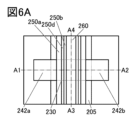
- FIG. 6A is a top view showing an example of a semiconductor device.
- 6B and 6C are cross-sectional views showing an example of a semiconductor device.
- FIG. 7A to 7D are cross-sectional views showing an example of a semiconductor device.
- FIG. 8A is a top view showing an example of a semiconductor device.
- FIGS. 8B and 8C are cross-sectional views showing an example of a semiconductor device.
- 9A to 9F are cross-sectional views showing an example of a semiconductor device.
- 10A to 10F are cross-sectional views showing an example of a semiconductor device.
- 11A to 11D are cross-sectional views showing an example of a semiconductor device.
- 12A to 12D are cross-sectional views showing an example of a semiconductor device.
- 13A to 13F are cross-sectional views showing an example of a semiconductor device.
- 14A to 14F are cross-sectional views showing an example of a semiconductor device.
- 15A is a top view showing an example of a semiconductor device.
- 15B to 15D are cross-sectional views showing an example of a semiconductor device.
- 16A and 16B are cross-sectional views showing an example of a semiconductor device.
- 17A and 17B are cross-sectional views showing an example of a semiconductor device.
- 18A and 18B are cross-sectional views showing an example of a semiconductor device.
- FIG. 19A is a top view showing an example of a semiconductor device.
- 19B and 19C are cross-sectional views showing an example of a semiconductor device.
- FIG. 20A is a top view showing an example of a semiconductor device.
- FIG. 20B is a cross-sectional view showing an example of a semiconductor device.
- FIG. 20A is a top view showing an example of a semiconductor device.
- FIG. 20B is a cross-sectional view showing an example of a semiconductor device.
- FIG. 20A is a top view showing an example of a semiconductor device.
- FIG. 21 is a cross-sectional view showing an example of a semiconductor device.
- FIG. 22 is a cross-sectional view showing an example of a semiconductor device.
- FIG. 23A is a top view showing an example of a semiconductor device.
- FIG. 23B is a cross-sectional view showing an example of a semiconductor device.
- FIG. 24A is a top view showing an example of a semiconductor device.
- FIG. 24B is a cross-sectional view showing an example of a semiconductor device.
- FIG. 25A is a top view showing an example of a semiconductor device.
- FIG. 25B is a cross-sectional view showing an example of a semiconductor device.
- FIG. 26 is a cross-sectional view showing an example of a storage device.
- FIG. 23A is a top view showing an example of a semiconductor device.
- FIG. 23B is a cross-sectional view showing an example of a semiconductor device.
- FIG. 24A is a top view showing an example of a semiconductor
- FIG. 27 is a cross-sectional view showing an example of a storage device.
- FIG. 28A is a block diagram illustrating a configuration example of a storage device according to one embodiment of the present invention.
- FIG. 28B is a perspective view illustrating a configuration example of a storage device according to one embodiment of the present invention.
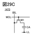
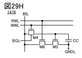
- 29A to 29I are circuit diagrams illustrating a configuration example of a storage device according to one embodiment of the present invention.
- FIG. 30 is a cross-sectional view showing an example of a storage device.
- FIG. 31A is a diagram illustrating an example of a circuit configuration of a memory cell.
- FIG. 31B is a graph showing an example of hysteresis characteristics.
- FIG. 31C is a timing chart showing an example of a method for driving a memory cell.
- FIGS. 32A and 32B are schematic diagrams of a semiconductor device according to one embodiment of the present invention.
- 33A to 33E are diagrams for explaining an example of a storage device.
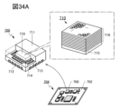
- 34A and 34B are diagrams showing an example of an electronic component.
- 35A and 35B are diagrams showing an example of an electronic device, and
- FIGS. 35C to 35E are diagrams showing an example of a large-sized computer.
- FIG. 36 is a diagram showing an example of space equipment.
- FIG. 37 is a diagram illustrating an example of a storage system applicable to a data center.
- FIG. 38 is a diagram showing the GIXRD measurement results.
- FIGS. 39A and 39B are diagrams showing the results of surface observation using AFM.
- FIGS. 39C and 39D are diagrams showing the results of image analysis.
- FIG. 40A is a diagram showing an input voltage waveform.
- FIG. 40B is a diagram showing P-E characteristics.
- FIG. 41A is a diagram showing an input voltage waveform.
- FIG. 41B is a diagram showing fatigue characteristics.
- FIGS. 42A and 42B are diagrams showing fatigue characteristics.
- FIGS. 43A and 43B are diagrams illustrating a retention measurement method.
- FIG. 44 is a diagram showing the results of retention measurement.
- FIG. 45 is a diagram showing J-V characteristics.
- FIG. 46 is a cross-sectional STEM image of the prepared sample.
- FIG. 47A is a diagram illustrating a memory cell circuit.
- FIG. 47B is an optical micrograph.
- FIGS. 49A and 49B are diagrams illustrating a method of writing and reading evaluation of positive polarization.
- FIGS. 50A and 50B are diagrams illustrating a method of writing and reading evaluation of positive polarization.
- FIG. 51 is a diagram showing voltage waveforms.
- FIG. 52 is a diagram showing changes in ⁇ V BL .
- FIG. 53 is a diagram showing changes in ⁇ V BL .
- FIGS. 54A and 54B are diagrams showing fatigue characteristics.
- FIGS. 55A and 55B are diagrams showing the results of retention measurement.
- FIG. 56A is a schematic diagram of the sample, and FIG. 56B is a cross-sectional view of the sample.
- FIG. 56A is a schematic diagram of the sample
- FIG. 56B is a cross-sectional view of the sample.
- FIG. 57 is a cross-sectional STEM image of the prepared sample.
- FIG. 58 is a diagram showing the Id-Vg characteristics of the sample.
- FIG. 59 is a diagram showing threshold voltages.
- FIG. 60 is a diagram showing the Id-Vg characteristics of the sample.
- FIG. 61A is a diagram showing the threshold voltage of the sample.
- FIG. 61B is a diagram showing the sheet resistance of the sample.
- FIG. 61C is a diagram showing the contact resistance of the sample.
- FIG. 62 is a diagram showing the Id-Vg characteristics of the sample.
- 63A to 63C are diagrams showing the contact resistance of the sample.
- FIG. 64A is a circuit diagram showing the circuit configuration of the sample.
- FIG. 64B is a diagram showing measurement results of leakage current.
- FIG. 64A is a circuit diagram showing the circuit configuration of the sample.
- FIG. 64B is a diagram showing measurement results of leakage current.
- FIG. 65A is a circuit diagram showing the circuit configuration of the sample.
- FIG. 65B is a circuit diagram showing the Id-V CWL characteristics of the sample.
- FIG. 65C is a diagram showing the potential Vsh of the sample.
- FIG. 66A is a diagram showing the results of a sample data retention evaluation test.
- FIG. 66B is a diagram showing the results of a sample data rewriting evaluation test.
- FIG. 67A is a diagram showing contact resistance.
- FIG. 67B is a diagram showing sheet resistance.
- FIG. 68 is a cross-sectional STEM image according to the example.
- FIGS. 69A and 69B are diagrams showing the results of the drain withstand voltage test.
- FIG. 70 is a diagram showing the results of the drain withstand voltage test.
- FIG. 71 is a diagram showing PV characteristics.
- FIG. 72 is a diagram showing fatigue characteristics.
- FIG. 73 is a diagram showing changes in ⁇ V BL .
- ordinal numbers such as “first” and “second” are used for convenience, and do not limit the number of components or the order of the components (for example, the order of steps or the order of lamination). It's not something you do. Further, the ordinal number attached to a constituent element in a certain part of this specification may not match the ordinal number attached to the constituent element in another part of this specification or in the claims.
- film and “layer” can be interchanged depending on the situation or circumstances.
- conductive layer can be changed to the term “conductive film.”
- insulating film can be changed to the term “insulating layer.”
- conductor can be interchanged with the term “conductive layer” or the term “conductive film” depending on the case or the situation.
- insulator can be interchanged with the term “insulating layer” or the term “insulating film” depending on the case or the situation.
- the opening includes, for example, a groove, a slit, etc. Further, a region in which an opening is formed may be referred to as an opening.
- drawings used in this embodiment show a case where the sidewall of the insulator in the opening of the insulator is approximately perpendicular to the substrate surface or the surface to be formed, it may have a tapered shape.
- a tapered shape refers to a shape in which at least a part of the side surface of the structure is inclined with respect to the substrate surface or the surface to be formed.
- a taper angle a region where the angle between the inclined side surface and the substrate surface or the surface to be formed (hereinafter sometimes referred to as a taper angle) is less than 90°.
- the side surfaces of the structure and the substrate surface do not necessarily have to be completely flat, and may be substantially planar with minute curvatures or substantially planar with minute irregularities.
- the heights match refers to a configuration in which the heights from a reference surface (for example, a flat surface such as a substrate surface) are equal in cross-sectional view.
- a reference surface for example, a flat surface such as a substrate surface
- the surface of a single layer or a plurality of layers may be exposed by performing a planarization process (typically a CMP (Chemical Mechanical Polishing) process).
- CMP Chemical Mechanical Polishing
- the surfaces to be subjected to CMP processing have the same height from the reference surface.
- the heights of the plurality of layers may differ depending on the processing apparatus, processing method, or material of the surface to be processed during CMP processing.
- the heights match In this specification, this case is also treated as "the heights match.”
- the height of the top surface of the first layer and the height of the second layer are If the difference from the height of the top surface of the layer is 20 nm or less, it is also said that the heights match.
- the ends coincide means that at least a portion of the outlines of the stacked layers overlap when viewed from above. For example, this includes a case where the upper layer and the lower layer are processed using the same mask pattern or partially the same mask pattern. However, strictly speaking, the contours do not overlap, and the contour of the upper layer may be located inside the contour of the lower layer, or the contour of the upper layer may be located outside the contour of the lower layer. "Concordance”.
- match includes both a complete match and a general match.
- off-state current may refer to, for example, a current flowing between a source and a drain when a transistor is in an off state.
- a configuration example of a semiconductor device that is one embodiment of the present invention will be described with reference to FIGS. 1A to 25B.
- a semiconductor device that is one embodiment of the present invention includes a transistor.
- An insulator 280 is provided on the insulator 222, the conductor 242a, and the conductor 242b.
- the upper surface of insulator 280 may be flattened.
- an insulator 250 and a conductor 260 are provided so as to fill the opening formed in the insulator 280.
- the oxide 230 has a region that functions as a channel formation region.
- the conductor 260 has a region that functions as a first gate electrode (upper gate electrode).
- Insulator 250 has a region that functions as a first gate insulator.
- the conductor 205 has a region that functions as a second gate electrode (lower gate electrode).
- Insulator 222 has a region that functions as a second gate insulator.
- the conductor 242a has a region that functions as either a source electrode or a drain electrode.
- the conductor 242b has a region that functions as the other of a source electrode and a drain electrode.
- the oxide 230 has a region that functions as a channel formation region, in this specification and the like, the oxide 230 can be referred to as a semiconductor layer of the transistor 200A. Further, the semiconductor layer can be referred to as the oxide 230.
- the carrier concentration of the region 230i is 1 ⁇ 10 18 cm ⁇ 3 or less, less than 1 ⁇ 10 17 cm ⁇ 3 , less than 1 ⁇ 10 16 cm ⁇ 3 , less than 1 ⁇ 10 15 cm ⁇ 3 , or 1 ⁇ 10 14 cm -3, less than 1 ⁇ 10 13 cm ⁇ 3 , less than 1 ⁇ 10 12 cm ⁇ 3 , less than 1 ⁇ 10 11 cm ⁇ 3 , or preferably less than 1 ⁇ 10 10 cm ⁇ 3 .
- the lower limit value of the carrier concentration in the region 230i is not particularly limited, but may be set to, for example, 1 ⁇ 10 ⁇ 9 cm ⁇ 3 .
- the oxide 230 may have a single layer structure or a laminated structure.
- the element M includes aluminum, gallium, tin, yttrium, titanium, vanadium, chromium, manganese, iron, cobalt, nickel, zirconium, molybdenum, hafnium, tantalum, tungsten, lanthanum, cerium, neodymium, magnesium, and calcium. , strontium, barium, boron, silicon, germanium, and antimony.
- the element M included in the metal oxide is preferably one or more of the above elements, more preferably one or more selected from aluminum, gallium, tin, and yttrium, and further gallium. preferable. Note that in this specification and the like, metal elements and metalloid elements may be collectively referred to as "metal elements," and the "metal elements" described in this specification and the like may include semimetal elements.
- the field effect mobility of the transistor can be increased.
- the metal oxide may contain one or more metal elements having a large periodic number in the periodic table of elements.
- Metal elements with large period numbers in the periodic table of elements include metal elements belonging to the fifth period, metal elements belonging to the sixth period, and the like.
- the metal oxide becomes highly crystalline, and the diffusion of impurities in the metal oxide can be suppressed. . Therefore, fluctuations in the electrical characteristics of the transistor are suppressed, and reliability can be improved.
- the transistor can obtain a large on-current and high frequency characteristics.
- metal oxides can be used.
- the nearby composition includes a range of ⁇ 30% of the desired atomic ratio.
- the element M it is preferable to use at least one of gallium and aluminum.
- the above atomic ratio is not limited to the atomic ratio of the formed metal oxide, but also the atomic ratio of the sputtering target used for forming the metal oxide film. It may be.
- the channel formation region in the oxide semiconductor preferably has a reduced carrier concentration and is i-type (intrinsic) or substantially i-type.
- the insulator can be converted to an oxide semiconductor. It can supply oxygen and reduce oxygen vacancies and V OH .
- excess oxygen oxygen that is desorbed by heating
- the insulator can be converted to an oxide semiconductor. It can supply oxygen and reduce oxygen vacancies and V OH .
- an excessive amount of oxygen is supplied to the region 230na or the region 230nb, there is a risk that the on-state current of the transistor 200A or the field effect mobility will decrease.
- the amount of oxygen supplied to the region 230na or the region 230nb varies within the substrate plane, resulting in variations in the characteristics of a semiconductor device including a transistor.
- the region 230i has a reduced carrier concentration and is preferably i-type or substantially i-type, whereas the region 230na and the region 230nb have a high carrier concentration and are n-type. is preferred.
- an excessive amount of oxygen is not supplied to the region 230na and the region 230nb, and that the amount of V OH in the region 230na and the region 230nb is not excessively reduced.
- the oxide semiconductor can form V OH , so in order to reduce the amount of V OH , it is necessary to reduce the hydrogen concentration.
- the semiconductor device is configured to supply oxygen to the region 230i and suppress the diffusion of hydrogen to the region 230i. Further, the semiconductor device has a structure in which oxidation of the conductor 242a, the conductor 242b, and the conductor 260 is suppressed. Further, the semiconductor device is configured to reduce the hydrogen concentration in the region 230i.
- the conductor 260 covers the side and top surfaces of the oxide 230.
- the channel formation region can be electrically surrounded by the electric field of the gate electrode.
- a structure of a transistor in which a channel formation region is electrically surrounded by at least the electric field of the first gate electrode is referred to as a surrounded channel (S-channel) structure.
- a laminate of the first insulator on the channel forming region and the second insulator on the first insulator is referred to as a first laminate.
- a laminate of the first insulator under the region 230i and the second insulator under the first insulator is referred to as a second laminate.
- the first stacked body and the second stacked body are provided symmetrically with respect to the channel forming region as a reference or axis.
- the first stacked body and the second stacked body are provided symmetrically with respect to a plane or a line passing through the channel forming region.
- the first stacked body and the second stacked body are provided symmetrically with respect to the channel forming region.
- a configuration in which the first laminate and the second laminate are provided symmetrically with respect to the structure means that the first laminate and the second laminate are arranged symmetrically with respect to the structure.
- the first laminate and the second laminate are provided to sandwich the structure, and in the direction from the first laminate to the second laminate via the structure, Refers to a configuration in which the stacking order of the layers included in the first laminate is opposite to the stacking order of the layers included in the second laminate.
- first laminate, the structure, and the second laminate may be arranged in this order in a direction perpendicular to the substrate surface, or may be arranged in a horizontal direction with respect to the substrate surface.
- first laminate, the structure, and the second laminate are arranged in this order in a direction perpendicular to the substrate surface, the first laminate and the second laminate are It can be said that they are provided above and below the .
- first laminate and the second laminate each have two or more layers. Further, it is preferable that the number of layers included in the first laminate is the same as the number of layers included in the second laminate. Note that one layer included in the first laminate may have the functions of multiple layers included in the second laminate, and vice versa. Further, a structure comprised of a plurality of layers included in the first laminate may have the function of one layer included in the second laminate, and vice versa. Therefore, the number of layers included in the first laminate and the number of layers included in the second laminate may be different. Moreover, the contours of one layer and another layer included in the first laminate do not necessarily have to overlap. The same applies to the second laminate.
- the semiconductor device shown in this embodiment includes a first stacked body, a metal oxide having a channel formation region under the first stacked body, and a second stacked body under the metal oxide.
- the first laminate and the second laminate each include at least a first insulator and a second insulator.
- the first insulator of the first laminate and the first insulator of the second laminate have a region that overlaps with each other via the channel forming region
- the second insulator included in the second stacked body and the second insulator included in the second stacked body are the first insulator included in the first stacked body, the channel forming region, and the first insulator included in the second stacked body. They have regions that overlap each other with an insulator in between.
- the insulator 250 preferably has a laminated structure of an insulator 250a and an insulator 250b on the insulator 250a.
- the insulator 222 preferably has a laminated structure of an insulator 222a and an insulator 222b below the insulator 222a.
- the insulator 250a and the insulator 222a may be provided to sandwich the region 230i of the oxide 230
- the insulator 250b and the insulator 222b may be provided to sandwich the insulator 250a, the region 230i, and the insulator 222a. preferable.
- the insulator 250a and the insulator 222a have a region that overlaps with each other via the region 230i
- the insulator 250b and the insulator 222b have a region that overlaps with each other via the region 230i and the insulator 222a. have areas that overlap with each other.
- an insulator that easily transmits oxygen As the insulator 250a and the insulator 222a, oxygen contained in the insulator 280 can be supplied to the region 230i via the insulator 250a and the insulator 222a. Further, as the insulator 250a and the insulator 222a, an insulator containing excess oxygen may be used. With such a configuration, oxygen contained in the insulator 250a and the insulator 222a can be supplied to the region 230i.
- the concentration of impurities such as water and hydrogen in the insulator 250a and the insulator 222a is reduced.
- the ratio of the permittivity of a medium to the permittivity of a vacuum is called the relative permittivity.
- the relative dielectric constant is the dielectric constant made dimensionless by an electric constant. Therefore, the dielectric constant can be referred to as the relative dielectric constant.
- the concentration of impurities such as water and hydrogen in the insulator 280 is reduced.
- the insulator 280 preferably includes an oxide containing silicon, such as silicon oxide or silicon oxynitride.
- the conductor 260 and the insulator 250 are arranged to fill the opening formed in the insulator 280.
- the conductor 260 is provided in the opening so as to cover at least a portion of the side surface and at least a portion of the top surface of the oxide 230 with the insulator 250 interposed therebetween. Further, the conductor 260 is arranged so that its upper surface is at the same height as the upper surface of the insulator 250 and the upper surface of the insulator 280.
- the side wall of the insulator 280 may be approximately perpendicular to the upper surface of the insulator 222, and may have a tapered shape. It may be. By tapering the sidewall of the insulator 280 in the opening, the coverage of the insulator 250 provided in the opening can be improved and defects such as holes can be reduced.
- the conductor 260 preferably extends in the channel width direction, as shown in FIGS. 1A and 1C. With this structure, the conductor 260 functions as a wiring when a plurality of transistors are provided.
- the conductor 260, the conductor 242a, the conductor 242b, and the conductor 205 it is preferable to use a conductive material that is not easily oxidized or a conductive material that has a function of suppressing oxygen diffusion, respectively.
- the conductive material include a conductive material containing nitrogen and a conductive material containing oxygen.
- the conductor 260, the conductor 242a, the conductor 242b, and the conductor 205 are at least Contains metal and nitrogen.
- the conductor 260 may have a single layer structure or a laminated structure. Further, the conductor 242a and the conductor 242b may have a single layer structure or a laminated structure.
- a conductive material containing nitrogen for example, a nitride containing tantalum, a nitride containing titanium, a nitride containing molybdenum, a nitride containing tungsten, tantalum, and the like. It is preferable to use a nitride containing aluminum, a nitride containing titanium and aluminum, or the like. In one aspect of the invention, nitrides containing tantalum are particularly preferred.
- ruthenium, ruthenium oxide, ruthenium nitride, an oxide containing strontium and ruthenium, an oxide containing lanthanum and nickel, etc. may be used. These materials are preferable because they are conductive materials that are not easily oxidized or materials that maintain conductivity even after absorbing oxygen.
- the conductor 205 is arranged so as to overlap the oxide 230 and the conductor 260. Furthermore, the conductor 205 is preferably provided extending in the channel width direction, as shown in FIGS. 1A and 1C. With this structure, the conductor 205 functions as a wiring when a plurality of transistors are provided.
- the conductor 205 may have a single layer structure or a laminated structure.
- the conductor 205 can function as a second gate electrode.
- the threshold voltage (Vth) of the transistor 200 can be controlled by changing the potential applied to the conductor 205 independently of the potential applied to the conductor 260 without interlocking with the potential applied to the conductor 260.
- the Vth of the transistor 200 can be increased and the off-state current can be decreased. Therefore, when a negative potential is applied to the conductor 205, the drain current when the potential applied to the conductor 260 is 0 V can be made smaller than when no negative potential is applied.
- the potential applied to the conductor 205 may be the same as the potential applied to the conductor 260.
- the electric fields of the conductor 260 and the conductor 205 can be applied to the entire channel formation region of the oxide 230. Therefore, the channel width can be increased without increasing the size of the transistor. Therefore, the on-state current of the transistor can be increased while miniaturizing the transistor. Furthermore, by increasing the on-state current of the transistor, frequency characteristics can be improved.
- FIGS. 1B and 1C show a structure in which a stacked structure of an insulator 222b and an insulator 222a is used as the second gate insulator
- the present invention is not limited to this.
- a stack of the insulator 222 and an island-shaped insulator on the insulator 222 may be used as the second gate insulator.
- an island-shaped insulator may be provided between the insulator 222 and the oxide 230.
- island-like refers to a state in which two or more layers formed in the same process and using the same material are physically separated.
- FIGS. 2A and 2B are cross-sectional views of a semiconductor device including a transistor 200A.
- FIG. 2A is a cross-sectional view of the transistor 200A in the channel length direction
- FIG. 2B is a cross-sectional view of the transistor 200A in the channel width direction.
- FIG. 1A can be referred to for a top view of the semiconductor device shown in FIGS. 2A and 2B.
- the transistor 200A shown in FIGS. 2A and 2B differs from the transistor 200A shown in FIGS. 1B and 1C mainly in that the insulator 222 is a single layer and that the transistor 200A has an island-like insulator 224.
- an island-shaped insulator 224 is provided between the insulator 222 and the oxide 230.
- the side edges of the insulator 224 coincide with the side edges of the oxide 230.
- Each of the insulators 222 and 224 has a region that functions as a second gate insulator.
- the insulator 250a has a region in contact with the top surface of the insulator 222, a region in contact with the side surface of the insulator 224, a region in contact with the side surface of the oxide 230, and a region in contact with the top surface of the oxide 230. At this time, the region 230i of the oxide 230 is surrounded by the insulator 250a and the insulator 224.
- the insulator 222 it is preferable to use a material that can be applied to the above-mentioned insulator 222b. Moreover, it is preferable that the insulator 224 uses a material that can be applied to the above-mentioned insulator 222a. In such a configuration, the laminate consisting of the insulator 222 and the island-shaped insulator 224 can be regarded as a second laminate. At this time, it can be said that the transistor 200A shown in FIGS. 2A and 2B has a configuration in which the first stacked body and the second stacked body are provided symmetrically with respect to the channel formation region.
- FIG. 3A is a top view of the semiconductor device
- FIGS. 3B and 3C are cross-sectional views of the semiconductor device.
- FIG. 3B is a sectional view of a portion indicated by a dashed line A1-A2 in FIG. 3A.
- FIG. 3C is a cross-sectional view of a portion shown by a dashed line A3-A4 in FIG. 3A. Note that in the top view of FIG. 3A, some elements are omitted for clarity.
- FIGS. 3A to 3C includes a transistor 200B. Therefore, FIG. 3B can also be said to be a cross-sectional view of the transistor 200B in the channel length direction. Further, FIG. 3C can also be said to be a cross-sectional view of the transistor 200B in the channel width direction.
- the transistor 200B shown in FIGS. 3B and 3C mainly differs from the transistor 200A shown in FIGS. 1B and 1C in that each of the insulator 222 and the insulator 250 has a three-layer stacked structure.
- the insulator 250 further includes an insulator 250c below the insulator 250a
- the insulator 222 further includes an insulator 222c above the insulator 222a. This is the main difference from the transistor 200A shown in FIGS. 1B and 1C.
- portions that are different from the above-described configuration example 1 will be mainly explained, and descriptions of overlapping portions will be omitted.
- the insulator 250 includes an insulator 250c, an insulator 250a on the insulator 250c, and an insulator 250b on the insulator 250a.
- the insulator 222 includes an insulator 222b, an insulator 222a on the insulator 222b, and an insulator 222c on the insulator 222a.
- the insulator 250c and the insulator 222c have a region that overlaps with each other via the region 230i
- the insulator 250a and the insulator 222a have a region that overlaps with each other via the insulator 250c, the region 230i, and the insulator 222c.
- the insulator 250c and the insulator 222c have barrier properties against oxygen.
- the insulator 250c has a region in contact with the side surface of the conductor 242a and a region in contact with the side surface of the conductor 242b. Since the insulator 250c has barrier properties against oxygen, the side surfaces of the conductor 242a and the conductor 242b can be prevented from being oxidized and formation of an oxide film on the side surfaces. This can suppress the on-state current of the transistor 200B from becoming small or the field-effect mobility from decreasing.
- barrier insulators against oxygen include oxides containing one or both of aluminum and hafnium, oxides containing hafnium and silicon (hafnium silicate), magnesium oxide, gallium oxide, gallium zinc oxide, and indium gallium zinc oxide. , silicon nitride, and silicon nitride oxide.
- oxides containing one or both of aluminum and hafnium include aluminum oxide, hafnium oxide, and oxides containing aluminum and hafnium (hafnium aluminate).
- the insulator 222c is provided between the insulator 222a and the region 230na or the region 230nb. Therefore, diffusion of oxygen from below the insulator 222c to the regions 230na and 230nb can be suppressed. Further, a conductor 242a is provided on the region 230na, and a conductor 242b is provided on the region 230nb. Therefore, in this embodiment, an excessive amount of oxygen is not supplied to the region 230na and the region 230nb.
- insulator 250c and the insulator 222c it is preferable to use an insulator containing an oxide containing one or both of aluminum and hafnium as the insulator 250c and the insulator 222c.
- aluminum oxide is used as the insulator 250c and the insulator 222c.
- each of the insulator 250c and the insulator 222c contains at least oxygen and aluminum.
- the insulator 250c and the insulator 222c have the same function. Therefore, the first stacked body and the second stacked body can be provided symmetrically with respect to the channel formation region.
- the insulator 250c has a region in contact with the top surface of the insulator 222a, a region in contact with the side surface of the insulator 224, a region in contact with the side surface of the oxide 230, and a region in contact with the top surface of the oxide 230. At this time, the region 230i of the oxide 230 is surrounded by the insulator 250c and the insulator 224.
- FIGS. 4A and 4B show a configuration in which an insulator 224 having barrier properties against oxygen is provided between the region 230i and the insulator 222a, the present invention is not limited to this.
- An example of a configuration different from the configuration shown in FIGS. 4A and 4B is shown in FIGS. 5A and 5B.
- the transistor 200B shown in FIGS. 5A and 5B has the following points: the insulator 222 has a two-layer stacked structure, the insulator 224 is not included, and the oxide 230 has a two-layer stacked structure.
- the transistor 200B is mainly different from the transistor 200B shown in FIG.
- the insulator 222 has a stacked structure of an insulator 222b and an insulator 222a on the insulator 222b.
- the oxide 230 has a stacked structure of an oxide 230a and an oxide 230b on the oxide 230a. It is preferable that the oxide 230a be made of a semiconductor material having barrier properties against oxygen, and the oxide 230b be made of a material that can be used for the oxide 230 described above.
- the oxide 230a only needs to be less permeable to oxygen than, for example, the insulator 222a. Further, as the oxide 230a, for example, a material that is less permeable to oxygen than the insulator 222a may be used.
- the laminate made of the insulator 222 and the oxide 230a can be regarded as the second laminate.
- the transistor 200B shown in FIGS. 5A and 5B has a configuration in which the first stacked body and the second stacked body are provided symmetrically with respect to the channel formation region.
- the region 230i, the region 230na, and the region 230nb may be formed not only in the oxide 230b but also in the oxide 230a. be.
- the insulator 222 may have a single layer structure, and an insulator 224 may be provided between the insulator 222 and the oxide 230a.
- the insulator 250c and the oxide 230a have a region that overlaps with each other via the region 230i
- the insulator 250a and the insulator 224 have a region that overlaps with each other via the insulator 250c, the region 230i, and the oxide 230a.
- the insulator 250b and the insulator 222 have an overlapping region with the insulator 250a, the insulator 250c, the region 230i, the oxide 230a, and the insulator 224 interposed therebetween.
- FIGS. 6A to 6C includes a transistor 200C. Therefore, FIG. 6B can also be said to be a cross-sectional view of the transistor 200C in the channel length direction. Further, FIG. 6C can also be said to be a cross-sectional view of the transistor 200C in the channel width direction.
- the transistor 200C shown in FIGS. 6B and 6C mainly differs from the transistor 200A shown in FIGS. 1B and 1C in that each of the insulator 222 and the insulator 250 has a three-layer stacked structure.
- the transistor 200C shown in FIGS. 6B and 6C includes an insulator 250d between an insulator 250a and an insulator 250b, and an insulator 222d between an insulator 222a and an insulator 222b. This is the main difference from the transistor 200A shown in FIGS. 1B and 1C.
- portions that are different from the above-described configuration example 1 will be mainly explained, and descriptions of overlapping portions will be omitted.
- the insulator 250d and the insulator 222d have a function of capturing or fixing hydrogen.
- hydrogen inside the region can be captured or fixed more effectively. be able to.
- hydrogen contained in the insulator 250a, the region 230i of the oxide 230b, and the insulator 222a can be captured or fixed more effectively. Therefore, the hydrogen concentration in the region 230i can be reduced. Therefore, the V O H in region 230i can be reduced, making region 230i i-type or substantially i-type.
- Examples of insulators that have the function of capturing or fixing hydrogen include metal oxides with an amorphous structure.
- metal oxides with an amorphous structure As the insulator 250d and the insulator 222d, it is preferable to use, for example, a metal oxide such as magnesium oxide or an oxide containing one or both of aluminum and hafnium.
- metal oxides having such an amorphous structure oxygen atoms have dangling bonds, and the dangling bonds may capture or fix hydrogen.
- metal oxides having an amorphous structure have a high ability to capture or fix hydrogen.
- a material with a high dielectric constant (high-k) for the insulator 250d and the insulator 222d.
- high-k materials include oxides containing one or both of aluminum and hafnium, tantalum oxide, zirconium oxide, hafnium zirconium oxide, and the like.
- problems such as leakage current may occur due to thinning of gate insulators.
- a high-k material as the insulator 250d and the insulator 222d, it is possible to reduce the gate potential applied during transistor operation while maintaining the physical thickness of the gate insulator.
- EOT equivalent oxide thickness
- a substance with a high dielectric constant such as lead zirconate titanate (PZT), strontium titanate (SrTiO 3 ), (Ba,Sr)TiO 3 (BST) can be used. In some cases.
- hafnium oxide is used as the insulator 250d and the insulator 222d.
- each of the insulator 250d and the insulator 222d contains at least oxygen and hafnium.
- the hafnium oxide has an amorphous structure.
- the insulator 250d and the insulator 222d have an amorphous structure.
- the insulator 250d and the insulator 222d have the same function. Therefore, the first stacked body and the second stacked body can be provided symmetrically with respect to the channel formation region.
- the second gate insulator may be composed of a stacked body of an insulator 222 and an island-shaped insulator 224.
- FIGS. 7A and 7B are cross-sectional views of a semiconductor device including a transistor 200C.
- FIG. 7A is a cross-sectional view of the transistor 200C in the channel length direction
- FIG. 7B is a cross-sectional view of the transistor 200C in the channel width direction. Note that FIG. 6A can be referred to for a top view of the semiconductor device shown in FIGS. 7A and 7B.
- the insulator 250a has a region in contact with the top surface of the insulator 222d, a region in contact with the side surface of the insulator 224, a region in contact with the side surface of the oxide 230, and a region in contact with the top surface of the oxide 230. At this time, the region 230i of the oxide 230 is surrounded by the insulator 250a and the insulator 224.
- the insulator 224 is preferably made of a material that can be used for the insulator 222a described above.
- FIGS. 7C and 7D are cross-sectional views of a semiconductor device including a transistor 200C.
- FIG. 7C is a cross-sectional view of the transistor 200C in the channel length direction
- FIG. 7D is a cross-sectional view of the transistor 200C in the channel width direction.
- FIG. 6A can be referred to for a top view of the semiconductor device shown in FIGS. 7C and 7D.
- FIGS. 8A to 8C Configuration examples different from the above-described transistors 200A to 200C are shown in FIGS. 8A to 8C.
- FIG. 8A is a top view of the semiconductor device
- FIGS. 8B and 8C are cross-sectional views of the semiconductor device.
- FIG. 8B is a sectional view of a portion shown by a dashed line A1-A2 in FIG. 8A.
- FIG. 8C is a cross-sectional view of the portion shown by the dashed line A3-A4 in FIG. 8A. Note that in the top view of FIG. 8A, some elements are omitted for clarity.
- the body 222b includes an insulator 250d, an insulator 250a, an insulator 250c, a region 230i, an insulator 222c, an insulator 222a, and a region that overlaps each other via an insulator 222d.
- the transistor 200D shown in FIGS. 9A and 9B, the transistor 200D shown in FIGS. 9C and 9D, and the transistor 200D shown in FIGS. 9E and 9F have an island-shaped insulator 224 between the insulator 222 and the oxide 230. This is the main difference from the transistor 200D shown in FIGS. 8B and 8C.
- the insulator 222 has a single-layer structure, and the insulator 224 includes an insulator 224d, an insulator 224a on the insulator 224d, and an insulator 224a on the insulator 224a. It has a laminated structure with 224c.
- the insulator 222 it is preferable to use a material that can be used for the above-mentioned insulator 222b.
- the insulator 224d is made of a material applicable to the above-mentioned insulator 222d
- the insulator 224a is made of a material applicable to the above-described insulator 222a
- the insulator 224c is made of a material applicable to the above-described insulator 222c. It is preferable to use
- the laminate consisting of the insulator 222 and the insulator 224 can be regarded as a second laminate.
- the first stacked body and the second stacked body have a channel It can be said that the configuration is symmetrical with respect to the formation area.
- the transistor 200D shown in FIGS. 10A and 10B differs from the transistor 200D shown in FIGS. 8B and 8C mainly in that the oxide 230 has a two-layer stacked structure.
- the transistor 200D shown in FIGS. 10C and 10D and the transistor 200D shown in FIGS. 10E and 10F have the island-shaped insulator 224 and the oxide 230 has a two-layer stacked structure. This is mainly different from the transistor 200D shown in 8C.
- the insulator 224 includes an insulator 224d and an insulator 224a on the insulator 224d.
- the oxide 230 has a stacked structure of an oxide 230a and an oxide 230b on the oxide 230a.
- the insulator 222 it is preferable to use a material that can be used for the above-mentioned insulator 222b.
- the insulator 224d uses a material that can be used for the above-described insulator 222d
- the insulator 224a uses a material that can be used for the above-described insulator 222a.
- the laminate consisting of the insulator 222, the insulator 224, and the oxide 230a can be regarded as a second laminate.
- the first stacked body and the second stacked body are provided symmetrically with respect to the channel formation region. It can be said that it has a structure.
- FIGS. 11A and 11B, FIG. 11C and FIG. 11D, FIG. 12A and FIG. 12B, and FIG. 12C and FIG. 12D are respectively cross-sectional views of a semiconductor device having a transistor 200D.
- FIGS. 11A, 11C, 12A, and 12C are cross-sectional views of the transistor 200D in the channel length direction
- FIGS. 11B, 11D, 12B, and 12D are cross-sectional views of the transistor 200D in the channel width direction. It is.
- the top view of the semiconductor device shown in FIGS. 11A and 11B and the semiconductor device shown in FIGS. 11C and 11D can be seen in FIG. 3A, and the top view of the semiconductor device shown in FIGS.
- FIG. 8A For a top view of the illustrated semiconductor device, see FIG. 8A.
- the transistor 200D shown in FIGS. 11A and 11B and the transistor 200D shown in FIGS. 11C and 11D have an insulator 222d and do not have an insulator 250d.
- the transistor 200D shown in FIGS. 11A and 11B differs from the transistor 200B shown in FIGS. 4C and 4D in that it includes an insulator 222d. Further, the transistor 200D shown in FIGS. 11A and 11B differs from the transistor 200D shown in FIGS. 9C and 9D in that it does not include an insulator 250d. Therefore, the transistor 200D shown in FIGS. 11A and 11B can be said to be a modification of the transistor 200B shown in FIGS. 4C and 4D, or a modification of the transistor 200D shown in FIGS. 9C and 9D.
- the transistor 200D shown in FIGS. 11C and 11D differs from the transistor 200B shown in FIGS. 5C and 5D in that an insulator 222d is provided between the insulator 222b and the insulator 224. Further, the transistor 200D shown in FIGS. 11C and 11C differs from the transistor 200D shown in FIGS. 10C and 10D in that it does not include an insulator 250d. Therefore, the transistor 200D shown in FIGS. 11C and 11D can be said to be a modification of the transistor 200B shown in FIGS. 5C and 5D, or a modification of the transistor 200D shown in FIGS. 10C and 10D. Further, the transistor 200D shown in FIGS. 10C and 10D has a structure in which an insulator 250d is provided between an insulator 250a and an insulator 250b in the transistor 200D shown in FIGS. 11C and 11D.
- the transistor 200D shown in FIGS. 12A and 12B and the transistor 200D shown in FIGS. 12C and 12D have an insulator 250d and do not have an insulator 222d.
- the transistor 200D shown in FIGS. 12A and 12B differs from the transistor 200B shown in FIGS. 4C and 4D in that it includes an insulator 250d. Furthermore, the transistor 200D shown in FIGS. 12A and 12B differs from the transistor 200D shown in FIGS. 9C and 9D in that it does not include an insulator 222d. Therefore, the transistor 200D shown in FIGS. 12A and 12B can be said to be a modification of the transistor 200B shown in FIGS. 4C and 4D, or a modification of the transistor 200D shown in FIGS. 9C and 9D.
- the transistor 200D shown in FIGS. 12C and 12D differs from the transistor 200B shown in FIGS. 5C and 5D in that it includes an insulator 250d.
- the transistor 200D shown in FIGS. 12C and 12D has a structure in which an insulator 250d is added to the transistor 200B shown in FIGS. 5C and 5D.
- the transistor 200D shown in FIGS. 12C and 12D differs from the transistor 200D shown in FIGS. 10C and 10D in that it does not include an insulator 222d. Therefore, the transistor 200D shown in FIGS. 12C and 12D can be said to be a modification of the transistor 200B shown in FIGS. 5C and 5D, or a modification of the transistor 200D shown in FIGS. 10C and 10D.
- the insulator 222 of the transistor 200D shown in FIGS. 12A and 12B and the transistor 200D shown in FIGS. 12C and 12D may be made of a material applicable to the insulator 222b described above, or may be made of a material applicable to the insulator 222d described above. Any applicable material may be used.
- the insulator 222 When using a material applicable to the insulator 222d described above as the insulator 222 of the transistor 200D shown in FIGS. 12A and 12B and the transistor 200D shown in FIGS. It is preferable to have a function of suppressing the diffusion of at least one of atoms and hydrogen molecules.
- the insulator 222 preferably has a function of suppressing hydrogen diffusion more than the insulator 224 (the insulator 224a in the transistor 200D shown in FIGS. 12A and 12B).
- the insulator 222 may have a function of suppressing the diffusion of oxygen (for example, at least one of oxygen atoms and oxygen molecules).
- the insulator 222 preferably has a function of suppressing oxygen diffusion more than the insulator 224 (the insulator 224a in the transistor 200D shown in FIGS. 12A and 12B).
- the insulator 222 may be formed using an oxide of one or both of aluminum and hafnium, or an oxide containing hafnium and zirconium. preferable.
- the insulator 222 suppresses the diffusion of impurities such as hydrogen from the substrate side to the oxide 230, and suppresses the release of oxygen from the oxide 230 to the substrate side. Acts as a layer. Therefore, impurities such as hydrogen can be suppressed from diffusing inside the transistor 200D, and generation of oxygen vacancies in the oxide 230 can be suppressed. Further, it is possible to suppress the conductor 205 from reacting with oxygen included in the oxide 230.
- aluminum oxide, bismuth oxide, germanium oxide, niobium oxide, silicon oxide, titanium oxide, tungsten oxide, yttrium oxide, or zirconium oxide may be added to the above insulator.
- these insulators may be nitrided.
- the thickness of the insulator 222 is preferably larger than the thickness of the insulator 250d, and more preferably larger than the sum of the thicknesses of the insulator 250d and the insulator 250b.
- the insulator 222 has a function of capturing or fixing hydrogen, and a function of suppressing diffusion of hydrogen (for example, at least one of hydrogen atoms and hydrogen molecules). It may have.
- the insulator 222 can have both the function of the material applicable to the above-mentioned insulator 222b and the function of the material applicable to the above-described insulator 222d.
- the first stacked body and the second stacked body are aligned with respect to the channel formation region. It can be said that it has a symmetrical configuration.
- an insulator having barrier properties against hydrogen may be provided above the first gate electrode and/or below the second gate electrode.
- FIG. 13A and 13B, FIG. 13C and FIG. 13D, and FIG. 13E and FIG. 13F are respectively cross-sectional views of a semiconductor device having a transistor 200E.
- FIGS. 13A, 13C, and 13E are cross-sectional views of the transistor 200E in the channel length direction
- FIGS. 13B, 13D, and 13F are cross-sectional views of the transistor 200E in the channel width direction.
- FIG. 1A can be referred to for top views of the semiconductor devices shown in FIGS. 13A and 13B, the semiconductor devices shown in FIGS. 13C and 13D, and the semiconductor devices shown in FIGS. 13E and 13F.
- parts that are different from the above-mentioned configuration examples 1 to 4 will be mainly explained, and descriptions of overlapping parts will be omitted.
- an insulator 283 is provided above the conductor 260. Further, in the transistor 200E shown in FIGS. 13C and 13D, an insulator 215 is provided below the conductor 205. Further, in the transistor 200E shown in FIGS. 13E and 13F, an insulator 283 is provided above the conductor 260, and an insulator 215 is provided below the conductor 205.
- the insulator 283 preferably has barrier properties against hydrogen.
- the insulator 283 it is possible to suppress impurities such as hydrogen contained in the structure provided above the insulator 283 from diffusing into the region 230i.
- the insulator 215 has hydrogen barrier properties like the insulator 222b.
- the insulator 215 it is possible to suppress impurities such as hydrogen contained in the structure provided below the insulator 215 from diffusing into the region 230i.
- the insulator 216 is provided over the insulator 215, and the conductor 205 is arranged so as to fill the opening formed in the insulator 216. Furthermore, the top surface of the conductor 205 and the top surface of the insulator 216 match in height.
- the electrical resistivity of the conductor 205 is designed in consideration of the potential applied to the conductor 205, and the film thickness of the conductor 205 is set according to the electrical resistivity. Furthermore, the thickness of the insulator 216 is approximately the same as that of the conductor 205. Here, it is preferable that the film thicknesses of the conductor 205 and the insulator 216 be made as thin as the design of the conductor 205 allows. By reducing the thickness of the insulator 216, the absolute amount of impurities such as hydrogen contained in the insulator 216 can be reduced, so that diffusion of the impurities into the oxide 230 can be suppressed.
- the insulator 216 has a lower dielectric constant than the insulator 215.
- an insulator that can be used as the insulator 280 may be used as the insulator 216.
- the diffusion of hydrogen from above the transistor 200 to the region 230i can be sufficiently suppressed by providing the insulator 283 having the same function as the insulator 250b, a structure in which the insulator 250b is not provided may be used. Further, if the diffusion of hydrogen from below the transistor 200 to the region 230i can be sufficiently suppressed by providing the insulator 215 having the same function as the insulator 222b, a structure in which the insulator 222b is not provided may be used.
- FIG. 14A and 14B, FIG. 14C and FIG. 14D, and FIG. 14E and FIG. 14F are cross-sectional views of a semiconductor device having a transistor 200E.
- FIGS. 14A, 14C, and 14E are cross-sectional views of the transistor 200E in the channel length direction
- FIGS. 14B, 14D, and 14F are cross-sectional views of the transistor 200E in the channel width direction.
- FIG. 8A can be referred to for top views of the semiconductor devices shown in FIGS. 14A and 14B and the semiconductor devices shown in FIGS. 14C and 14D.
- FIG. 3A For a top view of the semiconductor device shown in FIGS. 14E and 14F, refer to FIG. 3A.
- the transistor 200E shown in FIGS. 14A and 14B differs from the transistor 200D shown in FIGS. 9C and 9D in that an insulator 215 is provided and an insulator 222b is not provided. Unlike the transistor 200D shown in FIG. 10D, the transistor 200E shown in FIGS. 14E and 14F is different from the transistor 200E shown in FIGS. 11C and 11D.
- an insulator having the function of capturing or fixing hydrogen can be provided between the conductor 205 and the insulator 216 and the oxide 230. , an increase in hydrogen concentration in the region 230i can be suppressed.
- FIG. 15A is a top view of a semiconductor device having a transistor 200
- FIGS. 15B to 15D are cross-sectional views of the semiconductor device.
- FIG. 15B is a cross-sectional view of a portion indicated by a dashed line A1-A2 in FIG. 15A, and is also a cross-sectional view of the transistor 200 in the channel length direction.
- FIG. 15C is a cross-sectional view of a portion indicated by a dashed line A3-A4 in FIG. 15A, and is also a cross-sectional view of the transistor 200 in the channel width direction.
- FIG. 15D is a cross-sectional view of a portion indicated by a dashed line A5-A6 in FIG.
- FIG. 15A is also a cross-sectional view of the transistor 200 in the channel width direction. Note that in the top view of FIG. 15A, some elements are omitted for clarity. Further, hereinafter, parts that are different from those described above will be mainly explained, and descriptions of overlapping parts will be omitted.
- the transistor 200 includes an insulator 216 over an insulator 215, a conductor 205 (a conductor 205a and a conductor 205b) embedded in the insulator 216, and an insulator over the insulator 216 and the conductor 205.
- An insulator 275 is provided on the insulator 271a and the insulator 271b, and an insulator 280 is provided on the insulator 275.
- the insulator 250 and the conductor 260 are embedded in the openings formed in the insulator 280 and the insulator 275.
- an insulator 282 is provided over the insulator 280, the conductor 260, and the insulator 250.
- an insulator 283 is provided on the insulator 282.
- the insulator 224, the oxide 230, the conductor 242a, and the conductor 242b have shapes in which the side end portions of the insulator 224, the oxide 230, the conductor 242a, and the conductor 242b match each other as described above.
- any one of the transistors 200A to 200E described above may be applied to the transistor 200 shown in FIGS. 15A to 15D.
- FIGS. 17A and 17B show an example in which the configuration of the transistor 200E shown in FIGS. 14C and 14D is applied to the transistor 200 shown in FIGS. 15A to 15D.
- 17A is an enlarged cross-sectional view of the transistor 200 in the channel length direction
- FIG. 17B is an enlarged cross-sectional view of the transistor 200 in the channel width direction.
- the oxide 230 preferably includes an oxide 230a on the insulator 224 and an oxide 230b on the oxide 230a.
- oxide semiconductor having crystallinity it is preferable to use an oxide semiconductor having crystallinity as the oxide 230b.
- oxide semiconductors having crystallinity include CAAC-OS (c-axis aligned crystalline oxide semiconductor), nc-OS (nanocrystalline oxide semiconductor), and polycrystalline oxide semiconductors. Examples include semiconductors, single crystal oxide semiconductors, and the like.
- CAAC-OS c-axis aligned crystalline oxide semiconductor
- nc-OS nanocrystalline oxide semiconductor
- polycrystalline oxide semiconductors examples include semiconductors, single crystal oxide semiconductors, and the like.
- CAAC-OS c-axis aligned crystalline oxide semiconductor
- nc-OS nanocrystalline oxide semiconductor
- polycrystalline oxide semiconductors examples include semiconductors, single crystal oxide semiconductors, and the like.
- CAAC-OS c-axis aligned crystalline oxide semiconductor
- nc-OS nanocrystalline oxide semiconductor
- polycrystalline oxide semiconductors examples include semiconductors, single crystal oxide semiconductors, and the like.
- CAAC-OS c-axi
- CAAC-OS is a metal oxide that has a highly crystalline and dense structure and has few impurities and defects (for example, oxygen vacancies).
- heat treatment at a temperature that does not polycrystallize the metal oxide (e.g., 400°C or higher and 600°C or lower) allows CAAC-OS to have a more highly crystalline and dense structure. It can be done. In this way, by further increasing the density of the CAAC-OS, it is possible to further reduce diffusion of impurities or oxygen in the CAAC-OS.
- CAAC-OS it is difficult to confirm clear grain boundaries, so it can be said that reduction in electron mobility due to grain boundaries is less likely to occur. Therefore, the metal oxide with CAAC-OS has stable physical properties. Therefore, metal oxides with CAAC-OS are resistant to heat and have high reliability.
- the oxide 230b Furthermore, by using a crystalline oxide such as CAAC-OS as the oxide 230b, it is possible to suppress the extraction of oxygen from the oxide 230b by the conductor 242a or the conductor 242b. As a result, even if heat treatment is performed, oxygen can be suppressed from being extracted from the oxide 230b, so that the transistor 200 is stable against high temperatures (so-called thermal budget) during the manufacturing process. Further, it is possible to suppress a decrease in the conductivity of the conductor 242a and the conductor 242b.
- a crystalline oxide such as CAAC-OS
- oxide semiconductors have various structures, each of which has different characteristics.
- the oxide 230b is a CAAC-OS, a nc-OS, an amorphous-like oxide semiconductor (a-like OS), an amorphous oxide semiconductor, a polycrystalline oxide semiconductor, a CAC-OS ( cloud-aligned composite oxide semiconductor).
- the position of the peak (2 ⁇ value) indicating c-axis orientation may vary depending on the type, composition, etc. of the metal element constituting the CAAC-OS.
- a plurality of bright points (spots) are observed in the electron diffraction pattern of the CAAC-OS film. Note that a certain spot and another spot are observed at positions that are symmetrical with respect to the spot of the incident electron beam that has passed through the sample (also referred to as a direct spot) as the center of symmetry.
- electron beam diffraction also called nanobeam electron diffraction
- an electron beam with a probe diameter equal to or smaller than the nanocrystal for example, from 1 nm to 30 nm
- An electron diffraction pattern in which a plurality of spots are observed within a ring-shaped region centered on the spot may be obtained.
- the oxide 230b has a region 230bi, and a region 230bna and a region 230bnb that are provided to sandwich the region 230bi. Note that for the region 230bi, the region 230bna, and the region 230bnb, the descriptions of the region 230i, the region 230na, and the region 230nb described above can be referred to, respectively.
- the insulator 250 may have a laminated structure of an insulator 250c in contact with the oxide 230, an insulator 250a on the insulator 250c, and an insulator 250b on the insulator 250a.
- the insulator 250 includes an insulator 250c in contact with the oxide 230, an insulator 250a on the insulator 250c, an insulator 250d on the insulator 250a, and an insulator 250d. It is preferable to have a laminated structure including the upper insulator 250b.
- the insulators 250a to 250d are provided inside an opening formed in an insulator 280 or the like together with the conductor 260. In order to miniaturize the transistor 200, it is preferable that each of the insulators 250a to 250d be thin.
- the thickness of each of the insulators 250a to 250d is preferably 0.1 nm or more and 10 nm or less, more preferably 0.1 nm or more and 5.0 nm or less, more preferably 0.5 nm or more and 5.0 nm or less, and 1.0 nm or more. It is more preferably 1.0 nm or more and less than 3.0 nm, and even more preferably 1.0 nm or more and 3.0 nm or less. Note that each of the insulators 250a to 250d only needs to have a region with the thickness described above in at least a portion thereof.
- the ALD method can deposit atoms one layer at a time, it is possible to form extremely thin films, to form structures with high aspect ratios, to form films with few defects such as pinholes, and to improve coverage. It has the advantage of being able to form excellent films and being able to form films at low temperatures. Therefore, the insulator 250 can be formed with a thin film thickness as described above with good coverage on the side surfaces of the openings formed in the insulator 280 and the insulator 275, and the side edges of the conductor 242a and the conductor 242b. It can be membraned.
- a film formed by the ALD method may contain more impurities such as carbon than a film formed by other film forming methods.
- the impurities can be quantified using secondary ion mass spectrometry (SIMS), X-ray photoelectron spectroscopy (XPS), or Auger electron spectroscopy (AES). ger Electron Spectroscopy) It can be done using
- the insulator 250 can be configured to include at least one of insulators 250a to 250d. By forming the insulator 250 with one layer, two layers, or three layers among the insulators 250a to 250d, the manufacturing process of the semiconductor device can be simplified and productivity can be improved.
- the insulator 222b it is preferable to use, for example, silicon nitride formed by an ALD method (particularly a PEALD method).
- ALD method to form the insulator 222b, even if unevenness is formed between the insulator 216 and the conductor 205, the insulator 222b can be formed with good coverage. Therefore, formation of pinholes or breaks in the insulator 222d formed on the insulator 222b can be suppressed.
- the insulator 222 has a single layer structure. Note that similarly to the transistor 200D shown in FIGS. 12A and 12B and the transistor 200D shown in FIGS. 12C and 12D, the insulator 222 with a large thickness can be formed using a material that can be applied to the insulator 222b described above. preferable.
- the insulator 222 has a single-layer structure or a two-layer structure of the insulator 222b and the insulator 222d in the above description, the present invention is not limited to this.
- the insulator 222 may have a laminated structure of three or more layers.
- the insulator 224 is preferably processed into an island shape.
- insulators 224 of approximately the same size are provided for one transistor 200.
- the amount of oxygen supplied from the insulator 224 to the oxide 230 becomes approximately the same. Therefore, variations in the electrical characteristics of the transistor 200 within the plane of the substrate can be suppressed.
- the insulator 224 may have a laminated structure of two or more layers. In that case, the structure is not limited to a laminated structure made of the same material, but may be a laminated structure made of different materials. Alternatively, as shown in FIG. 1B or the like, a configuration in which the insulator 224 is not provided may be used.
- the insulator 275 preferably has barrier properties against oxygen.
- the insulator 275 is provided between the insulator 280 and the conductor 242a and between the insulator 280 and the conductor 242b.
- oxygen contained in the insulator 280 can be suppressed from diffusing into the conductor 242a and the conductor 242b. Therefore, it is possible to prevent the conductor 242a and the conductor 242b from being oxidized by the oxygen contained in the insulator 280, increasing the resistivity, and reducing the on-current.
- the insulator 275 is at least less permeable to oxygen than the insulator 280.
- insulator 275 includes at least nitrogen and silicon.
- the insulator 275 is provided between the insulator 280 and the region 230bna and between the insulator 280 and the region 230bnb.
- the region 230bna and the region 230bnb are surrounded by the insulator 275 and the oxide 230a. Therefore, oxygen contained in the insulator 280 can be suppressed from diffusing into the region 230bna and the region 230bnb.
- barrier insulators against hydrogen examples include oxides such as aluminum oxide, hafnium oxide, and tantalum oxide, and nitrides such as silicon nitride.
- oxides such as aluminum oxide, hafnium oxide, and tantalum oxide
- nitrides such as silicon nitride.
- the insulator 275 has a single layer structure or a multilayer structure of the hydrogen barrier insulator.
- the present invention is not limited to this.
- the insulator 271a and the insulator 271b may each have a laminated structure.
- One or both of the insulator 282 and the insulator 283 functions as a barrier insulator that suppresses impurities such as water and hydrogen from diffusing into the transistor 200 and the like from the substrate side or from above the transistor 200 and the like. is preferred. Therefore, one or both of the insulator 282 and the insulator 283 may contain impurities such as hydrogen atoms, hydrogen molecules, water molecules, nitrogen atoms, nitrogen molecules, nitrogen oxide molecules ( N2O , NO, NO2, etc.), copper atoms, etc. It is preferable to use an insulating material that has a function of suppressing the diffusion of (the above-mentioned impurities are difficult to pass through). Alternatively, it is preferable to have an insulating material that has a function of suppressing the diffusion of oxygen (for example, at least one of oxygen atoms and oxygen molecules) (the above-mentioned oxygen is difficult to permeate).
- the insulator 282 and the insulator 283 each have an insulator having a function of suppressing the diffusion of impurities such as water and hydrogen, and oxygen, and for example, aluminum oxide, magnesium oxide, hafnium oxide, gallium oxide, Indium gallium zinc oxide, silicon nitride, silicon nitride oxide, or the like can be used.
- the insulator 283 it is preferable to use silicon nitride, which has a higher hydrogen barrier property.
- the insulator 282 preferably includes aluminum oxide, magnesium oxide, or the like, each of which has a high ability to capture or fix hydrogen.
- the conductor 205a has a function of suppressing the diffusion of impurities such as hydrogen atoms, hydrogen molecules, water molecules, nitrogen atoms, nitrogen molecules, nitrogen oxide molecules ( N2O , NO, NO2 , etc.), and copper atoms.
- the conductive material has a conductive material having the following properties.
- the conductor 205a By using a conductive material that has a function of reducing hydrogen diffusion for the conductor 205a, it is possible to prevent impurities such as hydrogen contained in the conductor 205b from diffusing into the oxide 230 via the insulator 216 or the like. It can be prevented. In addition, by using a conductive material that has a function of suppressing oxygen diffusion for the conductor 205a, it is possible to prevent the conductor 205b from being oxidized and the conductivity from decreasing. Examples of the conductive material having the function of suppressing oxygen diffusion include titanium, titanium nitride, tantalum, tantalum nitride, ruthenium, and ruthenium oxide.
- the conductor 205a can have a single layer structure or a laminated structure of the above-mentioned conductive materials.
- the conductor 205a preferably includes titanium nitride.
- the conductor 205b preferably includes tungsten.
- the conductor 242a and the conductor 242b each have a region in contact with the oxide 230b.
- the conductor 242a and the conductor 242b may have a single layer structure or a laminated structure.
- each of the conductor 242a and the conductor 242b may have a two-layer structure.
- the conductor 242a is a laminate of a conductor 242a1 and a conductor 242a2 on the conductor 242a1
- the conductor 242b is a laminate of a conductor 242b1 and a conductor 242b2 on the conductor 242b1.
- the above-described conductive material that is not easily oxidized or a conductive material that has a function of suppressing oxygen diffusion as the layer (conductor 242a1 and conductor 242b1) in contact with the oxide 230b. This can prevent the conductor 242a and the conductor 242b from being excessively oxidized by oxygen contained in the oxide 230b. Further, it is possible to suppress a decrease in the conductivity of the conductor 242a and the conductor 242b.
- the conductor 242a2 and the conductor 242b2 have higher conductivity than the conductor 242a1 and the conductor 242b1.
- the thickness of the conductor 242a2 and the conductor 242b2 be larger than the thickness of the conductor 242a1 and the conductor 242b1.
- a conductor that can be used as the conductor 205b may be used. With the above structure, the resistance of the conductor 242a2 and the conductor 242b2 can be reduced. Thereby, the conductor 242a and the conductor 242b can function as highly conductive wiring or electrodes. Further, the operating speed of the transistor 200 can be improved.
- tantalum nitride or titanium nitride can be used as the conductor 242a1 and the conductor 242b1, and tungsten can be used as the conductor 242a2 and the conductor 242b2.
- the conductor 260 is arranged so as to fill the openings formed in the insulator 280 and the insulator 275, as shown in FIGS. 16A to 17B.
- the conductor 260 is provided in the opening so as to cover the side surface of the insulator 224, the side surface of the oxide 230a, and the side surface and top surface of the oxide 230b via the insulator 250.
- a curved surface may be provided between the side surface of the oxide 230b and the top surface of the oxide 230b. That is, the end of the side surface and the end of the top surface may be curved (hereinafter also referred to as round shape). With such a shape, the coverage of the oxide 230b with the insulator 250 and the conductor 260 can be improved.
- the island-shaped insulator 224 In the configuration in which the island-shaped insulator 224 is provided, at least a portion of the lower surface of the conductor 260 can be provided below the lower surface of the oxide 230b, as shown in FIGS. 16B and 17B. Accordingly, the conductor 260 can be provided opposite the top surface and side surfaces of the oxide 230b, so that the electric field of the conductor 260 can be applied to the top surface and side surfaces of the oxide 230b.
- the S-channel structure disclosed in this specification and the like has a structure different from the Fin type structure and the planar type structure.
- the S-channel structure disclosed in this specification and the like can also be regarded as a type of Fin type structure.
- a Fin type structure refers to a structure in which a gate electrode is arranged so as to surround at least two or more surfaces (specifically, two, three, or four sides) of a channel.
- the channel formation region can be electrically surrounded.
- the S-channel structure is a structure that electrically surrounds the channel formation region, it is substantially equivalent to a GAA (Gate All Around) structure or an LGAA (Lateral Gate All Around) structure. You can say that.
- the transistor 200 illustrated in FIGS. 16B and 17B has an S-channel structure
- the semiconductor device of one embodiment of the present invention is not limited thereto.
- the transistor structure that can be used in one embodiment of the present invention may be one or more selected from a planar structure, a fin structure, and a GAA structure.
- the conductor 260 is shown in a two-layer structure.
- the conductor 260 preferably includes a conductor 260a and a conductor 260b disposed on the conductor 260a.
- the conductor 260a is arranged so as to cover the bottom and side surfaces of the conductor 260b.
- the conductor 260a it is preferable to use a conductive material that has a function of suppressing the diffusion of impurities such as hydrogen atoms, hydrogen molecules, water molecules, nitrogen atoms, nitrogen molecules, nitrogen oxide molecules, and copper atoms.
- impurities such as hydrogen atoms, hydrogen molecules, water molecules, nitrogen atoms, nitrogen molecules, nitrogen oxide molecules, and copper atoms.
- a conductive material that has a function of suppressing the diffusion of oxygen for example, at least one of oxygen atoms and oxygen molecules).
- the conductor 260a has a function of suppressing oxygen diffusion, it is possible to suppress the conductor 260b from being oxidized by oxygen contained in the insulator 280 and the like, and thereby reducing its conductivity.
- the conductive material having the function of suppressing oxygen diffusion it is preferable to use, for example, titanium, titanium nitride, tantalum, tantalum nitride, ruthenium, ruthenium oxide, or the like.
- the conductor 260b can be made of a conductive material containing tungsten, copper, or aluminum as a main component.
- the conductor 260b may have a laminated structure, for example, a laminated structure of titanium or titanium nitride and the above conductive material.
- the conductor 260 is formed in a self-aligned manner so as to fill an opening formed in the insulator 280 or the like.
- the conductor 260 can be reliably placed in the region between the conductor 242a and the conductor 242b without alignment.
- FIG. 16A shows a configuration in which the insulator 250c is in contact with the side surfaces of the conductor 242a2 and the conductor 242b2, the present invention is not limited to this.
- an insulator 255 may be provided between the insulator 250c and the conductor 242a2 and between the insulator 250c and the conductor 242b2.
- FIG. 18A and 18B are enlarged cross-sectional views of the transistor 200 in the channel length direction.
- the semiconductor device shown in FIG. 18A and the semiconductor device shown in FIG. 18B are modifications of the semiconductor device shown in FIG. 16A.
- the semiconductor device shown in FIG. 18A and the semiconductor device shown in FIG. 18B have an insulator 255 between the insulator 250c and the conductor 242a2 and between the insulator 250c and the conductor 242b2. , which is different from the semiconductor device shown in FIG. 16A.
- the distance between the conductor 242a1 and the conductor 242b1 is smaller than the distance between the conductor 242a2 and the conductor 242b2.
- the insulator 255 is preferably an insulator that is not easily oxidized, such as nitride.
- the insulator 255 is formed in contact with the side surface of the conductor 242a2 and the side surface of the conductor 242b2, and has a function of protecting the conductor 242a2 and the conductor 242b2. Since the insulator 255 is exposed to an oxidizing atmosphere, it is preferably an inorganic insulator that is not easily oxidized. Furthermore, since the insulator 255 is in contact with the conductor 242a2 and the conductor 542b2, it is preferably an inorganic insulator that does not easily oxidize the conductor 242a2 and the conductor 242b2. Therefore, it is preferable that the insulator 255 be made of an insulating material that has barrier properties against oxygen. For example, silicon nitride can be used as the insulator 255.
- the conductor 242a1 and the conductor 242b1 and before forming the insulator 250 After separating the conductor 242a1 and the conductor 242b1 and before forming the insulator 250, it is preferable to perform heat treatment in an atmosphere containing oxygen. Thereby, oxygen can be supplied to the oxide 230 and oxygen vacancies can be reduced. Furthermore, by forming the insulator 255 in contact with the side surface of the conductor 242a2 and the side surface of the conductor 242b2, it is possible to prevent the conductor 242a2 and the conductor 242b2 from being excessively oxidized. Through the above steps, the electrical characteristics and reliability of the transistor can be improved. Further, variations in electrical characteristics of a plurality of transistors formed over the same substrate can be suppressed.
- FIG. 18A shows a configuration in which the insulator 250 has a region overlapping with the conductor 242a1 and the conductor 242b1 via the insulator 255
- the present invention is not limited to this.
- the side surface of the insulator 255 is aligned with the side surface of the conductor 242a1, and the side surface of the insulator 255 is the side surface of the conductor 242b1.
- FIGS. 18A and 18B show an example in which the configuration of the transistor 200D shown in FIGS. 11C and 11D is applied as the first stacked body and the second stacked body, the transistors 200A to 200E described above It is recommended to apply one of the following configurations.
- each layer constituting the semiconductor device may have a single layer structure or a laminated structure.
- a substrate for forming a transistor for example, an insulating substrate, a semiconductor substrate, or a conductive substrate can be used.
- the insulating substrate include a glass substrate, a quartz substrate, a sapphire substrate, a stabilized zirconia substrate (such as an yttria-stabilized zirconia substrate), and a resin substrate.
- the semiconductor substrate include semiconductor substrates made of silicon or germanium, and compound semiconductor substrates made of silicon carbide, silicon germanium, gallium arsenide, indium phosphide, zinc oxide, or gallium oxide.
- insulator examples include oxides, nitrides, oxynitrides, nitride oxides, metal oxides, metal oxynitrides, and metal nitride oxides having insulating properties.
- high-k materials include gallium oxide, hafnium oxide, zirconium oxide, oxides containing aluminum and hafnium, oxynitrides containing aluminum and hafnium, oxides containing silicon and hafnium, Examples include oxynitrides with silicon and hafnium, and nitrides with silicon and hafnium.
- examples of insulators that have the function of suppressing the permeation of impurities such as hydrogen and oxygen include aluminum oxide, magnesium oxide, gallium oxide, germanium oxide, yttrium oxide, zirconium oxide, lanthanum oxide, neodymium oxide, and Examples include metal oxides such as hafnium and tantalum oxide, and metal nitrides such as aluminum nitride, silicon nitride oxide, and silicon nitride.
- the insulator that functions as the gate insulator is preferably an insulator that has a region containing oxygen that is desorbed by heating.
- the oxide 230 by forming a structure in which silicon oxide or silicon oxynitride having a region containing oxygen that is released by heating is in contact with the oxide 230, oxygen vacancies in the oxide 230 can be compensated for.
- Examples of conductors include tantalum nitride, titanium nitride, tungsten, nitrides containing titanium and aluminum, nitrides containing tantalum and aluminum, ruthenium oxide, ruthenium nitride, oxides containing strontium and ruthenium, and lanthanum and nickel. Examples include oxides containing.
- tantalum nitride, titanium nitride, nitride containing titanium and aluminum, nitride containing tantalum and aluminum, ruthenium oxide, ruthenium nitride, oxide containing strontium and ruthenium, and oxide containing lanthanum and nickel are respectively , a conductive material that is not easily oxidized, or a material that maintains conductivity even if it absorbs oxygen, so it is preferable.
- a semiconductor with high electrical conductivity typified by polycrystalline silicon containing an impurity element such as phosphorus, or a silicide such as nickel silicide may be used.
- a conductor with a laminated structure for example, a laminated structure in which a material containing the above-mentioned metal element and a conductive material containing oxygen are combined, a material containing the above-mentioned metal element and a conductive material containing nitrogen, etc. , or a stacked structure that combines a material containing the above-mentioned metal element, a conductive material containing oxygen, and a conductive material containing nitrogen may be applied.
- the conductor that functions as the gate electrode should have a stacked structure that combines a material containing the above-mentioned metal element and a conductive material containing oxygen. is preferred. In this case, it is preferable to provide a conductive material containing oxygen on the channel forming region side. By providing a conductive material containing oxygen on the side of the channel formation region, oxygen released from the conductive material is easily supplied to the channel formation region.
- the semiconductor device includes an OS transistor. Since the OS transistor has a small off-state current, it is possible to realize a semiconductor device with low power consumption. Further, since the OS transistor has high frequency characteristics, it is possible to realize a semiconductor device with high operating speed. Further, by using an OS transistor, it is possible to realize a semiconductor device with good electrical characteristics, a semiconductor device with less variation in the electrical characteristics of transistors, a semiconductor device with a large on-state current, and a semiconductor device with high reliability.
- FIG. 19A shows a top view of the semiconductor device 500.
- the x-axis shown in FIG. 19A is parallel to the channel length direction of the transistor 200, and the y-axis is perpendicular to the x-axis.
- FIG. 19B is a cross-sectional view corresponding to a portion indicated by a dashed line A1-A2 in FIG. 19A, and is also a cross-sectional view in the channel length direction of the transistor 200.
- FIG. 19C is a cross-sectional view corresponding to the portion indicated by the dashed line A3-A4 in FIG. 19A, and is also a cross-sectional view of the opening region 400 and its vicinity. Note that in the top view of FIG. 19A, some elements are omitted for clarity.
- a semiconductor device 500 shown in FIGS. 19A to 19C is a modification of the semiconductor device shown in FIGS. 15A to 15D.
- the semiconductor device 500 shown in FIGS. 19A to 19C differs from the semiconductor device shown in FIGS. 15A to 15D in that an opening region 400 is formed in the insulator 282 and the insulator 280. Further, this semiconductor device differs from the semiconductor device shown in FIGS. 15A to 15D in that a sealing portion 265 is formed to surround the plurality of transistors 200.
- the semiconductor device 500 includes a plurality of transistors 200 and a plurality of opening regions 400 arranged in a matrix. Further, a plurality of conductors 260 that function as gate electrodes of the transistor 200 are provided extending in the y-axis direction. Opening region 400 is formed in a region that does not overlap with oxide 230 and conductor 260. Further, a sealing portion 265 is formed to surround the plurality of transistors 200, the plurality of conductors 260, and the plurality of opening regions 400. Note that the number, arrangement, and size of the transistor 200, the conductor 260, and the opening region 400 are not limited to the structures shown in FIGS. 19A to 19C, and may be appropriately set according to the design of the semiconductor device 500. .
- An insulator 285 is provided on the insulator 283.
- an insulator similar to the insulator 280 can be used.
- the sealing portion 265 is provided so as to surround the plurality of transistors 200, the insulator 216, the insulator 222, the insulator 275, the insulator 280, and the insulator 282.
- the insulator 283 is provided to cover the plurality of transistors 200, the insulator 216, the insulator 222, the insulator 275, the insulator 280, and the insulator 282.
- the insulator 283 is in contact with the upper surface of the insulator 215b.
- an insulator 274 is provided between the insulator 283 and the insulator 285.
- the top surface of the insulator 274 matches the top surface of the insulator 283 in height.
- an insulator similar to the insulator 280 can be used.
- the insulator 282 has an opening in the opening region 400.
- the insulator 280 may have a groove portion overlapping the opening of the insulator 282.
- the depth of the groove portion of the insulator 280 may be set so that the upper surface of the insulator 275 is exposed at the most, and may be, for example, approximately 1/4 or more and 1/2 or less of the maximum thickness of the insulator 280.
- the insulator 283 contacts the side surface of the insulator 282, the side surface of the insulator 280, and the top surface of the insulator 280 inside the opening region 400. Further, a portion of the insulator 274 may be formed within the opening region 400 so as to fill the recess formed in the insulator 283. At this time, the height of the top surface of the insulator 274 formed in the opening region 400 and the top surface of the insulator 283 may match.
- hydrogen contained in the insulator 280 can be combined with oxygen and released to the outside through the opening region 400. Hydrogen combined with oxygen is released as water. Therefore, hydrogen contained in the insulator 280 can be reduced, and hydrogen contained in the insulator 280 can be prevented from being mixed into the oxide 230.
- the opening region 400 has a substantially rectangular shape when viewed from above, but the present invention is not limited to this.
- the shape of the opening region 400 when viewed from above may be a rectangle, an ellipse, a circle, a diamond, or a combination thereof.
- the area of the opening region 400 and the arrangement interval can be appropriately set according to the design of the semiconductor device including the transistor 200. For example, in a region where the density of transistors 200 is low, the area of the opening region 400 may be increased or the interval between the opening regions 400 may be narrowed. Furthermore, for example, in a region where the density of transistors 200 is high, the area of the opening regions 400 may be reduced or the interval between the opening regions 400 may be increased.
- FIG. 20A and 20B show a semiconductor device including the above-described transistor 200 and capacitive element 100.
- FIG. 20A is a top view of the semiconductor device.
- FIG. 20B is a cross-sectional view of a portion indicated by a dashed line A1-A2 in FIG. 20A, and is also a cross-sectional view of the transistor 200 in the channel length direction. Note that in the top view of FIG. 20A, some elements are omitted for clarity.
- the conductor 240a has a region in contact with the conductor 242a and a region in contact with at least a portion of the lower surface of the conductor 112.
- the conductor 240b has a region in contact with the conductor 242b and a region in contact with at least a portion of the lower surface of the conductor 110 included in the capacitive element 100. That is, the conductor 240a is electrically connected to one of the source and drain of the transistor 200, and the conductor 240b is electrically connected to the other of the source and drain of the transistor 200.
- the first conductor disposed near the insulator 285 and the insulator 280 includes a conductor having a function of suppressing the permeation of impurities such as water and hydrogen. It is preferable to use a flexible material. For example, it is preferable to use tantalum, tantalum nitride, titanium, titanium nitride, ruthenium, ruthenium oxide, or the like. Further, the conductive material having the function of suppressing the permeation of impurities such as water and hydrogen may be used in a single layer or a laminated layer.
- the second conductor also functions as a wiring, it is preferable to use a conductor with high conductivity.
- a conductive material containing tungsten, copper, or aluminum as a main component may be used as the second conductor.
- the conductor 240a and the conductor 240b shown in FIG. 20B show a structure in which the first conductor and the second conductor are stacked, the present invention is not limited to this.
- the conductor 240 may be provided as a single layer or a laminated structure of three or more layers.
- An insulator 241a is provided in contact with the inner wall of the opening formed in the insulator 285, the insulator 283, the insulator 282, the insulator 280, the insulator 275, and the insulator 271a, and the side surface of the conductor 240a.
- an insulator 241b is provided in contact with the inner wall of the opening formed in the insulator 285, the insulator 283, the insulator 282, the insulator 280, the insulator 275, and the insulator 271b, and the side surface of the conductor 240b.
- each of the insulators 241a and 241b has a structure in which a first insulator is provided in contact with the inner wall of the opening, and a second insulator is further provided inside.
- the insulator 241a is provided between the insulator 280 and the conductor 240a
- the insulator 241b is provided between the insulator 280 and the conductor 240b.
- the insulator 280 contains excess oxygen and is provided near the oxide semiconductor.
- the first insulator is in contact with the inner wall of the opening formed in the insulator 280, etc., and the second insulator is inside the first insulator. It is preferable to use a combination of an oxygen barrier insulator and a hydrogen barrier insulator.
- aluminum oxide formed by the ALD method may be used as the first insulator, and silicon nitride formed by the PEALD method may be used as the second insulator.
- silicon nitride formed by the PEALD method may be used as the second insulator.
- Capacitive element 100 is provided above transistor 200.
- the capacitive element 100 includes a conductor 110 that functions as a first electrode (also referred to as a lower electrode), a conductor 120 that functions as a second electrode (also referred to as an upper electrode), and an insulator 132 that functions as a dielectric. has.
- a pair of electrodes of the capacitive element 100 includes a first electrode and a second electrode.
- the conductor 110 includes aluminum, chromium, copper, silver, gold, platinum, tantalum, nickel, titanium, molybdenum, tungsten, hafnium, vanadium, niobium, manganese, magnesium, zirconium, beryllium, indium, ruthenium, iridium, strontium, It is preferable to use a metal element selected from lanthanum or the like, an alloy containing the above-mentioned metal elements, or an alloy that is a combination of the above-mentioned metal elements. As the alloy containing the above-mentioned metal element as a component, a nitride of the alloy or an oxide of the alloy may be used.
- tantalum nitride, titanium nitride, nitrides containing titanium and aluminum, nitrides containing tantalum and aluminum, ruthenium oxide, ruthenium nitride, oxides containing strontium and ruthenium, and oxides containing lanthanum and nickel are difficult to oxidize.
- a plurality of conductive layers formed of the above materials may be stacked and used.
- a laminated structure may be used in which a material containing the above-mentioned metal element and a conductive material containing oxygen are combined.
- a laminated structure may be used in which a material containing the above-mentioned metal element and a conductive material containing nitrogen are combined.
- a laminated structure may be used in which a material containing the above-mentioned metal element, a conductive material containing oxygen, and a conductive material containing nitrogen are combined.
- a conductive material that can be used for the conductor 110 may be used.
- the conductor 112 provided on the conductor 240a and the conductor 110 provided on the conductor 240b can be formed at the same time. At this time, the conductor 112 has the same conductive material as the conductor 110. Note that the conductor 112 functions as a plug or wiring that is electrically connected to the capacitor 100 or the transistor 200.
- the conductor 112 and the conductor 110 have a single-layer structure in FIG. 20B, the present invention is not limited thereto.
- the conductor 112 and the conductor 110 may have a laminated structure of two or more layers.
- a conductor having barrier properties and a conductor having high adhesiveness to the conductor having high conductivity may be formed between a conductor having barrier properties and a conductor having high conductivity.
- the insulator 132 is made of, for example, silicon oxide, silicon oxynitride, silicon nitride oxide, silicon nitride, aluminum oxide, aluminum oxynitride, aluminum nitride oxide, aluminum nitride, hafnium oxide, hafnium oxynitride, hafnium nitride oxide, hafnium nitride, or the like. It may be used as a laminated layer or a single layer. Further, for example, as the insulator 132, an insulator in which zirconium oxide, aluminum oxide, and zirconium oxide are laminated in this order can be used.
- the insulator 132 has a laminated structure of an insulator containing a material with a high dielectric strength (a material with a low dielectric constant) and an insulator containing a material with a high dielectric constant (high-k). It is preferable.
- the capacitive element 100 can secure sufficient capacitance by having an insulator containing a high-k material, and can improve dielectric strength and increase capacitance by having an insulator containing a material with high dielectric strength. Electrostatic damage to the element 100 can be suppressed.
- Insulator 150 is provided on the conductor 120 and the insulator 132. Insulator 150 functions as an interlayer film.
- Examples of insulators that can be used as an interlayer film include oxides, nitrides, oxynitrides, nitride oxides, metal oxides, metal oxynitrides, and metal nitride oxides that have insulating properties.
- the capacitive element 100 has a planar shape, but the present invention is not limited to this.
- the capacitive element 100 may have a cylindrical shape.
- the structure of the semiconductor device shown in FIG. 21 below the insulator 150 is the same as that of the semiconductor device shown in FIGS. 20A and 20B.
- the capacitive element 100 shown in FIG. 21 includes a conductor 115, an insulator 145 on the conductor 115 and an insulator 142, and a conductor 125 on the insulator 145.
- a conductor 115, an insulator 145, and the conductor 125 is arranged inside the opening 168.
- An insulator 151 is placed on the conductor 125 and the insulator 145, an insulator 154 is placed on the insulator 151, and a conductor 153 and an insulator 156 are placed on the insulator 154. Further, the conductor 140 is provided inside the openings formed in the insulator 132, the insulator 150, the insulator 142, the insulator 145, the insulator 151, and the insulator 154.
- an insulator that is applicable to the insulator 150 may be used.
- an insulator that can be used as the insulator 282 may be used.
- the shape of the opening 168 viewed from above may be a quadrilateral, a polygon other than a quadrangle, a polygon with curved corners, or a circular shape including an ellipse.
- the insulator 145 is arranged to cover the conductor 115 and the insulator 142.
- the insulator 145 is preferably formed using an ALD method, a CVD method, or the like.
- an insulator that can be used for the insulator 132 can be used.
- the conductor 153 is provided on an insulator 154 and covered with an insulator 156.
- a conductor that can be used for the conductor 112 may be used.
- an insulator that can be used as the insulator 150 may be used.
- the conductor 153 is in contact with the upper surface of the conductor 140 and functions as a terminal of the capacitor 100 or the transistor 200.
- FIG. 21 shows a configuration in which the lower electrode of the capacitive element 100 having a cylindrical shape is electrically connected to the other of the source electrode and drain electrode of the transistor 200 via the conductor 240b, this is not the case in this case.
- the invention is not limited to this.
- the lower electrode of a capacitor having a cylindrical shape may be in contact with the other of the source electrode and the drain electrode of the transistor 200.
- An insulator 284 is provided on the insulator 285.
- an insulator that can be used for the insulator 216 may be used.
- the capacitive element 100 includes a conductor 153 on a conductor 242b, an insulator 154 on the conductor 153, and a conductor 160 (a conductor 160a and a conductor 160b) on the insulator 154.
- the conductor 153, the insulator 154, and the conductor 160 are at least partially formed in the openings formed in the insulator 271b, the insulator 275, the insulator 280, the insulator 282, the insulator 283, and the insulator 285, respectively. is located inside.
- Each end of conductor 153, insulator 154, and conductor 160 is located on at least insulator 282, and preferably on insulator 285.
- the insulator 154 is provided to cover the end of the conductor 153. Thereby, the conductor 153 and the conductor 160 can be electrically insulated.
- the conductor 242b provided overlappingly on the oxide 230 functions as a wiring electrically connected to the conductor 153 of the capacitive element 100.
- the lower surface of the conductor 153 is in contact with the upper surface of the conductor 242b.
- the contact resistance between the conductor 153 and the conductor 242b can be reduced.
- titanium nitride formed using an ALD method or CVD method can be used as the conductor 160a
- tungsten formed using a CVD method can be used as the conductor 160b. Note that if the adhesion of tungsten to the insulator 154 is sufficiently high, a single layer structure of tungsten formed using a CVD method may be used as the conductor 160.
- the insulator 154 is preferably formed using a film forming method with good coverage, such as an ALD method or a CVD method.
- the insulator 154 it is preferable to use a laminated structure of a material with a high dielectric constant (high-k) and a material with a high dielectric strength as the insulator 154.
- the insulator 154 an insulator in which zirconium oxide, aluminum oxide, and zirconium oxide are laminated in this order can be used.
- an insulator in which zirconium oxide, aluminum oxide, zirconium oxide, and aluminum oxide are laminated in this order can be used.
- an insulating film in which hafnium zirconium oxide, aluminum oxide, hafnium zirconium oxide, and aluminum oxide are laminated in this order can be used.
- the insulator 154 a material capable of having ferroelectricity, which will be described later, may be used.
- the capacitance of the capacitive element 100 can be increased.
- the capacitance per unit area of the capacitive element 100 it is possible to miniaturize or highly integrate a semiconductor device.
- the insulator 271b, the insulator 275, the insulator 282, and the insulator 283 function as barrier insulators, it is preferable to set the film thickness according to the barrier properties required of the semiconductor device. Furthermore, since the thickness of the conductor 260 that functions as a gate electrode is determined according to the thickness of the insulator 280, the thickness of the insulator 280 is adjusted according to the thickness of the conductor 260 required for the semiconductor device. It is preferable to set the
- the thickness of the insulator 285 may be set in a range of 50 nm or more and 250 nm or less, and the depth of the opening may be set in a range of 150 nm or more and 350 nm or less.
- the capacitive element 100 can have sufficient capacitance, and in a semiconductor device in which a plurality of layers including the capacitive element 100 are laminated, the height of one layer is not excessively high. It is possible to prevent the price from becoming too high.
- the capacitance elements may have different capacitances in each of the plurality of layers. In the case of this configuration, for example, the thickness of the insulator 285 provided in each layer may be made different.
- the side wall of the opening may be approximately perpendicular to the upper surface of the insulator 222, and may have a tapered shape. Good too. By tapering the sidewall, the coverage of the conductor 153 provided in the opening can be improved, and defects such as holes can be reduced.
- the conductor 240 is provided inside openings formed in the insulator 216, insulator 222, insulator 275, insulator 280, insulator 282, insulator 283, insulator 285, and insulator 284. . Further, the conductor 240 is provided in contact with one of the source electrode and the drain electrode (the conductor 242a) of the transistor 200. The conductor 240 is provided extending in the Z direction.
- the conductor 242a provided on the oxide 230 has a region that functions as a wiring electrically connected to the conductor 240.
- the upper surface and side end portions of a conductor 242a are electrically connected to a conductor 240 extending in the Z direction. Since the conductor 240 is in direct contact with at least one of the top surface and side end portion of the conductor 242a, there is no need to provide a separate connection electrode, and the area occupied by the semiconductor device can be reduced. Note that it is preferable that the conductor 240 be in contact with a portion of the upper surface and side end portions of the conductor 242a. Contact resistance between the conductor 240 and the conductor 242a can be reduced by the conductor 240 being in contact with multiple surfaces of the conductor 242a.
- the conductor 240 preferably has a laminated structure of a first conductor and a second conductor.
- the conductor 240 can have a structure in which a first conductor is provided in contact with the inner wall of the opening, and a second conductor is further provided inside. That is, compared to the second conductor, the first conductor is insulator 216, insulator 222, insulator 275, insulator 280, insulator 282, insulator 283, insulator 285, and insulator 284. is placed near. Further, the first conductor is in contact with the upper surface and side end portions of the conductor 242a.
- first conductor of the conductor 240 a conductive material that can be used as the first conductor of the conductor 240a or the conductor 240b described above may be used, and as the second conductor of the conductor 240, Any conductive material that can be used for the second conductor of the conductor 240a or the conductor 240b described above may be used.
- the first conductor of conductor 240 includes titanium and nitrogen
- the second conductor of conductor 240 includes tungsten.
- a barrier insulator that can be used as the insulator 241a and the insulator 241b described above may be used.
- FIG. 22 shows a configuration in which the insulator 241 is a single layer, the present invention is not limited to this.
- the insulator 241 may have a laminated structure of two or more layers.
- a barrier insulating film against oxygen is used for the first layer in contact with the inner wall of the opening of the insulator 280, etc.
- a barrier insulating film against hydrogen is used for the second layer inside the first layer.
- aluminum oxide formed by the ALD method may be used as the first layer
- silicon nitride formed by the PEALD method may be used as the second layer.
- the side wall of the opening may be approximately perpendicular to the upper surface of the insulator 222, or may have a tapered shape. By tapering the side wall, coverage of the insulator 241 and the like provided in the opening is improved.
- a semiconductor device that includes a transistor 200 and a capacitive element 100 and has a configuration in which one of the source and drain of the transistor 200 is electrically connected to one of a pair of electrodes of the capacitive element 100 is, for example, a memory device. It can function as a memory cell.
- the semiconductor device shown in FIGS. 23A and 23B has an insulator 287 on an insulator 285.
- the conductor 240a is provided inside openings formed in the insulator 287, the insulator 285, the insulator 283, the insulator 282, the insulator 280, the insulator 275, and the insulator 271a, and the conductor 240b is They are provided inside openings formed in the body 287, the insulator 285, the insulator 283, the insulator 282, the insulator 280, the insulator 275, and the insulator 271b.
- the conductor 240a has a region in contact with the conductor 242a and a region in contact with at least a portion of the lower surface of the conductor 246.
- the conductor 240b has a region in contact with the conductor 242b and a region in contact with at least a portion of the lower surface of the conductor 110 included in the capacitive element 100A.
- the conductor 110 a conductor that can be used as the conductor 110 of the capacitive element 100 may be used.
- the conductor 120 an insulator that can be used as the conductor 120 of the capacitive element 100 may be used.
- the conductor 120 may have a single layer structure or a three or more layer structure.
- lead titanate PbTiO x
- barium strontium titanate BST
- strontium titanate PZT
- strontium bismuthate tantalate SBT
- Piezoelectric ceramics having a perovskite structure such as bismuth ferrite (BFO) and barium titanate, may also be used.
- examples of materials that can have ferroelectricity include perovskite oxynitrides such as SrTaO 2 N and BaTaO 2 N, and GaFeO 3 having a ⁇ alumina structure.
- the insulator 152 and the insulator 155 aluminum oxide, magnesium oxide, hafnium oxide, gallium oxide, indium gallium zinc oxide, silicon nitride, silicon nitride oxide, or the like can be used, for example.
- the insulator 152 having a high ability to suppress diffusion of impurities such as hydrogen it is preferable to use silicon nitride, for example.
- the insulator 152 includes at least nitrogen and silicon.
- the insulator 152 can suppress impurities such as hydrogen from diffusing into the insulator 130 from outside the insulator 152. Further, impurities such as hydrogen existing inside the region surrounded by the insulator 152 can be captured or fixed by the insulator 155, and the concentration of impurities such as hydrogen contained in the insulator 130 can be reduced. In this way, by eliminating impurities such as hydrogen in the insulator 130 or by extremely reducing the amount of impurities such as hydrogen, it is possible to improve the crystallinity of the insulator 130, thereby achieving high ferroelectricity. It is possible to have a structure having
- the insulator 155 has a laminated structure of an insulator 155a and an insulator 155b provided in contact with the insulator 155a.
- the insulator 152 has a laminated structure of an insulator 152a and an insulator 152b provided in contact with the insulator 152a. Note that the structure is not limited to the above, and one or both of the insulator 155 and the insulator 152 may have a single layer structure or a three or more layer structure.
- the insulator 152b is preferably formed using an insulator that can be used for the above-described insulator 152 using an ALD method, particularly a PEALD method.
- an ALD method particularly a PEALD method.
- silicon nitride formed by a PEALD method can be used as the insulator 152b.
- the portions overlapping with these can be filled with silicon nitride, which has good coverage and is formed by the ALD method. can.
- by covering pinholes, step breaks, etc. with the insulator 152b diffusion of impurities from the outside of the insulator 152b to the insulator 130 can be suppressed.
- a layer that increases the crystallinity of the insulator 130 may be provided between the insulator 130 and the conductor 110 and/or between the insulator 130 and the conductor 120.
- a layer containing at least one of the elements included in the insulator 130 as the layer that increases crystallinity.
- the composition of the layer that increases crystallinity and the composition of the insulator 130 are preferably different.
- HfZrO 2 X is used for the insulator 130, specifically, it is preferable to use a metal oxide such as hafnium oxide or zirconium oxide, or a metal such as hafnium or zirconium as the layer for increasing crystallinity.
- FIG. 24A is a top view of the semiconductor device. Further, FIG. 24B is a cross-sectional view of a portion indicated by a dashed line A1-A2 in FIG. 24A, and is also a cross-sectional view of the transistor 200 in the channel length direction. Note that in the top view of FIG. 24A, some elements are omitted for clarity.
- FIG. 23B shows a configuration in which the conductor 110 is a single layer
- the present invention is not limited to this, and the conductor 110 may have a laminated structure of two or more layers.
- the conductor 110 may have a two-layer stacked structure of a conductor 110a and a conductor 110b on the conductor 110a.
- the conductor 110a may be formed using a conductor applicable to the conductor 110 described above using a sputtering method, an ALD method, a CVD method, or the like.
- a tungsten film may be formed using a sputtering method or a CVD method.
- the conductor 110b in contact with at least a portion of the lower surface of the insulator 130 may be formed using a conductor applicable to the conductor 110 described above using an ALD method, a CVD method, or the like.
- a conductor applicable to the conductor 110 described above using an ALD method, a CVD method, or the like.
- titanium nitride may be formed using a thermal ALD method.
- the upper surface of the conductor 110b has good flatness. By improving the flatness of the upper surface of the conductor 110b, the crystallinity of the insulator 130 can be improved, and the ferroelectricity of the insulator 130 can be improved.
- FIG. 25A is a top view of the semiconductor device. Further, FIG. 25B is a cross-sectional view of a portion indicated by a dashed line A1-A2 in FIG. 25A, and is also a cross-sectional view of the transistor 200 in the channel length direction. Note that in the top view of FIG. 25A, some elements are omitted for clarity.
- an insulator 286 is provided in place of the insulator 287 shown in FIG. 23B, and a conductor 110 is provided so as to fill the inside of the opening formed in the insulator 286 and the insulator 285. Good too.
- the insulator 286 may be made of an insulating material that can be used for the insulator 285 described above.
- the conductor 110 is embedded inside the openings formed in the insulator 286 and the insulator 285.
- the conductor 110 has a region in contact with the conductor 240b inside the opening formed in the insulator 286 and the insulator 285.
- the conductor 110 shown in FIG. 25B is obtained by forming openings in the insulators 286 and 285, forming a conductive film to become the conductor 110, and using chemical mechanical polishing (CMP) until the insulator 286 is exposed. It can be formed by performing a planarization process using, for example. That is, the conductor 110 shown in FIG. 25B can be formed using the single damascene method. This process of forming the conductor 110 also serves as a process of improving the flatness of the upper surface of the conductor 110. Therefore, since the insulator 130 is provided on the conductor 110 with good flatness, the flatness of the insulator 130 can also be made good.
- CMP chemical mechanical polishing
- the leakage current of the capacitive element 100A can be suppressed. Further, such a process for forming the conductor 110 is also suitable in the case where a part of the insulator 130 is provided on the insulator 286 because the upper surface of the insulator 286 also has good flatness.
- the conductor 110 may have a stacked structure of a conductor 110c, a conductor 110a on the conductor 110c, and a conductor 110b on the conductor 110a.
- the conductor 110c covers the side surface of the insulator 286, the side surface of the insulator 285, the top surface of the insulator 283, the side surface of the insulator 241b, and the side surface of the conductor 240b.
- the conductor 110a is provided so as to partially bury a recess formed in the conductor 110c.
- the top surface of the conductor 110a is lower in height than the top surface of the conductor 110c and the top surface of the insulator 286.
- the conductor 110b is provided in contact with the top surface of the conductor 110a and the side surface of the conductor 110c.
- the top surface of the conductor 110b matches the top surface of the conductor 110c and the top surface of the insulator 286 in height.
- the conductor 110a is wrapped in the conductor 110c and the conductor 110b.
- the conductor 110 may be formed by forming an opening in the insulator 286 and the insulator 285, and forming an opening in the conductor 110c.
- a conductive film to become the conductor 110a and a conductive film to become the conductor 110a are formed, and a CMP process is performed to expose the insulator 286 to form the conductor 110c and the conductor 110a, and a part of the conductor 110a is etched. It can be formed by backing up and embedding the conductor 110b.
- the conductor 110c may be formed using a conductor applicable to the conductor 205a described above using a sputtering method, an ALD method, a CVD method, or the like.
- a conductive material that has a function of suppressing oxygen diffusion for the conductor 110c it is possible to prevent the conductor 110a from being oxidized and its conductivity decreasing.
- the conductor 110c may be formed of titanium nitride using a CVD method.
- the conductor 110b may be formed using an ALD method, a CVD method, or the like using a conductor that can be applied to the conductor 110 described above.
- the conductor 110c may be formed using a sputtering method, a CVD method, or a PECVD method that has a high film formation rate. good. Thereby, semiconductor devices can be manufactured with high productivity.
- the conductor 110b may be formed of titanium nitride using a CVD method.
- the side surface of the conductor 110 is located inside the side surface of the insulator 130.
- the outer periphery of the conductor 110 is located inside the outer peripheries of the insulator 130 and the conductor 120 when viewed from above.
- the shortest distance from the side surface of the conductor 110 to the side surface of the insulator 130 is preferably at least the thickness of the insulator 130, and more preferably at least twice the thickness of the insulator 130.
- FIG. 25B shows a configuration in which the side surface of the conductor 110 is located inside the side surface of the insulator 130
- the present invention is not limited to this.
- the side surface of the conductor 110 may be located outside the side surface of the insulator 130.
- the insulator 130 is surrounded by the conductor 110c, the insulator 155, and the insulator 152.
- a conductive material that has a function of reducing diffusion of hydrogen for the conductor 110c diffusion of hydrogen from the outside of the insulator 152 and the conductor 110c to the insulator 130 is suppressed, and furthermore, the diffusion of hydrogen from the outside of the insulator 152 and the conductor 110c is suppressed.
- the hydrogen concentration in the insulator 130 can be reduced by capturing or fixing hydrogen. Therefore, the ferroelectricity of the insulator 130 can be improved.
- the side surface of the conductor 110 may coincide with the side surface of the insulator 130.
- the conductor 246 has a region in contact with the conductor 240a inside the openings formed in the insulator 286 and the insulator 285.
- the conductor 246 functions as a wiring or a terminal.
- the conductor 246 is preferably formed in the same layer and from the same material as the conductor 110. As shown in FIG. 25B, when the conductor 110 has the three-layer stacked structure described above, the conductor 246 has the three-layer stacked structure by forming the conductor 246 and the conductor 110 in the same layer and using the same material. have
- the conductor 120 is shown in a single layer structure.
- the conductor 120 may have a two-layer laminated structure shown in FIG. 23B, or may have a three-layer or more laminated structure.
- a conductor that can be used as the conductor 120a or the conductor 120b described above may be used as the conductor 120.
- the conductor 120 may be formed using a method that can be applied to the conductor 120a or the conductor 120b described above.
- FIG. 26 shows an example of a storage device that is one aspect of the present invention.
- the transistor 200 is provided above the transistor 300, and the capacitor 100 is provided above the transistor 300 and the transistor 200. Note that the transistor 200 described in the previous embodiment can be used as the transistor 200.
- the transistor 200 is a transistor in which a channel is formed in a semiconductor layer including an oxide semiconductor. Since the transistor 200 has a small off-state current, by using the transistor 200 in a memory device, stored contents can be retained for a long period of time. In other words, since a refresh operation is not required or the frequency of the refresh operation is extremely low, the power consumption of the storage device can be sufficiently reduced.
- a wiring 1001 is electrically connected to the source of the transistor 300, a wiring 1002 is electrically connected to the drain of the transistor 300, and a wiring 1007 is electrically connected to the gate of the transistor 300.
- the wiring 1003 is electrically connected to one of the source and drain of the transistor 200, the wiring 1004 is electrically connected to the first gate of the transistor 200, and the wiring 1006 is electrically connected to the second gate of the transistor 200. It is connected to the.
- the other of the source and drain of the transistor 200 is electrically connected to one of the electrodes of the capacitor 100, and the wiring 1005 is electrically connected to the other electrode of the capacitor 100.
- the memory device shown in FIG. 26 can be arranged in a matrix to form a memory cell array.
- the capacitive element 100 described in the previous embodiment can be used.
- the capacitive element 100A described in the previous embodiment may be used as the capacitive element 100.
- the storage device shown in FIG. 26 has a ferroelectric memory.
- Transistor 300 is provided over a substrate 311 and includes a conductor 316 that functions as a gate, an insulator 315 that functions as a gate insulator, a semiconductor region 313 that is a part of the substrate 311, and a source region or a drain region. It has a low resistance region 314a and a low resistance region 314b. Transistor 300 may be either a p-channel type or an n-channel type.
- a semiconductor region 313 (a part of the substrate 311) in which a channel is formed has a convex shape.
- a conductor 316 is provided to cover the side and top surfaces of the semiconductor region 313 with an insulator 315 in between.
- the conductor 316 may be made of a material that adjusts the work function.
- Such a transistor 300 is also called a FIN type transistor because it utilizes a convex portion of a semiconductor substrate.
- an insulator may be provided in contact with the upper portion of the convex portion to function as a mask for forming the convex portion.
- a semiconductor film having a convex shape may be formed by processing an SOI substrate.
- transistor 300 shown in FIG. 26 is an example, and the structure is not limited, and an appropriate transistor may be used depending on the circuit configuration or driving method.
- a wiring layer including an interlayer film, wiring, plug, etc. may be provided between each structure. Further, a plurality of wiring layers can be provided depending on the design. Here, a plurality of structures of a conductor functioning as a plug or a wiring may be given the same reference numeral. Further, in this specification and the like, the wiring and the plug electrically connected to the wiring may be integrated. That is, a part of the conductor may function as a wiring, and a part of the conductor may function as a plug.
- an insulator 320, an insulator 322, an insulator 324, and an insulator 326 are sequentially stacked and provided as interlayer films. Further, a conductor 328 is embedded in the insulator 320 and the insulator 322, and a conductor 330 is embedded in the insulator 324 and the insulator 326. Note that the conductor 328 and the conductor 330 function as a plug or wiring.
- the insulator that functions as an interlayer film may function as a flattening film that covers the uneven shape underneath.
- the upper surface of the insulator 322 may be flattened by a flattening process using a CMP method or the like to improve flatness.
- a conductor 218 and a conductor (conductor 205) forming the transistor 200 are embedded in the insulator 210, the insulator 215, and the insulator 216. Note that the conductor 218 functions as a plug or a wiring that is electrically connected to the transistor 300.
- the insulator 217 for example, an insulator that can be used as the insulator 241a and the insulator 241b described above may be used. Since the insulator 217 is provided in contact with the insulator 215 and the insulator 222, it prevents impurities such as water or hydrogen contained in the insulator 210 or the insulator 216 from entering the oxide 230 through the conductor 218. It can be suppressed. In particular, silicon nitride is suitable because it has a high blocking property against hydrogen. Further, oxygen contained in the insulator 210 or the insulator 216 can be prevented from being absorbed by the conductor 218.
- the insulator 217 can be formed by the same method as the insulators 241a and 241b described above.
- a silicon nitride film may be formed using the PEALD method, and an opening reaching the conductor 356 may be formed using anisotropic etching.
- an insulator that can be used for the insulator 150 may be used.
- an insulator that has a function of suppressing the permeation of impurities such as hydrogen and oxygen may be used as the insulator 215, the insulator 350, and the like.
- Examples of insulators that have the function of suppressing the permeation of impurities such as hydrogen and oxygen include boron, carbon, nitrogen, oxygen, fluorine, magnesium, aluminum, silicon, phosphorus, chlorine, argon, gallium, germanium, yttrium, and zirconium.
- lanthanum, neodymium, hafnium, or tantalum may be used in a single layer or in a stacked layer.
- aluminum oxide, magnesium oxide, gallium oxide, germanium oxide, yttrium oxide, zirconium oxide, lanthanum oxide, neodymium oxide, hafnium oxide, or Metal oxides such as tantalum oxide, silicon nitride oxide, silicon nitride, etc. can be used.
- Conductors that can be used for wiring and plugs include aluminum, chromium, copper, silver, gold, platinum, tantalum, nickel, titanium, molybdenum, tungsten, hafnium, vanadium, niobium, manganese, magnesium, zirconium, beryllium, and indium.
- a material containing one or more metal elements selected from , ruthenium, etc. can be used.
- a semiconductor having high electrical conductivity, typified by polycrystalline silicon containing an impurity element such as phosphorus, or a silicide such as nickel silicide may be used.
- the conductor 328, the conductor 330, the conductor 356, the conductor 218, the conductor 112, etc. may be a metal material, an alloy material, a metal nitride material, or a metal oxide material formed of the above-mentioned materials.
- a single layer or a stack of conductive materials can be used. It is preferable to use a high melting point material such as tungsten or molybdenum that has both heat resistance and conductivity, and it is preferable to use tungsten. Alternatively, it is preferable to use a low resistance conductive material such as aluminum or copper. Wiring resistance can be lowered by using a low resistance conductive material.
- the transistor 200 may be sealed with the insulator 215 and the insulator 283. With such a configuration, it is possible to suppress hydrogen contained in the insulator 274, the insulator 150, and the like from entering the insulator 280 and the like.
- the conductor 240 penetrates the insulator 283 and the conductor 218 penetrates the insulator 215, but as shown in FIG. 26, the insulator 241 is provided in contact with the conductor 240, is provided in contact with the conductor 218.
- a hydrogen barrier insulator as the insulator 241 and the insulator 217, it is possible to suppress hydrogen from entering inside the insulator 215 and the insulator 283 via the conductor 240 and the conductor 218.
- the transistor 200 is sealed with the insulator 215, the insulator 283, the insulator 241, and the insulator 217, and impurities such as hydrogen contained in the insulator 274 and the like can be suppressed from entering from the outside.
- dicing line (sometimes called a scribe line, dividing line, or cutting line) that is provided when taking out multiple semiconductor devices in chip form by dividing a large-area substrate into semiconductor elements.
- a dividing method for example, a groove (dicing line) for dividing the semiconductor element is first formed in the substrate, and then the substrate is cut along the dicing line to divide (divide) into a plurality of semiconductor devices.
- the region where the insulator 283 and the insulator 215 are in contact it is preferable to design the region where the insulator 283 and the insulator 215 are in contact to overlap with the dicing line. That is, openings are provided in the insulator 282, the insulator 280, the insulator 275, the insulator 222, and the insulator 216 in the vicinity of a region that will be a dicing line provided at the outer edge of a memory cell having a plurality of transistors 200.
- the insulators 215 and 283 are in contact with each other at the openings provided in the insulators 282, 280, 275, 222, and 216.
- openings may be provided in the upper layer of the insulator 282, the insulator 280, the insulator 275, the insulator 222, the insulator 216, and the insulator 215.
- the insulator 215 and the insulator 283 are in contact with each other at the openings provided in the insulator 282, the insulator 280, the insulator 275, the insulator 222, and the insulator 216.
- the lower layer of the insulator 215 and the insulator 283 may be formed using the same material and the same method. Adhesion can be improved by providing the lower layer of the insulator 215 and the insulator 283 using the same material and the same method. For example, it is preferable to use silicon nitride.
- the transistor 200 can be wrapped in the insulator 215 and the insulator 283. At least one of the insulator 215 and the insulator 283 has a function of suppressing the diffusion of oxygen, hydrogen, and water. By dividing the substrate, even if it is processed into a plurality of chips, impurities such as hydrogen or water can be prevented from entering from the side surface of the divided substrate and diffusing into the transistor 200.
- this structure can prevent oxygen in the insulator 280 from diffusing to the outside. Therefore, oxygen in the insulator 280 is efficiently supplied to the channel formation region of the transistor 200.
- the oxygen can reduce oxygen vacancies in the channel formation region of the transistor 200.
- the oxide semiconductor including the channel formation region in the transistor 200 can be an oxide semiconductor with stable characteristics and low density of defect levels. In other words, variations in the electrical characteristics of the transistor 200 can be suppressed and reliability can be improved.
- FIG. 27 shows an example of a configuration different from the storage device shown in FIG. 26. Note that in the storage devices shown below, structures having the same functions as the structures constituting the above-described storage devices are given the same reference numerals. In addition, hereinafter, parts that are different from the above-described storage device will be mainly explained, and descriptions of overlapping parts will be omitted.
- FIG. 27 is a cross-sectional view of the storage device.
- the memory device shown in FIG. 27 has no wiring 1007, and the gate of the transistor 300 is electrically connected to the other of the source and drain of the transistor 200 and one of the electrodes of the capacitor 100. , which is different from the storage device shown in FIG.
- a wiring 1001 is electrically connected to the source of the transistor 300, and a wiring 1002 is electrically connected to the drain of the transistor 300. Further, the wiring 1003 is electrically connected to one of the source and drain of the transistor 200, the wiring 1004 is electrically connected to the first gate of the transistor 200, and the wiring 1006 is electrically connected to the second gate of the transistor 200. It is connected to the. The gate of the transistor 300 and the other of the source and drain of the transistor 200 are electrically connected to one of the electrodes of the capacitor 100, and the wiring 1005 is electrically connected to the other electrode of the capacitor 100. .
- the conductor 316 is electrically connected to the capacitor 100 or the transistor 200 via the conductor 328, the conductor 330, the conductor 356, the conductor 218, and the conductor 240.
- a memory cell array can be formed by arranging memory cells in a matrix on the xy plane, similar to the plurality of transistors 200 shown in FIG. 19A. Further, the memory device described in this embodiment may have a structure in which memory cell arrays are stacked. By stacking a plurality of memory cell arrays, memory cells can be arranged in an integrated manner without increasing the area occupied by the memory cell array. In other words, a 3D cell array can be constructed.
- an OS transistor a transistor using an oxide as a semiconductor
- a capacitor according to one embodiment of the present invention
- FIGS. 28A to 31C A storage device (hereinafter sometimes referred to as an OS memory device) will be explained.
- An OS memory device is a storage device that includes at least a capacitor and an OS transistor that controls charging and discharging of the capacitor. Since the off-state current of the OS transistor is extremely small, the OS memory device has excellent retention characteristics and can function as a nonvolatile memory.
- FIG. 28A shows an example of the configuration of an OS memory device.
- Memory device 1400 includes peripheral circuit 1411 and memory cell array 1470.
- Peripheral circuit 1411 includes row circuit 1420, column circuit 1430, output circuit 1440, and control logic circuit 1460.
- the column circuit 1430 includes, for example, a column decoder, a precharge circuit, a sense amplifier, a write circuit, and the like.
- the precharge circuit has a function of precharging the wiring.
- the sense amplifier has a function of amplifying data signals read from memory cells. Note that the above wiring is a wiring connected to a memory cell included in the memory cell array 1470, and will be described in detail later.
- the amplified data signal is output to the outside of the storage device 1400 as a data signal RDATA via the output circuit 1440.
- the row circuit 1420 includes, for example, a row decoder, a word line driver circuit, etc., and can select a row to be accessed.
- the storage device 1400 is supplied with a low power supply voltage (VSS), a high power supply voltage (VDD) for the peripheral circuit 1411, and a high power supply voltage (VIL) for the memory cell array 1470 as power supply voltages from the outside. Further, control signals (CE, WEN, RES), address signal ADDR, and data signal WDATA are input to the storage device 1400 from the outside. Address signal ADDR is input to the row decoder and column decoder, and data signal WDATA is input to the write circuit.
- VSS low power supply voltage
- VDD high power supply voltage
- VIL high power supply voltage
- the control logic circuit 1460 processes control signals (CE, WEN, RES) input from the outside to generate control signals for the row decoder and column decoder.
- Control signal CE is a chip enable signal
- control signal WEN is a write enable signal
- control signal RES is a read enable signal.
- the signals processed by the control logic circuit 1460 are not limited to these, and other control signals may be input as necessary.
- the memory cell array 1470 has a plurality of memory cells MC arranged in rows and columns and a plurality of wirings. Note that the number of wires connecting the memory cell array 1470 and the row circuit 1420 is determined by the configuration of the memory cells MC, the number of memory cells MC in one column, and the like. Further, the number of wires connecting the memory cell array 1470 and the column circuit 1430 is determined by the configuration of the memory cells MC, the number of memory cells MC in one row, and the like.
- FIG. 28A shows an example in which the peripheral circuit 1411 and the memory cell array 1470 are formed on the same plane
- a memory cell array 1470 may be provided over a part of the peripheral circuit 1411.
- a sense amplifier may be provided so as to overlap below the memory cell array 1470.
- the OS transistor can be formed during a BEOL (back end of line) process for forming wiring of a memory device. Therefore, when using OS transistors in the memory cell array 1470 and using Si transistors in the peripheral circuit 1411 that overlaps below the memory cell array 1470, a technology (referred to as BEOL-Tr technology) in which the OS transistors are directly formed above the Si transistors is required. Applicable.
- a structure in which a plurality of memory cell arrays 1470 are stacked may be used.
- memory cells By stacking a plurality of memory cell arrays 1470, memory cells can be arranged in an integrated manner without increasing the area occupied by the memory cell array 1470.
- a 3D cell array can be constructed. In this way, it is possible to achieve high integration of memory cells and provide a semiconductor device with a large storage capacity.
- a layer including an OS transistor is suitable because it can be monolithically stacked.
- a storage device has high operating speed and can retain data for a long period of time.
- FIGS. 29A to 29I and FIG. 31A Examples of configurations of memory cells that can be applied to the above-described memory cell MC will be described with reference to FIGS. 29A to 29I and FIG. 31A.
- FIGS. 29A to 29C show examples of circuit configurations of DRAM memory cells.
- a DRAM using one OS transistor, one capacitor type memory cell is sometimes referred to as DOSRAM (Dynamic Oxide Semiconductor Random Access Memory).
- Memory cell 1471 shown in FIG. 29A includes a transistor M1 and a capacitor CA. Note that the transistor M1 has a gate (sometimes referred to as a top gate) and a back gate.
- the first terminal of the transistor M1 is connected to the first terminal of the capacitive element CA, the second terminal of the transistor M1 is connected to the wiring BIL, the gate of the transistor M1 is connected to the wiring WOL, and the back gate of the transistor M1 is connected to the wiring BIL. is connected to the wiring BGL.
- a second terminal of the capacitive element CA is connected to the wiring LL.
- the wiring BIL functions as a bit line
- the wiring WOL functions as a word line.
- the wiring LL functions as a wiring for applying a predetermined potential to the second terminal of the capacitive element CA. When writing and reading data, the wiring LL may be at a ground potential or at a low level potential.
- the wiring BGL functions as a wiring for applying a potential to the back gate of the transistor M1. By applying an arbitrary potential to the wiring BGL, the threshold voltage of the transistor M1 can be increased or decreased.
- the memory cell 1471 shown in FIG. 29A corresponds to the memory device shown in FIG. 26.
- the transistor M1 corresponds to the transistor 200
- the capacitive element CA corresponds to the capacitive element 100.
- the memory cell MC is not limited to the memory cell 1471, and the circuit configuration can be changed.
- the memory cell MC may have a configuration in which the back gate of the transistor M1 is connected to the wiring WOL instead of the wiring BGL, as in the memory cell 1472 shown in FIG. 29B.
- the memory cell MC may be a memory cell configured with a single-gate transistor, that is, a transistor M1 without a back gate, like a memory cell 1473 shown in FIG. 29C.
- the transistor 200 can be used as the transistor M1, and the capacitor 100 can be used as the capacitor CA.
- the leakage current of the transistor M1 can be made very small. In other words, the written data can be held for a long time by the transistor M1, so that the frequency of refreshing the memory cells can be reduced. Alternatively, the memory cell refresh operation can be made unnecessary. Furthermore, since the leakage current is very small, multi-level data or analog data can be held in the memory cells 1471, 1472, and 1473.
- the bit line can be shortened. This reduces the bit line capacitance and reduces the storage capacitance of the memory cell.
- [NOSRAM] 29D to 29G show circuit configuration examples of a gain cell type memory cell having two transistors and one capacitive element.
- the memory cell 1474 shown in FIG. 29D includes a transistor M2, a transistor M3, and a capacitor CB. Note that the transistor M2 has a top gate (sometimes simply called a gate) and a back gate.
- NOSRAM Nonvolatile Oxide Semiconductor RAM
- the first terminal of the transistor M2 is connected to the first terminal of the capacitive element CB
- the second terminal of the transistor M2 is connected to the wiring WBL
- the gate of the transistor M2 is connected to the wiring WOL
- the back gate of the transistor M2 is connected to the wiring WBL.
- a second terminal of the capacitive element CB is connected to the wiring CAL.
- a first terminal of the transistor M3 is connected to the wiring RBL
- a second terminal of the transistor M3 is connected to the wiring SL
- a gate of the transistor M3 is connected to the first terminal of the capacitive element CB.
- the wiring WBL functions as a write bit line
- the wiring RBL functions as a read bit line
- the wiring WOL functions as a word line.
- the wiring CAL functions as a wiring for applying a predetermined potential to the second terminal of the capacitive element CB.
- the wiring BGL functions as a wiring for applying a potential to the back gate of the transistor M2.
- the memory cell 1474 shown in FIG. 29D corresponds to the memory device shown in FIG. 27.
- the transistor M2 is connected to the transistor 200
- the capacitive element CB is connected to the capacitive element 100
- the transistor M3 is connected to the transistor 300
- the wiring WBL is connected to the wiring 1003
- the wiring WOL is connected to the wiring 1004
- the wiring BGL is connected to the wiring 1006
- the wiring CAL is connected to the wiring In 1005
- the wiring RBL corresponds to the wiring 1002
- the wiring SL corresponds to the wiring 1001.
- the memory cell MC is not limited to the memory cell 1474, and the circuit configuration can be changed as appropriate.
- the memory cell MC may have a configuration in which the back gate of the transistor M2 is connected to the wiring WOL instead of the wiring BGL, as in the memory cell 1475 shown in FIG. 29E.
- the memory cell MC may be a memory cell configured with a single-gate transistor, that is, a transistor M2 without a back gate, like a memory cell 1476 shown in FIG. 29F.
- the memory cell MC may have a configuration in which the wiring WBL and the wiring RBL are combined into one wiring BIL, like a memory cell 1477 shown in FIG. 29G.
- the transistor 200 can be used as the transistor M2
- the transistor 300 can be used as the transistor M3
- the capacitor 100 can be used as the capacitor CB.
- an OS transistor as the transistor M2
- the leakage current of the transistor M2 can be made very small.
- the written data can be held for a long time by the transistor M2, so that the frequency of refreshing the memory cells can be reduced.
- the memory cell refresh operation can be made unnecessary.
- the leakage current is very small, multi-value data or analog data can be held in the memory cell 1474. The same applies to memory cells 1475 to 1477.
- the transistor M3 may be a transistor having silicon in a channel formation region (hereinafter sometimes referred to as a Si transistor).
- the conductivity type of the Si transistor may be an n-channel type or a p-channel type.
- Si transistors may have higher field effect mobility than OS transistors. Therefore, a Si transistor may be used as the transistor M3 that functions as a read transistor.
- the transistor M2 can be stacked on top of the transistor M3, so the area occupied by the memory cell can be reduced and the storage device can be highly integrated.
- the transistor M3 may be an OS transistor.
- OS transistors are used as transistors M2 and M3, the memory cell array 1470 can be configured using only n-channel transistors.
- FIG. 29H shows an example of a gain cell type memory cell with three transistors and one capacitive element.
- Memory cell 1478 shown in FIG. 29H includes transistors M4 to M6 and a capacitor CC.
- the capacitive element CC is provided as appropriate.
- the memory cell 1478 is electrically connected to the wiring BIL, the wiring RWL, the wiring WWL, the wiring BGL, and the wiring GNDL.
- the wiring GNDL is a wiring that provides a low level potential. Note that the memory cell 1478 may be electrically connected to the wiring RBL and the wiring WBL instead of the wiring BIL.
- the transistor M4 is an OS transistor having a back gate, and the back gate is electrically connected to the wiring BGL. Note that the back gate and gate of the transistor M4 may be electrically connected to each other. Alternatively, transistor M4 may not have a back gate.
- transistor M5 and the transistor M6 may each be an n-channel type Si transistor or a p-channel type Si transistor.
- transistors M4 to M6 may be OS transistors.
- the memory cell array 1470 can be constructed using only n-channel transistors.
- the transistor 200 can be used as the transistor M4, the transistor 300 can be used as the transistor M5 and the transistor M6, and the capacitor 100 can be used as the capacitor CC.
- the leakage current of the transistor M4 can be made very small.
- FIG. 29I shows an example of a two-transistor gain cell type memory cell.
- Memory cell 1479 shown in FIG. 29I includes transistor M7 and transistor M8.
- the memory cell 1479 is electrically connected to the wiring BIL, the wiring WWL, the wiring BGL, and the wiring SL.
- the transistor M7 is an OS transistor having a back gate, and the back gate is electrically connected to the wiring BGL. Note that the back gate and gate of the transistor M7 may be electrically connected to each other. Alternatively, transistor M7 may not have a back gate.
- the gate capacitance of transistor M8 is used as a storage capacitor.
- the memory cell 1479 can be said to be a capacitorless memory cell.
- the memory cell 1479 can be considered to have a configuration similar to the memory cell 1477 shown in FIG. 29G without the capacitive element CB, and can also be said to be a gain cell type memory cell with 2 transistors and 0 capacitive elements.
- the transistor M8 may be an n-channel type Si transistor or a p-channel type Si transistor.
- the transistor 200 can be used as the transistor M7, and the transistor 300 can be used as the transistor M8.
- the leakage current of the transistor M7 can be made very small.
- the transistor M8 may be an OS transistor.
- the memory cell array 1470 can be constructed using only n-channel transistors.
- the transistor 200 can be used as the transistor M7 and the transistor M8.
- the transistor M7 and the transistor M8 can be formed in the same layer. Therefore, compared to the case where the transistor M7 and the transistor M8 are provided in separate layers, the manufacturing process for stacking the layer including the memory cell 1479 can be simplified and productivity can be improved.
- the constituent elements of the transistor may be appropriately set according to the characteristics required for the transistor M7 and the transistor M8.
- the structure of the transistor M8 is not particularly limited, regardless of the semiconductor material used for the transistor M8.
- a planar transistor, a staggered transistor, an inverted staggered transistor, or the like can be used.
- either a top gate type or a bottom gate type transistor structure may be used.
- gates may be provided above and below the semiconductor layer in which the channel is formed.
- FIG. 30 shows an example of a memory device having a structure in which a plurality of memory cell arrays 1470 are stacked.
- the memory device shown in FIG. 30 includes a first layer including a transistor 300, and memory cell arrays 1470[1] to 1470[m] on the first layer (in FIG. 30, memory cell array 1470[1] and memory Only the cell array 1470[2] is shown). Note that the structure of the storage device shown in FIG. 30 below the insulator 326 is the same as that of the storage device shown in FIG. 26.
- Each of the memory cell arrays 1470[1] to 1470[m] has a plurality of memory cells MC. Further, each of the plurality of memory cells MC includes a transistor 200 and a capacitive element 100.
- the transistor 200 corresponds to the transistor 200 described in the previous embodiment
- the capacitive element 100 corresponds to the capacitive element 100 or the capacitive element 100A described in the previous embodiment.
- FIG. 30 shows an example in which the transistor 200 and the capacitor 100 shown in FIG. 22 are used as the transistor 200 and the capacitor 100.
- a wiring layer including an interlayer film, wiring, plugs, etc. may be provided between the first layer and the memory cell array 1470 or between the two memory cell arrays 1470. Further, a plurality of wiring layers can be provided depending on the design. Further, in this specification and the like, the wiring and the plug electrically connected to the wiring may be integrated. That is, a part of the conductor may function as a wiring, and a part of the conductor may function as a plug.
- An insulator 210 is provided above the insulator 326, and a conductor 209 is provided inside the opening formed in the insulator 210. Furthermore, an insulator 215 is provided on the insulator 210. A portion of the conductor 240 provided in the memory cell array 1470[1] is embedded in the opening formed in the insulator 215.
- an insulator that can be used as the insulator 216 can be used as the insulator 216.
- a conductor (not shown) is provided in contact with the lower surface of the conductor 209. Further, the upper surface of the conductor 209 is provided in contact with the lower surface of the conductor 240 provided in the memory cell array 1470[1].
- the conductor 240 functioning as the wiring BL can be connected to circuit elements such as switches, transistors, capacitive elements, inductors, resistive elements, and diodes provided below the memory cell array 1470, wiring, electrodes, Alternatively, it can be electrically connected to a terminal.
- Each of the memory cell arrays 1470[1] to 1470[m] includes a plurality of memory cells MC.
- the conductor 240 of each memory cell MC is electrically connected to the conductor 240 in the upper layer and the conductor 240 in the lower layer.
- adjacent memory cells MC share a conductor 240. Further, in adjacent memory cells MC, the configuration on the right side and the configuration on the left side are arranged symmetrically with the conductor 240 as a boundary.
- a conductor 261 functioning as a second gate electrode can be formed in the same layer.
- the conductor 160 of the capacitive element 100 in the lower layer and the conductor 261 of the transistor 200 in the upper layer can be formed so as to be respectively embedded in openings formed in the same insulator 216.
- the above structure is obtained by forming the conductor 160 of the capacitive element 100 in the lower layer and the conductor 261 of the transistor 200 in the upper layer by processing one conductive film. At this time, the conductor 160 of the capacitive element 100 in the lower layer has the same material as the conductor 261 of the transistor 200 in the upper layer.
- the manufacturing process of the memory device according to this embodiment can be reduced.
- the productivity of the storage device can be improved.
- the above-described memory cell array 1470 can be provided by stacking a plurality of memory cell arrays (memory cell array 1470[1] to memory cell array 1470[m]). m] can be arranged in the vertical direction of the substrate surface to improve the memory density of the memory cells.Furthermore, the memory cell array 1470 can be manufactured using the same manufacturing process repeatedly in the vertical direction. The illustrated memory device can reduce the manufacturing cost of the memory cell array 1470.
- FIG. 31A shows an example of a circuit configuration of a memory cell using a ferroelectric capacitor.
- Memory cell 1480 includes a transistor M9 and a capacitive element Cfe.
- the memory cell 1480 a semiconductor device including the transistor 200 and the capacitor 100A illustrated in FIGS. 23A to 25B can be used.
- the transistor M9 corresponds to the transistor 200
- the capacitive element Cfe corresponds to the capacitive element 100A.
- the transistor M9 may or may not have a back gate.
- an OS transistor has a characteristic of high dielectric strength between a source and a drain.
- the OS transistor can be called a miniature high voltage device. Therefore, by using the transistor M9 as an OS transistor, a high voltage can be applied to the transistor M9 even if the transistor M9 is miniaturized. By miniaturizing the transistor M9, the area occupied by the semiconductor device can be reduced. Therefore, semiconductor devices can be arranged at high density. This makes it possible to realize a storage device with a large storage capacity.
- One of the source and drain of the transistor M9 is electrically connected to the wiring BL.
- the other of the source and drain of the transistor M9 is electrically connected to one electrode of the capacitive element Cfe.
- the gate of transistor M9 is electrically connected to wiring WL.
- the other electrode of the capacitive element Cfe is electrically connected to the wiring PL.
- the wiring WL has a function as a word line, and by controlling the potential of the wiring WL, the on state and off state of the transistor M9 can be controlled. For example, by setting the potential of the wiring WL to a high potential (H), the transistor M9 can be turned on, and by setting the potential of the wiring WL to a low potential (L), the transistor M9 can be turned off.
- the wiring WL is electrically connected to a word line driver circuit included in the row circuit 1420, and the potential of the wiring WL can be controlled by the word line driver circuit.
- the wiring BL has a function as a bit line, and when the transistor M9 is in an on state, a potential corresponding to the potential of the wiring BL is supplied to one electrode of the capacitive element Cfe.
- Wiring BL is electrically connected to the bit line driver circuit of column circuit 1430.
- the bit line driver circuit has a function of generating data written to memory cells MC. Further, the bit line driver circuit has a function of reading data output from the memory cell MC. Specifically, the bit line driver circuit is provided with a sense amplifier, and the data output from the memory cell MC can be read using the sense amplifier.
- the wiring PL has a function as a plate line.
- the other electrode of the capacitive element Cfe is supplied with a potential via the wiring PL.
- the capacitive element Cfe has a material that can have ferroelectricity as a dielectric layer between two electrodes.
- a material that can have ferroelectricity a material applicable to the above-described insulator 130 may be used.
- a ferroelectric layer that can be made thin a memory device that is combined with a miniaturized transistor can be obtained.
- the dielectric layer included in the capacitive element Cfe will be referred to as a ferroelectric layer.
- FIG. 31B is a graph showing an example of the hysteresis characteristic.
- the horizontal axis indicates the voltage applied to the ferroelectric layer.
- the voltage can be, for example, the difference between the potential of one electrode of the capacitive element Cfe and the potential of the other electrode of the capacitive element Cfe.
- the vertical axis indicates the polarization of the ferroelectric layer, and in the case of a positive value, positive charges are biased toward one electrode side of the capacitive element Cfe, and negative charges are biased toward the other electrode side of the capacitive element Cfe. It shows that there is a bias toward On the other hand, when the polarization has a negative value, it indicates that positive charges are biased toward the other electrode of the capacitive element Cfe, and negative charges are biased toward one electrode of the capacitive element Cfe.
- the voltage shown on the horizontal axis of the graph in FIG. 31B may be the difference between the potential of the other electrode of the capacitive element Cfe and the potential of one electrode of the capacitive element Cfe.
- the polarization shown on the vertical axis of the graph in FIG. 31B is set to a positive value when positive charges are biased toward the other electrode side of the capacitive element Cfe and negative charges are biased toward one electrode side of the capacitive element Cfe, A negative value may be used when positive charges are biased towards one electrode of the capacitive element Cfe and negative charges are biased towards the other electrode of the capacitive element Cfe.
- the hysteresis characteristics of the ferroelectric layer can be represented by a curve 61 and a curve 62.
- VSP and -VSP can each be said to be a saturation polarization voltage.
- VSP may be referred to as a first saturation polarization voltage
- -VSP may be referred to as a second saturation polarization voltage.
- FIG. 31B shows a case where the absolute value of the first saturation polarization voltage and the absolute value of the second saturation polarization voltage are equal, the absolute values thereof may be different.
- Vc the voltage applied to the ferroelectric layer when the polarization of the ferroelectric layer is 0
- -Vc the voltage applied to the ferroelectric layer when the polarization of the ferroelectric layer is 0
- Vc and Vc can each be said to be a coercive voltage.
- the value of Vc and the value of Vc can be said to be a value between -VSP and VSP.
- Vc may be referred to as a first coercive voltage
- -Vc may be referred to as a second coercive voltage.
- the absolute value of the first coercive voltage and the absolute value of the second coercive voltage are assumed to be equal, but the absolute values thereof may be different.
- the maximum value of polarization when no voltage is applied to the ferroelectric layer is called “remanent polarization Pr”, and the minimum value is called “remanent polarization -Pr”. Further, the difference between the remanent polarization Pr and the remanent polarization -Pr is called “remanent polarization 2Pr”.
- the voltage applied to the ferroelectric layer of the capacitive element Cfe can be expressed by the difference between the potential of one electrode of the capacitive element Cfe and the potential of the other electrode of the capacitive element Cfe.
- the other electrode of the capacitive element Cfe is electrically connected to the wiring PL. Therefore, by controlling the potential of the wiring PL, it is possible to control the voltage applied to the ferroelectric layer of the capacitive element Cfe.
- the voltage applied to the ferroelectric layer of the capacitive element Cfe refers to the difference ( potential difference).
- the transistor M9 is an n-channel transistor.
- FIG. 31C is a timing chart showing an example of a method for driving the memory cell 1480.
- FIG. 31C shows an example of writing and reading binary digital data into the memory cell 1480. Specifically, in FIG. 31C, data "1" is written in the memory cell 1480 from time T01 to time T02, read and rewritten from time T03 to time T05, and read and rewritten from time T11 to time T13. An example is shown in which data "0" is written to the memory cell 1480, read and rewritten from time T14 to time T16, and read and data "1" is written to the memory cell 1480 from time T17 to time T19. ing.
- Vref is supplied as a reference potential to the sense amplifier electrically connected to the wiring BL.
- Vref is supplied as a reference potential to the sense amplifier electrically connected to the wiring BL.
- the potential of the wiring WL is set to a high potential. This turns transistor M9 on. Further, the potential of the wiring BL is assumed to be Vw. Since the transistor M9 is in the on state, the potential of one electrode of the capacitive element Cfe becomes Vw. Further, the potential of the wiring PL is set to GND. From the above, the voltage applied to the ferroelectric layer of the capacitive element Cfe becomes "Vw-GND". Thereby, data "1" can be written into the memory cell 1480. Therefore, it can be said that the period from time T01 to time T02 is a period during which a write operation is performed.
- Vw is preferably greater than or equal to VSP, for example, preferably equal to VSP.
- GND is a ground potential in this specification and the like, it does not necessarily have to be a ground potential as long as the memory cell 1480 can be driven so as to satisfy the purpose of one embodiment of the present invention.
- GND can be set to a potential other than ground.
- the potential of the wiring BL and the potential of the wiring PL are set to GND.
- the voltage applied to the ferroelectric layer of the capacitive element Cfe becomes 0V. Since the voltage "Vw-GND" applied to the ferroelectric layer of the capacitive element Cfe can be made equal to or higher than VSP from time T01 to time T02, from time T02 to time T03, the ferroelectric layer of the capacitive element Cfe
- the amount of polarization changes according to a curve 62 shown in FIG. 31B. As described above, polarization reversal does not occur in the ferroelectric layer of the capacitive element Cfe between time T02 and time T03.
- the potential of the wiring WL is set to a low potential. This turns transistor M9 off. As described above, the write operation is completed and data "1" is held in the memory cell 1480.
- the potentials of the wiring BL and the wiring PL are such that polarization inversion does not occur in the ferroelectric layer of the capacitive element Cfe, that is, the voltage applied to the ferroelectric layer of the capacitive element Cfe is the second coercive voltage. Any potential can be used as long as it is equal to or higher than Vc.
- the potential of the wiring WL is set to a high potential. This turns transistor M9 on. Further, the potential of the wiring PL is assumed to be Vw.
- the voltage applied to the ferroelectric layer of the capacitive element Cfe becomes "GND-Vw". As described above, the voltage applied to the ferroelectric layer of the capacitive element Cfe from time T01 to time T02 is "Vw-GND”. Therefore, polarization inversion occurs in the ferroelectric layer of the capacitive element Cfe. At the time of polarization reversal, a current flows through the wiring BL, and the potential of the wiring BL becomes higher than Vref.
- time T03 to time T04 can be said to be a period in which a read operation is performed.
- Vref is assumed to be higher than GND and lower than Vw, it may be higher than Vw, for example.
- time T04 to time T05 is a period in which a rewriting operation is performed.
- the potential of the wiring BL and the potential of the wiring PL are set to GND. After that, the potential of the wiring WL is set to a low potential. With the above, the rewrite operation is completed and data "1" is held in the memory cell 1480.
- the potential of the wiring WL is set to a high potential, and the potential of the wiring PL is set to Vw. Since the data “1” is held in the memory cell 1480, the potential of the wiring BL becomes higher than Vref, and the data “1” held in the memory cell 1480 is read out. Therefore, it can be said that the period from time T11 to time T12 is a period in which a read operation is performed.
- time T12 to time T13 the potential of the wiring BL is set to GND. Since the transistor M9 is in the on state, the potential of one electrode of the capacitive element Cfe becomes GND. Further, the potential of the wiring PL is assumed to be Vw. From the above, the voltage applied to the ferroelectric layer of the capacitive element Cfe becomes "GND-Vw". Thereby, data “0” can be written into the memory cell 1480. Therefore, it can be said that time T12 to time T13 is a period in which a write operation is performed.
- the potential of the wiring BL and the potential of the wiring PL are set to GND.
- the voltage applied to the ferroelectric layer of the capacitive element Cfe becomes 0V. Since the voltage "GND-Vw" applied to the ferroelectric layer of the capacitive element Cfe from time T12 to time T13 can be set to -VSP or less, the voltage "GND-Vw” applied to the ferroelectric layer of the capacitive element Cfe from time T13 to time T14 is The amount of polarization changes according to a curve 61 shown in FIG. 31B. As described above, polarization reversal does not occur in the ferroelectric layer of the capacitive element Cfe between time T13 and time T14.
- the potential of the wiring WL is set to a low potential. This turns transistor M9 off. With the above, the write operation is completed and data "0" is held in the memory cell 1480.
- the potentials of the wiring BL and the wiring PL are such that polarization reversal does not occur in the ferroelectric layer of the capacitive element Cfe, that is, the voltage applied to the ferroelectric layer of the capacitive element Cfe is a first coercive voltage Vc. Any potential can be used as long as it is below.
- the potential of the wiring WL is set to a high potential. This turns transistor M9 on. Further, the potential of the wiring PL is assumed to be Vw.
- the voltage applied to the ferroelectric layer of the capacitive element Cfe becomes "GND-Vw". As described above, the voltage applied to the ferroelectric layer of the capacitive element Cfe from time T12 to time T13 is "GND-Vw". Therefore, polarization reversal does not occur in the ferroelectric layer of the capacitive element Cfe. Therefore, the amount of current flowing through the wiring BL is smaller than when polarization inversion occurs in the ferroelectric layer of the capacitive element Cfe.
- time T14 to time T15 is a period in which a read operation is performed.
- the period from time T15 to time T16 is a period in which a rewriting operation is performed.
- the potential of the wiring BL and the potential of the wiring PL are set to GND. After that, the potential of the wiring WL is set to a low potential. With the above, the rewrite operation is completed and data "0" is held in the memory cell 1480.
- time T17 to time T18 the potential of the wiring WL is set to a high potential, and the potential of the wiring PL is set to Vw. Since the data “0” is held in the memory cell 1480, the potential of the wiring BL becomes lower than Vref, and the data “0” held in the memory cell 1480 is read out. Therefore, it can be said that time T17 to time T18 is a period in which a read operation is performed.
- time T18 to time T19 the potential of the wiring BL is set to Vw. Since the transistor M9 is in the on state, the potential of one electrode of the capacitive element Cfe becomes Vw. Further, the potential of the wiring PL is set to GND. From the above, the voltage applied to the ferroelectric layer of the capacitive element Cfe becomes "Vw-GND". Thereby, data "1" can be written into the memory cell 1480. Therefore, time T18 to time T19 can be said to be a period in which a write operation is performed.
- the potential of the wiring BL and the potential of the wiring PL are set to GND. After that, the potential of the wiring WL is set to a low potential. As described above, the write operation is completed and data "1" is held in the memory cell 1480.
- a semiconductor device using a ferroelectric layer for the capacitive element Cfe functions as a nonvolatile memory element that can retain written information even if power supply is stopped.
- DRAM requires periodic refresh operations, which increases power consumption.
- a semiconductor device using a ferroelectric layer for the capacitive element Cfe does not require a refresh operation, so power consumption can be reduced.
- a memory element or a memory circuit including a ferroelectric layer is sometimes referred to as a "ferroelectric memory” or "FE memory.” Therefore, the semiconductor device of one embodiment of the present invention is both a ferroelectric memory and an FE memory.
- the FE memory can be expected to achieve a rewriting frequency of 1 ⁇ 10 10 or more, preferably 1 ⁇ 10 12 or more, more preferably 1 ⁇ 10 15 or more. Further, the FE memory can be expected to realize an operating frequency of 10 MHz or more, preferably 1 GHz or more.
- FE memory can be expected to have a memory retention period of 10 days or more, preferably 1 year or more, and more preferably 10 years or more in a temperature environment of 150° C. or 200° C.
- the FE memory can also be applied to cache memories and registers of CPUs, GPUs (Graphics Processing Units), and the like.
- a normally-off CPU NoffCPU (registered trademark)
- a normally-off GPU NoffGPU (registered trademark)
- FE memory can also be applied to cache memories and registers of CPUs, GPUs (Graphics Processing Units), and the like.
- FIGS. 32A and 32B An example of a chip 1200 on which a semiconductor device of the present invention is mounted is shown using FIGS. 32A and 32B.
- a plurality of circuits (systems) are mounted on the chip 1200.
- SoC system on chip
- the chip 1200 includes a CPU 1211, a GPU 1212, one or more analog calculation units 1213, one or more memory controllers 1214, one or more interfaces 1215, one or more network circuits 1216, and the like.
- the chip 1200 is provided with bumps (not shown) and is connected to the first surface of the package substrate 1201, as shown in FIG. 32B. Furthermore, a plurality of bumps 1202 are provided on the back surface of the first surface of the package substrate 1201 and are connected to a motherboard 1203.
- the motherboard 1203 may be provided with storage devices such as a DRAM 1221 and a flash memory 1222.
- storage devices such as a DRAM 1221 and a flash memory 1222.
- the DOSRAM described in the previous embodiment can be used as the DRAM 1221.
- the NOSRAM described in the previous embodiment can be used as the flash memory 1222.
- the CPU 1211 has multiple CPU cores. Further, it is preferable that the GPU 1212 has a plurality of GPU cores. Further, the CPU 1211 and the GPU 1212 may each have a memory that temporarily stores data. Alternatively, a memory common to the CPU 1211 and the GPU 1212 may be provided in the chip 1200. The above-mentioned NOSRAM or DOSRAM can be used as the memory. Further, the GPU 1212 is suitable for parallel calculation of a large amount of data, and can be used for image processing or product-sum calculation. By providing the GPU 1212 with an image processing circuit or a product-sum calculation circuit using the oxide semiconductor of the present invention, image processing and product-sum calculation can be performed with low power consumption.
- the wiring between the CPU 1211 and the GPU 1212 can be shortened, and data transfer from the CPU 1211 to the GPU 1212, data transfer between the memories of the CPU 1211 and the GPU 1212, After the calculation in the GPU 1212, the calculation result can be transferred from the GPU 1212 to the CPU 1211 at high speed.
- the analog calculation unit 1213 has one or both of an A/D (analog/digital) conversion circuit and a D/A (digital/analog) conversion circuit. Further, the analog calculation section 1213 may be provided with the above product-sum calculation circuit.
- the memory controller 1214 has a circuit that functions as a controller for the DRAM 1221 and a circuit that functions as an interface for the flash memory 1222.
- the interface 1215 has an interface circuit with external connection devices such as a display device, a speaker, a microphone, a camera, and a controller. Controllers include mice, keyboards, game controllers, and the like. As such an interface, USB (Universal Serial Bus), HDMI (registered trademark) (High-Definition Multimedia Interface), etc. can be used.
- USB Universal Serial Bus
- HDMI registered trademark
- HDMI High-Definition Multimedia Interface
- the network circuit 1216 includes a network circuit such as a LAN (Local Area Network). It may also include a circuit for network security.
- LAN Local Area Network
- the above circuit (system) can be formed on the chip 1200 using the same manufacturing process. Therefore, even if the number of circuits required for the chip 1200 increases, there is no need to increase the manufacturing process, and the chip 1200 can be manufactured at low cost.
- a package substrate 1201 provided with a chip 1200 having a GPU 1212, a motherboard 1203 provided with a DRAM 1221, and a flash memory 1222 can be called a GPU module 1204.
- the GPU module 1204 Since the GPU module 1204 has a chip 1200 using SoC technology, its size can be reduced. Furthermore, since it is excellent in image processing, it is suitable for use in portable electronic devices such as smartphones, tablet terminals, laptop PCs, and portable (portable) game machines.
- a product-sum calculation circuit using the GPU 1212 can be used to create deep neural networks (DNNs), convolutional neural networks (CNNs), recurrent neural networks (RNNs), autoencoders, deep Boltzmann machines (DBMs), and deep belief networks ( DBN), etc.
- the chip 1200 can be used as an AI chip or the GPU module 1204 can be used as an AI system module.
- FIGS. 33A to 33E schematically show several configuration examples of removable storage devices.
- the semiconductor device shown in the previous embodiment is processed into a packaged memory chip and used in various storage devices and removable memories.
- FIG. 33A is a schematic diagram of a USB memory.
- USB memory 1100 has a housing 1101, a cap 1102, a USB connector 1103, and a board 1104.
- the board 1104 is housed in the housing 1101.
- a memory chip 1105 and a controller chip 1106 are attached to the substrate 1104.
- the memory device or semiconductor device described in the previous embodiment can be incorporated into the memory chip 1105 or the like.
- FIG. 33B is a schematic diagram of the external appearance of the SD card
- FIG. 33C is a schematic diagram of the internal structure of the SD card.
- the SD card 1110 has a housing 1111, a connector 1112, and a board 1113.
- the board 1113 is housed in the housing 1111.
- a memory chip 1114 and a controller chip 1115 are attached to the substrate 1113.
- a wireless chip having a wireless communication function may be provided on the substrate 1113. Thereby, data can be read from and written to the memory chip 1114 through wireless communication between the host device and the SD card 1110.
- the memory device or semiconductor device described in the previous embodiment can be incorporated into the memory chip 1114 or the like.
- FIG. 33D is a schematic diagram of the external appearance of the SSD
- FIG. 33E is a schematic diagram of the internal structure of the SSD.
- SSD 1150 has a housing 1151, a connector 1152, and a board 1153.
- the board 1153 is housed in a housing 1151.
- a memory chip 1154, a memory chip 1155, and a controller chip 1156 are attached to the substrate 1153.
- the memory chip 1155 is a work memory of the controller chip 1156, and may be a DOSRAM chip, for example.
- the memory device or semiconductor device described in the previous embodiment can be incorporated into the memory chip 1154 or the like.
- the carrier concentration in the channel formation region of the oxide semiconductor is 1 ⁇ 10 18 cm ⁇ 3 or less, preferably less than 1 ⁇ 10 17 cm ⁇ 3 , more preferably less than 1 ⁇ 10 16 cm ⁇ 3 , and even more preferably 1 ⁇ It is less than 10 13 cm ⁇ 3 , more preferably less than 1 ⁇ 10 10 cm ⁇ 3 , and more than 1 ⁇ 10 ⁇ 9 cm ⁇ 3 . Note that in the case of lowering the carrier concentration of the oxide semiconductor film, the impurity concentration in the oxide semiconductor film may be lowered to lower the defect level density.
- low impurity concentration and low defect level density are referred to as high purity intrinsic or substantially high purity intrinsic.
- an oxide semiconductor with a low carrier concentration is sometimes referred to as a high-purity intrinsic or a substantially high-purity intrinsic oxide semiconductor.
- a high-purity intrinsic or substantially high-purity intrinsic oxide semiconductor has a low defect level density
- the trap level density may also be low.
- charges captured in trap levels of an oxide semiconductor may take a long time to disappear, and may behave as if they were fixed charges. Therefore, a transistor in which a channel formation region is formed in an oxide semiconductor with a high trap level density may have unstable electrical characteristics.
- the impurity in the oxide semiconductor refers to, for example, a substance other than the main component that constitutes the oxide semiconductor.
- an element having a concentration of less than 0.1 atomic % can be considered an impurity.
- V OH oxygen vacancy in an oxide semiconductor
- the donor concentration in the channel formation region may increase.
- the threshold voltage may vary. Therefore, if the channel formation region in the oxide semiconductor contains oxygen vacancies, the transistor exhibits normally-on characteristics (a channel exists even when no voltage is applied to the gate electrode, and current flows through the transistor). It's easy to become. Therefore, impurities, oxygen vacancies, and V OH are preferably reduced as much as possible in the channel formation region in the oxide semiconductor.
- the band gap of the oxide semiconductor is preferably larger than the band gap of silicon (typically 1.1 eV), preferably 2 eV or more, more preferably 2.5 eV or more, and even more preferably 3.0 eV or more. It is.
- the off-state current (also referred to as Ioff) of the transistor can be reduced.
- Si transistors As transistors become smaller, a short channel effect (also referred to as SCE) occurs. Therefore, it is difficult to miniaturize Si transistors.
- SCE short channel effect
- silicon has a small band gap.
- an OS transistor uses an oxide semiconductor, which is a semiconductor material with a large band gap, short channel effects can be suppressed. In other words, an OS transistor is a transistor that has no short channel effect or has very little short channel effect.
- the short channel effect is a deterioration in electrical characteristics that becomes apparent as transistors become smaller (reduction in channel length).
- Specific examples of short channel effects include a decrease in threshold voltage, an increase in subthreshold swing value (sometimes referred to as S value), and an increase in leakage current.
- the S value refers to the amount of change in gate voltage in a subthreshold region that causes a drain current to change by one order of magnitude with a constant drain voltage.
- characteristic length is widely used as an index of resistance to short channel effects.
- the characteristic length is an index of the bendability of the potential in the channel forming region. The smaller the characteristic length, the more steeply the potential rises, so it can be said to be resistant to short channel effects.
- the OS transistor is an accumulation type transistor, and the Si transistor is an inversion type transistor. Therefore, compared to a Si transistor, an OS transistor has a smaller characteristic length between the source region and the channel forming region and a smaller characteristic length between the drain region and the channel forming region. Therefore, OS transistors are more resistant to short channel effects than Si transistors. That is, when it is desired to manufacture a transistor with a short channel length, an OS transistor is more suitable than a Si transistor.
- the carrier concentration of the oxide semiconductor is lowered until the channel formation region becomes i-type or substantially i-type, conduction in the channel formation region decreases due to the conduction-band-lowering (CBL) effect in short-channel transistors. Since the lower end of the conduction band is lowered, the energy difference at the lower end of the conduction band between the source region or the drain region and the channel formation region may be reduced to 0.1 eV or more and 0.2 eV or less.
- the OS transistor has an n + /n- / n + accumulation type junction-less transistor structure, in which the channel forming region becomes an n - type region and the source and drain regions become n + -type regions, or , n + /n ⁇ /n + storage type non-junction transistor structure.
- the OS transistor By making the OS transistor have the above structure, it can have good electrical characteristics even if the semiconductor device is miniaturized or highly integrated. For example, even if the gate length of the OS transistor is 20 nm or less, 15 nm or less, 10 nm or less, 7 nm or less, or 6 nm or less, and it is 1 nm or more, 3 nm or more, or 5 nm or more, good electrical characteristics cannot be obtained. can. On the other hand, since a short channel effect occurs in a Si transistor, it may be difficult to set the gate length to 20 nm or less or 15 nm or less. Therefore, the OS transistor can be suitably used as a transistor having a shorter channel length than a Si transistor. Note that the gate length is the length of the gate electrode in the direction in which carriers move inside the channel formation region during transistor operation.
- the high frequency characteristics of the transistor can be improved.
- the cutoff frequency of the transistor can be improved.
- the cutoff frequency of the transistor can be set to 50 GHz or more, preferably 100 GHz or more, more preferably 150 GHz or more, for example in a room temperature environment.
- OS transistors have superior effects compared to Si transistors, such as lower off-state current and the ability to manufacture transistors with shorter channel lengths.
- FIG. 34A A perspective view of the board (mounted board 704) on which the electronic component 700 is mounted is shown in FIG. 34A.
- An electronic component 700 shown in FIG. 34A includes a semiconductor device 710 within a mold 711. In FIG. 34A, some descriptions are omitted to show the inside of the electronic component 700.
- the electronic component 700 has a land 712 on the outside of the mold 711. Land 712 is electrically connected to electrode pad 713, and electrode pad 713 is electrically connected to semiconductor device 710 via wire 714.
- the electronic component 700 is mounted on a printed circuit board 702, for example.
- a mounting board 704 is completed by combining a plurality of such electronic components and electrically connecting them on the printed circuit board 702.
- the semiconductor device 710 includes a drive circuit layer 715 and a memory layer 716.
- the storage layer 716 has a structure in which a plurality of memory cell arrays are stacked.
- the memory layer 716 may have a structure including one layer including a memory cell array.
- the structure in which the drive circuit layer 715 and the memory layer 716 are stacked can be a monolithic stacked structure. In the monolithic laminated structure, each layer can be connected without using a through electrode technology such as TSV (Through Silicon Via) or a bonding technology such as Cu-Cu direct bonding.
- connection wiring etc.
- connection wiring etc.
- TSV through silicon vias
- connection pins By increasing the number of connection pins, parallel operation becomes possible, thereby making it possible to improve the memory bandwidth (also referred to as memory bandwidth).
- the plurality of memory cell arrays included in the storage layer 716 be formed using OS transistors, and the plurality of memory cell arrays be monolithically stacked.
- OS transistors the plurality of memory cell arrays be monolithically stacked.
- bandwidth is the amount of data transferred per unit time
- access latency is the time from access to the start of data exchange.
- the semiconductor device 710 may be referred to as a die.
- a die refers to a chip piece obtained by forming a circuit pattern on, for example, a disk-shaped substrate (also referred to as a wafer) and cutting it into dice in the semiconductor chip manufacturing process.
- semiconductor materials that can be used for the die include silicon (Si), silicon carbide (SiC), and gallium nitride (GaN).
- Si silicon
- SiC silicon carbide
- GaN gallium nitride
- a die obtained from a silicon substrate also referred to as a silicon wafer
- a silicon die is sometimes referred to as a silicon die.
- the electronic component 730 is an example of SiP (System in Package) or MCM (Multi Chip Module).
- an interposer 731 is provided on a package substrate 732 (printed circuit board), and a semiconductor device 735 and a plurality of semiconductor devices 710 are provided on the interposer 731.
- the semiconductor device 710 is used as a high bandwidth memory (HBM).
- the semiconductor device 735 is an integrated circuit such as a CPU (Central Processing Unit), a GPU (Graphics Processing Unit), or an FPGA (Field Programmable Gate Array). Can be used.
- a CPU Central Processing Unit
- GPU Graphics Processing Unit
- FPGA Field Programmable Gate Array
- a ceramic substrate, a plastic substrate, or a glass epoxy substrate can be used as the package substrate 732.
- the interposer 731 for example, a silicon interposer or a resin interposer can be used.
- the interposer 731 has a plurality of wirings and has a function of electrically connecting a plurality of integrated circuits with different terminal pitches.
- the plurality of wirings are provided in a single layer or in multiple layers.
- the interposer 731 has a function of electrically connecting the integrated circuit provided on the interposer 731 to the electrodes provided on the package substrate 732.
- the interposer is sometimes called a "rewiring board” or an "intermediate board.”
- a through electrode is provided in the interposer 731, and the integrated circuit and the package substrate 732 are electrically connected using the through electrode.
- TSV can also be used as the through electrode.
- HBM In HBM, it is necessary to connect many wires to achieve a wide memory bandwidth. For this reason, an interposer mounting an HBM is required to form fine and high-density wiring. Therefore, it is preferable to use a silicon interposer as the interposer for mounting the HBM.
- a silicon interposer in SiP, MCM, etc. using a silicon interposer, reliability is less likely to deteriorate due to the difference in expansion coefficient between the integrated circuit and the interposer. Furthermore, since the silicon interposer has a highly flat surface, poor connection between the integrated circuit provided on the silicon interposer and the silicon interposer is less likely to occur. In particular, it is preferable to use a silicon interposer in a 2.5D package (2.5-dimensional packaging) in which a plurality of integrated circuits are arranged side by side on an interposer.
- 2.5D package 2.5-dimensional packaging
- a monolithic stacked structure using OS transistors is suitable. It may also be a composite structure in which a memory cell array stacked using TSVs and a memory cell array stacked monolithically are combined.
- a heat sink may be provided overlapping the electronic component 730.
- a heat sink it is preferable that the heights of the integrated circuits provided on the interposer 731 are the same.
- the heights of the semiconductor device 710 and the semiconductor device 735 are the same.
- an electrode 733 may be provided on the bottom of the package board 732.
- FIG. 34B shows an example in which the electrode 733 is formed with a solder ball. By providing solder balls in a matrix on the bottom of the package substrate 732, BGA (Ball Grid Array) mounting can be realized. Further, the electrode 733 may be formed of a conductive pin. By providing conductive pins in a matrix on the bottom of the package substrate 732, PGA (Pin Grid Array) mounting can be realized.
- the electronic component 730 can be mounted on other boards using various mounting methods, not limited to BGA and PGA. Examples of implementation methods include SPGA (Staggered Pin Grid Array), LGA (Land Grid Array), QFP (Quad Flat Package), and QFJ (Quad Flat J-lead). package), and QFN (Quad Flat Non-leaded package) can be mentioned.
- FIG. 35A a perspective view of electronic device 6500 is shown in FIG. 35A.
- Electronic device 6500 shown in FIG. 35A is a portable information terminal that can be used as a smartphone.
- the electronic device 6500 includes a housing 6501, a display portion 6502, a power button 6503, a button 6504, a speaker 6505, a microphone 6506, a camera 6507, a light source 6508, a control device 6509, and the like.
- the control device 6509 includes, for example, one or more selected from a CPU, a GPU, and a storage device.
- the semiconductor device of one embodiment of the present invention can be applied to the display portion 6502, the control device 6509, and the like.
- An electronic device 6600 shown in FIG. 35B is an information terminal that can be used as a notebook computer.
- the electronic device 6600 includes a housing 6611, a keyboard 6612, a pointing device 6613, an external connection port 6614, a display portion 6615, a control device 6616, and the like.
- the control device 6616 includes, for example, one or more selected from a CPU, a GPU, and a storage device.
- the semiconductor device of one embodiment of the present invention can be applied to the display portion 6615, the control device 6616, and the like. Note that it is preferable to use the semiconductor device of one embodiment of the present invention for the above-described control device 6509 and control device 6616 because power consumption can be reduced.
- FIG. 35C a perspective view of large computer 5600 is shown in FIG. 35C.
- a plurality of rack-mount computers 5620 are stored in a rack 5610.
- the large computer 5600 may be called a supercomputer.
- the computer 5620 can have the configuration shown in the perspective view shown in FIG. 35D.
- a computer 5620 has a motherboard 5630, and the motherboard 5630 has a plurality of slots 5631 and a plurality of connection terminals.
- a PC card 5621 is inserted into the slot 5631.
- the PC card 5621 has a connection terminal 5623, a connection terminal 5624, and a connection terminal 5625, each of which is connected to the motherboard 5630.
- a PC card 5621 shown in FIG. 35E is an example of a processing board that includes a CPU, GPU, storage device, and the like.
- PC card 5621 has a board 5622.
- the board 5622 includes a connection terminal 5623, a connection terminal 5624, a connection terminal 5625, a semiconductor device 5626, a semiconductor device 5627, a semiconductor device 5628, and a connection terminal 5629.
- semiconductor devices other than the semiconductor device 5626, semiconductor device 5627, and semiconductor device 5628 are illustrated in FIG. 35E, these semiconductor devices are described below. Please refer to the description of semiconductor device 5628.
- connection terminal 5629 has a shape that can be inserted into the slot 5631 of the motherboard 5630, and the connection terminal 5629 functions as an interface for connecting the PC card 5621 and the motherboard 5630.
- Examples of the standard of the connection terminal 5629 include PCIe.
- connection terminal 5623, the connection terminal 5624, and the connection terminal 5625 can be used as an interface for supplying power, inputting signals, etc. to the PC card 5621, for example. Further, for example, it can be used as an interface for outputting a signal calculated by the PC card 5621.
- the respective standards of the connection terminal 5623, connection terminal 5624, and connection terminal 5625 include, for example, USB (Universal Serial Bus), SATA (Serial ATA), SCSI (Small Computer System Interface), etc. Can be mentioned.
- the respective standards include HDMI (registered trademark).
- the semiconductor device 5626 has a terminal (not shown) for inputting and outputting signals, and by inserting the terminal into a socket (not shown) provided on the board 5622, the semiconductor device 5626 and the board 5622 can be connected. Can be electrically connected.
- the semiconductor device 5627 has a plurality of terminals, and the semiconductor device 5627 and the board 5622 are electrically connected by, for example, reflow soldering the terminals to wiring provided on the board 5622. be able to.
- Examples of the semiconductor device 5627 include an FPGA, a GPU, and a CPU.
- an electronic component 730 can be used as the semiconductor device 5627.
- the semiconductor device 5628 has a plurality of terminals, and the semiconductor device 5628 and the board 5622 are electrically connected by, for example, reflow soldering the terminals to wiring provided on the board 5622. be able to.
- Examples of the semiconductor device 5628 include a storage device.
- the electronic component 700 can be used as the semiconductor device 5628.
- the large computer 5600 can also function as a parallel computer. By using the large-scale computer 5600 as a parallel computer, it is possible to perform large-scale calculations necessary for, for example, artificial intelligence learning and inference.
- a semiconductor device of one embodiment of the present invention can be suitably used for space equipment such as equipment that processes and stores information.
- a semiconductor device of one embodiment of the present invention can include an OS transistor.
- the OS transistor has small variations in electrical characteristics due to radiation irradiation. In other words, since it has high resistance to radiation, it can be suitably used in environments where radiation may be incident. For example, OS transistors can be suitably used when used in outer space.
- FIG. 36 shows an artificial satellite 6800 as an example of space equipment.
- the artificial satellite 6800 includes a body 6801, a solar panel 6802, an antenna 6803, a secondary battery 6805, and a control device 6807.
- a planet 6804 is illustrated in outer space.
- outer space refers to, for example, an altitude of 100 km or more, but outer space described in this specification may include the thermosphere, mesosphere, and stratosphere.
- the secondary battery 6805 may be provided with a battery management system (also referred to as BMS) or a battery control circuit. It is preferable to use an OS transistor in the battery management system or battery control circuit described above because it has low power consumption and high reliability even in outer space.
- BMS battery management system
- OS transistor it is preferable to use an OS transistor in the battery management system or battery control circuit described above because it has low power consumption and high reliability even in outer space.
- outer space is an environment with more than 100 times higher radiation levels than on the ground.
- radiation include electromagnetic waves (electromagnetic radiation) represented by X-rays and gamma rays, and particle radiation represented by alpha rays, beta rays, neutron rays, proton rays, heavy ion rays, meson rays, etc. It will be done.
- the electric power necessary for the operation of the artificial satellite 6800 is generated.
- the power necessary for satellite 6800 to operate may not be generated.
- the solar panel is sometimes called a solar cell module.
- the satellite 6800 can generate signals.
- the signal is transmitted via antenna 6803 and can be received by, for example, a ground-based receiver or other satellite.
- the position of the receiver that received the signal can be measured.
- the artificial satellite 6800 can constitute a satellite positioning system.
- control device 6807 has a function of controlling the artificial satellite 6800.
- the control device 6807 is configured using one or more selected from, for example, a CPU, a GPU, and a storage device.
- a semiconductor device having an OS transistor which is one embodiment of the present invention, is preferably used for the control device 6807.
- OS transistors Compared to Si transistors, OS transistors have smaller fluctuations in electrical characteristics due to radiation irradiation. In other words, it is highly reliable and can be suitably used even in environments where radiation may be incident.
- the artificial satellite 6800 can be configured to include a sensor.
- the artificial satellite 6800 can have a function of detecting sunlight reflected by hitting an object provided on the ground.
- the artificial satellite 6800 can have a function of detecting thermal infrared rays emitted from the earth's surface.
- the artificial satellite 6800 can have the function of, for example, an earth observation satellite.
- an artificial satellite is illustrated as an example of space equipment, but the present invention is not limited to this.
- the semiconductor device of one embodiment of the present invention can be suitably used for space equipment such as a spacecraft, a space capsule, and a space probe.
- OS transistors have superior effects compared to Si transistors, such as being able to realize a wide memory bandwidth and having high radiation resistance.
- a semiconductor device can be suitably used in, for example, a storage system applied to a data center or the like.
- Data centers are required to perform long-term data management, including ensuring data immutability.
- it is necessary to install storage and servers to store huge amounts of data, secure a stable power supply to retain data, or secure cooling equipment required to retain data, etc. due to large buildings. ization is required.
- the semiconductor device of one embodiment of the present invention in a storage system applied to a data center, the power required to hold data can be reduced and the semiconductor device that holds data can be made smaller. Therefore, it is possible to downsize the storage system, downsize the power supply for holding data, and downsize the cooling equipment. Therefore, it is possible to save space in the data center.
- the semiconductor device of one embodiment of the present invention since the semiconductor device of one embodiment of the present invention has low power consumption, heat generation from the circuit can be reduced. Therefore, the adverse effect of the heat generation on the circuit itself, peripheral circuits, and module can be reduced. Furthermore, by using the semiconductor device of one embodiment of the present invention, a data center that operates stably even in a high-temperature environment can be realized. Therefore, the reliability of the data center can be improved.
- FIG. 37 shows a storage system applicable to data centers.
- a storage system 7000 shown in FIG. 37 includes a plurality of servers 7001sb as hosts 7001 (shown as Host Computer). It also includes a plurality of storage devices 7003md as storage 7003 (shown as Storage).
- a host 7001 and a storage 7003 are shown connected via a storage area network 7004 (SAN: Storage Area Network) and a storage control circuit 7002 (Storage Controller).
- SAN Storage Area Network
- Storage Controller Storage Controller
- the host 7001 corresponds to a computer that accesses data stored in the storage 7003.
- the hosts 7001 may be connected to each other via a network.
- the storage 7003 uses flash memory to shorten the data access speed, that is, the time required to store and output data, this time is the same as the time required by DRAM, which can be used as a cache memory in the storage. It is much longer than .
- a cache memory is usually provided in the storage to shorten the time required to store and output data.
- the cache memory described above is used in the storage control circuit 7002 and the storage 7003. Data exchanged between the host 7001 and the storage 7003 is stored in the storage control circuit 7002 and the cache memory in the storage 7003, and then output to the host 7001 or the storage 7003.
- an OS transistor as a transistor for storing data in the cache memory described above and maintaining a potential according to the data, it is possible to reduce refresh frequency and lower power consumption. Further, size reduction is possible by using a structure in which memory cell arrays are stacked.
- the semiconductor device of one embodiment of the present invention by applying the semiconductor device of one embodiment of the present invention to one or more selected from electronic components, electronic devices, large computers, space equipment, and data centers, power consumption can be reduced. There is expected. Therefore, as energy demand is expected to increase due to higher performance or higher integration of semiconductor devices, the use of the semiconductor device of one embodiment of the present invention will reduce the greenhouse effect typified by carbon dioxide (CO 2 ). It also becomes possible to reduce the amount of gas discharged. Further, since the semiconductor device of one embodiment of the present invention has low power consumption, it is effective as a countermeasure against global warming.
- CO 2 carbon dioxide
- hafnium zirconium oxide HfZrO
- a memory cell having a ferroelectric capacitor is manufactured, and measurement results of the memory cell will be explained.
- HfZrO X was evaluated. Specifically, a sample containing HfZrO X was prepared, and the crystal state was investigated using Grazing Incident X-ray Diffraction (GIXRD), which is a type of XRD analysis method.
- GIXRD Grazing Incident X-ray Diffraction
- a silicon oxide film with a thickness of 100 nm was formed on a silicon substrate using thermal oxidation treatment, and a first titanium nitride film with a thickness of 35 nm was formed on the silicon oxide film by a sputtering method. After forming the first titanium nitride film, CMP treatment was performed.
- Tetrakis(ethylmethylamide) zirconium (TEMAZr) and tetrakis(ethylmethylamide)hafnium (TEMAHf) were used as precursors, and ozone (O 3 ) was used as an oxidizing agent. Further, the film forming temperature was 250°C. Note that the thickness of the HfZrO X film was 10 nm.
- a second titanium nitride film with a thickness of 30 nm was formed on the HfZrO X film by sputtering. After forming the second titanium nitride film, heat treatment was performed. The heat treatment was performed at 450° C. for 1 minute in a nitrogen atmosphere using an RTA (Rapid Thermal Anneal) device.
- RTA Rapid Thermal Anneal
- the second titanium nitride film was processed to form an island-shaped second titanium nitride layer.
- GIXRD measurement was performed on the sample.
- a multifunctional thin film material evaluation X-ray diffractometer D8 DISCOVER Hybrid/TXS (manufactured by Bruker) was used. Note that the measurement conditions when using this device were as follows: X-ray output was 50 kV and 100 mA, incident angle ⁇ was 0.5°, and scanning range 2 ⁇ was 27° to 33°.
- FIG. 38 shows the GIXRD measurement results.
- FIG. 38 shows the relationship between the X-ray diffraction angle (2 ⁇ ) and the detected signal intensity.
- the vertical axis indicates intensity
- the horizontal axis indicates diffraction angle (2 ⁇ ).
- sample 700A and sample 700B were produced.
- the two samples have different ferroelectric layer thicknesses.
- a silicon oxide film with a thickness of 100 nm is formed on a silicon substrate using thermal oxidation treatment, and a silicon nitride film with a thickness of 60 nm is formed on the silicon oxide film using a sputtering method.
- An aluminum oxide film with a thickness of 40 nm was formed thereon by sputtering.
- tungsten film was formed on the aluminum oxide film by a sputtering method, and a 10 nm thick titanium nitride film was formed on the tungsten film by a sputtering method.
- CMP treatment was performed.
- the stack of tungsten film and titanium nitride film was processed into an island shape, and a HfZrO .
- Tris(dimethylamino)cyclopentadienyl zirconium (ZyALD (registered trademark)) and TEMAHf were used as precursors, and H 2 O was used as an oxidizing agent. Further, the film forming temperature was 250°C. Note that the thickness of the HfZrO X film was 10 nm in sample 700A, and 20 nm in sample 700B.
- the average roughness of the surface of the HfZrO X film was measured for each of the two prepared samples. Note that the average roughness of the surface was measured using an atomic force microscope (AFM). SPA-500 manufactured by SII Nanotechnology Co., Ltd. was used as the AFM, and the measurement conditions were a scanning speed of 1.0 Hz and a measurement area of 1 ⁇ m x 1 ⁇ m.
- AFM atomic force microscope
- FIGS. 39A and 39B The results of surface observation using AFM are shown in FIGS. 39A and 39B.
- FIG. 39A is AFM data obtained by measuring sample 700A
- FIG. 39B is AFM data obtained by measuring sample 700B.
- AFM data is used to identify and separate grains using image analysis software that has been trained to detect grain boundaries, and then Voronoi analysis is performed on the image in which the grains have been separated. created the data on which the world was constructed.
- FIGS. 39C and 39D The results of image analysis are shown in FIGS. 39C and 39D.
- 39C is data obtained by performing an image analysis of the AFM data shown in FIG. 39A
- FIG. 39D is data obtained by performing an image analysis of the AFM data shown in FIG. 39B. That is, FIG. 39C is data regarding sample 700A, and FIG. 39D is data regarding sample 700B.
- FIGS. 39E and 39F are diagrams showing area occupancy versus particle size.
- the vertical axis shows area occupancy
- the horizontal axis shows particle size.
- FIG. 39E shows the result of evaluating the particle size distribution from the data shown in FIG. 39C
- FIG. 39F shows the result of evaluating the particle size distribution from the data shown in FIG. 39D. That is, FIG. 39E shows the results for sample 700A, and FIG. 39F shows the results for sample 700B.
- the thickness of the HfZrO X film is preferably 15 nm or less, more preferably 12 nm or less.
- Samples used to measure voltage-polarization characteristics, fatigue characteristics, etc. of insulators will be explained.
- Samples 800A to sample 800D have capacitive elements. Note that FIG. 25B can be referred to for cross-sectional views of the capacitive elements included in the samples 800A to 800D. Further, the samples 800A to 800D differ in the film thickness of the dielectric material of the capacitive element.
- samples 800A to 800D are the same except for the difference in the film thickness of the dielectric material.
- the conductor 110 was formed using a titanium nitride film formed by a CVD method.
- TEMAZr and TEMAHf were used as precursors, and ozone (O 3 ) was used as an oxidizing agent.
- the film forming temperature was 250°C. Note that the film thickness of the insulator 130 was 6 nm for sample 800A, 8 nm for sample 800B, 10 nm for sample 800C, and 12 nm for sample 800D.
- the conductor 120 was formed using a titanium nitride film formed by a sputtering method.
- heat treatment was performed at 450° C. for 60 seconds using an RTA device.
- samples 800A to 800D including capacitive elements were manufactured. Note that in each sample, 1024 capacitive elements each having a design area of 0.016 ⁇ m 2 were connected in parallel. Therefore, the total area of the capacitive elements is 16.384 ⁇ m 2 . Further, the area of the capacitive element can be expressed as the area where two electrodes of the capacitive element overlap.
- sample 801C sample 802C, and sample 803C
- the three samples have capacitive elements.
- FIG. 25B can be referred to for cross-sectional views of the capacitive elements included in samples 801C to 803C.
- Samples 801C to 803C are the same as Sample 800C, except that the area of the capacitive element is different. Therefore, for the configurations of samples 801C to 803C other than the area of the capacitive element, the configuration of sample 800C described above can be referred to. Further, for the method of manufacturing samples 801C to 803C, the method of manufacturing sample 800C described above can be referred to.
- Sample 801C has one capacitive element with a design area of 94.97 ⁇ m 2 .
- 1024 capacitive elements each having a design area of 0.06 ⁇ m 2 are connected in parallel. Therefore, the total area of the capacitive elements in sample 802C is 61.44 ⁇ m 2 .
- Sample 803C has one capacitive element with a design area of 10 ⁇ m 2 .
- FIG. 40A shows the input voltage waveform.
- the P-E characteristics were evaluated using a triangular wave double pulse method.
- the triangular wave double pulse method is a method in which two positive triangular wave pulses are applied, followed by two negative triangular wave pulses, and the response charge is measured.
- the frequency was 1 kHz and the electric field strength was fixed at 2.5 MV/cm. Note that the frequency of the applied triangular wave may be referred to as the measurement frequency.
- a negative triangular wave pulse (Poling in FIG. 40A) is applied.
- the triangular wave double pulse method may be referred to as a Triangle-PUND (positive-up-negative-down) method.
- the film thickness of the insulator 130 differs from sample to sample. Therefore, in order to fix the electric field strength at 2.5 MV/cm, the voltage of the triangular wave pulse was varied for each sample. Specifically, the voltage was set to 1.5V for sample 800A, 2.0V for sample 800B, 2.5V for sample 800C, and 3.0V for sample 800D.
- FIG. 40B the vertical axis represents the amount of residual polarization per unit area (Polarization), and the horizontal axis represents the electric field strength E. Note that hereinafter, the amount of residual polarization per unit area may be simply referred to as polarization.
- the P-E curve shown by the dotted line is the result of sample 800A
- the P-E curve shown by the solid line is the result of sample 800B
- the P-E curve shown by the broken line is the result of sample 800C.
- the PE curve shown by the chain line is the result of sample 800D. Note that the double-headed arrow shown in FIG. 40B indicates the difference 2Pr between the minimum polarization and the maximum polarization when the electric field strength E is 0 MV/cm.
- the P-E characteristics of Sample 801C and Sample 802C were also measured using the method described above.
- the voltage was set to 2.5 V in Sample 801C and Sample 802C. That is, since the voltages are the same in samples 800C to 802C, when comparing samples 800C to 802C, the PE characteristic can be rephrased as the PV characteristic.
- FIG. 71 The measurement results of the PV characteristics are shown in FIG. 71.
- the vertical axis indicates the amount of residual polarization (Polarization) per unit area
- the horizontal axis indicates the voltage (Voltage).
- the solid line in FIG. 71 is the PV curve of sample 801C
- the dashed line in FIG. 71 is the PV curve of sample 802C
- the broken line in FIG. 71 is the PV curve of sample 800C.
- Figure 41A shows the input voltage waveform.
- fatigue characteristics are measured by applying one cycle of a trapezoidal wave as one cycle, repeatedly applying the trapezoidal wave until a specified number of cycles is reached (Cycling), and repeating the above-mentioned procedure for each specified number of cycles.
- the P-E characteristics were measured using a triangular wave double pulse method, and the difference 2Pr between the minimum polarization and the maximum polarization when the electric field strength E was 0 was obtained.
- the frequency was 100 kHz, and the electric field strength was fixed at 2.5 MV/cm. Note that the frequency of the applied trapezoidal wave may be referred to as the fatigue frequency (Endurance frequency).
- the voltage was set to 1.5V for sample 800A, 2.0V for sample 800B, 2.5V for sample 800C, and 3.0V for sample 800D.
- FIG. 41B shows the measurement results of fatigue properties of samples 800A to 800D.
- the vertical axis shows the difference 2Pr between the minimum polarization and the maximum polarization when the electric field strength E is 0 MV/cm
- the horizontal axis shows the number of cycles (Cycle).
- the plots indicated by triangles are the results for sample 800A
- the plots indicated by diamonds are the results for sample 800B
- the plots indicated by squares are the results for sample 800C
- the plots indicated by circles are the results for sample 800C. This is the result of 800D.
- the thickness of the HfZrO is preferably set to 10 nm.
- FIG. 72 The measurement results of fatigue properties are shown in FIG. In FIG. 72, the vertical axis represents polarization per unit area when the electric field strength E is 0 MV/cm, and the horizontal axis represents the number of cycles.
- the solid line in FIG. 72 is the result for sample 801C
- the dashed line in FIG. 72 is the result for sample 802C
- the broken line in FIG. 72 is the result for sample 800C.
- FIGS. 42A and 42B show the measurement results of fatigue properties of sample 803C and sample 800C, respectively.
- the vertical axis shows the polarization P per unit area when the electric field strength E is 0 MV/cm
- the horizontal axis shows the number of cycles. From FIG. 42A, in sample 803C, dielectric breakdown did not occur until the number of cycles reached 1 ⁇ 10 8 times. Further, from FIG. 42B, as described above, in sample 800C, dielectric breakdown did not occur until the number of cycles reached 1 ⁇ 10 10 times.
- FIG. 43A shows the operation sequence for retention measurement.
- FIG. 43B shows a hypothetical diagram of changes in polarization.
- FIG. 44 shows the results of retention measurement.
- a ferroelectric property evaluation system "FCE10-F” manufactured by Toyo Technica was used. Furthermore, in this example, in order to perform retention measurements under a plurality of temperature conditions, a prober equipped with a stage with a temperature adjustment function was used.
- a pulse generator is used to apply a potential to the sample and measure the current flowing at that time.
- the operation sequence for retention measurement shown in FIG. 43A will be described. Note that the retention measurement was performed under two conditions.
- the first condition (Case 1) will be explained.
- a positive triangular wave pulse is applied to the sample to polarize the HfZrO X film to the positive potential side (poling).
- the potential is held at 0V (waiting time).
- the P-E characteristics were measured using the above-described triangular wave double pulse method, and the difference between the minimum polarization and maximum polarization when the electric field strength E was 0 MV/cm was obtained (Polarization measurement).
- period T1 a negative triangular wave pulse is applied to the sample to bring the HfZrO X film into a polarized state on the negative potential side.
- the voltage application method after period T2 is the same as the first condition described above.
- the first condition (Case 1) described above is non-switching.
- the second condition (Case 2) described above involves inverted polarization (Switching).
- the difference between the minimum polarization and the maximum polarization when the electric field strength E is 0 is expressed as ⁇ Pr.
- FIG. 44 shows the results of retention measurements performed on sample 800C.
- the temperature condition was 85°C.
- the vertical axis shows ⁇ Pr
- the horizontal axis shows the holding time at 85°C (85°C bake time).
- the plots marked with circles are the results of the first condition (Non-Switching)
- the plots marked with squares are the results of the second condition (Switching). In this way, by graphing the value of ⁇ Pr obtained by analyzing the measurement data and the length of the holding period of period T2, it is possible to know how long the polarization can be held. Note that the dotted line in FIG. 44 indicates 10 years.
- the sample manufactured in this section differs from sample 800C in that the conductor 120 is a laminate of titanium nitride and tungsten on the titanium nitride.
- the titanium nitride layer serving as the lower layer of the conductor 120 was formed using a titanium nitride film with a thickness of 10 nm formed by a sputtering method.
- the tungsten layer serving as the upper layer of the conductor 120 was formed using a 20 nm thick tungsten film formed by a sputtering method.
- OS transistor a transistor whose channel formation region includes an oxide semiconductor was manufactured and evaluated assuming high voltage drive.
- the OS transistor manufactured in this example corresponds to the OS transistor shown in FIGS. 17A and 17B. Therefore, for the structure and the like of the OS transistor manufactured in this example, the contents described in the previous embodiment mode can be referred to.
- sample 820A to sample 820D OS transistors (sample 820A to sample 820D) with different design values of channel length (L) and channel width (W) were prepared.
- the EOT of the first gate insulator is 2.8 nm.
- a transistor having a channel formation region made of silicon (referred to as a Si transistor) was prepared.
- a Si transistor a transistor having a channel formation region made of silicon
- an n-channel type Si transistor was manufactured.
- an n-channel type Si transistor will be referred to as a sample 820E. Note that in sample 820E, EOT is 2.6 nm and L/W is 60 nm/120 nm.
- Samples 820A to 820E were prepared, and a drain withstand voltage test was conducted on each of samples 820A to 820E.
- the gate voltage (Vg) was set to 0V, and the source voltage (Vs) and back gate voltage (Vbg) were set to 0V. Then, the drain current (Id) was measured while increasing the drain voltage (Vd) from 0V. The transistor was defined as broken when the drain current (Id) exceeded 1 nA, and Vd at that time was defined as the drain breakdown voltage.
- FIG. 69A shows the results of the drain withstand voltage test of sample 820D
- FIG. 69B shows the results of the drain withstand voltage test of sample 820E.
- the vertical axis is drain current (Id) [A]
- the horizontal axis is drain voltage (Vd) [V].
- FIG. 69A is a graph of Id-Vd characteristics of sample 820D
- FIG. 69B is a graph of Id-Vd characteristics of sample 820E.
- FIG. 70 shows the results of the drain withstand voltage test for samples 820A to 820E.
- the vertical axis is drain breakdown voltage [V]
- the horizontal axis is channel length [nm].
- the plots indicated by circles in FIG. 70 are the results of the drain withstand voltage test of samples 820A to 820D
- the plots indicated by triangles in FIG. 70 are the results of the drain withstand voltage test of sample 820E.
- the linear approximation lines of the drain breakdown voltages of samples 820A to 820D are shown by broken lines.
- the OS transistor with a channel length of 20 nm has a drain breakdown voltage superior to that of the Si transistor with a channel length of 60 nm. Further, when the driving voltage is assumed to be 2.5 V (dotted chain line in FIG. 70), it was suggested that the OS transistor has sufficient drain breakdown voltage even when the channel length is shorter than 20 nm.
- OS transistors can withstand high drive voltages and can be made smaller than Si transistors. Furthermore, since the off-state current of an OS transistor is smaller than that of a Si transistor, the OS transistor is suitable for use as a selector element of a memory device.
- sample 810A to sample 810D having an element configuration of 1Tr1C (1 transistor, 1 capacitor) were prepared, and their electrical characteristics were measured. Note that when explaining the content common to samples 810A to 810D, it may be explained as sample 810.
- sample composition The transistor included in sample 810 has the structure shown in FIGS. 17A and 17B.
- the sample 810 includes an OS transistor.
- the transistor of sample 810 was designed with the aim of having a channel length of 60 nm and a channel width of 60 nm.
- the capacitive element included in sample 810 has the configuration of the capacitive element included in sample 800C described above.
- the sample 810 includes a ferroelectric capacitor.
- the area of the capacitive element was 0.016 ⁇ m 2 for sample 810A, 0.06 ⁇ m 2 for sample 810B, 0.11 ⁇ m 2 for sample 810C, and 0.58 ⁇ m 2 for sample 810D.
- OS transistor and the ferroelectric capacitor can be manufactured using Si BEOL.
- FIG. 46 shows a cross-sectional STEM image of the transistor included in the sample in the channel length direction. Note that the sample shown in FIG. 46 is the same as the sample 810 except that the conductor 120 included in the capacitive element has a two-layer stacked structure.
- the sample 810 includes a transistor (OSFET) and a capacitor (FE capacitor) on the transistor.
- OSFET transistor
- FE capacitor capacitor
- “Back gate electron” corresponds to the conductor 205
- "Back gate insulator” corresponds to the second laminate
- CAAC-IGZO corresponds to the oxide 230b
- “Top “gate electron” corresponds to the conductor 260
- “S/D electron” corresponds to the conductor 242a or the conductor 242b.
- “Bottom electron” corresponds to the conductor 110
- Hf 0.5 Zr 0.5 O 2 corresponds to the insulator 130
- “Top electron” corresponds to the conductor 120.
- Sample 810 includes a 1Tr1C memory cell circuit.
- a circuit diagram of the memory cell circuit included in sample 810 is shown in FIG. 47A, and a planar optical microscope photograph is shown in FIG. 47B.
- the memory cell circuit includes a data writing transistor, a 1Tr1C memory cell, and a data reading source follower. Note that all transistors included in the memory cell circuit were OS transistors. Further, the capacitive element included in the memory cell is a ferroelectric capacitor.
- the transistor for data writing will be referred to as a transistor Tr1
- the transistor included in the memory cell will be referred to as a transistor Tr2
- the two transistors included in the source follower will be referred to as a transistor Tr3 and a transistor Tr4.
- the gate of the transistor Tr1 is electrically connected to the wiring WE, one of the source and drain of the transistor Tr1 is electrically connected to the terminal IN, and the other of the source and drain of the transistor Tr1 is electrically connected to the bit line (Bit Line). is connected to.
- the gate of the transistor Tr2 is electrically connected to the wiring WL, one of the source and drain of the transistor Tr2 is electrically connected to one of the pair of electrodes of the capacitive element, and the other of the source and drain of the transistor Tr2 is electrically connected to the bit line. electrically connected.
- the other of the pair of electrodes of the capacitive element is electrically connected to the wiring PL.
- a region where one of the source and drain of the transistor Tr2 and one of the pair of electrodes of the capacitive element are electrically connected functions as a node (NODE).
- the gate of the transistor Tr3 is electrically connected to the bit line, one of the source and drain of the transistor Tr3 is electrically connected to the power supply line VDD, and the other of the source and drain of the transistor Tr3 is electrically connected to the terminal OUT.
- the gate of the transistor Tr4 is electrically connected to the wiring REF, one of the source and drain of the transistor Tr4 is electrically connected to the terminal OUT, and the other of the source and drain of the transistor Tr4 is electrically connected to the power supply line VSS. ing.
- the wiring WE and the wiring WL are wirings that function as word lines.
- the wiring PL has a function of controlling the polarization state of the ferroelectric layer included in the capacitive element, and is sometimes referred to as a polarization control line.
- the bit line voltage V BL was evaluated via a source follower. Specifically, we measured the characteristics of the source follower. The results are shown in FIG. In FIG. 48, the vertical axis indicates the voltage at the terminal OUT (VOUT), and the horizontal axis indicates the voltage VBL at the bit line.
- FIGS. 49A and 49B Next, a method of writing and reading evaluation of positive polarization will be explained using FIGS. 49A and 49B.
- a potential opposite to the polarization to be written is applied to perform initial writing (Write Pr-).
- the potential of the terminal IN is set to Vw, and a positive potential (denoted as "H" in FIG. 49A) is applied to the wiring WE and the wiring WL.
- the transistor Tr1 and the transistor Tr2 are turned on, and the potential of the terminal IN is supplied to one of the pair of electrodes of the ferroelectric capacitor.
- the potential of the wiring PL is set to GND, polarization occurs between the pair of electrodes of the ferroelectric capacitor.
- GND is a ground potential in this specification and the like, it does not necessarily have to be a ground potential as long as the memory cell can be driven so as to satisfy the purpose of one embodiment of the present invention.
- Vw can be rephrased as an operating voltage.
- a polarization potential to be written is applied to perform writing (Write Pr+). Specifically, the potential of the terminal IN is set to GND, and the potential of the wiring PL is set to Vw. This causes polarization opposite to the polarization that occurred during period T1.
- a negative potential (denoted as "L” in FIG. 49A) is applied to the wiring WE to turn off the transistor Tr1. Further, reading is performed by applying a negative potential (denoted as "L” in FIG. 49A) to the wiring WE and setting the potential of the wiring PL to Vw (Read). If writing is performed correctly, polarization inversion does not occur and fluctuations in the voltage at the terminal OUT are small.
- FIGS. 50A and 50B Next, a method of writing and reading evaluation of negative polarization will be explained using FIGS. 50A and 50B.
- a potential opposite to the polarization to be written is applied to perform initial writing (Write Pr+). Specifically, the voltage of the terminal IN is set to GND, and a positive potential (denoted as "H" in FIG. 50A) is applied to the wiring WE and the wiring WL. As a result, the transistor Tr1 and the transistor Tr2 are turned on, and the potential of one of the pair of electrodes of the ferroelectric capacitor becomes GND. Note that since the potential of the wiring PL is set to Vw, a potential difference occurs between the pair of electrodes of the ferroelectric capacitor, and polarization occurs.
- a polarization potential to be written is applied to perform writing (Write Pr-). Specifically, the potential of the terminal IN is set to Vw, and the potential of the wiring PL is set to GND. This causes polarization opposite to the polarization that occurred during period T1.
- a negative potential (denoted as "L” in FIG. 50A) is applied to the wiring WE to turn off the transistor Tr1. Further, reading is performed by setting the potential of the wiring PL to Vw (Read). If writing is performed correctly, polarization inversion occurs and the voltage at the terminal OUT fluctuates greatly.
- the above-mentioned positive potential was set to +3V
- the above-mentioned negative potential was set to -3V
- the above-mentioned Vw was set to +2.5V
- the above-mentioned GND was set to 0V.
- the voltage High applied to the power line VDD was set to 2V
- the voltage Low applied to the power line VSS was set to -2V
- the voltage Vr applied to the wiring REF was set to -1V.
- the time during which a positive potential is applied to the wiring WL during period T1 is set to 10 ms
- the potential of the wiring PL during period T2 is set to Vw.
- the time was set to 10 ms
- the time during which the potential of the wiring PL was set to Vw during the period T3 was set to 1 ⁇ s.
- FIG. 51 shows the voltage waveforms of the wiring PL and the terminal OUT during reading.
- the vertical direction indicates voltage
- the horizontal direction indicates time.
- the voltage waveform of the terminal OUT shown in FIG. 51 is the result of evaluation performed on sample 810B. Note that the writing time was 100 ns, the reading time was 1 ⁇ s, and Vw was 2.5V.
- the difference between the voltage at the terminal OUT at the time of reading in the writing evaluation of negative polarization and the voltage at the terminal OUT at the time of reading in the writing evaluation of positive polarization is defined as ⁇ V BL .
- ⁇ V BL may be referred to as a potential window.
- the allowable minimum potential window is set to 0.1V.
- the vertical axis shows ⁇ V BL
- the horizontal axis shows write time.
- the graph shown by the dotted line is the result of sample 810A
- the graph shown by the solid line is the result of sample 810B
- the graph shown by the broken line is the result of sample 810C
- the graph shown by the dashed line is the result of sample 810D. It is.
- the vertical axis shows ⁇ V BL
- the horizontal axis shows the area of the capacitive element (Capacitor area).
- the plots shown by diamonds are the results when the write time is 10 ns
- the plots shown by circles are the results when the write time is 20 ns
- the plots shown by triangles are the results when the write time is 50 ns.
- the plots shown by squares are the results when the writing time is 100 ns.
- FIG. 73 shows the results for sample 810A and sample 810B.
- the wiring capacitance is the rate-limiting factor in miniaturization of ferroelectric capacitors. Therefore, by adopting a 3D capacitor structure, the area of the capacitive element can be increased. Furthermore, OSFETs that can be manufactured using BEOL can reduce wiring capacitance.
- the read margin was evaluated by varying the area of the capacitive element and the bit line capacitance for each sample. Specifically, the operation voltage was set to 2.5 V, the write time was set to 100 ns, and the read time was set to 1 ⁇ s, and the evaluation was performed using the method described using FIGS. 49A to 50B.
- FIG. 53 The results are shown in FIG. 53.
- the vertical axis shows ⁇ V BL
- the horizontal axis shows the area of the capacitor element (capacitor area).
- the plots indicated by squares are the results of a memory cell circuit with a bit line capacitance of 2.758 fF
- the plots indicated by triangles are the results of a memory cell circuit with a bit line capacitance of 8.582 fF
- the plots indicated by circles are the results of a memory cell circuit with a bit line capacitance of 8.582 fF.
- the plot shown is the result for a memory cell circuit with a bit line capacitance of 27.372 fF.
- the dotted line in FIG. 53 indicates the area of the capacitive element of 0.06 ⁇ m 2 .
- ⁇ V BL was greater than 0.1 V if the area of the capacitive element was 0.06 ⁇ m 2 or more. Specifically, when the area of the capacitive element was 0.06 ⁇ m 2 , ⁇ V BL was 0.350V.
- ⁇ V BL was greater than 0.1 V if the area of the capacitive element was 0.06 ⁇ m 2 or more. Specifically, when the area of the capacitive element was 0.06 ⁇ m 2 , ⁇ V BL was 0.148V.
- bit line capacitance was 27.372 fF
- ⁇ V BL was smaller than 0.1 V regardless of the area of the capacitive element. Therefore, when the bit line capacitance was 27.372 fF, sufficient writing could not be confirmed.
- FIGS. 54A and 54B show the measurement results of fatigue properties of sample 810B and sample 810D. Note that in FIGS. 54A and 54B, the vertical axis indicates ⁇ V BL , and the horizontal axis indicates the number of cycles (Cycle).
- ⁇ V BL was larger than 0.1 V and writing could be confirmed until the number of cycles reached 1 ⁇ 10 8 times.
- FIG. 74 shows the results of retention measurements performed on sample 810B when the temperature condition is set to room temperature
- FIG. 55A shows the results for sample 810D when the temperature condition is set to room temperature
- FIG. 55B shows the results when the temperature condition is set to 85°C.
- ⁇ V BL was 0.1 V or more until 1000 minutes when the temperature condition was room temperature. Therefore, when the readable voltage of ⁇ V BL was set to 0.1 V, it was confirmed that data could be retained for 1000 minutes or more.
- sample 810D retained data for 1000 minutes or more regardless of the temperature condition being room temperature or 85°C.
- a sample including a storage device as shown in FIG. 56A was produced.
- the sample has a structure in which four layers including a transistor (hereinafter sometimes referred to as an OSFET) using an oxide semiconductor are laminated (hereinafter, the four layers including the OSFET are respectively referred to as a 1st layer, a 2nd layer, and a 3rd layer). layer, 4th layer).
- the 1st layer and the 2nd layer are electrically connected via a wiring layer provided between them.
- the 2nd layer to the 4th layer each include a capacitive element (hereinafter sometimes referred to as MIM) electrically connected to one of the source or drain of the OSFET.
- MIM capacitive element
- OSFET corresponds to the transistor 200 shown in FIGS. 22 and 30, and MIM corresponds to the capacitor 100 shown in FIGS. 22 and 30, and the above embodiments can be referred to for details.
- MIM of this example differs in shape from the capacitive elements shown in FIGS. 22 and 30, and is of a planar type.
- the sample of this example also includes a TEG (Test Element Group) other than the structure shown in FIG. 56A.
- the OSFETs included in the 1st layer to the 4th layer were manufactured using the same process. Therefore, the OSFETs included in the 1st layer to the 4th layer have similar structures.
- the OSFET includes an insulator 216 disposed on a substrate (not shown), and a conductor 205 (conductor 205a and conductor 205a and conductor 205 provided embedded in the insulator 216).
- an insulator 222 on an insulator 216 and a conductor 205 an insulator 224 on the insulator 222, an oxide 230 (oxide 230a and oxide 230b) on the insulator 224, and an oxide
- a conductor 260 (a conductor 260a and a conductor 260b) on an insulator 250.
- an insulator 275 is provided on the insulator 271a and the insulator 271b, and an insulator 280 is provided on the insulator 275. Insulator 250 and conductor 260 are embedded in openings provided in insulator 280 and insulator 275. Further, an insulator 282 is provided on the insulator 280 and the conductor 260, and an insulator 283 is provided on the insulator 282.
- the insulator 216 is a silicon oxide film formed by sputtering.
- the conductor 205 is a laminated film of a conductor 205a and a conductor 205b, and is provided so as to be embedded in the opening of the insulator 216.
- the conductor 205a is a tantalum nitride film formed by sputtering.
- the conductor 205b is a titanium nitride film formed by a CVD method and a tungsten film on the titanium nitride film.
- the insulator 222 is a laminated film of a 3 nm thick silicon nitride film and a 17 nm thick hafnium oxide film on the silicon nitride film.
- the silicon nitride film was formed by the PEALD method, and the hafnium oxide film was formed by the thermal ALD method.
- the insulator 224 is a 20 nm thick silicon oxide film formed by sputtering.
- the conductor 242a and the conductor 242b are tantalum nitride films with a thickness of 20 nm formed by a sputtering method.
- the insulator 271a and the insulator 271b are laminated films of a 5 nm thick silicon nitride film and a 10 nm thick silicon oxide film on the silicon nitride film.
- the silicon nitride film and the silicon oxide film were each formed using a sputtering method.
- the insulator 275 is a 5 nm thick silicon nitride film formed by the PEALD method.
- the insulator 280 is a silicon oxide film formed by sputtering.
- the insulator 250 is a stacked film with a four-layer structure in which an insulator 250c, an insulator 250a, an insulator 250d, and an insulator 250b are stacked in this order, similar to the structure shown in FIGS. 17A and 17B.
- the insulator 250c is a 1 nm thick aluminum oxide film formed by thermal ALD.
- the insulator 250a is a silicon oxide film with a thickness of 4 nm formed by the PEALD method.
- the insulator 250d is a 1.5 nm thick hafnium oxide film formed by thermal ALD.
- the insulator 250b is a 1 nm thick silicon nitride film formed by the PEALD method.
- the conductor 260 is a laminated film of a conductor 260a and a conductor 260b.
- the conductor 260a is a titanium nitride film formed by a CVD method.
- the conductor 260b is a tungsten film formed by a CVD method.
- the insulator 282 is a 40 nm thick aluminum oxide film formed by sputtering.
- the insulator 283 is a 20 nm thick silicon nitride film formed by sputtering.
- the MIM of the sample of this example is formed inside the openings of the insulator 280 and the insulator 275 on the conductor 242b of the OSFET, and the lower electrode, dielectric film, and upper electrode are formed in this order.
- the conductor 242b of the OSFET also serves as the lower electrode of the MIM.
- the dielectric film of the MIM is a three-layer stacked film in which a 1 nm thick aluminum oxide film, an 18 nm thick hafnium oxide film, and a 1 nm thick aluminum oxide film are stacked in this order.
- the aluminum oxide film and the hafnium oxide film were each formed by a thermal ALD method.
- the upper electrode of the MIM is a laminated film of a titanium nitride film and a tungsten film on the titanium nitride film.
- the titanium nitride film and the tungsten film were each formed by CVD.
- a conductor 240 that functions as a plug that electrically connects the upper layer transistor 200 and the lower layer transistor 200 is formed.
- the conductor 240 is formed in an opening provided in an insulator 280 or the like, and is formed in contact with the side and top surfaces of the conductor 242a exposed in the opening.
- the upper part of the conductor 240 is provided in contact with the conductor 207H formed in the same layer as the conductor 205 of the upper layer transistor 200, and the lower part of the conductor 240 is , are provided in contact with a conductor 207L formed in the same layer as the conductor 205 of the transistor 200 in the lower layer.
- an insulator 241 is provided in contact with the side surface of the conductor 240 .
- the conductor 240 is a laminated film of a conductor 240a and a conductor 240b.
- the conductor 240a is a titanium nitride film formed by a CVD method.
- the conductor 240b is a tungsten film formed by a CVD method.
- the insulator 241 is a laminated film of a 3 nm thick aluminum oxide film and a 5 nm thick silicon nitride film provided inside the aluminum oxide film.
- the aluminum oxide film was formed by a thermal ALD method, and the silicon nitride film was formed by a PEALD method.
- the process temperature in the sample manufacturing process including the above OSFET was set to 450°C or lower.
- the thermal history of the manufacturing process is added for three layers after manufacturing for the 1st layer, and for two layers for the 2nd layer.
- a transistor having a structure similar to the above-mentioned OSFET was produced, and after the production, a heat treatment was performed and the electrical characteristics were evaluated.
- the heat treatment and evaluation of electrical properties are as follows: 1st measurement of electrical properties, 1st heat treatment, 2nd measurement of electrical properties, 2nd heat treatment, 3rd measurement of electrical properties, 3rd heat treatment, 4
- the electrical characteristics were measured in the same order as the first measurement.
- Each heat treatment was performed at 450° C. for 1 hour in a nitrogen atmosphere. Therefore, after the second heat treatment, the heat treatment time is 2 hours (2 hr), and after the third heat treatment, the heat treatment time is 3 hours (3 hr).
- the results of the evaluation of the electrical characteristics are shown in FIGS.
- FIG. 58 shows the measurement results of the Id-Vg characteristics
- FIG. 59 is a graph of the threshold voltage (Vth) calculated from the Id-Vg characteristics shown in FIG. 58.
- Vth threshold voltage
- the transistor exhibits stable characteristics regardless of thermal history. Therefore, it is considered that the OSFETs included in the 1st layer to the 4th layer also exhibit stable characteristics regardless of thermal history.
- the OSFET of the above sample is a transistor whose design values are a channel length of 60 nm and a channel width of 60 nm.
- Nine OSFETs were evaluated in each of the 1st layer to 4th layer.
- a cross-sectional STEM image was taken of a cross-section including the 1st layer to 4th layer of the sample.
- the cross-sectional STEM images were taken using Hitachi High-Tech's "HD-2700" at an accelerating voltage of 200 kV.
- FIG. 57 A cross-sectional STEM image of the sample is shown in FIG.
- FIG. 57 in the sample of this example, cross sections of the OSFET in the channel length direction could be confirmed in the 1st layer to the 4th layer. Further, as shown in FIG. 57, in the sample of this example, cross sections of MIM could be confirmed in the 2nd layer to the 4th layer. In this way, a sample in which an OSFET and an MIM were monolithically stacked could be manufactured.
- the electrical characteristics of each of the 1st layer to 4th layer OSFETs were evaluated.
- the Id-Vg characteristics drain current-gate voltage characteristics
- the Id-Vg characteristics were measured by setting the drain potential Vd to 1.2V, the source potential Vs to 0V, the bottom gate potential Vbg to 0V, and the top gate potential Vg from -4.0V to 4.0V in 0.1V steps. I swept it with
- FIG. 60 shows the measurement results of the Id-Vg characteristics of the 1st layer to the 4th layer.
- the horizontal axis represents the top gate potential Vg [V]
- the vertical axis represents the drain current Id [A]. Note that the horizontal axis indicates a range of -1V or more and 4V or less.
- the threshold voltage Vth calculated from the Id-Vg characteristic shown in FIG. 60 is shown in FIG. 61A.
- the threshold voltage Vth took a positive value in the 1st layer to the 4th layer, indicating normally-off characteristics.
- the drain current Id was 10 ⁇ 12 A or less when the top gate potential Vg was in the negative range, and it was confirmed that the off-state current was sufficiently reduced.
- no clear dependence on the stacking order was observed in the electrical characteristics and threshold voltage Vth.
- FIG. 61B shows the results of measuring the sheet resistance of the SD electrode (conductor 242a or conductor 242b shown in FIG. 22) of the OSFET in each of the 1st layer to the 4th layer.
- the sheet resistance of the SD electrode of the OSFET was measured by forming a TEG for measuring the conductor 242a or 242b of the OSFET.
- FIG. 61C shows the results of measuring the contact resistance of the electrode (conductor 240a shown in FIG. 20B) that functions as a plug of the OSFET in each of the 1st layer to the 4th layer.
- a TEG corresponding to the conductor 242a, the conductor 240a, and the conductor 112 shown in FIG. 20B was formed, and the measurement was performed using the TEG.
- the sheet resistance of the SD electrode of the OSFET and the contact resistance of the electrode functioning as the plug of the OSFET did not clearly depend on the stacking order.
- the OSFET exhibited stable characteristics in each of the 1st layer to 4th layer, regardless of the thermal history.
- FIG. 62 shows the results of investigating the temperature dependence of the Id-Vg characteristics of the 3rd layer OSFET. As shown in FIG. 62, the Id-Vg characteristics were measured at measurement temperatures of -40°C, 27°C, and 85°C. Note that the broken line in FIG. 62 indicates the measurement lower limit (detection limit). It was confirmed that the off-state current was below the measurement lower limit (10 ⁇ 13 A) under any temperature conditions.
- FIGS. 63A to 63C show the contact resistance between the conductor 207L and the conductor 242a, between the conductor 207L and the conductor 207H, and between the conductor 242a and the conductor 207H in the structure shown in FIG. 56B.
- FIGS. 63A to 63C show the contact resistance between the conductor 207L and the conductor 242a
- FIG. 63B shows the contact resistance between the conductor 207L and the conductor 207H
- FIG. 63C shows the contact resistance between the conductor 242a and the conductor 207H. is the contact resistance between.
- FIGS. 63A shows the contact resistance between the conductor 207L and the conductor 242a
- FIG. 63B shows the contact resistance between the conductor 207L and the conductor 207H
- FIG. 63C shows the contact resistance between the conductor 242a and the conductor 207H. is the contact resistance between.
- FIGS. 63A shows the contact resistance between the conduct
- the leakage current of the OSFET was evaluated using the TEG of the circuit shown in FIG. 64A.
- the source of transistor W is electrically connected to node FN
- the drain of transistor M is electrically connected to node FN
- the read circuit is electrically connected to node FN.
- the readout circuit has two transistors connected in series, the gate of one transistor is electrically connected to the node FN, and the node to which the sources or drains of both transistors are connected is connected to the output terminal OUT. electrically connected to.
- the transistor W is a writing transistor
- the transistor M is a transistor whose leakage current is to be evaluated.
- the transistor M is illustrated as one transistor in FIG. 64A, it is a transistor in which 20,000 OSFETs (transistors with a designed channel length of 60 nm and a channel width of 60 nm) included in the sample are connected in parallel.
- the transistor M corresponds to a transistor with a channel length of 60 nm and a channel width of 1.2 mm.
- a potential of 1.2V was applied to the drain of the transistor W so that the transistor W was turned on, and charges were accumulated so that the potential of the node FN became 1.2V. Thereafter, a potential of -3V was applied to the gate of the transistor W to turn off the transistor W.
- the potential of the source of the transistor M was set to 0V, and the potential of the back gate of the transistor M was set to -3V so that the transistor M was in an off state.
- the potential of the top gate of the transistor M was set to -2V.
- the above-mentioned state was maintained for a certain period of time, and a readout circuit read the change in potential of the node FN over time, and the leakage current value was derived from the read value.
- FIG. 64B shows the measurement results of leakage current Ioff measured under temperature environments of 85° C., 100° C., 125° C., and 150° C., respectively.
- the horizontal axis of FIG. 64B shows the value [1/K] obtained by multiplying the reciprocal of temperature by 1000, and the vertical axis shows the leakage current Ioff [A/ ⁇ m] per unit channel width of the transistor M in logarithm.
- the retention characteristics of the OSFET were evaluated using the TEG of the circuit shown in FIG. 65A.
- the TEG shown in FIG. 65A is the NOSRAM TEG shown in the above embodiment.
- one of the source and drain of the transistor W is electrically connected to the node SN
- the top gate of the transistor R is electrically connected to the node SN
- one of the pair of electrodes of the capacitive element C is electrically connected to the node SN. It is electrically connected to node SN.
- the wiring WWL is electrically connected to the top gate of the transistor W
- the wiring WBL is electrically connected to the other of the source and drain of the transistor W.
- the wiring RBL is electrically connected to one of the source and drain of the transistor R
- the wiring SL is electrically connected to the other of the source and drain of the transistor R.
- the wiring CWL is electrically connected to the other of the pair of electrodes of the capacitive element C.
- the Id-V CWL characteristics of the NOSRAM-TEG were measured during high data storage and low data storage.
- 1.2V was applied to the wiring WBL, and charge was accumulated in the capacitive element C.
- 0V was applied to the wiring WBL, and charges were accumulated in the capacitive element C.
- the potential V CWL of the wiring CWL was scanned from ⁇ 2.5 V to +2.5 V, and the current Id of the transistor R was measured.
- the potential of the wiring WWL was set to -1.5V
- the potential of the wiring WBL was set to 0V
- the potential of the wiring RBL was set to 1.2V
- the potential of the wiring SL was set to 0V.
- FIG. 65B The measurement results of Id-V CWL characteristics are shown in FIG. 65B.
- the horizontal axis represents the potential V CWL [V] of the wiring CWL
- the vertical axis represents the current Id [A] of the transistor R. Note that the horizontal axis indicates a range of -1V or more and 3V or less.
- the Id-V CWL curve for High data is sufficiently shifted from the Id-V CWL curve for Low data, and the TEG of this example is It was confirmed that it works normally.
- FIG. 65C shows the results of measuring the Id-V CWL characteristics and calculating the potential Vsh by setting the write pulse width of High or Low data to 5 ns, 10 ns, 20 ns, 50 ns, and 100 ns.
- the data write time (Write pulse width) refers to the time during which a high potential is applied to the wiring WWL and the transistor W is turned on when writing data.
- a data retention evaluation test was conducted on the NOSRAM-TEG.
- data was first written to the node SN so that the potential VSN was approximately 2V.
- the potential of the wiring WBL is set to 0V
- the potential of the wiring WWL is set to -1.5V
- the potential of the wiring RBL is set to 1.2V
- the potential of the wiring SL is set to 0V
- the potential of the wiring CWL is set to 1.3V
- the potential of the node SN is set to 0V.
- the potential was held.
- the current Id of the transistor R was periodically measured while maintaining the potential of each wiring until a predetermined time elapsed.
- the Id-Vg characteristics of the transistor R were obtained before the test, and the potential V SN was calculated from the measured current Id and the Id-Vg curve of the transistor R.
- FIG. 66A The results of the data retention evaluation test are shown in Figure 66A.
- the horizontal axis represents retention time [sec]
- the vertical axis represents potential V SN [V].
- the voltage drop at node SN was approximately 0.1V at the measurement time of 10 hours. Therefore, it was shown that the memory cell of this example had sufficient data retention performance.
- FIG. 66B The results of the data rewriting evaluation test are shown in FIG. 66B.
- the horizontal axis represents the number of data writes (Write cycles) [times]
- the vertical axis represents the potential Vsh [V].
- V the potential of data writes
- FIG. 66B even after rewriting 10 12 times, a sufficient difference appears in the potential Vsh between High data and Low data. In other words, it was shown that data could be written normally in the memory cell of this example even after 10 12 rewrites.
- the SD electrode of the OSFET was formed with a tantalum nitride film.
- a conductive film with higher conductivity such as a tungsten film
- the connection between the SD electrode and the electrode that functions as a plug is improved. Contact resistance can be reduced.
- TaN x tantalum nitride film
- the samples used were prepared and the contact resistance and sheet resistance of each was measured.
- contact resistance was measured by providing plugs with different contact diameters.
- FIG. 67A shows that by using a laminated film of tantalum nitride and tungsten for the SD electrode, an increase in contact resistance can be suppressed even if the contact diameter becomes small.
- FIG. 67B shows that sheet resistance can be reduced by using a laminated film of tantalum nitride and tungsten for the SD electrode.
- a planar capacitive element was used as the MIM.
- it is required to form a capacitive element with a higher capacity.
- a memory cell using a high-capacity capacitive element a memory cell having a trench-type MIM shown in FIG. 68 was manufactured. As shown in FIG. 68, the memory cell has a two-layer structure, and each layer of memory cells includes an OSFET and an MIM.
- the lower electrode of the MIM is a titanium nitride film formed by a CVD method.
- the upper electrode of the MIM is a laminated film of a titanium nitride film and a tungsten film on the titanium nitride film, which is formed by a CVD method.
- the dielectric film of the MIM has a three-layer structure in which a 4-nm-thick zirconium oxide film, a 0.5-nm-thick aluminum oxide film, and a 4-nm-thick zirconium oxide film are stacked in this order.
- the zirconium oxide film and the aluminum oxide film were each formed by a thermal ALD method. In this way, by using ZAZ, which is a high dielectric constant material, as the dielectric material, the capacity of the MIM was increased.
Landscapes
- Thin Film Transistor (AREA)
Priority Applications (4)
| Application Number | Priority Date | Filing Date | Title |
|---|---|---|---|
| US18/872,982 US20250324726A1 (en) | 2022-06-17 | 2023-06-02 | Semiconductor device and storage device |
| CN202380047193.3A CN119404607A (zh) | 2022-06-17 | 2023-06-02 | 半导体装置、存储装置 |
| KR1020247040182A KR20250022021A (ko) | 2022-06-17 | 2023-06-02 | 반도체 장치, 기억 장치 |
| JP2024527878A JPWO2023242664A1 (https=) | 2022-06-17 | 2023-06-02 |
Applications Claiming Priority (6)
| Application Number | Priority Date | Filing Date | Title |
|---|---|---|---|
| JP2022098103 | 2022-06-17 | ||
| JP2022-098103 | 2022-06-17 | ||
| JP2022113447 | 2022-07-14 | ||
| JP2022-113447 | 2022-07-14 | ||
| JP2023-076110 | 2023-05-02 | ||
| JP2023076110 | 2023-05-02 |
Publications (1)
| Publication Number | Publication Date |
|---|---|
| WO2023242664A1 true WO2023242664A1 (ja) | 2023-12-21 |
Family
ID=89192390
Family Applications (1)
| Application Number | Title | Priority Date | Filing Date |
|---|---|---|---|
| PCT/IB2023/055668 Ceased WO2023242664A1 (ja) | 2022-06-17 | 2023-06-02 | 半導体装置、記憶装置 |
Country Status (5)
| Country | Link |
|---|---|
| US (1) | US20250324726A1 (https=) |
| JP (1) | JPWO2023242664A1 (https=) |
| KR (1) | KR20250022021A (https=) |
| CN (1) | CN119404607A (https=) |
| WO (1) | WO2023242664A1 (https=) |
Cited By (1)
| Publication number | Priority date | Publication date | Assignee | Title |
|---|---|---|---|---|
| WO2025233770A1 (ja) * | 2024-05-10 | 2025-11-13 | 株式会社半導体エネルギー研究所 | 半導体装置 |
Citations (3)
| Publication number | Priority date | Publication date | Assignee | Title |
|---|---|---|---|---|
| JP2017118106A (ja) * | 2015-12-18 | 2017-06-29 | 株式会社半導体エネルギー研究所 | 半導体装置 |
| JP2018133550A (ja) * | 2016-07-26 | 2018-08-23 | 株式会社半導体エネルギー研究所 | 半導体装置 |
| JP2022044110A (ja) * | 2020-09-07 | 2022-03-17 | 株式会社半導体エネルギー研究所 | 記憶装置、cpu、及び電子機器 |
Family Cites Families (2)
| Publication number | Priority date | Publication date | Assignee | Title |
|---|---|---|---|---|
| KR101870119B1 (ko) | 2009-12-25 | 2018-06-25 | 가부시키가이샤 한도오따이 에네루기 켄큐쇼 | 반도체 장치 |
| CN107947763B (zh) | 2010-08-06 | 2021-12-28 | 株式会社半导体能源研究所 | 半导体集成电路 |
-
2023
- 2023-06-02 JP JP2024527878A patent/JPWO2023242664A1/ja active Pending
- 2023-06-02 US US18/872,982 patent/US20250324726A1/en active Pending
- 2023-06-02 CN CN202380047193.3A patent/CN119404607A/zh active Pending
- 2023-06-02 KR KR1020247040182A patent/KR20250022021A/ko active Pending
- 2023-06-02 WO PCT/IB2023/055668 patent/WO2023242664A1/ja not_active Ceased
Patent Citations (3)
| Publication number | Priority date | Publication date | Assignee | Title |
|---|---|---|---|---|
| JP2017118106A (ja) * | 2015-12-18 | 2017-06-29 | 株式会社半導体エネルギー研究所 | 半導体装置 |
| JP2018133550A (ja) * | 2016-07-26 | 2018-08-23 | 株式会社半導体エネルギー研究所 | 半導体装置 |
| JP2022044110A (ja) * | 2020-09-07 | 2022-03-17 | 株式会社半導体エネルギー研究所 | 記憶装置、cpu、及び電子機器 |
Cited By (1)
| Publication number | Priority date | Publication date | Assignee | Title |
|---|---|---|---|---|
| WO2025233770A1 (ja) * | 2024-05-10 | 2025-11-13 | 株式会社半導体エネルギー研究所 | 半導体装置 |
Also Published As
| Publication number | Publication date |
|---|---|
| CN119404607A (zh) | 2025-02-07 |
| JPWO2023242664A1 (https=) | 2023-12-21 |
| KR20250022021A (ko) | 2025-02-14 |
| US20250324726A1 (en) | 2025-10-16 |
Similar Documents
| Publication | Publication Date | Title |
|---|---|---|
| TW202431617A (zh) | 半導體裝置、半導體裝置的製造方法及電子裝置 | |
| WO2024079586A1 (ja) | 半導体装置、及び記憶装置 | |
| WO2024052774A1 (ja) | 半導体装置の作製方法 | |
| WO2024057166A1 (ja) | 半導体装置 | |
| TW202425145A (zh) | 記憶體裝置 | |
| JP7711071B2 (ja) | 半導体装置、及び電子機器 | |
| WO2023242664A1 (ja) | 半導体装置、記憶装置 | |
| WO2022064308A1 (ja) | 半導体装置の駆動方法 | |
| JP7798787B2 (ja) | 半導体装置 | |
| US20250008741A1 (en) | Semiconductor device | |
| TW202425094A (zh) | 記憶體裝置 | |
| WO2023237961A1 (ja) | 半導体装置、記憶装置、及び半導体装置の作製方法 | |
| JP7730833B2 (ja) | 半導体装置、および半導体装置の駆動方法 | |
| US20250267898A1 (en) | Semiconductor device | |
| US20260082551A1 (en) | Semiconductor Device | |
| US20260059740A1 (en) | Semiconductor device | |
| US20250241009A1 (en) | Semiconductor device and memory device | |
| WO2025172811A1 (ja) | 半導体装置 | |
| WO2024095108A1 (ja) | 半導体装置、及び記憶装置 | |
| WO2026013522A1 (ja) | 半導体装置、及び半導体装置の作製方法 | |
| WO2024194728A1 (ja) | 半導体装置 | |
| CN118235535A (zh) | 存储元件及存储装置 | |
| WO2025163447A1 (ja) | 半導体装置 | |
| WO2024042404A1 (ja) | 半導体装置 | |
| WO2025163448A1 (ja) | 半導体装置 |
Legal Events
| Date | Code | Title | Description |
|---|---|---|---|
| 121 | Ep: the epo has been informed by wipo that ep was designated in this application |
Ref document number: 23823343 Country of ref document: EP Kind code of ref document: A1 |
|
| WWE | Wipo information: entry into national phase |
Ref document number: 2024527878 Country of ref document: JP |
|
| WWE | Wipo information: entry into national phase |
Ref document number: 18872982 Country of ref document: US |
|
| WWE | Wipo information: entry into national phase |
Ref document number: 202380047193.3 Country of ref document: CN |
|
| NENP | Non-entry into the national phase |
Ref country code: DE |
|
| WWP | Wipo information: published in national office |
Ref document number: 202380047193.3 Country of ref document: CN |
|
| WWP | Wipo information: published in national office |
Ref document number: 1020247040182 Country of ref document: KR |
|
| 122 | Ep: pct application non-entry in european phase |
Ref document number: 23823343 Country of ref document: EP Kind code of ref document: A1 |
|
| WWP | Wipo information: published in national office |
Ref document number: 18872982 Country of ref document: US |