WO2023234075A1 - 力覚センサ、センサモジュールおよびロボットハンド - Google Patents
力覚センサ、センサモジュールおよびロボットハンド Download PDFInfo
- Publication number
- WO2023234075A1 WO2023234075A1 PCT/JP2023/018789 JP2023018789W WO2023234075A1 WO 2023234075 A1 WO2023234075 A1 WO 2023234075A1 JP 2023018789 W JP2023018789 W JP 2023018789W WO 2023234075 A1 WO2023234075 A1 WO 2023234075A1
- Authority
- WO
- WIPO (PCT)
- Prior art keywords
- light
- light receiving
- section
- sensor
- layer
- Prior art date
- Legal status (The legal status is an assumption and is not a legal conclusion. Google has not performed a legal analysis and makes no representation as to the accuracy of the status listed.)
- Ceased
Links
Images














Classifications
-
- G—PHYSICS
- G01—MEASURING; TESTING
- G01L—MEASURING FORCE, STRESS, TORQUE, WORK, MECHANICAL POWER, MECHANICAL EFFICIENCY, OR FLUID PRESSURE
- G01L5/00—Apparatus for, or methods of, measuring force, work, mechanical power, or torque, specially adapted for specific purposes
- G01L5/16—Apparatus for, or methods of, measuring force, work, mechanical power, or torque, specially adapted for specific purposes for measuring several components of force
- G01L5/166—Apparatus for, or methods of, measuring force, work, mechanical power, or torque, specially adapted for specific purposes for measuring several components of force using photoelectric means
Definitions
- the present disclosure relates to a force sensor, a sensor module including the same, and a robot hand.
- An optical three-axis force sensor typically includes a light source, a reflector, and two pairs of light receiving sections as components. Of the two pairs of light receiving sections, the first pair of light receiving sections is arranged in the X direction, and the second pair of light receiving sections is arranged in the Y direction (see, for example, Patent Document 1).
- the dynamic range may become narrow and the sensitivity may decrease.
- An object of the present disclosure is to provide a force sensor that can obtain a wide dynamic range and high sensitivity, a sensor module including the same, and a robot hand.
- a first force sensor includes: a group of light receiving parts; a reflecting section provided above the light receiving section group; an elastic body provided between the reflecting section and the light receiving section group;
- the light receiving group is four or more first light receiving sections arranged in a first direction; and four or more second light receiving sections arranged in a second direction orthogonal to the first direction.
- the second force sensor includes: A plurality of light receiving unit groups, a plurality of reflection parts provided above each light receiving part group; an elastic layer provided between a plurality of reflective sections and a plurality of light receiving section groups;
- the light receiving group is four or more first light receiving sections arranged in a first direction; and four or more second light receiving sections arranged in a second direction orthogonal to the first direction.
- a sensor module according to the present disclosure includes at least one of the first force sensor and the second force sensor.
- the robot hand according to the present disclosure includes at least one of the first force sensor and the second force sensor.
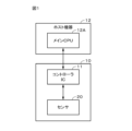
- FIG. 1 is a block diagram showing an example of the configuration of a sensor module according to an embodiment.
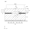
- FIG. 2 is a cross-sectional view showing an example of the configuration of the sensor.
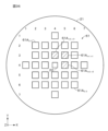
- FIG. 3 is a plan view showing an example of the configuration of the light receiving unit group.
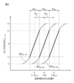
- FIG. 4 is a graph showing an example of the output signal difference SX A1,A4 , the output signal difference SX A2, A4 , and the output signal difference SX A3, A6 .
- FIG. 5 is a graph showing an example of the output signal difference SY B1,B4 , the output signal difference SY B2, B4 , and the output signal difference SY B3, B6 .
- FIG. 1 is a block diagram showing an example of the configuration of a sensor module according to an embodiment.
- FIG. 2 is a cross-sectional view showing an example of the configuration of the sensor.
- FIG. 3 is a plan view showing an example of the configuration of the light receiving unit group.
- FIG. 4 is a graph showing an example
- FIG. 7A is a graph showing an example of the difference between the output signals SX A1 and A4 .
- FIG. 7B is a graph showing an example of the difference between the output signals SX A2 and A5 .
- FIG. 7C is a graph showing an example of the difference between the output signals SX A3 and A6 .
- FIG. 8A is a schematic diagram illustrating an example of a region R A1, A4 in which the output signal difference SX A1, A4 has a small error.
- FIG. 8B is a schematic diagram illustrating an example of a region R A2, A5 in which the output signal difference SX A2, A5 has a small error.
- FIG. 8A is a schematic diagram illustrating an example of a region R A1, A4 in which the output signal difference SX A1, A4 has a small error.
- FIG. 8B is a schematic diagram illustrating an example of a region R A2, A5 in which the output signal difference SX A2, A5 has a small error.
- FIG. 8C is a schematic diagram illustrating an example of a region R A3, A6 in which the output signal difference SX A3, A6 has a small error.
- FIG. 8D is a schematic diagram showing an example of a region R A1, A6 in which the region R A1, A4 , the region R A2, A5 , and the region R A3 , A6 are integrated.
- FIG. 9A is a graph showing an example of the difference between the output signals SY B1 and B4 .
- FIG. 9B is a graph showing an example of the difference between the output signals SY B2 and B5 .
- FIG. 9C is a graph showing an example of the difference between the output signals SY B3 and B6 .
- FIG. 10A is a schematic diagram illustrating an example of regions R A1, A4 in which the output signal differences SY B1, B4 have small errors.
- FIG. 10B is a schematic diagram illustrating an example of a region R A2, A5 in which the output signal difference SY B2, B5 has a small error.
- FIG. 10C is a schematic diagram showing an example of a region R A3, A6 in which the output signal difference SY B3, B6 has a small error.
- FIG. 10D is a schematic diagram showing an example of a region R B1, B6 in which the region R B1, B4 , the region R B2, B5 , and the region R B3 , B6 are integrated.
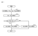
- FIG. 11 is a flowchart for explaining an example of the force FZ detection operation by the sensor module.
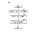
- FIG. 12 is a flowchart for explaining an example of the first detection operation of the forces F X and F Y by the sensor module.
- FIG. 13 is a flowchart for explaining an example of the second detection operation of the forces F X and F Y by the sensor module.
- FIG. 14A is a side view showing a model for optical simulation.
- FIG. 14B is a plan view showing an optical simulation model.
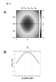
- FIG. 15 is a diagram showing the illuminance distribution determined by optical simulation.
- FIG. 16A is a diagram showing the signal sum SZ obtained by optical simulation.
- FIG. 16B is a graph showing the signal sum SZ at the position of the broken line in FIG. 16A.
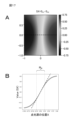
- FIG. 17A is a diagram showing the output signal difference SX determined by optical simulation.
- FIG. 17B is a graph showing the output signal difference SX at the position of the broken line in FIG. 17A.
- FIG. 18 is a diagram showing the output signal difference SY determined by optical simulation.
- FIG. 19A is a perspective view showing an example of the shape of a sensor of Modification 1.
- FIG. 19B is a cross-sectional view taken along line XIXB-XIXB in FIG. 19A.
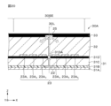
- FIG. 20 is an enlarged cross-sectional view of a portion of FIG. 19B.
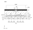
- FIG. 21 is a cross-sectional view showing an example of the configuration of a sensor according to modification 2.
- FIG. 22 is a cross-sectional view showing an example of the configuration of a sensor according to modification 3.
- FIG. 19A is a perspective view showing an example of the shape of a sensor of Modification 1.
- FIG. 19B is a cross-sectional view taken along line XIXB-XIXB in FIG. 19A.
- FIG. 20 is an enlarged cross-
- FIG. 23 is a cross-sectional view showing an example of the configuration of a sensor according to modification 4.
- FIG. 24 is a cross-sectional view showing an example of the configuration of a sensor according to modification 5.
- FIG. 25 is a sectional view showing an example of the configuration of a sensor according to modification 6.
- FIG. 26 is a cross-sectional view showing an example of the configuration of a sensor according to modification 7.
- FIG. 27 is a cross-sectional view showing an example of the configuration of a sensor according to modification 8.
- FIG. 28 is a cross-sectional view showing an example of the configuration of a sensor according to modification 9.
- FIG. 29 is a plan view showing an example of the configuration of the light receiving section.
- FIG. 30 is a sectional view showing an example of the configuration of a sensor according to modification 10.
- FIG. 31 is a cross-sectional view showing an example of the configuration of a sensor according to modification 11.
- FIG. 32 is a plan view showing an example of the configuration of a light receiving unit group according to modification 12.
- FIG. 33 is a plan view showing an example of the configuration of the light receiving section.
- FIG. 34 is a plan view for explaining an example of the detection operation of the forces F X and F Y by the sensor module.
- FIG. 35 is a plan view for explaining an example of the detection operation of the forces F X and F Y by the sensor module.
- FIG. 36 is a plan view for explaining an example of the detection operation of the forces F X and F Y by the sensor module.
- FIG. 37 is a plan view for explaining an example of the detection operation of the forces F X and F Y by the sensor module.
- FIG. 38 is a plan view showing an example of the configuration of a light receiving unit group according to modification 13.
- FIG. 39 is a schematic diagram showing an example of the configuration of the robot hand of Specific Example 1.
- FIG. 40 is a schematic diagram showing an example of the configuration of a robot hand according to specific example 2.
- FIG. 41 is a schematic diagram showing an example of the configuration of a robot hand according to specific example 3.
- FIG. 1 is a block diagram showing an example of the configuration of a sensor module 10 according to an embodiment.
- the sensor module 10 includes a sensor 20 and an IC 11.
- the sensor module 10 may be included in a robot hand, an electronic device, or the like.
- the sensor module 10 is connected to, for example, a main CPU (Central Processing Unit) 12A included in the host device 12.
- a main CPU Central Processing Unit
- FIG. 2 is a cross-sectional view showing an example of the configuration of the sensor 20.
- the sensor 20 is an optical three-axis force sensor.
- the sensor 20 includes a base material 21 , a light source 22 , a light receiving section group 23 , an elastic body 24 , a reflecting section 25 , and a light shielding layer 26 .
- the sensor 20 has a dome shape.
- the dome shape refers to a hemispherical shape or a convex shape similar to the hemispherical shape.
- the convex shape includes shapes such as a substantially parabolic shape, a substantially hemispherical shape, and a substantially semiellipsoidal shape.
- the sensor 20 has a central axis 20L that passes through the top of the dome-shaped curved surface and the center of the circular bottom surface when no force is applied to the dome-shaped curved surface of the sensor 20.
- the base material 21 supports the light source 22, the light receiving unit group 23, the elastic body 24, and the light shielding layer 26.
- the base material 21 has a first surface facing the reflective section 25 and a second surface opposite to the first surface.
- the direction parallel to the central axis 20L that is, the direction perpendicular to the first surface of the base material 21 is referred to as the Z direction (third direction).
- Two directions that are orthogonal to the Z direction and mutually orthogonal, that is, two directions that are orthogonal to each other in a plane parallel to the first surface of the base material 21 are referred to as the X direction (first direction) and the Y direction (second direction).
- the first surface and the second surface have a circular shape in plan view.
- a planar view refers to a planar view when the object is viewed from the +Z direction or the -Z direction.
- the base material 21 may include a light absorption layer on the first surface side.
- the light source 22, the light receiving unit group 23, the elastic body 24, and the light shielding layer 26 are provided on the first surface of the base material 21.
- the light source 22 and/or the light receiving unit group 23 may be directly formed on the first surface of the base material 21, or may be bonded together.
- "and/or” means at least one of them; for example, "X and/or Y” means three types: X only, Y only, and X and Y.
- the center position of the reflective surface of the reflective section 25 in the Z direction with respect to the first surface of the base material 21 is referred to as the height Z of the reflective section 25 or the position Z of the reflective section 25.
- the center position of the reflective surface of the reflective section 25 in the X direction with respect to the central axis 20h of the base material 21 is referred to as the position X of the reflective section 25.
- the center position of the reflective surface of the reflective section 25 in the Y direction with respect to the central axis 20h of the base material 21 is referred to as a position Y of the reflective section 25.
- the reflective surface center position represents the geometric center position of the reflective surface in plan view.
- the base material 21 is, for example, a substrate or a film.
- the substrate may be rigid or flexible.
- the substrate may be made of, for example, a semiconductor in which the light source 22 and/or the light receiving unit group 23, etc. can be easily formed, or may be made of glass or resin that has low moisture and oxygen permeability.
- the substrate may be a semiconductor substrate, a glass substrate, a resin substrate, or the like.
- the semiconductor substrate includes, for example, amorphous silicon, polycrystalline silicon, single crystal silicon, or the like.
- the glass substrate includes, for example, high strain point glass, soda glass, borosilicate glass, forsterite, lead glass, or quartz glass.
- the resin substrate includes, for example, at least one selected from the group consisting of polymethyl methacrylate, polyvinyl alcohol, polyvinylphenol, polyether sulfone, polyimide, polycarbonate, polyethylene terephthalate, polyethylene naphthalate, and the like.
- the base material 21 may include an insulating layer on the first surface side, if necessary.
- the light source 22 can emit light toward the reflecting section 25 .
- the light that the light source 22 can emit is not particularly limited, and may be any of visible light, ultraviolet light, and infrared light, for example.
- the visible light may be white light, red light, green light, blue light, or light of a color other than these.
- the light source 22 is provided at the geometric center of the first surface of the base material 21 .
- the light source 22 is located directly below the reflecting section 25 in a state where no force is acting on the dome-shaped curved surface of the sensor 20.
- the geometric center position of the light emitting surface of the light source 22 (hereinafter simply referred to as "center position of the light source 22") is located on the central axis 20L when no force is acting on the dome-shaped curved surface of the sensor 20.
- the light source 22 includes, for example, a light emitting element such as an LED (Light Emitting Diode) element, an LD (Laser Diode) element, an SLD (Super Luminescent Diode) element, or an OLED (Organic Light Emitting Diode) element.
- the light source 22 may be an SMD (Surface Mount Device) in which a light emitting element is packaged, or may be a light emitting element wired on the base material 21 by wire bonding or the like.
- FIG. 3 is a plan view showing an example of the configuration of the light receiving unit group 23.
- the light receiving section group 23 includes first light receiving sections 23A 1 to 23A 6 and second light receiving sections 23B 1 to 23B 6 .
- the first light receiving sections 23A 1 to 23A 6 may be collectively referred to as the first light receiving section 23A.
- the second light receiving sections 23B 1 to 23B 6 may be collectively referred to as the second light receiving section 23B.
- the sensor 20 includes six first light receiving sections 23A 1 to 23A 6 and six second light receiving sections 23B 1 to 23B 6 .
- the number of second light receiving sections 23B is not limited to this.
- the number of first light receiving sections 23A and second light receiving sections 23B may be four, five, or seven or more. It is preferable that the number of first light receiving sections 23A and second light receiving sections 23B is an even number.
- the first light receiving sections 23A 1 , 23A 6 and the second light receiving sections 23B 1 , 23B 6 may be used when the height Z of the reflecting section 25 is high, for example, when the height Z is in the range h 1 ⁇ Z. good.
- the first light receiving sections 23A 3 , 23A 4 and the second light receiving sections 23B 3 , 23B 4 are used when the height Z of the reflecting section 25 is low, for example, when the height Z of the reflecting section 25 is in the range of Z ⁇ h 2 . May be used for.
- the first light receiving sections 23A 2 , 23A 5 and the second light receiving sections 23B 2 , 23B 5 may be used, for example, when Z is in the range h 2 ⁇ Z ⁇ h 1 .
- all of the first light receiving sections 23A 1 to 23A 6 may be used regardless of the height Z of the reflecting section 25.
- the second light receiving sections 23B 1 to 23B 6 are switched and used as a pair, all of the second light receiving sections 23B 1 to 23B 6 may be used regardless of the height Z of the reflecting section 25.
- the first light receiving sections 23A 1 to 23A 6 and the second light receiving sections 23B 1 to 23B 6 can receive the light reflected by the reflecting section 25.
- the first light receiving sections 23A 1 to 23A 6 and the second light receiving sections 23B 1 to 23B 6 can convert the received light into electrical signals and supply them to the IC 11.
- the first light receiving sections 23A 1 to 23A 6 are arranged in the X direction and form a column.
- the first light receiving sections 23A 1 to 23A 6 forming the row are arranged symmetrically with respect to the center of the light receiving section group 23, that is, with respect to the geometric center of the light source 22.
- the second light receiving sections 23B 1 to 23B 6 are arranged in the Y direction and form a column.
- the second light receiving sections 23B 1 to 23B 6 forming the row are arranged symmetrically with respect to the center of the light receiving section group 23, that is, with respect to the geometric center of the light source 22.
- Each of the first light receiving sections 23A 1 to 23A 6 and the second light receiving sections 23B 1 to 23B 6 includes one or more light receiving elements.
- the light receiving element is, for example, a photodiode, an avalanche photodiode, or a phototransistor.
- the first light receiving sections 23A 1 to 23A 6 and the second light receiving sections 23B 1 to 23B 6 may each be an SMD (Surface Mount Device) in which one or more light receiving elements are packaged, or may be formed by wire bonding or the like. It may be one or more light receiving elements wired on the base material 21.
- SMD Surface Mount Device
- the first light receiving sections 23A 1 to 23A 6 and the second light receiving sections 23B 1 to 23B 6 may be mounted on the base material 21 via connecting members such as bumps, or may be mounted on the base material 21 by patterning, for example, amorphous silicon or the like. Accordingly, it may be formed directly on the base material 21.
- h is the height of the reflective surface of the reflective section 25 with respect to the first surface of the base material 21.
- D is the distance from the center position of the light source 22 (that is, the intersection position of the central axis 20L and the first surface of the base material 21) to the center position of the first light receiving part 23A 2 or the center position of the second light receiving part 23B 2 . be.
- the center position of the first light receiving part 23A 2 and the second light receiving part 23B 2 represents the geometric center position of the first light receiving part 23A 2 and the second light receiving part 23B 2 in plan view.
- the center position of the light source 22 represents the geometric center position of the light output surface of the light source 22 in plan view.
- the arrangement of the first light receiving sections 23A 1 to 23A 6 and the second light receiving sections 23B 1 to 23B 6 is preferably adjusted based on a state in which the distance between the reflecting section 25 and the base material 21 is close.
- the first light receiving sections 23A 1 to 23A 6 and the second light receiving sections 23B 1 to 23B 6 have a light distribution distribution of reflected light by the reflecting section 25 (see FIG. ) is preferably provided within a linear region that changes approximately linearly.
- the light distribution of the light reflected by the reflecting section 25 described above is the light distribution of the light reflected by the reflecting section 25 in a state where no forces are acting on the sensor 20 in the ⁇ X direction, ⁇ Y direction, and -Z direction.
- the light distribution may be as follows.
- the elastic body 24 can be elastically deformed in the ⁇ X direction, ⁇ Y direction, and ⁇ Z direction.
- the elastic body 24 is transparent to the light emitted from the light source 22.
- the light source 22 is configured to emit visible light such as white light, red light, green light, or blue light
- the elastic body 24 is transparent to visible light. It's okay.
- the elastic body 24 may be colored.
- the elastic body 24 has a dome shape.
- the elastic body 24 supports the reflective section 25 at its dome-shaped top.
- the elastic body 24 is provided between the reflecting section 25 and the light receiving section group 23.
- the elastic body 24 is arranged on the first surface of the base material 21 such that the bottom surface of the elastic body 24 is on the first surface side of the base material 21.
- the elastic body 24 includes, for example, at least one of an elastomer and a gel.
- the elastomer includes, for example, at least one selected from the group consisting of silicone elastomer, acrylic elastomer, urethane elastomer, styrene elastomer, and the like.
- the gel includes, for example, at least one polymer gel selected from the group consisting of silicone gel, urethane gel, acrylic gel, and styrene gel.
- materials having various hardnesses can be selected. By selecting the material hardness of the elastic body 24, it is possible to adjust the sensitivity range of the sensor 20.
- the reflecting section 25 can reflect the light emitted from the light source 22 toward the first surface of the base material 21 . That is, the reflecting section 25 can reflect the light emitted from the light source 22 toward the first surface of the light receiving section group 23 .
- the reflection by the reflection section 25 is, for example, specular reflection or diffuse reflection.
- the reflecting portion 25 has, for example, a reflecting surface that reflects the light emitted from the light source 22 and a back surface opposite to the reflecting surface.
- the reflective surface is, for example, a mirror surface or a diffusive surface.
- the reflecting section 25 is provided above the light receiving section group 23.
- the reflector 25 is located directly above the light source 22 when no force is applied to the dome-shaped curved surface of the sensor 20 .
- the geometric center position of the reflective surface of the reflective section 25 (hereinafter simply referred to as "center position of the reflective section 25") is aligned with the central axis 20L. located above.
- the reflective surface of the reflective section 25 is held parallel to the first surface of the base material 21.
- the reflective section 25 is held on the top of the elastic body 24.
- the center position (position in the X direction, Y direction, and Z direction) of the reflecting part 25 changes as the elastic body 24 deforms. Due to this positional change, the orientation distribution of reflected light by the reflecting section 25 is changed.
- the reflecting portion 25 has, for example, a circular shape or a regular polygonal shape (for example, a square shape) in plan view.
- the reflective section 25 is a reflective layer capable of specular reflection or a diffuse reflective layer capable of diffuse reflection (scattering).
- the reflective layer is, for example, a metal layer.
- the metal layer include chromium (Cr), gold (Au), platinum (Pt), nickel (Ni), copper (Cu), molybdenum (Mo), titanium (Ti), tantalum (Ta), and aluminum (Al). , magnesium (Mg), iron (Fe), tungsten (W), and silver (Ag).
- the diffuse reflection layer contains particles as light scatterers, for example. More specifically, the diffuse reflection layer is a white layer containing white silicone or the like, a white film (eg, white PET film), or the like.
- the light shielding layer 26 can absorb incident light.
- the incident light is, for example, external light, light emitted from the light source 22, or the like.
- the light shielding layer 26 can be deformed together with the elastic body 24.
- the light shielding layer 26 is provided on the dome-shaped curved surface of the elastic body 24 and covers the dome-shaped curved surface of the elastic body 24 and the back surface (the surface opposite to the reflective surface) of the reflective section 25.
- the light-shielding layer 26 includes, for example, a light-absorbing material and a binder.
- the light absorbing material includes, for example, a black pigment.
- the black pigment includes, for example, at least one selected from the group consisting of carbon black, titanium black, and the like. Titanium black is black particles containing titanium atoms, and preferably contains at least one of lower titanium oxide and titanium oxynitride. The black pigment may be surface-modified as necessary for the purpose of improving dispersibility and suppressing agglomeration.
- the light shielding layer 26 may contain, for example, black silicone.
- the binder has elasticity.
- the binder includes, for example, at least one selected from the group consisting of silicone resins, acrylic resins, urethane resins, and the like.
- the IC 11 drives the light source 22 and causes the light source 22 to emit light toward the reflecting section 25 .
- the IC 11 scans the first light receiving portions 23A 1 to 23A 6 and the second light receiving portions 23B 1 to 23B 6 , obtains output signals S A1 to S A6 from the first light receiving portions 23A 1 to 23A 6 , and scans the second light receiving portions 23A 1 to 23A 6 .
- Output signals S B1 to S B6 are obtained from 23B 1 to 23B 6 .
- the order in which the IC 11 scans the first light receiving sections 23A 1 to 23A 6 and the second light receiving sections 23B 1 to 23B 6 is not particularly limited.
- the distance between the center position of the reflection part 25 and the base material 21 becomes shorter (that is, as the center position of the reflection part 25 in the Z direction becomes lower), the light distribution of the light reflected by the reflection part 25 is reduced. Therefore, as the distance between the center position of the reflecting section 25 and the base material 21 becomes shorter, the area where the detection error of the sum SZ of the output signals is small with respect to a change in the position of the reflecting section 25 in the X and Y directions becomes narrower.
- the region in which the detection error of the sum SZ of the output signals is small represents a region in which the sum SZ of the output signals remains approximately constant with respect to changes in the position of the reflecting section 25 in the X and Y directions.
- the sum SZ of the output signals corresponds to the force (pressing force) FZ acting in the Z direction.
- the sum SZ of the output signals changes approximately linearly with respect to changes in the distance between the center position of the reflecting section 25 and the base material 21.
- the IC 11 operates as follows depending on the distance between the reflection section 25 and the base material 21.
- the IC 11 calculates the force FZ acting in the Z direction based on the sum SZ1 of the output signals, and outputs it to the main CPU 12A. do.
- the IC 11 calculates the force FZ acting in the Z direction based on the sum SZ2 of the output signals, and sends the calculated force FZ to the main CPU 12A. Output.
- the dynamic range of the sensor module 10 can be expanded by the IC 11 performing position detection processing according to the distance between the center position of the reflecting section 25 and the base material 21 as described above.
- the IC 11 determines whether the distance between the center position of the reflecting section 25 and the base material 21 has become closer than a specified value based on whether the sum of the output signals SZ 1 is greater than the specified value SZ 0 . That is, when the sum SZ 1 of the output signals is larger than the specified value SZ 0 , the IC 11 determines that the distance between the center position of the reflecting section 25 and the base material 21 is farther than the specified value. On the other hand, when the sum SZ 1 of the output signals is less than or equal to the specified value SZ 0 , the IC 11 determines that the distance between the center position of the reflecting section 25 and the base material 21 is closer than the specified value.
- the IC 11 operates as follows when the distance between the center position of the reflection section 25 and the base material 21 is longer than a specified value.
- the IC 11 calculates the force F X acting in the X direction based on the calculated difference SX A1 and A6 of the output signals, and outputs it to the main CPU 12A.
- the IC 11 calculates the force FY acting in the Y direction based on the calculated difference between the output signals SYB1 and B6 , and outputs it to the main CPU 12A.
- the region where the detection error of the output signal differences SX and SY is small is, as described above, a linear region where the output signal differences SX and SY change approximately linearly with respect to changes in the position of the reflecting section 25 in the X and Y directions. (first and second linear regions).
- the output signal difference SX corresponds to the force F X acting in the X direction
- the output signal difference SY corresponds to the force F Y acting in the Y direction.
- the IC 11 operates as follows when the distance between the center position of the reflection section 25 and the base material 21 is closer than a specified value.
- the IC 11 calculates the force F X acting in the X direction using the pair of output signals SA m and SA n that can minimize the detection error of the force F X among the pair of output signals SA m and SA n . calculate. Further, the IC 11 uses the pair of output signals SB m and SB n that can minimize the detection error of the force F Y among the pair of output signals SB m and SB n to detect the force F acting in the Y direction. Calculate Y.
- the pair of output signals SA m , SA n used for calculating the above - mentioned force F , 23A n pair of output signals output from the pair SA m , SA n .
- 23A 6 is a pair of output signals SA 3 , SA 6 .
- the pair of output signals SB m and SB n used for calculating the above-mentioned force F Y is, for example, straddled over the center of the light receiving section group 23, that is, across the light source 22, and sent to the second light receiving section 23B m separated by a specified distance.
- 23B n pairs of output signals SB m and SB n .
- the pair of output signals SB 1 and SB 4 of the second light receiving sections 23B 1 and 23B 4 , the pair of output signals SB 2 and SB 5 of the second light receiving sections 23B 2 and 23B 5 , and the second light receiving section This is a pair of output signals SB 3 and SB 6 of 23B 3 and 23B 6 .
- the IC 11 operates as follows.
- the IC 11 calculates the center positions X A1,A4 , X A2,A5 , and X A3,A6 of the reflecting section 25 as follows.
- the output signal difference SX A1, A4 is a value corresponding to the amount of displacement of the center position of the reflecting section 25 in the X direction with the center axis 20L as a reference.
- the IC 11 calculates the center positions X A1, A4 of the reflecting section 25 based on the calculated difference SX A1 , A4 between the output signals.
- the center positions It is determined by the following equation (1-1) using the output signals S A1 , S A4 ) obtained from the four pairs of light receiving sections 23A 1 and 23A.
- X A1, A4 -D 11 + (d 11 /L) x SX A1, A4 ... (1-1)
- D 11 is the position of the midpoint between the four pairs of first light receiving sections 23A 1 and 23A
- d 11 is (the width of the linear region of SX A1, A4 in the X direction)/2.
- linear region refers to a linear region (first and second linear regions) in which the output signal differences SX Am,An and SY Bm,Bn change approximately linearly with respect to changes in the position of the reflecting section 25 in the X and Y directions. ) represents.
- the output signal difference SX A2, A5 is a value corresponding to the amount of displacement of the center position of the reflecting section 25 in the X direction with the center axis 20L as a reference.
- the IC 11 calculates the center position X A2, A5 of the reflecting section 25 based on the calculated difference SX A2 , A5 between the output signals.
- the output signal difference SX A3, A6 is a value corresponding to the amount of displacement of the center position of the reflecting section 25 in the X direction with the center axis 20L as a reference.
- the IC 11 calculates the center positions X A3, A6 of the reflecting section 25 based on the calculated difference SX A3 , A6 between the output signals.
- the center positions It is determined by the following equation (1-3) using the output signals S A3 , S A6 ) obtained from the six pairs of light receiving sections 23A 3 and 23A.
- X A3, A6 D 12 + (d 13 /L) x SX A3, A6 ... (1-3)
- D 12 is the position of the midpoint between the six pairs of first light receiving sections 23A 3 and 23A
- d 13 is (the width of the linear region of SX A3 and A6 in the X direction)/2.
- the IC 11 selects X Am, An included in the linear region from among X A1, A4 , X A2, A5 , and X A3, A6 .
- X Am an included in the linear region
- the IC 11 selects the X Am, An as the X Am, An with the least error.
- IC11 selects the X that is closest to the center position of the linear region among the two or more X Am, An. Let Am, An be X Am, An with the least error.
- the IC 11 calculates the force F X acting in the X direction using X Am and An with the least error. More specifically, for example, the IC 11 calculates the difference in output signals (difference in sensor output values) SX Am, An from X Am , An with the smallest error. Alternatively, the IC 11 calculates the output signal difference SX Am, An corresponding to the smallest error among the output signal differences SX A1,A4 , SX A2,A5 , and SX A3, A6 calculated in advance. Select.
- the IC 11 calculates the force F X acting in the X direction based on the calculated or selected output signal difference SX Am, An , and outputs it to the main CPU 12A.
- the IC 11 calculates the center positions Y B1,B4 , Y B2,B5 , and Y B3,B6 of the reflecting section 25 as follows.
- the difference between the output signals SY B1 and B4 is a value corresponding to the amount of displacement of the center position of the reflecting section 25 in the Y direction with respect to the central axis 20L.
- the IC 11 calculates the center positions Y B1 and B4 of the reflecting section 25 based on the calculated difference SY A1 and A4 between the output signals.
- the center positions YB1,B4 of the reflecting section 25 are determined by the difference between the output signals SYB1,B4 (that is, the It is determined by the following equation (2-1) using the output signals S B1 , S B4 ) obtained from the four pairs of two light receiving sections 23B 1 and 23B.
- Y B1, B4 -D 21 + (d 21 /L) x SY B1, B4 ... (2-1)
- D 21 is the position of the midpoint between the four pairs of second light receiving sections 23B 1 and 23B
- d 21 is (width of the linear region of SY B1, B4 in the Y direction)/2.
- the difference between the output signals SY B2 and B5 is a value corresponding to the amount of displacement of the center position of the reflecting section 25 in the Y direction with respect to the central axis 20L.
- the IC 11 calculates the center position Y B2, B5 of the reflecting section 25 based on the calculated difference SY B2 , B5 between the output signals.
- the center positions Y B2, B5 of the reflecting section 25 are determined by the difference SY B2, B5 (i.e., the difference between the output signals SY B2, B5 ). It is determined by the following equation (2-2) using the output signals S B2, S B5 ) obtained from the five pairs of two light receiving sections 23B 2 and 23B.
- Y B2, B5 (d 22 /L) x SY B2, B5 ... (2-2)
- d22 is (the width of the linear region of SY B2 and B5 in the Y direction)/2.
- the difference between the output signals SY B3 and B6 is a value corresponding to the amount of displacement of the center position of the reflecting section 25 in the Y direction with respect to the central axis 20L.
- the IC 11 calculates the center positions Y B3, B6 of the reflecting section 25 based on the calculated difference SY B3 , B6 between the output signals.
- the center positions YB3,B6 of the reflecting section 25 are determined by the difference SYB3,B6 (i.e., the difference SYB3,B6) between the output signals. It is determined by the following equation (2-3) using the output signals S B3 , S B6 ) obtained from the six pairs of two light receiving sections 23B 3 and 23B.
- Y B3, B6 D 22 + (d 23 /L) x SY B3, B6 ... (2-3)
- D 22 is the position of the midpoint between the six pairs of second light receiving sections 23B 3 and 23B
- d 23 is (the width of the linear region of SY B2 and B5 in the Y direction)/2.
- the IC 11 selects Y Bm, Bn included in the linear region from Y B1, B4 , Y B2, B5 , and Y B3, B6 .
- the IC 11 selects the Y Bm, Bn as the Y Bm, Bn with the smallest error.
- IC11 selects the Y Bm , Bn that is closest to the center position of the linear region among the two or more Y Bm, Bn. Let Bm, Bn be Y Bm, Bn with the least error.
- the IC 11 calculates the force F Y acting in the Y direction using Y Bm and Bn with the least error. More specifically, for example, the IC 11 calculates the difference in output signals (difference in sensor output values) SY Bm, Bn from Y Bm, Bn with the smallest error. Alternatively, the IC 11 selects the output signal difference SY Bm, Bn corresponding to the least error Y Bm, Bn from among the output signal differences SY B1, B4 , SY B2, B5 , and SY B3, B6 calculated in advance. Select.
- the IC 11 calculates a force F Y acting in the Y direction based on the calculated or selected difference between the output signals SY Bm, Bn , and outputs it to the main CPU 12A.
- the first light receiving section 23A 2 When the light with the light amount Q A2 is received by the first light receiving section 23A 2 , the first light receiving section 23A 2 outputs an output signal S A2 corresponding to the light amount Q A2 .
- the first light receiving section 23A5 receives the light having the light amount Q A5 , the first light receiving section 23A5 outputs an output signal S A2 corresponding to the light amount Q A5 .
- the sum of the light amounts QZ A2, A5 corresponds to the amount of displacement of the center position of the reflecting section 25 in the Z direction.
- the force FZ acting in the Z direction can be calculated.
- the light amount difference QX A2, A5 corresponds to the amount of displacement of the center position of the reflecting section 25 in the ⁇ X direction.
- the force F X acting in the ⁇ X direction can be calculated.
- the light distribution 20I has a conical shape and the slope of the light distribution 20I changes linearly.
- the IC 11 determines the center position As shown in FIGS. 7A and 8A , the area where the detection error of the position Only.
- the IC 11 determines the center position As shown in FIGS . 7B and 8B, the area where the detection error of the position Only.
- the IC 11 determines the center position As shown in FIGS . 7C and 8B, the area where the detection error of the position Only.
- the IC 11 detects the difference SX A1,A4 between the output signals obtained by the four pairs of first light receiving sections 23A 1 and 23A, the difference SX A2,A5 between the output signals obtained from the five pairs of first light receiving sections 23A 2 and 23A, and the first
- the detection error of the position X is as shown in FIG. 8D.
- the areas with a small number of areas are areas R A1 and A6 .
- the area R A1, A6 corresponds to an area where the area R A1, A4 , the area R A2, A5 , and the area R A3, A6 are integrated.
- the IC 11 detects the center position X of the reflecting section 25 using the output signal difference SX A1, A4 , the output signal difference SX A2, A5 , and the output signal difference SX A3, A6 .
- the dynamic lens in the ⁇ X direction can be magnified.
- widths (widths in the X-axis direction) of the regions R A1, A4 , R A2, A5 , R A3, A6, and R A1, A6 are shown below.
- the widths (widths in the X-axis direction) of the regions R A1, A4 , R A2, A5 , and R A3, A6 are each 0.2 mm, for example.
- the four pairs of first light receiving sections 23A 1 and 23A are arranged with a deviation of, for example, 0.1 mm in the -X direction from the five pairs of first light receiving sections 23A 2 and 23A.
- the six pairs of first light receiving sections 23A 3 and 23A are arranged with a deviation of, for example, 0.1 mm from the five pairs of first light receiving sections 23A 2 and 23A in the +X direction.
- the width (width in the X-axis direction) of the region R A1, A6 in which the regions R A1, A4, the region R A2, A5 , and the region R A3, A6 are integrated is, for example, 0.4 mm.
- SY B1 , B4 the region where the detection error of the position Y is small (that is, the linear region where the values of SY B1 and B4 change approximately linearly) is the region R B1, B4 Only.
- SY B2 , B5 the region where the detection error of the position Y is small (that is, the linear region where the values of SY B2 and B5 change approximately linearly) is the region R B2, B5. Only.
- SY B3 , B6 the region where the detection error of the position Y is small (that is, the linear region where the values of SY B3 and B6 change approximately linearly) is the region R B3, B6. Only.
- the IC 11 detects the difference SY A1,A4 between the output signals obtained by the four pairs of second light receiving sections 23B 1 and 23B, the difference SY B2,B5 between the output signals obtained from the five pairs of second light receiving sections 23B 2 and 23B, and the second When the center position Y of the reflecting section 25 is detected using the difference SY B3, B6 between the output signals obtained by the six pairs of light receiving sections 23B 3 and 23B, the detection error of the position Y is as shown in FIG. 10D.
- the regions with a small amount of data are regions R B1 and B6 .
- the area R B1, B6 corresponds to an area where the area R B1, B4 , the area R B2, B5 , and the area R B3, B6 are integrated.
- the IC 11 detects the center position Y of the reflecting section 25 using the output signal difference SY B1, B4 , the output signal difference SY B2, B5 , and the output signal difference SY B3, B6 .
- the dynamic lens in the ⁇ Y direction can be magnified.
- widths (widths in the Y-axis direction) of the regions R B1, B4 , R B2, B5 , R B3, B6, and R B1, B6 are shown below.
- the widths (width in the Y-axis direction) of the regions R B1, B4 , R B2, B5 , and R B3, B6 are each 0.2 mm, for example.
- the four pairs of second light receiving sections 23B 1 and 23B are arranged with a deviation of, for example, 0.1 mm from the five pairs of second light receiving sections 23B 2 and 23B in the +Y direction.
- the six pairs of second light receiving sections 23B 3 and 23B are arranged with a deviation of, for example, 0.1 mm from the five pairs of second light receiving sections 23B 2 and 23B in the -Y direction.
- the width (width in the Y-axis direction) of the region R B1, B6 in which the region R B1, B4, the region R B2, B5 , and the region R B3, B6 are integrated is, for example, 0.6 mm.
- step S11 the IC 11 scans the first light receiving sections 23A 1 to 23A 6 and the second light receiving sections 23B 1 to 23B 6 , and outputs signals S A1 to S A6 from the first light receiving sections 23A 1 to 23A 6 .
- Output signals S B1 to S B6 are obtained from the second light receiving sections 23B 1 to 23B 6 .
- step S12 the IC 11 receives the output signals S A1 , S A6 of the six pairs of first light receiving sections 23A 1 , 23A and the output signals S B1 , S B6 of the six pairs of second light receiving sections 23B 1 , 23B.
- step S13 the IC 11 determines whether the calculated sum SZ1 of the output signals is greater than or equal to a specified value. If it is determined in step S13 that the sum SZ1 of the output signals is equal to or greater than the specified value, the IC 11 calculates the force FZ based on the sum SZ1 of the output signals in step S14. If it is determined in step S13 that the sum SZ1 of the output signals is not equal to or greater than the specified value, the IC 11 calculates the force FZ based on the sum SZ2 of the output signals in step S15, and outputs it to the main CPU 12A.
- the first detection operation is performed, for example, when it is determined in step S13 of FIG. 11 that the sum SZ1 of the output signals is equal to or greater than a specified value.
- step S21 the IC 11 scans the first light receiving sections 23A 1 , 23A 6 and the second light receiving sections 23B 1 , 23B 6 , and outputs signals S A1 , S A6 , from the first light receiving sections 23A 1 , 23A 6 .
- Output signals S B1 and S B6 are obtained from the second light receiving sections 23B 1 and 23B 6 .
- the IC 11 uses the output signals S A1 and S A6 and the output signals S B1 and S B6 obtained in step S11 in FIG . It may be calculated. In this case, the process of step S21 may be omitted.
- step S23 the IC 11 calculates the force F X based on the difference between the output signals SX A1 and A6 , and calculates the force F Y based on the difference between the output signals SY B1 and B6 .
- the IC 11 outputs the calculated force F X and force F Y to the main CPU 12A.
- the second detection operation is performed, for example, when it is determined in step S13 of FIG. 11 that the sum SZ1 of the output signals is not equal to or greater than the specified value.
- step S31 the IC 11 scans the first light receiving sections 23A 1 to 23A 6 and the second light receiving sections 23B 1 to 23B 6 , and outputs signals S A1 to S A6 from the first light receiving sections 23A 1 to 23A 6 .
- Output signals S B1 to S B6 are obtained from the second light receiving sections 23B 1 to 23B 6 .
- step S32 the IC 11 determines the center position X A1 , A4 , X A2 , A5 , X A3, A6 , Y B1, B4 , Y B2, B5 , Y B3, B6 are calculated.
- the IC 11 uses the output signals S A1 to S A6 and the output signals S B1 to S B6 obtained in step S11 in FIG . , A6 , Y B1,B4 , Y B2,B5 , Y B3, B6 may be calculated. In this case, the process of step S31 may be omitted.
- step S33 the IC 11 determines whether the calculated center positions X A1, A4 , X A2, A5 , X A3, A6 of the reflecting portion 25 are linear regions R A1, A4 , R A2, A5 , R A3, A6 (see FIGS. 7A, 7B, and 7C) is determined, and X Am , An included in the linear region R Am, An is selected.
- IC11 is such that Y B1, B4 , Y B2, B5 , Y B3, B6 are included in the linear regions R B1, B4 , R B2, B5 , R B3, B6 (see FIGS. 9A, 9B, and 9C), respectively.
- X Bm, Bn included in the linear region R Bm, Bn are selected.
- step S34 the IC 11 selects the X Am, An closest to the center position of the linear region R Am, An from among the X Am, An selected in step S33 (FIG. 7A, FIG. 7B, 7C, FIG. 8A, FIG. 8B, FIG. 8C, and FIG. 8D). 7A, FIG. 7B, FIG. 7C, FIG. 8A, FIG. 8B, FIG. 8C, and FIG. 8D, X 1 , X 2 , and Represents the center position. If the number of X Am, An selected in step S33 is one, the IC 11 does not need to perform this process.
- step S34 the IC 11 selects Y Bm, Bn closest to the center position of the linear region R Bm, Bn from among the Y Bm, Bn selected in step S33 (FIGS. 9A, 9B, 9C , FIG. 10A, FIG. 10B, FIG. 10C, and FIG. 10D).
- 9A, FIG. 9B, FIG. 9C, FIG. 10A, FIG . 10B , FIG . 10C , and FIG. Represents the center position. If the number of Y Bm and Bn selected in step S33 is one, the IC 11 does not need to perform this process.
- step S35 the IC 11 calculates the difference in output signals (difference in sensor output values) SX Am,An , SY Am,An from X Am,An , YBm , Bn selected in step S34. calculate.
- the IC 11 calculates the forces F X and F Y acting in the X and Y directions based on the calculated output signal differences SX Am,An and SY Am,An , and outputs them to the main CPU 12A.
- Point light source 72 corresponds to reflective portion 25 of sensor 20 in one embodiment.
- the irradiation surface 70S corresponds to the first surface of the base material 21 (the surface on which the light receiving unit group 23 is arranged) in one embodiment.
- the first light receiving sections 71A 1 and 71A 2 correspond to the first light receiving sections 23A 2 and 23A 5 in one embodiment.
- the second light receiving sections 71B 1 and 71B 2 correspond to the second light receiving sections 23B 2 and 23B 5 in one embodiment.
- the distance D Y between the center position 70P of 70S and the center positions of the second light receiving sections 71B 1 and 71B 2 is as follows. However, the center position 70P is set directly below the point light source 72. Height h: 1.0 Distance DX : 0.5 Distance DY : 0.5
- the sum SZ of the output signals is the sum of the output signals S A1 , S A2 of the first light receiving sections 71A 1 , 71A 2 and the output signals S B1 , S B2 of the second light receiving sections 71B 1 , 71B 2 (S A1 +S A2 +S B1 +S B2 ).
- the difference between the output signals SX A1 and A2 is the difference (S A1 - S A2 ) between the output signals S A1 and S A2 of the first light receiving sections 71A 1 and 71A 2 .
- the difference between the output signals SY B1 and B2 is the difference (S B1 - S B2 ) between the output signals S B1 and S B2 of the second light receiving sections 71B 1 and 71B 2 .
- FIGS. 16A, 16B, 17A, 17B, and 18 The results of the above optical simulation are shown in FIGS. 16A, 16B, 17A, 17B, and 18.
- a prescribed region RB in which the detection error of the force (shear force) FX is small is shown in FIG. 14A.
- the sum SZ of the output signals is a substantially constant value in the specified area RA , but changes outside the specified area RA . Therefore, while the detection error of the force (pressing force) FZ corresponding to the sum SZ of the output signals is small in the specified area RA , the error is large outside the specified area RA .
- the difference between the output signals SX A1 and A2 changes substantially linearly in the specified region RB , but does not change substantially linearly outside the specified region RB . Therefore, the detection error of the force ( shearing force) F It is large outside the region RA (that is, when the deformation of the sensor in the X direction is large). Therefore, the dynamic range of the force (shear force) FX acting in the X direction is limited. Further, the amount of change in the output signal difference SX A1, A2 outside the specified area RA is smaller than the amount of change in the output signal difference SX A1, A2 in the specified area RA . Therefore, the sensitivity of force ( shear force) F ) force (shear force) F is lower than the sensitivity of X.
- the output signal difference SY B1, B2 has the same tendency as the output signal difference SX A1, A2 described above.
- the light emitted upward from the light source 22 is reflected by the reflecting section 25 and then transmitted to the first light receiving sections 23A 1 to 23A 6 and the second light receiving sections 23B 1 to 23B 6 . incident.
- the elastic body 24 is deformed, and the center position of the reflecting portion 25 is displaced in at least one of the ⁇ X direction, ⁇ Y direction, and ⁇ Z direction.
- the orientation distribution of the reflected light from the reflecting section 25 changes with the displacement of the center position of the reflecting section 25 described above.
- the amount of light received by each of the first light receiving sections 23A 1 to 23A 6 and the second light receiving sections 23B 1 to 23B 6 changes in accordance with the change in the orientation distribution, and
- the output signals SA 1 to SA 6 and SB 1 to SB 6 from the two light receiving sections 23B 1 to 23B 6 change .
- the IC can detect the forces F X , F Y , and F Z acting on the sensor 20 based on the output signals SA 1 to SA 6 and SB 1 to SB 6 .
- the sensor 20 has the first light receiving sections 23A 1 to 23A 6 arranged in the X direction (first direction) and the first light receiving parts 23A 1 to 23A 6 arranged in the Y direction (second direction) orthogonal to the X direction. 23B 1 to 23B 6 .
- the area (linear area) where the detection error of position and Y position can be reduced can be expanded (area R A2, A5 in FIG. 8B, area R A1, A6 in FIG. 8D, area R B2, B5 in FIG. 10B, area R B2, B5 in FIG. 10D). (Refer to areas R B1 and B6 ).
- the Z position Compared to a sensor including a pair of first light receiving sections 23A 2 and 23A 5 arranged in the X direction and a pair of second light receiving sections 23B 2 and 23B 5 arranged in the Y direction, the Z position The area (linear area) in which the detection error of can be reduced can be expanded. Therefore, a wide dynamic range and high sensitivity can be obtained with respect to the force F Z acting in the -Z direction (that is, the displacement of the reflecting section 25 in the -Z direction).
- FIG. 19A is a plan view showing an example of the appearance of a sensor 30A of Modification 1.
- FIG. 19B is a cross-sectional view taken along line XIXB-XIXB in FIG. 19A.
- FIG. 20 is an enlarged cross-sectional view of a portion of FIG. 19B.
- the sensor 30A is an optical three-axis force sensor.
- the sensor 30A has a planar structure.
- the sensor 30A may have rigidity or flexibility.
- the sensor 30A has, for example, a plate shape or a film shape.
- the sensor 30A has a first surface and a second surface opposite to the first surface.
- the shape of the sensor 30A in a plan view that is, the shapes of the first surface and the second surface in a plan view may be a rectangular shape such as a square shape.
- the shape of the sensor 30A in plan view is not limited to a rectangular shape, but may be a circular shape, an elliptical shape, or the like.
- the sensor 30A has a plurality of sensor sections 30SE.
- the plurality of sensor sections 30SE are two-dimensionally arranged in the in-plane direction (X, Y direction) of the first surface or the second surface of the sensor 30A.
- Each sensor section 30SE has a central axis 30L parallel to the thickness direction of the sensor 30A.
- the central axis 30L passes through the center position of the reflecting section 25 and the center of the light receiving section group 23 in a state where no force is acting on the first surface or the second surface of the sensor 30.
- the direction parallel to the central axis 30L that is, the direction perpendicular to the first surface of the sensor 30A is referred to as the Z direction (third direction).
- Two directions that are orthogonal to the Z direction and mutually orthogonal, that is, two directions that are orthogonal to each other in a plane parallel to the first surface of the sensor 30A are referred to as the X direction (first direction) and the Y direction (second direction).
- the sensor 30A includes a base material layer 31, a plurality of light receiving section groups 23, an elastic layer 32, a plurality of reflection sections 25, and a light shielding layer 33.
- the base material layer 31, the elastic layer 32, and the light-shielding layer 33 are laminated in this order, with the light-shielding layer 33 on the first surface side of the sensor 30A, and the base material layer 31 on the second surface side of the sensor 30A.
- the base material layer 31 includes a base material 31A, a plurality of light sources 22, a bonding layer 31B, a light transmitting layer 31C, and a light blocking layer 31D.
- the base layer 31 may include a reflective layer instead of the light shielding layer 31D.
- the base material 31A can support a plurality of light sources 22 and a light transmitting layer 31C.
- the base material 31A may be the same as the base material 21 in one embodiment in points other than the above.
- the base material 31A may be composed of a reflective layer, or may be composed of a laminate of a substrate or a film and a reflective layer.
- the plurality of light sources 22 are two-dimensionally arranged on the base material 31A in a prescribed arrangement pattern such as a matrix.
- the light source 22 is provided for each sensor section 30SE.
- Each light source 22 is located directly below the pinhole 31DA.
- the bonding layer 31B bonds the base material 31A and the light transmitting layer 31C.
- the bonding layer 31B may cover the light source 22 or may have a hole in the light source 22 portion.
- FIG. 20 shows an example in which the bonding layer 31B has a hole in the light source 22 portion.
- the bonding layer 31B covers the light source 22, it is preferable that the bonding layer 31B has translucency to the light emitted from the light source 22.
- the bonding layer 31B may be translucent to the light emitted from the light source 22, or may be transparent to the light emitted from the light source 22. It may be opaque to the light emitted from 22.
- the bonding layer 31B is provided between the base material 31A and the light transmitting layer 31C.
- the bonding layer is, for example, an adhesive layer or an adhesive layer.
- the light transmitting layer 31C is transparent to the light emitted from the light source 22.
- the light source 22 is configured to be able to emit visible light such as white light, red light, green light, or blue light
- the light transmitting layer 31C is transparent to visible light. You can leave it there.
- the light transmitting layer 31C is provided on the bonding layer 31B.
- the light transmitting layer 31C is bonded to the base material 31A by a bonding layer 31B.
- the light transmitting layer 31C is a substrate or a film.
- the substrate is, for example, a glass substrate or a resin substrate.
- the film is, for example, a glass film or a resin film.
- the resin substrate and the resin film contain a resin material.
- the resin material is, for example, at least one selected from the group consisting of polymethyl methacrylate, polystyrene, polycarbonate, polyether sulfone, polyarylate, amorphous polyolefin, cycloolefin polymer, cycloolefin copolymer, triacetyl cellulose, and epoxy resin. Contains plastic materials.
- the light shielding layer 31D has a plurality of pinholes 31DA.
- the pinhole 31DA is an example of a hole.
- Light emitted from the light source 22 is extracted from the light transmission layer 31C to the elastic layer 32 through the pinhole 31DA.
- the light extracted by the elastic layer 32 illuminates the reflection section 25.
- the pinhole 31DA penetrates the light shielding layer 31D in the thickness direction.
- the pinhole 31DA is provided for each sensor section 30SE.
- the pinhole 31DA is located directly below the reflecting portion 25 and directly above the light source 22 when no force is acting on the sensor 30. In a state where no force is acting on the sensor 30, the center position of the light source 22, the center position of the pinhole 31DA, and the center position of the reflection part 25 are located on the central axis 30L.
- the light receiving unit group 23 is provided for each sensor unit 30SE.
- Each light receiving section group 23 is arranged on the base material layer 31, specifically, on the light shielding layer 31D, such that each pinhole 31DA is located at the center of the light receiving section group 23.
- the first light receiving sections 23A 1 to 23A 6 are arranged in the X direction and form a column.
- the first light receiving sections 23A 1 to 23A 6 forming the row are arranged symmetrically with respect to the center of the light receiving section group 23, that is, with respect to the central axis 30L.
- the second light receiving sections 23B 1 to 23B 6 are arranged in the Y direction and form a column.
- the second light receiving sections 23B 1 to 23B 6 forming the row are arranged symmetrically with respect to the center of the light receiving section group 23, that is, with respect to the central axis 30L.
- the elastic layer 32 can be elastically deformed in the ⁇ X direction, the ⁇ X direction, and the ⁇ Z direction.
- the elastic layer 32 is transparent to the light emitted from the light source 22.
- the elastic layer 32 may be colored.
- the elastic layer 32 is provided between the plurality of reflection sections 25 and the plurality of light receiving section groups 23. More specifically, the elastic layer 32 is provided on the base material layer 31 so as to cover the plurality of light receiving unit groups 23.
- the material of the elastic layer 32 may be similar to the material of the elastic body 24 in one embodiment.
- the plurality of reflective parts 25 are two-dimensionally arranged on the elastic layer 32 in a prescribed arrangement pattern such as a matrix.
- Each reflecting section 25 is provided above the light receiving section group 23 . More specifically, each reflecting section 25 is located directly above the pinhole 31DA.
- the light shielding layer 33 is provided on the elastic layer 32 so as to cover the plurality of reflective parts 25 arranged two-dimensionally.
- the light shielding layer 33 may be the same as the light shielding layer 26 in one embodiment in points other than the above.
- the amount of light received by each of the first light receiving sections 23A 1 to 23A 6 and the second light receiving sections 23B 1 to 23B 6 changes in accordance with the change in the orientation distribution, and
- the output signals SA 1 to SA 6 and SB 1 to SB 6 from the two light receiving sections 23B 1 to 23B 6 change .
- the IC can detect the forces F X , F Y , and F Z acting on the sensor 30A based on changes in the output signals SA 1 to SA 6 and SB 1 to SB 6 .
- the sensor 30A of Modification 1 includes a light source 22 and first and second light receiving sections 23A and 23B in separate layers. Therefore, the sensor 30A can be manufactured without precisely aligning and mounting the different parts of the light source 22 and the first and second light receiving sections 23A and 23B in the same plane. Furthermore, since the light source 22 and the first and second light receiving sections 23A and 23B are provided in separate layers, restrictions on the size of the light source 22 are also relaxed. Therefore, the sensor 30A can be manufactured more easily than the sensor 20 of one embodiment.
- FIG. 21 is a cross-sectional view showing an example of the configuration of a sensor 30B according to modification 2.
- the sensor 30B is different from the sensor 30A of the first modification in that it has one sensor section 30SE instead of the plurality of sensor sections 30SE arranged two-dimensionally (see FIG. 20).
- the light shielding layer 33 covers the upper surface of the elastic layer 32 (the surface opposite to the base layer 31), and also covers the side surfaces of the elastic layer 32.
- the light shielding layer 33 may further cover the side surfaces of the base material layer 31.
- the sensor 30B is manufactured, for example, as follows. After a laminate including the base layer 31, the light receiving section group 23, and the elastic layer 32 is formed, the laminate is cut out into regions each including one sensor section 30SE. A light shielding layer 33 is formed to cover both the first surface and side surfaces of the cut out elastic layer 32.
- FIG. 22 is a cross-sectional view showing an example of the configuration of a sensor 30C according to modification 3.
- the sensor 30C is different from the sensor 30A of Modification 1 (see FIG. 20) in that it includes a diffuse reflection layer as the reflection section 25 and includes a light shielding layer 31E instead of the light shielding layer 31D.
- the diffuse reflection layer as the reflection part 25 is as described in one embodiment.
- the light shielding layer 31E has a plurality of pinholes 31EA and a plurality of holes 31EB.
- the pinhole 31EA is similar to the pinhole 31DA in the first modification.
- the pinhole 31EA and the plurality of holes 31EB can extract the light emitted from each light source 22 from the light transmission layer 31C to the elastic layer 32.
- the hole 31EB penetrates the light shielding layer 31E in the thickness direction.
- the hole 31EB has, for example, a dot shape or a slit shape in a plan view.
- the hole portion 31EB is provided in a region of the light shielding layer 31E other than the region where the pinhole 31EA and the plurality of first and second light receiving portions 23A and 23B are formed.
- the hole 31EB may be provided in a region outside the region where the light receiving section group 23 is provided, or may be provided in a region where the light receiving section group 23 is provided. It is preferable that the plurality of holes 31EB be provided on a circumference centered on the pinhole 31EA. In this case, it is preferable that the distance between adjacent holes 31EB be equal intervals.
- the sensor 30C of the third modification includes a light shielding layer 31E having a plurality of pinholes 31EA and a plurality of holes 31EB.
- Light emitted from each light source 22 is extracted from the light transmission layer 31C to the elastic layer 32 through the pinhole 31EA and the plurality of holes 31EB.
- the light extracted from the light transmission layer 31C to the elastic layer 32 illuminates the reflection section 25.
- the irradiated light is diffusely reflected by the reflecting section 25, and the diffusely reflected light enters the first light receiving sections 23A 1 to 23A 6 and the second light receiving sections 23B 1 to 23B 6 .
- the amount of light that illuminates the reflective section 25 increases compared to the sensor 30A of Modification 1 that includes the light shielding layer 31D having only the pinholes 31DA. Furthermore, the light extracted from the plurality of holes 31EB irradiates the reflection section 25 from multiple directions, thereby increasing the intensity of the diffused light and improving the uniformity of the orientation light distribution.
- the light shielding layer 31E has a plurality of holes 31EB having a dot shape or a slit shape in a plan view.
- the light shielding layer 31E has one or more holes having a closed loop shape in a plan view. It may have a section 31EB. It is preferable that the closed loop hole 31EB is centered around the pinhole 31EA.
- the closed loop shape is, for example, a circular ring shape, an elliptic ring shape, or a polygonal ring shape such as a regular polygon. It is preferable that the plurality of holes 31EB having a closed loop shape are provided concentrically around the pinhole 31EA.
- FIG. 23 is a cross-sectional view showing an example of the configuration of a sensor 30D according to modification 4.
- Sensor 30D of Modification 4 differs from sensor 30A of Modification 1 (see FIG. 20) in that it includes a light guide layer 34 instead of base layer 31 including a plurality of light sources 22.
- the light source 35 is arranged facing the side surface of the light guide layer 34.
- the light source 35 can input light into the light guide layer 34 from the side surface of the light guide layer 34 .
- the type of light source 35 may be, for example, the same as the light source 22 in one embodiment.
- the light guiding layer 34 has a plurality of pinholes 34BA on the first surface where the light receiving unit group 23 is provided.
- the position of the pinhole 34BA is the same as the position of the pinhole 31DA in the first modification.
- the light guiding layer 34 can guide the light incident from the side surface in the in-plane direction (X, Y direction) of the first surface of the sensor 30D, and can output the light to the elastic layer 32 from the plurality of pinholes 34BA. .
- the light guiding layer 34 includes a reflective layer 34A, a light transmitting layer 31C, and a reflective layer 34B.
- the light transmitting layer 31C is transparent to the light incident from the light source 35.
- the light transmitting layer 31C is provided between the reflective layers 34A and 34B.
- the reflective layers 34A and 34B can reflect light incident from the side surface of the light guide layer 34.
- the reflective layers 34A and 34B are spaced apart so that their main surfaces are parallel to each other.
- the reflective layer 34A is provided on the second surface of the light transmitting layer 31C.
- the reflective layer 34B is provided on the first surface of the light transmitting layer 31C.
- the reflective layer 34B has the plurality of pinholes 34BA described above. Pinhole 34BA penetrates reflective layer 34B.
- the pinhole 34BA can extract light from the light transmission layer 31C to the elastic layer 32.
- the reflective layers 34A and 34B are, for example, metal layers.
- the metal layer include chromium (Cr), gold (Au), platinum (Pt), nickel (Ni), copper (Cu), molybdenum (Mo), titanium (Ti), tantalum (Ta), and aluminum (Al). , magnesium (Mg), iron (Fe), tungsten (W), and silver (Ag).
- the light incident from the side surface of the light guide layer 34 is guided by the light guide layer 34 in the in-plane direction of the first surface of the sensor 30D, and the light enters the first surface of the light guide layer 34.
- the light is emitted from a plurality of provided pinholes 34BA. Therefore, unlike the sensor 30A of the first modification, the light source 22 does not need to be provided for each sensor section 30SE. Therefore, in the sensor 30D of the fourth modification, the number of parts can be reduced compared to the sensor 30A of the first modification. Therefore, in the sensor 30D of the fourth modification, the sensor structure can be simplified compared to the sensor 30A of the first modification.
- FIG. 24 is a cross-sectional view showing an example of the configuration of a sensor 30E according to modification 5.
- the sensor 30E differs from the sensor 30A of Modification 1 (see FIG. 20) in that the elastic layer 32 has grooves 32A.
- the groove 32A is provided between adjacent sensor parts 30SE in plan view.
- the groove 32A has, for example, a lattice shape in plan view.
- the elastic layer 32 may be divided by the grooves 32A, or may be connected at the bottom portions of the grooves 32A without being divided by the grooves 32A.
- the elastic layer 32 has an upper surface and side surfaces formed by grooves 32A.
- the upper surface of the elastic layer 32 refers to the surface on the side opposite to the light guide layer 34 and on which the reflective section 25 is supported.
- the elastic layer 32 having the grooves 32A may be formed by injection molding using a mold, by laser processing, or by photolithography and etching.
- the light shielding layer 33 covers both the top and side surfaces of the elastic layer 32. This suppresses external light from entering the elastic layer 32 from the top and side surfaces of the elastic layer 32.
- the light shielding layer 33 may be formed to follow the grooves 32A after the grooves 32A are formed in the elastic layer 32, or may be formed using a mold.
- the light shielding layer 33 may fill the groove 32A or may follow the groove 32A.
- FIG. 25 is a cross-sectional view showing an example of the configuration of a sensor 30F according to modification 6.
- the sensor 30F differs from the sensor 30D of modification 4 (see FIG. 23) in that it includes a protrusion 36 on the first surface.
- the protrusion 36 is provided at a position corresponding to the reflective section 25. Specifically, the protrusion 36 is provided above the reflecting section 25.
- the protrusion 36 may be made of the same material as the light shielding layer 33, or may be made of a different material from the light shielding layer 33.
- the hardness of the projections 36 is harder than that of the elastic layer 32.
- hardness represents indentation hardness (Vickers hardness).
- the Young's modulus of the protrusion 36 is larger than that of the elastic layer 32.
- FIG. 26 is a cross-sectional view showing an example of the configuration of a sensor 30G according to modification 7.
- the sensor 30G is different from the sensor 30D of Modification 4 (see FIG. 23) in that the sensor 30G includes a reflective layer 34C instead of the reflective layer 34B, and further includes a wavelength conversion layer 37 and a color filter 38.
- Modification 7 an example will be described in which the sensor 30G includes a reflective layer 34C instead of the reflective layer 34B, but the sensor 30G may also include a reflective layer 34B.
- the reflective layer 34C has a pinhole 34CA and a plurality of holes 34CB.
- Pinhole 34CA is similar to pinhole 34BA in Modification 4.
- the pinhole 34CA and the plurality of holes 34CB can extract the light emitted from the light source 22 from the light transmission layer 31C to the elastic layer 32.
- the light extracted by the elastic layer 32 illuminates the wavelength conversion layer 37 and the reflection section 25.
- the hole 34CB penetrates the reflective layer 34B in the thickness direction.
- the hole 34CB has, for example, a dot shape or a slit shape in a plan view.
- the hole portion 34CB is provided in a region of the reflective layer 34B other than the region where the pinhole 34CA and the plurality of first and second light receiving portions 23A and 23B are formed.
- the hole 34CB may be provided in a region outside the region where the light receiving section group 23 is provided, or may be provided in a region where the light receiving section group 23 is provided. It is preferable that the plurality of holes 34CB be provided on a circumference centered on the pinhole 34CA. In this case, it is preferable that the distances between adjacent holes 34CB be equal intervals.
- the reflective layer 34C includes one or more holes 34CB having a closed loop shape in a plan view, instead of the holes 34CB having a dot shape or a slit shape, or together with the holes 34CB having a dot shape or a slit shape. It may have. It is preferable that the closed loop hole 34CB is centered on the pinhole 34CA.
- the closed loop shape is, for example, a circular ring shape, an elliptic ring shape, or a polygonal ring shape such as a regular polygon. It is preferable that the plurality of holes 34CB having a closed loop shape are provided concentrically around the pinhole 34CA.
- the wavelength conversion layer 37 can absorb the energy of the first light and emit second light having a different energy. Specifically, the wavelength conversion layer 37 can absorb first light having a first peak wavelength and convert it into second light having a second peak wavelength.
- the first light is included in the light emitted from the light source 35, that is, the light emitted from the plurality of pinholes 34CA and the plurality of holes 34CB.
- the wavelength conversion layer 37 may be a color conversion layer that can absorb blue light and convert the color to red light.
- the plurality of wavelength conversion layers 37 are two-dimensionally arranged on the elastic layer 32 in a prescribed arrangement pattern such as a matrix.
- the wavelength conversion layer 37 is provided between the reflective section 25 and the elastic layer 32.
- the reflective part 25 may be laminated on the wavelength conversion layer 37.
- the wavelength conversion layer 37 contains phosphor or quantum dots.
- the wavelength conversion layer 37 may contain a binder as necessary.
- the color filter 38 can transmit the second light emitted from the wavelength conversion layer 37, but can absorb the first light other than the second light.
- the light source 35 is a blue light source capable of emitting blue light
- the wavelength conversion layer 37 is a color conversion layer capable of absorbing blue light and converting the color into red light
- the color filter 38 emits red light. It may also be a red filter that can absorb blue light while transmitting it.
- the color filter 38 is provided on the reflective layer 34C so as to cover the light receiving unit group 23.
- the color filter 38 includes, for example, a color resist such as a red color resist. It is preferable that the pinhole 34CA and the plurality of holes 34CB be exposed without being covered by the color filter 38.
- the sensor 30G includes the wavelength conversion layer 37 and the reflection section 25, but the sensor 30G may include a diffuse reflection layer instead of the wavelength conversion layer 37 and the reflection section 25.
- the light that can be emitted by the light source 35 may be white light or the like.
- the sensor 30G may not include the reflective section 25.
- the wavelength conversion layer 37 can absorb the energy of the first light emitted from the pinhole 34CA and the plurality of holes 34CB, and can emit second light having a different energy.
- the color filter 38 transmits the second light emitted from the wavelength conversion layer 37, but can absorb the first light other than the second light. Thereby, it is possible to suppress the first light other than the second light from entering the light receiving unit group 23. Therefore, noise in the output signal of the light receiving unit group 23 (noise caused by the first light, etc.) can be reduced.
- FIG. 27 is a cross-sectional view showing an example of the configuration of a sensor 30H of modification 8.
- the sensor 30H includes a base material 21, a plurality of light receiving unit groups 23, a color filter 41, a light transmission layer 42, a light shielding layer 43, a light guide layer 44, and a plurality of lenses 45.
- the same reference numerals are given to the same parts as in one embodiment.
- the light source 47 is arranged opposite to the side surface of the light guide layer 44 .
- the light source 47 can input light into the light guide layer 44 from the side surface of the light guide layer 44 .
- the type of light source 47 may be, for example, the same as the light source 22 in one embodiment.
- the light guide layer 44 can guide light incident from the side surface in the in-plane direction (X, Y direction) of the first surface of the sensor 30H, and make the light enter the plurality of wavelength conversion layers 46 .
- the light guide layer 44 includes a reflective layer 44A, an elastic layer 32, a plurality of wavelength conversion layers 46, and a reflective layer 44B.
- the elastic layer 32 is transparent to the light incident from the light source 47.
- the elastic layer 32 is provided between the reflective layers 44A and 44B.
- the plurality of wavelength conversion layers 46 are two-dimensionally arranged on the elastic layer 32 in a prescribed arrangement pattern such as a matrix.
- the plurality of wavelength conversion layers 46 are similar to the wavelength conversion layer 37 in Modification Example 7.
- the reflective layers 44A and 44B can reflect light incident from the side surfaces of the elastic layer 32.
- the reflective layers 44A and 44B are spaced apart so that their main surfaces are parallel to each other.
- the reflective layer 44A is provided on the second surface of the elastic layer 32.
- the reflective layer 44B is provided on the first surface of the elastic layer 32 so as to cover the plurality of wavelength conversion layers 46.
- the reflective layer 44A has a plurality of holes 44AA. Each hole 44AA is provided at a position where the lens 45 is arranged.
- the reflective layers 44A and 44B are, for example, metal layers.
- the metal layer include chromium (Cr), gold (Au), platinum (Pt), nickel (Ni), copper (Cu), molybdenum (Mo), titanium (Ti), tantalum (Ta), and aluminum (Al). , magnesium (Mg), iron (Fe), tungsten (W), and silver (Ag).
- Base material 21 The base material 21 is as described in one embodiment.
- the light receiving unit group 23 is as described in one embodiment.
- the color filter 41 transmits the second light emitted from the wavelength conversion layer 46, but can absorb the first light other than the second light.
- the light source 47 is a blue light source that can emit blue light
- the wavelength conversion layer 46 is a color conversion layer that can absorb blue light and convert it into red light
- the color filter 41 emits red light. It may also be a red filter that can absorb blue light while transmitting it.
- the color filter 41 is provided on the base material 21 so as to cover the light receiving unit group 23.
- the color filter 41 includes, for example, a color resist such as a red color resist.
- the light transmitting layer 42 is transparent to the light emitted from the light source 47.
- the light transmitting layer 42 is transparent to visible light. You can leave it there.
- the light transmitting layer 42 is provided between the elastic layer 32 and the plurality of light receiving section groups 23. More specifically, the light transmitting layer 42 is provided on the color filter 41.
- the light transmitting layer 42 is a substrate or a film.
- the substrate may be the same as the substrate constituting the light transmitting layer 31C in Modification 1.
- the film may be the same as the film constituting the light transmitting layer 31C in Modification 1.
- the light shielding layer 43 can absorb incident light.
- the incident light is, for example, the light emitted from the light source 47 and the light emitted from the wavelength conversion layer 46 .
- the light blocking layer 26 is provided on the light transmitting layer 42.
- the light shielding layer 26 has a plurality of holes 43A. Each hole 43A is provided at a position where the lens 45 is arranged.
- the light blocking layer 26 may include, for example, the same material as the light blocking layer 26 in one embodiment.
- the lens 45 can form one image 46A of the wavelength conversion layer 46 provided directly above the lens 45 on the light transmission layer 42.
- the plurality of lenses 45 are two-dimensionally arranged on the light-transmitting layer 42 in a prescribed arrangement pattern, such as a matrix, for example.
- Each lens 45 is provided in the hole 43A of the light shielding layer 43 and the hole 44AA of the reflective layer 44A, and protrudes into the light guide layer 44.
- the geometric center of each lens 45 in plan view is located on the central axis 30L.
- the senor 30H includes the wavelength conversion layer 46, but the wavelength conversion layer 46 may be replaced with a diffuse reflection layer.
- the light that the light source 47 can emit may be white light or the like.
- the light guide layer 44 includes the reflective layer 44B, but the light guide layer 44 may include a diffuse reflective layer instead of the reflective layer 44B.
- the wavelength conversion layer 46 may or may not be provided.
- a virtual image 46A of the wavelength conversion layer 46 is formed in the light transmission layer 42 by the lens 45.
- the light distribution of the emitted light of the image 46A is received by the first light receiving sections 23A 1 to 23A 6 and the second light receiving sections 23B 1 to 23B 6 . Therefore, even if the wavelength conversion layer 46 is located far from the light receiving unit group 23, the positions X, Y, and Z of the wavelength conversion layer 46 can be detected.
- the color filter 41 transmits the second light emitted from the wavelength conversion layer 46, but can absorb the first light other than the second light. Thereby, it is possible to suppress the first light other than the second light from entering the light receiving unit group 23. Therefore, noise in the output signal of the light receiving unit group 23 (noise caused by the first light, etc.) can be reduced.
- Modification 9 An example in which one virtual image 46A is formed by one lens 45 has been described. On the other hand, in Modification 9, an example will be described in which a plurality of virtual images 46A are formed by one lens 45.
- FIG. 28 is a cross-sectional view showing an example of the configuration of a sensor 30I according to modification 9.
- a plurality of wavelength conversion layers 46 are provided corresponding to one lens 45.
- a plurality of light receiving unit groups 23 are provided corresponding to one lens 45.
- One lens 45 can form a plurality of images 46A on the light transmission layer 42 corresponding to each of the plurality of wavelength conversion layers 46 provided corresponding to the lens 45.
- Each image 46A is formed above the light receiving unit group 23.
- Components such as the plurality of light receiving unit groups 23 and the lens 45 may be general-purpose components used in digital cameras and the like. By using such general-purpose parts, the sensor 30I can be manufactured at low cost.
- each first light receiving section 23A and each second light receiving section 23B may be constituted by one light receiving element (for example, a pixel) included in a photodiode array or an image sensor, or may be configured by one light receiving element (for example, a pixel) included in a photodiode array or an image sensor. It may be configured by one section of light receiving elements.
- each of the first light receiving sections 23A and each of the second light receiving sections 23B is constituted by a section of light receiving elements of a photodiode array or an image sensor
- the IC 11 receives the output signal of the section of light receiving elements.
- the sum may be an output signal from one first light receiving section 23A or one second light receiving section 23B.
- the image sensor may be a general-purpose component used in digital cameras and the like. By using such general-purpose parts, the sensor 30I can be manufactured at low cost. Furthermore, a plurality of light receiving unit groups 23 can be configured without mounting a plurality of light receiving elements one by one. Therefore, productivity of the sensor 30I can be improved.
- FIG. 30 is a cross-sectional view showing an example of the configuration of a sensor 30J according to modification 10.
- the sensor 30J differs from the sensor 30A of the first modification in that it includes a lens 51.
- the lens 51 can collect the light emitted from the pinhole 31DA and adjust the light distribution of the light incident on the reflection section 25. Therefore, the light distribution of the light reflected by the reflecting section 25 can be adjusted.
- the lens 51 is provided on or above the pinhole 31DA.
- the optical axis of the lens 51 coincides with the central axis 30L.
- Lens 51 may be an aspherical lens.
- the aspherical lens may be able to adjust the light distribution of the reflected light from the reflecting section 25 and expand the linear region of the light distribution. In this case, the detection error of the sensor 30J can be reduced, and the dynamic range can also be expanded.
- the lens 51 is provided above the pinhole 31DA or above the pinhole 31DA.
- the irradiation range of the pinhole 31DA can be concentrated in the movable range of the reflection section 25, and it is possible to reduce wasted light that does not contribute to sensing around the reflection section 25. Therefore, the light utilization efficiency of the sensor 30J can be increased, and even with the same power consumption, better sensitivity can be obtained.
- FIG. 31 is a cross-sectional view showing an example of the configuration of a sensor 20K according to modification 11.
- the sensor 20K differs from the sensor 20 according to the embodiment in that it includes a lens 52.
- the lens 52 is provided on or above the light source 22 .
- the optical axis of the lens 52 coincides with the central axis 20L.
- Lens 52 may be an aspherical lens.
- the aspherical lens may have the same function as the aspherical lens in Modification 10.
- the sensor 20K of modification 11 is provided on or above the light source 22. Thereby, it is possible to concentrate the irradiation range of the light source 22 on the movable range of the reflection section 25, and to reduce wasted light that does not contribute to sensing around the reflection section 25. Therefore, it is possible to increase the light usage efficiency of the sensor 20K and obtain better sensitivity with the same power consumption.
- the sensor 20 and the sensors 30A to 30J, 20K include a light receiving unit group 23 in which a plurality of first and second light receiving units 23A, 23B are arranged in a cross shape.
- the sensor 20 and the sensors 30A to 30J, 20K may include any of the light receiving unit groups 61, 62 of Modifications 12 and 13 below.
- FIG. 32 is a plan view showing an example of the configuration of the light receiving unit group 61 of Modification 12.
- the light receiving unit group 61 includes a plurality of light receiving units 61A m,n (where m and n are positive integers).
- the plurality of light receiving sections 61A m, n are two-dimensionally arranged in a matrix on the base material 21.
- the numbers 1, 2, ..., 7 arranged in the Y direction represent the row numbers m of the light receiving sections 61A m, n
- the numbers 1, 2, ..., arranged in the X direction, 7 represents the column number n of the light receiving section 61A m,n .
- the light receiving section 61A m,n represents a light receiving section arranged at a position of m rows and n columns.
- the light receiving sections 61A 2,2 represent the light receiving sections arranged in the 2nd row and 2nd column
- the light receiving sections 61A 6,6 represent the light receiving sections arranged in the 6th row and 6th column.
- a light source 22 is arranged at the center of the light receiving unit group 61.
- the plurality of light receiving sections 61A m, n may be configured by a photodiode array or an image sensor.
- each light receiving section 61A m, n may be constituted by one light receiving element (for example, a pixel) 61AE included in a photodiode array or an image sensor, or a section of light receiving element 61AE included in a photodiode array or image sensor. 61AE.
- one or more light sources 22 may be arranged around the light receiving section group 23 so that light is emitted from the periphery toward the reflecting section 25.
- the IC 11 sequentially scans a plurality of light receiving sections 61A m,n arranged two-dimensionally, and obtains an output signal S m ,n from each light receiving section 61A m ,n .
- the IC 11 uses the obtained plurality of output signals S m,n to select the three light receiving parts 61A having the highest received light intensity from the first to the third among the plurality of light receiving parts 61A m,n.
- n for example, light receiving sections 61A m1,n1 , 61A m2,n2 , 61A m3,n3 (hereinafter referred to as "upper three light receiving sections 61A m1,n1 , 61A m2,n2 , 61A m3,n3 "))) Identify.
- FIG. 34 shows an example in which the top three light receiving sections 61A m1,n1 , 61A m2,n2 , and 61A m3,n3 are arranged in the Y direction (column direction).
- FIG. 36 two of the upper three light receiving sections 61A m1,n1 , 61A m2,n2 , 61A m3 ,n3 are arranged in the Y direction (column direction), and two An example is shown in which two light receiving sections 61A m1,n1 and 61A m3,n3 are arranged in the X direction (row direction).
- the IC 11 selects the row 61M of the light receiving sections 61A m,n and the column 61N of the light receiving sections 61A m,n used for calculating the forces F.sub.X and F.sub.Y.
- the IC 11 is arranged as shown in FIG. As shown, a column 61N of light receiving sections 61A m, n including the top three light receiving sections 61A m1,n1 , 61A m2,n2 , and 61A m3,n3 is selected. Further, as shown in FIG. 34, as shown in FIG. 34, when the top three light receiving sections 61A m1,n1 , 61A m2,n2 , and 61A m3,n3 are arranged in the Y direction (column direction), the IC 11 is arranged as shown in FIG. As shown, a column 61N of light receiving sections 61A m, n including the top three light receiving sections 61A m1,n1 , 61A m2,n2 , and 61A m3,n3 is selected. Further, as shown in FIG. 34, when the top three light receiving sections 61A m1,n1 , 61A m2,n2 , and 61A m3,n
- the IC 11 includes a light receiving section 61A m1, which includes the central one of the three upper light receiving sections 61A m1,n1 , 61A m2 ,n2 , and 61A m3 ,n3 . , selects row 61M of n .
- the IC 11 selects the top three light receiving sections 61A m1,n1 , 61A m2,n2 , 61A m3,n3 in the X direction (column direction).
- the row 61M of the light receiving sections 61A m , n including the light receiving sections 61A m3, n2 , 61A m3, n3 is selected.
- the IC 11 selects the row 61N of the light receiving sections 61A m, n including the centrally located 61A m1, n1 among the top three light receiving sections 61A m1, n1 , 61A m2 , n2 , 61A m3, n3. .
- the IC11 selects a row 61N of light receiving sections 61A m, n including two light receiving sections 61A m1,n1 and 61A m2,n2 lined up in the Y direction (column direction). Further, as shown in FIG. 37, the IC 11 selects a row 61M of light receiving sections 61A m, n including two light receiving sections 61A m1,n1 and 61A m3,n3 lined up in the X direction (row direction).
- the IC 11 calculates the forces F X and F Y using the row 61M of the light receiving sections 61A m , n and the column 61N of the light receiving sections 61A m , n selected as described above.
- the calculation operation of the forces F X and F Y is the same as the first one except that the row 61M of the light receiving portions 61A m , n and the column 61N of the light receiving portions 61A m , n selected as described above are used. This is similar to the second detection operation of the forces F X and F Y by the sensor module 10 in the embodiment (see FIG. 13).
- FIG. 38 is a plan view showing an example of the configuration of the light receiving unit group 62 of Modified Example 13.
- the X-axis and Y-axis are referred to as a first axis and a third axis, respectively, and the axes rotated by 45 degrees and 135 degrees with respect to the X-axis are referred to as a second axis and a fourth axis, respectively.
- the circle 63C n (where n is a positive integer) represents a virtual circle centered on the geometric center of the light source 22 in plan view and having a radius r n .
- the circle 63Cn with a larger value of n has a larger radius rn and is located on the outside.
- the light receiving section group 62 includes a plurality of light receiving sections 62A n .
- Four light receiving parts 62A n are arranged at equal intervals in the circle 63C n .
- the four light receiving portions 62A n are arranged at regular intervals such that the geometric center is located at the intersection of the circle 63C n having the radius r n and the second axis and the fourth axis.
- the four light receiving sections 62A n+1 are arranged at equal intervals so that the geometric center is located at the intersection of the circle 63C n+1 with radius r n +1 and the first and third axes.
- the four light receiving sections 62A n located on the circle 63C n constitute a first light receiving section pair and a second light receiving section pair.
- the first light receiving unit pair is a pair of light receiving units 62A n corresponding to each other in the direction of the first axis or the second axis.
- the second light receiving unit pair is a pair of light receiving units 62A n corresponding to each other in the direction of the third axis or the fourth axis.
- the IC 11 may detect the forces F X , F Y , and F Z acting on the sensor 20 based on the outputs of the first pair of light receivers and the second pair of light receivers located in the same circle 63C n .
- the IC 11 uses the first light receiving section pair and/or the second light receiving section pair closer to the geometric center of the light source 22, The forces F X , F Y , F Z acting on the sensor 20 may be detected.
- the four light receiving parts 62A n located on the circle 63C n and the four light receiving parts 62A n +1 located on the circle 63C n+1 adjacent to the circle 63C n are arranged to be shifted in the radial direction and the circumferential direction.
- the four light receiving sections 62A n+ 1 located at the circle 63C n+1 can be made larger than the four light receiving sections 62A n located at the circle 63C n .
- the IC 11 adjusts the forces F.sub.X , F.sub.Y , FZ may also be detected.
- the first light receiving section and the second light receiving section near the geometric center of the light source 22 have a small area, but when the reflecting section 25 is close to the light source 22, the intensity of the light entering the first light receiving section and the second light receiving section is small. Because of its high temperature, it can be sensed with high sensitivity.
- the IC 11 uses the forces F.sub . Y , FZ may also be detected.
- the intensity of the light that enters the first light receiving section and the second light receiving section that are far from the geometric center of the light source 22 is low, but since the first light receiving section and the second light receiving section that are far from the geometric center of the light source 22 have a large area, the light that enters the light receiving section is low. Even if the intensity of light is low, a sufficient amount of light can be received by the first light receiving section and the second light receiving section, and sensing can be performed with high sensitivity.
- the sensor 20 may not include the elastic body 24 and may have a hollow structure.
- the light shielding layer 26 may be self-supporting and elastic.
- the IC 11 uses the output signals S A3 and S A4 of the four pairs of first light receiving sections 23A 3 and 23A and the output signals S B3 and S B4 of the four pairs of second light receiving sections 23B 3 and 23B,
- the IC 11 may operate as follows.
- the IC 11 calculates the force FZ acting in the Z direction based on the sum SZ1 of the output signals, and sends it to the main CPU 12A. Output.
- the IC 11 When the distance between the center position of the reflecting section 25 and the base material 21 is greater than the second specified value and less than or equal to the first specified value, the IC 11 generates a force F Z acting in the Z direction based on the sum SZ2 of the output signals. is calculated and output to the main CPU 12A.
- the IC 11 calculates the force FZ acting in the Z direction based on the sum SZ3 of the output signals, and sends the power to the main CPU 12A. Output to.
- the IC 11 determines whether the distance between the center position of the reflecting portion 25 and the base material 21 is greater than the first specified value based on whether the sum SZ 1 of the output signals is greater than the first specified value SZ A. The IC 11 determines whether the distance between the center position of the reflecting part 25 and the base material 21 is greater than the second specified value and less than or equal to the first specified value, depending on whether the sum SZ1 of the output signals is greater than the second specified value SZB . 1. Judgment is made based on whether it is less than or equal to the specified value SZA .
- the IC 11 determines whether the distance between the center position of the reflecting portion 25 and the base material 21 is less than or equal to a second specified value based on whether the sum of the output signals SZ1 is less than or equal to a second specified value SZB . do.
- the IC 11 calculates the force FZ from the sum SZ 1 of the output signals or the sum SZ 2 of the output signals, and outputs it to the main CPU 12A.
- the present disclosure is not limited to this example; for example, the IC 11 may output the sum of output signals SZ 1 or the sum of output signals SZ 2 to the main CPU 12A.
- the IC 11 outputs the sum SZ1 of the output signals to the main CPU 12A, and When the distance between the base material 21 and the base material 21 becomes closer than a specified value, the IC 11 may output the sum SZ2 of the output signals to the main CPU 12A.
- the IC 11 calculates the force F X , the force F Y , and the force F Z from the output signal difference SX, the output signal difference SY, and the sum SZ of the output signals, and outputs them to the main CPU 12A.
- the present disclosure is not limited to this example; for example, the IC 11 may output the output signal difference SX, the output signal difference SY, and the output signal sum SZ to the main CPU 12A.
- the present disclosure can also adopt the following configuration.
- a group of light receiving parts a reflecting section provided above the light receiving section group; an elastic body provided between the reflecting section and the light receiving section group;
- the light receiving unit group is four or more first light receiving sections arranged in a first direction; and four or more second light receiving sections arranged in a second direction perpendicular to the first direction.
- Force sensor (2)
- the first light receiving section and the second light receiving section which are farther from the center of the light receiving section group have a larger area of the light receiving region.
- the force sensor described in (1) (3)
- the four or more first light receiving sections are arranged symmetrically with respect to the center of the light receiving section group,
- the four or more second light receiving sections are arranged symmetrically with respect to the center of the light receiving section group.
- the first light receiving section and the second light receiving section are each constituted by a section of light receiving element included in the image sensor.
- the force sensor according to any one of (1) to (4). (6) Further equipped with a light-shielding layer, the light shielding layer covers the elastic body and the reflective section; The force sensor according to any one of (1) to (5).
- the elastic body has a top surface and a side surface, the light shielding layer covers the top surface and the side surfaces;
- the reflective section includes a light scatterer.
- a wavelength conversion layer provided between the elastic body and the reflective section; further comprising a color filter that covers the light receiving unit group, The wavelength conversion layer can convert the first light emitted from the light source into second light, The color filter can absorb the first light and transmit the second light.
- the force sensor according to any one of (1) to (11).
- a light transmitting layer provided between the elastic body and the light receiving unit group; further comprising a lens capable of forming an image of the reflective portion within the light transmitting layer; The force sensor according to any one of (1) to (12).
- the number of the first light receiving parts arranged in the first direction is 6 or more
- the number of the second light receiving parts arranged in the second direction is six or more, The force sensor according to any one of (1) to (13).
- the light receiving unit group is four or more first light receiving sections arranged in a first direction; and four or more second light receiving sections arranged in a second direction perpendicular to the first direction.
- the elastic layer has a groove between the adjacent light receiving unit groups in a plan view.
- a light-transmitting layer provided between the elastic layer and the plurality of light-receiving section groups; further comprising: a plurality of lenses forming images of the plurality of reflective parts in the light transmission layer;
- the sensor according to any one of (1) to (17); a detection section; Equipped with The detection unit includes: Selecting a difference in output signals included in a first linear region from among the differences in output signals of the pair of first light receiving units, selecting a difference in output signals included in a second linear region from among differences in output signals of the pair of second light receiving units; sensor module. (19) The sensor according to any one of (1) to (17); a detection section; Equipped with The detection unit includes: Selecting the difference between the output signals of the pair of first light-receiving units that results in the smallest detection error, selecting a difference in output signals that results in the smallest detection error among the differences in output signals of the pair of second light receiving units; sensor module. (20) Equipped with the force sensor according to any one of (1) to (17), robot hand.
- the robot hand may include the sensor module 10 (ie, the sensor 20 and the IC 11) according to the above embodiment.
- the sensor module 10 may include any of the sensors 30A to 30J and 20K of Modifications 1 to 11 instead of the sensor 20.
- the sensor 20, the sensors 30A to 30J, and 20K may include the light receiving section groups 61 and 62 of Modifications 12 and 13 instead of the light receiving section group 23.
- the robot hand may include the sensor 20 of the above-described embodiment and any of the sensors 30A to 30J and 20K of the first to eleventh modifications, and a control device or the like that controls the robot hand may include the IC 11.
- the sensor 20, the sensors 30A to 30J, and 20K may include the light receiving section group 23, or may include the light receiving section groups 61 and 62 of Modifications 12 and 13 instead of the light receiving section group 23.
- FIG. 39 is a schematic diagram showing an example of the configuration of the robot hand 120.
- the robot hand 120 is configured to be able to grip a workpiece 130.
- Robot hand 120 is provided at the tip of robot arm 110.
- Robot hand 120 is an example of an end effector.
- the robot hand 120 includes a link 120C and a plurality of fingers 120A and 120B.
- the robot hand 120 includes two finger sections 120A and 120B will be described, but the number of finger sections is not limited to this, and may be one, or three or more. There may be.
- the link 120C is connected to the robot arm 110.
- the link 120C may constitute a palm portion.
- Finger portion 120A and finger portion 120B are connected to link 120C.
- the finger portion 120A and the finger portion 120B are configured to be able to grip the workpiece 130.
- the finger portion 120A includes two links 121A and 122A, a joint portion 123A, and a force sensor (first sensor) 124A.
- the finger portion 120B includes two links 121B and 122B, a joint portion 123B, and a force sensor (second sensor) 124B.
- the joint portion 123A connects the link 121A and the link 122A.
- the finger portion 120A is configured to be bendable around the joint portion 123A.
- Joint portion 123B connects link 121B and link 122B.
- the finger portion 120B is configured to be bendable around the joint portion 123B.
- an example will be described in which the finger sections 120A and 120B have one joint, but the number of joints may be two or more.
- the force sensor (first sensor) 124A is provided at the fingertip of the finger portion 120A, that is, at the tip of the link 122A.
- the force sensor (second sensor) 124B is provided at the fingertip of the finger portion 120B, that is, at the tip of the link 122B.
- the force sensors 124A and 124B may be the sensor 20 of one embodiment, or may be any of the sensors 30A to 30J and 20K of Modifications 1 to 11. Although not shown in FIG. 39, the force sensors 124A and 124B are each connected to the IC 11 (see FIG. 1).
- the IC 11 is connected to a main CPU (Central Processing Unit) 12A included in the host device 12.
- the host device 12 is a control device that controls the robot arm 110 and the robot hand 120.
- the IC 11 may be provided in the robot hand 120 or may be provided in the control device.
- the force sensor 124A is configured to be able to detect the pressure distribution and shear force at the fingertip of the finger portion 120A.
- the force sensor 124A detects the pressure distribution and shear force at the fingertip of the finger portion 120A under the control of the IC 11A, and outputs the detection results to the sensor IC 11A.
- the force sensor 124B is configured to be able to detect the pressure distribution and shear force at the fingertip of the finger portion 120B.
- the force sensor 124B detects the pressure distribution and shear force at the fingertip of the finger portion 120B under the control of the IC 11A, and outputs the detection results to the sensor IC 11A.
- FIG. 40 is a schematic diagram showing an example of the configuration of the robot hand 125.
- the robot hand 125 is different from the robot hand of specific example 1 in that a plurality of force sensors 124A are provided at the fingertips of the finger portion 120A, and a plurality of force sensors 124B are provided at the tip of the fingertip of the finger portion 120B. It is different from 120.
- a plurality of force sensors 124A are two-dimensionally arranged at the fingertip of the finger portion 120A, forming a tactile sensor.
- a plurality of force sensors 124B are two-dimensionally arranged at the fingertips of the finger portions 120B, forming a tactile sensor.
- FIG. 41 is a schematic diagram showing the configuration of a robot hand 210 to which force sensors 211-1 to 211-16 are applied.
- the force sensors 211-1 to 211-16 may be the sensor 20 of one embodiment, or may be any of the sensors 30A to 30J, 20K of Modifications 1 to 11. It is preferable that the force sensors 211-1 to 211-16 have a film shape.
- the force sensors 211-1 to 211-16 are each connected to the IC 11 (see FIG. 1).
- the IC 11 is connected to a main CPU (Central Processing Unit) 12A included in the host device 12.
- the host device 12 is a control device that controls the robot hand 210.
- the IC 11 may be provided in the robot hand 120 or may be provided in the control device.
- the palm of the robot hand 210 is provided with force sensors 211-1 and 211-2, and the force sensor 211-2 is provided above the first joint on the palmar surface of the thumb of the robot hand 210. 3.
- a force sensor 211-4 is provided between the first joint and the second joint, and a force sensor 211-5 and a force sensor 211-5 are provided above the first joint on the palm surface of the index finger.
- a force sensor 211-6 is provided between the second joint and a force sensor 211-7 is provided between the second and third joint.
- a force sensor 211-8 is placed above the first joint on the palm surface of the middle finger, a force sensor 211-9 is placed between the first and second joints, and a force sensor 211-9 is placed between the second and third joints.
- a force sensor 211-10 is provided on the palm surface of the ring finger, and a force sensor 211-11 is provided above the first joint, and a force sensor 211 is provided between the first joint and the second joint.
- a force sensor 211-13 is provided between the second joint and the third joint, and a force sensor 211-14 and a first force sensor are provided above the first joint on the palm surface of the little finger.
- a force sensor 211-15 is provided between the joint and the second joint, and a force sensor 211-16 is provided between the second joint and the third joint.
- the robot hand 125 may include a sensor array instead of the force sensors 211-1 to 211-16.
- the sensor array may include a plurality of sensors arranged two-dimensionally.
- the sensor array may constitute a tactile sensor.
- the sensor 20 of one embodiment may be used, or any of the sensors 30A to 30J and 20K of Modifications 1 to 11 may be used.
Landscapes
- Physics & Mathematics (AREA)
- General Physics & Mathematics (AREA)
- Force Measurement Appropriate To Specific Purposes (AREA)
Priority Applications (1)
| Application Number | Priority Date | Filing Date | Title |
|---|---|---|---|
| JP2024524343A JPWO2023234075A1 (https=) | 2022-06-03 | 2023-05-19 |
Applications Claiming Priority (2)
| Application Number | Priority Date | Filing Date | Title |
|---|---|---|---|
| JP2022091132 | 2022-06-03 | ||
| JP2022-091132 | 2022-06-03 |
Publications (1)
| Publication Number | Publication Date |
|---|---|
| WO2023234075A1 true WO2023234075A1 (ja) | 2023-12-07 |
Family
ID=89026548
Family Applications (1)
| Application Number | Title | Priority Date | Filing Date |
|---|---|---|---|
| PCT/JP2023/018789 Ceased WO2023234075A1 (ja) | 2022-06-03 | 2023-05-19 | 力覚センサ、センサモジュールおよびロボットハンド |
Country Status (2)
| Country | Link |
|---|---|
| JP (1) | JPWO2023234075A1 (https=) |
| WO (1) | WO2023234075A1 (https=) |
Citations (6)
| Publication number | Priority date | Publication date | Assignee | Title |
|---|---|---|---|---|
| JPS6061632U (ja) * | 1983-10-03 | 1985-04-30 | 沖電気工業株式会社 | 感圧センサ |
| JP2007510913A (ja) * | 2003-11-05 | 2007-04-26 | イノヴェイティブ サイエンティフィック ソリューションズ,インコーポレイテッド | 表面接触力を判定するための方法 |
| US20140326882A1 (en) * | 2011-11-17 | 2014-11-06 | Optoforce Müszaki Fejlesztö És Innovációs Kft | Electrically Insulated Screen and Method of Erecting an Electrically Insulated Screen |
| JP2017166850A (ja) * | 2016-03-14 | 2017-09-21 | キヤノン株式会社 | 位置検出装置、力覚センサ、および、装置 |
| WO2021033455A1 (ja) * | 2019-08-19 | 2021-02-25 | 株式会社村田製作所 | 力センサ、及びそれを含むセンサアレイ並びに把持装置 |
| KR102233746B1 (ko) * | 2019-10-15 | 2021-03-31 | 한국생산기술연구원 | 소프트 촉각 센서를 이용한 3차원 외력 측정 장치 및 이를 이용한 외력의 3차원 위치와 방향 및 크기 측정 방법 |
-
2023
- 2023-05-19 JP JP2024524343A patent/JPWO2023234075A1/ja active Pending
- 2023-05-19 WO PCT/JP2023/018789 patent/WO2023234075A1/ja not_active Ceased
Patent Citations (6)
| Publication number | Priority date | Publication date | Assignee | Title |
|---|---|---|---|---|
| JPS6061632U (ja) * | 1983-10-03 | 1985-04-30 | 沖電気工業株式会社 | 感圧センサ |
| JP2007510913A (ja) * | 2003-11-05 | 2007-04-26 | イノヴェイティブ サイエンティフィック ソリューションズ,インコーポレイテッド | 表面接触力を判定するための方法 |
| US20140326882A1 (en) * | 2011-11-17 | 2014-11-06 | Optoforce Müszaki Fejlesztö És Innovációs Kft | Electrically Insulated Screen and Method of Erecting an Electrically Insulated Screen |
| JP2017166850A (ja) * | 2016-03-14 | 2017-09-21 | キヤノン株式会社 | 位置検出装置、力覚センサ、および、装置 |
| WO2021033455A1 (ja) * | 2019-08-19 | 2021-02-25 | 株式会社村田製作所 | 力センサ、及びそれを含むセンサアレイ並びに把持装置 |
| KR102233746B1 (ko) * | 2019-10-15 | 2021-03-31 | 한국생산기술연구원 | 소프트 촉각 센서를 이용한 3차원 외력 측정 장치 및 이를 이용한 외력의 3차원 위치와 방향 및 크기 측정 방법 |
Also Published As
| Publication number | Publication date |
|---|---|
| JPWO2023234075A1 (https=) | 2023-12-07 |
Similar Documents
| Publication | Publication Date | Title |
|---|---|---|
| CN104040313B (zh) | 传感器装置 | |
| EP2195628B1 (en) | Optical sensor for measuring a force distribution | |
| JP6962474B2 (ja) | 触覚及び近接センサ、並びにセンサアレイ | |
| US8674963B2 (en) | Waveguide configurations for optical touch systems | |
| KR101399142B1 (ko) | 내부전반사를 이용한 광학 터치 스크린 | |
| JP4035515B2 (ja) | 光学式変位センサおよび外力検出装置 | |
| KR20140097277A (ko) | 전자 디바이스용 키보드 메커니즘 | |
| JP2002048601A (ja) | 光学式変位測定装置 | |
| TW201030376A (en) | A transmissive body | |
| TW200825487A (en) | Apparatus and method for an improved lens structure for polymer waveguides which maximizes free space light coupling | |
| CN102667675A (zh) | 光学指向装置和具备该光学指向装置的电子设备、以及导光体和导光方法 | |
| WO2020166185A1 (ja) | 触覚及び近接センサ | |
| JP3857694B2 (ja) | 光通信モジュール | |
| JP7520867B2 (ja) | 光学式センサおよび光学式センサモジュール | |
| US20060050058A1 (en) | Optical mouse structure | |
| WO2009125360A2 (en) | Optical pointing device | |
| WO2023234075A1 (ja) | 力覚センサ、センサモジュールおよびロボットハンド | |
| JP6983713B2 (ja) | 光学式センサ、およびその光学式センサを備えた装置 | |
| JP7660179B2 (ja) | 光モジュール及び反射型エンコーダ | |
| CN210015428U (zh) | 图像感测装置及显示装置 | |
| TWM615452U (zh) | 取像裝置 | |
| JP7626238B2 (ja) | ユーザインタフェース装置 | |
| JP3428255B2 (ja) | コンピュータ等の入力装置 | |
| CN102841393A (zh) | 反光片及该反光片的光学式触控装置 | |
| TWM601382U (zh) | 取像裝置與使用其的電子裝置 |
Legal Events
| Date | Code | Title | Description |
|---|---|---|---|
| 121 | Ep: the epo has been informed by wipo that ep was designated in this application |
Ref document number: 23815834 Country of ref document: EP Kind code of ref document: A1 |
|
| WWE | Wipo information: entry into national phase |
Ref document number: 2024524343 Country of ref document: JP |
|
| NENP | Non-entry into the national phase |
Ref country code: DE |
|
| 122 | Ep: pct application non-entry in european phase |
Ref document number: 23815834 Country of ref document: EP Kind code of ref document: A1 |