WO2023228522A1 - 電源装置および電源装置の診断方法 - Google Patents
電源装置および電源装置の診断方法 Download PDFInfo
- Publication number
- WO2023228522A1 WO2023228522A1 PCT/JP2023/009495 JP2023009495W WO2023228522A1 WO 2023228522 A1 WO2023228522 A1 WO 2023228522A1 JP 2023009495 W JP2023009495 W JP 2023009495W WO 2023228522 A1 WO2023228522 A1 WO 2023228522A1
- Authority
- WO
- WIPO (PCT)
- Prior art keywords
- switch
- power supply
- potential difference
- converter
- switching element
- Prior art date
- Legal status (The legal status is an assumption and is not a legal conclusion. Google has not performed a legal analysis and makes no representation as to the accuracy of the status listed.)
- Ceased
Links
Images




Classifications
-
- G—PHYSICS
- G01—MEASURING; TESTING
- G01R—MEASURING ELECTRIC VARIABLES; MEASURING MAGNETIC VARIABLES
- G01R31/00—Arrangements for testing electric properties; Arrangements for locating electric faults; Arrangements for electrical testing characterised by what is being tested not provided for elsewhere
- G01R31/327—Testing of circuit interrupters, switches or circuit-breakers
-
- H—ELECTRICITY
- H02—GENERATION; CONVERSION OR DISTRIBUTION OF ELECTRIC POWER
- H02M—APPARATUS FOR CONVERSION BETWEEN AC AND AC, BETWEEN AC AND DC, OR BETWEEN DC AND DC, AND FOR USE WITH MAINS OR SIMILAR POWER SUPPLY SYSTEMS; CONVERSION OF DC OR AC INPUT POWER INTO SURGE OUTPUT POWER; CONTROL OR REGULATION THEREOF
- H02M1/00—Details of apparatus for conversion
- H02M1/0003—Details of control, feedback or regulation circuits
-
- H—ELECTRICITY
- H02—GENERATION; CONVERSION OR DISTRIBUTION OF ELECTRIC POWER
- H02M—APPARATUS FOR CONVERSION BETWEEN AC AND AC, BETWEEN AC AND DC, OR BETWEEN DC AND DC, AND FOR USE WITH MAINS OR SIMILAR POWER SUPPLY SYSTEMS; CONVERSION OF DC OR AC INPUT POWER INTO SURGE OUTPUT POWER; CONTROL OR REGULATION THEREOF
- H02M1/00—Details of apparatus for conversion
- H02M1/08—Circuits specially adapted for the generation of control voltages for semiconductor devices incorporated in static converters
- H02M1/088—Circuits specially adapted for the generation of control voltages for semiconductor devices incorporated in static converters for the simultaneous control of series or parallel connected semiconductor devices
-
- H—ELECTRICITY
- H02—GENERATION; CONVERSION OR DISTRIBUTION OF ELECTRIC POWER
- H02M—APPARATUS FOR CONVERSION BETWEEN AC AND AC, BETWEEN AC AND DC, OR BETWEEN DC AND DC, AND FOR USE WITH MAINS OR SIMILAR POWER SUPPLY SYSTEMS; CONVERSION OF DC OR AC INPUT POWER INTO SURGE OUTPUT POWER; CONTROL OR REGULATION THEREOF
- H02M1/00—Details of apparatus for conversion
- H02M1/32—Means for protecting converters other than automatic disconnection
-
- H—ELECTRICITY
- H02—GENERATION; CONVERSION OR DISTRIBUTION OF ELECTRIC POWER
- H02M—APPARATUS FOR CONVERSION BETWEEN AC AND AC, BETWEEN AC AND DC, OR BETWEEN DC AND DC, AND FOR USE WITH MAINS OR SIMILAR POWER SUPPLY SYSTEMS; CONVERSION OF DC OR AC INPUT POWER INTO SURGE OUTPUT POWER; CONTROL OR REGULATION THEREOF
- H02M3/00—Conversion of DC power input into DC power output
- H02M3/02—Conversion of DC power input into DC power output without intermediate conversion into AC
- H02M3/04—Conversion of DC power input into DC power output without intermediate conversion into AC by static converters
- H02M3/10—Conversion of DC power input into DC power output without intermediate conversion into AC by static converters using discharge tubes with control electrode or semiconductor devices with control electrode
- H02M3/145—Conversion of DC power input into DC power output without intermediate conversion into AC by static converters using discharge tubes with control electrode or semiconductor devices with control electrode using devices of a triode or transistor type requiring continuous application of a control signal
- H02M3/155—Conversion of DC power input into DC power output without intermediate conversion into AC by static converters using discharge tubes with control electrode or semiconductor devices with control electrode using devices of a triode or transistor type requiring continuous application of a control signal using semiconductor devices only
- H02M3/156—Conversion of DC power input into DC power output without intermediate conversion into AC by static converters using discharge tubes with control electrode or semiconductor devices with control electrode using devices of a triode or transistor type requiring continuous application of a control signal using semiconductor devices only with automatic control of output voltage or current, e.g. switching regulators
- H02M3/158—Conversion of DC power input into DC power output without intermediate conversion into AC by static converters using discharge tubes with control electrode or semiconductor devices with control electrode using devices of a triode or transistor type requiring continuous application of a control signal using semiconductor devices only with automatic control of output voltage or current, e.g. switching regulators including plural semiconductor devices as final control devices for a single load
- H02M3/1584—Conversion of DC power input into DC power output without intermediate conversion into AC by static converters using discharge tubes with control electrode or semiconductor devices with control electrode using devices of a triode or transistor type requiring continuous application of a control signal using semiconductor devices only with automatic control of output voltage or current, e.g. switching regulators including plural semiconductor devices as final control devices for a single load with a plurality of power processing stages connected in parallel
-
- H—ELECTRICITY
- H02—GENERATION; CONVERSION OR DISTRIBUTION OF ELECTRIC POWER
- H02M—APPARATUS FOR CONVERSION BETWEEN AC AND AC, BETWEEN AC AND DC, OR BETWEEN DC AND DC, AND FOR USE WITH MAINS OR SIMILAR POWER SUPPLY SYSTEMS; CONVERSION OF DC OR AC INPUT POWER INTO SURGE OUTPUT POWER; CONTROL OR REGULATION THEREOF
- H02M1/00—Details of apparatus for conversion
- H02M1/32—Means for protecting converters other than automatic disconnection
- H02M1/322—Means for rapidly discharging a capacitor of the converter for protecting electrical components or for preventing electrical shock
Definitions
- the present disclosure relates to a power supply device and a method for diagnosing the power supply device, and particularly relates to a power supply device that is connected between two DC power supplies and converts voltage.
- a power supply device includes a DC-DC converter that is connected between two DC power supplies and converts voltage (see, for example, Patent Document 1).
- a switch is inserted between each of the two DC power supplies and the power supply device from the viewpoint of protection.
- the switch is placed in the breaking state and the potential difference between both ends of the switch is measured. If the potential difference is greater than a predetermined value, the breaking ability of the switch is normal. , otherwise, it is determined that the interrupting ability of the switch is abnormal.
- a power supply device configured to be connected to a first DC power supply that supplies and holds a first voltage and a second DC power supply that supplies and holds a second voltage lower than the first voltage. It is composed of This power supply device includes: a first switch configured to have one end connected to the first DC power source; a first capacitor connected between the other end of the first switch and a reference potential; a second switch configured to have one end connected to the second DC power supply; a second capacitor connected between the other end of the second switch and the reference potential; and the first switch.
- a control unit configured to control a second DC/DC converter connected thereto, the first switch, the second switch, the first DC/DC converter, and the second DC/DC converter.
- the control section has a step-down operation mode, a step-up operation mode, and a step-up/step-up operation mode. In the step-down operation mode, with the first switch and the second switch connected, the first DC power supply supplied from the first DC power supply to the first DC-DC converter and the second DC-DC converter in parallel.
- Step-down control is performed to step down the voltage to the second voltage and output it to the second DC power supply.
- the step-up operation mode with the first switch and the second switch connected, the second DC power supply supplied from the second DC power supply to the first DC-DC converter and the second DC-DC converter in parallel.
- Boosting control is performed to boost the voltage to the first voltage and output it to the first DC power supply.
- the buck-boost operation mode with the first switch and the second switch cut off, the first DC/DC converter steps down the voltage of the first capacitor and outputs it to the second capacitor.
- step-up/down control is performed for the second DC/DC converter to step up the voltage of the second capacitor and output it to the first capacitor.
- a first switch having one end connected to the first DC power supply, and a first switch connected between the other end of the first switch and a reference potential a second switch having one end connected to the second DC power supply; a second capacitance connected between the other end of the second switch and the reference potential; and the first switch.
- a first DC/DC converter connected between the other end of the second switch and the other end of the second switch; and a second DC/DC converter connected between the other end of the first switch and the other end of the second switch.
- the present disclosure provides a power supply device and a method for diagnosing a power supply device that can diagnose the interrupting ability of a switch connected between each of two DC power supplies and the power supply device in a shorter time than conventional methods.
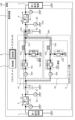
- FIG. 1 is a block diagram showing the configuration of a power supply device according to an embodiment.
- FIG. 2 is a diagram showing a specific circuit example of the DC-DC converter included in the power supply device shown in FIG.
- FIG. 3A is a diagram showing the flow of current in the step-down operation mode of the power supply device shown in FIG. 2.
- FIG. 3B is a diagram illustrating a failure of a switching element in the step-down operation mode of the power supply device shown in FIG. 3A.
- FIG. 3C is a timing chart showing the operation of the first DC/DC converter to explain the open failure of the second switching element.
- FIG. 4A is a diagram showing the flow of current in the boost operation mode of the power supply device shown in FIG. 2.
- FIG. 4B is a diagram illustrating a failure of a switching element in the boost operation mode of the power supply device shown in FIG. 4A.
- FIG. 4C is a timing chart showing the operation of the first DC/DC converter to explain the open failure of the first switching element.
- FIG. 5A is a flowchart showing a method for diagnosing a switch in the power supply device shown in FIG. 2.
- FIG. 5B is a diagram showing the flow of current in the flowchart of FIG. 5A.
- FIG. 5C is a diagram illustrating a modified example of the current flow in diagnosis of the switch in the power supply device illustrated in FIG. 2.
- FIG. 6A is a flowchart showing a method for detecting failure of a switching element in the buck-boost operation mode of the power supply device shown in FIG. 2.
- FIG. 6B is a diagram illustrating the basis of the determination in the flowchart of FIG. 6A.
- FIG. 6C shows a switching element failure detection method in the buck-boost operation mode of the power supply device shown in FIG. 2, in which the step-down and step-up operations of the first DCDC converter and the second DCDC converter in the buck-boost operation mode shown in FIG. 6A are switched. It is a flowchart which shows.
- FIG. 6D is a diagram illustrating the basis of the determination in the flowchart of FIG. 6C.
- FIG. 7 is a block diagram showing the configuration of a power supply device according to Modification 1 of the embodiment.
- FIG. 8 is a block diagram showing the configuration of a power supply device according to a second modification of the embodiment.
- FIG. 9 is a block diagram showing the configuration of a power supply device according to modification 3 of the embodiment.
- FIG. 1 is a block diagram showing the configuration of a power supply device 1 according to an embodiment.
- the power supply device 1 is a power supply installed in a vehicle 100 and connected to a first DC power supply 2 that supplies and holds a first voltage and a second DC power supply 3 that supplies and holds a second voltage lower than the first voltage.
- the device includes a first switch 5 having one end connected to the first DC power supply 2, and a first capacitor 91 connected between the other end of the first switch 5 and a reference potential GND (ground). , a second switch 6 whose one end is connected to the second DC power supply 3, a second capacitor 92 connected between the other end of the second switch 6 and the reference potential GND, and the other end of the first switch 5.
- a DCDC converter section 4 having a first DCDC converter 41 and a second DCDC converter 42 connected in parallel between one end of the second switch 6 and the other end of the second switch 6; and a control section 7 having a diagnosis section 8.
- the power supply device 1 further includes a first potential detection section 51 that detects the voltage at one end of the first switch 5, a second potential detection section 52 that detects the voltage at the other end of the first switch 5, and one end of the second switch 6.
- a third potential detection section 61 that detects the voltage at the other end of the second switch 6 and a fourth potential detection section 62 that detects the voltage at the other end of the second switch 6 are provided.
- the first DC power supply 2 is, for example, a chargeable and dischargeable battery.
- the second DC power source 3 is, for example, a chargeable and dischargeable electric double layer capacitor or a battery.
- the first switch 5 and the second switch 6 are switches that selectively take on and off states, and are, for example, semiconductor switches such as MOSFETs (metal oxide film field effect transistors), or electromagnetic relays. It is a contactor.
- MOSFETs metal oxide film field effect transistors
- electromagnetic relays It is a contactor.
- the first DC/DC converter 41 performs a step-down operation in which the first voltage supplied from the first DC power supply 2 side is stepped down to a second voltage and outputted to the second DC power supply 3 side according to instructions from the control unit 7; A step-up operation is performed in which the second voltage supplied from the DC power source 3 side is boosted to the first voltage and outputted to the first DC power source 2 side.
- the second DC/DC converter 42 performs a step-down operation in which the first voltage supplied from the first DC power supply 2 side is stepped down to a second voltage and outputted to the second DC power supply 3 side according to instructions from the control unit 7; A step-up operation is performed in which the second voltage supplied from the DC power source 3 side is boosted to the first voltage and outputted to the first DC power source 2 side.
- the first potential detection section 51, the second potential detection section 52, the third potential detection section 61, and the fourth potential detection section 62 are, for example, A/D converters.
- the first potential detection section 51 and the second potential detection section 52 constitute a first potential difference detection section that detects the potential difference V5 between both ends of the first switch 5.
- the third potential detection section 61 and the fourth potential detection section 62 constitute a second potential difference detection section that detects the potential difference V6 between both ends of the second switch 6.
- the control unit 7 has the following three operation modes by controlling the first switch 5, the second switch 6, and the DCDC converter unit 4.
- the first DC power supply 2 supplies power to the first DC/DC converter 41 and the second DC/DC converter 42 in parallel, that is, at the same time, with the first switch 5 and the second switch 6 connected.
- This is a step-down operation mode in which step-down control is performed to step down the first voltage to a second voltage and output it to the second DC power supply 3.
- the first DC/DC converter 41 and the second DC/DC converter 42 are supplied with the second
- boost operation mode in which boost control is performed to boost two voltages to a first voltage and output it to the first DC power supply 2.
- the voltage of the first capacitor 91 is reduced to the first DC/DC converter 41 and output to the second capacitor 92.
- This is a buck-boost operation mode in which the second DCDC converter 42 boosts the voltage of the second capacitor 92 and outputs it to the first capacitor 91 in parallel.
- the buck operation and boost operation of the first DC/DC converter 41 and the second DC/DC converter 42 may be switched.
- the voltage of the second capacitor 92 is boosted to the first DCDC converter 41 and outputted to the first capacitor 91, and in parallel
- step-up/down control may be performed on the second DCDC converter 42 to step down the voltage of the first capacitor 91 and output it to the second capacitor 92.
- the step-down operation mode is one of the voltage conversion operations in which the first voltage supplied from the first DC power supply 2 is stepped down and converted into a second voltage to charge the first DC power supply 2.
- the boost operation mode is one of the voltage conversion operations in which the second voltage supplied from the second DC power supply 3 is boosted and converted into a first voltage to charge the first DC power supply 2 .
- the buck-boost operation mode is an operation mode used for diagnosing the breaking abilities of the first switch 5 and the second switch 6 and for fault diagnosis of the switching elements included in the DC/DC converter section 4, and is also referred to as a diagnosis mode.
- the diagnostic section 8 detects the voltage detected by the first potential detection section 51 and the second potential detection section 52 in order to detect the potential difference V5 between both ends of the first switch 5 after the step-up/down control.
- a first potential difference V5 which is the difference between the voltages detected in If the first potential difference V5 is larger than the first reference potential difference, it is determined that the breaking ability of the first switch 5 is normal, and if not, it is determined that the breaking ability of the first switch 5 is abnormal.
- the diagnostic section 8 detects the voltage detected by the third potential detection section 61 and the fourth potential in order to detect the potential difference V6 across the second switch 6 after the buck-boost control. From the voltage detected by the detection unit 62, a second potential difference V6, which is the difference between them, is calculated as a potential difference V6 between both ends of the second switch 6, and the calculated second potential difference V6 is higher than a predetermined second reference potential difference. If the second potential difference V6 is larger than the second reference potential difference, the breaking ability of the second switch 6 is determined to be normal, and if not, the breaking ability of the second switch 6 is determined to be abnormal. judge.
- the control unit 7 and the diagnosis unit 8 are realized by a memory that stores a program, a processor that executes the program, an A/D converter, a timer, and the like.
- first potential difference detection section 51 and the second potential detection section 52 a first potential difference detection section that directly detects the potential difference V5 between both ends of the first switch 5 may be provided.
- second potential difference detection section that directly detects the potential difference V6 between both ends of the second switch 6 may be provided.
- FIG. 2 is a diagram showing a specific circuit example of the DCDC converter section 4 included in the power supply device 1 shown in FIG. 1. Here, a circuit diagram of the entire power supply device 1 including a specific circuit of the DCDC converter unit 4 is shown.
- the first DC/DC converter 41 includes a first current sensor 414, a first switching element 411, and a first reactor 413, which are connected in series between the first switch 5 and the second switch 6.
- 1 reactor 413 has a second switching element 412 connected between a connection point J41 and a reference potential GND, which are connected in series with each other.
- the second DC/DC converter 42 includes a second current sensor 424, a third switching element 421, and a second reactor 423, which are connected in series between the first switch 5 and the second switch 6.
- the second reactor 423 has a fourth switching element 422 connected between the connection point J42 and the reference potential GND, which are connected in series with each other.
- the first current sensor 414 and the second current sensor 424 are sensors that detect the current flowing through the first DCDC converter 41 and the second DCDC converter 42, respectively, and, for example, convert a resistive element and the voltage across the resistive element into a digital value. It consists of an A/D converter, etc.
- the first switching element 411, the second switching element 412, the third switching element 421, and the fourth switching element 422 are all, for example, N-channel MOSFETs and have body diodes. Further, the body diode has an anode on the source electrode side of the switching element and a cathode on the drain electrode side.
- FIG. 3A is a diagram showing the flow of current in the step-down operation mode of the power supply device 1 shown in FIG. 2.
- the first switch 5 and the second switch 6 maintain the connected state, and the first DCDC converter 41 and the second DCDC converter 42 perform the next operation in parallel. I will do it.
- the first switching element 411 is turned on and the second switching element 412 is turned off, so that the current supplied from the first DC power supply 2 is transferred to the first switch as shown in the current path 21a. 5.
- the first switching element 411 is turned off and the second switching element 412 is turned on, whereby the energy stored in the first reactor 413 is released as shown in the current path 21b, and the reference potential GND is Current flows to the second DC power supply 3 via the second switching element 412, the first reactor 413, and the second switch 6, and further, depending on the output mode (high output/low output), the current flows in the opposite path. Current flows.
- the first DCDC converter 41 the above state in which energy is accumulated in the first reactor 413 and the above state in which the energy accumulated in the first reactor 413 is released are alternately and repeatedly switched.
- control unit 7 monitors the current value detected by the first current sensor 414, and controls the first switching element so that the current value is below a predetermined upper limit value or within a predetermined range.
- the switching operation of the first switching element 411 and the second switching element 412 is controlled by controlling the on-duty of a PWM (pulse width modulation) control signal output to the switching element 411 and the second switching element 412.
- the third switching element 421 is turned on and the fourth switching element 422 is turned off, so that the current supplied from the first DC power supply 2 is transferred to the first switch as shown in the current path 22a. 5, the energy flows to the second DC power supply 3 via the second current sensor 424, the third switching element 421, the second reactor 423, and the second switch 6, and as a result, energy is stored in the second reactor 423. Further, the third switching element 421 is turned off, and the fourth switching element 422 is turned on, thereby releasing the energy stored in the second reactor 423, as shown in the current path 22b, and changing the reference potential GND.
- control unit 7 monitors the current value detected by the second current sensor 424, and controls the third switching element so that the current value is below a predetermined upper limit or within a predetermined range.
- the switching operation of the third switching element 421 and the fourth switching element 422 is controlled by controlling the on-duty of the PWM control signal output to the fourth switching element 421 and the fourth switching element 422.
- the first DC/DC converter 41 and the second DC/DC converter 42 step down the first voltage supplied from the first DC power supply 2 to the second voltage and supply the voltage to the second DC power supply 3 in parallel. Perform step-down operation to output.
- FIG. 3B is a diagram illustrating a failure of a switching element in the step-down operation mode of the power supply device 1 shown in FIG. 3A.
- This figure shows the flow of current when the second switching element 412 has an open failure.
- An open failure of a switching element refers to a failure in which a switching element remains cut off and is not connected.
- the current flows from the reference potential GND through the second switching element 412 toward the first reactor 413.
- the current that flows is a current that flows in the forward direction of the body diode through the body diode of the second switching element 412, and no current flows in the opposite direction, resulting in asynchronous rectification.
- FIG. 3C is a timing chart showing the operation of the first DC/DC converter 41 to explain the open failure of the second switching element 412.
- Hi-Side switch (411) indicates on/off of the first switching element 411
- Lo-Side switch (412) indicates on/off of the second switching element 412
- Inductor (413) indicates on/off of the second switching element 412.
- “Inductor (413) current: at low output (synchronous rectification: continuous mode)” indicates the current flowing through the second switching element at low output.
- This phenomenon also occurs when the fourth switching element 422 in the second DCDC converter 42 has an open failure.
- the step-down operation mode even if the switching elements on the Lo side in each DCDC converter, that is, the second switching element 412 and the fourth switching element 422, have an open failure, the step-down operation is performed, so the failure can be discovered. It is difficult to do so. On the other hand, as will be described later, in the diagnostic mode, an open failure of the switching element can be detected.
- FIG. 4A is a diagram showing the flow of current in the boost operation mode of the power supply device 1 shown in FIG. 2.
- the first switch 5 and the second switch 6 maintain the connected state, and the first DCDC converter 41 and the second DCDC converter 42 perform the next operation in parallel. In other words, do it at the same time.
- the first switching element 411 is turned off and the second switching element 412 is turned on, so that the current supplied from the second DC power supply 3 is transferred to the first reactor as shown in the current path 31a. 413 and the second switching element 412 to the reference potential GND, and as a result, energy is stored in the first reactor 413. Further, the first switching element 411 is turned on and the second switching element 412 is turned off, whereby the energy stored in the first reactor 413 is released as shown in the current path 31b, and the second DC power supply 3 flows into the first DC power supply 2 via the first reactor 413 , the first switching element 411 , the first current sensor 414 , and the first switch 5 .
- the above state in which energy is accumulated in the first reactor 413. The above state in which the energy stored in the first reactor 413 is released is alternately and repeatedly switched.
- control unit 7 monitors the current value detected by the first current sensor 414, and controls the first switching element so that the current value is below a predetermined upper limit value or within a predetermined range.
- the switching operation of the first switching element 411 and the second switching element 412 is controlled by controlling the on-duty of the PWM control signal output to the first switching element 411 and the second switching element 412.
- the third switching element 421 is turned off and the fourth switching element 422 is turned on, whereby the current supplied from the second DC power supply 3 is transferred to the second reactor as shown in the current path 32a. 423 and the fourth switching element 422 to the reference potential GND, and as a result, energy is stored in the second reactor 423. Further, the third switching element 421 is turned on and the fourth switching element 422 is turned off, whereby the energy stored in the second reactor 423 is released as shown in the current path 32b, and the second DC power supply Current flows from DC power supply 3 to first DC power supply 2 via second reactor 423 , third switching element 421 , second current sensor 424 , and first switch 5 .
- the above state in which energy is accumulated in the second reactor 423. The above state in which the energy stored in the second reactor 423 is released is alternately and repeatedly switched.
- control unit 7 monitors the current value detected by the second current sensor 424, and controls the third switching element so that the current value is below a predetermined upper limit or within a predetermined range.
- the switching operation of the third switching element 421 and the fourth switching element 422 is controlled by controlling the on-duty of the PWM control signal output to the fourth switching element 421 and the fourth switching element 422.
- the first DC/DC converter 41 and the second DC/DC converter 42 boost the second voltage supplied from the second DC power supply 3 to the first voltage in parallel, and supply the second voltage to the first DC power supply 2. Performs boost operation to output.
- FIG. 4B is a diagram illustrating a failure of a switching element in the boost operation mode of the power supply device 1 shown in FIG. 4A. This figure shows the flow of current when the first switching element 411 has an open failure. As shown in this figure, when the first switching element 411 has an open failure, the current flowing from the first reactor 413 to the first current sensor 414 is The current flows through the body diode of the switching element 411 in the forward direction of the body diode.
- FIG. 4C is a timing chart showing the operation of the first DC/DC converter 41 to explain the open failure of the first switching element 411.
- “Lo-Side switch (412)” indicates on/off of the second switching element 412
- “Hi-Side switch (411)” indicates on/off of the first switching element 411
- “Inductor (413)” indicates on/off of the first switching element 411.
- )Current: At high output” indicates the current flowing through the first reactor 413 at high output
- “Inductor (413) current: at low output (synchronous rectification: continuous mode)” indicates the current flowing through the first switching element at low output.
- This phenomenon also occurs when the third switching element 421 in the second DCDC converter 42 has an open failure.
- the boost operation mode even if the Hi-side switching elements in each DCDC converter, that is, the first switching element 411 and the third switching element 421, have an open failure, the boost operation is performed, so the failure can be discovered. It is difficult to do so. On the other hand, as will be described later, in the diagnostic mode, an open failure of the switching element can be detected.
- FIG. 5A is a flowchart showing a method for diagnosing the switches 5 and 6 in the power supply device 1 shown in FIG. 2.
- control unit 7 instructs the first switch 5 and the second switch 6 to turn off the first switch 5 and the second switch 6 (S10).
- the control unit 7 causes the DC/DC converter unit 4 to perform step-up/down operation to release the charges accumulated in the first capacitor 91 and the charges accumulated in the second capacitor 92 ( S11). Specifically, the control unit 7 causes the first DC/DC converter 41 to perform a step-down operation for a certain period of time (for example, one second), and in parallel, that is, at the same time, causes the second DC/DC converter 42 to perform a step-up operation. The charges accumulated in the capacitance 91 and the second capacitance 92 are released.
- FIG. 5B is a diagram showing the flow of current in step S11 of FIG. 5A.
- the first switching element 411 is turned on and the second switching element 412 is turned off, thereby releasing the charge accumulated in the first capacitance 91 as shown in the current path 21a. Then, a current flows to the second capacitance 92 via the first current sensor 414, the first switching element 411, and the first reactor 413, and as a result, energy is stored in the first reactor 413.
- the first switching element 411 is turned off and the second switching element 412 is turned on, whereby the energy stored in the first reactor 413 is released as shown in the current path 21b, and the reference potential GND is A current flows to the second capacitor 92 via the second switching element 412 and the first reactor 413, and further, depending on the output mode (high output/low output), the current flows in the opposite path.
- the first DCDC converter 41 the above state in which energy is accumulated in the first reactor 413 and the above state in which the energy accumulated in the first reactor 413 is released are alternately and repeatedly switched.
- the charge accumulated in the first capacitor 91 is released, and the voltage of the first capacitor 91 decreases.
- the third switching element 421 is turned off and the fourth switching element 422 is turned on, thereby releasing the charge accumulated in the second capacitance 92, as shown in the current path 32a. Then, a current flows to the reference potential GND via the second reactor 423 and the fourth switching element 422, and as a result, energy is accumulated in the second reactor 423. Further, the third switching element 421 is turned on and the fourth switching element 422 is turned off, whereby the energy stored in the second reactor 423 is released as shown in the current path 32b, and the second electrostatic Current flows from the capacitor 92 to the first capacitor 91 via the second reactor 423, the third switching element 421, and the second current sensor 424. In the second DCDC converter 42, the above state in which energy is accumulated in the second reactor 423. The above state in which the energy stored in the second reactor 423 is released is alternately and repeatedly switched.
- the second capacitance 92 is charged by the first DCDC converter 41, and the first capacitance 91 is charged by the second DCDC converter 42.
- the conversion efficiency in the first DCDC converter 41 and the second DCDC converter 42 will never exceed 100%.
- the energy of the first capacitance 91 and the second capacitance 92 is Since the sum decreases due to the loss of the first DCDC converter 41 and the second DCDC converter 42, the voltage of both the first capacitance 91 and the second capacitance 92 decreases.
- the diagnostic unit 8 of the control unit 7 detects the voltage detected by the first potential detection unit 51 and the voltage detected by the second potential detection unit 52 in order to detect the potential difference V5 between both ends of the first switch 5.
- a first potential difference V5, which is the difference between them, is calculated (S12), and it is determined whether the calculated first potential difference V5 is larger than a predetermined first reference potential difference (S13), and the first potential difference V5 is If it is larger than the first reference potential difference (Yes in S13), it is determined that the interrupting ability of the first switch 5 is normal (S14), and if the first potential difference V5 is not larger than the first reference potential difference, (No in S13), it is determined that the breaking ability of the first switch 5 is abnormal (S15).
- the diagnostic unit 8 of the control unit 7 uses the voltage detected by the third potential detection unit 61 and the voltage detected by the fourth potential detection unit 62 in order to detect the potential difference V6 between both ends of the second switch 6.
- a second potential difference V6, which is the difference between them, is calculated (S16), and it is determined whether the calculated second potential difference V6 is larger than a predetermined second reference potential difference (S17). is larger than the second reference potential difference (Yes in S17), it is determined that the interrupting ability of the second switch 6 is normal (S18), and if the second potential difference V6 is not larger than the second reference potential difference, (No in S17), it is determined that the interrupting ability of the second switch 6 is abnormal (S19).
- the first static The charge accumulated in the capacitance 91 is released and the voltage of the first capacitance 91 falls, and at the same time, the charge accumulated in the second capacitance 92 is released due to the step-up operation by the second DCDC converter 42. As a result, the voltage of the second capacitor 92 decreases.
- the interrupting ability of the first switch 5 when the interrupting ability of the first switch 5 is normal, the potential difference V5 between both ends of the first switch 5 is reduced. becomes large in a short time, and similarly, when the breaking ability of the second switch 6 is normal, the potential difference V6 between both ends of the second switch 6 becomes large in a short time.
- the interrupting abilities of the first switch 5 and the second switch 6 can be diagnosed in a shorter time than in the power supply device of the comparative example and at the same time.
- the diagnosis of the second switch 6 in steps S16 to S19 may be performed before the diagnosis of the first switch 5 in steps S12 to S15.
- the control unit 7 monitors the voltage detected by the second potential detection unit 52 to detect the first electrostatic potential.
- the first DCDC converter 41 and the second DCDC converter 42 perform step-up operation to charge the first capacitor 91, and the potential difference V5 between both ends of the first switch 5 is increased.
- the first switch 5 may be turned on after the value falls within a predetermined range. This suppresses the generation of rush current caused by changing the first switch 5 from the disconnected state to the connected state in a state where the potential difference V5 between both ends is large.
- the control unit 7 monitors the voltage detected by the fourth potential detection unit 62, thereby controlling the second capacitance 92.
- the second capacitor 92 is charged by causing the first DC/DC converter 41 and the second DC/DC converter 42 to perform step-down operation so that the voltage approaches the original second voltage, and the potential difference V6 across the second switch 6 is set to a predetermined value.
- the second switch 6 may be placed in the connected state after the distance is within the range. This suppresses the generation of rush current caused by changing the second switch 6 from the disconnected state to the connected state in a state where the potential difference V6 between both ends is large.
- FIG. 5C is a diagram showing a modification example of the current flow in diagnosis of the switch in the power supply device 1 shown in FIG. 2.
- the control unit 7 keeps the second switching element 412 and the third switching element 421 off at all times (hereinafter, this state is also referred to as "fixed open"), and controls the buck-boost operation mode. Take control.
- the first switching element 411 is turned on while the second switching element 412 is maintained off, and thereby the current shown in the current path 21a is turned on. As shown in FIG. As a result, energy is accumulated in the first reactor 413. Further, in the first DCDC converter 41, under the control of the control unit 7, the first switching element 411 is turned off while the second switching element 412 is maintained off, and thereby, as shown in the current path 21b, The energy stored in the first reactor 413 is released, and a current flows from the reference potential GND to the second capacitor 92 via the body diode of the second switching element 412 and the first reactor 413.
- the above state in which the energy is released is alternately and repeatedly switched.
- the charge accumulated in the first capacitor 91 is released, and the voltage of the first capacitor 91 decreases.
- the fourth switching element 422 is turned on while the third switching element 421 is maintained off, and thereby, as shown in the current path 32a, the fourth switching element 422 is turned on. , the charge accumulated in the second capacitance 92 is released, a current flows to the reference potential GND via the second reactor 423 and the fourth switching element 422, and as a result, energy is accumulated in the second reactor 423. be done.
- the fourth switching element 422 is turned off while the third switching element 421 is maintained off, and thereby, as shown in the current path 32b,
- the energy stored in the second reactor 423 is released and is transferred from the second capacitor 92 to the first capacitor 91 via the second reactor 423, the body diode of the third switching element 421, and the second current sensor 424. Current flows.
- the above state in which energy is accumulated in the second reactor 423 while the third switching element 421 remains off, and the state in which energy is accumulated in the second reactor 423, The above state in which the energy is released is alternately and repeatedly switched.
- FIG. 6A is a flowchart showing a method for detecting a failure of a switching element in the buck-boost operation mode of the power supply device 1 shown in FIG. 2.
- control unit 7 turns off the first switch 5 and the second switch 6 (S20).
- the control unit 7 causes the DC/DC converter unit 4 to perform a step-up/down operation to release the charges accumulated in the first capacitor 91 and the second capacitor 92 (S21). Specifically, the control unit 7 causes the first DC/DC converter 41 to perform a step-down operation for a certain period of time (for example, 1 second), and in parallel causes the second DC/DC converter 42 to perform a step-up operation, thereby reducing the first electrostatic charge. The charges accumulated in the capacitor 91 and the charges accumulated in the second capacitor 92 are discharged.
- the control unit 7 detects the first potential P15 with the second potential detection unit 52 (S22), and determines whether the first potential P15 detected by the second potential detection unit 52 is equal to or lower than a predetermined first reference potential. If the first potential P15 is equal to or lower than the first reference potential (Yes in S23), it is determined that the first switching element 411 is normal (S24); is not equal to or lower than the first reference potential (No in S23), it is determined that the first switching element 411 is in an abnormal state (open failure) where it is fixed to OFF (S25).
- the control unit 7 detects the second potential P16 with the fourth potential detection unit 62 (S36), and determines that the second potential P16 detected by the fourth potential detection unit 62 is equal to or lower than a predetermined second reference potential. (S27), and if the second potential P16 is equal to or lower than the second reference potential (Yes in S27), it is determined that the fourth switching element 422 is normal (S28); If P16 is not equal to or lower than the second reference potential (No in S27), it is determined that the fourth switching element 422 is in an abnormal state (open failure) where it is fixed in an off state (S29).
- FIG. 6B is a diagram illustrating the basis for the determinations in steps S23 to S25 in FIG. 6A and the determinations in steps S27 to S29 in FIG. 6A.
- the difference in current flow when the first switching element 411 and the fourth switching element 422 have an open failure is shown based on FIG. 5C.
- the first switching element 411 when the first switching element 411 is normal, the first switching element 411 is turned on as shown in the current path 21a, and thereby the first switching element 411 is turned on, thereby reducing the amount of electricity accumulated in the first capacitance 91. The accumulated charge is released, and a current flows to the second capacitor 92 via the first current sensor 414, the first switching element 411, and the first reactor 413, and as a result, energy is stored in the first reactor 413. . Further, in the first DC/DC converter 41, when the first switching element 411 is normal, the first switching element 411 is turned off as shown in the current path 21b, and thereby the accumulation in the first reactor 413 is reduced.
- the energy is released, and a current flows from the reference potential GND to the second capacitor 92 via the body diode of the second switching element 412 and the first reactor 413.
- the first DC/DC converter 41 when the first switching element 411 is normal, the above state in which energy is accumulated in the first reactor 413 and the above state in which the energy accumulated in the first reactor 413 is released. can be alternately and repeatedly switched.
- the step-down operation by the first DCDC converter 41 due to the step-down operation by the first DCDC converter 41, the charge accumulated in the first capacitor 91 is released, and the voltage of the first capacitor 91 decreases.
- the first switching element 411 has an open failure, no current flows in the direction from the first capacitance 91 to the first reactor 413 via the first switching element 411. Therefore, the step-down operation by the first DCDC converter 41 is not performed, and the charge accumulated in the first capacitor 91 is not sufficiently released, and the voltage of the first capacitor 91, that is, the second potential detection unit The first potential P15 detected at 52 does not fall sufficiently, or it takes time for it to fall sufficiently.
- control unit 7 determines that the first switching element 411 has an open failure when the first potential P15 detected by the second potential detection unit 52 is not lower than or equal to the first reference potential (No in S23). Yes, it is possible (S25).
- the fourth switching element 422 when the fourth switching element 422 is normal, the fourth switching element 422 is turned on as shown in the current path 32a, and thereby the second capacitance 92 is The accumulated charge is released, and a current flows to the reference potential GND via the second reactor 423 and the fourth switching element 422, and as a result, energy is accumulated in the second reactor 423.
- the fourth switching element 422 when the fourth switching element 422 is normal, the fourth switching element 422 is turned off as shown in the current path 32b, and thereby the accumulation in the second reactor 423 is stopped.
- the energy is released, and a current flows from the second capacitance 92 to the first capacitance 91 via the second reactor 423, the body diode of the third switching element 421, and the second current sensor 424.
- the fourth switching element 422 when the fourth switching element 422 is normal, the above state in which energy is accumulated in the second reactor 423 and the above state in which the energy accumulated in the second reactor 423 is released. can be alternately and repeatedly switched.
- the boost operation by the second DCDC converter 42 is not performed, and the charge accumulated in the second capacitance 92 is not sufficiently released, and the second capacitance 92, that is, the fourth potential detection unit 62 The detected second potential P16 does not fall sufficiently, or it takes time to fall sufficiently.
- control unit 7 determines that the fourth switching element 422 has an open failure when the second potential P16 detected by the fourth potential detection unit 62 is not equal to or lower than the second reference potential (No in S27). Yes, it is possible (S29).
- the buck-boost operation mode diagnosis mode
- the buck operation and boost operation of the first DCDC converter 41 and the second DCDC converter 42 may be switched.
- the voltage of the second capacitor 92 is boosted to the first DCDC converter 41 and outputted to the first capacitor 91, and in parallel
- step-up/down control may be performed on the second DCDC converter 42 to step down the voltage of the first capacitor 91 and output it to the second capacitor 92.
- FIG. 6C shows the switching elements in the buck-boost operation mode of the power supply device 1 shown in FIG. 2, in which the step-down and step-up operations of the first DCDC converter 41 and the second DCDC converter 42 in the buck-boost operation mode shown in FIG. 6A are switched.
- 3 is a flowchart showing a failure detection method.
- control unit 7 turns off the first switch 5 and the second switch 6 (S30).
- the control unit 7 causes the DC/DC converter unit 4 to perform a step-up/down operation to release the charges accumulated in the first capacitance 91 and the second capacitance 92 (S31). Specifically, the control unit 7 causes the first DC/DC converter 41 to perform a step-up operation for a certain period of time (for example, 1 second), and in parallel causes the second DC/DC converter 42 to perform a step-down operation, thereby reducing the first electrostatic charge. The charges accumulated in the capacitor 91 and the charges accumulated in the second capacitor 92 are discharged.
- the control unit 7 inspects the first potential P15 using the second potential detection unit 52 (S32), and determines whether the first potential P15 detected by the second potential detection unit 52 is equal to or lower than a predetermined first reference potential. If the first potential P15 is equal to or lower than the first reference potential (S33: Yes), it is determined that the third switching element 421 is normal (S34); is not equal to or lower than the first reference potential (No in S33), it is determined that the third switching element 421 is in an abnormal state (open failure) where it is fixed in an off state (S35).
- the control unit 7 detects the second potential P16 with the fourth potential detection unit 62 (S36), and determines that the second potential P16 detected by the fourth potential detection unit 62 is equal to or lower than a predetermined second reference potential. (S37), and if the second potential P16 is equal to or lower than the second reference potential (Yes in S37), it is determined that the second switching element 412 is normal (S38); If P16 is not equal to or lower than the second reference potential (No in S37), it is determined that the second switching element 412 is in an abnormal state (open failure) where it is fixed in the OFF state (S39).
- FIG. 6D is a diagram illustrating the basis for the determinations in steps S33 to S35 in FIG. 6C and the determinations in steps S37 to S39 in FIG. 6C.
- the difference in current flow when the second switching element 412 and the third switching element 421 have an open failure is shown based on FIG. 5C.
- the third switching element 421 when the third switching element 421 is normal, the third switching element 421 is turned on as shown in the current path 22a, and thereby the capacitance accumulated in the first capacitance 91 is reduced. The accumulated charge is released, and a current flows to the second capacitor 92 via the second current sensor 424, the third switching element 421, and the second reactor 423, and as a result, energy is stored in the second reactor 423. .
- the third switching element 421 when the third switching element 421 is normal, the third switching element 421 is turned off as shown in the current path 22b, and thereby the accumulation in the second reactor 423 is reduced.
- the energy is released, and a current flows from the reference potential GND to the second capacitor 92 via the body diode of the fourth switching element 422 and the second reactor 423.
- the third switching element 421 when the third switching element 421 is normal, the above state in which energy is accumulated in the second reactor 423 and the above state in which the energy accumulated in the second reactor 423 is released. can be alternately and repeatedly switched.
- the charges accumulated in the first capacitor 91 are released, and the voltage of the first capacitor 91 decreases.
- the third switching element 421 has an open failure, no current flows in the direction from the first capacitance 91 to the second reactor 423 via the third switching element 421. Therefore, the step-down operation by the second DCDC converter 42 is not performed, and the charges accumulated in the first capacitor 91 are not sufficiently released, and the voltage of the first capacitor 91, that is, the second potential detection unit The first potential P15 detected at 52 does not fall sufficiently, or it takes time for it to fall sufficiently.
- control unit 7 determines that the third switching element 421 has an open failure when the first potential P15 detected by the second potential detection unit 52 is not lower than or equal to the first reference potential (No in S33). Yes, it is possible (S35).
- the second switching element 412 when the second switching element 412 is normal, the second switching element 412 is turned on as shown in the current path 31a, and thereby the second capacitance 92 is The accumulated charge is released, and a current flows to the reference potential GND via the first reactor 413 and the second switching element 412, and as a result, energy is accumulated in the first reactor 413. Further, in the first DC/DC converter 41, when the second switching element 412 is normal, the second switching element 412 is turned off as shown in the current path 31b, and thereby the accumulation in the first reactor 413 is reduced.
- the energy is released, and a current flows from the second capacitance 92 to the first capacitance 91 via the first reactor 413, the body diode of the first switching element 411, and the first current sensor 414.
- the first DC/DC converter 41 when the second switching element 412 is normal, the above state in which energy is accumulated in the first reactor 413 and the above state in which the energy accumulated in the first reactor 413 is released. can be alternately and repeatedly switched.
- the charges accumulated in the second capacitor 92 are released, and the voltage of the second capacitor 92 decreases.
- the second switching element 412 has an open failure, no current flows in the direction from the second capacitance 92 toward the reference potential GND via the first reactor 413 and the second switching element 412. Therefore, the step-up operation by the first DCDC converter 41 is not performed, and the charges accumulated in the second capacitance 92 are not sufficiently released, and the second capacitance 92, that is, the fourth potential detection unit 62 The detected second potential P16 does not fall sufficiently, or it takes time to fall sufficiently.
- control unit 7 determines that the second switching element 412 has an open failure when the second potential P16 detected by the fourth potential detection unit 62 is not equal to or lower than the second reference potential (No in S37). Yes, it is possible (S39).
- the buck-boost operation mode diagnosis mode
- the power supply device 1 includes the first DC power supply 2 that supplies and holds the first voltage, and the second DC power supply 3 that supplies and holds the second voltage lower than the first voltage.
- a power supply device connected to a first switch 5, one end of which is connected to the first DC power supply 2, and a first capacitor connected between the other end of the first switch 5 and a reference potential GND.
- a second switch 6 whose one end is connected to the second DC power supply 3, a second capacitor 92 connected between the other end of the second switch 6 and the reference potential GND, and the first switch 5.
- a DCDC converter section 4 having a first DCDC converter 41 and a second DCDC converter 42 connected in parallel between the other end and the other end of the second switch 6, the first switch 5, the second switch 6, and the DCDC converter.
- the control unit 7 controls the first DCDC converter 41 and the second DCDC converter 42 in parallel with the first switch 5 and the second switch 6 connected.
- the first switch 5 and the second switch 6 are connected to a step-down operation mode in which step-down control is performed to step down the first voltage supplied from the first DC power supply 2 to a second voltage and output it to the second DC power supply 3.
- step-up control for the first DC/DC converter 41 and the second DC/DC converter 42 to step up the second voltage supplied from the second DC power supply 3 to the first voltage and output it to the first DC power supply 2 in parallel.
- the voltage of the first capacitor 91 is stepped down for the first DC/DC converter 41 and output to the second capacitor 92.
- buck-boost operation mode diagnosis mode
- buck-boost control is performed for the second DCDC converter 42 to boost the voltage of the second capacitor 92 and output it to the first capacitor 91.
- the first DCDC converter 41 steps down the voltage of the first capacitor 91 and outputs it to the second capacitor 92 while the first switch 5 and the second switch 6 are cut off.
- the second DCDC converter 42 boosts the voltage of the second capacitor 92 and outputs it to the first capacitor 91. Therefore, when the breaking ability of the first switch 5 is normal, the potential difference V5 between both ends of the first switch 5 increases in a short time, and when the breaking ability of the second switch 6 is normal, the potential difference V5 across the first switch 5 becomes large. The potential difference V6 between both ends becomes large in a short time. As a result, the breaking abilities of the first switch 5 and the second switch 6 can be diagnosed in a shorter time than in the past and at the same time.
- the power supply device 1 includes a first potential difference detection section that detects a potential difference V5 between both ends of the first switch 5, and a second potential difference detection section that detects a potential difference V6 between both ends of the second switch 6.
- the control section 7 determines whether the first potential difference V5 detected by the first potential difference detection section is larger than the first reference potential difference after the buck-boost control, and determines whether the first potential difference V5 is larger than the first reference potential difference. If the first potential difference V5 is larger than the first reference potential difference, it is determined that the first switch 5 is normal, and if the first potential difference V5 is not larger than the first reference potential difference, it is determined that the first switch 5 is abnormal and cannot be shut off. .
- the control section 7 determines whether or not the second potential difference V6 detected by the second potential difference detection section is larger than the second reference potential difference after the step-up/down control, and determines whether or not the second potential difference V6 is larger than the second reference potential difference.
- V6 is larger than the second reference potential difference, it is determined that the second switch 6 is normal, and when the second potential difference V6 is not larger than the second reference potential difference, it is determined that the second switch 6 is abnormal and cannot be shut off. Can be judged.
- control unit 7 may perform step-down by the first DCDC converter 41 and step-up by the second DCDC converter 42 for a certain period of time after cutting off the first switch 5 and the second switch 6. . This makes it possible to set the potential difference V6 across the first switch 5 and the second switch 6 to an appropriate value.
- the first DC/DC converter 41 includes a first switching element 411 and a first reactor 413 connected in series between the first switch 5 and the second switch 6;
- the second DCDC converter 42 has a second switching element 412 having a body diode connected between the connection point J41 and the reference potential GND, which are connected in series with each other.
- a third switching element 421 having a body diode and a second reactor 423 are connected in series between the third switching element 421 and the second reactor 423, and a connection point J42 where the third switching element 421 and the second reactor 423 are connected in series with each other and a reference. It may also include a fourth switching element 422 connected between it and the potential GND.
- control section 7 may perform step-up/down control with the second switching element 412 and the third switching element 421 always turned off.
- the control section 7 may perform step-up/down control with the second switching element 412 and the third switching element 421 always turned off.
- the first DCDC converter 41 and the second DCDC converter 42 have a first current sensor 414 and a second current sensor 424 that detect the current flowing through the first DCDC converter 41 and the second DCDC converter 42, and the control unit 7 performs step-down operation. mode, the boost operation mode, and the buck-boost operation mode, the DCDC converter unit 4 may be controlled so that the current detected by the first current sensor 414 and the second current sensor 424 falls within a predetermined range. Thereby, the current flowing through the first DCDC converter 41 and the second DCDC converter 42 is limited to a certain level or less, and the generation of rush current is suppressed.
- the power supply device 1 also includes a second potential detection section 52 that detects the potential P15 at the other end of the first switch 5, and a fourth potential detection section 62 that detects the potential P16 at the other end of the second switch 6.
- the control unit 7 determines whether the first potential P15 detected by the second potential detection unit 52 is lower than or equal to the first reference potential, and determines whether the first potential P15 is equal to or lower than the first reference potential. If it is not below, it is determined that there is an abnormality in which the first switching element 411 is fixed off, and it is determined whether the second potential P16 detected by the fourth potential detection unit 62 is equal to or lower than the second reference potential.
- the second potential P16 is not equal to or lower than the second reference potential, it may be determined that there is an abnormality in which the fourth switching element 422 is fixed off. As a result, the open failure of the first switching element 411 and the fourth switching element 422 is detected simultaneously with the diagnosis of the first switch 5 and the second switch 6.
- the method for diagnosing the power supply device 1 includes a first DC power supply 2 that supplies and holds a first voltage, and a second DC power supply 3 that supplies and holds a second voltage lower than the first voltage.
- the power supply device 1 includes a first switch 5 whose one end is connected to the first DC power supply 2, and a power supply between the other end of the first switch 5 and a reference potential GND.
- a diagnostic method comprising a capacitor 92 and a DCDC converter unit 4 having a first DCDC converter 41 and a second DCDC converter 42 connected in parallel between the other end of the first switch 5 and the other end of the second switch 6. With the first switch 5 and the second switch 6 connected, the first voltage supplied from the first DC power supply 2 is applied to the first DC/DC converter 41 and the second DC/DC converter 42 in parallel.
- the first DCDC converter 41 and the second DCDC converter 42 With the first switch 5 and the second switch 6 connected to the step-down step that performs step-down control to step down the voltage and output it to the second DC power supply 3,
- a boosting step is performed in which the second voltage supplied from the second DC power supply 3 is boosted to the first voltage and is outputted to the first DC power supply 2, and the first switch 5 and the second switch 6 are In the cut-off state, the first DC/DC converter 41 steps down the voltage of the first capacitor 91 and outputs it to the second capacitor 92, and in parallel, the second DC/DC converter 42
- This step includes a step-up/down step (diagnosis mode) in which step-up/down control is performed to step up the voltage of the capacitor 92 and output it to the first capacitor 91 .
- the first DCDC converter 41 steps down the voltage of the first capacitor 91 and outputs it to the second capacitor 92 while the first switch 5 and the second switch 6 are cut off.
- the second DCDC converter 42 boosts the voltage of the second capacitor 92 and outputs it to the first capacitor 91. Therefore, when the breaking ability of the first switch 5 is normal, the potential difference V5 between both ends of the first switch 5 increases in a short time, and when the breaking ability of the second switch 6 is normal, the potential difference V5 across the first switch 5 becomes large. The potential difference V6 between both ends becomes large in a short time. As a result, the breaking abilities of the first switch 5 and the second switch 6 can be diagnosed in a shorter time than in the past and at the same time.
- the step-up/down step after the step-up/down control, it is determined whether the first potential difference V5 detected by the first potential difference detection section is larger than the first reference potential difference, and the first potential difference V5 is determined to be higher than the first reference potential difference. If the first potential difference V5 is larger than the first reference potential difference, it can be determined that the first switch 5 is normal, and if the first potential difference V5 is not larger than the first reference potential difference, it can be determined that the first switch 5 is abnormal and cannot be shut off.
- step-up/down step after the step-up/down control, it is determined whether the second potential difference V6 detected by the second potential difference detection section is larger than the second reference potential difference, and the second potential difference V6 is determined to be the second reference potential difference. If the second potential difference V6 is larger than the second reference potential difference, it can be determined that the second switch 6 is normal, and if the second potential difference V6 is not larger than the second reference potential difference, it can be determined that the second switch 6 is abnormal and cannot be shut off.
- the present disclosure is not limited to the embodiments.
- the scope of the present disclosure also includes various modifications that can be thought of by those skilled in the art to the present embodiment, and other forms constructed by combining some of the constituent elements of the embodiments, as long as they do not depart from the spirit of the present disclosure. contained within.
- the DCDC converter included in the power supply device is not limited to the circuit shown in FIG. 2, but may be another circuit.
- a power supply device according to a modified example including different types of DC/DC converters will be described.
- FIG. 7 is a block diagram showing the configuration of a power supply device 1a according to Modification 1 of the embodiment.
- a power supply device 1a according to this modification has a configuration in which the DCDC converter section 4 in the power supply device 1 according to the embodiment shown in FIG. 2 is replaced with a DCDC converter section 4a according to this modification.
- differences from the embodiment will be mainly explained.
- the DCDC converter section 4a has a first DCDC converter 41a and a second DCDC converter 42a connected in parallel.
- the first DCDC converter 41a includes a fifth switching element 415 connected in series with the first reactor 413, and a fifth switching element 415 and the first reactor 413. It has a sixth switching element 416 connected between the connection point J41a and the reference potential GND, which are connected in series with each other.
- the second DC/DC converter 42a includes a seventh switching element 425 connected in series with the second reactor 423, and a seventh switching element 425 and the second reactor 423.
- the eighth switching element 426 is connected between the connection point J42a and the reference potential GND, which are connected in series with each other.
- the fifth switching element 415, the sixth switching element 416, the seventh switching element 425, and the eighth switching element 426 are all, for example, N-channel MOSFETs and have body diodes. Further, the body diode has an anode on the source electrode side of the switching element and a cathode on the drain electrode side.
- the first DC/DC converter 41a can perform not only a step-down operation but also a step-up operation when charging the second DC power source 3 from the first DC power source 2.
- the fifth switching element 415 is kept on and the sixth switching element 416 is kept off, and operates in the same manner as the DCDC converter section 4 according to the embodiment.
- the first switching element 411 is kept on, the second switching element 412 is kept off, the fifth switching element 415 is turned off, the sixth switching element 416 is turned on, and the first DC A current flows from the power source 2 to the reference potential GND via the first current sensor 414, the first switching element 411, the first reactor 413, and the sixth switching element 416, whereby energy is stored in the first reactor 413.
- the fifth switching element 415 is turned on, the sixth switching element 416 is turned off, and by releasing the energy stored in the first reactor 413, the first DC power supply 2 is turned on, the first current sensor 414, the first switching element 411, A state in which current flows to the second DC power supply 3 via the first reactor 413 and the fifth switching element 415 is alternately repeated.
- the first DC/DC converter 41a can perform not only a step-up operation but also a step-down operation when charging the first DC power source 2 from the second DC power source 3.
- the fifth switching element 415 is kept on and the sixth switching element 416 is kept off, and operates in the same manner as the DCDC converter section 4 according to the embodiment.
- the first switching element 411 remains on, the second switching element 412 remains off, the fifth switching element 415 turns on, the sixth switching element 416 turns off, and the second DC Current flows from the power supply 3 to the first DC power supply 2 via the fifth switching element 415, the first reactor 413, the first switching element 411, and the first current sensor 414, and thereby energy is stored in the first reactor 413.
- the fifth switching element 415 is turned off, the sixth switching element 416 is turned on, and the energy stored in the first reactor 413 is released.
- a state in which current flows to the first DC power supply 2 via the first switching element 411 and the first current sensor 414 is alternately repeated.
- the second DC/DC converter 42a performs not only a step-down operation but also a step-up operation when charging the second DC power source 3 from the first DC power source 2 under the control of the control unit 7. You can also do that. Further, like the first DC/DC converter 41a, when charging the first DC power supply 2 from the second DC power supply 3 under the control of the control unit 7, the second DC/DC converter 42a performs not only a step-up operation but also a step-down operation. You can also do
- control unit 7 operates as follows in the voltage step-down operation mode, voltage-up operation mode, and voltage-up/down operation mode (diagnosis mode). That is, in addition to the operation control in the embodiment, the control unit 7 can perform the following operation control.
- control unit 7 performs the following control.
- control unit 7 supplies power from the second DC power supply 3 to the first DC/DC converter 41 and the second DC/DC converter 42 in parallel with the first switch 5 and the second switch 6 connected. Step-down control is performed to step down the second voltage to the first voltage and output it to the first DC power supply 2.
- control unit 7 controls the first DC power supply 2 in parallel with the first DC/DC converter 41 and the second DC/DC converter 42 with the first switch 5 and the second switch 6 connected.
- Boosting control is performed to boost the first voltage supplied from the DC power source 3 to a second voltage and output it to the second DC power supply 3.
- the control unit 7 steps down the voltage of the second capacitance 92 to the first DC/DC converter 41 with the first switch 5 and the second switch 6 cut off. In parallel, step-up/down control is performed for the second DC/DC converter 42 to step up the voltage of the first capacitor 91 and output it to the second capacitor 92. .
- the control unit 7 causes the first DC/DC converter 41 to boost the voltage of the first capacitor 91 and output it to the second capacitor 92. In parallel with this, step-up/down control is performed on the second DC/DC converter 42 to step down the voltage of the second capacitor 92 and output it to the first capacitor 91.
- the power supply device 1a similarly to the embodiment, in the buck-boost operation mode (diagnosis mode), after the first switch 5 and the second switch 6 are cut off, the first DC/DC converter 41
- the charge stored in the first capacitor 91 is released by the step-down or step-up operation by the second DC/DC converter 42, and the voltage of the first capacitor 91 decreases.
- the charge stored in the capacitor 92 is released, and the voltage of the second capacitor 92 drops.
- the breaking ability of the first switch 5 when the breaking ability of the first switch 5 is normal, the potential difference V5 across the first switch 5 decreases for a short time.
- the second switch 6 has a normal interrupting ability, the potential difference V6 across the second switch 6 becomes large in a short time. Thereby, the breaking abilities of the first switch 5 and the second switch 6 can be diagnosed in a shorter time than in the past and at the same time.
- FIG. 8 is a block diagram showing the configuration of a power supply device 1b according to a second modification of the embodiment.
- a power supply device 1b according to this modification has a configuration in which the DCDC converter section 4 in the power supply device 1 according to the embodiment shown in FIG. 2 is replaced with a DCDC converter section 4b according to this modification.
- differences from the embodiment will be mainly explained.
- the DCDC converter section 4b includes a first DCDC converter 41b and a second DCDC converter 42b connected in parallel.
- the first DCDC converter 41b includes a first current sensor 414, a ninth switching element 417, a tenth switching element 418, and a first transformer 419.
- the first current sensor 414, the primary winding of the first transformer 419, and the ninth switching element 417 are connected in series. Further, the secondary winding of the first transformer 419 and the tenth switching element 418 are connected in series.
- the second DCDC converter 42b includes a second current sensor 424, an eleventh switching element 427, a twelfth switching element 428, and a second transformer 429.
- the second current sensor 424, the primary winding of the second transformer 429, and the eleventh switching element 427 are connected in series. Further, the secondary winding of the second transformer 429 and the twelfth switching element 428 are connected in series.
- the ninth switching element 417, the tenth switching element 418, the eleventh switching element 427, and the twelfth switching element 428 are all, for example, N-channel MOSFETs and have body diodes. Further, the body diode has an anode on the source electrode side of the switching element and a cathode on the drain electrode side.
- the first DC/DC converter 41b performs a step-up/down operation when charging the second DC power source 3 from the first DC power source 2 under the control of the control unit 7. At this time, whether the step-up operation or the step-down operation is performed is determined by the winding ratio of the first transformer 419, the on-duty of the control signal from the control section 7 to the ninth switching element 417, and the like.
- the ninth switching element 417 when charging the second DC power supply 3 from the first DC power supply 2, the ninth switching element 417 performs a switching operation under the control of the control unit 7, and the DC voltage of the first DC power supply 2 increases and decreases. and charges the second DC power supply 3.
- the ninth switching element 417 when the ninth switching element 417 is turned on, the voltage flows from the first DC power supply 2 to the reference potential GND via the first current sensor 414, the primary winding of the first transformer 419, and the ninth switching element 417. Current flows and energy is stored in the first transformer 419, and the ninth switching element 417 is turned off and the energy stored in the first transformer 419 is released, causing the first transformer 419 to change from the reference potential GND.
- a state in which current flows to the second DC power supply 3 via the secondary winding of the 1st switching element 418 and the body diode of the 10th switching element 418 is alternately repeated.
- the first DC/DC converter 41b performs a step-up/down operation when charging the first DC power supply 2 from the second DC power supply 3 under the control of the control unit 7. At this time, whether the step-up operation or the step-down operation is performed is determined by the winding ratio of the first transformer 419, the on-duty of the control signal from the control section 7 to the tenth switching element 418, and the like.
- the tenth switching element 418 when charging the first DC power supply 2 from the second DC power supply 3, the tenth switching element 418 performs a switching operation according to the control by the control unit 7, and the DC voltage of the second DC power supply 3 increases and decreases. and charges the first DC power supply 2.
- the tenth switching element 418 when the tenth switching element 418 is turned on, a current flows from the second DC power supply 3 to the reference potential GND via the tenth switching element 418 and the secondary winding of the first transformer 419. Due to the state in which energy is stored in the first transformer 419, the tenth switching element 418 is turned off, and the energy stored in the first transformer 419 is released, the body diode of the ninth switching element 417 changes from the reference potential GND. A state in which current flows to the first DC power supply 2 via the primary winding of the first transformer 419 and the first current sensor 414 is alternately repeated.
- the second DC/DC converter 42b performs a step-up/down operation when charging the second DC power source 3 from the first DC power source 2 under the control of the control unit 7. At this time, whether the step-up operation or the step-down operation is performed is determined by the winding ratio of the second transformer 429, the on-duty of the control signal from the control section 7 to the eleventh switching element 427, and the like.
- the eleventh switching element 427 when charging the second DC power supply 3 from the first DC power supply 2, the eleventh switching element 427 performs a switching operation according to the control by the control unit 7, and the DC voltage of the first DC power supply 2 increases and decreases. and charges the second DC power supply 3.
- the eleventh switching element 427 when the eleventh switching element 427 is turned on, the voltage flows from the first DC power supply 2 to the reference potential GND via the second current sensor 424, the primary winding of the second transformer 429, and the eleventh switching element 427. Current flows and energy is accumulated in the second transformer 429, and the eleventh switching element 427 is turned off and the energy accumulated in the second transformer 429 is released, causing the second transformer 429 to rise from the reference potential GND.
- a state in which current flows to the second DC power supply 3 through the secondary winding of the twelfth switching element 428 and the body diode of the twelfth switching element 428 is alternately repeated.
- the second DC/DC converter 42b performs a step-up/down operation when charging the first DC power supply 2 from the second DC power supply 3 under the control of the control unit 7. At this time, whether the step-up operation or the step-down operation is performed is determined by the winding ratio of the second transformer 429, the on-duty of the control signal from the control section 7 to the twelfth switching element 428, and the like.
- the twelfth switching element 428 when charging the first DC power supply 2 from the second DC power supply 3, the twelfth switching element 428 performs a switching operation according to the control by the control unit 7, and the DC voltage of the second DC power supply 3 increases and decreases. and charges the first DC power supply 2. Specifically, as an example, when the twelfth switching element 428 is turned on, a current flows from the second DC power supply 3 to the reference potential GND via the twelfth switching element 428 and the secondary winding of the second transformer 429.
- the body diode of the eleventh switching element 427 changes from the reference potential GND.
- the state in which current flows to the first DC power supply 2 via the primary winding of the second transformer 429 and the second current sensor 424 is alternately repeated.
- the control unit 7 can perform the following operation control. That is, in the step-down operation mode or the step-up operation mode, the control unit 7 controls the first DC-DC converter 41 and the second DC-DC converter 42 in parallel with the first switch 5 and the second switch 6 connected. Step-up control or step-down control is performed to step up or step down the first voltage supplied from the first DC power source 2 to a second voltage and output it to the second DC power source 3. Alternatively, in a state where the first switch 5 and the second switch 6 are connected, the control unit 7 controls the first DC/DC converter 41 and the second DC/DC converter 42 in parallel with the first DC/DC converter 41 and the second DC/DC converter 42 . Step-up control or step-down control is performed to step up or step down the two voltages to the first voltage and output it to the first DC power supply 2.
- the control unit 7 boosts the voltage of the first capacitance 91 with respect to the first DC/DC converter 41 with the first switch 5 and the second switch 6 cut off.
- the second DC/DC converter 42 steps up or steps down the voltage of the second capacitance 92 and outputs it to the first capacitance 91. Performs step-up/down control.
- control unit 7 increases or decreases the voltage of the second capacitor 92 with respect to the first DC/DC converter 41 so that the first capacitor 91
- step-up/down control is performed on the second DCDC converter 42 to step up or step down the voltage of the first capacitor 91 and output it to the second capacitor 92 .
- the power supply device 1b similarly to the embodiment, in the buck-boost operation mode (diagnosis mode), after the first switch 5 and the second switch 6 are cut off, the first DC/DC converter 41
- the charge stored in the first capacitor 91 is released by the step-down or step-up operation by the second DC/DC converter 42, and the voltage of the first capacitor 91 decreases.
- the charge stored in the capacitor 92 is released, and the voltage of the second capacitor 92 drops.
- the breaking ability of the first switch 5 when the breaking ability of the first switch 5 is normal, the potential difference V5 across the first switch 5 decreases for a short time.
- the second switch 6 has a normal interrupting ability, the potential difference V6 across the second switch 6 becomes large in a short time. Thereby, the breaking abilities of the first switch 5 and the second switch 6 can be diagnosed in a shorter time than in the past and at the same time.
- the DCDC converter included in the power supply device according to the present disclosure is not limited to the configuration of two DCDC converters connected in parallel, but may be configured of three or more DCDC converters as shown in FIG. 9.
- FIG. 9 is a block diagram showing the configuration of a power supply device 1c according to modification 3 of the embodiment.
- a power supply device 1c according to this modification has a configuration in which the DCDC converter section 4 in the power supply device 1 according to the embodiment shown in FIG. 2 is replaced with a DCDC converter section 4c according to this modification.
- differences from the embodiment will be mainly explained.
- the DCDC converter section 4c includes a first DCDC converter 41, a second DCDC converter 42, and a third DCDC converter 43 connected in parallel.
- the detailed structure of the third DCDC converter 43 may be the structure of the first DCDC converter 41 according to the embodiment shown in FIG. 2, or the structure of the first DCDC converter 41a according to the first modification shown in FIG. It may be configured with other types of circuits.
- the power supply device 1c according to this modification can perform the following operation control.
- the control unit 7 controls the first DCDC voltage while the first switch 5 and the second switch 6 are connected.
- the converter 41, the second DC/DC converter 42, and the third DC/DC converter 43 step up or step down the first voltage supplied from the first DC power supply 2 to a second voltage and output the voltage to the second DC power supply 3 in parallel. Take control.
- the control unit 7 controls the first DCDC voltage while the first switch 5 and the second switch 6 are connected.
- the converter 41, the second DC/DC converter 42, and the third DC/DC converter 43 step up or step down the second voltage supplied from the second DC power supply 3 to the first voltage and output it to the first DC power supply 2 in parallel. Take control.
- control unit 7 controls one or two of the first DC/DC converter 41 to the third DC/DC converter 43 with the first switch 5 and the second switch 6 cut off. Stepping up or stepping down the voltage of the first capacitor 91 for the converter and outputting it to the second capacitor 92, and in parallel, boosting or lowering the voltage of the first capacitor 91 to the remaining two or one DC/DC converter. Control is performed to increase or decrease the voltage of 92 and output it to the first capacitor 91.
- the charge accumulated in the first capacitance 91 is released by the operation of one or two DC/DC converters, and the charge accumulated in the first capacitance 91 is released.
- the voltage of the capacitor 91 decreases, and on the other hand, the charge stored in the second capacitor 92 is released due to the operation of two or one DCDC converter, and the voltage of the second capacitor 92 decreases.
- the power supply device serves as a power supply device that is connected between two DC power supplies and converts voltage, and is particularly capable of being connected between each of two DC power supplies and the power supply device in a shorter time than conventionally.
- the present invention can be used as a power supply device capable of diagnosing the breaking ability of a switch, for example, as a voltage conversion device mounted on a vehicle and connected between a battery and an electric double layer capacitor as a backup thereof.
Landscapes
- Engineering & Computer Science (AREA)
- Power Engineering (AREA)
- Physics & Mathematics (AREA)
- General Physics & Mathematics (AREA)
- Dc-Dc Converters (AREA)
Priority Applications (4)
| Application Number | Priority Date | Filing Date | Title |
|---|---|---|---|
| US18/863,159 US12498420B2 (en) | 2022-05-27 | 2023-03-13 | Power supply, and diagnostic method for power supply |
| CN202380041417.XA CN119234383A (zh) | 2022-05-27 | 2023-03-13 | 电源装置及电源装置的诊断方法 |
| EP23811403.7A EP4535636A4 (en) | 2022-05-27 | 2023-03-13 | POWER SUPPLY AND DIAGNOSTIC METHOD FOR POWER SUPPLY |
| JP2024522927A JPWO2023228522A1 (https=) | 2022-05-27 | 2023-03-13 |
Applications Claiming Priority (2)
| Application Number | Priority Date | Filing Date | Title |
|---|---|---|---|
| JP2022086670 | 2022-05-27 | ||
| JP2022-086670 | 2022-05-27 |
Publications (1)
| Publication Number | Publication Date |
|---|---|
| WO2023228522A1 true WO2023228522A1 (ja) | 2023-11-30 |
Family
ID=88918953
Family Applications (1)
| Application Number | Title | Priority Date | Filing Date |
|---|---|---|---|
| PCT/JP2023/009495 Ceased WO2023228522A1 (ja) | 2022-05-27 | 2023-03-13 | 電源装置および電源装置の診断方法 |
Country Status (5)
| Country | Link |
|---|---|
| US (1) | US12498420B2 (https=) |
| EP (1) | EP4535636A4 (https=) |
| JP (1) | JPWO2023228522A1 (https=) |
| CN (1) | CN119234383A (https=) |
| WO (1) | WO2023228522A1 (https=) |
Citations (6)
| Publication number | Priority date | Publication date | Assignee | Title |
|---|---|---|---|---|
| JP2007252082A (ja) * | 2006-03-15 | 2007-09-27 | Toyota Motor Corp | 電源制御装置およびリレーの異常検出方法 |
| JP2009017750A (ja) * | 2007-07-09 | 2009-01-22 | Honda Motor Co Ltd | 制御装置 |
| JP2014236553A (ja) * | 2013-05-31 | 2014-12-15 | 三菱自動車工業株式会社 | リレー故障検出装置 |
| JP2018061438A (ja) * | 2018-01-23 | 2018-04-12 | 株式会社オートネットワーク技術研究所 | Dcdcコンバータ |
| JP2019187201A (ja) * | 2018-04-17 | 2019-10-24 | 株式会社デンソー | 多相スイッチング電源装置 |
| JP2020184829A (ja) * | 2019-05-08 | 2020-11-12 | 三菱電機株式会社 | 電力変換装置、及び電力変換制御装置 |
Family Cites Families (5)
| Publication number | Priority date | Publication date | Assignee | Title |
|---|---|---|---|---|
| CN202050363U (zh) * | 2011-05-17 | 2011-11-23 | 湖北汽车工业学院 | 纯电动汽车直流变换器 |
| WO2019077958A1 (ja) | 2017-10-17 | 2019-04-25 | 株式会社村田製作所 | 電源装置、電力制御装置、電源装置のリレー判定方法 |
| JP6902061B2 (ja) * | 2019-02-19 | 2021-07-14 | 矢崎総業株式会社 | 電力分配システム |
| WO2020230202A1 (ja) * | 2019-05-10 | 2020-11-19 | 株式会社オートネットワーク技術研究所 | 変換装置、変換システム、切替装置、それらを含む車両、及び制御方法 |
| CN114552715A (zh) * | 2022-03-01 | 2022-05-27 | 英华达(上海)科技有限公司 | 供电系统 |
-
2023
- 2023-03-13 EP EP23811403.7A patent/EP4535636A4/en active Pending
- 2023-03-13 JP JP2024522927A patent/JPWO2023228522A1/ja active Pending
- 2023-03-13 WO PCT/JP2023/009495 patent/WO2023228522A1/ja not_active Ceased
- 2023-03-13 US US18/863,159 patent/US12498420B2/en active Active
- 2023-03-13 CN CN202380041417.XA patent/CN119234383A/zh active Pending
Patent Citations (6)
| Publication number | Priority date | Publication date | Assignee | Title |
|---|---|---|---|---|
| JP2007252082A (ja) * | 2006-03-15 | 2007-09-27 | Toyota Motor Corp | 電源制御装置およびリレーの異常検出方法 |
| JP2009017750A (ja) * | 2007-07-09 | 2009-01-22 | Honda Motor Co Ltd | 制御装置 |
| JP2014236553A (ja) * | 2013-05-31 | 2014-12-15 | 三菱自動車工業株式会社 | リレー故障検出装置 |
| JP2018061438A (ja) * | 2018-01-23 | 2018-04-12 | 株式会社オートネットワーク技術研究所 | Dcdcコンバータ |
| JP2019187201A (ja) * | 2018-04-17 | 2019-10-24 | 株式会社デンソー | 多相スイッチング電源装置 |
| JP2020184829A (ja) * | 2019-05-08 | 2020-11-12 | 三菱電機株式会社 | 電力変換装置、及び電力変換制御装置 |
Non-Patent Citations (1)
| Title |
|---|
| See also references of EP4535636A4 * |
Also Published As
| Publication number | Publication date |
|---|---|
| US20250306102A1 (en) | 2025-10-02 |
| EP4535636A4 (en) | 2025-10-01 |
| US12498420B2 (en) | 2025-12-16 |
| CN119234383A (zh) | 2024-12-31 |
| EP4535636A1 (en) | 2025-04-09 |
| JPWO2023228522A1 (https=) | 2023-11-30 |
Similar Documents
| Publication | Publication Date | Title |
|---|---|---|
| CN102549879B (zh) | 不间断供电电源装置 | |
| EP2375553A1 (en) | PFC circuit | |
| JP2007097252A (ja) | 電源装置およびその双方向昇降圧コンバータ | |
| CN108141132B (zh) | 多相转换器 | |
| KR20220072037A (ko) | 병렬 인터리빙 운전형 양방향 dc-dc 컨버터 및 그 제어방법과 장치 | |
| JP3699082B2 (ja) | スイッチング電源回路 | |
| JP2009142052A (ja) | 電力変換装置 | |
| CN110710092A (zh) | 电力转换装置 | |
| JP5569249B2 (ja) | 無停電電源装置 | |
| JPH11113191A (ja) | 無停電電源装置及びその充電制御方法 | |
| JP5385118B2 (ja) | 電圧補償装置及び直流給電システム | |
| JP2014171313A (ja) | Dc/dcコンバータ | |
| JP7276064B2 (ja) | Dcdcコンバータ | |
| WO2023228522A1 (ja) | 電源装置および電源装置の診断方法 | |
| JP2009142061A (ja) | Dc−dcコンバータ装置 | |
| JP2009195048A (ja) | Dc/dc電力変換装置 | |
| KR101157429B1 (ko) | 동기식 부스트 변환기 및 이를 포함하는 연료전지 시스템 | |
| JP2008035573A (ja) | 電気二重層コンデンサを用いた蓄電装置 | |
| CN112075018A (zh) | 车载用电源装置 | |
| JP2008289266A (ja) | Dc/dc電力変換装置 | |
| JP7634833B2 (ja) | スイッチング電源装置 | |
| JP7621821B2 (ja) | 電源装置及び電源装置の制御方法 | |
| US20190337474A1 (en) | In-vehicle power supply device | |
| JP2008035620A (ja) | 双方向dc−dcコンバータ | |
| US20250258228A1 (en) | Power supply device and switch diagnosis method |
Legal Events
| Date | Code | Title | Description |
|---|---|---|---|
| 121 | Ep: the epo has been informed by wipo that ep was designated in this application |
Ref document number: 23811403 Country of ref document: EP Kind code of ref document: A1 |
|
| ENP | Entry into the national phase |
Ref document number: 2024522927 Country of ref document: JP Kind code of ref document: A |
|
| WWE | Wipo information: entry into national phase |
Ref document number: 18863159 Country of ref document: US |
|
| WWE | Wipo information: entry into national phase |
Ref document number: 202380041417.X Country of ref document: CN |
|
| NENP | Non-entry into the national phase |
Ref country code: DE |
|
| WWP | Wipo information: published in national office |
Ref document number: 202380041417.X Country of ref document: CN |
|
| WWE | Wipo information: entry into national phase |
Ref document number: 2023811403 Country of ref document: EP |
|
| ENP | Entry into the national phase |
Ref document number: 2023811403 Country of ref document: EP Effective date: 20250102 |
|
| WWP | Wipo information: published in national office |
Ref document number: 2023811403 Country of ref document: EP |
|
| WWP | Wipo information: published in national office |
Ref document number: 18863159 Country of ref document: US |
|
| WWG | Wipo information: grant in national office |
Ref document number: 18863159 Country of ref document: US |