WO2023228456A1 - モード変換構造 - Google Patents
モード変換構造 Download PDFInfo
- Publication number
- WO2023228456A1 WO2023228456A1 PCT/JP2022/047315 JP2022047315W WO2023228456A1 WO 2023228456 A1 WO2023228456 A1 WO 2023228456A1 JP 2022047315 W JP2022047315 W JP 2022047315W WO 2023228456 A1 WO2023228456 A1 WO 2023228456A1
- Authority
- WO
- WIPO (PCT)
- Prior art keywords
- conductor
- mode conversion
- conversion structure
- conductor layer
- post wall
- Prior art date
Links
- 238000006243 chemical reaction Methods 0.000 title claims abstract description 111
- 239000004020 conductor Substances 0.000 claims abstract description 157
- 239000000758 substrate Substances 0.000 claims abstract description 37
- 230000001902 propagating effect Effects 0.000 claims description 6
- 230000005540 biological transmission Effects 0.000 description 22
- 230000000052 comparative effect Effects 0.000 description 13
- 230000005855 radiation Effects 0.000 description 9
- 238000004088 simulation Methods 0.000 description 9
- 230000004048 modification Effects 0.000 description 8
- 238000012986 modification Methods 0.000 description 8
- 238000010586 diagram Methods 0.000 description 6
- 238000000034 method Methods 0.000 description 5
- 230000000694 effects Effects 0.000 description 3
- 230000005672 electromagnetic field Effects 0.000 description 3
- 239000003989 dielectric material Substances 0.000 description 2
- 230000008054 signal transmission Effects 0.000 description 2
- 235000013405 beer Nutrition 0.000 description 1
- 230000002500 effect on skin Effects 0.000 description 1
- 239000004065 semiconductor Substances 0.000 description 1
- 229910000679 solder Inorganic materials 0.000 description 1
Images


Classifications
-
- H—ELECTRICITY
- H01—ELECTRIC ELEMENTS
- H01P—WAVEGUIDES; RESONATORS, LINES, OR OTHER DEVICES OF THE WAVEGUIDE TYPE
- H01P5/00—Coupling devices of the waveguide type
- H01P5/08—Coupling devices of the waveguide type for linking dissimilar lines or devices
- H01P5/10—Coupling devices of the waveguide type for linking dissimilar lines or devices for coupling balanced with unbalanced lines or devices
- H01P5/107—Hollow-waveguide/strip-line transitions
Definitions
- the present disclosure relates to a mode conversion structure.
- Microstrip lines are often used as a means of transmitting high frequency signals on dielectric substrates.
- frequency bands such as millimeter waves and terahertz waves
- transmission loss due to conductor loss increases due to skin effect and interface unevenness, which are phenomena unique to high frequencies.
- Conductor loss can be reduced by making the dielectric (substrate) that makes up the microstrip line thicker, but in this case, radiation loss from radiating energy as electromagnetic waves increases, making it difficult to reduce transmission loss. be.
- one way to reduce transmission loss is to sandwich a dielectric between a pair of conductor layers and arrange them at intervals of ⁇ /2 ( ⁇ : wavelength of electromagnetic waves) in the signal transmission direction (electromagnetic wave propagation direction).
- ⁇ /2 wavelength of electromagnetic waves
- the main conductor layer is used as a wide wall of the waveguide
- the via hole group is used as a narrow wall of the waveguide. Since the post wall waveguide is surrounded by conductors on all sides, radiation loss does not increase even if the substrate thickness is increased. Therefore, it is possible to increase the thickness of the dielectric and simultaneously reduce conductor loss and radiation loss.
- ICs integrated circuits
- ICs are often mounted on microstrip lines via solder balls, making it difficult to feed power directly to post-wall waveguides. be. Therefore, when a post wall waveguide is used as a transmission path, a propagation (transmission) mode conversion structure (hereinafter simply referred to as a mode conversion structure) that connects the microstrip line and the post wall waveguide is configured.
- a mode conversion structure may be read by a mode conversion device or the like.
- Patent Document 1 discloses that the line conductor of a microstrip line and one wide wall of a post wall waveguide are on the same plane, and the ground conductor of the microstrip line (hereinafter referred to as GND) and the other wide wall of the post wall waveguide are on the same plane (connecting a microstrip line of the same thickness and the post wall waveguide).
- Non-limiting embodiments of the present disclosure contribute to providing a mode conversion structure that can connect a microstrip line and a post wall waveguide with different thicknesses while suppressing transmission loss.
- a mode conversion structure includes a microstrip line configured by a line conductor and a first ground conductor facing the line conductor, and a first dielectric substrate having a first thickness. and a post wall waveguide including a first conductor layer connected on the same plane as the line conductor, and a second conductor layer opposite to the first conductor layer, and a post wall waveguide having a thickness greater than the first thickness.
- the semiconductor device includes a second dielectric substrate having a thickness of 2 mm, and a first via that electrically connects the first ground conductor and the second conductor layer.
- a perspective view showing a mode conversion structure according to Embodiment 1 of the present disclosure A side cross-sectional view showing a mode conversion structure according to Embodiment 1 of the present disclosure
- a perspective view showing a mode conversion structure according to a comparative example (example based on existing technology)
- Side sectional view showing a mode conversion structure according to a comparative example A diagram showing radiated power simulation results of a mode conversion structure according to Embodiment 1 of the present disclosure and a mode conversion structure according to a comparative example.
- a perspective view showing a mode conversion structure according to Embodiment 2 of the present disclosure A side sectional view showing a mode conversion structure according to Embodiment 2 of the present disclosure
- a perspective view showing a mode conversion structure according to a modification of Embodiment 2 of the present disclosure A side sectional view showing a mode conversion structure according to a modification of Embodiment 2 of the present disclosure
- a perspective view showing a mode conversion structure according to Embodiment 3 of the present disclosure A side sectional view showing a mode conversion structure according to Embodiment 3 of the present disclosure
- a side sectional view showing a mode conversion structure according to a modification of Embodiment 3 of the present disclosure A side sectional view showing a mode conversion structure according to a modification of Embodiment 3 of the present disclosure
- the Z-axis positive direction shown in the drawings is referred to as an upper (direction), and the Z-axis negative direction is referred to as a lower (direction).
- some elements such as side surfaces of the mode conversion structure (planes parallel to the YZ plane shown in the drawings) are omitted for ease of viewing, and some elements are shown to scale. There are some things that are not depicted in the image.
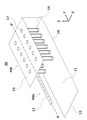
- FIG. 1 is a perspective view showing a mode conversion structure 10 according to Embodiment 1 of the present disclosure
- FIG. 2 is a side sectional view (AA' sectional view) showing the mode conversion structure 10.
- the mode conversion structure 10 includes a first dielectric substrate 11 having a microstrip line MSL and a second dielectric substrate 14 having a post wall waveguide PW.
- first thickness is different from the thickness of the second dielectric substrate 14 (second thickness).
- the thickness of the first dielectric substrate 11 may be read as the thickness of the dielectric material constituting the first dielectric substrate 11 or the thickness of the microstrip line MSL
- the thickness of the second dielectric substrate 14 may be read as the thickness of the dielectric material constituting the first dielectric substrate 11 or the thickness of the microstrip line MSL. It may also be read as the thickness of the dielectric constituting the two-dielectric substrate 14 or the thickness of the post wall waveguide PW.
- the first dielectric substrate 11 and the second dielectric substrate 14 may be composed of one substrate or may be composed of different substrates.
- the microstrip line MSL includes a first dielectric substrate 11, a line conductor 12, and GND 13 (first ground conductor). Specifically, the microstrip line MSL is configured by a line conductor 12 and GND 13 that face each other with a dielectric sandwiched therebetween on the first dielectric substrate 11 .
- the post wall waveguide PW includes a second dielectric substrate 14, a first conductor layer 15, a second conductor layer 16, and a via (via hole) 17.
- the post wall waveguide PW includes a first conductor layer 15 and a second conductor layer (waveguide wide wall or simply wide wall) that face each other with a dielectric sandwiched therebetween in the second dielectric substrate 14. 16 and opposing vias (waveguide narrow walls or simply narrow walls) 17 that electrically connect these conductor layers.
- the vias 17 are arranged in the signal transmission direction (electromagnetic wave propagation direction (transmission direction); Y direction) at intervals of less than a half wavelength ( ⁇ /2) of the electromagnetic wave.
- the line conductor 12 and the first conductor layer 15 are connected on the same plane (a plane parallel to the XY plane).
- the via (via hole) 18 (first via) electrically connects the GND 13 and the second conductor layer 16 (the GND 13 and the second conductor layer 16 electrically connected via). Therefore, unlike existing techniques, the GND 13 and the second conductor layer 16 are not connected on the same plane (a plane parallel to the XY plane).
- FIG. 3 is a perspective view showing a mode conversion structure 30 according to a comparative example
- FIG. 4 is a side sectional view (AA' sectional view) showing the mode conversion structure 30.
- the same elements as those in the mode conversion structure 10 are given the same reference numerals, and the parts different from the mode conversion structure 10 will be explained.
- the mode conversion structure 30 includes a first dielectric substrate 11 having a microstrip line MSL and a second dielectric substrate 14 having a post wall waveguide PW.
- the thickness of the first dielectric substrate 11 and the thickness of the second dielectric substrate 14 are the same, and the GND 13 and the second conductor layer 16 are arranged in the same plane (XY (plane), and there is no via corresponding to via 18. Therefore, the mode conversion structure 30 may be considered as an example of existing technology based on the mode conversion structure disclosed in Patent Document 1.
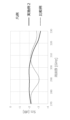
- FIG. 5 is a diagram showing the radiation power simulation results of the mode conversion structure 10 according to Example 1 and the mode conversion structure 30 according to the comparative example when a power of 0.5 W is input. From FIG. 5, it can be seen that the mode conversion structure 10 according to Example 1 radiates less power into space than the mode conversion structure 30 according to Comparative Example 1, and can reduce radiation loss. This is because the thickness of the microstrip line according to Example 1 is thinner than the thickness of the microstrip line according to the comparative example.
- the thickness of the microstrip line MSL does not need to be the same as the thickness of the post wall waveguide PW, so transmission loss can be suppressed, and the thickness of the microstrip line MSL can be suppressed.
- Line MSL and post wall waveguide PW can be connected.
- FIG. 6 is a perspective view showing a mode conversion structure 60 according to Embodiment 2 of the present disclosure
- FIG. 7 is a side sectional view (AA' sectional view) showing the mode conversion structure 60.
- the same elements as those in the mode conversion structure 10 are given the same reference numerals, and the parts different from the mode conversion structure 10 will be explained.
- the mode conversion structure 60 is arranged to extend (overlap) by about ⁇ /2.
- the GND 13 extends by about ⁇ /2 in the direction of the post wall waveguide PW (positive side of the Y-axis) with respect to the end face of the via 18 (ZX plane perpendicular to the Y-axis).
- the via 18 is arranged at a distance of about ⁇ /2 from the end surface (end) of the GND 13 in contact with the post wall waveguide PW along the electromagnetic wave propagation direction (in the negative direction of the Y axis) when viewed from the Z direction. ing.
- the GND 13 the first conductor layer 15, and the second conductor layer 16 are arranged to overlap by about ⁇ /2 in the YZ cross section.
- the end face of the GND 13 (the end face in contact with the post wall waveguide PW when viewed from the Z direction), the via 18, and the second conductor layer 16 form a short stub, which reduces the reflection of power and improves the transmission characteristics. Improve.
- FIG. 8 is a diagram showing the results of simulation of the transmission characteristics of the mode conversion structure 60 and the mode conversion structure 30.
- the horizontal axis represents the frequency (unit: GHz), and the vertical axis represents the value (unit: dB) of S21, which is an S parameter indicating the pass characteristic.
- the mode conversion structure 60 has a larger passing characteristic than the mode conversion structure 30.
- FIG. 9 is a perspective view showing a mode conversion structure 90 according to a modification of the second embodiment of the present disclosure
- FIG. 10 is a side sectional view (AA' sectional view) showing the mode conversion structure 90. .
- the post wall waveguide PW is extended by about ⁇ /2 in the direction of the microstrip line MSL (the negative direction of the Y axis) based on the ZX plane perpendicular to The positions of the GND 13 and the vias 18 in the direction are shifted by about ⁇ /2 in the negative direction of the Y axis.
- the line conductor 12, GND 13, and second conductor layer 16 are arranged to overlap by about ⁇ /2 in the YZ cross section.
- the via 18 extends from the end surface of the GND 13 in contact with the post wall waveguide PW, along the electromagnetic wave propagation direction (in the negative direction of the Y axis), when viewed from the Z direction (on the XY plane). are located some distance apart. Even with this structure, the end face of GND 13 (the end face in contact with post wall waveguide PW when viewed from the Z direction), the via 18, and the second conductor layer 16 constitute a short stub, so the reflection of power is reduced. , the passing characteristics are improved.
- the via 18 does not need to be placed directly under the position where the line conductor 12 of the microstrip line MSL and the first conductor layer 15 of the post wall waveguide PW are connected or in the vicinity thereof.
- the transmission characteristics depend on the positional relationship between the GND 13 of the microstrip line MSL, the second conductor layer 16 of the post wall waveguide PW, and the via 18.
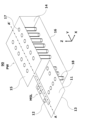
- FIG. 11 is a perspective view showing a mode conversion structure 110 according to Embodiment 3 of the present disclosure
- FIG. 12 is a side sectional view (AA' sectional view) showing the mode conversion structure 110.
- the mode conversion structure 110 the same elements as those in the mode conversion structure 60 are given the same reference numerals, and portions different from the mode conversion structure 60 will be described.
- a GND 111 (second ground conductor) is provided between the GND 13 and the second conductor layer 16.
- Mode conversion structure 110 includes GND 111 disposed between GND 13 and second conductor layer 16 .
- the GND 111 extends about 3 ⁇ /4 along the electromagnetic wave propagation direction from the end face of the via 18 (the end face in contact with the post wall waveguide PW when seen from the Z direction) when viewed from the Z direction (on the XY plane). are doing.
- the end face of GND 13 (the end face in contact with the post wall waveguide PW when viewed from the Z direction) and the end face of GND 111 (the end face in contact with the post wall waveguide PW when seen from the Z direction) are They are separated by about ⁇ /4 along the propagation direction.
- the first conductor layer 15, GND 13 and the second conductor layer 16 are arranged to overlap by about ⁇ /2 in the YZ cross section, and the first conductor layer 15, GND 111 and the second conductor layer
- the layers 16 are arranged to overlap by about 3 ⁇ /4 in the YZ cross section, and the GNDs 111 and GND 13 are arranged to overlap by about ⁇ /2 in the YZ cross section.
- a via (via hole) 112 (second via) that electrically connects the GND 111 and the second conductor layer 16 is provided.
- the mode conversion structure 110 includes a via 112 that electrically connects the GND 111 and the second conductor layer 16.
- the via 112 extends from the end face of the GND 111 (the end face in contact with the post wall waveguide PW when seen from the Z direction) along the electromagnetic wave propagation direction (in the negative direction of the Y axis) by about ⁇ /2 when viewed from the Z direction. are located far apart.
- the short stub formed by the GND 13 and the via 18 and the short stub formed by the GND 111 and the via 112 are stacked in a stepped manner.
- the phases of the reflected waves from the respective short stubs can be made to be in opposite phases.
- the present inventors conducted an electromagnetic field simulation using a finite integral method to find a mode conversion structure 110 according to Example 3 (Embodiment 3) shown in FIG. 11 and a comparative example (example based on existing technology) shown in FIG. The transmission characteristics of the mode conversion structure 30 were analyzed and compared.
- FIG. 13 is a diagram showing the results of simulation of the transmission characteristics of the mode conversion structure 110 and the mode conversion structure 30.
- the horizontal axis represents the frequency (unit: GHz), and the vertical axis represents the value of S21 (unit: dB).
- the mode conversion structure 110 has a larger passing characteristic than the mode conversion structure 30.
- FIG. 11 and FIG. 12 show an example in which the short stubs are stacked in a two-stage staircase, there is no limit to the number of stages.
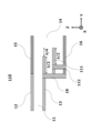
- FIG. 14 a side cross-sectional view (corresponding to the AA' cross-sectional view of other drawings) showing a mode conversion structure 140 according to a modification of the third embodiment of the present disclosure
- the GND 141 and the via 142 may be added, and the short stubs may be stacked in a three-tiered manner.
- GND and vias may be added in the same way, and the short stubs may be stacked in four or more steps.
- the mode conversion structure includes n (n is an integer of 1 or more) GNDs (GND111, GND141, etc.) disposed between GND13 and the second conductor layer 16, and each of the n GNDs and the It may also include vias (second vias; vias 112, vias 142, etc.) that electrically connect the two conductor layers 16.
- n is an integer of 1 or more GNDs (GND111, GND141, etc.) disposed between GND13 and the second conductor layer 16, and each of the n GNDs and the It may also include vias (second vias; vias 112, vias 142, etc.) that electrically connect the two conductor layers 16.
- the via 142 that electrically connects the GND 141 and the second conductor layer 16 extends from the end surface of the GND 141 (the end surface in contact with the post wall waveguide PW) along the propagation direction of electromagnetic waves when viewed from the Z direction. , may be arranged at a distance of about ⁇ /2.
- each opposing GND pair (the end faces in contact with the post wall waveguide PW) of (n+1) GNDs consisting of GND 13 and n GNDs are aligned along the propagation direction of electromagnetic waves when viewed from the Z direction. , may be separated by about ⁇ /4.
- the end faces of the opposing pair GND13 and GND111 (the end faces in contact with the post wall waveguide PW) are in the direction of electromagnetic wave propagation when viewed from the Z direction. They may be separated by about ⁇ /4 along the direction.
- the opposing pair GND111 and GND141 have their end faces (end faces in contact with the post wall waveguide PW) separated by about ⁇ /4 along the electromagnetic wave propagation direction when viewed from the Z direction. You can.
- the first conductor layer 15, GND 13, and second conductor layer 16 are arranged to overlap by about ⁇ /2 in the YZ cross section, and the first conductor layer 15, GND 111, and second conductor layer
- the layers 16 are arranged to overlap by about 3 ⁇ /4 in the YZ cross section, the first conductor layer 15, GND 141 and the second conductor layer 16 are arranged to overlap by about ⁇ in the YZ cross section, and the GND 111 and GND 13 are In the YZ cross section, the GND 111 and GND 141 are arranged to overlap by about ⁇ /2, and the GND 111 and GND 141 are arranged to overlap by about 3 ⁇ /4 in the YZ cross section.
- the mode conversion structure (mode conversion structure 10, 60, 90, 110, 140) according to the embodiment of the present disclosure has a microstrip line MSL configured by opposing line conductors 12 and GND 13, and has a first thickness.
- a second dielectric substrate 14 having a post wall waveguide PW including a first conductor layer 15 and a second conductor layer 16 facing each other, and having a second thickness that is thicker than the first thickness. and a via 18 that electrically connects the GND 13 and the second conductor layer 16.
- the line conductor 12 and the first conductor layer 15 are connected on the same plane (a plane parallel to the XY plane).
- the thickness of the microstrip line does not need to be the same as the thickness of the post wall waveguide, so transmission loss can be suppressed and it is possible to connect the microstrip line and the post wall waveguide with different thicknesses. can.
- a waveguide includes a microstrip line configured by a line conductor and a first ground conductor facing the line conductor, and a first dielectric substrate having a first thickness.
- a post wall waveguide including a first conductor layer connected on the same plane as the line conductor, and a second conductor layer facing the first conductor layer, and a second conductor layer having a thickness greater than the first thickness.
- the device includes a second dielectric substrate having a thickness, and a first via that electrically connects the first ground conductor and the second conductor layer.
- the thickness of the microstrip line does not need to be the same as the thickness of the post wall waveguide, so transmission loss can be suppressed, and it is possible to connect the microstrip line and the post wall waveguide with different thicknesses. I can do it.
- the first via is configured to transmit electromagnetic waves propagating through the post wall waveguide from an end of the first ground conductor in contact with the post wall waveguide when viewed from a direction perpendicular to the same plane.
- the electromagnetic waves are spaced apart from each other by approximately half a wavelength of the electromagnetic waves along the propagation direction.
- the end of the first ground conductor, the first via, and the second conductor layer form a short stub, which reduces reflection of power and improves transmission characteristics.
- This mode conversion structure includes a second ground conductor disposed between the first ground conductor and the second conductor layer, and a second ground conductor that electrically connects the second ground conductor and the second conductor layer.
- the second via extends from the end of the second ground conductor in contact with the post wall waveguide along the propagation direction when viewed from a direction perpendicular to the same plane.
- the end portion of the first ground conductor that is in contact with the post wall waveguide and the end portion of the second ground conductor that is in contact with the post wall waveguide are disposed approximately half a wavelength of electromagnetic waves apart, and that the end portion of the first ground conductor that is in contact with the post wall waveguide is on the same plane. When viewed in the vertical direction, they are separated by approximately a quarter wavelength of the electromagnetic waves.
- the short stubs are stacked and the reflected waves from the short stubs are canceled, so it is possible to reduce loss due to reflection and further improve the transmission characteristics.
- This mode conversion structure includes n ground conductors (n is an integer of 1 or more) disposed between the first ground conductor and the second conductor layer, and each of the n ground conductors and the a second via electrically connecting the second conductor layer, the second via being connected to the n ground conductors in contact with the post wall waveguide when viewed from a direction perpendicular to the same plane. along the propagation direction from each end of the electromagnetic wave by approximately half a wavelength of the electromagnetic wave.
- an end in contact with the post wall waveguide among the ends of each opposing ground conductor pair of (n+1) ground conductors including the first ground conductor and the n ground conductors. are separated by approximately a quarter wavelength of the electromagnetic waves when viewed from a direction perpendicular to the same plane.
- the reflected waves from the short stub are canceled, so it is possible to reduce loss due to reflection and further improve the transmission characteristics.
- the first ground conductor, the first conductor layer, and the second conductor layer are arranged along the propagation direction of the electromagnetic wave propagating in the post wall waveguide.
- the electromagnetic waves are arranged so as to overlap approximately half the wavelength of the electromagnetic waves.
- the first ground conductor, the line conductor, and the second conductor layer are arranged along the propagation direction of the electromagnetic wave propagating in the post wall waveguide. They are arranged to overlap approximately half the wavelength of the electromagnetic waves.
- An embodiment of the present disclosure is useful for a mode conversion structure for connecting a microstrip line and a post wall waveguide.
- Mode conversion structure 11 First dielectric substrate 12 Line conductor 13 Ground conductor 14 Second dielectric substrate 15 First conductor layer 16 Second conductor layer 17 Via (via hole) 18 Via (Beer Hall) 30 Mode conversion structure 60 Mode conversion structure 90 Mode conversion structure 110 Mode conversion structure 111 Ground conductor 112 Via (via hole) 140 Mode conversion structure 141 Ground conductor 142 Via (via hole)
Landscapes
- Waveguides (AREA)
Abstract
本開示の一実施例に係るモード変換構造は、線路導体、及び、前記線路導体に対向する第1グランド導体によって構成されているマイクロストリップ線路を有し、第1厚みを有する第1誘電体基板と、前記線路導体と同一平面上で接続されている第1導体層、及び、前記第1導体層に対向する第2導体層を含むポスト壁導波路を有し、前記第1厚みより厚い第2厚みを有する第2誘電体基板と、前記第1グランド導体と前記第2導体層とを電気的に接続する第1ビアと、を備える。
Description
本開示は、モード変換構造に関する。
誘電体基板上で高周波信号を伝送する手段として、マイクロストリップ線路が利用されることが多い。しかしながら、ミリ波、テラヘルツ波等の周波数帯においては、高周波固有の現象である表皮効果及び界面凹凸の影響により、導体損による伝送損失が大きくなる。
マイクロストリップ線路を構成する誘電体(基板)を厚くすることにより、導体損失を小さくできるが、この場合、電磁波としてエネルギーを放射する放射損失が大きくなってしまい、伝送損失を小さくすることが困難である。
一方で、伝送損失を小さくする手段の1つとして、誘電体を1対の導体層で挟み、信号の伝送方向(電磁波の伝搬方向)にλ/2(λ:電磁波の波長)の間隔で配列されたビアホール群で導体層同士を電気的に接続し、主導体層を導波管の広壁として用い、ビアホール群を導波管の狭壁として用いるポスト壁導波路構造がある。ポスト壁導波路は、四方を導体で囲まれているため、基板厚を厚くしても、放射損失が増加しない。そのため、誘電体を厚くすることができ、導体損失と放射損失とを同時に小さくすることが可能である。
高周波信号を発生させる集積回路(IC:Integrated Circuit)の実装を考えると、ICは、半田ボールを介してマイクロストリップ線路に実装されることが多く、ポスト壁導波路に直接給電することは困難である。そのため、ポスト壁導波路を伝送路として用いる場合、マイクロストリップ線路とポスト壁導波路とを接続する伝搬(伝送)モード変換構造(以下、単にモード変換構造と呼ぶ)が構成される。なお、モード変換構造は、モード変換装置等で読み替えられてもよい。
モード変換構造の既存の技術として、例えば特許文献1には、マイクロストリップ線路の線路導体とポスト壁導波路の一方の広壁とが同一平面にあり、かつ、マイクロストリップ線路のグランド導体(以下、GND)とポスト壁導波路のもう一方の広壁とが同一平面にある(同一厚みのマイクロストリップ線路とポスト壁導波路とを接続する)モード変換構造が開示されている。
しかしながら、特許文献1に記載の既存の技術では、マイクロストリップ線路の厚みとポスト壁導波路の厚みとが同一であるため、厚みが異なるマイクロストリップ線路とポスト壁導波路とを接続することが困難である。
特許文献1に記載の既存の技術では、薄いマイクロストリップ線路と薄いポスト壁導波路とを接続する場合、放射損が小さく、導体損が大きくなり、厚いマイクロストリップ線路と厚いポスト壁導波路とを接続する場合、導体損が小さく、放射損が大きくなってしまい、マイクロストリップ線路の放射損失又はポスト壁導波路の導体損失を小さくすることが困難である。
本開示の非限定的な実施例は、伝送損失を抑制しつつ、厚みが異なるマイクロストリップ線路とポスト壁導波路とを接続することができるモード変換構造の提供に資する。
本開示の一実施例に係るモード変換構造は、線路導体、及び、前記線路導体に対向する第1グランド導体によって構成されているマイクロストリップ線路を有し、第1厚みを有する第1誘電体基板と、前記線路導体と同一平面上で接続されている第1導体層、及び、前記第1導体層に対向する第2導体層を含むポスト壁導波路を有し、前記第1厚みより厚い第2厚みを有する第2誘電体基板と、前記第1グランド導体と前記第2導体層とを電気的に接続する第1ビアと、を備える。
本開示の一実施例によれば、伝送損失を抑制しつつ、厚みが異なるマイクロストリップ線路とポスト壁導波路とを接続することができる。
本開示の一実施例における更なる利点及び効果は、明細書及び図面から明らかにされる。かかる利点及び/又は効果は、いくつかの実施形態並びに明細書及び図面に記載された特徴によってそれぞれ提供されるが、1つ又はそれ以上の同一の特徴を得るために必ずしも全てが提供される必要はない。
以下、図面を適宜参照して、本開示の実施の形態について、詳細に説明する。但し、必要以上に詳細な説明は省略する場合がある。例えば、既によく知られた事項の詳細説明や実質的に同一の構成に対する重複説明を省略する場合がある。これは、以下の説明が不必要に冗長になるのを避け、当業者の理解を容易にするためである。
なお、添付図面及び以下の説明は、当業者が本開示を十分に理解するために、提供されるのであって、これらにより特許請求の範囲に記載の主題を限定することは意図されていない。
本明細書において、図面に示すZ軸正方向を上(方向)と呼び、Z軸負方向を下(方向)と呼ぶ。また、各種図面において、見やすくするために、モード変換構造の側面(図面に示すYZ面に平行な面)等のいくつかの要素は、省略されており、また、いくつかの要素は、縮尺通りに描かれていないことがある。
(実施の形態1)
<モード変換構造の構成>
図1は、本開示の実施の形態1に係るモード変換構造10を示す斜視図であり、図2は、モード変換構造10を示す側面断面図(A-A’断面図)である。
<モード変換構造の構成>
図1は、本開示の実施の形態1に係るモード変換構造10を示す斜視図であり、図2は、モード変換構造10を示す側面断面図(A-A’断面図)である。
図1及び図2に示すように、モード変換構造10は、マイクロストリップ線路MSLを有する第1誘電体基板11と、ポスト壁導波路PWを有する第2誘電体基板14と、を備える。ここで、第1誘電体基板11の厚み(第1厚み)と第2誘電体基板14の厚み(第2厚み)とは異なる(第2誘電体基板14の厚みは、第1誘電体基板11の厚みより厚い)。
なお、第1誘電体基板11の厚みは、第1誘電体基板11を構成する誘電体の厚み又はマイクロストリップ線路MSLの厚みで読み替えられてもよく、第2誘電体基板14の厚みは、第2誘電体基板14を構成する誘電体の厚み又はポスト壁導波路PWの厚みで読み替えられてもよい。なお、第1誘電体基板11と第2誘電体基板14とは、1つの基板で構成されてもよいし、異なる基板で構成されてもよい。
図1に示すように、マイクロストリップ線路MSLは、第1誘電体基板11と、線路導体12と、GND13(第1グランド導体)と、を含む。具体的には、マイクロストリップ線路MSLは、第1誘電体基板11において誘電体を挟む対向する線路導体12及びGND13によって構成されている。
図1に示すように、ポスト壁導波路PWは、第2誘電体基板14と、第1導体層15と、第2導体層16と、ビア(ビアホール)17と、を含む。具体的には、ポスト壁導波路PWは、第2誘電体基板14において誘電体を挟む対向する第1導体層15及び第2導体層(導波路広壁又は単に広壁(を構成する))16とこれらの導体層を電気的に接続する対向するビア(導波路狭壁又は単に狭壁(を構成する))17とによって構成されている。なお、ビア17は、信号の伝送方向(電磁波の伝搬方向(伝送方向);Y方向)に、電磁波の半波長(λ/2)以下の間隔で配列されている。
図2に示すように、線路導体12と第1導体層15とは、同一平面(XY平面に平行な平面)上で接続されている。
図1及び図2に示すように、ビア(ビアホール)18(第1ビア)は、GND13と第2導体層16とを電気的に接続する(GND13と第2導体層16とは、ビア18を介して電気的に接続される)。したがって、既存の技術と異なり、GND13と第2導体層16とは、同一平面(XY平面に平行な平面)上で接続されていない。
<比較例>
図3は、比較例に係るモード変換構造30を示す斜視図であり、図4は、モード変換構造30を示す側面断面図(A-A’断面図)である。なお、モード変換構造30において、モード変換構造10と同一の要素については同一の符号を付し、モード変換構造10と異なる部分について説明する。
図3は、比較例に係るモード変換構造30を示す斜視図であり、図4は、モード変換構造30を示す側面断面図(A-A’断面図)である。なお、モード変換構造30において、モード変換構造10と同一の要素については同一の符号を付し、モード変換構造10と異なる部分について説明する。
図3及び図4に示すように、モード変換構造30は、マイクロストリップ線路MSLを有する第1誘電体基板11と、ポスト壁導波路PWを有する第2誘電体基板14と、を備える。モード変換構造10と異なり、モード変換構造30では、第1誘電体基板11の厚みと第2誘電体基板14の厚みとは同一であり、GND13と第2導体層16とが、同一平面(XY平面)上に存在し、ビア18に対応するビアが存在しない。したがって、モード変換構造30は、特許文献1に開示されているモード変換構造に基づく既存の技術による例と捉えられてよい。
<比較>
本発明者らは、有限積分法を用いた電磁界シミュレーションによって、図1に示す実施例1(実施の形態1)に係るモード変換構造10を用いて、厚み0.1mmのマイクロストリップ線路と厚み0.2mmのポスト壁導波路とを接続した場合、及び、図3に示す比較例(既存の技術による例)に係るモード変換構造30を用いて、厚み0.2mmのマイクロストリップ線路と厚み0.2mmのポスト壁導波路とを接続した場合の300GHzにおける放射電力を解析し、放射損失の比較を行った。
本発明者らは、有限積分法を用いた電磁界シミュレーションによって、図1に示す実施例1(実施の形態1)に係るモード変換構造10を用いて、厚み0.1mmのマイクロストリップ線路と厚み0.2mmのポスト壁導波路とを接続した場合、及び、図3に示す比較例(既存の技術による例)に係るモード変換構造30を用いて、厚み0.2mmのマイクロストリップ線路と厚み0.2mmのポスト壁導波路とを接続した場合の300GHzにおける放射電力を解析し、放射損失の比較を行った。
図5は、0.5Wの電力を入力した場合における、実施例1に係るモード変換構造10及び比較例に係るモード変換構造30の放射電力シミュレーション結果を示す図である。図5から、実施例1に係るモード変換構造10の方が、比較例1に係るモード変換構造30よりも空間に放射する電力が小さくなり、放射損失を小さくできることがわかる。これは、実施例1に係るマイクロストリップ線路の厚みが、比較例に係るマイクロストリップ線路の厚みよりも薄いためである。
このように、モード変換構造10は、マイクロストリップ線路MSLの厚みをポスト壁導波路PWの厚みと同一にしないでよいので、伝送損失を抑制することができ、誘電体基板の厚みが異なるマイクロストリップ線路MSLとポスト壁導波路PWとを接続することができる。
(実施の形態2)
<モード変換構造の構成>
図6は、本開示の実施の形態2に係るモード変換構造60を示す斜視図であり、図7は、モード変換構造60を示す側面断面図(A-A’断面図)である。なお、モード変換構造60において、モード変換構造10と同一の要素については同一の符号を付し、モード変換構造10と異なる部分について説明する。
<モード変換構造の構成>
図6は、本開示の実施の形態2に係るモード変換構造60を示す斜視図であり、図7は、モード変換構造60を示す側面断面図(A-A’断面図)である。なお、モード変換構造60において、モード変換構造10と同一の要素については同一の符号を付し、モード変換構造10と異なる部分について説明する。
モード変換構造10と異なり、図7に示すように、モード変換構造60では、線路導体12と並行して配置されたGND13が、更に、第1導体層15と第2導体層16との間に、λ/2程度延伸(重複)して配置されている。GND13は、ビア18の端面(Y軸に垂直なZX平面)を基準にしてポスト壁導波路PWの方向(Y軸正側)へλ/2程度延伸されている。ビア18は、Z方向から見て、ポスト壁導波路PWに接するGND13の端面(端部)から、電磁波の伝搬方向に沿って、(Y軸の負方向に)λ/2程度離れて配置されている。図7に示すモード変換構造60では、GND13、第1導体層15及び第2導体層16が、YZ断面において、λ/2程度重複して配置されている。
これにより、GND13の端面(Z方向から見てポスト壁導波路PWに接する端面)とビア18と第2導体層16とが、ショートスタブを構成するので、電力の反射が小さくなり、通過特性が改善する。
<比較>
本発明者らは、有限積分法を用いた電磁界シミュレーションによって、図6に示す実施例2(実施の形態2)に係るモード変換構造60及び図3に示す比較例(既存の技術による例)に係るモード変換構造30の通過特性を解析及び比較した。
本発明者らは、有限積分法を用いた電磁界シミュレーションによって、図6に示す実施例2(実施の形態2)に係るモード変換構造60及び図3に示す比較例(既存の技術による例)に係るモード変換構造30の通過特性を解析及び比較した。
図8は、モード変換構造60及びモード変換構造30の通過特性シミュレーション結果を示す図である。図8において、横軸は周波数(単位:GHz)を表し、縦軸は通過特性を示すSパラメータであるS21の値(単位:dB)を表す。
図8から、周波数が300GHzである場合において、モード変換構造60の方が、モード変換構造30よりも通過特性が大きいことがわかる。
<変形例>
図9は、本開示の実施の形態2の変形例に係るモード変換構造90を示す斜視図であり、図10は、モード変換構造90を示す側面断面図(A-A’断面図)である。
図9は、本開示の実施の形態2の変形例に係るモード変換構造90を示す斜視図であり、図10は、モード変換構造90を示す側面断面図(A-A’断面図)である。
本変形例では、図10に示すように、Z方向から見て(XY平面において)主導体層(第2導体層)16を、線路導体12と第1導体層15との接続面(Y軸に垂直なZX平面)を基準にして、ポスト壁導波路PWからマイクロストリップ線路MSLの方向(Y軸の負方向)にλ/2程度延伸し、モード変換構造60の構成から、Y軸の負方向のGND13及びビア18の位置をY軸の負方向へλ/2程度ずらしている。図10に示すモード変換構造90では、線路導体12、GND13及び第2導体層16が、YZ断面において、λ/2程度重複して配置されている。この場合も、ビア18は、Z方向から見て(XY平面において)、ポスト壁導波路PWに接するGND13の端面から、電磁波の伝搬方向に沿って、(Y軸の負方向に)λ/2程度離れて配置されている。この構造であっても、GND13の端面(Z方向から見てポスト壁導波路PWに接する端面)とビア18と第2導体層16とが、ショートスタブを構成するので、電力の反射が小さくなり、通過特性が改善する。
このように、ビア18は、マイクロストリップ線路MSLの線路導体12とポスト壁導波路PWの第1導体層15とが接続される位置又はその近傍の直下に配置されなくてもよい。通過特性は、マイクロストリップ線路MSLのGND13とポスト壁導波路PWの第2導体層16とビア18との位置関係に依存する。
(実施の形態3)
<モード変換構造の構成>
図11は、本開示の実施の形態3に係るモード変換構造110を示す斜視図であり、図12は、モード変換構造110を示す側面断面図(A-A’断面図)である。なお、モード変換構造110において、モード変換構造60と同一の要素については同一の符号を付し、モード変換構造60と異なる部分について説明する。
<モード変換構造の構成>
図11は、本開示の実施の形態3に係るモード変換構造110を示す斜視図であり、図12は、モード変換構造110を示す側面断面図(A-A’断面図)である。なお、モード変換構造110において、モード変換構造60と同一の要素については同一の符号を付し、モード変換構造60と異なる部分について説明する。
モード変換構造60と異なり、図11及び図12に示すように、モード変換構造110では、GND13と第2導体層16との間にGND111(第2グランド導体)が設けられている。モード変換構造110は、GND13と第2導体層16との間に配置されているGND111を備える。また、GND111は、Z方向から見て(XY平面において)、ビア18の端面(Z方向から見てポスト壁導波路PWに接する端面)から、電磁波の伝搬方向に沿って、3λ/4程度延伸している。したがって、GND13の端面(Z方向から見てポスト壁導波路PWに接する端面)とGND111の端面(Z方向から見てポスト壁導波路PWに接する端面)とは、Z方向から見て、電磁波の伝搬方向に沿って、λ/4程度離れている。図12に示すモード変換構造110では、第1導体層15、GND13及び第2導体層16が、YZ断面において、λ/2程度重複して配置され、第1導体層15、GND111及び第2導体層16が、YZ断面において、3λ/4程度重複して配置され、GND111及びGND13がYZ断面において、λ/2程度重複して配置されている。
加えて、モード変換構造60と異なり、図11及び図12に示すように、GND111と第2導体層16とを電気的に接続するビア(ビアホール)112(第2ビア)が設けられている。モード変換構造110は、GND111と第2導体層16とを電気的に接続するビア112を備える。ビア112は、Z方向から見て、GND111の端面(Z方向から見てポスト壁導波路PWに接する端面)から、電磁波の伝搬方向に沿って、(Y軸の負方向に)λ/2程度離れて配置されている。
結果として、GND13とビア18とによって構成されるショートスタブと、GND111とビア112とによって構成されるショートスタブと、が、階段状に積層されている。
このように、それぞれのショートスタブをλ/4程度ずらして配置することで、それぞれのショートスタブからの反射波の位相を逆位相にすることができる。これにより、反射波を打ち消し合うため、反射による損失を軽減することができ、モード変換構造110(接続部)の通過特性をさらに改善することができる。
<比較>
本発明者らは、有限積分法を用いた電磁界シミュレーションによって、図11に示す実施例3(実施の形態3)に係るモード変換構造110及び図3に示す比較例(既存の技術による例)に係るモード変換構造30の通過特性を解析及び比較した。
本発明者らは、有限積分法を用いた電磁界シミュレーションによって、図11に示す実施例3(実施の形態3)に係るモード変換構造110及び図3に示す比較例(既存の技術による例)に係るモード変換構造30の通過特性を解析及び比較した。
図13は、モード変換構造110及びモード変換構造30の通過特性シミュレーション結果を示す図である。図13において、横軸は周波数(単位:GHz)を表し、縦軸はS21の値(単位:dB)を表す。
図13から、周波数が300GHzである場合において、モード変換構造110の方が、モード変換構造30よりも通過特性が大きいことがわかる。
<変形例>
図11及び図12では、ショートスタブが、2段の階段状に積層されている例を示したが、段数に制限はない。例えば、図14(本開示の実施の形態3の変形例に係るモード変換構造140を示す側面断面図(他の図面のA-A’断面図に相当))に示すように、GND141及びビア142を追加し、ショートスタブが、3段の階段状に積層されてもよい。もちろん、同様に、GND及びビアを追加し、ショートスタブが、4段以上の階段状に積層されてもよい。
図11及び図12では、ショートスタブが、2段の階段状に積層されている例を示したが、段数に制限はない。例えば、図14(本開示の実施の形態3の変形例に係るモード変換構造140を示す側面断面図(他の図面のA-A’断面図に相当))に示すように、GND141及びビア142を追加し、ショートスタブが、3段の階段状に積層されてもよい。もちろん、同様に、GND及びビアを追加し、ショートスタブが、4段以上の階段状に積層されてもよい。
例えば、モード変換構造は、GND13と第2導体層16との間に配置されているn個(nは1以上の整数)のGND(GND111、GND141等)と、n個のGNDの各々と第2導体層16とを電気的に接続するビア(第2ビア;ビア112、ビア142等)と、を備えてもよい。
また、n個のGNDの各々と第2導体層16とを電気的に接続するビアは、Z方向から見て(XY平面において)、n個のGNDの各々の端面(ポスト壁導波路PWに接する端面)から、電磁波の伝搬方向に沿って、λ/2程度離れて配置されていてもよい。例えば、図14に示すようにn=2である場合、GND111と第2導体層16とを電気的に接続するビア112は、Z方向から見て、GND111の端面(ポスト壁導波路PWに接する端面)から、電磁波の伝搬方向に沿って、λ/2程度離れて配置されていてもよい。また、例えば、GND141と第2導体層16とを電気的に接続するビア142は、Z方向から見て、GND141の端面(ポスト壁導波路PWに接する端面)から、電磁波の伝搬方向に沿って、λ/2程度離れて配置されていてもよい。
また、GND13とn個のGNDとからなる(n+1)個のGNDの各対向するGNDペアの端面(ポスト壁導波路PWに接する端面)は、Z方向から見て、電磁波の伝搬方向に沿って、λ/4程度離れていてもよい。例えば、図14に示すようにn=2である場合、対向するペアであるGND13とGND111とは、それらの端面(ポスト壁導波路PWに接する端面)が、Z方向から見て、電磁波の伝搬方向に沿って、λ/4程度離れていてもよい。また、例えば、対向するペアであるGND111とGND141とは、それらの端面(ポスト壁導波路PWに接する端面)が、Z方向から見て、電磁波の伝搬方向に沿って、λ/4程度離れていてもよい。図14に示すモード変換構造140では、第1導体層15、GND13及び第2導体層16が、YZ断面において、λ/2程度重複して配置され、第1導体層15、GND111及び第2導体層16が、YZ断面において、3λ/4程度重複して配置され、第1導体層15、GND141及び第2導体層16が、YZ断面において、λ程度重複して配置され、GND111及びGND13が、YZ断面において、λ/2程度重複して配置され、GND111及びGND141が、YZ断面において、3λ/4程度重複して配置されている。
<実施の形態の効果>
本開示の実施の形態に係るモード変換構造(モード変換構造10、60、90、110、140)は、対向する線路導体12及びGND13によって構成されているマイクロストリップ線路MSLを有し、第1厚みを有する第1誘電体基板11と、対向する第1導体層15及び第2導体層16を含むポスト壁導波路PWを有し、第1厚みより厚い第2厚みを有する第2誘電体基板14と、GND13と第2導体層16とを電気的に接続するビア18と、を備える。線路導体12と第1導体層15とは、同一平面(XY平面に平行な平面)上で接続されている。
本開示の実施の形態に係るモード変換構造(モード変換構造10、60、90、110、140)は、対向する線路導体12及びGND13によって構成されているマイクロストリップ線路MSLを有し、第1厚みを有する第1誘電体基板11と、対向する第1導体層15及び第2導体層16を含むポスト壁導波路PWを有し、第1厚みより厚い第2厚みを有する第2誘電体基板14と、GND13と第2導体層16とを電気的に接続するビア18と、を備える。線路導体12と第1導体層15とは、同一平面(XY平面に平行な平面)上で接続されている。
この構成により、マイクロストリップ線路の厚みをポスト壁導波路の厚みと同一にしないでよいので、伝送損失を抑制することができ、厚みが異なるマイクロストリップ線路とポスト壁導波路とを接続することができる。
<実施の形態のまとめ>
本開示の一実施例に係る導波路は、線路導体、及び、前記線路導体に対向する第1グランド導体によって構成されているマイクロストリップ線路を有し、第1厚みを有する第1誘電体基板と、前記線路導体と同一平面上で接続されている第1導体層、及び、前記第1導体層に対向する第2導体層を含むポスト壁導波路を有し、前記第1厚みより厚い第2厚みを有する第2誘電体基板と、前記第1グランド導体と前記第2導体層とを電気的に接続する第1ビアと、を備える。
本開示の一実施例に係る導波路は、線路導体、及び、前記線路導体に対向する第1グランド導体によって構成されているマイクロストリップ線路を有し、第1厚みを有する第1誘電体基板と、前記線路導体と同一平面上で接続されている第1導体層、及び、前記第1導体層に対向する第2導体層を含むポスト壁導波路を有し、前記第1厚みより厚い第2厚みを有する第2誘電体基板と、前記第1グランド導体と前記第2導体層とを電気的に接続する第1ビアと、を備える。
上記の構成により、マイクロストリップ線路の厚みをポスト壁導波路の厚みと同一にしないでよいので、伝送損失を抑制することができ、厚みが異なるマイクロストリップ線路とポスト壁導波路とを接続することができる。
本モード変換構造において、前記第1ビアは、前記同一平面に垂直な方向から見て、前記ポスト壁導波路に接する前記第1グランド導体の端部から、前記ポスト壁導波路を伝搬する電磁波の伝搬方向に沿って、前記電磁波の略半波長離れて配置されている。
上記の構成により、第1グランド導体の端部と第1ビアと第2導体層とが、ショートスタブを構成するので、電力の反射が小さくなり、通過特性を改善することができる。
本モード変換構造は、前記第1グランド導体と前記第2導体層との間に配置されている第2グランド導体と、前記第2グランド導体と前記第2導体層とを電気的に接続する第2ビアと、をさらに備え、前記第2ビアは、前記同一平面に垂直な方向から見て、前記ポスト壁導波路に接する前記第2グランド導体の端部から、前記伝搬方向に沿って、前記電磁波の略半波長離れて配置されており、前記ポスト壁導波路に接する前記第1グランド導体の端部と前記ポスト壁導波路に接する前記第2グランド導体の端部とは、前記同一平面に垂直な方向から見て、前記電磁波の略四分の一波長離れている。
上記の構成により、ショートスタブが積層され、ショートスタブからの反射波が打ち消されるため、反射による損失を軽減することができ、通過特性をさらに改善することができる。
本モード変換構造は、前記第1グランド導体と前記第2導体層との間に配置されているn個(nは1以上の整数)のグランド導体と、前記n個のグランド導体の各々と前記第2導体層とを電気的に接続する第2ビアと、をさらに備え、前記第2ビアは、前記同一平面に垂直な方向から見て、前記ポスト壁導波路に接する前記n個のグランド導体の各々の端部から、前記伝搬方向に沿って、前記電磁波の略半波長離れて配置されている。
上記の構成により、ショートスタブが構成されるので、電力の反射が小さくなり、通過特性を改善することができる。
本モード変換構造において、前記第1グランド導体と前記n個のグランド導体とを含む(n+1)個のグランド導体の各対向するグランド導体ペアの端部のうち、前記ポスト壁導波路に接する端部の各々は、前記同一平面に垂直な方向から見て、前記電磁波の略四分の一波長離れている。
上記の構成により、ショートスタブからの反射波が打ち消されるため、反射による損失を軽減することができ、通過特性をさらに改善することができる。
本モード変換構造において、前記同一平面に垂直な方向から見て、前記第1グランド導体、前記第1導体層及び前記第2導体層は、前記ポスト壁導波路を伝搬する電磁波の伝搬方向に沿って、前記電磁波の略半波長重複して配置されている。
本モード変換構造において、前記同一平面に垂直な方向から見て、前記第1グランド導体、前記線路導体及び前記第2導体層は、前記ポスト壁導波路を伝搬する電磁波の伝搬方向に沿って、前記電磁波の略半波長重複して配置されている。
以上、図面を参照しながら実施の形態について説明したが、本開示はかかる例に限定されない。当業者であれば、特許請求の範囲に記載された範疇において、各種の変更例または修正例に想到し得ることは明らかである。そのような変更例または修正例についても、本開示の技術的範囲に属するものと了解される。また、本開示の趣旨を逸脱しない範囲において、実施の形態における各構成要素は任意に組み合わされてよい。
2022年5月26日出願の特願2022-085966の日本出願に含まれる明細書、図面および要約書の開示内容は、すべて本願に援用される。
本開示の一実施例は、マイクロストリップ線路とポスト壁導波路とを接続するためのモード変換構造に有用である。
10 モード変換構造
11 第1誘電体基板
12 線路導体
13 グランド導体
14 第2誘電体基板
15 第1導体層
16 第2導体層
17 ビア(ビアホール)
18 ビア(ビアホール)
30 モード変換構造
60 モード変換構造
90 モード変換構造
110 モード変換構造
111 グランド導体
112 ビア(ビアホール)
140 モード変換構造
141 グランド導体
142 ビア(ビアホール)
11 第1誘電体基板
12 線路導体
13 グランド導体
14 第2誘電体基板
15 第1導体層
16 第2導体層
17 ビア(ビアホール)
18 ビア(ビアホール)
30 モード変換構造
60 モード変換構造
90 モード変換構造
110 モード変換構造
111 グランド導体
112 ビア(ビアホール)
140 モード変換構造
141 グランド導体
142 ビア(ビアホール)
Claims (7)
- 線路導体、及び、前記線路導体に対向する第1グランド導体によって構成されているマイクロストリップ線路を有し、第1厚みを有する第1誘電体基板と、
前記線路導体と同一平面上で接続されている第1導体層、及び、前記第1導体層に対向する第2導体層を含むポスト壁導波路を有し、前記第1厚みより厚い第2厚みを有する第2誘電体基板と、
前記第1グランド導体と前記第2導体層とを電気的に接続する第1ビアと、
を備えるモード変換構造。 - 前記第1ビアは、前記同一平面に垂直な方向から見て、前記ポスト壁導波路に接する前記第1グランド導体の端部から、前記ポスト壁導波路を伝搬する電磁波の伝搬方向に沿って、前記電磁波の略半波長離れて配置されている、
請求項1に記載のモード変換構造。 - 前記第1グランド導体と前記第2導体層との間に配置されている第2グランド導体と、
前記第2グランド導体と前記第2導体層とを電気的に接続する第2ビアと、
をさらに備え、
前記第2ビアは、前記同一平面に垂直な方向から見て、前記ポスト壁導波路に接する前記第2グランド導体の端部から、前記伝搬方向に沿って、前記電磁波の略半波長離れて配置されており、
前記ポスト壁導波路に接する前記第1グランド導体の端部と前記ポスト壁導波路に接する前記第2グランド導体の端部とは、前記同一平面に垂直な方向から見て、前記電磁波の略四分の一波長離れている、
請求項2に記載のモード変換構造。 - 前記第1グランド導体と前記第2導体層との間に配置されているn個(nは1以上の整数)のグランド導体と、
前記n個のグランド導体の各々と前記第2導体層とを電気的に接続する第2ビアと、
をさらに備え、
前記第2ビアは、前記同一平面に垂直な方向から見て、前記ポスト壁導波路に接する前記n個のグランド導体の各々の端部から、前記伝搬方向に沿って、前記電磁波の略半波長離れて配置されている、
請求項2に記載のモード変換構造。 - 前記第1グランド導体と前記n個のグランド導体とを含む(n+1)個のグランド導体の各対向するグランド導体ペアの端部のうち、前記ポスト壁導波路に接する端部の各々は、前記同一平面に垂直な方向から見て、前記電磁波の略四分の一波長離れている、
請求項4に記載のモード変換構造。 - 前記同一平面に垂直な方向から見て、前記第1グランド導体、前記第1導体層及び前記第2導体層は、前記ポスト壁導波路を伝搬する電磁波の伝搬方向に沿って、前記電磁波の略半波長重複して配置されている、
請求項1に記載のモード変換構造。 - 前記同一平面に垂直な方向から見て、前記第1グランド導体、前記線路導体及び前記第2導体層は、前記ポスト壁導波路を伝搬する電磁波の伝搬方向に沿って、前記電磁波の略半波長重複して配置されている、
請求項1に記載のモード変換構造。
Applications Claiming Priority (2)
| Application Number | Priority Date | Filing Date | Title |
|---|---|---|---|
| JP2022-085966 | 2022-05-26 | ||
| JP2022085966 | 2022-05-26 |
Publications (1)
| Publication Number | Publication Date |
|---|---|
| WO2023228456A1 true WO2023228456A1 (ja) | 2023-11-30 |
Family
ID=88918901
Family Applications (1)
| Application Number | Title | Priority Date | Filing Date |
|---|---|---|---|
| PCT/JP2022/047315 WO2023228456A1 (ja) | 2022-05-26 | 2022-12-22 | モード変換構造 |
Country Status (1)
| Country | Link |
|---|---|
| WO (1) | WO2023228456A1 (ja) |
Citations (2)
| Publication number | Priority date | Publication date | Assignee | Title |
|---|---|---|---|---|
| JP2011139244A (ja) * | 2009-12-28 | 2011-07-14 | Kyocera Corp | 高周波モジュール |
| JP2016111459A (ja) * | 2014-12-04 | 2016-06-20 | アンリツ株式会社 | ミリ波帯伝送路変換構造 |
-
2022
- 2022-12-22 WO PCT/JP2022/047315 patent/WO2023228456A1/ja unknown
Patent Citations (2)
| Publication number | Priority date | Publication date | Assignee | Title |
|---|---|---|---|---|
| JP2011139244A (ja) * | 2009-12-28 | 2011-07-14 | Kyocera Corp | 高周波モジュール |
| JP2016111459A (ja) * | 2014-12-04 | 2016-06-20 | アンリツ株式会社 | ミリ波帯伝送路変換構造 |
Similar Documents
| Publication | Publication Date | Title |
|---|---|---|
| US6674347B1 (en) | Multi-layer substrate suppressing an unwanted transmission mode | |
| JP4568235B2 (ja) | 伝送路変換器 | |
| JP4184747B2 (ja) | 基板上の伝送線路と導波管との間の電気信号の変換を行う構造体 | |
| JP2004153367A (ja) | 高周波モジュール、ならびにモード変換構造および方法 | |
| US9456499B2 (en) | Structural body and interconnect substrate | |
| US8952266B2 (en) | Structural body and interconnect substrate | |
| JP2006024618A (ja) | 配線基板 | |
| US9214715B2 (en) | Hybrid coupler device having plural transmission line structures with unwound-rewound geometry | |
| EP0735604B1 (en) | Planar dielectric line and integrated circuit using the same | |
| US10811753B2 (en) | Hollow-waveguide-to-planar-waveguide transition including a coupling conductor having one or more conductors branching therefrom | |
| WO2023228456A1 (ja) | モード変換構造 | |
| JP3119191B2 (ja) | 平面誘電体集積回路 | |
| US11228077B2 (en) | Microstrip DC block | |
| US10840609B1 (en) | Low-profile rectangular to circular transition | |
| JPH04122106A (ja) | マイクロストリップアンテナ | |
| JPH07120888B2 (ja) | 複数面導波管結合器 | |
| JP4680076B2 (ja) | 高周波回路チップの実装構造 | |
| WO2023042466A1 (ja) | 導波路 | |
| WO2023119706A1 (ja) | 伝送線路 | |
| JP7077137B2 (ja) | 伝送線路およびコネクタ | |
| WO2024023903A1 (ja) | マイクロストリップ線路-導波管変換器 | |
| JP2000174515A (ja) | コプレーナウェーブガイド−導波管変換装置 | |
| WO2024009339A1 (ja) | マイクロストリップ線路-導波管変換器 | |
| JP3895716B2 (ja) | 高周波伝送基板および高周波伝送基板接続構造 | |
| WO2004082080A1 (ja) | 同軸コネクタと多層基板との接続構造 |
Legal Events
| Date | Code | Title | Description |
|---|---|---|---|
| 121 | Ep: the epo has been informed by wipo that ep was designated in this application |
Ref document number: 22943855 Country of ref document: EP Kind code of ref document: A1 |