WO2023228338A1 - 荷電粒子線装置、計測方法 - Google Patents
荷電粒子線装置、計測方法 Download PDFInfo
- Publication number
- WO2023228338A1 WO2023228338A1 PCT/JP2022/021468 JP2022021468W WO2023228338A1 WO 2023228338 A1 WO2023228338 A1 WO 2023228338A1 JP 2022021468 W JP2022021468 W JP 2022021468W WO 2023228338 A1 WO2023228338 A1 WO 2023228338A1
- Authority
- WO
- WIPO (PCT)
- Prior art keywords
- transistor
- light
- charged particle
- particle beam
- gate
- Prior art date
- Legal status (The legal status is an assumption and is not a legal conclusion. Google has not performed a legal analysis and makes no representation as to the accuracy of the status listed.)
- Ceased
Links
Images





Classifications
-
- G—PHYSICS
- G01—MEASURING; TESTING
- G01N—INVESTIGATING OR ANALYSING MATERIALS BY DETERMINING THEIR CHEMICAL OR PHYSICAL PROPERTIES
- G01N23/00—Investigating or analysing materials by the use of wave or particle radiation, e.g. X-rays or neutrons, not covered by groups G01N3/00 – G01N17/00, G01N21/00 or G01N22/00
- G01N23/22—Investigating or analysing materials by the use of wave or particle radiation, e.g. X-rays or neutrons, not covered by groups G01N3/00 – G01N17/00, G01N21/00 or G01N22/00 by measuring secondary emission from the material
- G01N23/225—Investigating or analysing materials by the use of wave or particle radiation, e.g. X-rays or neutrons, not covered by groups G01N3/00 – G01N17/00, G01N21/00 or G01N22/00 by measuring secondary emission from the material using electron or ion
- G01N23/2251—Investigating or analysing materials by the use of wave or particle radiation, e.g. X-rays or neutrons, not covered by groups G01N3/00 – G01N17/00, G01N21/00 or G01N22/00 by measuring secondary emission from the material using electron or ion using incident electron beams, e.g. scanning electron microscopy [SEM]
-
- H—ELECTRICITY
- H01—ELECTRIC ELEMENTS
- H01J—ELECTRIC DISCHARGE TUBES OR DISCHARGE LAMPS
- H01J37/00—Discharge tubes with provision for introducing objects or material to be exposed to the discharge, e.g. for the purpose of examination or processing thereof
- H01J37/02—Details
- H01J37/22—Optical, image processing or photographic arrangements associated with the tube
- H01J37/226—Optical arrangements for illuminating the object; optical arrangements for collecting light from the object
-
- G—PHYSICS
- G01—MEASURING; TESTING
- G01N—INVESTIGATING OR ANALYSING MATERIALS BY DETERMINING THEIR CHEMICAL OR PHYSICAL PROPERTIES
- G01N21/00—Investigating or analysing materials by the use of optical means, i.e. using sub-millimetre waves, infrared, visible or ultraviolet light
- G01N21/17—Systems in which incident light is modified in accordance with the properties of the material investigated
- G01N21/25—Colour; Spectral properties, i.e. comparison of effect of material on the light at two or more different wavelengths or wavelength bands
- G01N21/31—Investigating relative effect of material at wavelengths characteristic of specific elements or molecules, e.g. atomic absorption spectrometry
- G01N21/314—Investigating relative effect of material at wavelengths characteristic of specific elements or molecules, e.g. atomic absorption spectrometry with comparison of measurements at specific and non-specific wavelengths
- G01N21/3151—Investigating relative effect of material at wavelengths characteristic of specific elements or molecules, e.g. atomic absorption spectrometry with comparison of measurements at specific and non-specific wavelengths using two sources of radiation of different wavelengths
-
- H—ELECTRICITY
- H01—ELECTRIC ELEMENTS
- H01J—ELECTRIC DISCHARGE TUBES OR DISCHARGE LAMPS
- H01J37/00—Discharge tubes with provision for introducing objects or material to be exposed to the discharge, e.g. for the purpose of examination or processing thereof
- H01J37/02—Details
- H01J37/244—Detectors; Associated components or circuits therefor
-
- H—ELECTRICITY
- H01—ELECTRIC ELEMENTS
- H01J—ELECTRIC DISCHARGE TUBES OR DISCHARGE LAMPS
- H01J37/00—Discharge tubes with provision for introducing objects or material to be exposed to the discharge, e.g. for the purpose of examination or processing thereof
- H01J37/26—Electron or ion microscopes; Electron or ion diffraction tubes
- H01J37/28—Electron or ion microscopes; Electron or ion diffraction tubes with scanning beams
-
- G—PHYSICS
- G01—MEASURING; TESTING
- G01N—INVESTIGATING OR ANALYSING MATERIALS BY DETERMINING THEIR CHEMICAL OR PHYSICAL PROPERTIES
- G01N2223/00—Investigating materials by wave or particle radiation
- G01N2223/07—Investigating materials by wave or particle radiation secondary emission
- G01N2223/071—Investigating materials by wave or particle radiation secondary emission combination of measurements, at least 1 secondary emission
-
- G—PHYSICS
- G01—MEASURING; TESTING
- G01N—INVESTIGATING OR ANALYSING MATERIALS BY DETERMINING THEIR CHEMICAL OR PHYSICAL PROPERTIES
- G01N2223/00—Investigating materials by wave or particle radiation
- G01N2223/60—Specific applications or type of materials
- G01N2223/611—Specific applications or type of materials patterned objects; electronic devices
- G01N2223/6116—Specific applications or type of materials patterned objects; electronic devices semiconductor wafer
-
- H—ELECTRICITY
- H01—ELECTRIC ELEMENTS
- H01J—ELECTRIC DISCHARGE TUBES OR DISCHARGE LAMPS
- H01J2237/00—Discharge tubes exposing object to beam, e.g. for analysis treatment, etching, imaging
- H01J2237/244—Detection characterized by the detecting means
- H01J2237/2448—Secondary particle detectors
-
- H—ELECTRICITY
- H01—ELECTRIC ELEMENTS
- H01J—ELECTRIC DISCHARGE TUBES OR DISCHARGE LAMPS
- H01J2237/00—Discharge tubes exposing object to beam, e.g. for analysis treatment, etching, imaging
- H01J2237/245—Detection characterised by the variable being measured
- H01J2237/24564—Measurements of electric or magnetic variables, e.g. voltage, current, frequency
-
- H—ELECTRICITY
- H01—ELECTRIC ELEMENTS
- H01J—ELECTRIC DISCHARGE TUBES OR DISCHARGE LAMPS
- H01J2237/00—Discharge tubes exposing object to beam, e.g. for analysis treatment, etching, imaging
- H01J2237/26—Electron or ion microscopes
- H01J2237/28—Scanning microscopes
- H01J2237/2813—Scanning microscopes characterised by the application
- H01J2237/2817—Pattern inspection
Definitions
- the present invention relates to a technique for measuring by irradiating a sample with a charged particle beam.
- Charged particle beam devices such as electron microscopes and ion microscopes are used to observe various samples with fine structures.
- a scanning electron microscope which is a type of charged particle beam equipment, is used to perform measurements such as dimension measurement and defect inspection of semiconductor device patterns formed on semiconductor wafers as samples. It is applied for.
- Patent Document 1 listed below describes an example of a technique for measuring by irradiating a sample with a charged particle beam. This document describes that the charged state of a sample is controlled by irradiating the sample with a light beam in addition to a charged particle beam.
- a semiconductor device eg, a transistor
- the present invention has been made in view of the above-mentioned problems, and by controlling the charged location according to the structure of the transistor formed on the semiconductor material, the ON/OFF characteristics of the transistor can be changed from charged particle beams.
- the purpose is to measure by irradiating light.
- the charged particle beam device turns on the transistor by irradiating a gate of a transistor formed on a semiconductor material with a charged particle beam, and irradiates the transistor with the light to turn on the transistor.
- the conduction state of the transistor is controlled by initializing the charge that the transistor has.
- the ON/OFF characteristics of the transistor are measured by irradiation with the charged particle beam and light by controlling the charging location according to the structure of the transistor formed on the semiconductor material. can do.
- FIG. 1 is a block diagram showing the configuration of a charged particle beam device 1 according to Embodiment 1.
- FIG. Four configuration examples of the light source 131 and the light adjustment section 132 are shown. It is a flowchart explaining the procedure in which the charged particle beam device 1 observes the sample 122.
- FIG. 3 is a diagram illustrating a method of controlling the charging state of a transistor formed on a sample 122 by light irradiation. This is an example of the in-plane distribution created by the calculation unit 148 in S108.
- FIG. 2 is a diagram illustrating an operation example when the charged particle beam device 1 measures parasitic capacitance between gates of transistors. It is a flowchart explaining the procedure in which the charged particle beam device 1 observes the sample 122. This is an example of a user interface presented by the calculation unit 148 via the display unit 155.
- FIG. 1 is a block diagram showing the configuration of a charged particle beam device 1 according to Embodiment 1 of the present invention.
- the charged particle beam device 1 includes an electron optical system 11, a stage mechanism system 12, a light irradiation system 13, a control system 14, and an operation system 15.
- the electron optical system 11 includes an electron gun 111, a deflector 112, an electron lens 113, and an electron detector 114.
- the stage mechanism system 12 is configured by placing a sample 122 on an XYZ stage 121.
- the inside of the housing of the electron optical system 11 is controlled to a high vacuum, and a stage mechanism system 12 is installed.
- the light irradiation system 13 includes a light source 131 and a light adjustment section 132, and irradiates the sample 122 with light through a light introduction section 133.
- the control system 14 includes an electron gun control section 1411, a deflection signal control section 142, an electron lens control section 143, a detector control section 144, a stage position control section 145, a light control section 146, a control messenger section 147, and a calculation section 148. has been done.
- the control messenger section 147 writes control values to each control section based on input information input from the sequence control section 151 and performs control.
- the electron beam accelerated by the electron gun 111 is focused by the electron lens 113 and irradiated onto the sample 122.
- the irradiation position on the sample 122 is controlled by the deflector 112.
- the electron beam is controlled according to the acceleration voltage, irradiation current, deflection conditions, and electron lens conditions set by the measurement item setting section 152.
- the control message unit 147 is a functional block that controls the components of the charged particle beam device 1.
- the control messenger section 147 sends operation commands to the detector control section 144, the electron gun control section 141, etc., based on observation conditions input from the sequence control section 151, for example.
- Each control command system controls the stage mechanism system 12 and moves the sample 122 to a predetermined position based on, for example, light and electronic conditions input from the sequence control unit 151.
- the control messenger section 147 controls the detection process of emitted electrons by the electron detector 114 by controlling the supply of power and control signals to the electron detector 114 via the detector control section 144 .
- the control messenger section 147 sends information on light irradiation conditions such as wavelength, light amount, and irradiation timing to the light control section 146 based on the conditions input in the measurement item setting section 152, and controls the light source 131 and the light adjustment section. 132, etc. Specifically, for example, the light control unit 146 controls the amount and wavelength of the light emitted from the light source 131. The light control unit 146 instructs the light adjustment unit 132 to adjust the traveling direction and polarization of the light emitted from the light source 131.
- the light control unit 146 may be implemented, for example, by manual operation, or by a program executed by a personal computer equipped with a processor such as a CPU.
- the control messenger unit 147 may be configured with, for example, an FPGA (Field-Programmable Gate Array) or an ASIC (Application-Specific Integrated Circuit).
- the light emitted from the light source 131 is irradiated onto a position on the surface of the sample 122 via the light introducing section 133.
- a laser capable of emitting a plurality of wavelengths or a laser capable of emitting a single wavelength is mounted for each required wavelength.
- the light introduction section 133 has a slit configuration, and the shape of the light can be controlled arbitrarily. This allows the location to be irradiated to be controlled depending on the location and pattern to be irradiated.
- the operation system 15 includes an output section 154 and a display section 155.
- the output unit 154 outputs the processing result by the calculation unit 148, for example, in an appropriate data format.
- the display unit 155 displays the processing result by the calculation unit 148 on a screen, for example, on a user interface described later.
- the device information input unit 153 included in the operation system 15 is a block that has the function of inputting the structure and circuit information of the sample to be observed.
- CAD information used in device pattern design
- the size and electrical circuit information of each pattern are associated with each other, thereby controlling the irradiation position of the electron beam/light.
- the form in which information such as the circuit information and size of the pattern is input is not particularly specified as long as the information such as the coordinates of the pattern, circuit information, and connection relationships between each pattern is known; for example, CAD data may be used. Just string data that shows the coordinates and circuit structure is sufficient. Even when CAD data is not used, circuit designation for each pattern is possible. An example of the specification procedure in this case is shown below.
- the measurement item setting unit 152 refers to the device information input by the device information input unit 153 and generates the light and electron beam conditions necessary to realize the inspection items specified on the GUI. Based on the light and electron beam conditions set by the measurement item setting section 152, the sequence control section 151 creates a measurement sequence. The sequence control unit 151 generates an irradiation sequence and transmits an instruction signal to the control system. When a test item to be inspected is selected in the measurement item setting section 152, a light and electron beam irradiation sequence is generated. At this time, it is also possible for the user to customize the conditions of the light and electron beam on the GUI, which will be described later. By selecting the sequence visualization button on the GUI, it is also possible to visually check the flow of the light and electron beam irradiation sequence. Further, the user may arbitrarily set the irradiation timing of the light and the electron beam.
- the control messenger section 147 controls the detector control section 144, the electron gun control section 141, the deflection signal control section 142, the electron lens control section 143, the stage position control section 145, and the optical control section according to the sequence specified by the sequence control section. 146 and the like.
- the light control unit 146 controls optical parameters such as the wavelength, irradiation amount, and peak power of light.
- the light control section 146 includes a light source 131 and a light adjustment section 132.
- the light source 131 may be a white light source, a semiconductor diode laser, a solid state laser, or may be capable of emitting other light.
- the optical parameters adjusted by the optical adjustment unit 132 include, for example, the amount of light, wavelength, plane of polarization, irradiation angle to the sample, pulsed laser/CW (continuous wave) laser, repetition rate (in the case of pulsed laser), and the like.
- the light adjustment section 132 also has a function of controlling and irradiating light irradiation timing according to sequence information generated by the measurement item setting section 152 and the sequence control section 151.
- the mechanism having a light irradiation timing function may be a mechanical shutter, blocking using an electro-optic element or an acousto-optic element, or a mechanism capable of realizing other optical switching control.
- the electron optical system 11 irradiates an electron beam under the acceleration voltage, irradiation current, deflection conditions, and electron lens conditions set by the measurement item setting unit 152.
- the electron beam irradiation timing is controlled by controlling the irradiation and non-irradiation timings based on the sequence generated by the measurement item setting section 152 and the sequence control section 151.
- the electron beam accelerated by the electron gun 111 is focused by the electron lens 113 and irradiated onto the sample 122.
- the position at which the electron beam is irradiated onto the sample 122 and the observation magnification are controlled by the deflector 112.
- FIG. 2 shows four configuration examples of the light source 131 and the light adjustment section 132.
- the light source 131 includes two light sources 7a and 7b.
- the laser emitted from the light source 7b is reflected by the reflecting mirror 300 and the beam splitter 61, and merges with the optical path of the laser emitted from the light source 7a.
- the light source 7a and the light source 7b may emit light of the same wavelength, or may be configured by adjusting the irradiation output for each wavelength.
- a dimmer 63 made of an ND filter or the like whose light attenuation amount can be adjusted is installed in the optical path of each wavelength.
- an optical attenuator as an optical system that controls the average output.
- a pulse picker using an electro-optic effect element or a magneto-optic effect element may be used to control the pulse frequency and the number of pulses irradiated.
- the pulse width may be controlled by using a pulse dispersion control optical system composed of a pair of prisms or the like.
- a light condensing lens may be used to control the irradiation area of the light pulse.
- the irradiation amount of each wavelength is detected by an irradiation light detector 62 set in the middle of the optical path.
- a photodetector type or a thermal type may be used to measure the irradiation amount.
- a plurality of wavelengths are generated from one light source 7a using a wavelength converter 64 made of a nonlinear optical crystal or the like.
- a light attenuator 63 is provided in each optical path so that the irradiation amount of each of the seed light and SHG (Secondary Harmonic Generation) light can be adjusted.
- the third configuration example in FIG. 2 shows an optical path configuration when using a laser that can irradiate multiple wavelengths from one laser.
- the fourth configuration example in FIG. 2 shows an optical path configuration when a light source having a plurality of wavelength components, such as a white light source, is used.
- the beam splitter 61 divides the optical path into two.
- a plurality of wavelengths are generated by installing a filter 69 according to the wavelength to be irradiated.
- the filter 69 is an optical filter such as a bandpass filter or a notch filter.
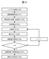
- FIG. 3 is a flowchart illustrating a procedure in which the charged particle beam device 1 observes the sample 122.
- the ON state of a transistor is the state in which charge is supplied to the gate part up to the gate voltage when a specified current flows between the source and drain
- the OFF state of the transistor is the state in which the gate part is supplied with charge up to the gate voltage when a specified current flows between the source and drain. Defined as a state in which the voltage due to charging is equal to or lower than the gate threshold voltage.
- the control messenger unit 147 determines the type, pattern, and inspection items of the device to be inspected.
- the device type and device pattern data may be specified from CAD data or information obtained by actually observing a SEM image of the observation position.
- the control messenger unit 147 specifies the location of the device pattern to be observed, the field of view size, the number of chips to be inspected, etc. (observation range) from the device pattern and chip layout.
- the control messenger unit 147 sets the range of the amount of charge to be injected and the conditions for light irradiation.
- the irradiation energy, minimum and maximum values of charge, and step amount of the electron beam to be injected to the specified pattern are determined.
- the electron beam conditions for injecting into the pattern and the conditions for observing the electron beam do not need to be the same.
- These electron beams may be output from the same electron source and electron optical system, or may be output from different electron sources and optical systems. Alternatively, the electron beam output from one electron source may be divided into a plurality of electron beams, and the electron beams may be controlled and irradiated individually.
- Step S102 Supplement
- recommended light irradiation conditions are set according to the inspection items input and selected in S100.
- the wavelength, irradiation amount, and irradiation timing of light calculated by the sequence control unit 151 are set according to the inspection items and device inspection range set by the measurement item setting unit 152. It is output to the control section 146. If the conditions are sufficient, the user checks, for example, a "confirm light condition” button on the GUI. If correction is necessary, the light irradiation conditions are corrected using the light condition input section displayed on the GUI, and when the light conditions are determined, the "confirm light condition” button is pressed.
- the light control unit 146 controls the light irradiation conditions according to the light conditions determined in "Light condition determination".
- the light control unit 146 stabilizes or equalizes the initial charging state of the sample 122 by irradiating the sample 122 with light, and controls the potential. For example, when transistors are formed in a grid pattern on the sample 122 (semiconductor material), the observation position is first scanned along the X direction, and the ON/OFF state of the transistor at each observation position is measured (the observation image is A specific example of measuring the ON/OFF state based on this will be described later). Next, the observation position is moved by one line in the Y direction. The light control unit 146 irradiates only the drain (and source) with light that resets the charging state each time the observation position is moved by one line in the Y direction.
- the light control unit 146 may emit light to reset the charged state of the gate when performing this step for the first time. Specific examples of light that resets only the drain and light that resets the gate will be described later.
- the electron optical system 11 injects charges into the sample 122 by irradiating the sample 122 with an electron beam.
- the charge injection conditions are those set in S102.
- the amount of charge injection is changed by the step width each time this step is performed. This step width is the one set in S102.
- the gate of the transistor is charged in accordance with the amount of charge injection, resulting in a state similar to that when a voltage is applied to the gate. By measuring at which stage the transistor turns on while changing the amount of charge injection, the ON/OFF characteristics (gate threshold voltage (Vth) characteristics) of the transistor can be measured.
- Vth gate threshold voltage
- Photoelectron emission by light irradiation may be used as a means for storing charge in the gate portion. If the material of the gate part is polysilicon, the gate can be removed by irradiating it with light of a wavelength that has an optical energy greater than the ionization energy of silicon, or by irradiating it with light that has a peak intensity that causes multiphoton excitation. Photoelectrons are emitted from the surface, resulting in positive charging. The gate may be turned on using this positive charge. Therefore, step S105 in FIG. 3 may be a means for irradiating light. The amount of charge stored may be controlled by optical parameters such as the amount of light irradiation, the irradiation time, the peak intensity, and the wavelength.
- the electron optical system 11 moves the field of view to the observation position and irradiates the electron beam under the electron optical conditions set in S103. Electrons emitted from the sample are detected by a detector 114.
- the calculation unit 148 uses the detection signal output by the detector 114 to generate an observation image at the observation position. The observed image is output to data or a GUI via the output unit 154 and display unit 155. If the observation position is the same as the charge injection position in S105, it is not necessary to move the irradiation position in S105 to S106. If they are not the same, the observation position may be moved by moving the stage, shifting the deflection of the electron beam, or the like.
- the calculation unit 148 acquires the brightness level of the observed image for each amount of charge injected into the sample 122 (S107). The calculation unit 148 performs this process for each observation position on the sample 122. Thereby, the in-plane distribution of the amount of injected charge and the brightness level can be obtained (S108). A specific example of the in-plane distribution will be described later.
- FIG. 4 is a diagram illustrating a method of controlling the charging state of a transistor formed on the sample 122 by light irradiation.
- a transistor includes a source, a gate, and a drain.
- This embodiment will be described using the structure of an n-type MOSFET (Metal Oxide Semiconductor Field Effect Transistor).
- An n-type MOSFET is formed by forming a silicon oxide film in a gate region on a p-type silicon substrate and forming a gate metal on the oxide film.
- an inversion layer is formed between the drain and the source.
- the gate is negatively charged and a negative voltage is applied to the gate portion.
- a method to control the positive or negative voltage applied to the gate part it is possible to control the accelerating voltage of the electron beam injected into the gate part, or to place an electrode directly above the sample and apply an electric field indirectly from the outside. Good too.
- a voltage may be applied by directly contacting the terminal with a terminal such as a prober.
- the electron beam may be applied to the entire pattern, or it may be applied to one point of the specified pattern coordinates where the transistor is formed. Good too.
- an irradiation method that simulates multiple operating states by using multiple electron beams to simultaneously or alternately irradiate negative voltage application conditions and positive voltage application conditions depending on the type of transistor during the same observation. May be implemented.
- the light control unit 146 removes the charges accumulated in the insulating film by irradiating light with wavelength 1 that is absorbed by the substrate material.
- the parts formed on the bonding structure are also reset at the same time because the substrate material is the same.
- the overall accumulated charge of the DRAM structure can be controlled or reset by irradiating light with a wavelength of 500 nm or less. is possible.
- the amount of charge accumulated in the gate portion can also be controlled. Furthermore, when controlling the charge in the gate portion, a wavelength that is directly absorbed by the gate insulating film may be irradiated. By resetting the charge on the gate, the transistor is turned off.
- Wavelength 2 is selected to eliminate the charge only on the portion formed on the junction. As a result, only the charges accumulated in the source and drain parts are reset while the charges are accumulated in the gate part (the gate part remains ON).
- the light control unit 146 can reset the charging state of the gate unit by irradiating light with wavelength 1.
- the charging state of the source portion and the drain portion can be reset by irradiating light with a wavelength of 2 every time the observation position is moved by one line in the Y direction. For example, if it is desired to observe characteristics such as breakdown voltage failure or recovery time of a junction, it is sufficient to irradiate wavelength 2 and then obtain a detection signal from the detector 114. If you want to observe the ON/OFF characteristics of the gate part (how much applied voltage, ie, the amount of charge injected, turns it on) or if you want to reset the entire transistor, wavelength 1 may be used.
- the secondary signal level detected by the detector 114 (that is, the brightness level of the observed image at the observation position) differs depending on whether the transistor is in the ON state. Therefore, the ON/OFF state of the transistor can be obtained based on the detection signal level or the pixel value of the observed image. According to this, the calculation unit 148 can measure the ON/OFF characteristics of the transistor.
- FIG. 5 is an example of the in-plane distribution created by the calculation unit 148 in S108.
- the detection signal from the detector 114 is acquired for each observation position while changing the amount of charge injected into the sample 122, the relationship between the amount of charge injected and the detection signal as shown in the lower diagram of FIG. can be obtained by position.
- an in-plane distribution as shown in the upper diagram of FIG. 5 is obtained.
- the detection signal quickly decreases.
- the detection signal decreases slowly with respect to the increase in the amount of injected charge.
- Such a difference is due to the fact that the characteristics of the transistor's transition between ON and OFF states when the amount of injected charge (that is, the voltage applied to the gate part) is gradually increased differs for each semiconductor chip formed on the sample 122. caused by.
- the in-plane distribution represents the distribution of such differences in characteristics.
- the in-plane distribution as shown in FIG. 5 can be obtained without necessarily obtaining an observation image of the sample 122. That is, if the detection signal level from the detector 114 is acquired for each amount of injected charge, the characteristics shown in the lower diagram of FIG. 5 can be obtained, so it is sufficient to create the in-plane distribution using this. For example, when obtaining an in-plane distribution as shown in FIG. 5 only for the drain portion of a transistor, it is sufficient to obtain the detection signal level when the drain portion is irradiated with an observation electron beam. By obtaining the in-plane distribution without generating observation images, measurement throughput can be ensured. For example, in the middle of the manufacturing process, the in-plane distribution as shown in FIG. 5 can be quickly obtained without stopping the process.
- the charged particle beam device 1 has a wavelength 1 that initializes the charged state of the gate portion of the transistor formed on the sample 122, and a wavelength 2 that initializes the charged state of only the drain portion and the source portion.
- the ON/OFF characteristics gate threshold voltage (Vth) characteristics
- Vth gate threshold voltage
- FIG. 6 is a diagram illustrating an operation example when the charged particle beam device 1 measures the parasitic capacitance between the gates of transistors.
- two transistors are connected so that their sources or drains are common (in FIG. 6, their source terminals are common).
- the charged particle beam device 1 can measure the parasitic capacitance between the gate terminals (portion indicated by the dotted line in FIG. 6) in FIG. 6 by the following procedure.
- the configuration of the charged particle beam device 1 is similar to that of the first embodiment.
- the control message section 147 irradiates the sample 122 with an electron beam so as to turn on only the gate of one of the transistors. As a result, a sufficient amount of charge is injected into the gate section on the right side of FIG. 6, for example, to turn it on. At this time, if the parasitic capacitance between the gate terminals is sufficiently small, only the transistor into which charge is injected becomes conductive. On the other hand, if the parasitic capacitance exceeds a certain reference value, charge is also injected into the other gate via the parasitic capacitance, thereby making the other transistor conductive.
- the conduction of a transistor can be detected by the detection signal level when the observation electron beam is irradiated to the transistor. That is, a detection signal from a transistor in a conductive state and a detection signal from a transistor in a non-conductive state have different signal levels.
- the calculation unit 148 can measure whether the parasitic capacitance shown by the dotted line in FIG. 6 is greater than or equal to the reference value based on the detection signal level in each transistor in the above procedure.
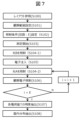
- FIG. 7 shows an example of a sequence in which electron beams and light are irradiated to calculate parasitic capacitance.
- the parasitic capacitance is measured by observing the time constant of the relaxation process of the injected charge. For example, the irradiation interval of the electron beam is changed, and the electrons emitted at that time are acquired by the detector 114.
- the time constant is small, so the time it takes for the stored charge to be discharged is shortened.
- the parasitic capacitance is large, the time constant becomes long, so by acquiring the brightness of the observed image of the gate at each electron beam irradiation interval, it is possible to calculate the parasitic capacitance between the gates. Steps similar to those in FIG. 3 are given the same step numbers, and the points different from FIG. 3 will be mainly explained below.
- a detection signal is acquired while varying the irradiation interval (interval step of the GUI described later) and current amount (irradiation current amount or pulse electron width) of the electron beam irradiated in observation electron irradiation (S106). , calculate the parasitic capacitance.
- step S104-1 the potential state of the entire transistor is made uniform, and in step S105, charge is injected into one gate portion.
- the observation position is moved to the drain portion formed by a switch such as a junction, and only the drain portion formed by the junction structure is reset in step S104-2.
- a detection signal is acquired while varying the irradiation interval (interval step of the GUI described later) and current amount (irradiation current amount or pulse electron width) of the electron beam irradiated by observation electron irradiation (S106). By doing so, the parasitic capacitance is calculated.
- the sample 122 is irradiated with the light set in step S104-2 each time the conditions such as the irradiation interval change.
- the charged particle beam device 1 has a wavelength 1 that initializes the charged state of the gate portion of the transistor formed on the sample 122, and a wavelength 2 that initializes the charged state of only the drain portion and the source portion.
- the parasitic capacitance between the wiring to the transistor is measured.
- the parasitic capacitance between wirings can be measured using light irradiation and charged particle beam irradiation without connecting measurement equipment such as electrical probes to transistors, and the distance between wirings and the quality of the insulating film can be measured. can be evaluated indirectly.
- FIG. 8 is an example of a user interface presented by the calculation unit 148 via the display unit 155.
- the user interface can present, for example, the following: (a) a charged particle beam irradiation condition input section for inputting irradiation conditions for electron beams (for both observation and charge injection); (b) a section for inputting electron beam irradiation conditions; Light irradiation condition input section for inputting irradiation conditions; (c) Observation image of sample 122; (d) Inspection results of sample 122 (transistor); (e) In-plane distribution in Figure 5 (distribution image in the upper row of Figure 5 and (at least one of the graphs below).
- control messenger section 147 executes the measurement sequence described in FIGS. 3 to 4 (or FIG. 6) by controlling each section according to the specified input.
- the in-plane distribution shown in FIG. 5 can be generated using the detection signal level without necessarily generating an observation image of the sample 122.
- the information used to measure the sample 122 it may be possible to switch between using only the detection signal level or generating an observation image. For example, the user may be able to specify on the GUI whether or not to generate an observation image.
- the light irradiation conditions for wavelength 1 and wavelength 2 explained in FIG. 4 can be switched based on whether or not a designated part of the sample 122 absorbs, so it is not necessarily necessary to switch the wavelength. Good too. For example, if whether or not the irradiated area absorbs the light depends on the light output, output switching may be used instead of wavelength switching. Furthermore, these may be combined.
- control messenger section 147 and the calculation section 148 have been described as separate functional sections, but they may be configured as an integrated control section.
- the control system 14 and the operation system 15 can be configured by hardware such as a circuit device that implements these functions, or can be configured by using software that implements these functions as a CPU (Central Processing System). It can also be configured by being executed by an arithmetic device such as a unit.
- CPU Central Processing System
Landscapes
- Analytical Chemistry (AREA)
- Chemical & Material Sciences (AREA)
- Physics & Mathematics (AREA)
- Health & Medical Sciences (AREA)
- Spectroscopy & Molecular Physics (AREA)
- General Physics & Mathematics (AREA)
- Life Sciences & Earth Sciences (AREA)
- Biochemistry (AREA)
- General Health & Medical Sciences (AREA)
- Immunology (AREA)
- Pathology (AREA)
- Toxicology (AREA)
- Testing Or Measuring Of Semiconductors Or The Like (AREA)
- Analysing Materials By The Use Of Radiation (AREA)
Priority Applications (5)
| Application Number | Priority Date | Filing Date | Title |
|---|---|---|---|
| PCT/JP2022/021468 WO2023228338A1 (ja) | 2022-05-25 | 2022-05-25 | 荷電粒子線装置、計測方法 |
| JP2024522814A JP7792509B2 (ja) | 2022-05-25 | 2022-05-25 | 荷電粒子線装置、計測方法 |
| KR1020247032671A KR20240157726A (ko) | 2022-05-25 | 2022-05-25 | 하전 입자선 장치, 계측 방법 |
| US18/853,804 US20250232946A1 (en) | 2022-05-25 | 2022-05-25 | Charged particle beam device, and measurement method |
| TW112110066A TWI861767B (zh) | 2022-05-25 | 2023-03-17 | 帶電粒子線裝置,計測方法 |
Applications Claiming Priority (1)
| Application Number | Priority Date | Filing Date | Title |
|---|---|---|---|
| PCT/JP2022/021468 WO2023228338A1 (ja) | 2022-05-25 | 2022-05-25 | 荷電粒子線装置、計測方法 |
Publications (1)
| Publication Number | Publication Date |
|---|---|
| WO2023228338A1 true WO2023228338A1 (ja) | 2023-11-30 |
Family
ID=88918739
Family Applications (1)
| Application Number | Title | Priority Date | Filing Date |
|---|---|---|---|
| PCT/JP2022/021468 Ceased WO2023228338A1 (ja) | 2022-05-25 | 2022-05-25 | 荷電粒子線装置、計測方法 |
Country Status (5)
| Country | Link |
|---|---|
| US (1) | US20250232946A1 (https=) |
| JP (1) | JP7792509B2 (https=) |
| KR (1) | KR20240157726A (https=) |
| TW (1) | TWI861767B (https=) |
| WO (1) | WO2023228338A1 (https=) |
Citations (5)
| Publication number | Priority date | Publication date | Assignee | Title |
|---|---|---|---|---|
| JPS6213619B2 (https=) * | 1978-11-11 | 1987-03-27 | Kogyo Gijutsu Incho | |
| US5430305A (en) * | 1994-04-08 | 1995-07-04 | The United States Of America As Represented By The United States Department Of Energy | Light-induced voltage alteration for integrated circuit analysis |
| JP2005108984A (ja) * | 2003-09-29 | 2005-04-21 | Renesas Technology Corp | 半導体装置の検査方法および半導体装置の製造方法 |
| JP2009246012A (ja) * | 2008-03-28 | 2009-10-22 | Hitachi High-Technologies Corp | 帯電電位測定方法、及び荷電粒子顕微鏡 |
| JP2014135314A (ja) * | 2013-01-08 | 2014-07-24 | Renesas Electronics Corp | 半導体装置の不良解析方法 |
Family Cites Families (2)
| Publication number | Priority date | Publication date | Assignee | Title |
|---|---|---|---|---|
| US7205539B1 (en) | 2005-03-10 | 2007-04-17 | Kla-Tencor Technologies Corporation | Sample charging control in charged-particle systems |
| WO2022091180A1 (ja) * | 2020-10-26 | 2022-05-05 | 株式会社日立ハイテク | 荷電粒子線装置 |
-
2022
- 2022-05-25 WO PCT/JP2022/021468 patent/WO2023228338A1/ja not_active Ceased
- 2022-05-25 JP JP2024522814A patent/JP7792509B2/ja active Active
- 2022-05-25 KR KR1020247032671A patent/KR20240157726A/ko active Pending
- 2022-05-25 US US18/853,804 patent/US20250232946A1/en active Pending
-
2023
- 2023-03-17 TW TW112110066A patent/TWI861767B/zh active
Patent Citations (5)
| Publication number | Priority date | Publication date | Assignee | Title |
|---|---|---|---|---|
| JPS6213619B2 (https=) * | 1978-11-11 | 1987-03-27 | Kogyo Gijutsu Incho | |
| US5430305A (en) * | 1994-04-08 | 1995-07-04 | The United States Of America As Represented By The United States Department Of Energy | Light-induced voltage alteration for integrated circuit analysis |
| JP2005108984A (ja) * | 2003-09-29 | 2005-04-21 | Renesas Technology Corp | 半導体装置の検査方法および半導体装置の製造方法 |
| JP2009246012A (ja) * | 2008-03-28 | 2009-10-22 | Hitachi High-Technologies Corp | 帯電電位測定方法、及び荷電粒子顕微鏡 |
| JP2014135314A (ja) * | 2013-01-08 | 2014-07-24 | Renesas Electronics Corp | 半導体装置の不良解析方法 |
Also Published As
| Publication number | Publication date |
|---|---|
| KR20240157726A (ko) | 2024-11-01 |
| TW202346878A (zh) | 2023-12-01 |
| JPWO2023228338A1 (https=) | 2023-11-30 |
| JP7792509B2 (ja) | 2025-12-25 |
| TWI861767B (zh) | 2024-11-11 |
| US20250232946A1 (en) | 2025-07-17 |
Similar Documents
| Publication | Publication Date | Title |
|---|---|---|
| KR100653499B1 (ko) | 저전압 입자빔을 이용한 반도체 조사용 전압 콘트라스트방법 및 장치 | |
| US7022986B2 (en) | Apparatus and method for wafer pattern inspection | |
| TWI887833B (zh) | 帶電粒子束裝置之控制器 | |
| US8168950B2 (en) | Charged particle beam apparatus, and image generation method with charged particle beam apparatus | |
| JP4253576B2 (ja) | パターン欠陥検査方法及び検査装置 | |
| US20120091339A1 (en) | Charged-particle microscope device, and method of controlling charged-particle beams | |
| JP4001373B2 (ja) | 集積回路断線検査方法と装置 | |
| KR102794066B1 (ko) | 하전 입자선 장치 | |
| JP7488898B2 (ja) | 荷電粒子検査システムのビーム電流調整 | |
| JP7792509B2 (ja) | 荷電粒子線装置、計測方法 | |
| US7183546B2 (en) | System and method for voltage contrast analysis of a wafer | |
| JP4625375B2 (ja) | 検査装置 | |
| JP4178003B2 (ja) | 半導体回路パターンの検査装置 | |
| TWI463517B (zh) | 檢查物的高速放電的調變器、系統及方法 | |
| TWI845782B (zh) | 用於檢測一基板之裝置及方法 | |
| TWI911743B (zh) | 電子束應用裝置及時間常數計測方法 | |
| TWI914960B (zh) | 帶電粒子線裝置 | |
| JP2004347483A (ja) | 電子線を用いたパターン検査装置、及び、電子線を用いたパターン検査方法 | |
| JP2007128738A (ja) | 帯電制御装置及び帯電制御装置を備えた荷電粒子線応用装置 | |
| JP7304624B2 (ja) | 電子顕微鏡 | |
| TW202531293A (zh) | 用於在裝置製造期間非接觸式量測能量障壁之系統及方法 | |
| JPH10294344A (ja) | 電子ビームテスタを用いた配線の欠陥検出方法および電子ビームテスタ | |
| Nishitani et al. | High-speed modulation of probe current using scanning electron microscope with photocathode technology | |
| WO2024029060A1 (ja) | 試料測定装置 | |
| WO2025262940A1 (ja) | 荷電粒子線装置および試料観察方法 |
Legal Events
| Date | Code | Title | Description |
|---|---|---|---|
| 121 | Ep: the epo has been informed by wipo that ep was designated in this application |
Ref document number: 22943740 Country of ref document: EP Kind code of ref document: A1 |
|
| ENP | Entry into the national phase |
Ref document number: 2024522814 Country of ref document: JP Kind code of ref document: A |
|
| ENP | Entry into the national phase |
Ref document number: 20247032671 Country of ref document: KR Kind code of ref document: A |
|
| WWE | Wipo information: entry into national phase |
Ref document number: 18853804 Country of ref document: US |
|
| NENP | Non-entry into the national phase |
Ref country code: DE |
|
| 122 | Ep: pct application non-entry in european phase |
Ref document number: 22943740 Country of ref document: EP Kind code of ref document: A1 |
|
| WWP | Wipo information: published in national office |
Ref document number: 18853804 Country of ref document: US |