WO2023218279A1 - 半導体装置 - Google Patents
半導体装置 Download PDFInfo
- Publication number
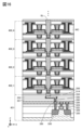
- WO2023218279A1 WO2023218279A1 PCT/IB2023/054418 IB2023054418W WO2023218279A1 WO 2023218279 A1 WO2023218279 A1 WO 2023218279A1 IB 2023054418 W IB2023054418 W IB 2023054418W WO 2023218279 A1 WO2023218279 A1 WO 2023218279A1
- Authority
- WO
- WIPO (PCT)
- Prior art keywords
- circuit
- delay
- signal
- function
- layer
- Prior art date
- Legal status (The legal status is an assumption and is not a legal conclusion. Google has not performed a legal analysis and makes no representation as to the accuracy of the status listed.)
- Ceased
Links
Images














Classifications
-
- H—ELECTRICITY
- H10—SEMICONDUCTOR DEVICES; ELECTRIC SOLID-STATE DEVICES NOT OTHERWISE PROVIDED FOR
- H10B—ELECTRONIC MEMORY DEVICES
- H10B12/00—Dynamic random access memory [DRAM] devices
-
- G—PHYSICS
- G06—COMPUTING OR CALCULATING; COUNTING
- G06F—ELECTRIC DIGITAL DATA PROCESSING
- G06F12/00—Accessing, addressing or allocating within memory systems or architectures
-
- G—PHYSICS
- G06—COMPUTING OR CALCULATING; COUNTING
- G06F—ELECTRIC DIGITAL DATA PROCESSING
- G06F12/00—Accessing, addressing or allocating within memory systems or architectures
- G06F12/02—Addressing or allocation; Relocation
- G06F12/06—Addressing a physical block of locations, e.g. base addressing, module addressing, memory dedication
-
- G—PHYSICS
- G11—INFORMATION STORAGE
- G11C—STATIC STORES
- G11C11/00—Digital stores characterised by the use of particular electric or magnetic storage elements; Storage elements therefor
- G11C11/21—Digital stores characterised by the use of particular electric or magnetic storage elements; Storage elements therefor using electric elements
- G11C11/34—Digital stores characterised by the use of particular electric or magnetic storage elements; Storage elements therefor using electric elements using semiconductor devices
- G11C11/40—Digital stores characterised by the use of particular electric or magnetic storage elements; Storage elements therefor using electric elements using semiconductor devices using transistors
- G11C11/401—Digital stores characterised by the use of particular electric or magnetic storage elements; Storage elements therefor using electric elements using semiconductor devices using transistors forming cells needing refreshing or charge regeneration, i.e. dynamic cells
- G11C11/403—Digital stores characterised by the use of particular electric or magnetic storage elements; Storage elements therefor using electric elements using semiconductor devices using transistors forming cells needing refreshing or charge regeneration, i.e. dynamic cells with charge regeneration common to a multiplicity of memory cells, i.e. external refresh
- G11C11/405—Digital stores characterised by the use of particular electric or magnetic storage elements; Storage elements therefor using electric elements using semiconductor devices using transistors forming cells needing refreshing or charge regeneration, i.e. dynamic cells with charge regeneration common to a multiplicity of memory cells, i.e. external refresh with three charge-transfer gates, e.g. MOS transistors, per cell
-
- G—PHYSICS
- G11—INFORMATION STORAGE
- G11C—STATIC STORES
- G11C11/00—Digital stores characterised by the use of particular electric or magnetic storage elements; Storage elements therefor
- G11C11/21—Digital stores characterised by the use of particular electric or magnetic storage elements; Storage elements therefor using electric elements
- G11C11/34—Digital stores characterised by the use of particular electric or magnetic storage elements; Storage elements therefor using electric elements using semiconductor devices
- G11C11/40—Digital stores characterised by the use of particular electric or magnetic storage elements; Storage elements therefor using electric elements using semiconductor devices using transistors
- G11C11/401—Digital stores characterised by the use of particular electric or magnetic storage elements; Storage elements therefor using electric elements using semiconductor devices using transistors forming cells needing refreshing or charge regeneration, i.e. dynamic cells
- G11C11/4063—Auxiliary circuits, e.g. for addressing, decoding, driving, writing, sensing or timing
- G11C11/407—Auxiliary circuits, e.g. for addressing, decoding, driving, writing, sensing or timing for memory cells of the field-effect type
- G11C11/4076—Timing circuits
-
- G—PHYSICS
- G11—INFORMATION STORAGE
- G11C—STATIC STORES
- G11C11/00—Digital stores characterised by the use of particular electric or magnetic storage elements; Storage elements therefor
- G11C11/21—Digital stores characterised by the use of particular electric or magnetic storage elements; Storage elements therefor using electric elements
- G11C11/34—Digital stores characterised by the use of particular electric or magnetic storage elements; Storage elements therefor using electric elements using semiconductor devices
- G11C11/40—Digital stores characterised by the use of particular electric or magnetic storage elements; Storage elements therefor using electric elements using semiconductor devices using transistors
- G11C11/401—Digital stores characterised by the use of particular electric or magnetic storage elements; Storage elements therefor using electric elements using semiconductor devices using transistors forming cells needing refreshing or charge regeneration, i.e. dynamic cells
- G11C11/4063—Auxiliary circuits, e.g. for addressing, decoding, driving, writing, sensing or timing
- G11C11/407—Auxiliary circuits, e.g. for addressing, decoding, driving, writing, sensing or timing for memory cells of the field-effect type
- G11C11/409—Read-write [R-W] circuits
- G11C11/4096—Input/output [I/O] data management or control circuits, e.g. reading or writing circuits, I/O drivers or bit-line switches
-
- G—PHYSICS
- G11—INFORMATION STORAGE
- G11C—STATIC STORES
- G11C5/00—Details of stores covered by group G11C11/00
- G11C5/02—Disposition of storage elements, e.g. in the form of a matrix array
- G11C5/04—Supports for storage elements, e.g. memory modules; Mounting or fixing of storage elements on such supports
-
- G—PHYSICS
- G11—INFORMATION STORAGE
- G11C—STATIC STORES
- G11C5/00—Details of stores covered by group G11C11/00
- G11C5/06—Arrangements for interconnecting storage elements electrically, e.g. by wiring
-
- G—PHYSICS
- G11—INFORMATION STORAGE
- G11C—STATIC STORES
- G11C7/00—Arrangements for writing information into, or reading information out from, a digital store
- G11C7/12—Bit line control circuits, e.g. drivers, boosters, pull-up circuits, pull-down circuits, precharging circuits, equalising circuits, for bit lines
-
- G—PHYSICS
- G11—INFORMATION STORAGE
- G11C—STATIC STORES
- G11C7/00—Arrangements for writing information into, or reading information out from, a digital store
- G11C7/22—Read-write [R-W] timing or clocking circuits; Read-write [R-W] control signal generators or management
-
- H—ELECTRICITY
- H10—SEMICONDUCTOR DEVICES; ELECTRIC SOLID-STATE DEVICES NOT OTHERWISE PROVIDED FOR
- H10B—ELECTRONIC MEMORY DEVICES
- H10B41/00—Electrically erasable-and-programmable ROM [EEPROM] devices comprising floating gates
- H10B41/70—Electrically erasable-and-programmable ROM [EEPROM] devices comprising floating gates the floating gate being an electrode shared by two or more components
-
- H—ELECTRICITY
- H10—SEMICONDUCTOR DEVICES; ELECTRIC SOLID-STATE DEVICES NOT OTHERWISE PROVIDED FOR
- H10B—ELECTRONIC MEMORY DEVICES
- H10B80/00—Assemblies of multiple devices comprising at least one memory device covered by this subclass
-
- H—ELECTRICITY
- H10—SEMICONDUCTOR DEVICES; ELECTRIC SOLID-STATE DEVICES NOT OTHERWISE PROVIDED FOR
- H10D—INORGANIC ELECTRIC SEMICONDUCTOR DEVICES
- H10D30/00—Field-effect transistors [FET]
- H10D30/01—Manufacture or treatment
- H10D30/021—Manufacture or treatment of FETs having insulated gates [IGFET]
-
- H—ELECTRICITY
- H10—SEMICONDUCTOR DEVICES; ELECTRIC SOLID-STATE DEVICES NOT OTHERWISE PROVIDED FOR
- H10D—INORGANIC ELECTRIC SEMICONDUCTOR DEVICES
- H10D30/00—Field-effect transistors [FET]
- H10D30/60—Insulated-gate field-effect transistors [IGFET]
- H10D30/67—Thin-film transistors [TFT]
-
- H—ELECTRICITY
- H10—SEMICONDUCTOR DEVICES; ELECTRIC SOLID-STATE DEVICES NOT OTHERWISE PROVIDED FOR
- H10D—INORGANIC ELECTRIC SEMICONDUCTOR DEVICES
- H10D30/00—Field-effect transistors [FET]
- H10D30/60—Insulated-gate field-effect transistors [IGFET]
- H10D30/68—Floating-gate IGFETs
-
- H—ELECTRICITY
- H10—SEMICONDUCTOR DEVICES; ELECTRIC SOLID-STATE DEVICES NOT OTHERWISE PROVIDED FOR
- H10D—INORGANIC ELECTRIC SEMICONDUCTOR DEVICES
- H10D30/00—Field-effect transistors [FET]
- H10D30/60—Insulated-gate field-effect transistors [IGFET]
- H10D30/69—IGFETs having charge trapping gate insulators, e.g. MNOS transistors
-
- H—ELECTRICITY
- H10—SEMICONDUCTOR DEVICES; ELECTRIC SOLID-STATE DEVICES NOT OTHERWISE PROVIDED FOR
- H10D—INORGANIC ELECTRIC SEMICONDUCTOR DEVICES
- H10D84/00—Integrated devices formed in or on semiconductor substrates that comprise only semiconducting layers, e.g. on Si wafers or on GaAs-on-Si wafers
-
- H—ELECTRICITY
- H10—SEMICONDUCTOR DEVICES; ELECTRIC SOLID-STATE DEVICES NOT OTHERWISE PROVIDED FOR
- H10D—INORGANIC ELECTRIC SEMICONDUCTOR DEVICES
- H10D84/00—Integrated devices formed in or on semiconductor substrates that comprise only semiconducting layers, e.g. on Si wafers or on GaAs-on-Si wafers
- H10D84/01—Manufacture or treatment
- H10D84/0123—Integrating together multiple components covered by H10D12/00 or H10D30/00, e.g. integrating multiple IGBTs
- H10D84/0126—Integrating together multiple components covered by H10D12/00 or H10D30/00, e.g. integrating multiple IGBTs the components including insulated gates, e.g. IGFETs
-
- H—ELECTRICITY
- H10—SEMICONDUCTOR DEVICES; ELECTRIC SOLID-STATE DEVICES NOT OTHERWISE PROVIDED FOR
- H10D—INORGANIC ELECTRIC SEMICONDUCTOR DEVICES
- H10D84/00—Integrated devices formed in or on semiconductor substrates that comprise only semiconducting layers, e.g. on Si wafers or on GaAs-on-Si wafers
- H10D84/01—Manufacture or treatment
- H10D84/02—Manufacture or treatment characterised by using material-based technologies
- H10D84/03—Manufacture or treatment characterised by using material-based technologies using Group IV technology, e.g. silicon technology or silicon-carbide [SiC] technology
- H10D84/038—Manufacture or treatment characterised by using material-based technologies using Group IV technology, e.g. silicon technology or silicon-carbide [SiC] technology using silicon technology, e.g. SiGe
-
- H—ELECTRICITY
- H10—SEMICONDUCTOR DEVICES; ELECTRIC SOLID-STATE DEVICES NOT OTHERWISE PROVIDED FOR
- H10W—GENERIC PACKAGES, INTERCONNECTIONS, CONNECTORS OR OTHER CONSTRUCTIONAL DETAILS OF DEVICES COVERED BY CLASS H10
- H10W90/00—Package configurations
-
- H—ELECTRICITY
- H10—SEMICONDUCTOR DEVICES; ELECTRIC SOLID-STATE DEVICES NOT OTHERWISE PROVIDED FOR
- H10W—GENERIC PACKAGES, INTERCONNECTIONS, CONNECTORS OR OTHER CONSTRUCTIONAL DETAILS OF DEVICES COVERED BY CLASS H10
- H10W90/00—Package configurations
- H10W90/20—Configurations of stacked chips
- H10W90/297—Configurations of stacked chips characterised by the through-semiconductor vias [TSVs] in the stacked chips
-
- H—ELECTRICITY
- H10—SEMICONDUCTOR DEVICES; ELECTRIC SOLID-STATE DEVICES NOT OTHERWISE PROVIDED FOR
- H10W—GENERIC PACKAGES, INTERCONNECTIONS, CONNECTORS OR OTHER CONSTRUCTIONAL DETAILS OF DEVICES COVERED BY CLASS H10
- H10W90/00—Package configurations
- H10W90/701—Package configurations characterised by the relative positions of pads or connectors relative to package parts
- H10W90/721—Package configurations characterised by the relative positions of pads or connectors relative to package parts of bump connectors
- H10W90/722—Package configurations characterised by the relative positions of pads or connectors relative to package parts of bump connectors between stacked chips
Definitions
- One embodiment of the present invention relates to a semiconductor device.
- One embodiment of the present invention relates to a method for driving a semiconductor device.
- One aspect of the present invention relates to a storage device.
- One aspect of the present invention relates to a method for driving a storage device.
- One embodiment of the present invention relates to electronic equipment.
- one embodiment of the present invention is not limited to the above technical field.
- the technical field of the invention disclosed in this specification and the like relates to products, methods, or manufacturing methods.
- one aspect of the present invention relates to a process, machine, manufacture, or composition of matter. Therefore, the technical fields of one embodiment of the present invention more specifically disclosed in this specification include semiconductor devices, display devices, light-emitting devices, power storage devices, storage devices, driving methods thereof, or manufacturing methods thereof; can be cited as an example.
- the distance between the drive circuit and the memory cell array is The wiring distance differs depending on the hierarchy of the memory cell array. Specifically, the higher the memory cell array is provided, the longer the wiring distance from the drive circuit to the memory cell array becomes. The longer the wiring distance, the greater the wiring resistance, so the time from when the drive circuit generates a signal until the signal is supplied to the memory cell array, and when the data is read from the memory cell array, the data is transferred to the drive circuit. It may take longer to receive the product.
- reading data held in memory cells in an upper hierarchy may be slower than reading data held in memory cells in a lower hierarchy. This may cause the semiconductor device to malfunction.
- An object of one embodiment of the present invention is to provide a highly reliable semiconductor device.
- an object of one embodiment of the present invention is to provide a semiconductor device with a large storage capacity.
- an object of one embodiment of the present invention is to provide a semiconductor device with high storage density.
- an object of one embodiment of the present invention is to provide a small-sized semiconductor device.
- an object of one embodiment of the present invention is to provide a semiconductor device with low power consumption.
- an object of one embodiment of the present invention is to provide a novel semiconductor device.
- One aspect of the present invention includes a first layer, a second layer on the first layer, and a third layer on the second layer, and the first layer is configured to generate a delayed signal.
- the second layer includes a first delay adding circuit, a first storage section in which first memory cells are arranged in a matrix
- a third layer includes a first delay adding circuit and a first storage section in which first memory cells are arranged in a matrix.
- the layer includes a second delay adding circuit and a second storage section in which second memory cells are arranged in a matrix
- the delay signal generating circuit has a first delay adding circuit and a second storage section in which second memory cells are arranged in a matrix.
- the circuit has a function of generating a delayed signal representing the second delay time and supplying it to the first delay adding circuit, and a function of generating a second delayed signal representing the second delay time and supplying it to the second delay adding circuit.
- the circuit has a function of generating a row selection signal for selecting a first or second memory cell to perform a read operation and supplying it to the first or second delay adding circuit, and the first delay adding circuit , has a function of supplying the row selection signal supplied to the first delay adding circuit to the first storage unit after the first delay time has elapsed, and the second delay adding circuit has a function of supplying the row selection signal supplied to the first delay adding circuit to the first storage section
- the semiconductor device has a function of supplying the row selection signal supplied to the circuit to the second storage section after a second delay time has elapsed, and the first delay time is longer than the second delay time.
- one aspect of the invention has a first layer, a second layer on the first layer, and a third layer on the second layer, wherein the first layer is selected from
- the second layer includes a signal generation circuit, a delayed signal generation circuit, and a row circuit
- the second layer includes a first selection circuit, a first delay addition circuit, and a first memory cell arranged in a matrix.
- the third layer has a second storage section in which a second selection circuit, a second delay addition circuit, and a second memory cell are arranged in a matrix.
- the selection signal generation circuit has a function of generating a selection signal and supplying it to the delay signal generation circuit, the first selection circuit, and the second selection circuit, and the delay signal generation circuit includes:
- the delay signal generation circuit has a function of generating a first delay signal representing the first delay time and a function of generating a second delay signal representing the second delay time, and the delay signal generation circuit generates the second delay signal based on the selection signal.
- the row circuit has a function of outputting one of the first delay signal or the second delay signal and supplying it to the first delay adding circuit and the second delay adding circuit, or has a function of generating a row selection signal for selecting the second memory cell, and the row circuit has a function of supplying the row selection signal to the first selection circuit and the second selection circuit,
- the first selection circuit has a function of supplying a row selection signal to the first delay addition circuit when the delay signal generation circuit outputs the first delay signal
- the second selection circuit has a function of supplying the row selection signal to the first delay addition circuit when the delay signal generation circuit outputs the first delay signal.
- the row selection signal has a function of supplying the second delay addition circuit to the second delay addition circuit
- the first delay addition circuit has a function of supplying the row selection signal to the second delay addition circuit.
- the second delay adding circuit has a function of supplying the row selection signal to the first storage section after the first delay time has elapsed, and the second delay adding circuit supplies the row selection signal supplied to the second delay adding circuit to the first storage section.
- the first delay time is longer than the second delay time.
- the first layer has a reference signal generation circuit
- the second layer has a first buffer circuit
- the third layer has a second buffer circuit
- the reference signal generation circuit has a function of generating a reference signal and supplying it to the delayed signal generation circuit, the first buffer circuit, and the second buffer circuit
- the first buffer circuit has a function of generating a reference signal and supplying it to the delayed signal generation circuit, the first buffer circuit, and the second buffer circuit.
- the second buffer circuit has a function of supplying the supplied reference signal to the delayed signal generation circuit as a first delay time detection signal
- the second buffer circuit converts the supplied reference signal to the second buffer circuit as a first delay time detection signal.
- the delay signal generation circuit has a function of supplying the delay time detection signal to the delay signal generation circuit, and the delay signal generation circuit has the function of supplying the signal as a delay time detection signal to the delay signal generation circuit.
- the delayed signal generating circuit has a function of generating a first digital signal representing the difference between the first time and the second time, and generating a first delayed signal based on the first digital signal. It may have a function of generating a second digital signal representing the difference between the third time when the delay time detection signal is input and generating the second delay signal based on the second digital signal.
- the delayed signal generation circuit includes a first inverter circuit and a second inverter circuit, and the first inverter circuit supplies the first digital signal to the first inverter circuit.
- the second inverter circuit has a function of generating a first delayed signal when the second digital signal is supplied to the second inverter circuit. It may also have the function of
- the delayed signal generation circuit has a first transistor, the first memory cell has a second transistor, and the second memory cell has a third transistor,
- the first transistor may have silicon in its channel formation region, and the second transistor and the third transistor may have metal oxide in their channel formation regions.
- one embodiment of the present invention includes a first block and a second block, and the first block includes a first layer, a second layer on the first layer, and a second block. a third layer on the second layer, and the second block has a fourth layer, a fifth layer on the fourth layer, and a sixth layer on the fifth layer.
- the first layer has a first delay signal generation circuit and a first row circuit
- the second layer has a first delay addition circuit and a first memory cell.
- the third layer includes a second delay adding circuit and a second memory section in which second memory cells are arranged in a matrix.
- the fourth layer has a second delay signal generation circuit and a second row circuit
- the fifth layer has a third delay addition circuit and a third memory cell.
- the sixth layer includes a fourth delay adding circuit and a fourth memory section in which fourth memory cells are arranged in a matrix.
- the first delay signal generation circuit has a function of generating a first delay signal representing a first delay time and supplying it to the first delay addition circuit, and a function of generating a first delay signal representing a first delay time and supplying the first delay signal to the first delay addition circuit.
- the second delay signal generation circuit generates a third delay signal representing a third delay time and supplies it to a second delay adding circuit.
- the first row circuit has a function of supplying the delay signal to the delay adding circuit, and a function of generating a fourth delay signal representing the fourth delay time and supplying the fourth delay signal to the fourth delay adding circuit, and the first row circuit performs a read operation. It has a function of generating a first row selection signal for selecting a first or second memory cell and supplying it to the first or second delay adding circuit, and the second row circuit performs a read operation. It has a function of generating a second row selection signal for selecting the third or fourth memory cell and supplying it to the third or fourth delay adding circuit, and the first delay adding circuit selects the third or fourth memory cell.
- the second delay adding circuit has a function of supplying the first row selection signal supplied to the delay adding circuit to the first storage section after the first delay time has elapsed, and the second delay adding circuit
- the third delay adding circuit has a function of supplying the first row selection signal supplied to the second storage section after a second delay time has elapsed;
- the fourth delay adding circuit has a function of supplying the second row selection signal supplied to the fourth delay adding circuit to the third storage section after the third delay time has elapsed. has a function of supplying a row selection signal to a fourth storage unit after a fourth delay time has elapsed, the first delay time is longer than the second delay time, and the third delay time is longer than the second delay time.
- This semiconductor device has a longer delay time than No. 4.
- one embodiment of the present invention includes a first block and a second block, and the first block includes a first layer, a second layer on the first layer, and a second block. a third layer on the second layer, and the second block has a fourth layer, a fifth layer on the fourth layer, and a sixth layer on the fifth layer.
- the first layer has a first selection signal generation circuit, a first delay signal generation circuit, and a first row circuit
- the second layer has a first selection signal generation circuit.
- the third layer includes a second selection circuit, a first delay adding circuit, and a first storage section in which first memory cells are arranged in a matrix.
- the fourth layer includes a delay adding circuit and a second storage section in which second memory cells are arranged in a matrix
- the fourth layer includes a second selection signal generation circuit and a second delay signal generation circuit. and a second row circuit
- the fifth layer includes a third selection circuit, a third delay adding circuit, and a third memory in which third memory cells are arranged in a matrix
- the sixth layer has a fourth selection circuit, a fourth delay adding circuit, and a fourth storage section in which fourth memory cells are arranged in a matrix.
- the first selection signal generation circuit has a function of generating a first selection signal and supplying it to the first delay signal generation circuit, the first selection circuit, and the second selection circuit;
- the selection signal generation circuit has a function of generating a second selection signal and supplying it to the second delay signal generation circuit, the third selection circuit, and the fourth selection circuit, and the selection signal generation circuit has a function of generating a first delay signal representing a first delay time and a function of generating a second delay signal representing a second delay time, and the first delay signal generation circuit has a function of generating a first delay signal representing a first delay time, and a function of generating a second delay signal representing a second delay time.
- the delay signal generation circuit has a function of generating a third delay signal representing a third delay time, a function of generating a fourth delay signal representing a fourth delay time, and a function of generating a fourth delay signal representing a fourth delay time.
- the generation circuit has a function of outputting either the third delay signal or the fourth delay signal based on the second selection signal and supplying the output to the third delay addition circuit and the fourth delay addition circuit.
- the first row circuit has a function of generating a first row selection signal that selects the first or second memory cell to perform a read operation; It has a function of supplying a row selection signal to a first selection circuit and a second selection circuit, and the second row circuit selects a third or fourth memory cell to perform a read operation.
- the second row circuit has a function of supplying the second row selection signal to the third selection circuit and the fourth selection circuit, and The selection circuit has a function of supplying the first row selection signal to the first delay addition circuit when the first delay signal generation circuit outputs the first delay signal, and the second selection circuit has a function of supplying the first row selection signal to the first delay addition circuit.
- the third selection circuit has a function of supplying the first row selection signal to the second delay addition circuit when the first delay signal generation circuit outputs the second delay signal
- the third selection circuit has a function of supplying the first row selection signal to the second delay addition circuit.
- the fourth selection circuit has a function of supplying the second row selection signal to the third delay addition circuit, and the fourth selection circuit outputs the second delay signal.
- the generation circuit outputs the fourth delay signal, it has a function of supplying the second row selection signal to the fourth delay addition circuit, and the first delay addition circuit supplies the second row selection signal to the first delay addition circuit.
- the second delay adding circuit has a function of supplying the supplied first row selection signal to the first storage section after the first delay time has elapsed, and the second delay adding circuit has a function of supplying the supplied first row selection signal to the first storage section after the first delay time has elapsed.
- the third delay adding circuit has a function of supplying the first row selection signal to the second storage section after the second delay time has elapsed, and the third delay adding circuit has a function of supplying the first row selection signal to the second storage section after the second delay time has passed, and
- the fourth delay adding circuit has a function of supplying the row selection signal to the third storage unit after the third delay time has elapsed, and the fourth delay adding circuit receives the second row selection signal supplied to the fourth delay adding circuit.
- the first layer has a first reference signal generation circuit
- the second layer has a first buffer circuit
- the third layer has a second buffer circuit
- the fourth layer has a second reference signal generation circuit
- the fifth layer has a third buffer circuit
- the sixth layer has a fourth buffer circuit
- the first reference signal generation circuit has a function of generating a first reference signal and supplying it to the first delayed signal generation circuit, the first buffer circuit, and the second buffer circuit
- the signal generating circuit has a function of generating a second reference signal and supplying it to the second delayed signal generating circuit, the third buffer circuit, and the fourth buffer circuit.
- the second buffer circuit has a function of supplying the first reference signal supplied to the first buffer circuit to the first delay signal generation circuit as a first delay time detection signal
- the second buffer circuit The third buffer circuit has a function of supplying the first reference signal supplied to the third buffer circuit as a second delay time detection signal to the first delay signal generation circuit.
- the fourth buffer circuit has a function of supplying the second reference signal as a third delay time detection signal to the second delay signal generation circuit, and the fourth buffer circuit supplies the second reference signal as a third delay time detection signal to the second delay signal generation circuit.
- the first delay signal generation circuit has a function of supplying the signal as a fourth delay time detection signal to a second delay signal generation circuit, and the first delay signal generation circuit has a first time when the first reference signal is input, and It has a function of generating a first digital signal representing a difference between a second time at which the first delay time detection signal is input, and generating a first delay signal based on the first digital signal,
- the first delay signal generation circuit generates a second digital signal representing the difference between the first time and a third time at which the second delay time detection signal is input, and generates a second digital signal.
- the second delay signal generation circuit has a function of generating a second delay signal based on a third time when the second reference signal is input and a third time when the third delay time detection signal is input.
- the second delayed signal generating circuit has a function of generating a third digital signal representing the difference between the fourth time and the fourth time, and generating a third delayed signal based on the third digital signal. and a fourth time at which the fourth delay time detection signal is input, and generate a fourth delay signal based on the fourth digital signal. It may have.
- the first delayed signal generation circuit includes a first inverter circuit and a second inverter circuit
- the second delayed signal generation circuit includes a third inverter circuit and a second inverter circuit.
- 4 inverter circuits the first inverter circuit has a function of generating a first delayed signal when the first digital signal is supplied to the first inverter circuit
- the second The inverter circuit has a function of generating a second delayed signal when the second digital signal is supplied to the second inverter circuit
- the third inverter circuit has a function of generating a second delayed signal when the second digital signal is supplied to the second inverter circuit.
- the fourth inverter circuit has a function of generating the third delayed signal. It may have a function of generating 4 delayed signals.
- the first delayed signal generation circuit includes a first transistor, the first memory cell includes a second transistor, and the second memory cell includes a third transistor.
- the second delay signal generation circuit has a fourth transistor, the third memory cell has a fifth transistor, the fourth memory cell has a sixth transistor,
- the first transistor and the fourth transistor have silicon in the channel formation region, and the second transistor, the third transistor, the fifth transistor, and the sixth transistor have metal oxide in the channel formation region. It may have.
- the timing at which the first row circuit outputs the first row selection signal and the timing at which the second row circuit outputs the second row selection signal may be synchronized.
- a highly reliable semiconductor device can be provided.
- a semiconductor device with a large storage capacity can be provided.
- a semiconductor device with high storage density can be provided.
- a small-sized semiconductor device can be provided.
- a semiconductor device with low power consumption can be provided.
- a novel semiconductor device can be provided.
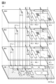
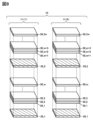
- FIG. 1 is a perspective view showing an example of the configuration of a semiconductor device.
- FIG. 2 is a perspective view showing a configuration example of a semiconductor device.
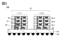
- FIG. 3 is a cross-sectional view showing a configuration example of a semiconductor device.
- FIG. 4 is a block diagram showing a configuration example of a semiconductor device.
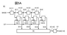
- FIG. 5A is a block diagram showing a configuration example of a semiconductor device.
- FIG. 5B is a timing chart showing an example of a method for driving a semiconductor device.
- FIG. 6 is a block diagram showing a configuration example of a semiconductor device.
- FIG. 7 is a circuit diagram showing a configuration example of a semiconductor device.
- FIG. 8A is a circuit diagram showing a configuration example of an inverter circuit.
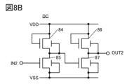
- FIG. 8B is a circuit diagram showing a configuration example of a delay circuit.
- FIG. 9 is a perspective view showing a configuration example of a semiconductor device.
- FIG. 10 is a perspective view showing a configuration example of a semiconductor device.
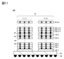
- FIG. 11 is a cross-sectional view showing a configuration example of a semiconductor device.
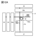
- FIG. 12A is a block diagram showing a configuration example of a semiconductor device.
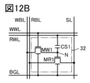
- FIG. 12B is a circuit diagram showing a configuration example of a memory cell.
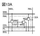
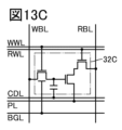
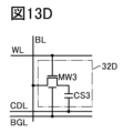
- 13A to 13D are circuit diagrams showing configuration examples of memory cells.
- FIG. 14 is a cross-sectional view showing a configuration example of a semiconductor device.
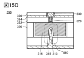
- 15A to 15C are cross-sectional views showing configuration examples of transistors.
- FIG. 16 is a cross-sectional view showing a configuration example of a semiconductor device.
- FIG. 17A is a cross-sectional view showing a configuration example of a semiconductor device.
- FIG. 17B is a circuit diagram showing a configuration example of a memory cell.
- FIG. 18 is a cross-sectional view showing a configuration example of a semiconductor device.
- FIG. 19A is a cross-sectional view showing a configuration example of a semiconductor device.
- FIG. 19B is a circuit diagram showing a configuration example of a memory cell.
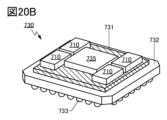
- 20A and 20B are diagrams showing an example of an electronic component.
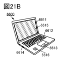
- FIG. 21A and FIG. 21B are diagrams showing an example of an electronic device.
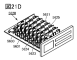
- FIGS. 21C to 21E are diagrams showing an example of a large-sized computer.
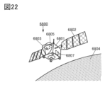
- FIG. 22 is a diagram showing an example of space equipment.
- FIG. 23 is a diagram illustrating an example of a storage system applicable to a data center.
- off-state current refers to a drain current when a transistor is in an off state (also referred to as a non-conducting state or a cutoff state).
- an off state is a state in which the voltage between the gate and source, V gs , is lower than the threshold voltage V th for n-channel transistors (higher than V th for p-channel transistors). means.
- metal oxide refers to a metal oxide in a broad sense. Metal oxides are classified into oxide insulators, oxide conductors (including transparent oxide conductors), oxide semiconductors (also referred to as oxide semiconductors or simply OS), and the like. For example, when a metal oxide is used in the active layer of a transistor, the metal oxide is sometimes called an oxide semiconductor. That is, when it is described as an OS transistor, it can be translated as a transistor including a metal oxide or an oxide semiconductor.
- a semiconductor device described in one embodiment of the present invention can be, for example, a memory device.
- One embodiment of the present invention relates to a semiconductor device having a plurality of blocks.
- a plurality of layers each having a storage section in which memory cells are arranged in a matrix are stacked on top of a layer having a drive circuit.
- the storage capacity per unit area can be increased, for example when the semiconductor device is viewed from above. Therefore, the storage density of the semiconductor device can be increased compared to the case where only one storage layer is provided. Further, the semiconductor device can be downsized while ensuring storage capacity. Note that since memory cells are arranged in a matrix in the storage section, the storage section is also referred to as a memory cell array.
- the drive circuit has a function of controlling writing and reading of data to and from memory cells.
- the wiring distance from the drive circuit to the memory cells differs depending on the level of the layer including the memory cells even if the memory cells are in the same row and column. Specifically, the higher the memory cell is provided, the longer the wiring distance from the drive circuit to the memory cell becomes. The longer the wiring distance, the greater the wiring resistance, so the time from when the drive circuit generates a signal until the signal is supplied to the memory cell, and when reading data from the memory cell, the data is transferred to the drive circuit. It may take longer to receive the product. Therefore, for example, even if it is necessary to simultaneously read data from a plurality of memory cells provided in different hierarchies of different blocks, the data may not be read simultaneously. Specifically, reading data held in memory cells in an upper hierarchy may be slower than reading data held in memory cells in a lower hierarchy. This may cause the semiconductor device to malfunction.
- a delay adding circuit is provided for each layer including memory cells.
- the signal generated by the drive circuit is supplied to the delay adding circuit.
- the signal supplied to the delay adding circuit is supplied to the memory cell after a predetermined time. Therefore, it can be said that the delay adding circuit has a function of adding a predetermined delay time to the signal generated by the drive circuit.
- the delay adding circuit provided at a lower level adds a longer delay time to the signal generated by the drive circuit.
- the delay adding circuit for example, after the driver circuit generates a signal, the signal is supplied to the memory cell, and data is output from the memory cell in response to the signal.
- the time required for reading can be made equal or approximately equal between layers having memory cells. Therefore, for example, data can be read simultaneously or approximately simultaneously from a plurality of memory cells provided in different hierarchies of different blocks. As described above, it is possible to suppress malfunctions of the semiconductor device and provide a highly reliable semiconductor device.
- the semiconductor device of one embodiment of the present invention can have high storage density and high reliability.
- FIG. 1 is a perspective view illustrating a configuration example of a semiconductor device 10, which is a semiconductor device of one embodiment of the present invention.
- the semiconductor device 10 can be, for example, a storage device.
- the semiconductor device 10 includes a block 11 ⁇ 1> and a block 11 ⁇ 2>.
- Block 11 ⁇ 1> and block 11 ⁇ 2> each include a layer 20 and layers 30_1 to 30_n (n is an integer of 2 or more).
- the layers 30_1 to 30_n are sequentially stacked on the layer 20.
- the layers 30 are shown as a layer 30_1, a layer 30_2, a layer 30_3, and a layer 30_n.
- the semiconductor device 10 may have three or more blocks 11. Further, the semiconductor device 10 may have only one block 11.
- layers with the same reference numerals are provided in the same hierarchy.
- the layer 20 of block 11 ⁇ 1> and the layer 20 of block 11 ⁇ 2> are provided in the same layer.
- the layer 30_1 of block 11 ⁇ 1> and the layer 30_1 of block 11 ⁇ 2> are provided in the same layer.
- layer 30_1 of block 11 ⁇ 1> and layer 30_n of block 11 ⁇ 1> are provided in different hierarchies.
- Memory cells (not shown) are arranged in a matrix in each of the layers 30_1 to 30_n.
- the layer 20 is provided with a drive circuit (not shown) that has the function of controlling writing and reading of data into the memory cells.
- data held in the memory cells of block 11 ⁇ 1> and data held in the memory cells of block 11 ⁇ 2> can be read in parallel.
- data held in a plurality of memory cells provided in mutually different blocks 11 can be read out in parallel.
- data can be read in parallel from a plurality of memory cells provided in layers 30 of different hierarchies between different blocks 11.
- data held in memory cells provided in layer 30_1 of block 11 ⁇ 1> and data held in memory cells provided in layer 30_3 of block 11 ⁇ 2> may be read in parallel. I can do it.
- FIG. 2 is a perspective view showing an example of the configuration of the block 11. Specifically, FIG. 2 shows an example of the structure of the layer 20, layer 30_1, layer 30_2, and layer 30_3. As shown in FIG. 2, layer 30_1 is provided on layer 20, layer 30_2 is provided on layer 30_1, and layer 30_3 is provided on layer 30_2.
- the layer 20 includes a reference signal generation circuit 21, a selection signal generation circuit 22, a delay signal generation circuit 23, a row circuit 24, a column circuit 25, and a sense amplifier circuit 27.
- the layer 30_1 includes a storage section 31_1, a selection circuit 33_1, a delay addition circuit 35a_1, a delay addition circuit 35b_1, and a buffer circuit 37_1, and memory cells 32_1 are arranged in a matrix in the storage section 31_1.
- the layer 30_2 includes a storage section 31_2, a selection circuit 33_2, a delay addition circuit 35a_2, a delay addition circuit 35b_2, and a buffer circuit 37_2, and memory cells 32_2 are arranged in a matrix in the storage section 31_2. .
- the layer 30_3 includes a storage section 31_3, a selection circuit 33_3, a delay addition circuit 35a_3, a delay addition circuit 35b_3, and a buffer circuit 37_3, and memory cells 32_3 are arranged in a matrix in the storage section 31_3. .
- the memory cell 32 is electrically connected to a delay adding circuit 35a for each row via a word line, and a delay adding circuit 35b and a sense amplifier circuit for each column via a bit line. It is electrically connected to 27.
- the circuit provided in the layer 20 and the circuit provided in the layer 30 are circuits for controlling the driving of the semiconductor device 10. Therefore, the circuit provided in layer 20 and the circuit provided in layer 30 can be said to be a drive circuit. Alternatively, among the circuits provided in the layer 20 and the circuits provided in the layer 30, the circuits excluding the memory cells 32 may be referred to as a drive circuit.
- the flow of signals or data between the components of the block 11 is indicated by arrows.
- the signal or data represented by the arrow is not limited to a 1-bit digital signal or digital data, but may be, for example, a 2-bit or more digital signal or digital data.
- the exchange of signals or data shown in FIG. 2 is just an example, and there are cases where signals or data can be exchanged between components that are not connected by arrows, for example. Further, signals or data may be exchanged between components connected by arrows in the direction opposite to the arrow. The same applies to cases other than those shown in FIG.
- the reference signal generation circuit 21 has a function of generating a reference signal BASE and supplying it to the delay signal generation circuit 23 and the buffer circuit 37.
- the reference signal BASE can be, for example, a 1-bit digital signal.
- the buffer circuit 37 has an input terminal and an output terminal, and has a function of supplying the reference signal BASE supplied to the input terminal to the delay signal generation circuit 23 as a delay time detection signal DT.
- the reference signal BASE supplied to the input terminal of the buffer circuit 37_1 is output as the delay time detection signal DT_1 from the output terminal of the buffer circuit 37_1, and is supplied to the delay signal generation circuit 23.
- the reference signal BASE supplied to the input terminal of the buffer circuit 37_2 is output as a delay time detection signal DT_2 from the output terminal of the buffer circuit 37_2, and is supplied to the delay signal generation circuit 23.
- the reference signal BASE supplied to the input terminal of the buffer circuit 37_3 is outputted from the output terminal of the buffer circuit 37_3 as a delay time detection signal DT_3, and is supplied to the delay signal generation circuit 23.
- the buffer circuit 37 may not be provided in the layer 30.
- the selection signal generation circuit 22 has a function of generating a selection signal SEL and supplying it to the delay signal generation circuit 23 and the selection circuit 33.
- the delay signal generation circuit 23 has a function of generating a delay signal DA based on the reference signal BASE and the delay time detection signal DT, and supplying it to the delay addition circuit 35a and the delay addition circuit 35b.
- the delay signal generation circuit 23 generates the delay signal DA based on the reference signal BASE and any one of the plurality of delay time detection signals DT, and, for example, all the delay adding circuits included in the block 11. 35a and the delay adding circuit 35b.
- the delay signal DA is a signal for determining time, and includes a first time when the reference signal BASE is supplied to the delay signal generation circuit 23 and a second time when the delay time detection signal DT is supplied to the delay signal generation circuit 23. It is generated based on the difference between the times of 2 and 2. Although details will be described later, the larger the difference in time, the shorter the time determined by the delay signal DA.
- the time difference refers to the absolute value of the time difference.
- the delay time detection signal DT used to generate the delay signal DA is selected by the selection signal SEL.
- the delay signal generation circuit 23 generates the delay signal DA using the reference signal BASE, the selection signal SEL, and any one of the delay time detection signals DT_1 to DT_3 selected by the selection signal SEL. do.
- the row circuit 24 has a function of generating a row selection signal RSEL and supplying it to the selection circuit 33.
- the row selection signal RSEL is a signal for selecting a memory cell 32 into which data is written or a memory cell 32 from which data is read out of the memory cells 32 arranged in a matrix.
- the row selection signal RSEL is a signal for selecting a row of memory cells 32 into which data is written or a row of memory cells 32 from which data is read.
- the row selection signal RSEL is supplied to all selection circuits 33 included in the block 11, for example.
- the row selection signal RSEL is supplied to the memory cell 32 via the aforementioned word line. Therefore, the row circuit 24 can be said to be a word line drive circuit.
- the column circuit 25 has a function of writing data DATAin into the memory cell 32 via the delay adding circuit 35b. Further, the column circuit 25 has a function of outputting data read from the memory cell 32 as data DATAout. Further, the column circuit 25 has a function of generating a precharge signal for precharging the bit line described above before reading data from the memory cell 32, and supplying the precharge signal to the delay adding circuit 35b.
- the row circuit 24 and the column circuit 25 have a function of controlling data writing to and reading from the memory cells 32.
- the sense amplifier circuit 27 has a function of amplifying data read from the memory cell 32.
- the column circuit 25 When reading data from the memory cell 32, first, the column circuit 25 generates a precharge signal as described above, thereby setting the potential of the bit line to the precharge potential. Next, the potential of the bit line is set to a potential corresponding to the data to be read. For example, when 1 bit of digital data is held in the memory cell 32, when reading data with a digital value of "1", the potential of the bit line is set to a data potential higher than the precharge potential, and the digital value becomes "0". When reading data, the potential of the bit line is set to a data potential lower than the precharge potential. Thereafter, the sense amplifier circuit 27 amplifies the difference between the data potential and the precharge potential.
- the amplified data is output from the column circuit 25 as data DATAout.
- data DATAout is 1-bit digital data
- the potential of the signal representing data DATAout will be a high potential
- the digital value of data DATAout is "0”
- the potential of the signal representing data DATAout will be high potential. In some cases, the potential of the signal representing the data DATAout is low.
- not all potentials described as high potentials are the same potential, and not all potentials described as low potentials are the same potential.
- the potential of the other source or drain of the transistor may be at a high power supply potential due to the resistance between the drain and source of the transistor. It may be lower.
- both the potential of one of the source or drain of the transistor and the potential of the other source or drain of the transistor can be said to be high potentials in some cases.
- the column circuit 25 can be said to be a bit line drive circuit.
- the operation from generation of a row selection signal by the row circuit and generation of a precharge signal by the column circuit to output of data by the column circuit is referred to as a read operation.
- the selection circuit 33 has a function of selecting whether or not to supply the row selection signal RSEL to the delay adding circuit 35a based on the selection signal SEL.
- the row selection signal RSEL is supplied from one selection circuit 33 among the n selection circuits 33 included in the block 11 to the delay addition circuit 35a.
- the selection circuit 33_1 outputs the row selection signal RSEL and supplies it to the delay adding circuit 35a_1
- the other selection circuits 33 included in the block 11 do not output the row selection signal RSEL. Therefore, the row selection signal RSEL is not supplied to the delay adding circuits 35a other than the delay adding circuit 35a_1.
- the row selection signal RSEL is not supplied to the delay adding circuit 35a_2, the delay adding circuit 35a_3, etc.
- the row selection signal RSEL generated by the row circuit 24 is supplied to the delay adding circuit 35a via the selection circuit 33.
- the row circuit 24 when the row circuit 24 has a function of supplying the row selection signal RSEL to the delay addition circuit 35a, the row circuit 24 supplies the row selection signal RSEL to the delay addition circuit 35a via the selection circuit 33. 35a.
- the delay signal generation circuit 23 outputs a signal used to select the delay time detection signal DT used to generate the delay signal DA, and the selection circuit 33 outputs a row selection signal RSEL, which is supplied to the delay addition circuit 35a.
- the signal used to select whether or not to do so is the selection signal SEL, and is the same signal. Therefore, the delay time detection signal DT used to generate the delay signal DA can be made to correspond to the selection circuit 33 that outputs the row selection signal RSEL.
- the selection circuit 33_1 outputs the row selection signal RSEL and supplies it to the delay addition circuit 35a_1.
- the selection circuit 33_2 when the delay signal generation circuit 23 generates the delay signal DA using the delay time detection signal DT_2, the selection circuit 33_2 outputs the row selection signal RSEL and supplies it to the delay addition circuit 35a_2. Further, when the delay signal generation circuit 23 generates the delay signal DA using the delay time detection signal DT_3, the selection circuit 33_3 outputs the row selection signal RSEL and supplies it to the delay addition circuit 35a_3.
- the delay adding circuit 35a has a function of supplying the row selection signal RSEL to the storage section 31, specifically, the memory cell 32. Note that the row selection signal RSEL is output from the delay adding circuit 35a after a specific time has elapsed since it was supplied to the delay adding circuit 35a. The specific time is determined by the delay signal DA.
- the delay adding circuit 35a_1 has a function of supplying the row selection signal RSEL to the storage section 31_1, specifically, the memory cell 32_1.
- the row selection signal RSEL is output from the delay adding circuit 35a_1 after the specified time has elapsed since it was supplied to the delay adding circuit 35a_1.
- the delay adding circuit 35b has a function of, for example, outputting the precharge signal after the specified time determined by the delay signal DA has elapsed after the precharge signal is supplied to the delay adding circuit 35b.
- the precharge signal output by the delay adding circuit 35b is supplied to the bit line electrically connected to the memory cell 32.
- the delay adding circuit 35b_1 has a function of outputting the precharge signal supplied to the delay adding circuit 35b_1 after the specified time has elapsed, and supplying the precharge signal to the bit line electrically connected to the memory cell 32_1.
- the delay adding circuit 35a and the delay adding circuit 35b have the function of adding a specific time delay determined by the delay signal DA to the input signal and outputting the resultant signal. Therefore, the delayed signal DA is also referred to as a delayed signal. Moreover, the specific time can be said to be a delay time.
- the semiconductor device 10 shown in FIGS. 1 and 2 includes a plurality of blocks 11, and each block 11 is provided with a plurality of layers 30 having storage portions 31 stacked on top of a layer 20 having a drive circuit. .
- the storage capacity per unit area can be increased, for example when the semiconductor device 10 is viewed from above. Therefore, the storage density of the semiconductor device can be increased compared to the case where only one layer 30 having the storage section 31 is provided. Further, the semiconductor device can be downsized while ensuring storage capacity.
- the wiring distance from the circuit provided in the layer 20 to the memory cell 32 differs for each level of the layer 30 even if the memory cells 32 are in the same row and column.
- the wiring distance from the row circuit 24 to the memory cell 32 and the wiring distance from the column circuit 25 to the memory cell 32 differ for each level of the layer 30.
- the wiring distance from the row circuit 24 to the memory cell 32 and the wiring distance from the column circuit 25 to the memory cell 32 become longer as the memory cell 32 is provided in the higher layer 30.
- the wiring resistance increases, so the time from when the row circuit 24 and the column circuit 25 generate a signal until the signal is supplied to the memory cell 32, and when reading data from the memory cell 32 In some cases, it may take a long time until the data is supplied to the sense amplifier circuit 27 provided in the layer 20. Therefore, for example, even if it is necessary to simultaneously read data from a plurality of memory cells 32 provided in different layers 30 of different blocks 11, the data may not be read simultaneously. Specifically, reading data held in memory cells 32 provided in the layer 30 in the upper layer may be slower than reading data held in the memory cells 32 provided in the layer 30 in the lower layer. be. This may cause the semiconductor device to malfunction.
- the layer 30 is provided with a delay adding circuit 35a and a delay adding circuit 35b.
- the row selection signal RSEL generated by the row circuit 24 provided in the layer 20 is supplied to the delay addition circuit 35a, and the precharge signal generated by the column circuit 25 is supplied to the delay addition circuit 35b.
- the row selection signal RSEL supplied to the delay addition circuit 35a and the precharge signal supplied to the delay addition circuit 35b are output to the delay addition circuit 35a and the delay addition circuit 35b, respectively, after the elapse of the time determined by the delay signal DA. is output from.
- the delayed signal DA is a delayed signal based on the reference signal BASE generated by the reference signal generation circuit 21 included in the layer 20 and the delay time detection signal DT output from the buffer circuit 37 included in the layer 30.
- the generation circuit 23 generates it.
- the reference signal BASE is generated based on the difference between the first time when the reference signal BASE is supplied to the delay signal generation circuit 23 and the second time when the delay time detection signal DT is supplied to the delay signal generation circuit 23. be done.
- the delay time detection signal DT is generated by inputting the reference signal BASE to the buffer circuit 37, the delay time detection signal DT output from the buffer circuit 37 provided in the upper layer 30 is more The difference between the first time and the second time becomes large. For example, the difference between the first time and the second time in the delay time detection signal DT_3 is longer than the difference between the first time and the second time in the delay time detection signal DT_1.
- the delay signal DA when reading data from a memory cell 32 provided in a layer 30 in a lower layer, the delay signal DA is determined more than when reading data from a memory cell 32 provided in a layer 30 in an upper layer. Make the time longer. For example, when reading data from the memory cell 32_1, the time determined by the delay signal DA is made longer than when reading data from the memory cell 32_3.
- the delay adding circuit 35a provided in the layer 30 in the lower hierarchy can add a longer delay time to the row selection signal RSEL
- the delay adding circuit 35b provided in the layer 30 in the lower hierarchy can add a longer delay time to the precharge signal.
- a long delay time can be added to the For example, the delay adding circuit 35a_1 can add a longer delay time to the row selection signal RSEL than the delay adding circuit 35a_3. Further, the delay adding circuit 35b_1 can add a longer delay time to the precharge signal than the delay adding circuit 35b_3.
- the time from when the row circuit 24 generates the row selection signal RSEL until it is supplied to the memory cell 32 is longer than the time required for the memory cell provided in the layer 30 in the upper layer. It will be about 32 long. Furthermore, if the semiconductor device 10 is not provided with the delay adding circuit 35b, the time from when the column circuit 25 generates the precharge signal until it is supplied to the bit line electrically connected to the memory cell 32 is The bit line that is electrically connected to the memory cell 32 provided in the layer 30 becomes longer.
- the semiconductor device 10 by providing the delay adding circuit 35a and the delay adding circuit 35b, for example, after the row circuit 24 or the column circuit 25 generates a signal, the signal is supplied to the memory cell 32, and the memory
- the time required for data to be read from the cell 32 and output from the column circuit 25 as data DATAout can be made equal or approximately equal between the layers 30. Therefore, for example, data can be read simultaneously or approximately simultaneously from a plurality of memory cells 32 provided in layers 30 of different hierarchies of mutually different blocks 11. Specifically, for example, data held in memory cell 32_1 of block 11 ⁇ 1> and data held in memory cell 32_3 of block 11 ⁇ 2> can be read simultaneously or approximately simultaneously.
- the semiconductor device 10 can be a highly reliable semiconductor device with suppressed malfunctions.
- the semiconductor device 10 can be a semiconductor device with high storage density and high reliability. Furthermore, the semiconductor device 10 can optimize the time for reading data held in the memory cell 32, for example. Specifically, in the semiconductor device 10, for example, after the row circuit 24 or the column circuit 25 generates a signal, the signal is supplied to the memory cell 32, and data is read from the memory cell 32 and stored in the column as data DATAout. The time required for output from the circuit 25 can be optimized. The above effects are achieved even when the semiconductor device 10 has only one block 11. Therefore, even if the semiconductor device 10 has a configuration including only one block 11, it can be a semiconductor device with high storage density and high reliability.
- the operations of the circuits provided in the layer 20 may be considered to be synchronized in different blocks 11.
- the reference signal generation circuit 21 in block 11 ⁇ 1> and the reference signal generation circuit 21 in block 11 ⁇ 2> each generate the reference signal BASE at the same timing.
- FIG. 3 is a cross-sectional view showing an example of an integrated circuit (also referred to as an IC chip) having the semiconductor device 10 shown in FIGS. 1 and 2.
- the semiconductor device 10 can be made into one IC chip 100 by mounting a plurality of dies on a package substrate.
- a die refers to a chip piece obtained by, for example, forming a circuit pattern on a disk-shaped substrate (also referred to as a wafer) and cutting it into dice in a semiconductor chip manufacturing process.
- the IC chip 100 has a block 11 on a package substrate 101.
- FIG. 3 shows an example in which a block 11 ⁇ 1> and a block 11 ⁇ 2> are provided on the package substrate 101, and the block 11 has a layer 20 and layers 30_1 to 30_3 on the layer 20. .
- the package substrate 101 is provided with solder balls 102 for connecting the IC chip 100 to, for example, a printed circuit board.
- layer 20 has a transistor 49 and layer 30 has a transistor 47.
- the transistor 49 can be provided in the reference signal generation circuit 21, selection signal generation circuit 22, delay signal generation circuit 23, row circuit 24, column circuit 25, and sense amplifier circuit 27 shown in FIG.
- the transistor 47 can be provided in the memory cell 32, the selection circuit 33, the delay adding circuit 35a, the delay adding circuit 35b, and the buffer circuit 37 shown in FIG.
- the layer 30 is provided with an electrode 48, which allows, for example, electrical connection between transistors provided in different layers.
- the electrode 48 can be formed in parallel with the process of manufacturing the transistor 49 or the transistor 47.
- the electrical connection between the layer 20 having the transistor 49 and the layer 30 having the transistor 47 is achieved using a technique using a through electrode such as TSV (Through Silicon Via), and a technique using Cu-Cu (Copper Copper Via). ) This can be done without using direct bonding technology (technique in which electrical continuity is achieved by connecting Cu (copper) pads). Therefore, the IC chip 100 can have a monolithic configuration.
- the transistor 49 provided in the layer 20 can be a transistor having silicon in a channel formation region (Si transistor). Therefore, the reference signal generation circuit 21, selection signal generation circuit 22, delay signal generation circuit 23, row circuit 24, column circuit 25, and sense amplifier circuit 27 can include Si transistors. On the other hand, a transistor (OS transistor) having a metal oxide in a channel formation region can be provided in the layer 30. Therefore, the memory cell 32, the selection circuit 33, the delay adding circuit 35a, the delay adding circuit 35b, and the buffer circuit 37 can include OS transistors.
- the memory cell 32 includes the OS transistor, the memory cell 32 can hold charges corresponding to data for a long time. Thereby, the memory cell 32 can be used as a nonvolatile memory.
- the OS transistor operates stably even in a high-temperature environment, with little variation in characteristics.
- the off-state current hardly increases even in a high-temperature environment.
- the off-state current hardly increases even under an environmental temperature of room temperature or higher and 200° C. or lower.
- the on-state current is less likely to decrease even in a high-temperature environment. Therefore, the memory cell 32 having the OS transistor operates stably even in a high temperature environment. Therefore, the semiconductor device 10 can be a highly reliable semiconductor device.
- a Si transistor specifically, a transistor having single crystal silicon in a channel formation region, for example, has a larger on-state current than an OS transistor. Therefore, since the reference signal generation circuit 21, selection signal generation circuit 22, delay signal generation circuit 23, row circuit 24, column circuit 25, and sense amplifier circuit 27 include Si transistors, these circuits can be driven at high speed. I can do it. Furthermore, the circuit including the Si transistor can be a complementary metal oxide semiconductor (CMOS) circuit. Therefore, the reference signal generation circuit 21, selection signal generation circuit 22, delay signal generation circuit 23, row circuit 24, column circuit 25, and sense amplifier circuit 27 can be formed using CMOS circuits.
- CMOS complementary metal oxide semiconductor
- metal oxides applied to OS transistors include indium oxide, gallium oxide, and zinc oxide.
- the metal oxide has two or three selected from indium, element M, and zinc.
- the element M is selected from aluminum, gallium, yttrium, copper, vanadium, beryllium, boron, titanium, iron, nickel, germanium, zirconium, molybdenum, lanthanum, cerium, neodymium, hafnium, tantalum, tungsten, magnesium, etc. It is preferable to use metal oxides such as one or more metal oxides.
- the element M is preferably one or more selected from aluminum, gallium, yttrium, and tin.
- an oxide containing indium (In), gallium (Ga), and zinc (Zn) also referred to as IGZO
- an oxide containing indium, aluminum, gallium, and zinc also referred to as IAGZO
- it is preferable to use an oxide containing indium, gallium, zinc, and tin also referred to as IGZTO).
- the metal oxide applied to the OS transistor may have two or more metal oxide layers having different compositions.
- a first metal oxide layer having a composition of In:M:Zn 1:3:4 [atomic ratio] or a composition close to that, and In:M:Zn provided on the first metal oxide layer.
- a stacked structure including a second metal oxide layer having an atomic ratio of 1:1:1 or a composition close to this can be suitably used.
- a stacked structure of one selected from indium oxide, indium gallium oxide, and IGZO and one selected from IAZO, IAGZO, and ITZO may be used.
- the metal oxide applied to the OS transistor preferably has crystallinity.
- the oxide semiconductor having crystallinity include CAAC (c-axis-aligned crystalline)-OS, nc (nanocrystalline)-OS, and the like.
- CAAC c-axis-aligned crystalline
- nc nanocrystalline
- the semiconductor device 10 can be a highly reliable semiconductor device.
- the semiconductor included in the Si transistor a single crystal semiconductor, a polycrystalline semiconductor, a microcrystalline semiconductor, an amorphous semiconductor, or the like can be used alone or in combination.
- the semiconductor material of the transistor 49 which can be a Si transistor, is not limited to silicon, and for example, germanium can be used. Further, a compound semiconductor such as silicon germanium, silicon carbide, gallium arsenide, or a nitride semiconductor may be used.
- FIG. 4 is a block diagram showing a configuration example of the delayed signal generation circuit 23. As shown in FIG. FIG. 4 shows a configuration example of the delay signal generation circuit 23 in a case where the block 11 has a layer 30_1, a layer 30_2, and a layer 30_3 as the layers 30.
- the delay signal generation circuit 23 includes a circuit 41_1, a circuit 41_2, a circuit 41_3, a flip-flop circuit 43_1, a flip-flop circuit 43_2, a flip-flop circuit 43_3, and a multiplexer circuit 42. That is, the delayed signal generation circuit 23 has three circuits 41 and three flip-flop circuits 43, and one multiplexer circuit 42. Note that when the block 11 has layers 30_1 to 30_n, the delay signal generation circuit 23 has n circuits 41 and n flip-flop circuits 43, and one multiplexer circuit 42. Further, as the flip-flop circuits 43_1 to 43_3 shown in FIG. 4, for example, positive edge trigger type D flip-flops can be used.
- the reference signal BASE and the delay time detection signal DT are input to the circuit 41.
- the reference signal BASE and the delay time detection signal DT_1 are input to the circuit 41_1.
- the reference signal BASE and the delay time detection signal DT_2 are input to the circuit 41_2.
- the reference signal BASE and the delay time detection signal DT_3 are input to the circuit 41_3.
- the same reference signal BASE is input to the circuit 41_1, the circuit 41_2, and the circuit 41_3.
- the same reference signal BASE is input to the n circuits 41.
- Circuit 41 outputs a delayed signal DAI.
- the circuit 41_1 outputs the delayed signal DAI_1.
- the circuit 41_2 outputs a delayed signal DAI_2.
- the circuit 41_3 outputs a delayed signal DAI_3.
- a delay signal DAI is input to an input terminal of the flip-flop circuit 43.
- the delay signal DAI_1 is input to the input terminal of the flip-flop circuit 43_1.
- the delay signal DAI_2 is input to the input terminal of the flip-flop circuit 43_2.
- the delay signal DAI_3 is input to the input terminal of the flip-flop circuit 43_3.
- a start pulse signal SP is input to a clock input terminal of the flip-flop circuit 43.
- the same start pulse signal SP is input to the flip-flop circuit 43_1, the flip-flop circuit 43_2, and the flip-flop circuit 43_3.
- the delay signal generation circuit 23 has n flip-flop circuits 43
- the same start pulse signal SP is input to the n flip-flop circuits 43.
- the start pulse signal SP can also be supplied to a circuit other than the delay signal generation circuit 23 provided in the layer 20.
- the start pulse signal SP can be supplied to the row circuit 24 and the column circuit 25.
- Flip-flop circuit 43 outputs delayed signal DAO.
- the flip-flop circuit 43_1 outputs the delayed signal DAO_1.
- the flip-flop circuit 43_2 outputs a delayed signal DAO_2.
- the flip-flop circuit 43_3 outputs a delayed signal DAO_3.
- the delayed signal DAO is input to the input terminal of the multiplexer circuit 42 .
- the delayed signal DAO_1, the delayed signal DAO_2, and the delayed signal DAO_3 are input to the input terminal of the multiplexer circuit 42.
- n types of delay signals DAO are input to the input terminal of the multiplexer circuit 42.
- a selection signal SEL is input to a selection signal input terminal of the multiplexer circuit 42.
- the output terminal of multiplexer circuit 42 outputs delayed signal DA.
- the circuit 41_1 generates the delay signal DAI_1 based on the reference signal BASE and the delay time detection signal DT_1.
- the flip-flop circuit 43_1 outputs the delayed signal DAI_1 as the delayed signal DAO_1 when the start pulse signal SP is input.
- the circuit 41_2 generates the delay signal DAI_2 based on the reference signal BASE and the delay time detection signal DT_2.
- the flip-flop circuit 43_2 outputs the delayed signal DAI_2 as the delayed signal DAO_2 when the start pulse signal SP is input.
- the circuit 41_3 generates the delay signal DAI_3 based on the reference signal BASE and the delay time detection signal DT_3.
- the flip-flop circuit 43_3 outputs the delayed signal DAI_3 as the delayed signal DAO_3 when the start pulse signal SP is input.
- the multiplexer circuit 42 outputs any one of the delayed signal DAO_1, the delayed signal DAO_2, and the delayed signal DAO_3 as the delayed signal DA based on the selection signal SEL. Note that when the delayed signal generation circuit 23 has n flip-flop circuits 43, the multiplexer circuit 42 outputs any one of the n types of delayed signals DAO as the delayed signal DA.
- the delayed signal generation circuit 23 has the function of generating the delayed signal DAI using the circuit 41, holding it in the flip-flop circuit 43, and outputting a desired delayed signal as the delayed signal DA using the multiplexer circuit 42.
- the delayed signal DA can also be said to be a delayed signal
- the delayed signal DAI and the delayed signal DAO can also be said to be delayed signals.
- the selection signal SEL supplied to the multiplexer circuit 42 is also supplied to the selection circuit 33_1, selection circuit 33_2, and selection circuit 33_3 shown in FIG.
- the selection circuit 33_1 can output the row selection signal RSEL and supply it to the delay addition circuit 35a_1.
- the selection circuit 33_2 can output the row selection signal RSEL and supply it to the delay addition circuit 35a_2.
- the selection circuit 33_3 can output the row selection signal RSEL and supply it to the delay addition circuit 35a_3.
- FIG. 5A is a block diagram showing a configuration example of the circuit 41.
- FIG. 5A shows an example in which the circuit 41 has a function of generating a 2-bit digital signal as the delayed signal DAI.
- the circuit 41 includes a delay circuit 51(1), a delay circuit 51(2), a delay circuit 51(3), a delay circuit 51(4), a flip-flop circuit 53(1), and a flip-flop circuit 53( 2), a flip-flop circuit 53 (3), a flip-flop circuit 53 (4), an encoder circuit 55, and an inverter circuit 57.
- the encoder circuit 55 may not be provided.
- the flip-flop circuits 53(1) to 53(4) for example, positive edge trigger type D flip-flops can be used as the flip-flop circuits 53(1) to 53(4).
- a reference signal BASE is input to the delay circuit 51(1).
- the reference signal BASE input to the delay circuit 51(1) is output as a signal S(1) after a predetermined time has elapsed.
- a signal S(1) is input to the delay circuit 51(2).
- the signal S(1) input to the delay circuit 51(2) is output as the signal S(2) after a predetermined time has elapsed.
- the signal S(2) is input to the delay circuit 51(3).
- the signal S(2) input to the delay circuit 51(3) is output as the signal S(3) after a predetermined time has elapsed.
- a signal S(3) is input to the delay circuit 51(4).
- the signal S(3) input to the delay circuit 51(4) is output as the signal S(4) after a predetermined time has elapsed.
- the signal S(1) is input to the input terminal of the flip-flop circuit 53(1).
- the signal S(2) is input to the input terminal of the flip-flop circuit 53(2).
- a signal S(3) is input to the input terminal of the flip-flop circuit 53(3).
- a signal S(4) is input to the input terminal of the flip-flop circuit 53(4).
- a delay time detection signal DT is input to the clock input terminals of the flip-flop circuits 53(1) to 53(4).
- a digital signal D(1) is output from the output terminal of the flip-flop circuit 53(1).
- a digital signal D(2) is output from the output terminal of the flip-flop circuit 53(2).
- a digital signal D(3) is output from the output terminal of the flip-flop circuit 53(3).
- a digital signal D(4) is output from the output terminal of the flip-flop circuit 53(4).
- Each of the digital signals D(1) to D(4) can be a 1-bit digital signal.
- the encoder circuit 55 has a function of encoding the digital signals D(1) to D(4) to generate a 2-bit digital signal D[1:0].
- the inverter circuit 57 has a function of generating an inverted signal of the digital signal D[1:0] and outputting it as a delayed signal DAI. Specifically, when the digital value of the digital signal D[1:0] is "00", the digital value of the delayed signal DAI is "11", and the digital value of the digital signal D[1:0] is "00". 01”, the digital value of the delayed signal DAI is “10”, and when the digital value of the digital signal D[1:0] is “10”, the digital value of the delayed signal DAI is “01”.
- the digital value of the delayed signal DAI is "00". Note that in FIG. 5A, the fact that the delayed signal DAI is a 2-bit digital signal is indicated as delayed signal DAI[1:0].
- FIG. 5B is a timing chart showing an example of a method for driving the circuit 41 shown in FIG. 5A.
- a high potential is represented by "H” and a low potential is represented by "L”.
- the potential of the reference signal BASE is set to a high potential.
- the reference signal BASE is sequentially output as signals S(1) to S(4) from the delay circuits 51(1) to 51(4) after a predetermined period of time.
- the reference signal BASE input to the delay circuit 51(1) is output from the delay circuit 51(1) as the signal S(1) after the first time period has elapsed.
- the signal S(1) input to the delay circuit 51(2) is outputted from the delay circuit 51(2) as a signal S(2) after the second time period has elapsed.
- the signal S(2) input to the delay circuit 51(3) is outputted from the delay circuit 51(3) as a signal S(3) after the third time period has elapsed.
- the signal S(3) input to the delay circuit 51(4) is outputted from the delay circuit 51(4) as the signal S(4) after the fourth time period has elapsed.
- the first to fourth times be equal to each other, but for example, due to variations in characteristics of the transistors included in the delay circuits 51(1) to 51(4), The times may vary.
- the delay time detection signal DT becomes a high potential.
- the delay time detection signal DT is supplied to the clock input terminals of the flip-flop circuits 53(1) to 53(4) included in the delay signal generation circuit 23.
- FIG. 5B it is assumed that the delay time detection signal DT becomes a high potential after the signal S(2) becomes a high potential and before the signal S(3) becomes a high potential.
- the difference between time T1 and time T2 is time ⁇ T
- the time it takes for the delay time detection signal DT to be supplied to the delay signal generation circuit 23 provided in the layer 20 is the time ⁇ T.
- the delay time detection signal DT is supplied to the clock input terminals of the flip-flop circuits 53(1) to 53(4) provided in the delay signal generation circuit 23. Therefore, by supplying the delay time detection signal DT to the circuit 41 included in the delay signal generation circuit 23, the flip-flop circuits 53(1) to 53(4) respectively generate the signals S(1) to S. (4) are output as digital signals D(1) to digital signals D(4).
- the delay time detection signal DT becomes a high potential
- the signal S(1) and the signal S(2) are at a high potential
- the signal S(3) and the signal S(4) are at a high potential.
- the digital signal D(1) and the digital signal D(2) have a high potential
- the digital signal D(3) and the digital signal D(4) have a low potential.
- the encoder circuit 55 encodes the digital signals D(1) to D(4) to generate a 2-bit digital signal D[1:0].
- the digital signal D(1) and the digital signal D(2) are at a high potential
- the digital signal D(3) and the digital signal D(4) are at a low potential.
- the digital value represented by the signal D[1:0] is "01".
- the digital value represented by the digital signal D[1:0] is "00".
- the digital value represented by the digital signal D[1:0] is "10".
- the digital value represented by the digital signal D[1:0] is "11".
- the digital signal D[1:0] represents the time ⁇ T, which is the time from when the reference signal BASE is supplied to the circuit 41 included in the delayed signal generation circuit 23 until the delay time detection signal DT is supplied. It can be a signal. Specifically, the longer the time ⁇ T, the larger the digital value of the digital signal D[1:0].
- the inverter circuit 57 After the encoder circuit 55 generates the digital signal D[1:0], the inverter circuit 57 generates the delayed signal DAI[1:0] based on the digital signal D[1:0]. As described above, the longer the time ⁇ T, the larger the digital value of the digital signal D[1:0], and the inverter circuit 57 generates an inverted signal of the digital signal D[1:0] and outputs the delayed signal DAI. It has a function to output as [1:0]. From the above, the longer the time ⁇ T, the smaller the digital value of the delay signal DAI[1:0].
- the delayed signal DAI is supplied to the input terminal of the flip-flop circuit 43 and then to the input terminal of the multiplexer circuit 42 as the delayed signal DAO. Thereafter, one delayed signal DAO selected by the selection signal SEL among the plurality of delayed signals DAO is outputted from the output terminal of the multiplexer circuit 42 as the delayed signal DA. Then, the row selection signal RSEL supplied to the delay addition circuit 35a and the precharge signal supplied to the delay addition circuit 35b, etc. It is output from the circuit 35b.
- the smaller the digital value of the delay signal DA the shorter the time determined by the delay signal DA.
- the time determined by the delayed signal DA becomes smaller.
- the longer the time ⁇ T the shorter the delay time that the delay adding circuit 35a adds to the row selection signal RSEL and the shorter the delay time that the delay adding circuit 35b adds to the precharge signal.
- the circuit 41 does not need to include the inverter circuit 57.
- the circuit 41 can generate the delayed signal DAI. Note that since the circuit 41 includes 2 k (k is an integer of 2 or more) delay circuits 51 and 2 k flip-flop circuits 53, the circuit 41 can generate the k-bit delayed signal DAI.
- FIG. 6 is a block diagram showing a configuration example of the delay adding circuit 35 (delay adding circuit 35a and delay adding circuit 35b).
- a 128-bit signal IN (signal IN[0] to signal IN[127]) is input, and after a time period represented by a 2-bit delay signal DA[1:0] has elapsed, the signal IN is input to the 128-bit signal IN.
- a configuration example of a delay adding circuit 35 having a function of outputting a bit signal OUT (signal OUT[0] to signal OUT[127]) is shown.
- the signal IN can be used as a row selection signal RSEL in the delay adding circuit 35a, and can be used as a precharge signal in the delay adding circuit 35b.
- the delay adding circuit 35 includes circuits 60[0] to 60[127].
- the circuit 60 includes, for example, a delay circuit 61(1), a delay circuit 61(2), a delay circuit 61(3), a delay circuit 61(4), and a selection circuit 63.
- the selection circuits 63 included in the circuits 60[0] to 60[127] are described as selection circuits 63[0] to 63[127], respectively, to distinguish them.
- the circuit 60 includes 2 k delay circuits 61. That is, the circuit 60 can have the same number of delay circuits 61 as the delay circuits 51 that the circuit 41 has.
- a signal IN is input to the delay circuit 61(1).
- the signal IN input to the delay circuit 61(1) is output after a predetermined time has elapsed.
- the output signal is supplied to the delay circuit 61(2) and the selection circuit 63.
- the signal output from the delay circuit 61(1) is input to the delay circuit 61(2).
- the signal input to the delay circuit 61(2) is output after a predetermined period of time has elapsed.
- the output signal is supplied to the delay circuit 61(3) and the selection circuit 63.
- the signal output from the delay circuit 61(2) is input to the delay circuit 61(3).
- the signal input to the delay circuit 61(3) is output after a predetermined period of time has elapsed.
- the output signal is supplied to the delay circuit 61(4) and the selection circuit 63.
- the signal output from the delay circuit 61(3) is input to the delay circuit 61(4).
- the signal input to the delay circuit 61(4) is output after a predetermined period of time has elapsed.
- the output signal is supplied to the selection circuit 63.
- the selection circuit 63 is supplied with a delay signal DA[1:0].
- the selection circuit 63 has a function of outputting any one of the signals supplied from the delay circuits 61(1) to 61(4) as a signal OUT based on the delay signal DA[1:0]. . Specifically, when the digital value of the delayed signal DA[1:0] is "00", the selection circuit 63 outputs the signal supplied from the delay circuit 61(1) as the signal OUT, and selects the delayed signal DA[1:0].
- the signal supplied from the delay circuit 61(2) is output as the signal OUT, and when the digital value of delay signal DA[1:0] is "10", If so, the signal supplied from the delay circuit 61(3) is output as the signal OUT, and if the digital value of the delayed signal DA[1:0] is "11", the signal is supplied from the delay circuit 61(4). It has a function of outputting a signal as a signal OUT.
- the delay signal DA[1:0 ] The larger the digital value, the longer the time from when the signal IN is input to the circuit 60 until it is output from the circuit 60 as the signal OUT. As described above, the larger the digital value of the delay signal DA[1:0], the longer the delay time can be added to the signal IN.
- FIG. 7 is a circuit diagram showing an example of the configuration of the circuit 60.
- FIG. 7 shows a specific configuration example of the selection circuit 63.
- the selection circuit 63 includes a circuit 71(1), a circuit 71(2), a circuit 71(3), an inverter circuit 73[0], and an inverter circuit 73[1].
- the circuit 71(1) includes a transistor 75a(1) and a transistor 75b(1).
- the circuit 71(2) includes a transistor 75a(2) and a transistor 75b(2).
- the circuit 71(3) includes a transistor 75a(3) and a transistor 75b(3).
- Delayed signal DA is supplied to the gate of transistor 75b and the input terminal of inverter circuit 73. Specifically, the delayed signal DA[0] is supplied to the gate of the transistor 75b(1), the gate of the transistor 75b(2), and the input terminal of the inverter circuit 73[0], and the delayed signal DA[1] is , the gate of transistor 75b(3), and the input terminal of inverter circuit 73[1]. The signal output from the inverter circuit 73 is supplied to the gate of the transistor 75a.
- the signal output from the inverter circuit 73[0] is supplied to the gate of the transistor 75a(1) and the gate of the transistor 75a(2), and the signal output from the inverter circuit 73[1] is , is supplied to the gate of transistor 75a(3).
- the signal input to the gate of transistor 75a becomes an inverted signal of the signal input to the gate of transistor 75b.
- the selection circuit 63 is configured to branch into two circuits 71 for each 1-bit delayed signal DA, and has four paths from the signal IN to the signal OUT. That is, the circuits 71 are connected in a tournament manner.
- the first-stage circuit 71 ie, the circuit 71(1) and the circuit 71(2), are electrically connected to the delay circuit 61.
- the output terminal of delay circuit 61(1) is electrically connected to one of the source or drain of transistor 75a(1)
- the output terminal of delay circuit 61(2) is electrically connected to one of the source or drain of transistor 75b(1).
- the output terminal of the delay circuit 61(3) is electrically connected to one of the source or drain of the transistor 75a(2), and the output terminal of the delay circuit 61(4) is electrically connected to one of the source or drain of the transistor 75a(2).
- the terminal is electrically connected to one of the source and drain of transistor 75b(2).
- a signal OUT is output from the circuit 71(3) which is the final stage circuit 71. Specifically, the signal OUT is output from the other of the source or drain of the transistor 75a(3) or the other of the source or drain of the transistor 75b(3).
- the selection circuit 63 can include 2 ⁇ k> -1 circuits 71 and k inverter circuits 73. Furthermore, in the selection circuit 63 having the configuration shown in FIG. 7, the larger the digital value of the delayed signal DA[1:0], the longer the delay time is added to the signal IN and outputs the signal as the signal OUT. One aspect of is not limited to this.
- the selection circuit 63 may be configured to output a signal obtained by adding a shorter delay time to the signal IN as the signal OUT, the larger the digital value of the delay signal DA[1:0].
- FIG. 8A is a circuit diagram showing a configuration example of an inverter circuit INV that can be applied to the semiconductor device 10.
- Inverter circuit INV includes a transistor 81 and a transistor 82.
- a high potential VDD is supplied to one of the source or drain of the transistor 81 and the gate of the transistor 81.
- a low potential VSS is supplied to one of the source or drain of the transistor 82 and the back gate of the transistor 82.
- a signal IN1 is supplied to the gate of the transistor 82.
- a signal OUT1, which is an inverted signal of the signal IN1, is output from the other of the source or drain of the transistor 81, the back gate of the transistor 81, and the other source or drain of the transistor 82.
- Transistor 81 and transistor 82 can be n-channel transistors. Therefore, the inverter circuit INV can be configured without a p-channel transistor. Therefore, transistor 81 and transistor 82 can be, for example, OS transistors. As previously discussed, OS transistors may be provided in layer 30. As described above, the inverter circuit INV can be applied to an inverter circuit provided in the layer 30. For example, the inverter circuit INV shown in FIG. 8A can be applied to the inverter circuit 73 included in the selection circuit 63 provided in the delay adding circuit 35.
- FIG. 8B is a circuit diagram showing a configuration example of the delay circuit DC.
- Delay circuit DC includes a transistor 84, a transistor 85, a transistor 86, and a transistor 87.
- a high potential VDD is supplied to one of the source or drain of the transistor 84, the gate of the transistor 84, one of the source or drain of the transistor 86, and the gate of the transistor 86.
- a low potential VSS is supplied to one of the source or drain of the transistor 85, the back gate of the transistor 85, one of the source or drain of the transistor 87, and the back gate of the transistor 87.
- a signal IN2 is supplied to the gate of the transistor 85.
- the other of the source or drain of transistor 84, the back gate of transistor 84, and the other source or drain of transistor 85 are electrically connected to the gate of transistor 87.
- a signal OUT2 is output from the other of the source or drain of the transistor 86, the back gate of the transistor 86, and the other source or drain of the transistor 87.
- the signal IN2 has a high potential
- the signal OUT2 has a high potential
- the signal IN2 has a low potential
- the signal OUT2 has a low potential. That is, when the signal IN2 is a 1-bit digital signal, the delay circuit DC outputs a signal having the same digital value as the signal IN2 as the signal OUT2.
- the delay circuit DC has a function of outputting the signal IN2 as the signal OUT2 after a delay time determined by the characteristics of the transistors 84 to 87, the magnitude of the potential VDD, the magnitude of the potential VSS, and the like.
- the delay circuit DC can be applied to the delay circuit 51 included in the circuit 41 provided in the delay signal generation circuit 23 and the delay circuit 61 included in the circuit 60 provided in the delay addition circuit 35.
- the delay circuit 51 and the delay circuit 61 may have a plurality of configurations shown in FIG. 8B.
- the delay circuit 51 has two delay circuits DC shown in FIG. 8B
- the signal OUT2 of one delay circuit DC can be used as the signal IN2 of the other delay circuit DC.
- the larger the number of delay circuits DC included in the delay circuit 51 and the delay circuit 61 the longer the delay time can be.
- the delay time can be increased by increasing the channel length or decreasing the channel width of the transistors 84 to 87, for example.
- the delay circuit DC can also function as a buffer circuit.
- the transistors 84 to 87 can be n-channel transistors, the delay circuit DC can have a configuration without p-channel transistors. Therefore, transistors 84 to 87 can be, for example, OS transistors. As previously discussed, OS transistors may be provided in layer 30. As described above, the delay circuit DC can be applied to a buffer circuit provided in the layer 30, for example, the buffer circuit 37.
- FIG. 9 is a perspective view showing a configuration example of the semiconductor device 10, which is a modification of the semiconductor device 10 shown in FIG.
- the semiconductor device 10 shown in FIG. 1 differs from the semiconductor device 10 shown in FIG. 1 in that the block 11 ⁇ 1> and the block 11 ⁇ 2> each have two layers 20.
- the block 11 ⁇ 1> and the block 11 ⁇ 2> respectively include the layer 20_1, the layers 30_1 to 30_m (m is an integer of 2 or more) on the layer 20_1, and the layers 30_1 to 30_m on the layer 30_m. It has a layer 20_2 and layers 30_m+1 to 30_2m on the layer 20_2.
- the layers 30 are shown as a layer 30_1, a layer 30_2, a layer 30_3, a layer 30_m, a layer 30_m+1, a layer 30_m+2, a layer 30_m+3, and a layer 30_2m. Note that the semiconductor device 10 may have three or more layers 20.
- FIG. 10 is a perspective view showing a configuration example of the block 11 shown in FIG. 9. As shown in FIG. Specifically, FIG. 10 shows a configuration example of the layer 20_1, layer 20_2, layer 30_1, and layer 30_m+1.
- the layer 20_1 includes a reference signal generation circuit 21, a selection signal generation circuit 22, a delay signal generation circuit 23, a row circuit 24_1, a column circuit 25_1, and a sense amplifier circuit 27_1.
- the layer 20_2 includes a row circuit 24_2, a column circuit 25_2, and a sense amplifier circuit 27_2. That is, the reference signal generation circuit 21, selection signal generation circuit 22, and delay signal generation circuit 23 can be provided only in the layer 20_1. Even if the block 11 has three or more layers 20, the reference signal generation circuit 21, selection signal generation circuit 22, and delay signal generation circuit 23 can be provided only in the lowest layer 20_1. Note that the reference signal generation circuit 21, selection signal generation circuit 22, and delay signal generation circuit 23 may be provided in a plurality of layers 20.
- the layer 30_1 includes a storage section 31_1, a selection circuit 33_1, a delay addition circuit 35a_1, a delay addition circuit 35b_1, and a buffer circuit 37_1, and memory cells 32_1 are arranged in a matrix in the storage section 31_1.
- the layer 30_m+1 includes a storage section 31_m+1, a selection circuit 33_m+1, a delay addition circuit 35a_m+1, a delay addition circuit 35b_m+1, and a buffer circuit 37_m+1, and memory cells 32_m+1 are arranged in a matrix in the storage section 31_m+1.
- the reference signal BASE supplied to the input terminal of the buffer circuit 37_m+1 is output from the output terminal of the buffer circuit 37_m+1 as a delay time detection signal DT_m+1, and is supplied to the delay signal generation circuit 23.
- the block 11 has 2m layers 30. Further, the buffer circuit 37 is provided for each layer 30. As described above, the delay signal generation circuit 23 is supplied with 2m types of delay time detection signals DT.
- the row circuit 24_1 has a function of generating a row selection signal RSEL_1 and supplying it to the selection circuits 33 provided in the layers 30_1 to 30_m.
- the row circuit 24_2 has a function of generating a row selection signal RSEL_2 and supplying it to the selection circuits 33 provided in the layers 30_m+1 to 30_2m.
- the column circuit 25_1 has a function of writing data DATAin_1 into the memory cell 32 via the delay adding circuit 35b provided in the layers 30_1 to 30_m. Further, the column circuit 25_1 has a function of outputting data read from the memory cells 32 provided in the layers 30_1 to 30_m as data DATAout_1. Further, the column circuit 25_1 has a function of generating a precharge signal and supplying it to the delay adding circuit 35b provided in the layers 30_1 to 30_m before reading data from the memory cells 32 provided in the layers 30_1 to 30_m. has.
- the column circuit 25_2 has a function of writing data DATAin_2 into the memory cell 32 via the delay adding circuit 35b provided in the layers 30_m+1 to 30_2m. Further, the column circuit 25_2 has a function of outputting data read from the memory cells 32 provided in the layers 30_m+1 to 30_2m as data DATAout_2. Further, the column circuit 25_2 has a function of generating a precharge signal and supplying it to the delay adding circuit 35b provided in the layers 30_m+1 to 30_2m before reading data from the memory cells 32 provided in the layers 30_m+1 to 30_2m. has.
- the sense amplifier circuit 27_1 has a function of amplifying data read from the memory cells 32 provided in the layers 30_1 to 30_m.
- the sense amplifier circuit 27_2 has a function of amplifying data read from the memory cells 32 provided in the layers 30_m+1 to 30_2m.
- a CPU Central Processing Unit
- a CPU can be provided in a layer below the layer 20_1.
- a CPU can be provided between the layer 20_1 and the package substrate 101 shown in FIG. 3.
- the data DATAin_1 supplied to the column circuit 25_1 provided in the layer 20_1 and the data DATAin_2 supplied to the column circuit 25_2 provided in the layer 20_2 can both be generated by the CPU provided in the layer below the layer 20_1.
- data DATAout_1 outputted by the column circuit 25_1 and data DATAout_2 outputted by the column circuit 25_2 are both supplied to the CPU provided in the layer below the layer 20_1.
- the reference signal generation circuit 21, selection signal generation circuit 22, and delay signal generation circuit 23 are provided only in the layer 20_1, which is the lowest layer 20. It is preferable not to provide it in other layers 20.
- a GPU Graphics Processing Unit
- an FPGA Field Programmable Gate Array
- the layer 20_1 may be provided with a CPU, GPU, FPGA, or the like.
- the wiring distance from the row circuit 24 to the layer 30_m+1 (layer 30_n/2+1) to layer 30_2m (layer 30_n) can be shortened.
- data can be written to and read from the memory cells 32 provided in the layers 30_m+1 (layers 30_n/2+1) to 30_2m (layers 30_n) at high speed. Furthermore, the number of selection circuits 33 electrically connected to one row circuit 24, the number of delay adding circuits 35b electrically connected to one column circuit 25, and the number of delay adding circuits 35b electrically connected to one sense amplifier circuit 27 are also determined. The number of bit lines connected can be reduced. Therefore, the loads on the row circuit 24, column circuit 25, and sense amplifier circuit 27 can be reduced. On the other hand, in the semiconductor device 10 shown in FIGS. 1 and 2, it is not necessary to form a through electrode using TSV or the like in the layer 20 having a Si transistor, for example. Therefore, the semiconductor device 10 shown in FIGS. 1 and 2 can be manufactured more easily than the semiconductor device 10 shown in FIGS. 9 and 10.
- FIG. 11 is a cross-sectional view showing an example of an integrated circuit (also referred to as an IC chip) having the semiconductor device 10 shown in FIGS. 9 and 10, and is a modification of the configuration shown in FIG. 3. Note that in FIG. 11, the transistor 47 and the transistor 49 are omitted.
- an integrated circuit also referred to as an IC chip
- FIG. 11 shows an example in which the through electrode 44 is provided in the layer 20_2. Furthermore, metal bumps 45 (also referred to as micro bumps) are provided between the layers 20 and 30. Further, an electrode 46 is provided between the two electrodes 48 provided on the two layers 30 and between the through electrode 44 and the metal bump 45.
- the layer 20_1, the layer 20_2, and the layers 30_1 to 30_2m are electrically connected to each other by the through electrode 44, the metal bump 45, the electrode 46, and the electrode 48.
- FIG. 12A is a block diagram showing an example of wiring electrically connected to the memory cells 32 provided in the storage section 31. Note that for the sake of explanation, FIG. 12A also shows the row circuit 24, column circuit 25, sense amplifier circuit 27, selection circuit 33, delay addition circuit 35a, and delay addition circuit 35b. The connection relationship between the column circuit 25 and the sense amplifier circuit 27 is not shown in FIG. 12A.
- a word line WWL, a word line RWL, a bit line WBL, a bit line RBL, a wiring SL, and a wiring BGL are electrically connected to the memory cell 32.
- Word line WWL and word line RWL are electrically connected to delay adding circuit 35a.
- Bit line WBL is electrically connected to delay adding circuit 35b.
- the bit line RBL is electrically connected to the delay adding circuit 35b and the sense amplifier circuit 27.
- FIG. 12B is a circuit diagram showing a configuration example of the memory cell 32.
- the memory cell 32 shown in FIG. 12B is a two-transistor type (2T) gain cell.
- the memory cell 32 includes a transistor MW1, a transistor MR1, and a capacitor CS1.
- One of the source and drain of the transistor MW1 is electrically connected to one electrode of the capacitor CS1.
- One electrode of the capacitor CS1 is electrically connected to the gate of the transistor MR1.
- a node to which one of the source or drain of the transistor MW1, one electrode of the capacitor CS1, and the gate of the transistor MR1 are electrically connected is referred to as a node N.
- the other of the source and drain of transistor MW1 is electrically connected to bit line WBL.
- the gate of transistor MW1 is electrically connected to word line WWL.
- the other electrode of capacitor CS1 is electrically connected to word line RWL.
- One of the source and drain of the transistor MR1 is electrically connected to the bit line RBL.
- the other one of the source and drain of the transistor MR1 is electrically connected to the wiring SL.
- the back gate of the transistor MW1 and the back gate of the transistor MR1 are electrically connected to the wiring BGL. For example, a constant potential is supplied to the wiring SL.
- the row circuit 24 When writing data to the memory cell 32, the row circuit 24 generates a row selection signal RSEL that turns on the transistor MW1, and supplies it to the word line WWL. As a result, data corresponding to the potential of the bit line WBL is written into the memory cell 32. Specifically, charges corresponding to the potential of bit line WBL are supplied to node N. From the above, the transistor MW1 can be said to be a write transistor, the word line WWL can be said to be a write word line, and the bit line WBL can be said to be a write bit line.
- the data written in the memory cell 32 is held by turning off the transistor MW1. Specifically, the charge on the node N corresponding to the data written to the memory cell 32 is held.
- the column circuit 25 When reading data from the memory cell 32, the column circuit 25 first generates a precharge signal and supplies the precharge signal to the bit line RBL to precharge the bit line RBL. Next, the row circuit 24 generates a row selection signal RSEL and supplies it to the word line RWL to increase the potential of the other electrode of the capacitor CS1. As a result, the potential of the node N becomes high, and a current having a magnitude corresponding to the data held in the memory cell 32 flows between the bit line RBL and the wiring SL via the transistor MR1. Therefore, the potential of the bit line RBL changes depending on the data held in the memory cell 32.
- the sense amplifier circuit 27 amplifies the difference between the precharge potential and the potential of the bit line RBL.
- the transistor MR1 can be said to be a read transistor
- the word line RWL can be said to be a read word line
- the bit line RBL can be said to be a read bit line.
- the row selection signal RSEL supplied to the word line WWL when writing data to the memory cell 32 and the row selection signal RSEL supplied to the word line RWL when reading data from the memory cell 32 are different signals. For example, signals with different potentials can be generated. For example, even if the row selection signal RSEL supplied to the word line WWL and the row selection signal RSEL supplied to the word line RWL are both set to high potential, it is possible to make these two high potentials different. I can do it.
- Transistor MW1 and transistor MR1 can be OS transistors.
- OS transistor As the transistor MW1, the off-state current of the transistor MW1 can be made extremely low, so that the charge at the node N can be held for a long time. Therefore, the memory cell 32 can hold data for a long time. Further, since data can be held in the memory cell 32 by turning off the transistor MW1, power is not consumed to hold data.
- the memory cell 32 is a low power consumption memory cell that can hold data for a long time, and the semiconductor device 10 can be used as a nonvolatile memory device.
- the memory cell 32A shown in FIG. 13A is a 3T type gain cell and includes transistors MW2, MR2, transistor MS2, and capacitor CS2.
- Transistor MW2, transistor MR2, and transistor MS2 are a write transistor, a read transistor, and a selection transistor, respectively.
- the back gates of the transistor MW2, the transistor MR2, and the transistor MS2 are electrically connected to the wiring BGL.
- the memory cell 32A is electrically connected to the word line RWL, word line WWL, bit line RBL, bit line WBL, capacitor line CDL, and power line PL.
- a low potential specifically, for example, a ground potential is supplied to the capacitor line CDL and the power supply line PL.
- FIG. 13B shows another configuration example of a 2T type gain cell.
- the read transistor is composed of an OS transistor without a back gate.
- FIG. 13C shows another configuration example of the 3T type gain cell.
- the memory cell 32C shown in FIG. 13C is configured with an OS transistor having no back gate as a read transistor and a selection transistor.
- bit line RBL and the bit line WBL may be provided.
- NOSRAM nonvolatile Oxide Semiconductor Random Access Memory
- FIG. 13D shows an example of a 1T1C (capacitance) type memory cell.
- a memory cell 32D shown in FIG. 13D is electrically connected to a word line WL, a bit line BL, a capacitor line CDL, and a wiring BGL.
- Memory cell 32D includes a transistor MW3 and a capacitor CS3. The back gate of transistor MW3 is electrically connected to wiring BGL.
- DOSRAM Dynamic Oxide Semiconductor RAM
- the structure, structure, method, etc. shown in this embodiment can be used in appropriate combination with the structure, structure, method, etc. shown in other embodiments.
- Embodiment 2 In this embodiment mode, a structure of a transistor that can be applied to the semiconductor device described in the above embodiment mode will be described. As an example, a structure in which transistors having different electrical characteristics are stacked will be described. With this configuration, the degree of freedom in designing the semiconductor device can be increased. Further, by stacking and providing transistors having different electrical characteristics, the degree of integration of a semiconductor device can be increased.
- FIG. 14 shows a part of the cross-sectional structure of the semiconductor device.
- the semiconductor device shown in FIG. 14 includes a transistor 550, a transistor 500, and a capacitor 600.
- 15A is a cross-sectional view of the transistor 500 in the channel length direction
- FIG. 15B is a cross-sectional view of the transistor 500 in the channel width direction
- FIG. 15C is a cross-sectional view of the transistor 550 in the channel width direction.
- the transistor 500 corresponds to the Si transistor described in the above embodiment mode
- the transistor 550 corresponds to an OS transistor.
- one of the row direction and the column direction in which memory cells are provided is referred to as the X direction, and the other of the row direction and the column direction is referred to as the Y direction.
- a direction perpendicular to both the X direction and the Y direction is defined as the Z direction.
- the Z direction is also referred to as the height direction.
- the transistor 500 is provided above the transistor 550, and the capacitor 600 is provided above the transistor 550 and the transistor 500.
- the transistor 550 is provided over the substrate 311 and includes a conductor 316, an insulator 315, a semiconductor region 313 made of a part of the substrate 311, a low resistance region 314a functioning as a source region or a drain region, and a low resistance region 314b. .
- the transistor 550 As shown in FIG. 15C, in the transistor 550, the upper surface of the semiconductor region 313 and the side surfaces in the channel width direction are covered with a conductor 316 with an insulator 315 interposed therebetween. In this way, by making the transistor 550 a Fin type transistor, the effective channel width increases, so that the on-characteristics of the transistor 550 can be improved. Further, since the contribution of the electric field of the gate electrode can be increased, the off-state characteristics of the transistor 550 can be improved.
- the transistor 550 may be either a p-channel type or an n-channel type.
- a semiconductor such as a silicon-based semiconductor be included in the region where a channel is formed in the semiconductor region 313, the region in the vicinity thereof, the low resistance region 314a serving as a source region or a drain region, the low resistance region 314b, etc.
- it contains crystalline silicon.
- it may be formed of a material containing Ge (germanium), SiGe (silicon germanium), GaAs (gallium arsenide), GaAlAs (gallium aluminum arsenide), or the like.
- a structure using silicon may be used in which the effective mass is controlled by applying stress to the crystal lattice and changing the lattice spacing.
- the transistor 550 may be a HEMT (High Electron Mobility Transistor) by using GaAs and GaAlAs, for example.
- the low resistance regions 314a and 314b are made of an element that imparts n-type conductivity such as arsenic or phosphorus, or an element that imparts p-type conductivity such as boron. Contains elements that
- the conductor 316 that functions as a gate electrode is made of a semiconductor material such as silicon, a metal material, or an alloy containing an element that imparts n-type conductivity such as arsenic or phosphorus, or an element that imparts p-type conductivity such as boron.
- a conductive material such as a metal oxide material or a metal oxide material can be used.
- the threshold voltage of the transistor can be adjusted by selecting the material of the conductor. Specifically, it is preferable to use a material such as titanium nitride or tantalum nitride for the conductor. Further, in order to achieve both electrical conductivity and embeddability, it is preferable to use a metal material such as tungsten or aluminum as a layered conductor, and it is particularly preferable to use tungsten in terms of heat resistance.
- the transistor 550 may be formed using, for example, an SOI (Silicon on Insulator) substrate.
- SOI Silicon on Insulator
- SOI substrates are formed by implanting oxygen ions into a mirror-polished wafer and then heating it at a high temperature to form an oxide layer at a certain depth from the surface and eliminate defects that occur in the surface layer.
- An SOI substrate formed using the same method may also be used.
- a transistor formed using a single crystal substrate includes a single crystal semiconductor in a channel formation region.
- An insulator 320, an insulator 322, an insulator 324, and an insulator 326 are sequentially stacked to cover the transistor 550.
- the insulator 320, the insulator 322, the insulator 324, and the insulator 326 for example, silicon oxide, silicon oxynitride, silicon nitride oxide, silicon nitride, aluminum oxide, aluminum oxynitride, aluminum nitride oxide, or aluminum nitride is used. Just use it.
- silicon oxynitride refers to a material whose composition contains more oxygen than nitrogen
- silicon nitride oxide refers to a material whose composition contains more nitrogen than oxygen. shows.
- aluminum oxynitride refers to a material whose composition contains more oxygen than nitrogen
- aluminum nitride oxide refers to a material whose composition contains more nitrogen than oxygen. shows.
- the insulator 322 may have a function as a planarization film that planarizes a step caused by the transistor 550 provided below, for example.
- the upper surface of the insulator 322 may be planarized by a planarization process using chemical mechanical polishing (CMP) to improve flatness.
- CMP chemical mechanical polishing
- a film having barrier properties that prevents hydrogen, impurities, and the like from diffusing from the substrate 311, the transistor 550, or the like to a region where the transistor 500 is provided is preferably used.
- silicon nitride formed by a CVD method can be used, for example.
- silicon nitride formed by a CVD method when hydrogen diffuses into a semiconductor element including an oxide semiconductor such as the transistor 500, the characteristics of the semiconductor element may deteriorate. Therefore, a film that suppresses hydrogen diffusion is preferably used between the transistor 500 and the transistor 550.
- the membrane that suppresses hydrogen diffusion is a membrane that releases a small amount of hydrogen.
- the amount of hydrogen desorbed can be analyzed using, for example, temperature programmed desorption gas analysis (TDS).
- TDS temperature programmed desorption gas analysis
- the amount of hydrogen desorbed from the insulator 324 is determined by the amount converted into hydrogen atoms per area of the insulator 324 when the surface temperature of the film is in the range of 50°C to 500°C.
- the amount may be 1 ⁇ 10 16 atoms/cm 2 or less, preferably 5 ⁇ 10 15 atoms/cm 2 or less.
- the insulator 326 preferably has a lower dielectric constant than the insulator 324.
- the dielectric constant of the insulator 326 is preferably less than 4, more preferably less than 3.
- the dielectric constant of the insulator 326 is preferably 0.7 times or less, more preferably 0.6 times or less, the dielectric constant of the insulator 324.
- a capacitor 600, a conductor 328 connected to the transistor 500, a conductor 330, and the like are embedded in the insulator 320, the insulator 322, the insulator 324, and the insulator 326.
- the conductor 328 and the conductor 330 have a function as a plug or wiring.
- a conductor having a function as a plug or a wiring a plurality of structures may be collectively given the same reference numeral.
- the wiring and the plug connected to the wiring may be integrated. That is, a part of the conductor may function as a wiring, and a part of the conductor may function as a plug.
- each plug and wiring is a single layer or a stack of conductive materials such as metal materials, alloy materials, metal nitride materials, or metal oxide materials. Can be used. It is preferable to use a high melting point material such as tungsten or molybdenum, which has both heat resistance and conductivity, and it is particularly preferable to use tungsten. Alternatively, it is preferably formed of a low resistance conductive material such as aluminum or copper. Wiring resistance can be lowered by using a low resistance conductive material.
- a wiring layer may be provided over the insulator 326 and the conductor 330.
- an insulator 350, an insulator 352, and an insulator 354 are stacked in this order.
- a conductor 356 is formed on the insulator 350, the insulator 352, and the insulator 354.
- the conductor 356 functions as a plug or a wiring connected to the transistor 550. Note that the conductor 356 can be provided using the same material as the conductor 328 and the conductor 330.
- a wiring layer may be provided over the insulator 354 and the conductor 356.
- an insulator 360, an insulator 362, and an insulator 364 are stacked in this order.
- a conductor 366 is formed on the insulator 360, the insulator 362, and the insulator 364.
- the conductor 366 functions as a plug or wiring. Note that the conductor 366 can be provided using the same material as the conductor 328 and the conductor 330.
- a wiring layer may be provided over the insulator 364 and the conductor 366.
- an insulator 370, an insulator 372, and an insulator 374 are stacked in this order.
- a conductor 376 is formed on the insulator 370, the insulator 372, and the insulator 374.
- the conductor 376 has a function as a plug or wiring. Note that the conductor 376 can be provided using the same material as the conductor 328 and the conductor 330.
- a wiring layer may be provided over the insulator 374 and the conductor 376.
- an insulator 380, an insulator 382, and an insulator 384 are stacked in this order.
- a conductor 386 is formed on the insulator 380, the insulator 382, and the insulator 384.
- the conductor 386 has a function as a plug or wiring. Note that the conductor 386 can be provided using the same material as the conductor 328 and the conductor 330.
- the conductor 356 preferably includes a conductor having barrier properties against hydrogen.
- a conductor having hydrogen barrier properties is formed in the opening of the insulator 350 having hydrogen barrier properties.
- tantalum nitride may be used as the conductor having barrier properties against hydrogen. Further, by stacking tantalum nitride and highly conductive tungsten, diffusion of hydrogen from the transistor 550 can be suppressed while maintaining conductivity as a wiring. In this case, it is preferable that the tantalum nitride layer having hydrogen barrier properties be in contact with the insulator 350 having hydrogen barrier properties.
- the wiring layer including the conductor 356, the wiring layer including the conductor 366, the wiring layer including the conductor 376, and the wiring layer including the conductor 386 have been described, but the semiconductor device according to this embodiment It is not limited to this.
- the number of wiring layers similar to the wiring layer containing the conductor 356 may be three or less, or the number of wiring layers similar to the wiring layer containing the conductor 356 may be five or more.
- an insulator 510, an insulator 512, an insulator 514, and an insulator 516 are provided in a laminated manner in this order.
- a substance that has barrier properties against oxygen, hydrogen, and the like it is preferable to use a substance that has barrier properties against oxygen, hydrogen, and the like.
- the insulator 510 and the insulator 514 include a film having barrier properties that prevents hydrogen, impurities, etc. from diffusing from the substrate 311 or the region where the transistor 550 is provided to the region where the transistor 500 is provided. It is preferable to use Therefore, the same material as the insulator 324 can be used.
- silicon nitride formed by a CVD method can be used as an example of a film having barrier properties against hydrogen.
- silicon nitride formed by a CVD method when hydrogen diffuses into a semiconductor element including an oxide semiconductor such as the transistor 500, the characteristics of the semiconductor element may deteriorate. Therefore, a film that suppresses hydrogen diffusion is preferably used between the transistor 500 and the transistor 550.
- the membrane that suppresses hydrogen diffusion is a membrane that releases a small amount of hydrogen.
- a metal oxide such as aluminum oxide, hafnium oxide, or tantalum oxide is preferably used for the insulator 510 and the insulator 514.
- aluminum oxide has a high blocking effect that prevents the membrane from permeating both oxygen and impurities such as hydrogen and moisture that cause variations in the electrical characteristics of the transistor. Therefore, aluminum oxide can prevent impurities such as hydrogen and moisture from entering the transistor 500 during and after the transistor manufacturing process. Further, release of oxygen from the oxide forming the transistor 500 can be suppressed. Therefore, it is suitable for use as a protective film for the transistor 500.
- the same material as the insulator 320 can be used for the insulator 512 and the insulator 516. Furthermore, by using materials with relatively low dielectric constants as these insulators, parasitic capacitance occurring between wirings can be reduced.
- a silicon oxide film, a silicon oxynitride film, or the like can be used as the insulator 512 and the insulator 516.
- a conductor 518, a conductor (for example, the conductor 503) forming the transistor 500, and the like are embedded in the insulator 510, the insulator 512, the insulator 514, and the insulator 516.
- the conductor 518 functions as a plug or wiring connected to the capacitor 600 or the transistor 550.
- the conductor 518 can be provided using the same material as the conductor 328 and the conductor 330.
- the conductor 518 in a region in contact with the insulator 510 and the insulator 514 is preferably a conductor having barrier properties against oxygen, hydrogen, and water.
- the transistor 550 and the transistor 500 can be separated by a layer having barrier properties against oxygen, hydrogen, and water, and diffusion of hydrogen from the transistor 550 to the transistor 500 can be suppressed.
- a transistor 500 is provided above the insulator 516.
- the transistor 500 includes a conductor 503 disposed to be embedded in an insulator 514 and an insulator 516, and an insulator 520 disposed on the insulator 516 and the conductor 503. , an insulator 522 disposed on the insulator 520, an insulator 524 disposed on the insulator 522, an oxide 530a disposed on the insulator 524, and an oxide 530a disposed on the oxide 530a.
- the insulator 580 has an overlapping opening formed therein, an insulator 545 placed on the bottom and side surfaces of the opening, and a conductor 560 placed on the surface where the insulator 545 is formed.
- an insulator 544 is preferably disposed between the oxide 530a, the oxide 530b, the conductor 542a, the conductor 542b, and the insulator 580.
- the conductor 560 includes a conductor 560a provided inside the insulator 545, and a conductor 560b provided so as to be embedded inside the conductor 560a. It is preferable to have.
- an insulator 574 is preferably disposed over the insulator 580, the conductor 560, and the insulator 545.
- oxide 530a and the oxide 530b are sometimes collectively referred to as the oxide 530.
- the transistor 500 has a structure in which two layers, an oxide 530a and an oxide 530b, are stacked in a region where a channel is formed and in the vicinity thereof, the present invention is not limited to this.
- a single layer of the oxide 530b or a stacked structure of three or more layers may be used.
- the conductor 560 is shown as having a two-layer stacked structure, but the present invention is not limited to this.
- the conductor 560 may have a single layer structure or a laminated structure of three or more layers.
- the transistor 500 shown in FIGS. 14 and 15A is an example, and the structure is not limited to this, and an appropriate transistor may be used depending on the circuit structure, driving method, or the like.
- the conductor 560 functions as a gate electrode of the transistor, and the conductor 542a and the conductor 542b function as a source electrode or a drain electrode, respectively.
- the conductor 560 is formed to be embedded in the opening of the insulator 580 and the region sandwiched between the conductors 542a and 542b.
- the arrangement of conductor 560, conductor 542a, and conductor 542b is selected in a self-aligned manner with respect to the opening in insulator 580. That is, in the transistor 500, the gate electrode can be disposed between the source electrode and the drain electrode in a self-aligned manner. Therefore, since the conductor 560 can be formed without providing a margin for alignment, the area occupied by the transistor 500 can be reduced. Thereby, miniaturization and high integration of semiconductor devices can be achieved.
- the conductor 560 is formed in a self-aligned manner in the region between the conductor 542a and the conductor 542b, the conductor 560 does not have a region overlapping with the conductor 542a or the conductor 542b. Thereby, the parasitic capacitance formed between the conductor 560 and the conductors 542a and 542b can be reduced. Therefore, the switching speed of the transistor 500 can be improved and the transistor 500 can have high frequency characteristics.
- the conductor 560 may function as a first gate (also referred to as a top gate) electrode. Further, the conductor 503 may function as a second gate (also referred to as a bottom gate) electrode.
- the threshold voltage of the transistor 500 can be controlled by changing the potential applied to the conductor 503 independently of the potential applied to the conductor 560 without interlocking with the potential applied to the conductor 560. In particular, by applying a negative potential to the conductor 503, the threshold voltage of the transistor 500 can be made larger than 0 V, and the off-state current can be reduced. Therefore, when a negative potential is applied to the conductor 503, the drain current when the potential applied to the conductor 560 is 0 V can be made smaller than when no negative potential is applied.
- the conductor 503 is arranged to overlap the oxide 530 and the conductor 560. As a result, when a potential is applied to the conductor 560 and the conductor 503, the electric field generated from the conductor 560 and the electric field generated from the conductor 503 are connected to cover the channel formation region formed in the oxide 530. I can do it.
- a structure of a transistor in which a channel formation region is electrically surrounded by an electric field of a first gate electrode is referred to as a surrounded channel (S-channel) structure.
- the S-channel structure disclosed in this specification and the like has a structure different from the Fin type structure and the planar type structure.
- the S-channel structure disclosed in this specification and the like can also be regarded as a type of Fin type structure.
- a Fin type structure refers to a structure in which a gate electrode is arranged so as to surround at least two or more surfaces (specifically, two, three, or four surfaces, etc.) of a channel.
- the channel formation region can be electrically surrounded.
- the S-channel structure is a structure that electrically surrounds the channel formation region, it is substantially equivalent to a GAA (Gate All Around) structure or an LGAA (Lateral Gate All Around) structure. You can say that.
- the channel formation region formed at or near the interface between the oxide 530 and the gate insulator can be formed in the entire bulk of the oxide 530. can. Therefore, it is possible to improve the current density flowing through the transistor, and thus it is expected that the on-state current of the transistor will be improved or the field effect mobility of the transistor will be increased.
- the conductor 503 has the same configuration as the conductor 518, and a conductor 503a is formed in contact with the inner wall of the opening of the insulator 514 and the insulator 516, and a conductor 503b is formed further inside.
- the transistor 500 has a structure in which the conductor 503a and the conductor 503b are stacked, the present invention is not limited to this.
- the conductor 503 may be provided as a single layer or a laminated structure of three or more layers.
- the conductor 503a it is preferable to use a conductive material that has a function of suppressing the diffusion of impurities such as hydrogen atoms, hydrogen molecules, water molecules, and copper atoms (the impurities are difficult to pass through).
- a conductive material that has a function of suppressing the diffusion of oxygen for example, at least one of oxygen atoms, oxygen molecules, etc.
- the function of suppressing the diffusion of impurities or oxygen refers to the function of suppressing the diffusion of any one or all of the impurities or the oxygen.
- the conductor 503a has a function of suppressing oxygen diffusion, it is possible to suppress the conductivity from decreasing due to oxidation of the conductor 503b.
- the conductor 503 also serves as a wiring
- the conductor 503 is illustrated as a stack of the conductor 503a and the conductor 503b in this embodiment, the conductor 503 may have a single-layer structure.
- the insulator 520, the insulator 522, and the insulator 524 function as a second gate insulating film.
- the insulator 524 in contact with the oxide 530 it is preferable to use an insulator containing more oxygen than the oxygen that satisfies the stoichiometric composition.
- the oxygen is easily released from the film by heating.
- oxygen released by heating may be referred to as "excess oxygen.” That is, it is preferable that a region containing excess oxygen (also referred to as an “excess oxygen region”) is formed in the insulator 524.
- V OH defects
- electrons which are carriers
- a portion of hydrogen may combine with oxygen that is bonded to a metal atom to generate electrons, which are carriers. Therefore, a transistor using an oxide semiconductor containing a large amount of hydrogen tends to be normally on (a state in which a channel exists and current flows through the transistor even when no voltage is applied to the gate electrode). Further, since hydrogen in an oxide semiconductor is easily moved by stress such as heat or an electric field, if the oxide semiconductor contains a large amount of hydrogen, the reliability of the transistor may deteriorate.
- the V O H in the oxide 530 it is preferable to reduce the V O H in the oxide 530 as much as possible to make it highly pure or substantially pure.
- water and impurities such as hydrogen in the oxide semiconductor are removed (also referred to as “dehydration” or “dehydrogenation treatment”). ) and supplying oxygen to the oxide semiconductor to compensate for oxygen vacancies (also referred to as “oxygenation treatment”) are important.
- an oxide material from which some oxygen is released by heating is an oxide with an amount of desorbed oxygen in terms of oxygen atoms of 1.0 ⁇ 10 18 atoms/cm 3 or more, preferably 1 in TDS (Thermal Desorption Spectroscopy) analysis.
- the oxide film has a density of .0 ⁇ 10 19 atoms/cm 3 or more, more preferably 2.0 ⁇ 10 19 atoms/cm 3 or more, or 3.0 ⁇ 10 20 atoms/cm 3 or more.
- the surface temperature of the film during the above TDS analysis is preferably in the range of 100°C or more and 700°C or less, or 100°C or more and 400°C or less.
- the insulator having the excess oxygen region and the oxide 530 may be brought into contact with each other and subjected to one or more of heat treatment, microwave treatment, and RF treatment. By performing this treatment, water or hydrogen in the oxide 530 can be removed.
- a reaction occurs in which the bond of VoH is broken, or in other words, a reaction of "V O H ⁇ Vo+H" occurs, resulting in dehydrogenation.
- a part of the hydrogen generated at this time may combine with oxygen and be removed from the oxide 530 or the insulator near the oxide 530 as H 2 O. Further, some of the hydrogen may be gettered to the conductor 542.
- the microwave processing it is preferable to use, for example, an apparatus having a power source that generates high-density plasma or an apparatus having a power source that applies RF to the substrate side.
- a gas containing oxygen and using high-density plasma high-density oxygen radicals can be generated, and by applying RF to the substrate side, the oxygen radicals generated by the high-density plasma can be efficiently removed.
- It can be introduced into the oxide 530 or into the insulator near the oxide 530.
- the microwave treatment may be performed at a pressure of 133 Pa or higher, preferably 200 Pa or higher, and more preferably 400 Pa or higher.
- the gas introduced into the apparatus for performing microwave processing for example, oxygen and argon are used, and the oxygen flow rate ratio (O 2 /(O 2 +Ar)) is 50% or less, preferably 10% or more. % or less.
- heat treatment is preferably performed with the surface of the oxide 530 exposed.
- the heat treatment may be performed, for example, at a temperature of 100°C or higher and 450°C or lower, more preferably 350°C or higher and 400°C or lower.
- the heat treatment is performed in an atmosphere of nitrogen gas or inert gas, or an atmosphere containing 10 ppm or more, 1% or more, or 10% or more of oxidizing gas.
- the heat treatment is preferably performed in an oxygen atmosphere. Thereby, oxygen can be supplied to the oxide 530, and oxygen vacancies (V O ) can be reduced. Further, the heat treatment may be performed under reduced pressure.
- the heat treatment may be performed in an atmosphere containing 10 ppm or more, 1% or more, or 10% or more of oxidizing gas in order to compensate for the desorbed oxygen after heat treatment in a nitrogen gas or inert gas atmosphere. good.
- heat treatment may be performed continuously in a nitrogen gas or inert gas atmosphere.
- the oxygen vacancies in the oxide 530 can be repaired by the supplied oxygen, or in other words, the reaction "Vo+O ⁇ null" can be promoted. Further, by reacting the supplied oxygen with the hydrogen remaining in the oxide 530, the hydrogen can be removed as H 2 O (dehydrated). This can suppress hydrogen remaining in the oxide 530 from recombining with oxygen vacancies and forming V OH .
- the insulator 524 has an excess oxygen region, it is preferable that the insulator 522 has a function of suppressing the diffusion of oxygen (for example, oxygen atoms, oxygen molecules, etc.) (the oxygen is difficult to permeate). .
- oxygen for example, oxygen atoms, oxygen molecules, etc.
- the insulator 522 has a function of suppressing the diffusion of oxygen, impurities, and the like, oxygen included in the oxide 530 does not diffuse toward the insulator 520, which is preferable. Further, the conductor 503 can be prevented from reacting with oxygen contained in the insulator 524, the oxide 530, or the like.
- the insulator 522 is made of, for example, aluminum oxide, hafnium oxide, an oxide containing aluminum and hafnium (hafnium aluminate), tantalum oxide, zirconium oxide, lead zirconate titanate (PZT), strontium titanate (SrTiO 3 ), or It is preferable to use an insulator containing a so-called high-k material such as (Ba,Sr)TiO 3 (BST) in a single layer or in a stacked layer. As transistors become smaller and more highly integrated, gate insulating films become thinner, which may cause problems such as leakage current. By using a high-k material for the insulator that functions as a gate insulating film, it is possible to reduce the gate potential during transistor operation while maintaining the physical film thickness.
- a so-called high-k material such as (Ba,Sr)TiO 3 (BST)
- an insulator containing oxides of one or both of aluminum and hafnium which are insulating materials that have the function of suppressing the diffusion of impurities, oxygen, etc. (the above-mentioned oxygen is difficult to permeate).
- the insulator containing an oxide of one or both of aluminum and hafnium it is preferable to use aluminum oxide, hafnium oxide, and an oxide containing aluminum and hafnium (hafnium aluminate).
- the insulator 522 is formed using such a material, the insulator 522 suppresses the release of oxygen from the oxide 530 or the incorporation of impurities such as hydrogen into the oxide 530 from the periphery of the transistor 500. Acts as a layer.
- aluminum oxide, bismuth oxide, germanium oxide, niobium oxide, silicon oxide, titanium oxide, tungsten oxide, yttrium oxide, or zirconium oxide may be added to these insulators.
- these insulators may be nitrided. Silicon oxide, silicon oxynitride, or silicon nitride may be stacked on the above insulator.
- the insulator 520 is thermally stable.
- silicon oxide and silicon oxynitride are suitable because they are thermally stable.
- the insulator 520 having a stacked layer structure that is thermally stable and has a high dielectric constant can be obtained.
- an insulator 520, an insulator 522, and an insulator 524 are illustrated as the second gate insulating film having a three-layer stacked structure;
- the insulating film may have a single layer, two layers, or a stacked structure of four or more layers.
- the structure is not limited to a laminated structure made of the same material, but may be a laminated structure made of different materials.
- a metal oxide that functions as an oxide semiconductor is used for the oxide 530 including the channel formation region.
- the oxide 530 In-M-Zn oxide (element M is aluminum, gallium, yttrium, copper, vanadium, beryllium, boron, titanium, iron, nickel, germanium, zirconium, molybdenum, lanthanum, cerium, neodymium) , hafnium, tantalum, tungsten, or one or more selected from magnesium, etc.) may be used.
- a metal oxide that functions as an oxide semiconductor may be formed by a sputtering method or by an atomic layer deposition (ALD) method. Note that a metal oxide that functions as an oxide semiconductor will be described in detail in other embodiments.
- a metal oxide that functions as a channel formation region in the oxide 530 with a band gap of 2 eV or more, preferably 2.5 eV or more. In this way, by using a metal oxide with a large band gap, the off-state current of the transistor can be reduced.
- the oxide 530 has the oxide 530a below the oxide 530b, diffusion of impurities from a component formed below the oxide 530a to the oxide 530b can be suppressed.
- the oxide 530 preferably has a structure of a plurality of oxide layers in which the atomic ratio of each metal atom is different.
- the atomic ratio of the element M among the constituent elements is larger than the atomic ratio of the element M among the constituent elements in the metal oxide used for the oxide 530b. It is preferable.
- the atomic ratio of the element M to In is preferably larger than the atomic ratio of the element M to In in the metal oxide used for the oxide 530b.
- the atomic ratio of In to the element M is preferably larger than the atomic ratio of In to the element M in the metal oxide used for the oxide 530a.
- the energy at the bottom of the conduction band of the oxide 530a is preferably higher than the energy at the bottom of the conduction band of the oxide 530b. In other words, it is preferable that the electron affinity of the oxide 530a is smaller than the electron affinity of the oxide 530b.
- the energy level at the lower end of the conduction band changes gently.
- the energy level at the lower end of the conduction band at the junction between the oxide 530a and the oxide 530b changes continuously or there is a continuous junction.
- the oxide 530a and the oxide 530b have a common element other than oxygen (as a main component), a mixed layer with a low defect level density can be formed.
- the oxide 530b is an In-Ga-Zn oxide, an In-Ga-Zn oxide, a Ga-Zn oxide, a gallium oxide, or the like may be used as the oxide 530a.
- the main path of carriers is through the oxide 530b.
- the oxide 530a With the above-described structure, the density of defect levels at the interface between the oxide 530a and the oxide 530b can be reduced. Therefore, the influence of interface scattering on carrier conduction is reduced, and the transistor 500 can obtain a high on-current.
- a conductor 542a and a conductor 542b functioning as a source electrode and a drain electrode are provided over the oxide 530b.
- the conductors 542a and 542b include aluminum, chromium, copper, silver, gold, platinum, tantalum, nickel, titanium, molybdenum, tungsten, hafnium, vanadium, niobium, manganese, magnesium, zirconium, beryllium, indium, and ruthenium. It is preferable to use a metal element selected from , iridium, strontium, and lanthanum, an alloy containing the above-mentioned metal elements, or an alloy that is a combination of the above-mentioned metal elements.
- tantalum nitride, titanium nitride, nitrides containing titanium and aluminum, nitrides containing tantalum and aluminum, ruthenium oxide, ruthenium nitride, oxides containing strontium and ruthenium, and oxides containing lanthanum and nickel are difficult to oxidize. It is preferable because it is a conductive material or a material that maintains conductivity even if it absorbs oxygen.
- a metal nitride film such as tantalum nitride is preferable because it has barrier properties against hydrogen or oxygen.
- the conductor 542a and the conductor 542b are shown as having a single-layer structure, but they may have a laminated structure of two or more layers.
- a tantalum nitride film and a tungsten film may be laminated.
- a titanium film and an aluminum film may be laminated.
- a two-layer structure in which an aluminum film is laminated on a tungsten film a two-layer structure in which a copper film is laminated on a copper-magnesium-aluminum alloy film, a two-layer structure in which a copper film is laminated on a titanium film, and a two-layer structure in which a copper film is laminated on a titanium film.
- a two-layer structure in which copper films are laminated may be used.
- a three-layer structure in which a titanium film or titanium nitride film, an aluminum film or a copper film is laminated on the titanium film or titanium nitride film, and a titanium film or titanium nitride film is further formed on top of the titanium film or titanium nitride film, a molybdenum film or
- a molybdenum nitride film, an aluminum film or a copper film is laminated on the molybdenum film or the molybdenum nitride film, and a molybdenum film or molybdenum nitride film is further formed thereon.
- a transparent conductive material containing indium oxide, tin oxide, or zinc oxide may be used.
- a region 543a and a region 543b may be formed as low resistance regions at and near the interface between the oxide 530 and the conductor 542a (conductor 542b).
- the region 543a functions as either a source region or a drain region
- the region 543b functions as the other source region or drain region.
- a channel formation region is formed in a region sandwiched between the region 543a and the region 543b.
- the oxygen concentration in the region 543a (region 543b) may be reduced.
- a metal compound layer containing a metal included in the conductor 542a (conductor 542b) and a component of the oxide 530 may be formed in the region 543a (region 543b). In such a case, the carrier density in the region 543a (region 543b) increases, and the region 543a (region 543b) becomes a low resistance region.
- the insulator 544 is provided to cover the conductor 542a and the conductor 542b, and suppresses oxidation of the conductor 542a and the conductor 542b. At this time, the insulator 544 may be provided to cover the side surface of the oxide 530 and be in contact with the insulator 524.
- insulator 544 a metal oxide containing one or more selected from hafnium, aluminum, gallium, yttrium, zirconium, tungsten, titanium, tantalum, nickel, germanium, neodymium, lanthanum, magnesium, etc. Can be used. Further, as the insulator 544, silicon nitride oxide, silicon nitride, or the like can be used.
- the insulator 544 it is preferable to use aluminum oxide, hafnium oxide, an oxide containing aluminum and hafnium (hafnium aluminate), etc., which are insulators containing oxides of one or both of aluminum and hafnium. .
- hafnium aluminate has higher heat resistance than hafnium oxide film. Therefore, it is preferable because it is difficult to crystallize during heat treatment in a later step.
- the conductor 542a and the conductor 542b are made of a material that has oxidation resistance or a material that does not significantly reduce its conductivity even if it absorbs oxygen, the insulator 544 is not an essential component. It may be designed as appropriate depending on the desired transistor characteristics.
- impurities such as water and hydrogen contained in the insulator 580 can be suppressed from diffusing into the oxide 530b. Furthermore, oxidation of the conductor 542 due to excess oxygen contained in the insulator 580 can be suppressed.
- the insulator 545 functions as a first gate insulating film. Like the insulator 524 described above, the insulator 545 is preferably formed using an insulator that contains excess oxygen and releases oxygen when heated.
- silicon oxide with excess oxygen silicon oxynitride, silicon nitride oxide, silicon nitride, silicon oxide with fluorine added, silicon oxide with carbon added, silicon oxide with carbon and nitrogen added, and silicon oxide with vacancies. It is possible to use silicon oxide having the following properties. In particular, silicon oxide and silicon oxynitride are preferable because they are stable against heat.
- the insulator 545 By providing an insulator containing excess oxygen as the insulator 545, oxygen can be effectively supplied from the insulator 545 to the channel formation region of the oxide 530b. Further, similarly to the insulator 524, it is preferable that the concentration of impurities such as water or hydrogen in the insulator 545 is reduced.
- the thickness of the insulator 545 is preferably 1 nm or more and 20 nm or less.
- a metal oxide may be provided between the insulator 545 and the conductor 560.
- the metal oxide preferably suppresses oxygen diffusion from the insulator 545 to the conductor 560.
- diffusion of excess oxygen from the insulator 545 to the conductor 560 is suppressed.
- a decrease in the amount of excess oxygen supplied to the oxide 530 can be suppressed.
- oxidation of the conductor 560 due to excess oxygen can be suppressed.
- a material that can be used for the insulator 544 may be used.
- the insulator 545 may have a laminated structure similarly to the second gate insulating film. As transistors become smaller and more highly integrated, problems such as leakage current may occur due to the thinning of the gate insulating film. By forming a stacked structure using physically stable materials, it is possible to reduce the gate potential during transistor operation while maintaining the physical film thickness. Furthermore, a laminated structure that is thermally stable and has a high dielectric constant can be achieved.
- the conductor 560 functioning as the first gate electrode is shown as having a two-layer structure in FIGS. 15A and 15B, it may have a single-layer structure or a stacked structure of three or more layers.
- the conductor 560a has a function of suppressing the diffusion of impurities such as hydrogen atoms, hydrogen molecules, water molecules, nitrogen atoms, nitrogen molecules, nitrogen oxide molecules ( N2O , NO, NO2, etc.), and copper atoms.
- impurities such as hydrogen atoms, hydrogen molecules, water molecules, nitrogen atoms, nitrogen molecules, nitrogen oxide molecules ( N2O , NO, NO2, etc.), and copper atoms.
- a conductive material is used.
- the conductive material having the function of suppressing oxygen diffusion it is preferable to use, for example, tantalum, tantalum nitride, ruthenium, ruthenium oxide, or the like.
- an oxide semiconductor that can be used as the oxide 530 can be used as the conductor 560a. In that case, by forming the conductor 560b by a sputtering method, the electrical resistance value of the conductor 560a can be reduced and the conductor 560a can be made into a conductor. This can be called an OC (Oxide Conductor) electrode.
- the conductor 560b is preferably made of a conductive material containing tungsten, copper, or aluminum as a main component. Further, since the conductor 560b also functions as a wiring, it is preferable to use a conductor with high conductivity. For example, a conductive material containing tungsten, copper, or aluminum as a main component can be used. Further, the conductor 560b may have a laminated structure, for example, a laminated structure of titanium or titanium nitride and the above conductive material.
- the insulator 580 is provided on the conductor 542a and the conductor 542b via the insulator 544.
- insulator 580 has regions of excess oxygen.
- silicone, resin, or the like it is preferable to use silicone, resin, or the like.
- silicon oxide and silicon oxynitride are preferable because they are thermally stable.
- silicon oxide and silicon oxide with vacancies are preferable because an excess oxygen region can be easily formed in a later step.
- insulator 580 has regions of excess oxygen.
- oxygen in the insulator 580 can be efficiently supplied to the oxide 530.
- concentration of impurities such as water or hydrogen in the insulator 580 is reduced.
- the opening in the insulator 580 is formed to overlap a region between the conductor 542a and the conductor 542b.
- the conductor 560 is formed so as to be embedded in the opening of the insulator 580 and the region sandwiched between the conductor 542a and the conductor 542b.
- the conductor 560 In miniaturizing semiconductor devices, it is required to shorten the gate length, but it is necessary to prevent the conductivity of the conductor 560 from decreasing. For this reason, when the thickness of the conductor 560 is increased, the conductor 560 can have a shape with a high aspect ratio.
- the conductor 560 is provided so as to be embedded in the opening of the insulator 580, so even if the conductor 560 has a high aspect ratio, it can be formed without collapsing the conductor 560 during the process.
- the insulator 574 is preferably provided in contact with the top surface of the insulator 580, the top surface of the conductor 560, and the top surface of the insulator 545.
- an excess oxygen region can be provided in the insulator 545 and the insulator 580. Thereby, oxygen can be supplied into the oxide 530 from the excess oxygen region.
- a metal oxide containing one or more selected from hafnium, aluminum, gallium, yttrium, zirconium, tungsten, titanium, tantalum, nickel, germanium, magnesium, etc. can be used. Can be done.
- aluminum oxide has high barrier properties, and even a thin film of 0.5 nm or more and 3.0 nm or less can suppress the diffusion of hydrogen and nitrogen. Therefore, aluminum oxide formed by sputtering can function as an oxygen supply source as well as a barrier film for impurities such as hydrogen.
- the insulator 581 functioning as an interlayer film over the insulator 574.
- the insulator 581 preferably has a reduced concentration of impurities such as water or hydrogen in the film.
- a conductor 540a and a conductor 540b are arranged in openings formed in the insulator 581, the insulator 574, the insulator 580, and the insulator 544.
- the conductor 540a and the conductor 540b are provided facing each other with the conductor 560 in between.
- the conductor 540a and the conductor 540b have the same configuration as a conductor 546 and a conductor 548, which will be described later.
- An insulator 582 is provided on the insulator 581.
- the insulator 582 it is preferable to use a substance that has barrier properties against oxygen, hydrogen, and the like. Therefore, the same material as the insulator 514 can be used for the insulator 582.
- a metal oxide such as aluminum oxide, hafnium oxide, or tantalum oxide for the insulator 582.
- aluminum oxide has a high blocking effect that prevents the membrane from permeating both oxygen and impurities such as hydrogen and moisture that cause fluctuations in the electrical characteristics of the transistor. Therefore, aluminum oxide can prevent impurities such as hydrogen and moisture from entering the transistor 500 during and after the transistor manufacturing process. Further, release of oxygen from the oxide forming the transistor 500 can be suppressed. Therefore, it is suitable for use as a protective film for the transistor 500.
- an insulator 586 is provided on the insulator 582.
- the same material as the insulator 320 can be used for the insulator 586.
- a silicon oxide film, a silicon oxynitride film, or the like can be used as the insulator 586.
- Insulators 520, 522, 524, 544, 580, 574, 581, 582, and 586 also include a conductor 546, a conductor 548, etc. is embedded.
- the conductor 546 and the conductor 548 function as a plug or wiring connected to the capacitor 600, the transistor 500, or the transistor 550.
- the conductor 546 and the conductor 548 can be provided using the same material as the conductor 328 and the conductor 330.
- an opening may be formed to surround the transistor 500, and an insulator having high barrier properties against hydrogen or water may be formed to cover the opening.
- the plurality of transistors 500 may be wrapped together with an insulator having high barrier properties against hydrogen or water. Note that when forming an opening to surround the transistor 500, for example, an opening reaching the insulator 522 or 514 is formed, and the above-mentioned insulator with high barrier properties is formed in contact with the insulator 522 or 514. If formed, it can also serve as part of the manufacturing process of the transistor 500, which is preferable.
- the insulator with high barrier properties against hydrogen or water for example, a material similar to the insulator 522 or the insulator 514 may be used.
- Capacitor 600 includes a conductor 610, a conductor 620, and an insulator 630.
- a conductor 612 may be provided over the conductor 546 and the conductor 548.
- the conductor 612 functions as a plug or a wiring connected to the transistor 500.
- the conductor 610 functions as an electrode of the capacitor 600. Note that the conductor 612 and the conductor 610 can be formed in parallel.
- the conductor 612 and the conductor 610 include a metal film containing an element selected from molybdenum, titanium, tantalum, tungsten, aluminum, copper, chromium, neodymium, and scandium, or a metal nitride film containing the above-mentioned elements.
- a metal nitride film, titanium nitride film, molybdenum nitride film, or tungsten nitride film etc. can be used.
- Conductive materials such as doped indium tin oxide can also be applied.
- the conductor 612 and the conductor 610 have a single-layer structure in this embodiment, they are not limited to this structure, and may have a stacked structure of two or more layers.
- a conductor having barrier properties and a conductor having high adhesiveness to the conductor having high conductivity may be formed between a conductor having barrier properties and a conductor having high conductivity.
- a conductor 620 is provided so as to overlap the conductor 610 with an insulator 630 in between.
- the conductor 620 can be made of a conductive material such as a metal material, an alloy material, or a metal oxide material. It is preferable to use a high melting point material such as tungsten or molybdenum, which has both heat resistance and conductivity, and it is particularly preferable to use tungsten.
- a low resistance metal material such as Cu (copper) or Al (aluminum) may be used.
- An insulator 640 is provided on the conductor 620 and the insulator 630.
- Insulator 640 can be provided using the same material as insulator 320. Further, the insulator 640 may function as a flattening film that covers the uneven shape underneath.
- a semiconductor device using a transistor including an oxide semiconductor can be miniaturized or highly integrated.
- Substrates that can be used in the semiconductor device of one embodiment of the present invention include glass substrates, quartz substrates, sapphire substrates, ceramic substrates, and metal substrates (for example, stainless steel substrates, substrates with stainless steel foil, tungsten substrates). , a substrate having a tungsten foil, etc.), a semiconductor substrate (for example, a single crystal semiconductor substrate, a polycrystalline semiconductor substrate, a compound semiconductor substrate, etc.), and an SOI (Silicon on Insulator) substrate. Further, a plastic substrate having heat resistance that can withstand the processing temperature of this embodiment may be used.
- the glass substrate include barium borosilicate glass, aluminosilicate glass, aluminoborosilicate glass, soda lime glass, and the like. Besides, for example, crystallized glass can be used.
- a flexible substrate, a bonded film, paper containing a fibrous material, a base film, or the like can be used as the substrate.
- the flexible substrate, bonded film, base film, etc. include the following.
- plastics represented by polyethylene terephthalate (PET), polyethylene naphthalate (PEN), polyether sulfone (PES), and polytetrafluoroethylene (PTFE).
- PET polyethylene terephthalate
- PEN polyethylene naphthalate
- PES polyether sulfone
- PTFE polytetrafluoroethylene
- acrylic examples include polypropylene, polyester, polyvinyl fluoride, and polyvinyl chloride.
- examples include polyamide, polyimide, aramid resin, epoxy resin, inorganic vapor-deposited film, and paper.
- transistors using a semiconductor substrate, a single crystal substrate, an SOI substrate, or the like, it is possible to manufacture transistors with less variation in characteristics, size, shape, etc., high current capability, and small size.
- the power consumption of the circuit can be reduced or the circuit can be highly integrated.
- a flexible substrate may be used as the substrate, and a transistor, a resistor, a capacitor, etc. may be formed directly on the flexible substrate.
- a release layer may be provided between the substrate and the transistor, resistor, capacitor, etc.
- the peeling layer can be used to separate a semiconductor device from a substrate after completing a part or all of the semiconductor device thereon and transfer it to another substrate.
- the transistor, resistor, capacitor, etc. can be transferred to a substrate with poor heat resistance, a flexible substrate, or the like.
- the above-mentioned release layer may include, for example, a laminated structure of an inorganic film of a tungsten film and a silicon oxide film, a structure in which an organic resin film such as polyimide is formed on a substrate, or a silicon film containing hydrogen. Can be used.
- a semiconductor device may be formed on one substrate and then transferred to another substrate.
- substrates on which semiconductor devices are transferred include, in addition to the above-mentioned substrates on which transistors can be formed, paper substrates, cellophane substrates, aramid film substrates, polyimide film substrates, stone substrates, wood substrates, cloth substrates (natural Examples include fibers (silk, cotton, linen), synthetic fibers (nylon, polyurethane, polyester), recycled fibers (acetate, cupro, rayon, recycled polyester), leather substrates, rubber substrates, etc.
- the transistor 550 illustrated in FIG. 14 is an example, and the structure is not limited to this, and an appropriate transistor may be used depending on the circuit structure, driving method, or the like.
- the semiconductor device is a unipolar circuit (meaning transistors of the same polarity, such as only n-channel transistors) including only OS transistors
- the structure of the transistor 550 may be the same as that of the transistor 500.
- the structure, structure, method, etc. shown in this embodiment can be used in appropriate combination with the structure, structure, method, etc. shown in other embodiments.
- FIG. 16 shows an example of a cross-sectional configuration using a DOSRAM circuit configuration.
- FIG. 16 illustrates a case where memory layers 400_1 to 400_4 are stacked on the drive circuit layer 401.
- FIG. 16 illustrates a transistor 550 included in the driver circuit layer 401.
- the transistor 550 described in the above embodiment can be used as the transistor 550.
- transistor 550 illustrated in FIG. 16 is an example, and the structure thereof is not limited, and an appropriate transistor may be used depending on the circuit configuration or driving method.
- a wiring layer including an interlayer film, wiring, plugs, etc. is provided between the drive circuit layer 401 and the memory layer 400, or between the h-th memory layer 400 and the h+1-th memory layer 400. You can leave it there.
- the h-th storage layer 400 may be referred to as a storage layer 400_h
- the h+1-th storage layer 400 may be referred to as a storage layer 400_h+1.
- h is an integer greater than or equal to 1 and less than or equal to 3.
- the solutions for "h+ ⁇ " and "h- ⁇ ” are integers of 1 or more and 4 or less. do.
- a plurality of wiring layers can be provided depending on the design. Further, in this specification and the like, the wiring and the plug electrically connected to the wiring may be integrated. That is, a part of the conductor may function as a wiring, and a part of the conductor may function as a plug.
- an insulator 320, an insulator 322, an insulator 324, and an insulator 326 are sequentially stacked and provided as interlayer films over the transistor 550.
- a conductor 328 is embedded in the insulator 320 and the insulator 322, for example.
- a conductor 330 is embedded in the insulator 324 and the insulator 326, for example. Note that the conductor 328 and the conductor 330 function as a contact plug or wiring.
- the insulator that functions as an interlayer film may function as a flattening film that covers the uneven shape below it.
- the upper surface of the insulator 320 may be planarized by a planarization process using, for example, chemical mechanical polishing (CMP) to improve flatness.
- CMP chemical mechanical polishing
- a wiring layer may be provided over the insulator 326 and the conductor 330.
- an insulator 350, an insulator 357, an insulator 352, and an insulator 354 are sequentially stacked on an insulator 326 and a conductor 330.
- a conductor 356 is formed on the insulator 350, the insulator 357, and the insulator 352. The conductor 356 functions as a contact plug or wiring.
- An insulator 514 included in the memory layer 400_1 is provided on the insulator 354. Further, a conductor 358 is embedded in the insulator 514 and the insulator 354. The conductor 358 functions as a contact plug or wiring. For example, the bit line BL and the transistor 550 are electrically connected via a conductor 358, a conductor 356, a conductor 330, and the like.
- FIG. 17A shows an example of the cross-sectional structure of the memory layer 400_h. Further, FIG. 17B shows an equivalent circuit diagram of FIG. 17A. FIG. 17A shows an example in which two memory cells MC are electrically connected to one bit line BL.
- the memory cell MC shown in FIGS. 16 and 17A includes a transistor M1 and a capacitor C.
- the transistor 500 described in the above embodiment can be used as the transistor M1.
- the transistor M1 differs from the transistor 500 in that the conductor 542a and the conductor 542b extend beyond the end of the oxide 530.
- the memory cell MC shown in FIGS. 16 and 17A includes a conductor 156 that functions as one terminal of the capacitor C, an insulator 153 that functions as a dielectric, and a conductor 160 that functions as the other terminal of the capacitor C. (a conductor 160a and a conductor 160b).
- the conductor 156 is electrically connected to a portion of the conductor 542b.
- the conductor 160 is electrically connected to a wiring PL (not shown in FIG. 17A).
- Capacitor C is formed in an opening provided by removing a portion of insulator 574, insulator 580, and insulator 554.
- the conductor 156, the insulator 580, and the insulator 554 are preferably formed using an ALD method, a CVD method, or the like, since they are formed along the side surfaces of the opening.
- a conductor that can be used for the conductor 505 or the conductor 560 may be used.
- titanium nitride formed using an ALD method may be used as the conductor 156.
- titanium nitride formed using an ALD method may be used as the conductor 160a, and tungsten formed using a CVD method may be used as the conductor 160b. Note that if the adhesion of tungsten to the insulator 153 is sufficiently high, a single layer film of tungsten formed using a CVD method may be used as the conductor 160.
- an insulator made of a high dielectric constant (high-k) material (a material with a high relative dielectric constant).
- high-k high dielectric constant
- an oxide, oxynitride, nitride oxide, or nitride containing one or more metal elements selected from aluminum, hafnium, zirconium, gallium, etc. can be used as an insulator of a high dielectric constant material.
- the oxide, oxynitride, nitride oxide, or nitride may contain silicon.
- insulators made of the above-mentioned materials can be stacked and used.
- insulators of high dielectric constant materials aluminum oxide, hafnium oxide, zirconium oxide, oxides containing aluminum and hafnium, oxynitrides containing aluminum and hafnium, oxides containing silicon and hafnium, oxides containing silicon and hafnium
- An oxynitride, an oxide containing silicon and zirconium, an oxynitride containing silicon and zirconium, an oxide containing hafnium and zirconium, an oxynitride containing hafnium and zirconium, or the like can be used.
- the insulator 153 can be made thick enough to suppress leakage current, and a sufficient electrostatic capacitance of the capacitor C can be ensured.
- insulators made of the above-mentioned materials in a layered manner, and it is preferable to use a layered structure of a high dielectric constant material and a material having a higher dielectric strength than the high dielectric constant material.
- a layered structure of a high dielectric constant material and a material having a higher dielectric strength than the high dielectric constant material for example, as the insulator 153, an insulating film in which zirconium oxide, aluminum oxide, and zirconium oxide are laminated in this order can be used. Furthermore, for example, an insulating film in which zirconium oxide, aluminum oxide, zirconium oxide, and aluminum oxide are laminated in this order can be used.
- an insulating film in which hafnium zirconium oxide, aluminum oxide, hafnium zirconium oxide, and aluminum oxide are laminated in this order can be used.
- an insulator having a relatively high dielectric strength, such as aluminum oxide the dielectric strength is improved and electrostatic breakdown of the capacitor C can be suppressed.
- FIG. 18 shows an example of a cross-sectional configuration when the circuit configuration of a NOSRAM memory cell is used. Note that FIG. 18 is also a modification of FIG. 16. Further, FIG. 19A shows an example of the cross-sectional structure of the memory layer 400_h. Further, FIG. 19B shows an equivalent circuit diagram of FIG. 19A.
- the memory cell MC shown in FIGS. 18 and 19A includes a transistor M1, a transistor M2, and a transistor M3 on an insulator 514. Further, a conductor 215 is provided on the insulator 514. The conductor 215 can be formed using the same material and the same process as the conductor 505.
- the transistor M2 and the transistor M3 shown in FIGS. 18 and 19A share one island-shaped oxide 530.
- a portion of one island-shaped oxide 530 functions as a channel formation region of transistor M2, and another portion functions as a channel formation region of transistor M3.
- the source of the transistor M2 and the drain of the transistor M3, or the drain of the transistor M2 and the source of the transistor M3 are shared. Therefore, the area occupied by the transistors is smaller than when the transistors M2 and M3 are provided independently.
- an insulator 287 is provided on an insulator 581, and a conductor 161 is embedded in the insulator 287. Further, an insulator 514 of the memory layer 400_h+1 is provided on the insulator 287 and the conductor 161.
- the conductor 215 of the memory layer 400_h+1 functions as one terminal of the capacitor C
- the insulator 514 of the memory layer 400_h+1 functions as a dielectric of the capacitor C
- the conductor 161 functions as the other terminal of the capacitor C. functions as a terminal.
- the other of the source and drain of the transistor M1 is electrically connected to the conductor 161 through a contact plug
- the gate of the transistor M2 is electrically connected to the conductor 161 through another contact plug.
- the structure, structure, method, etc. shown in this embodiment can be used in appropriate combination with the structure, structure, method, etc. shown in other embodiments.
- the carrier concentration in the channel formation region of the oxide semiconductor is 1 ⁇ 10 18 cm ⁇ 3 or less, preferably less than 1 ⁇ 10 17 cm ⁇ 3 , more preferably less than 1 ⁇ 10 16 cm ⁇ 3 , and even more preferably 1 ⁇ It is less than 10 13 cm ⁇ 3 , more preferably less than 1 ⁇ 10 10 cm ⁇ 3 , and more than 1 ⁇ 10 ⁇ 9 cm ⁇ 3 . Note that in the case of lowering the carrier concentration of the oxide semiconductor film, the impurity concentration in the oxide semiconductor film may be lowered to lower the defect level density.
- low impurity concentration and low defect level density are referred to as high purity intrinsic or substantially high purity intrinsic.
- an oxide semiconductor with a low carrier concentration is sometimes referred to as a high-purity intrinsic or a substantially high-purity intrinsic oxide semiconductor.
- a high-purity intrinsic or substantially high-purity intrinsic oxide semiconductor has a low defect level density
- the trap level density may also be low.
- charges captured in trap levels of an oxide semiconductor may take a long time to disappear, and may behave as if they were fixed charges. Therefore, a transistor in which a channel formation region is formed in an oxide semiconductor with a high trap level density may have unstable electrical characteristics.
- the impurity in the oxide semiconductor refers to, for example, a substance other than the main component that constitutes the oxide semiconductor.
- an element having a concentration of less than 0.1 atomic % can be considered an impurity.
- an OS transistor when impurities and oxygen vacancies exist in a channel formation region in an oxide semiconductor, electrical characteristics tend to fluctuate, and reliability may deteriorate. Further, in an OS transistor, a defect in which hydrogen is present in an oxygen vacancy in an oxide semiconductor (hereinafter sometimes referred to as V OH ) may be formed, and electrons serving as carriers may be generated. Furthermore, when V OH is formed in the channel formation region, the donor concentration in the channel formation region may increase. As the donor concentration in the channel forming region increases, the threshold voltage may vary. Therefore, if the channel formation region in the oxide semiconductor contains oxygen vacancies, the transistor exhibits normally-on characteristics (a channel exists even when no voltage is applied to the gate electrode, and current flows through the transistor). It's easy to become. Therefore, in the channel formation region in the oxide semiconductor, impurities, oxygen vacancies, and V OH are preferably reduced as much as possible.
- the band gap of the oxide semiconductor is preferably larger than the band gap of silicon (typically 1.1 eV), preferably 2 eV or more, more preferably 2.5 eV or more, and even more preferably 3.0 eV or more. It is.
- the off-state current (also referred to as Ioff) of the transistor can be reduced.
- Si transistors As transistors become smaller, a short channel effect (also referred to as SCE) occurs. Therefore, it is difficult to miniaturize Si transistors.
- SCE short channel effect
- silicon has a small band gap.
- an OS transistor uses an oxide semiconductor, which is a semiconductor material with a large band gap, short channel effects can be suppressed. In other words, an OS transistor is a transistor that has no short channel effect or has very little short channel effect.
- the short channel effect is a deterioration in electrical characteristics that becomes apparent as transistors become smaller (reduction in channel length).
- Specific examples of short channel effects include a decrease in threshold voltage, an increase in subthreshold swing value (sometimes referred to as S value), and an increase in leakage current.
- the S value refers to the amount of change in gate voltage in a subthreshold region that causes a drain current to change by one order of magnitude with a constant drain voltage.
- characteristic length is widely used as an index of resistance to short channel effects.
- the characteristic length is an index of the bendability of the potential in the channel forming region. The smaller the characteristic length, the more steeply the potential rises, so it can be said to be resistant to short channel effects.
- the OS transistor is an accumulation type transistor, and the Si transistor is an inversion type transistor. Therefore, compared to a Si transistor, an OS transistor has a smaller characteristic length between the source region and the channel forming region and a smaller characteristic length between the drain region and the channel forming region. Therefore, OS transistors are more resistant to short channel effects than Si transistors. That is, when it is desired to manufacture a transistor with a short channel length, an OS transistor is more suitable than a Si transistor.
- the carrier concentration of the oxide semiconductor is lowered until the channel formation region becomes i-type or substantially i-type, conduction in the channel formation region decreases due to the conduction-band-lowering (CBL) effect in short-channel transistors. Since the lower end of the conduction band is lowered, the energy difference at the lower end of the conduction band between the source region or the drain region and the channel formation region may be reduced to 0.1 eV or more and 0.2 eV or less.
- the OS transistor has an n + /n- / n + accumulation type junction-less transistor structure, in which the channel forming region becomes an n - type region and the source and drain regions become n + -type regions, or , n + /n ⁇ /n + storage type non-junction transistor structure.
- the OS transistor By making the OS transistor have the above structure, it is possible to have good electrical characteristics even if the semiconductor device is miniaturized or highly integrated. For example, even if the gate length of the OS transistor is 20 nm or less, 15 nm or less, 10 nm or less, 7 nm or less, or 6 nm or less, and it is 1 nm or more, 3 nm or more, or 5 nm or more, good electrical characteristics cannot be obtained. can. On the other hand, since a short channel effect occurs in a Si transistor, it may be difficult to set the gate length to 20 nm or less or 15 nm or less. Therefore, the OS transistor can be suitably used as a transistor having a shorter channel length than a Si transistor. Note that the gate length is the length of the gate electrode in the direction in which carriers move inside the channel formation region during transistor operation, and refers to the width of the bottom surface of the gate electrode in a plan view of the transistor.
- the high frequency characteristics of the transistor can be improved.
- the cutoff frequency of the transistor can be improved.
- the cutoff frequency of the transistor can be set to 50 GHz or more, preferably 100 GHz or more, more preferably 150 GHz or more, for example in a room temperature environment.
- OS transistors have excellent effects compared to Si transistors, such as a smaller off-state current and the ability to manufacture a transistor with a short channel length.
- the structure, structure, method, etc. shown in this embodiment can be used in appropriate combination with the structure, structure, method, etc. shown in other embodiments.
- FIG. 20A A perspective view of a board (mounted board 704) on which electronic component 700 is mounted is shown in FIG. 20A.
- An electronic component 700 shown in FIG. 20A includes a semiconductor device 710 within a mold 711. In FIG. 20A, some descriptions are omitted to show the inside of the electronic component 700.
- the electronic component 700 has a land 712 on the outside of the mold 711. Land 712 is electrically connected to electrode pad 713, and electrode pad 713 is electrically connected to semiconductor device 710 via wire 714.
- the electronic component 700 is mounted on a printed circuit board 702, for example.
- a mounting board 704 is completed by combining a plurality of such electronic components and electrically connecting them on the printed circuit board 702.
- the semiconductor device 710 includes a drive circuit layer 715 and a memory layer 716.
- the storage layer 716 has a structure in which a plurality of memory cell arrays are stacked.
- the structure in which the drive circuit layer 715 and the memory layer 716 are stacked can be a monolithic stacked structure.
- each layer can be connected without using a through electrode technology such as TSV (Through Silicon Via) or a bonding technology such as Cu-Cu direct bonding.
- connection wiring for example, compared to technologies that use through silicon vias such as TSV, so it is also possible to increase the number of connection pins. .
- connection pins By increasing the number of connection pins, parallel operation becomes possible, thereby making it possible to improve the memory bandwidth (also referred to as memory bandwidth).
- a plurality of memory cell arrays included in the storage layer 716 be formed using OS transistors, and the plurality of memory cell arrays are monolithically stacked.
- OS transistors By forming a plurality of memory cell arrays into a monolithic stacked structure, one or both of memory bandwidth and memory access latency can be improved.
- bandwidth is the amount of data transferred per unit time
- access latency is the time from access to the start of data exchange.
- an OS transistor can be said to have a superior structure to a Si transistor.
- the semiconductor device 710 may be referred to as a die.
- semiconductor materials that can be used for the die include silicon (Si), silicon carbide (SiC), and gallium nitride (GaN).
- Si silicon
- SiC silicon carbide
- GaN gallium nitride
- a die obtained from a silicon substrate also referred to as a silicon wafer
- a silicon die is sometimes referred to as a silicon die.
- the electronic component 730 is an example of SiP (System in Package) or MCM (Multi Chip Module).
- an interposer 731 is provided on a package substrate 732 (printed circuit board), and a semiconductor device 735 and a plurality of semiconductor devices 710 are provided on the interposer 731.
- the semiconductor device 710 is used as a high bandwidth memory (HBM).
- the semiconductor device 735 can be used for an integrated circuit such as a CPU, a GPU, or an FPGA.
- a ceramic substrate, a plastic substrate, or a glass epoxy substrate can be used as the package substrate 732.
- the interposer 731 for example, a silicon interposer or a resin interposer can be used.
- the interposer 731 has a plurality of wiring lines and has a function of electrically connecting a plurality of integrated circuits having different terminal pitches.
- the plurality of wirings are provided in a single layer or in multiple layers.
- the interposer 731 has a function of electrically connecting the integrated circuit provided on the interposer 731 to the electrodes provided on the package substrate 732.
- the interposer is sometimes called a "rewiring board” or an "intermediate board.”
- a through electrode is provided in the interposer 731, and the integrated circuit and the package substrate 732 are electrically connected using the through electrode.
- TSV can also be used as the through electrode.
- HBM In HBM, it is necessary to connect many wires to realize a wide memory bandwidth. For this reason, an interposer mounting an HBM is required to form fine and high-density wiring. Therefore, it is preferable to use a silicon interposer as the interposer for mounting the HBM.
- a decrease in reliability due to a difference in expansion coefficient between the integrated circuit and the interposer is less likely to occur.
- the silicon interposer has a highly flat surface, poor connection between the integrated circuit provided on the silicon interposer and the silicon interposer is less likely to occur.
- a monolithic stacked structure using OS transistors is suitable. It may also be a composite structure in which a memory cell array stacked using TSVs and a memory cell array stacked monolithically are combined.
- a heat sink may be provided to overlap the electronic component 730.
- a heat sink it is preferable that the heights of the integrated circuits provided on the interposer 731 are the same.
- the heights of the semiconductor device 710 and the semiconductor device 735 are the same.
- an electrode 733 may be provided at the bottom of the package substrate 732.
- FIG. 20B shows an example in which the electrode 733 is formed with a solder ball. By providing solder balls in a matrix on the bottom of the package substrate 732, BGA (Ball Grid Array) mounting can be realized.
- the electrode 733 may be formed of a conductive pin. By providing conductive pins in a matrix on the bottom of the package substrate 732, PGA (Pin Grid Array) mounting can be realized.
- the electronic component 730 can be mounted on other boards using various mounting methods, not limited to BGA and PGA. Examples of implementation methods include SPGA (Staggered Pin Grid Array), LGA (Land Grid Array), QFP (Quad Flat Package), and QFJ (Quad Flat J-lead). d package) and QFN (Quad Flat Non-leaded package) can be mentioned.
- FIG. 21A a perspective view of electronic device 6500 is shown in FIG. 21A.
- Electronic device 6500 shown in FIG. 21A is a portable information terminal that can be used as a smartphone.
- the electronic device 6500 includes a housing 6501, a display portion 6502, a power button 6503, a button 6504, a speaker 6505, a microphone 6506, a camera 6507, a light source 6508, a control device 6509, and the like.
- the control device 6509 includes, for example, one or more selected from a CPU, a GPU, and a storage device.
- the semiconductor device of one embodiment of the present invention can be applied to the display portion 6502, the control device 6509, and the like.
- Electronic device 6600 shown in FIG. 21B is an information terminal that can be used as a notebook personal computer.
- the electronic device 6600 includes a housing 6611, a keyboard 6612, a pointing device 6613, an external connection port 6614, a display portion 6615, a control device 6616, and the like.
- the control device 6616 includes, for example, one or more selected from a CPU, a GPU, and a storage device.
- the semiconductor device of one embodiment of the present invention can be applied to the control device 6509, the control device 6616, and the like. Note that it is preferable to use the semiconductor device of one embodiment of the present invention for the above-described control device 6509 and control device 6616 because power consumption can be reduced.
- FIG. 21C a perspective view of large computer 5600 is shown in FIG. 21C.
- a plurality of rack-mount computers 5620 are stored in a rack 5610.
- the large computer 5600 may be called a supercomputer.
- the computer 5620 can have the configuration shown in the perspective view shown in FIG. 21D.
- a computer 5620 has a motherboard 5630, and the motherboard 5630 has a plurality of slots 5631 and a plurality of connection terminals.
- a PC card 5621 is inserted into the slot 5631.
- the PC card 5621 has a connection terminal 5623, a connection terminal 5624, and a connection terminal 5625, each of which is connected to the motherboard 5630.
- a PC card 5621 shown in FIG. 21E is an example of a processing board that includes a CPU, a GPU, a storage device, and the like.
- PC card 5621 has a board 5622.
- the board 5622 includes a connection terminal 5623, a connection terminal 5624, a connection terminal 5625, a semiconductor device 5626, a semiconductor device 5627, a semiconductor device 5628, and a connection terminal 5629.
- semiconductor devices other than the semiconductor device 5626, the semiconductor device 5627, and the semiconductor device 5628 are illustrated in FIG. Please refer to the description of the semiconductor device 5628.
- connection terminal 5629 has a shape that can be inserted into the slot 5631 of the motherboard 5630, and the connection terminal 5629 functions as an interface for connecting the PC card 5621 and the motherboard 5630.
- the standard of the connection terminal 5629 is PCIe.
- connection terminal 5623, the connection terminal 5624, and the connection terminal 5625 can be used as an interface for supplying power and inputting signals to the PC card 5621, for example. Further, for example, it can be used as an interface for outputting a signal calculated by the PC card 5621.
- the respective standards of the connection terminal 5623, the connection terminal 5624, and the connection terminal 5625 include, for example, USB (Universal Serial Bus), SATA (Serial ATA), and SCSI (Small Computer System Interface). ) etc.
- USB Universal Serial Bus
- SATA Serial ATA
- SCSI Serial Computer System Interface
- the respective standards include, for example, HDMI (registered trademark).
- the semiconductor device 5626 has a terminal (not shown) for inputting and outputting signals, and by inserting the terminal into a socket (not shown) provided on the board 5622, the semiconductor device 5626 and the board 5622 can be connected. Can be electrically connected.
- the semiconductor device 5627 has a plurality of terminals, and the semiconductor device 5627 and the board 5622 can be electrically connected by, for example, reflow soldering the terminals to wiring provided on the board 5622.
- Examples of the semiconductor device 5627 include an FPGA, a GPU, and a CPU.
- an electronic component 730 can be used as the semiconductor device 5627.
- the semiconductor device 5628 has a plurality of terminals, and the semiconductor device 5628 and the board 5622 can be electrically connected by, for example, reflow soldering the terminals to wiring provided on the board 5622.
- An example of the semiconductor device 5628 is a storage device.
- the electronic component 700 can be used as the semiconductor device 5628.
- Large computer 5600 can also function as a parallel computer. By using the large-scale computer 5600 as a parallel computer, it is possible to perform large-scale calculations necessary for, for example, artificial intelligence learning and inference.
- a semiconductor device of one embodiment of the present invention can be suitably used for space equipment such as equipment that processes and stores information.
- a semiconductor device of one embodiment of the present invention can include an OS transistor.
- the OS transistor has small variations in electrical characteristics due to radiation irradiation. In other words, since it has high resistance to radiation, it can be suitably used in environments where radiation may be incident. For example, OS transistors can be suitably used when used in outer space.
- FIG. 22 shows an artificial satellite 6800 as an example of space equipment.
- the artificial satellite 6800 includes a body 6801, a solar panel 6802, an antenna 6803, a secondary battery 6805, and a control device 6807.
- a planet 6804 is illustrated in outer space.
- outer space refers to, for example, an altitude of 100 km or more, but outer space described in this specification and the like may include the thermosphere, mesosphere, and stratosphere.
- the secondary battery 6805 may be provided with a battery management system (also referred to as BMS) or a battery control circuit. It is preferable to use an OS transistor in the battery management system or battery control circuit described above because it has low power consumption and high reliability even in outer space.
- BMS battery management system
- OS transistor it is preferable to use an OS transistor in the battery management system or battery control circuit described above because it has low power consumption and high reliability even in outer space.
- outer space is an environment with more than 100 times higher radiation levels than on the ground.
- radiation include electromagnetic waves (electromagnetic radiation) represented by X-rays and gamma rays, and particle radiation represented by alpha rays, beta rays, neutron rays, proton rays, heavy ion rays, and meson rays. Can be mentioned.
- the solar panel 6802 By irradiating the solar panel 6802 with sunlight, electric power necessary for the operation of the artificial satellite 6800 is generated. However, for example, in a situation where the solar panel is not irradiated with sunlight, or in a situation where the amount of sunlight irradiated onto the solar panel is small, less power is generated. Therefore, the power necessary for satellite 6800 to operate may not be generated. In order to operate the artificial satellite 6800 even in a situation where generated power is small, it is preferable to provide the artificial satellite 6800 with a secondary battery 6805. Note that the solar panel is sometimes called a solar cell module.
- Satellite 6800 can generate signals.
- the signal is transmitted via antenna 6803 and can be received by, for example, a ground-based receiver or other satellite.
- the position of the receiver that received the signal can be measured.
- the artificial satellite 6800 can constitute a satellite positioning system.
- control device 6807 has a function of controlling the artificial satellite 6800.
- the control device 6807 is configured using one or more selected from, for example, a CPU, a GPU, and a storage device.
- a semiconductor device which is one embodiment of the present invention, is preferably used for the control device 6807.
- OS transistors Compared to Si transistors, OS transistors have smaller fluctuations in electrical characteristics due to radiation irradiation. In other words, it is highly reliable and can be suitably used even in environments where radiation may be incident.
- the artificial satellite 6800 can be configured to include a sensor.
- the artificial satellite 6800 can have a function of detecting sunlight reflected by hitting an object provided on the ground.
- the artificial satellite 6800 can have a function of detecting thermal infrared rays emitted from the earth's surface.
- the artificial satellite 6800 can have the function of, for example, an earth observation satellite.
- an artificial satellite is illustrated as an example of space equipment, but the present invention is not limited to this.
- the semiconductor device of one embodiment of the present invention can be suitably used for space equipment such as a spacecraft, a space capsule, or a space probe.
- OS transistors have superior effects compared to Si transistors, such as being able to realize a wide memory bandwidth and having high radiation resistance.
- a semiconductor device can be suitably used in a storage system applied to a data center, for example.
- Data centers are required to perform long-term data management, such as ensuring data immutability.
- long-term data management such as ensuring data immutability.
- the semiconductor device of one embodiment of the present invention in a storage system applied to a data center, the power required to hold data can be reduced and the semiconductor device that holds data can be made smaller. Therefore, it is possible to downsize the storage system, downsize the power supply for holding data, downsize the cooling equipment, and so on. Therefore, it is possible to save space in the data center.
- the semiconductor device of one embodiment of the present invention consumes less power, heat generation from the circuit can be reduced. Therefore, the adverse effect of the heat generation on the circuit itself, peripheral circuits, and module can be reduced. Furthermore, by using the semiconductor device of one embodiment of the present invention, a data center that operates stably even in a high-temperature environment can be realized. Therefore, the reliability of the data center can be improved.
- FIG. 23 shows a storage system applicable to data centers.
- the storage system 7000 shown in FIG. 23 has a plurality of servers 7001sb as hosts 7001 (shown as Host Computer). It also includes a plurality of storage devices 7003md as storage 7003 (shown as Storage).
- a host 7001 and a storage 7003 are shown connected via a storage area network 7004 (SAN: Storage Area Network) and a storage control circuit 7002 (Storage Controller).
- SAN Storage Area Network
- Storage Controller Storage Controller
- the host 7001 corresponds to a computer that accesses data stored in the storage 7003.
- the hosts 7001 may be connected to each other via a network.
- the storage 7003 uses flash memory to shorten the data access speed, that is, the time required to store and output data, this time is the same as the time required by DRAM, which can be used as a cache memory in the storage. It is much longer than .
- a cache memory is usually provided in the storage to shorten data storage and output.
- the cache memory described above is used in the storage control circuit 7002 and the storage 7003. Data exchanged between the host 7001 and the storage 7003 is stored in the storage control circuit 7002 and the cache memory in the storage 7003, and then output to the host 7001 or the storage 7003.
- an OS transistor as a transistor for storing data in the cache memory described above and maintaining a potential according to the data, the frequency of refreshing can be reduced and power consumption can be reduced. Further, size reduction is possible by using a structure in which memory cell arrays are stacked.
- power consumption can be reduced by applying the semiconductor device of one embodiment of the present invention to one or more selected from electronic components, electronic equipment, large computers, space equipment, and data centers. Expected to be effective. Therefore, as energy demand is expected to increase due to higher performance or higher integration of semiconductor devices, the use of the semiconductor device of one embodiment of the present invention will reduce the greenhouse effect typified by carbon dioxide (CO 2 ). It also becomes possible to reduce the amount of gas discharged. Further, since the semiconductor device of one embodiment of the present invention has low power consumption, it is effective as a countermeasure against global warming.
- CO 2 carbon dioxide
- the structure, structure, method, etc. shown in this embodiment can be used in appropriate combination with the structure, structure, method, etc. shown in other embodiments.
- each embodiment can be combined with the structure shown in other embodiments as appropriate to form one embodiment of the present invention. Further, when a plurality of configuration examples are shown in one embodiment, it is possible to combine the configuration examples as appropriate.
- the content described in one embodiment may be a part of the content
- another content may be a part of the content
- one or more of the content described in that embodiment It is possible to apply, combine, or replace the content (or even part of the content) described in another embodiment.
- figure (which may be a part) described in one embodiment may refer to another part of that figure, another figure (which may be a part) described in that embodiment, and/or one or more figures.
- figures (or even some of them) described in the other embodiments more figures can be constructed.
- electrode and “wiring” do not functionally limit these components.
- an “electrode” may be used as part of a “wiring” and vice versa.
- the term “electrode” or “wiring” includes cases where a plurality of “electrodes” or “wirings” are formed integrally.
- Voltage refers to a potential difference from a reference potential.
- the reference potential is a ground voltage (earth voltage)
- voltage can be translated into potential.
- Ground potential does not necessarily mean 0V. Note that the potential is relative, and depending on the reference potential, for example, the potential applied to the wiring may be changed.
- a switch refers to a switch that is in a conductive state (on state) or non-conductive state (off state) and has the function of controlling whether or not current flows.
- a switch refers to a device that has the function of selecting and switching a path through which current flows.
- the channel length refers to, for example, the region where the semiconductor (or the part of the semiconductor through which current flows when the transistor is on) and the gate overlap in a plan view of a transistor, or the region where a channel is formed.
- the channel width refers to, for example, the region where the semiconductor (or the part of the semiconductor where current flows when the transistor is on) and the gate electrode overlap, or the region where the channel is formed. This is the length of the part where the drain and the drain face each other.
- a node can be referred to as a terminal, a wiring, an electrode, a conductive layer, a conductor, an impurity region, or the like, depending on the circuit configuration, device structure, or the like. Further, a terminal, a wiring, or the like can be referred to as a node.
- a and B are connected means that A and B are electrically connected.
- a connection that is In other words, direct connection refers to a connection that can be viewed as the same circuit diagram when expressed as an equivalent circuit.
Landscapes
- Engineering & Computer Science (AREA)
- Microelectronics & Electronic Packaging (AREA)
- Computer Hardware Design (AREA)
- Theoretical Computer Science (AREA)
- Databases & Information Systems (AREA)
- Physics & Mathematics (AREA)
- General Engineering & Computer Science (AREA)
- General Physics & Mathematics (AREA)
- Semiconductor Memories (AREA)
- Dram (AREA)
Abstract
Description
図2は、半導体装置の構成例を示す斜視図である。
図3は、半導体装置の構成例を示す断面図である。
図4は、半導体装置の構成例を示すブロック図である。
図5Aは、半導体装置の構成例を示すブロック図である。図5Bは、半導体装置の駆動方法の一例を示すタイミングチャートである。
図6は、半導体装置の構成例を示すブロック図である。
図7は、半導体装置の構成例を示す回路図である。
図8Aは、インバータ回路の構成例を示す回路図である。図8Bは、遅延回路の構成例を示す回路図である。
図9は、半導体装置の構成例を示す斜視図である。
図10は、半導体装置の構成例を示す斜視図である。
図11は、半導体装置の構成例を示す断面図である。
図12Aは、半導体装置の構成例を示すブロック図である。図12Bは、メモリセルの構成例を示す回路図である。
図13A乃至図13Dは、メモリセルの構成例を示す回路図である。
図14は、半導体装置の構成例を示す断面図である。
図15A乃至図15Cは、トランジスタの構成例を示す断面図である。
図16は、半導体装置の構成例を示す断面図である。
図17Aは、半導体装置の構成例を示す断面図である。図17Bは、メモリセルの構成例を示す回路図である。
図18は、半導体装置の構成例を示す断面図である。
図19Aは、半導体装置の構成例を示す断面図である。図19Bは、メモリセルの構成例を示す回路図である。
図20A、及び図20Bは、電子部品の一例を示す図である。
図21A、及び図21Bは、電子機器の一例を示す図である。図21C乃至図21Eは、大型計算機の一例を示す図である。
図22は、宇宙用機器の一例を示す図である。
図23は、データセンターに適用可能なストレージシステムの一例を示す図である。
本実施の形態では、半導体装置の構成例について説明する。本発明の一態様で説明する半導体装置は、例えば記憶装置とすることができる。
図1は、本発明の一態様の半導体装置である、半導体装置10の構成例を示す斜視図である。半導体装置10は、例えば記憶装置とすることができる。
図4は、遅延信号生成回路23の構成例を示すブロック図である。図4では、ブロック11が、層30として層30_1、層30_2、及び層30_3を有する場合の、遅延信号生成回路23の構成例を示している。
図6は、遅延付加回路35(遅延付加回路35a、及び遅延付加回路35b)の構成例を示すブロック図である。図6では、128ビットの信号IN(信号IN[0]乃至信号IN[127])が入力され、2ビットの遅延信号DA[1:0]で表される時間の経過後に、信号INを128ビットの信号OUT(信号OUT[0]乃至信号OUT[127])として出力する機能を有する遅延付加回路35の構成例を示している。信号INは、遅延付加回路35aでは行選択信号RSELとすることができ、遅延付加回路35bではプリチャージ信号とすることができる。
図9は、半導体装置10の構成例を示す斜視図であり、図1に示す半導体装置10の変形例である。図1に示す半導体装置10は、ブロック11<1>、及びブロック11<2>がそれぞれ、層20を2層有する点が、図1に示す半導体装置10と異なる。
図12Bは、メモリセル32の構成例を示す回路図である。図12Bに示すメモリセル32は、2トランジスタ型(2T)ゲインセルである。メモリセル32は、トランジスタMW1、トランジスタMR1、及び容量CS1を有する。
本実施の形態では、上記実施の形態で説明した半導体装置に適用可能なトランジスタの構成について説明する。一例として、異なる電気特性を有するトランジスタを積層して設ける構成について説明する。当該構成とすることで、半導体装置の設計自由度を高めることができる。また、異なる電気特性を有するトランジスタを積層して設けることで、半導体装置の集積度を高めることができる。
本実施の形態では、DOSRAM及びNOSRAMといった、上記実施の形態で説明したOSトランジスタを有する半導体装置の断面構成例について説明する。
本実施の形態では、OSトランジスタについて説明する。なお、OSトランジスタの説明において、Siトランジスタとの比較についても簡単に説明する。
OSトランジスタには、キャリア濃度の低い酸化物半導体を用いることが好ましい。例えば、酸化物半導体のチャネル形成領域のキャリア濃度は1×1018cm−3以下、好ましくは1×1017cm−3未満、より好ましくは1×1016cm−3未満、さらに好ましくは1×1013cm−3未満、さらに好ましくは1×1010cm−3未満であり、1×10⁻⁹cm−3以上である。なお、酸化物半導体膜のキャリア濃度を低くする場合においては、酸化物半導体膜中の不純物濃度を低くし、欠陥準位密度を低くすればよい。本明細書等において、不純物濃度が低く、欠陥準位密度の低いことを高純度真性又は実質的に高純度真性と言う。なお、キャリア濃度の低い酸化物半導体を、高純度真性又は実質的に高純度真性な酸化物半導体と呼ぶ場合がある。
本実施の形態では、上記実施の形態で説明した半導体装置を用いることができる、電子部品、電子機器、大型計算機、宇宙用機器、及びデータセンター(Data Center:DCとも呼称する)について説明する。本発明の一態様の半導体装置を用いた、電子部品、電子機器、大型計算機、宇宙用機器、及びデータセンターは、低消費電力化といった高性能化に有効である。
電子部品700が実装された基板(実装基板704)の斜視図を、図20Aに示す。図20Aに示す電子部品700は、モールド711内に半導体装置710を有している。図20Aは、電子部品700の内部を示すために、一部の記載を省略している。電子部品700は、モールド711の外側にランド712を有する。ランド712は電極パッド713と電気的に接続され、電極パッド713は半導体装置710とワイヤ714を介して電気的に接続される。電子部品700は、例えばプリント基板702に実装される。このような電子部品が複数組み合わされて、それぞれがプリント基板702上で電気的に接続されることで実装基板704が完成する。
次に、電子機器6500の斜視図を図21Aに示す。図21Aに示す電子機器6500は、スマートフォンとして用いることのできる携帯情報端末機である。電子機器6500は、筐体6501、表示部6502、電源ボタン6503、ボタン6504、スピーカ6505、マイク6506、カメラ6507、光源6508、及び制御装置6509等を有する。なお、制御装置6509としては、例えば、CPU、GPU、及び記憶装置の中から選ばれるいずれか1つ又は複数を有する。本発明の一態様の半導体装置は、表示部6502、及び制御装置6509等に適用できる。
次に、大型計算機5600の斜視図を図21Cに示す。図21Cに示す大型計算機5600には、ラック5610にラックマウント型の計算機5620が複数格納されている。なお、大型計算機5600を、スーパーコンピュータと呼称してもよい。
本発明の一態様の半導体装置は、情報を処理及び記憶する機器等の宇宙用機器に好適に用いることができる。
本発明の一態様の半導体装置は、例えば、データセンターに適用されるストレージシステムに好適に用いることができる。データセンターは、データの不変性を保障する等、データの長期的な管理を行うことが求められる。長期的なデータを管理する場合、膨大なデータを記憶するためのストレージ及びサーバの設置、データを保持するための安定した電源の確保、あるいはデータの保持に要する冷却設備の確保、等建屋の大型化が必要となる。
以上の実施の形態、及び実施の形態における各構成の説明について、以下に付記する。
Claims (11)
- 第1の層と、前記第1の層上の第2の層と、前記第2の層上の第3の層と、を有し、
前記第1の層は、遅延信号生成回路と、行回路と、を有し、
前記第2の層は、第1の遅延付加回路と、第1のメモリセルがマトリクス状に配列された第1の記憶部と、を有し、
前記第3の層は、第2の遅延付加回路と、第2のメモリセルがマトリクス状に配列された第2の記憶部と、を有し、
前記遅延信号生成回路は、第1の遅延時間を表す第1の遅延信号を生成し、前記第1の遅延付加回路に供給する機能、及び第2の遅延時間を表す第2の遅延信号を生成し、前記第2の遅延付加回路に供給する機能を有し、
前記行回路は、読み出し動作を行う前記第1又は第2のメモリセルを選択する、行選択信号を生成し、前記第1又は第2の遅延付加回路に供給する機能を有し、
前記第1の遅延付加回路は、前記第1の遅延付加回路に供給された前記行選択信号を、前記第1の遅延時間の経過後に前記第1の記憶部に供給する機能を有し、
前記第2の遅延付加回路は、前記第2の遅延付加回路に供給された前記行選択信号を、前記第2の遅延時間の経過後に前記第2の記憶部に供給する機能を有し、
前記第1の遅延時間は、前記第2の遅延時間より長い半導体装置。 - 第1の層と、前記第1の層上の第2の層と、前記第2の層上の第3の層と、を有し、
前記第1の層は、選択信号生成回路と、遅延信号生成回路と、行回路と、を有し、
前記第2の層は、第1の選択回路と、第1の遅延付加回路と、第1のメモリセルがマトリクス状に配列された第1の記憶部と、を有し、
前記第3の層は、第2の選択回路と、第2の遅延付加回路と、第2のメモリセルがマトリクス状に配列された第2の記憶部と、を有し、
前記選択信号生成回路は、選択信号を生成し、前記遅延信号生成回路、前記第1の選択回路、及び前記第2の選択回路に供給する機能を有し、
前記遅延信号生成回路は、第1の遅延時間を表す第1の遅延信号を生成する機能、及び第2の遅延時間を表す第2の遅延信号を生成する機能を有し、
前記遅延信号生成回路は、前記選択信号に基づき、前記第1の遅延信号、又は前記第2の遅延信号の一方を出力して、前記第1の遅延付加回路、及び前記第2の遅延付加回路に供給する機能を有し、
前記行回路は、読み出し動作を行う前記第1又は第2のメモリセルを選択する、行選択信号を生成する機能を有し、
前記行回路は、前記行選択信号を、前記第1の選択回路、及び前記第2の選択回路に供給する機能を有し、
前記第1の選択回路は、前記遅延信号生成回路が前記第1の遅延信号を出力する場合に、前記行選択信号を前記第1の遅延付加回路に供給する機能を有し、
前記第2の選択回路は、前記遅延信号生成回路が前記第2の遅延信号を出力する場合に、前記行選択信号を前記第2の遅延付加回路に供給する機能を有し、
前記第1の遅延付加回路は、前記第1の遅延付加回路に供給された前記行選択信号を、前記第1の遅延時間の経過後に前記第1の記憶部に供給する機能を有し、
前記第2の遅延付加回路は、前記第2の遅延付加回路に供給された前記行選択信号を、前記第2の遅延時間の経過後に前記第2の記憶部に供給する機能を有し、
前記第1の遅延時間は、前記第2の遅延時間より長い半導体装置。 - 請求項1又は2において、
前記第1の層は、基準信号生成回路を有し、
前記第2の層は、第1のバッファ回路を有し、
前記第3の層は、第2のバッファ回路を有し、
前記基準信号生成回路は、基準信号を生成し、前記遅延信号生成回路、前記第1のバッファ回路、及び前記第2のバッファ回路に供給する機能を有し、
前記第1のバッファ回路は、前記第1のバッファ回路に供給された前記基準信号を、第1の遅延時間検出信号として前記遅延信号生成回路に供給する機能を有し、
前記第2のバッファ回路は、前記第2のバッファ回路に供給された前記基準信号を、第2の遅延時間検出信号として前記遅延信号生成回路に供給する機能を有し、
前記遅延信号生成回路は、前記基準信号が入力された第1の時刻と、前記第1の遅延時間検出信号が入力された第2の時刻と、の差を表す第1のデジタル信号を生成し、前記第1のデジタル信号に基づき前記第1の遅延信号を生成する機能を有し、
前記遅延信号生成回路は、前記第1の時刻と、前記第2の遅延時間検出信号が入力された第3の時刻と、の差を表す第2のデジタル信号を生成し、前記第2のデジタル信号に基づき前記第2の遅延信号を生成する機能を有する半導体装置。 - 請求項3において、
前記遅延信号生成回路は、第1のインバータ回路と、第2のインバータ回路と、を有し、
前記第1のインバータ回路は、前記第1のデジタル信号が前記第1のインバータ回路に供給された場合に、前記第1の遅延信号を生成する機能を有し、
前記第2のインバータ回路は、前記第2のデジタル信号が前記第2のインバータ回路に供給された場合に、前記第2の遅延信号を生成する機能を有する半導体装置。 - 請求項1又は2において、
前記遅延信号生成回路は、第1のトランジスタを有し、
前記第1のメモリセルは、第2のトランジスタを有し、
前記第2のメモリセルは、第3のトランジスタを有し、
前記第1のトランジスタは、チャネル形成領域にシリコンを有し、
前記第2のトランジスタ、及び前記第3のトランジスタは、チャネル形成領域に金属酸化物を有する半導体装置。 - 第1のブロックと、第2のブロックと、を有し、
前記第1のブロックは、第1の層と、前記第1の層上の第2の層と、前記第2の層上の第3の層と、を有し、
前記第2のブロックは、第4の層と、前記第4の層上の第5の層と、前記第5の層上の第6の層と、を有し、
前記第1の層は、第1の遅延信号生成回路と、第1の行回路と、を有し、
前記第2の層は、第1の遅延付加回路と、第1のメモリセルがマトリクス状に配列された第1の記憶部と、を有し、
前記第3の層は、第2の遅延付加回路と、第2のメモリセルがマトリクス状に配列された第2の記憶部と、を有し、
前記第4の層は、第2の遅延信号生成回路と、第2の行回路と、を有し、
前記第5の層は、第3の遅延付加回路と、第3のメモリセルがマトリクス状に配列された第3の記憶部と、を有し、
前記第6の層は、第4の遅延付加回路と、第4のメモリセルがマトリクス状に配列された第4の記憶部と、を有し、
前記第1の遅延信号生成回路は、第1の遅延時間を表す第1の遅延信号を生成し、前記第1の遅延付加回路に供給する機能、及び第2の遅延時間を表す第2の遅延信号を生成し、前記第2の遅延付加回路に供給する機能を有し、
前記第2の遅延信号生成回路は、第3の遅延時間を表す第3の遅延信号を生成し、前記第3の遅延付加回路に供給する機能、及び第4の遅延時間を表す第4の遅延信号を生成し、前記第4の遅延付加回路に供給する機能を有し、
前記第1の行回路は、読み出し動作を行う前記第1又は第2のメモリセルを選択する、第1の行選択信号を生成し、前記第1又は第2の遅延付加回路に供給する機能を有し、
前記第2の行回路は、読み出し動作を行う前記第3又は第4のメモリセルを選択する、第2の行選択信号を生成し、前記第3又は第4の遅延付加回路に供給する機能を有し、
前記第1の遅延付加回路は、前記第1の遅延付加回路に供給された前記第1の行選択信号を、前記第1の遅延時間の経過後に前記第1の記憶部に供給する機能を有し、
前記第2の遅延付加回路は、前記第2の遅延付加回路に供給された前記第1の行選択信号を、前記第2の遅延時間の経過後に前記第2の記憶部に供給する機能を有し、
前記第3の遅延付加回路は、前記第3の遅延付加回路に供給された前記第2の行選択信号を、前記第3の遅延時間の経過後に前記第3の記憶部に供給する機能を有し、
前記第4の遅延付加回路は、前記第4の遅延付加回路に供給された前記第2の行選択信号を、前記第4の遅延時間の経過後に前記第4の記憶部に供給する機能を有し、
前記第1の遅延時間は、前記第2の遅延時間より長く、
前記第3の遅延時間は、前記第4の遅延時間より長い半導体装置。 - 第1のブロックと、第2のブロックと、を有し、
前記第1のブロックは、第1の層と、前記第1の層上の第2の層と、前記第2の層上の第3の層と、を有し、
前記第2のブロックは、第4の層と、前記第4の層上の第5の層と、前記第5の層上の第6の層と、を有し、
前記第1の層は、第1の選択信号生成回路と、第1の遅延信号生成回路と、第1の行回路と、を有し、
前記第2の層は、第1の選択回路と、第1の遅延付加回路と、第1のメモリセルがマトリクス状に配列された第1の記憶部と、を有し、
前記第3の層は、第2の選択回路と、第2の遅延付加回路と、第2のメモリセルがマトリクス状に配列された第2の記憶部と、を有し、
前記第4の層は、第2の選択信号生成回路と、第2の遅延信号生成回路と、第2の行回路と、を有し、
前記第5の層は、第3の選択回路と、第3の遅延付加回路と、第3のメモリセルがマトリクス状に配列された第3の記憶部と、を有し、
前記第6の層は、第4の選択回路と、第4の遅延付加回路と、第4のメモリセルがマトリクス状に配列された第4の記憶部と、を有し、
前記第1の選択信号生成回路は、第1の選択信号を生成し、前記第1の遅延信号生成回路、前記第1の選択回路、及び前記第2の選択回路に供給する機能を有し、
前記第2の選択信号生成回路は、第2の選択信号を生成し、前記第2の遅延信号生成回路、前記第3の選択回路、及び前記第4の選択回路に供給する機能を有し、
前記第1の遅延信号生成回路は、第1の遅延時間を表す第1の遅延信号を生成する機能、及び第2の遅延時間を表す第2の遅延信号を生成する機能を有し、
前記第1の遅延信号生成回路は、前記第1の選択信号に基づき、前記第1の遅延信号、又は前記第2の遅延信号の一方を出力して、前記第1の遅延付加回路、及び前記第2の遅延付加回路に供給する機能を有し、
前記第2の遅延信号生成回路は、第3の遅延時間を表す第3の遅延信号を生成する機能、及び第4の遅延時間を表す第4の遅延信号を生成する機能を有し、
前記第2の遅延信号生成回路は、前記第2の選択信号に基づき、前記第3の遅延信号、又は前記第4の遅延信号の一方を出力して、前記第3の遅延付加回路、及び前記第4の遅延付加回路に供給する機能を有し、
前記第1の行回路は、読み出し動作を行う前記第1又は第2のメモリセルを選択する、第1の行選択信号を生成する機能を有し、
前記第1の行回路は、前記第1の行選択信号を、前記第1の選択回路、及び前記第2の選択回路に供給する機能を有し、
前記第2の行回路は、読み出し動作を行う前記第3又は第4のメモリセルを選択する、第2の行選択信号を生成する機能を有し、
前記第2の行回路は、前記第2の行選択信号を、前記第3の選択回路、及び前記第4の選択回路に供給する機能を有し、
前記第1の選択回路は、前記第1の遅延信号生成回路が前記第1の遅延信号を出力する場合に、前記第1の行選択信号を前記第1の遅延付加回路に供給する機能を有し、
前記第2の選択回路は、前記第1の遅延信号生成回路が前記第2の遅延信号を出力する場合に、前記第1の行選択信号を前記第2の遅延付加回路に供給する機能を有し、
前記第3の選択回路は、前記第2の遅延信号生成回路が前記第3の遅延信号を出力する場合に、前記第2の行選択信号を前記第3の遅延付加回路に供給する機能を有し、
前記第4の選択回路は、前記第2の遅延信号生成回路が前記第4の遅延信号を出力する場合に、前記第2の行選択信号を前記第4の遅延付加回路に供給する機能を有し、
前記第1の遅延付加回路は、前記第1の遅延付加回路に供給された前記第1の行選択信号を、前記第1の遅延時間の経過後に前記第1の記憶部に供給する機能を有し、
前記第2の遅延付加回路は、前記第2の遅延付加回路に供給された前記第1の行選択信号を、前記第2の遅延時間の経過後に前記第2の記憶部に供給する機能を有し、
前記第3の遅延付加回路は、前記第3の遅延付加回路に供給された前記第2の行選択信号を、前記第3の遅延時間の経過後に前記第3の記憶部に供給する機能を有し、
前記第4の遅延付加回路は、前記第4の遅延付加回路に供給された前記第2の行選択信号を、前記第4の遅延時間の経過後に前記第4の記憶部に供給する機能を有し、
前記第1の遅延時間は、前記第2の遅延時間より長く、
前記第3の遅延時間は、前記第4の遅延時間より長い半導体装置。 - 請求項6又は7において、
前記第1の層は、第1の基準信号生成回路を有し、
前記第2の層は、第1のバッファ回路を有し、
前記第3の層は、第2のバッファ回路を有し、
前記第4の層は、第2の基準信号生成回路を有し、
前記第5の層は、第3のバッファ回路を有し、
前記第6の層は、第4のバッファ回路を有し、
前記第1の基準信号生成回路は、第1の基準信号を生成し、前記第1の遅延信号生成回路、前記第1のバッファ回路、及び前記第2のバッファ回路に供給する機能を有し、
前記第2の基準信号生成回路は、第2の基準信号を生成し、前記第2の遅延信号生成回路、前記第3のバッファ回路、及び前記第4のバッファ回路に供給する機能を有し、
前記第1のバッファ回路は、前記第1のバッファ回路に供給された前記第1の基準信号を、第1の遅延時間検出信号として前記第1の遅延信号生成回路に供給する機能を有し、
前記第2のバッファ回路は、前記第2のバッファ回路に供給された前記第1の基準信号を、第2の遅延時間検出信号として前記第1の遅延信号生成回路に供給する機能を有し、
前記第3のバッファ回路は、前記第3のバッファ回路に供給された前記第2の基準信号を、第3の遅延時間検出信号として前記第2の遅延信号生成回路に供給する機能を有し、
前記第4のバッファ回路は、前記第4のバッファ回路に供給された前記第2の基準信号を、第4の遅延時間検出信号として前記第2の遅延信号生成回路に供給する機能を有し、
前記第1の遅延信号生成回路は、前記第1の基準信号が入力された第1の時刻と、前記第1の遅延時間検出信号が入力された第2の時刻と、の差を表す第1のデジタル信号を生成し、前記第1のデジタル信号に基づき前記第1の遅延信号を生成する機能を有し、
前記第1の遅延信号生成回路は、前記第1の時刻と、前記第2の遅延時間検出信号が入力された第3の時刻と、の差を表す第2のデジタル信号を生成し、前記第2のデジタル信号に基づき前記第2の遅延信号を生成する機能を有し、
前記第2の遅延信号生成回路は、前記第2の基準信号が入力された第3の時刻と、前記第3の遅延時間検出信号が入力された第4の時刻と、の差を表す第3のデジタル信号を生成し、前記第3のデジタル信号に基づき前記第3の遅延信号を生成する機能を有し、
前記第2の遅延信号生成回路は、前記第3の時刻と、前記第4の遅延時間検出信号が入力された第4の時刻と、の差を表す第4のデジタル信号を生成し、前記第4のデジタル信号に基づき前記第4の遅延信号を生成する機能を有する半導体装置。 - 請求項8において、
前記第1の遅延信号生成回路は、第1のインバータ回路と、第2のインバータ回路と、を有し、
前記第2の遅延信号生成回路は、第3のインバータ回路と、第4のインバータ回路と、を有し、
前記第1のインバータ回路は、前記第1のデジタル信号が前記第1のインバータ回路に供給された場合に、前記第1の遅延信号を生成する機能を有し、
前記第2のインバータ回路は、前記第2のデジタル信号が前記第2のインバータ回路に供給された場合に、前記第2の遅延信号を生成する機能を有し、
前記第3のインバータ回路は、前記第3のデジタル信号が前記第3のインバータ回路に供給された場合に、前記第3の遅延信号を生成する機能を有し、
前記第4のインバータ回路は、前記第4のデジタル信号が前記第4のインバータ回路に供給された場合に、前記第4の遅延信号を生成する機能を有する半導体装置。 - 請求項6又は7において、
前記第1の遅延信号生成回路は、第1のトランジスタを有し、
前記第1のメモリセルは、第2のトランジスタを有し、
前記第2のメモリセルは、第3のトランジスタを有し、
前記第2の遅延信号生成回路は、第4のトランジスタを有し、
前記第3のメモリセルは、第5のトランジスタを有し、
前記第4のメモリセルは、第6のトランジスタを有し、
前記第1のトランジスタ、及び前記第4のトランジスタは、チャネル形成領域にシリコンを有し、
前記第2のトランジスタ、前記第3のトランジスタ、前記第5のトランジスタ、及び前記第6のトランジスタは、チャネル形成領域に金属酸化物を有する半導体装置。 - 請求項6又は7において、
前記第1の行回路が前記第1の行選択信号を出力するタイミングと、前記第2の行回路が前記第2の行選択信号を出力するタイミングと、が同期されている半導体装置。
Priority Applications (2)
| Application Number | Priority Date | Filing Date | Title |
|---|---|---|---|
| JP2024520091A JPWO2023218279A1 (ja) | 2022-05-13 | 2023-04-28 | |
| US18/858,439 US20250246226A1 (en) | 2022-05-13 | 2023-04-28 | Semiconductor device |
Applications Claiming Priority (2)
| Application Number | Priority Date | Filing Date | Title |
|---|---|---|---|
| JP2022-079149 | 2022-05-13 | ||
| JP2022079149 | 2022-05-13 |
Publications (1)
| Publication Number | Publication Date |
|---|---|
| WO2023218279A1 true WO2023218279A1 (ja) | 2023-11-16 |
Family
ID=88729807
Family Applications (1)
| Application Number | Title | Priority Date | Filing Date |
|---|---|---|---|
| PCT/IB2023/054418 Ceased WO2023218279A1 (ja) | 2022-05-13 | 2023-04-28 | 半導体装置 |
Country Status (3)
| Country | Link |
|---|---|
| US (1) | US20250246226A1 (ja) |
| JP (1) | JPWO2023218279A1 (ja) |
| WO (1) | WO2023218279A1 (ja) |
Families Citing this family (1)
| Publication number | Priority date | Publication date | Assignee | Title |
|---|---|---|---|---|
| US20240074137A1 (en) * | 2022-08-25 | 2024-02-29 | Taiwan Semiconductor Manufacturing Company, Ltd. | Capacitorless dynamic random access memory and methods of formation |
Citations (1)
| Publication number | Priority date | Publication date | Assignee | Title |
|---|---|---|---|---|
| JP2011081731A (ja) * | 2009-10-09 | 2011-04-21 | Elpida Memory Inc | 半導体装置及びその調整方法並びにデータ処理システム |
-
2023
- 2023-04-28 WO PCT/IB2023/054418 patent/WO2023218279A1/ja not_active Ceased
- 2023-04-28 JP JP2024520091A patent/JPWO2023218279A1/ja active Pending
- 2023-04-28 US US18/858,439 patent/US20250246226A1/en active Pending
Patent Citations (1)
| Publication number | Priority date | Publication date | Assignee | Title |
|---|---|---|---|---|
| JP2011081731A (ja) * | 2009-10-09 | 2011-04-21 | Elpida Memory Inc | 半導体装置及びその調整方法並びにデータ処理システム |
Also Published As
| Publication number | Publication date |
|---|---|
| US20250246226A1 (en) | 2025-07-31 |
| JPWO2023218279A1 (ja) | 2023-11-16 |
Similar Documents
| Publication | Publication Date | Title |
|---|---|---|
| JP2024110947A (ja) | 記憶装置及び電子機器 | |
| KR20240060442A (ko) | 기억 장치 | |
| US20250246226A1 (en) | Semiconductor device | |
| US20250192113A1 (en) | Semiconductor device | |
| US20250287612A1 (en) | Semiconductor device | |
| KR20250043443A (ko) | 반도체 장치 | |
| JP2023177765A (ja) | 半導体装置 | |
| US20260040523A1 (en) | Semiconductor device | |
| WO2023209491A1 (ja) | 半導体装置 | |
| US20260057924A1 (en) | Semiconductor device and method for driving the semiconductor device | |
| WO2023242665A1 (ja) | 半導体装置 | |
| US20260082551A1 (en) | Semiconductor Device | |
| WO2024213980A1 (ja) | 半導体装置 | |
| WO2024057167A1 (ja) | 記憶装置 | |
| WO2024013604A1 (ja) | 半導体装置 | |
| WO2024176064A1 (ja) | 半導体装置、及び記憶装置 | |
| WO2024100467A1 (ja) | 半導体装置 | |
| WO2024252244A1 (ja) | 記憶装置 | |
| KR20250109700A (ko) | 기억 장치 | |
| WO2024194749A1 (ja) | 半導体装置 | |
| WO2025008730A1 (ja) | 記憶回路、処理装置及び電子機器 | |
| KR20250156740A (ko) | 반도체 장치 | |
| WO2024047486A1 (ja) | 記憶装置 | |
| WO2024028681A1 (ja) | 半導体装置、及び記憶装置 | |
| CN120419303A (zh) | 半导体装置及存储装置 |
Legal Events
| Date | Code | Title | Description |
|---|---|---|---|
| 121 | Ep: the epo has been informed by wipo that ep was designated in this application |
Ref document number: 23803105 Country of ref document: EP Kind code of ref document: A1 |
|
| WWE | Wipo information: entry into national phase |
Ref document number: 18858439 Country of ref document: US |
|
| WWE | Wipo information: entry into national phase |
Ref document number: 2024520091 Country of ref document: JP |
|
| NENP | Non-entry into the national phase |
Ref country code: DE |
|
| 122 | Ep: pct application non-entry in european phase |
Ref document number: 23803105 Country of ref document: EP Kind code of ref document: A1 |
|
| WWP | Wipo information: published in national office |
Ref document number: 18858439 Country of ref document: US |