WO2023210837A1 - 半導体装置 - Google Patents
半導体装置 Download PDFInfo
- Publication number
- WO2023210837A1 WO2023210837A1 PCT/JP2023/021521 JP2023021521W WO2023210837A1 WO 2023210837 A1 WO2023210837 A1 WO 2023210837A1 JP 2023021521 W JP2023021521 W JP 2023021521W WO 2023210837 A1 WO2023210837 A1 WO 2023210837A1
- Authority
- WO
- WIPO (PCT)
- Prior art keywords
- semiconductor device
- transistor
- temperature
- gate
- resistance
- Prior art date
- Legal status (The legal status is an assumption and is not a legal conclusion. Google has not performed a legal analysis and makes no representation as to the accuracy of the status listed.)
- Ceased
Links
Images




Classifications
-
- H—ELECTRICITY
- H03—ELECTRONIC CIRCUITRY
- H03K—PULSE TECHNIQUE
- H03K17/00—Electronic switching or gating, i.e. not by contact-making and –breaking
- H03K17/04—Modifications for accelerating switching
- H03K17/041—Modifications for accelerating switching without feedback from the output circuit to the control circuit
- H03K17/0412—Modifications for accelerating switching without feedback from the output circuit to the control circuit by measures taken in the control circuit
- H03K17/04123—Modifications for accelerating switching without feedback from the output circuit to the control circuit by measures taken in the control circuit in field-effect transistor switches
-
- H—ELECTRICITY
- H10—SEMICONDUCTOR DEVICES; ELECTRIC SOLID-STATE DEVICES NOT OTHERWISE PROVIDED FOR
- H10D—INORGANIC ELECTRIC SEMICONDUCTOR DEVICES
- H10D30/00—Field-effect transistors [FET]
- H10D30/60—Insulated-gate field-effect transistors [IGFET]
-
- H—ELECTRICITY
- H10—SEMICONDUCTOR DEVICES; ELECTRIC SOLID-STATE DEVICES NOT OTHERWISE PROVIDED FOR
- H10D—INORGANIC ELECTRIC SEMICONDUCTOR DEVICES
- H10D84/00—Integrated devices formed in or on semiconductor substrates that comprise only semiconducting layers, e.g. on Si wafers or on GaAs-on-Si wafers
-
- H—ELECTRICITY
- H10—SEMICONDUCTOR DEVICES; ELECTRIC SOLID-STATE DEVICES NOT OTHERWISE PROVIDED FOR
- H10D—INORGANIC ELECTRIC SEMICONDUCTOR DEVICES
- H10D84/00—Integrated devices formed in or on semiconductor substrates that comprise only semiconducting layers, e.g. on Si wafers or on GaAs-on-Si wafers
- H10D84/01—Manufacture or treatment
- H10D84/0123—Integrating together multiple components covered by H10D12/00 or H10D30/00, e.g. integrating multiple IGBTs
- H10D84/0126—Integrating together multiple components covered by H10D12/00 or H10D30/00, e.g. integrating multiple IGBTs the components including insulated gates, e.g. IGFETs
-
- H—ELECTRICITY
- H10—SEMICONDUCTOR DEVICES; ELECTRIC SOLID-STATE DEVICES NOT OTHERWISE PROVIDED FOR
- H10D—INORGANIC ELECTRIC SEMICONDUCTOR DEVICES
- H10D84/00—Integrated devices formed in or on semiconductor substrates that comprise only semiconducting layers, e.g. on Si wafers or on GaAs-on-Si wafers
- H10D84/01—Manufacture or treatment
- H10D84/0123—Integrating together multiple components covered by H10D12/00 or H10D30/00, e.g. integrating multiple IGBTs
- H10D84/0126—Integrating together multiple components covered by H10D12/00 or H10D30/00, e.g. integrating multiple IGBTs the components including insulated gates, e.g. IGFETs
- H10D84/0165—Integrating together multiple components covered by H10D12/00 or H10D30/00, e.g. integrating multiple IGBTs the components including insulated gates, e.g. IGFETs the components including complementary IGFETs, e.g. CMOS devices
- H10D84/0191—Manufacturing their doped wells
-
- H—ELECTRICITY
- H10—SEMICONDUCTOR DEVICES; ELECTRIC SOLID-STATE DEVICES NOT OTHERWISE PROVIDED FOR
- H10D—INORGANIC ELECTRIC SEMICONDUCTOR DEVICES
- H10D84/00—Integrated devices formed in or on semiconductor substrates that comprise only semiconducting layers, e.g. on Si wafers or on GaAs-on-Si wafers
- H10D84/01—Manufacture or treatment
- H10D84/02—Manufacture or treatment characterised by using material-based technologies
- H10D84/03—Manufacture or treatment characterised by using material-based technologies using Group IV technology, e.g. silicon technology or silicon-carbide [SiC] technology
- H10D84/035—Manufacture or treatment characterised by using material-based technologies using Group IV technology, e.g. silicon technology or silicon-carbide [SiC] technology using silicon carbide [SiC] technology
-
- H—ELECTRICITY
- H10—SEMICONDUCTOR DEVICES; ELECTRIC SOLID-STATE DEVICES NOT OTHERWISE PROVIDED FOR
- H10D—INORGANIC ELECTRIC SEMICONDUCTOR DEVICES
- H10D84/00—Integrated devices formed in or on semiconductor substrates that comprise only semiconducting layers, e.g. on Si wafers or on GaAs-on-Si wafers
- H10D84/01—Manufacture or treatment
- H10D84/02—Manufacture or treatment characterised by using material-based technologies
- H10D84/03—Manufacture or treatment characterised by using material-based technologies using Group IV technology, e.g. silicon technology or silicon-carbide [SiC] technology
- H10D84/038—Manufacture or treatment characterised by using material-based technologies using Group IV technology, e.g. silicon technology or silicon-carbide [SiC] technology using silicon technology, e.g. SiGe
-
- H—ELECTRICITY
- H10—SEMICONDUCTOR DEVICES; ELECTRIC SOLID-STATE DEVICES NOT OTHERWISE PROVIDED FOR
- H10D—INORGANIC ELECTRIC SEMICONDUCTOR DEVICES
- H10D84/00—Integrated devices formed in or on semiconductor substrates that comprise only semiconducting layers, e.g. on Si wafers or on GaAs-on-Si wafers
- H10D84/80—Integrated devices formed in or on semiconductor substrates that comprise only semiconducting layers, e.g. on Si wafers or on GaAs-on-Si wafers characterised by the integration of at least one component covered by groups H10D12/00 or H10D30/00, e.g. integration of IGFETs
- H10D84/811—Combinations of field-effect devices and one or more diodes, capacitors or resistors
-
- H—ELECTRICITY
- H10—SEMICONDUCTOR DEVICES; ELECTRIC SOLID-STATE DEVICES NOT OTHERWISE PROVIDED FOR
- H10D—INORGANIC ELECTRIC SEMICONDUCTOR DEVICES
- H10D84/00—Integrated devices formed in or on semiconductor substrates that comprise only semiconducting layers, e.g. on Si wafers or on GaAs-on-Si wafers
- H10D84/80—Integrated devices formed in or on semiconductor substrates that comprise only semiconducting layers, e.g. on Si wafers or on GaAs-on-Si wafers characterised by the integration of at least one component covered by groups H10D12/00 or H10D30/00, e.g. integration of IGFETs
- H10D84/82—Integrated devices formed in or on semiconductor substrates that comprise only semiconducting layers, e.g. on Si wafers or on GaAs-on-Si wafers characterised by the integration of at least one component covered by groups H10D12/00 or H10D30/00, e.g. integration of IGFETs of only field-effect components
- H10D84/83—Integrated devices formed in or on semiconductor substrates that comprise only semiconducting layers, e.g. on Si wafers or on GaAs-on-Si wafers characterised by the integration of at least one component covered by groups H10D12/00 or H10D30/00, e.g. integration of IGFETs of only field-effect components of only insulated-gate FETs [IGFET]
- H10D84/85—Complementary IGFETs, e.g. CMOS
-
- H—ELECTRICITY
- H10—SEMICONDUCTOR DEVICES; ELECTRIC SOLID-STATE DEVICES NOT OTHERWISE PROVIDED FOR
- H10D—INORGANIC ELECTRIC SEMICONDUCTOR DEVICES
- H10D84/00—Integrated devices formed in or on semiconductor substrates that comprise only semiconducting layers, e.g. on Si wafers or on GaAs-on-Si wafers
- H10D84/80—Integrated devices formed in or on semiconductor substrates that comprise only semiconducting layers, e.g. on Si wafers or on GaAs-on-Si wafers characterised by the integration of at least one component covered by groups H10D12/00 or H10D30/00, e.g. integration of IGFETs
- H10D84/82—Integrated devices formed in or on semiconductor substrates that comprise only semiconducting layers, e.g. on Si wafers or on GaAs-on-Si wafers characterised by the integration of at least one component covered by groups H10D12/00 or H10D30/00, e.g. integration of IGFETs of only field-effect components
- H10D84/83—Integrated devices formed in or on semiconductor substrates that comprise only semiconducting layers, e.g. on Si wafers or on GaAs-on-Si wafers characterised by the integration of at least one component covered by groups H10D12/00 or H10D30/00, e.g. integration of IGFETs of only field-effect components of only insulated-gate FETs [IGFET]
- H10D84/85—Complementary IGFETs, e.g. CMOS
- H10D84/856—Complementary IGFETs, e.g. CMOS the complementary IGFETs having different architectures than each other, e.g. high-voltage and low-voltage CMOS
-
- H—ELECTRICITY
- H10—SEMICONDUCTOR DEVICES; ELECTRIC SOLID-STATE DEVICES NOT OTHERWISE PROVIDED FOR
- H10W—GENERIC PACKAGES, INTERCONNECTIONS, CONNECTORS OR OTHER CONSTRUCTIONAL DETAILS OF DEVICES COVERED BY CLASS H10
- H10W20/00—Interconnections in chips, wafers or substrates
- H10W20/40—Interconnections external to wafers or substrates, e.g. back-end-of-line [BEOL] metallisations or vias connecting to gate electrodes
- H10W20/498—Resistive arrangements or effects of, or between, wiring layers
-
- H—ELECTRICITY
- H10—SEMICONDUCTOR DEVICES; ELECTRIC SOLID-STATE DEVICES NOT OTHERWISE PROVIDED FOR
- H10W—GENERIC PACKAGES, INTERCONNECTIONS, CONNECTORS OR OTHER CONSTRUCTIONAL DETAILS OF DEVICES COVERED BY CLASS H10
- H10W90/00—Package configurations
-
- H—ELECTRICITY
- H10—SEMICONDUCTOR DEVICES; ELECTRIC SOLID-STATE DEVICES NOT OTHERWISE PROVIDED FOR
- H10D—INORGANIC ELECTRIC SEMICONDUCTOR DEVICES
- H10D62/00—Semiconductor bodies, or regions thereof, of devices having potential barriers
- H10D62/80—Semiconductor bodies, or regions thereof, of devices having potential barriers characterised by the materials
- H10D62/83—Semiconductor bodies, or regions thereof, of devices having potential barriers characterised by the materials being Group IV materials, e.g. B-doped Si or undoped Ge
- H10D62/832—Semiconductor bodies, or regions thereof, of devices having potential barriers characterised by the materials being Group IV materials, e.g. B-doped Si or undoped Ge being Group IV materials comprising two or more elements, e.g. SiGe
- H10D62/8325—Silicon carbide
Definitions
- the present invention relates to a semiconductor device, and is a technology that is effective when applied to, for example, a semiconductor device including a complementary MOS (Metal Oxide Semiconductor) transistor (hereinafter referred to as a CMOS transistor) using a semiconductor material with a larger band gap than silicon. Regarding.
- CMOS transistor Metal Oxide Semiconductor
- Patent Document 1 discloses that by linking the temperature changes of the switching power module and the gate resistor that supplies the output of the gate drive circuit, the switching power module can be heated from 20 degrees Celsius to 100 degrees Celsius due to heat generation. describes a technology to keep surge voltage within the withstand voltage of the switching power module even when the temperature rises.
- Non-Patent Document 1 describes a first semiconductor chip in which a gate driver including a CMOS transistor using silicon carbide is formed, a second semiconductor chip in which a power transistor using silicon carbide is formed, and a second semiconductor chip in which a gate driver including a CMOS transistor using silicon carbide is formed.
- a technique is described in which a third semiconductor chip on which a diode is formed is multi-chip mounted on one PCB wiring board.
- Non-Patent Document 2 describes a technology related to a semiconductor device in which a CMOS transistor using silicon carbide and a power transistor using silicon carbide are monolithically integrated on a silicon carbide substrate.
- the switching time of power transistors used in power semiconductor devices changes with temperature changes.
- control parameters such as switching time are adjusted to optimal values at room temperature
- the control parameters deviate from the optimal values as the temperature changes, which may lead to characteristic fluctuations and deterioration of controllability of the power transistor.
- the switching time becomes shorter than the optimum value as the temperature rises, the voltage change rate or current change rate increases, which may lead to unexpected failures due to the occurrence of surges or ringing.
- the rate of change in voltage or rate of current decreases, which may increase switching loss and lead to unexpected failure. Therefore, it is desired to devise a method for suppressing fluctuations in switching time due to temperature changes.
- a semiconductor device in one embodiment includes a power transistor using a semiconductor material with a larger band gap than silicon, and a switching control section that controls switching of the power transistor.
- the switching control section includes a CMOS transistor using a semiconductor material with a larger band gap than silicon, and a resistance component electrically connected to the CMOS transistor.
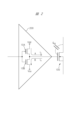
- FIG. 2 is a diagram showing an example of a circuit configuration using a silicon carbide power semiconductor device. It is a figure explaining the room for improvement which the present inventor paid attention to.
- FIG. 3 is a diagram illustrating the basic idea of suppressing the temperature dependence of "turn-on time.”
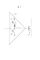
- FIG. 3 is a diagram illustrating the basic idea of suppressing the temperature dependence of "turn-off time.”
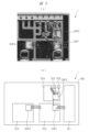
- (a) is a photograph showing an actual layout of a silicon carbide power semiconductor device
- (b) is a diagram schematically showing a layout of a silicon carbide power semiconductor device.
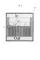
- FIG. 2 is a diagram showing the layout of a semiconductor chip in which CMOS transistors forming a switching control section are formed.
- FIG. 7 is an enlarged view showing a partial area of FIG.
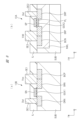
- FIG. 7 is a diagram showing a device structure in Modification 1.
- FIG. 7 is a diagram showing a device structure in Modification 2.
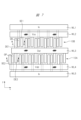
- FIG. 7 is a diagram showing a device structure in embodiment mode 2;
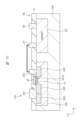
- FIG. 7 is a diagram showing a layout of a semiconductor chip in embodiment mode 3;
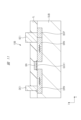
- 14 is a diagram collectively showing cross-sectional views taken along lines AA, line BB, and line CC in FIG. 13.
- Power semiconductor devices are required to have, for example, low on-resistance and low switching loss in addition to high breakdown voltage.
- the current mainstream power semiconductor device is a field effect transistor formed on a semiconductor substrate mainly composed of silicon, but this power semiconductor device is approaching its theoretical performance limit.
- a semiconductor device (hereinafter referred to as a wide band gap power semiconductor device) that includes a field effect transistor formed on a semiconductor substrate whose main component is a semiconductor material with a larger band gap than silicon is attracting attention.
- the breakdown voltage can be maintained even if the drift layer that maintains the breakdown voltage is thinned. For example, by making the drift layer thinner and increasing the impurity concentration, , the on-resistance of the power semiconductor device can be reduced.
- wide bandgap power semiconductor devices are excellent in that they can both improve breakdown voltage and reduce on-resistance, which are in a trade-off relationship with each other.
- a wide bandgap power semiconductor device having such advantages also has the advantage of being capable of high-temperature operation and high-speed switching operation due to the large bandgap.
- the technical idea in this embodiment is a technical idea regarding a wide bandgap power semiconductor device using a semiconductor material with a larger bandgap than silicon.
- semiconductor materials having a larger band gap than silicon include compound semiconductors represented by silicon carbide (SiC) and gallium nitride (GaN).
- SiC silicon carbide
- GaN gallium nitride
- the technical idea in this embodiment is not limited to these, and can be widely applied to wide bandgap power semiconductor devices using semiconductor materials with a larger bandgap than silicon.
- Silicon carbide has a dielectric breakdown field strength that is about one order of magnitude higher than that of silicon, so in order to ensure voltage resistance, the drift layer is made about 1/10th thinner and the impurity concentration is about 100 times higher. , the on-resistance (device resistance) can be theoretically reduced by three orders of magnitude or more.
- silicon carbide power semiconductor devices since the bandgap is about three times larger than that of silicon, high-temperature operation is possible, and wide bandgap power semiconductor devices using silicon carbide (hereinafter referred to as silicon carbide power semiconductor devices) are silicon carbide power semiconductor devices. It is expected that performance exceeding that of
- FIG. 1 is a diagram showing an example of a circuit configuration using a silicon carbide power semiconductor device 1.
- silicon carbide power semiconductor device 1 includes a power transistor 100, a Schottky barrier diode 110, and a switching control section 200.
- the power transistor 100 include a power MOSFET (Metal Oxide Semiconductor Field Effect Transistor) and an IGBT (Insulated Gate Bipolar Transistor). Note that power transistor 100, Schottky barrier diode 110, and switching control section 200 are formed using silicon carbide. Silicon carbide power semiconductor device 1 is connected to load 120 and external power supply 130 .
- an external power supply 130 is connected between a power supply potential Vd and a reference potential Vs, and a power transistor 100 and a Schottky barrier diode 110 are connected in series with the external power supply 130.
- a load 120 is connected in parallel to the Schottky barrier diode 110. This load 120 is, for example, a motor and includes an inductance.
- a switching control section 200 is connected to the gate of the power transistor 100, and the switching of the power transistor is controlled by this switching control section 200.
- the switching control section 200 includes a CMOS transistor, which is composed of a p-channel field effect transistor 10A and an n-channel field effect transistor 10B connected in series between a power supply potential Vdd and a reference potential Vss. has been done.
- a p-channel field effect transistor will be abbreviated as pFET
- nFET n-channel field effect transistor
- the inputs of the switching control section 200 are the gate of the pFET 10A and the gate of the nFET 10B, which are electrically connected to each other.
- the output of the switching control section 200 is a connection node between the drain of the pFET 10A and the drain of the nFET 10B, and this connection node is electrically connected to the gate of the power transistor 100.
- the switching of the power transistor 100 is controlled based on the control signal input to the input of the switching control section 200, and thereby the current flowing through the load 120 is controlled.
- Vss a low level signal
- Vss a low level signal
- Vdd a high level signal
- FIG. 1 it is assumed that a high level signal (for example, Vdd) is input to the input of the switching control section 200.
- Vdd a high level signal
- Vdd is applied to the gate of the pFET 10A forming the switching control section 200 and the gate of the nFET 10B forming the switching control section 200.
- pFET 10A is turned off, while nFET 10B is turned on. Therefore, a low level signal (for example, Vss) is output from the output of the switching control section 200.
- the switching operation of the power transistor 100 is controlled by the switching control section 200, so that the load 120 can be driven.
- FIG. 2 is a diagram illustrating the room for improvement that the inventor has focused on.
- t sw Switching time
- Q gd Amount of charge accumulated in the gate-drain capacitance of the power transistor I g : Gate current
- the gate current I g flows through the path "A" of the pFET10A is equivalent to the drain current of
- the gate current Ig is equivalent to the drain current of the nFET 10B flowing along the path "B".
- switching time is a concept that includes both “turn-on time” in which a power transistor transitions from an off state to an on state, and “turn-off time” in which a power transistor transitions from an on state to an off state. use.
- Turn-on time means that when the drain-source voltage (V ds ) when the power transistor is off is 100%, it changes from 90% of the drain-source voltage to 10% of the drain-source voltage. is defined as the time required for For example, when the drain-source voltage (V ds ) during off-state is 600V, the time for transition from 540V to 60V is defined as the "turn-on time”.
- Turn-off time is defined as 100% of the drain-source voltage (Vds) when the power transistor is off, because it changes from 10% of the drain-source voltage to 90% of the drain-source voltage. defined as the time required. For example, when the drain-source voltage (Vds) when turned off is 600V, the time for transition from 60V to 540V is defined as the "turn-off time”.
- the drain current during conduction changes as the temperature changes.
- the fact that the drain current of pFET 10A or nFET 10B (gate current I g of power transistor 100) changes with temperature change means that the power transistor This means that the switching time t sw of 100 is changed.
- the switching time t sw of the power transistor 100 is constant even if the temperature changes. From this, it can be seen that there is room for improvement in the circuit configuration of the switching control section 200 shown in FIG. 2 from the viewpoint of keeping the switching time tsw of the power transistor 100 constant even when the temperature changes.
- the basic idea of this embodiment is, for example, to compensate for the temperature dependence of the drain current of a CMOS transistor constituting the switching control section with the temperature dependence of a resistance component included in the switching control section.
- the basic idea is to provide a resistance component in the switching control section that has characteristics opposite to the temperature dependence of the gate current of the power transistor whose switching is controlled by the switching control section, so that changes in the gate current due to temperature changes are caused by changes in the gate current due to temperature changes. This can also be said to be an idea that is suppressed by the change in the resistance component described above.
- FIG. 3 is a diagram illustrating the basic idea of suppressing the temperature dependence of "turn-on time”.
- the drain current flowing through the pFET 10A corresponds to the gate current flowing into the gate of the power transistor 100. Since the drain current flowing through the pFET 10A changes as the temperature changes, the gate current changes as the temperature changes.
- the drain current flowing through the pFET 10A is treated as increasing as the temperature rises.
- the gate current flowing into the gate of power transistor 100 increases as the temperature rises.
- the basic idea in FIG. 3 is to provide the resistance component 20 included in the switching control section 200 between the drain of the pFET 10A constituting the switching control section 200 and the gate of the power transistor 100.
- this resistance component 20 is composed of a resistance component having characteristics opposite to the temperature dependence of the drain current of the pFET 10A.
- a change in the drain current of the pFET 10A is suppressed by a change in the resistance component 20.
- the resistance component 20 is composed of a resistance component that has a characteristic that its resistance value increases as the temperature rises.
- an increase in the drain current of the pFET 10A is suppressed by an increase in the resistance value of the resistance component 20.
- I g (V dd - V g (T))/(Rpf (T) + Rpw (T)) ...
- I g Gate current
- V dd Power supply potential of switching control section
- V g (T): Gate voltage ( Miller plateau voltage)
- T Temperature
- Equation 2 is an expression expressing the gate current Ig of the power transistor 100 during the "turn-on time", and this gate current Ig can also be said to be the drain current of the pFET 10A.
- V g (T) is the Miller plateau voltage, whose value decreases with increasing temperature.
- the Miller plateau voltage V g (T) is the gate voltage value at which charging and discharging of the Miller capacitance begins during switching.
- the Miller plateau voltage V g (T) decreases as the temperature increases, mainly due to a decrease in the threshold voltage of the power transistor 100 as the temperature increases.
- Rpf(T) means the equivalent resistance excluding the wiring resistance of the pFET 10A, and is typically the channel resistance, and the resistance value decreases as the temperature rises. In other words, this shows the characteristic that the drain current of the pFET 10A increases as the temperature rises.
- Rpw(T) is typically the wiring resistance of the pFET 10A, but may also be a resistance connected to the drain end and/or source end of the pFET 10A. Rpw(T) corresponds to the resistance component 20 in FIG.
- the basic idea regarding the "turn-on time” is that the temperature dependence of the resistance component Rpw(T) (resistance component 20) of the switching control section 200 is a temperature dependence in which the resistance value increases as the temperature rises.
- the idea is that the change in the gate current Ig of the power transistor 100 due to temperature rise can be reduced.
- (Equation 1) changes in "turn-on time” due to temperature changes can be reduced.
- FIG. 3 describes an example in which the resistance component 20 is provided on the drain side of the pFET 10A
- the basic idea regarding the "turn-on time" is not limited to this.
- the resistance component 20 may be provided on the source side of the pFET 10A.
- the resistance component 20 may be provided on both the drain side and the source side.
- FIG. 4 is a diagram illustrating the basic idea of suppressing the temperature dependence of "turn-off time”.
- the drain current flowing through the nFET 10B corresponds to the gate current flowing out from the gate of the power transistor 100. Since the drain current flowing through the nFET 10B changes as the temperature changes, the gate current changes as the temperature changes. In particular, the drain current flowing through the nFET 10B is treated as increasing as the temperature rises. In this case, the gate current of power transistor 100 increases as the temperature rises.
- the basic idea in FIG. 4 is to provide the resistance component 30 included in the switching control section 200 between the drain of the nFET 10B constituting the switching control section 200 and the gate of the power transistor 100.
- this resistance component 30 is composed of a resistance component having characteristics opposite to the temperature dependence of the drain current of the nFET 10B.
- a change in the drain current of the nFET 10B is suppressed by a change in the resistance component 30.
- the resistance component 30 is composed of a resistance component that has a characteristic that its resistance value increases as the temperature rises.
- an increase in the drain current of the nFET 10B is suppressed by an increase in the resistance value of the resistance component 30.
- I g (V g (T) - V ss )/(Rnf (T) + Rnw (T)) ... (Formula 3)
- I g Gate current
- V ss Reference potential of switching control section
- Rnf(T) Equivalent resistance excluding wiring resistance of nFET10A
- Rnw(T) Resistance component (wiring resistance)
- T Temperature V g (T) is the Miller plateau voltage, and its value decreases as the temperature increases.
- Rnf(T) means the equivalent resistance excluding the wiring resistance of nFET 10B, and is typically the channel resistance, and the resistance value decreases as the temperature increases. In other words, this represents a characteristic in which the drain current of the nFET 10B increases as the temperature rises.
- Rnw(T) is typically the wiring resistance of the nFET 10B, but may also be a resistance connected to the drain end and/or the source end of the nFET 10B. Rnw(T) corresponds to the resistance component 30 in FIG.
- Equation 1 Q gd hardly changes with temperature, so if the fluctuation of gate current I g with respect to temperature change can be suppressed, the temperature fluctuation of "turn-off time" can be suppressed.
- Equation 3 Rnf(T) increases Ig when its value decreases, and Rnw(T) decreases Ig when its value increases.
- V g (T) increases, I g increases, which is an inverse relationship to (Formula 2).
- T increases, Rnf(T) decreases and Ig increases, but Vg (T) decreases, causing Ig to decrease, and both have opposite effects on Ig . Therefore, the following three cases are possible.
- the basic idea regarding the "turn-off time" is that the temperature dependence of the drain current flowing through the nFET 10B has a greater influence than the temperature dependence of the gate voltage Vg of the power transistor 100, and It is necessary to separate the cases in which the temperature dependence of the gate voltage V g has a greater influence than the temperature dependence of the drain current flowing through the nFET 10B.
- the basic idea regarding the "turn-off time” is that the resistance of the switching control section 200 It is said that if the temperature dependence of the component Rnw(T) (resistance component 30) is such that the resistance value increases as the temperature rises, it is possible to reduce the change in the gate current Ig due to the rise in temperature. It is a thought. In this case, based on (Equation 1), changes in "turn-off time" due to temperature changes can be reduced.
- the basic idea regarding the "turn-off time” is that the resistance of the switching control section 200 It is said that if the temperature dependence of the component Rnw(T) (resistance component 30) is such that the resistance value decreases as the temperature rises, it is possible to reduce the change in the gate current Ig due to the rise in temperature. It is a thought. In this case, based on (Equation 1), changes in "turn-off time" due to temperature changes can be reduced.
- FIG. 4 describes an example in which the resistance component 30 is provided on the drain side of the nFET 10B, the basic idea regarding the "turn-off time" is not limited to this.
- the resistance component 30 may be provided on the source side of the nFET 10B.
- the resistance component 30 may be provided on both the drain side and the source side.
- FIG. 5 is a diagram showing the layout of silicon carbide power semiconductor device 1. As shown in FIG. In particular, Fig. 5(a) is a photograph showing an actual layout example of silicon carbide power semiconductor device 1, and FIG. 5(b) is a diagram schematically showing the layout of silicon carbide power semiconductor device 1.
- silicon carbide power semiconductor device 1 has wiring board WB. Terminals TE1 to TE6, which serve as conductor regions, are formed on this wiring board WB.
- the wiring board WB is made of, for example, a SiN-AMC (silicon nitride-active metal copper circuit) board and a Cu bonded to the bottom surface of the SiN-AMC (silicon nitride-active metal copper circuit) board in order to improve heat dissipation and match the coefficient of thermal expansion with the semiconductor chip.
- a base substrate made of a Mo-Cu (CMC) composite material.
- terminal TE6 When looking at the silicon carbide power semiconductor device 1 as a whole, terminal TE6 becomes a signal input node (IN in FIG. 1), and terminal TE2 becomes an output node (drain of the power transistor).
- the other terminals TE1, TE3 to TE5 serve as power supply nodes.
- a reference potential Vs shown in FIG. 1 is applied to the terminal TE1, and a power supply potential Vd shown in FIG. 1 is applied to the terminal TE3. Further, the reference potential Vss shown in FIG. 1 is applied to the terminal TE4, and the power supply potential Vdd shown in FIG. 1 is applied to the terminal TE5.
- a semiconductor chip CHP1 on which a power transistor is formed is mounted on the terminal TE2, and a semiconductor chip CHP3 on which a Schottky barrier diode is formed is mounted on the terminal TE3. Moreover, a semiconductor chip CHP2 in which a CMOS transistor forming a switching control section is formed is mounted on the terminal TE4.
- the terminal TE1 is connected by a wire to the source of a power transistor formed in the semiconductor chip CHP1. Further, the terminal TE2 is connected by a wire to the anode of a Schottky barrier diode formed in the semiconductor chip CHP3.
- the terminal TE4 is connected by a wire to the source of an nFET that constitutes a CMOS transistor formed in the semiconductor chip CHP2. Further, the terminal TE5 is connected by a wire to the source of a pFET that constitutes a CMOS transistor. Further, the terminal TE6 is connected by a wire to the gates of the pFET and the nFET, which are electrically connected to each other. That is, the terminal TE6 is connected by a wire to the input of the CMOS transistor that constitutes the switching control section.
- the semiconductor chip CHP1 and the semiconductor chip CHP2 are connected by a wire. Specifically, the gate of the power transistor formed in the semiconductor chip CHP1 and the output of the CMOS transistor formed in the semiconductor chip CHP2 are connected by a wire.
- silicon carbide power semiconductor device 1 laid out in this manner, semiconductor chip CHP1 and semiconductor chip CHP2 are arranged closely. This means that the output of the CMOS transistor formed in the semiconductor chip CHP2 and the gate of the power transistor formed in the semiconductor chip CHP1 are connected by a short wire. As a result, the parasitic inductance of the wire can be reduced, allowing high-speed switching operation. For example, in silicon carbide power semiconductor device 1 having the layout shown in FIG. 5, a switching time of several ns can be realized. In other words, it is possible to realize a "turn-on time” and a "turn-off time" of several ns or less.
- a power transistor chip semiconductor chip CHP1
- a CMOS transistor chip semiconductor c-hip CHP2
- the heat generated by the power transistor chip is linked to the temperature of the CMOS transistor chip.
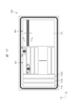
- FIG. 6 is a diagram showing the layout of the semiconductor chip CHP2 in which the CMOS transistors constituting the switching control section are formed.
- a plurality of pads are formed on the surface of the semiconductor chip CHP2. Specifically, in the semiconductor chip CHP2, an input pad (In) of a CMOS transistor, a power supply potential pad (Vdd), a reference potential pad (Vss), and an output pad (Out) of a CMOS transistor are formed.
- FIG. 7 is an enlarged view showing area RA in FIG. 6.
- metal wires WL1 to WL5 are arranged in the y direction, and each of the metal wires WL1 to WL5 extends in the x direction.
- Each of these metal wires WL1 to WL5 is composed of, for example, an aluminum wire containing aluminum as a main component.
- main component refers to the component that is present in the largest amount, and is used to indicate that other components may also be included.
- containing aluminum as a main component means containing the largest amount of aluminum.
- the metal wiring WL1 is an input wiring (In) of the CMOS transistor, and the metal wiring WL2 is a reference wiring to which a reference potential (Vss) is applied. Further, the metal wiring WL3 is an output wiring (Out) of the CMOS transistor, and the metal wiring WL4 is a power wiring to which a power supply potential (Vdd) is applied. Further, the metal wiring WL5 is an input wiring (In) of the CMOS transistor. In the metal wirings WL1 to WL5 configured in this way, a plurality of nFETs 10B constituting a CMOS transistor are formed between the metal wiring WL2 and the metal wiring WL3, and the plurality of nFETs 10B are lined up in the x direction.
- Each of the plurality of nFETs 10B has a source electrode SE1 and a drain electrode DE1, and also has a gate electrode GN disposed between the source electrode SE1 and the drain electrode DE1.
- the source electrode SE1 is electrically connected to the metal wiring WL2, while the drain electrode DE1 is electrically connected to the metal wiring WL3. Further, the gate electrode GN is electrically connected to the metal wiring WL1.
- a plurality of pFETs 10A forming a CMOS transistor are formed between the metal wiring WL3 and the metal wiring WL4, and the plurality of pFETs 10A are arranged in line in the x direction.
- Each of these pFETs 10A has a source electrode SE2 and a drain electrode DE2, and also has a gate electrode GP disposed between the source electrode SE2 and the drain electrode DE2.
- the source electrode SE2 is electrically connected to the metal wiring WL4, while the drain electrode DE2 is electrically connected to the metal wiring WL3.
- the gate electrode GP is electrically connected to the metal wiring WL5.
- the source electrode SE1 and the source electrode SE2, the drain electrode DE1 and the drain electrode DE2, the metal wiring WL2, the metal wiring WL3, and the metal wiring WL4 are formed of aluminum wiring in the same layer, and are patterned by photolithography.
- the layout of the semiconductor chip CHP2 is configured.
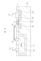
- FIG. 8(a) is a cross-sectional view taken along the line AA in FIG. 7, and is a diagram showing the device structure of the nFET 10B that constitutes a CMOS transistor.
- a drain region DRN made of an n-type diffusion layer and a source region SRN made of an n-type diffusion layer are formed spaced apart in a p-type silicon carbide substrate SUB.
- a p-type body contact region BCP is formed in contact with the source region SRN.
- a region sandwiched between the source region SRN and the drain region DRN is a channel formation region, and a gate insulating film GOX1 is formed on this channel formation region. Then, a gate electrode GN is formed on the gate insulating film GOX1.
- an insulating layer IL is formed on the surface of the p-type silicon carbide substrate SUB covering the gate electrode GN, and a drain electrode DE1 and a source electrode SE1 are formed so as to penetrate this insulating layer IL.
- the drain electrode DE1 is formed to penetrate the insulating layer IL and reach the drain region DRN, and is electrically connected to the drain region DRN.
- the source electrode SE1 is formed to penetrate the insulating layer IL to reach both the source region SRN and the p-type body contact region BCP, and is electrically connected to the source region SRN and the p-type body contact region BCP. has been done.
- the drain electrode DE1 is electrically connected to the metal wiring WL3 in a planar direction (not shown) (see FIG. 7).
- the source electrode SE1 is electrically connected to the metal wiring WL2 in a planar direction (not shown) (see FIG. 7).
- nFET 10B is configured.
- FIG. 8(b) is a cross-sectional view taken along the line BB in FIG. 7, and is a diagram showing the device structure of the pFET 10A that constitutes a CMOS transistor.
- an n-type well NWL is formed in a p-type silicon carbide substrate SUB, and within this n-type well NWL, a drain region DRP made of a p-type diffusion layer and a p-type diffusion layer made of a p-type diffusion layer are formed. Source regions SRP are formed apart from each other. Then, an n-type body contact region BCN is formed so as to be in contact with the source region SRP. On the other hand, a depleted p-type buried region PL is formed in a region sandwiched between the source region SRP and the drain region DRP, and a gate insulating film GOX2 is formed on this p-type buried region PL. Then, a gate electrode GP is formed on the gate insulating film GOX2.
- an insulating layer IL is formed on the surface of the p-type silicon carbide substrate SUB that covers the gate electrode GP, and a drain electrode DE2 and a source electrode SE2 are formed so as to penetrate this insulating layer IL.
- the drain electrode DE2 is formed to penetrate the insulating layer IL and reach the drain region DRP, and is electrically connected to the drain region DRP.
- the source electrode SE2 is formed to penetrate through the insulating layer IL to reach both the source region SRP and the n-type body contact region BCN, and is electrically connected to the source region SRP and the n-type body contact region BCN. has been done.
- the drain electrode DE2 is electrically connected to the metal wiring WL3 in a planar direction (not shown) (see FIG. 7).
- the source electrode SE2 is electrically connected to the metal wiring WL4 in a planar direction (not shown) (see FIG. 7).
- pFET10A is configured.
- the pFET 10A a depleted p-type buried region PL is formed in the channel formation region.
- the pFET 10A employs a so-called "buried channel structure" in which a channel is formed below the p-type buried region PL. The reason for this is as follows.
- a field effect transistor formed on a silicon carbide substrate has a high density of interface states at the MOS interface, resulting in decreased channel mobility and increased on-resistance.
- This interface state occurs, for example, in a heat treatment step when forming a gate insulating film, and becomes particularly noticeable when the threshold voltage of the pFET increases.
- a donor-like trap exists near the center of the band gap, and once a hole is trapped, thermal energy is lost due to the large band gap of silicon carbide. Then you won't be able to detrap.
- the trapped holes behave as effective positive fixed charges, thereby shifting the threshold voltage of pFET 10A negatively. In other words, the threshold voltage of pFET 10A increases.
- this hole trap also exists in the nFET 10B, and when a negative gate bias is applied, an effective positive fixed charge is generated.
- a "buried channel structure” is adopted instead of a “surface channel structure” so as not to be affected by the interface state.
- the "buried channel structure” is formed of an epitaxial layer. Thereby, since impurities are not implanted by ion implantation, the on-resistance of the pFET 10A can be reduced, and the threshold voltage can be reduced.
- FIG. 8 shows a structure in which pFET 10A and nFET 10B are formed on a p-type silicon carbide substrate SUB
- a p-type silicon carbide substrate SUB if it is difficult to use a p-type silicon carbide substrate SUB, an n-type silicon carbide substrate or a semi-insulating silicon carbide substrate may be used.
- a similar structure can be formed by epitaxially growing a p-type silicon carbide layer thereon.
- the structure of the CMOS area AR1 which will be described later in FIG. 14, can also be used as is.
- the feature of embodiment 1 is that, for example, as shown in FIG. 7, metal wirings WL2 to WL4 are used as resistance components electrically connected to the CMOS transistors.
- the feature of embodiment 1 is that the wiring resistance of the metal wirings WL2 to WL4 is used as the above-mentioned resistance component by intentionally extending the metal wirings WL2 to WL4 in the x direction. .
- the change in the "turn-on time” as the temperature rises means that the temperature dependence of the resistance component Rpw(T) of the switching control section changes as the resistance value increases as the temperature rises. can be made smaller if it has an increasing temperature dependence.
- a temperature-dependent resistance component whose resistance value increases as the temperature rises as the resistance component electrically connected to the pFET 10A, changes in the "turn-on time" can be suppressed.
- the resistance component electrically connected to the pFET 10A is the wiring resistance of the metal wiring WL3 electrically connected to the drain electrode DE2 of the pFET 10A.
- a metal wiring WL4 electrically connected to the source electrode SE2 of the pFET 10A is used.
- the metal wiring WL3 and the metal wiring WL4 are formed of wiring whose main component is aluminum, and have a characteristic that the resistance value increases as the temperature rises. Therefore, according to embodiment 1, the change in the "turn-on time" is suppressed by the change in the wiring resistance of the metal wiring WL3 and the change in the wiring resistance of the metal wiring WL4. It can be held almost constant.
- the temperature dependence of the drain current flowing through the nFET 10B has a greater influence than the temperature dependence of the gate voltage V g of the power transistor 100, and the case where the temperature dependence of the gate voltage V g of the power transistor 100 has a larger effect than the temperature dependence of the gate voltage V g of the power transistor 100. It is necessary to separate the case where the influence is greater than the temperature dependence of the drain current flowing through the nFET 10B.
- the temperature dependence of the resistance component Rnw(T) of the switching control section If the resistance is temperature dependent, in which the resistance value increases as the temperature rises, changes in the "turn-off time" can be reduced. In particular, by using a resistance component that has the characteristic of increasing its resistance value as the temperature rises as the resistance component electrically connected to the nFET 10B, changes in the "turn-off time" can be suppressed.
- the resistance component electrically connected to the nFET 10B is the wiring resistance of the metal wiring WL3 electrically connected to the drain electrode DE1 of the nFET 10B.
- a metal wiring WL2 electrically connected to the source electrode SE1 of the nFET 10B is used.
- the metal wiring WL2 and the metal wiring WL3 are formed of wiring whose main component is aluminum, and have a characteristic that the resistance value increases as the temperature rises. Therefore, according to embodiment 1, under conditions where the temperature dependence of the drain current flowing through the nFET 10B has a greater influence than the temperature dependence of the gate voltage Vg of the power transistor 100, the "turn-off time" changes. is suppressed by the change in the wiring resistance of the metal wiring WL2 and the wiring resistance of the metal wiring WL3, and as a result, the "turn-off time" can be held substantially constant regardless of temperature rise.
- FIG. 9 is a graph showing the temperature dependence of "turn-on time”.
- the horizontal axis is temperature (° C.)
- the vertical axis is “turn-on time” (ns).
- the plots of black circles are experimental data, while the plots of white circles are calculated data.
- the "turn-on time” near room temperature (25° C.) is 8.5 ns, and once the temperature rises to around 200° C., the “turn-on time” once decreases to 7 ns. Thereafter, when the temperature rises from around 200°C to around 300°C, the “turn-on time” increases.
- Such behavior can be qualitatively explained, for example, as follows. That is, first, below 200° C., as the temperature rises, the gate voltage (Miller plateau voltage) decreases and the drain current of the pFET 10A increases.
- the decrease in the "turn-on time" of the power transistor 100 due to temperature change is caused by the resistance components electrically connected to the CMOS transistor (the wiring resistance of the metal wiring WL3 and the wiring resistance of the metal wiring WL4). This proves that this is suppressed by an increase in the resistance value of the resistance (resistance) due to temperature changes.
- the "turn-off time” hardly changes even if the temperature changes in a high-speed switching operation where the switching time is several ns. This is because the switching time is faster than the charging time for accumulating charge in the output capacitance of the power transistor 100 and the Schottky barrier diode 110, so the "turn-off time” is determined by the charging time. That is, for example, as shown in FIG. 5, in silicon carbide power semiconductor device 1 in embodiment mode 1, semiconductor chip CHP1 on which power transistor 100 is formed and semiconductor chip CHP2 on which CMOS transistor is formed are arranged close to each other. As a result, high-speed switching operation (several ns) is possible.
- the basic idea is that the change in the "turn-off time” is suppressed by the change in the wiring resistance of the metal wiring WL2 and the change in the wiring resistance of the metal wiring WL3. I can say that you don't have to.
- high-speed switching operation is defined as a switching operation in which the switching time is several ns (for example, 9 ns or less) or less.
- the switching time may be 7 ns or more and 8 ns or less.
- low-speed switching operation can be defined as a switching operation with a slower switching time than "high-speed switching operation.”
- a switching operation in which the switching time is on the order of tens of ns (for example, 10 ns or more and 99 ns or less) can be mentioned.
- the "turn-off time” is also slower than the discharge time of the charge amount, so it is considered that the turn-off time is not rate-limited by the discharge time and has temperature dependence.
- the resistance components electrically connected to the nFET 10B include the wiring resistance of the metal wiring WL3 that is electrically connected to the drain electrode DE1 of the nFET 10B, and the metal wiring WL2 that is electrically connected to the source electrode SE1 of the nFET 10B.
- the configuration of Embodiment 1 using the above is useful in that the "turn-off time" can be kept substantially constant regardless of temperature rise.
- FIG. 10 is a diagram showing a device structure in Modification 1.
- p-type silicon carbide substrate SUB is provided with pFET 10A and n-type resistance element RD.
- n-type resistance element RD includes an n-type semiconductor region RN formed in p-type silicon carbide substrate SUB, and a pair of electrodes EA and EB electrically connected to this n-type semiconductor region RN. are doing.
- the drain electrode DE2 of the pFET 10A and the electrode EA of the n-type resistance element RD are electrically connected by wiring.
- the resistance of the n-type semiconductor region RN forming the n-type resistance element RD is used as the resistance component electrically connected to the pFET 10A.
- the n-type semiconductor region RN has a characteristic that the resistance value increases as the temperature rises.
- the "turn-on time" of the power transistor 100 decreases with the temperature rise due to an increase in the resistance value with the temperature rise of the n-type semiconductor region RN constituting the n-type resistance element RD. can be suppressed.
- n-type resistance element RD was provided so as to be electrically connected to the drain electrode DE2 of the pFET 10A.
- the configuration in Modification 1 is not limited to this, and an n-type resistance element RD may be provided so as to be electrically connected to the source electrode SE2 of the pFET 10A.
- an n-type resistance element RD electrically connected to the drain electrode DE2 and an n-type resistance element RD electrically connected to the source electrode SE2 may be provided.
- the resistance of the n-type semiconductor region RN constituting the n-type resistance element RD can also be used as a resistance component electrically connected to the nFET 10B.
- the nFET 10B if the condition is satisfied that the temperature dependence of the drain current flowing through the nFET 10B has a greater influence than the temperature dependence of the gate voltage Vg of the power transistor 100, then the n The increase in the resistance value as the temperature of the type semiconductor region RN increases, suppresses a decrease in the "turn-off time" of the power transistor 100 as the temperature increases.
- nFET 10B is electrically connected to the The idea is to use a resistance component whose resistance value increases as the temperature rises.
- the n-type resistance element RD can be used as the resistance component electrically connected to the nFET 10B.
- the source region SRN and drain region DRN are composed of n-type semiconductor regions. Therefore, by adjusting the sizes of the source region SRN and the drain region DRN to have a resistance component, it is possible to create a resistance component that is electrically connected to the nFET 10B by adjusting the size of the source region SRN and the drain region DRN.
- the basic idea of using a component (n-type semiconductor region) can be realized.
- FIG. 11 is a diagram showing a device structure in Modification 2.
- the size of the source region SRN is increased and the size of the drain region DRN is increased.
- the width of the source region SRN in the x direction and the width of the drain region DRN in the x direction are increased.
- the parasitic resistance components of the source region SRN and drain region DRN which are n-type semiconductor regions, can be adjusted. Therefore, according to the present modification example 2, it is possible to provide the source region SRN and the drain region DRN with a resistance component made of an n-type semiconductor region, and thereby the resistance value increases as the temperature rises. It is possible to provide a resistance component having a value of . As a result, it is possible to suppress a decrease in the "turn-off time" of the power transistor 100 due to a rise in temperature.
- the resistance component electrically connected to the nFET 10B By using a resistance component whose resistance value decreases as the temperature rises, it is possible to suppress an increase in the "turn-off time" of the power transistor 100 as the temperature rises (basic idea).
- FIG. 12 is a diagram showing a device structure in implementation mode 2.
- a p-type resistance element RD2 is provided on a p-type silicon carbide substrate SUB along with an nFET 10B.
- p-type resistance element RD2 is connected to p-type semiconductor region RP included in n-type well NWL formed in p-type silicon carbide substrate SUB, and a pair of p-type semiconductor regions RP electrically connected to this p-type semiconductor region RP. It has an electrode EA2 and an electrode EB2. Then, the drain electrode DE1 of the nFET 10B and the electrode EA2 of the p-type resistance element RD2 are electrically connected by wiring.
- the resistance of the p-type semiconductor region RP constituting the p-type resistance element RD2 is used as the resistance component electrically connected to the nFET 10B.
- p-type semiconductor region RP has a characteristic that the resistance value decreases as the temperature rises.
- Al aluminum
- N nitrogen
- P phosphorus
- the "turn-on time" of the power transistor 100 increases as the temperature rises due to a decrease in the resistance value as the temperature rises in the p-type semiconductor region RP constituting the p-type resistance element RD2. can be suppressed.
- the p-type resistance element RD2 is provided so as to be electrically connected to the drain electrode DE1 of the nFET 10B.
- the configuration in embodiment mode 2 is not limited to this, and a p-type resistance element RD2 may be provided so as to be electrically connected to the source electrode SE1 of the nFET 10B.
- a p-type resistance element RD2 electrically connected to the drain electrode DE1 and a p-type resistance element RD2 electrically connected to the source electrode SE1 may be provided.
- Embodiment mode 3 an example will be described in which the basic idea of the embodiment is applied to a semiconductor device in which a power transistor 100 and a switching control section 200 (CMOS transistor) are formed in one semiconductor chip.
- CMOS transistor switching control section 200
- FIG. 13 is a diagram showing the layout of the semiconductor chip CHP in embodiment mode 3.
- the semiconductor chip CHP includes an input signal terminal TVin, a CMOS reference potential terminal TVSS, a CMOS power supply potential terminal TVDD, a power source terminal TVs, a CMOS region AR1 (switching control section region), and a power transistor region BR1.
- a CMOS area AR1 is arranged in the center of the semiconductor chip CHP, and on one side (left side) of the CMOS area AR1 is an input signal terminal TVin, a CMOS reference potential terminal TVSS, and a CMOS power supply potential terminal TVDD. is located.
- a power transistor region BR1 is arranged on the other side (right side) of the CMOS region AR1. Note that the power source terminal TVs is located within the power transistor region BR1 and above the power transistor.
- FIG. 14 is a diagram collectively showing cross-sectional views taken along the lines AA, BB, and C-C in FIG. 13, and shows the device structure of the unit transistor in each region.
- the region NAR is a region where the nFET 10B constituting the switching control section (CMOS transistor) is formed, and corresponds to the AA cross-sectional view.
- the region PAR is a region where the pFET 10A constituting the switching control section (CMOS transistor) is formed, and corresponds to the BB cross-sectional view.
- a region BR1 is a region where the power transistor 100 is formed, and corresponds to the CC cross-sectional view.
- the semiconductor chip CHP includes a power transistor region BR1 and a CMOS region AR1.
- a power transistor 100 is formed in the power transistor region BR1, while an nFET 10B is formed in a region NAR of the CMOS region AR1.
- a pFET 10A is formed in the region PAR of the CMOS region AR1.
- the power transistor 100 is composed of a trench gate type power MOSFET having a gate, a source, and a drain.
- the nFET 10B is composed of a surface channel type MOSFET having a gate, a source, and a drain
- the pFET 10A is composed of a buried channel type MOSFET having a gate, source, and drain.
- the power transistor 100, nFET 10B, and pFET 10A are formed on a laminated semiconductor substrate SB.
- the laminated semiconductor substrate SB includes a drift layer (n-type semiconductor layer) DL formed on the semiconductor substrate SUB1, a buried base layer (p-type semiconductor layer) BBL formed on the drift layer DL, and a layer on the buried base layer BBL.
- the base layer (p-type semiconductor layer) BL is formed in the following manner.
- Semiconductor substrate SUB1 is an n-type silicon carbide substrate, and its polytype is, for example, 4H. In other words, the semiconductor substrate SUB1 is composed of an n-type 4H-SiC substrate.
- the drift layer DL is an n-type semiconductor layer, and is composed of an epitaxial layer formed on the semiconductor substrate SUB1 using an epitaxial growth method.
- the buried base layer BBL is a p-type semiconductor layer formed on the drift layer DL using an epitaxial growth method and an ion implantation method.
- the thickness of the buried base layer BBL is approximately 1 ⁇ m.
- the buried base layer BBL has a laminated structure of a buried base layer BBL1 and a buried base layer BBL2, and the film thicknesses of the buried base layer BBL1 and the buried base layer BBL2 are each about 0.5 ⁇ m.
- the base layer BL is a p-type semiconductor layer, and is, for example, an epitaxial layer formed on the buried base layer BBL using an epitaxial growth method.
- the thickness of the base layer BL is thicker than the thickness of the buried base layer BBL.
- the p-type impurity concentration of the base layer BL is lower than the p-type impurity concentration of the buried base layer BBL.
- a channel formation region of the power transistor 100 is formed in the power transistor region BR1, while an nFET 10B and a pFET 10A are formed in the CMOS region AR1.
- the base layer BL By making the base layer BL an epitaxial layer formed by an epitaxial growth method, the base layer BL having a relatively thick film thickness can be formed without using a special ion implantation device capable of outputting MeV class ion implantation energy. be able to. Thereby, it is possible to improve the degree of freedom in voltage resistance design, etc. in the CMOS region AR1.
- the semiconductor substrate SUB1, the drift layer DL, and the base layer BL are provided throughout the power transistor region BR1 and the CMOS region AR1.
- the buried base layer BBL is provided throughout the CMOS region AR1, while it is selectively provided in the power transistor region BR1.
- a trench protection region (p-type semiconductor region) TPR is provided at the bottom of the trench trench TG, and a JFET layer (n-type semiconductor layer) DLS1 and a JFET layer (n-type semiconductor layer) are provided around the trench trench TG and trench protection region TPR. ) DLS2 is provided.
- the buried base layer BBL is arranged in a region other than the region where the trench protection region TPR, the JFET layer DLS1, and the JFET layer DLS2 are provided. Further, on the back surface of the semiconductor substrate SUB1, a drain electrode ED is formed over the entire area of the power transistor region BR1 and the CMOS region AR1.
- a trench groove TG is formed that penetrates the source region RSU and the base layer BL from the surface of the laminated semiconductor substrate SB, and a gate insulating film GIU and a gate electrode EGU are formed in the trench groove TG. ing.
- the gate insulating film GIU is, for example, a silicon oxide film formed using a CVD method.
- Gate electrode EGU is formed from a polysilicon film containing n-type impurities.
- a source region (n-type semiconductor region) RSU and a p-type region (p-type semiconductor region) RPU are formed in the base layer BL.
- the source regions RSU are arranged on both sides of the trench TG so as to sandwich the trench TG.
- the p-type region (p-type semiconductor region) RPU is arranged on the opposite side of the trench groove TG or the gate electrode EGU with respect to the source region RSU. In other words, it can be said that the p-type region RPU is arranged between the source regions RSU of adjacent unit transistors.
- the source region RSU and the p-type region RPU are electrically connected to the source electrode ESU.
- the p-type impurity concentration of the trench protection region (p-type semiconductor region) TPR provided at the bottom of the trench trench TG is equal to the p-type impurity concentration of the buried base layer BBL and higher than the p-type impurity concentration of the base layer BL.
- the trench protection region (p-type semiconductor region) TPR is an electric field relaxation layer.
- This trench protection region TPR has a structure in which the trench TG digs into the trench protection region TPR at the bottom of the trench TG in order to alleviate the concentration of electric field on the gate insulating film GIU at the bottom of the trench TG. has been done. That is, the depth of the trench groove TG is greater than the total thickness of the base layer BL and buried base layer BBL2, and smaller than the total thickness of the base layer BL and buried base layer BBL.
- the trench protection region TPR is sandwiched between the JFET layer (n-type semiconductor layer) DLS1, and the trench trench TG is sandwiched between the JFET layer (n-type semiconductor layer) DLS2. . Since the gate insulating film GIU is covered with the trench protection region TPR at the bottom of the trench trench TG, dielectric breakdown of the gate insulating film GIU can be prevented. Further, by optimizing the n-type impurity concentration of the JFET layer DLS1 and the JFET layer DLS2, dielectric breakdown of the gate insulating film GIU can be prevented without increasing the JFET resistance.
- the drain-source breakdown voltage of the power transistor 100 is can be improved.
- the base layer BL in which the channel of the power transistor 100 is formed with an epitaxial layer with a low impurity concentration high channel mobility can be ensured, and thereby the on-resistance of the power transistor 100 can be reduced. . That is, by providing the buried base layer BBL and the base layer BL having different p-type impurity concentrations, it is possible to improve the withstand voltage between the drain and source and reduce the on-resistance without being influenced by each other.
- the power transistor 100 is configured as described above.
- the nFET 10B includes a source region (n-type semiconductor region) RSN and a drain region (n-type semiconductor region) RDN formed in the base layer BL, and a channel region RCN provided between the source region RSN and the drain region RDN. , and a gate electrode EGN formed over the channel region RCN with a gate insulating film GIN interposed therebetween.
- the nFET 10B is a surface channel MOSFET, and when a desired gate voltage is applied to the gate electrode EGN, a channel is formed in the channel region RCN directly under the interface between the base layer BL and the gate insulating film GIN.
- the channel region RCN provided between the source region RSN and drain region RDN of the nFET 10B is a part of the p-type base layer BL, and impurity ions for adjusting the threshold voltage are not ion-implanted into the channel region RCN. Therefore, the p-type impurity concentration of the channel region RCN is equal to the p-type impurity concentration of the base layer BL.
- the pFET 10A is formed in an n-type well region (n-type semiconductor region) NW formed in the base layer BL.
- the pFET 10A is formed between a source region (p-type semiconductor region) RSP and a drain region (p-type semiconductor region) RDP formed in the n-type well region NW, and a gate insulating film GIP on the surface of the laminated semiconductor substrate SB. and a gate electrode EGP.
- the pFET 10A is a buried channel MOSFET and has a buried channel region EBC with a thickness of about 0.2 ⁇ m from the surface of the laminated semiconductor substrate SB.
- the buried channel region EBC is a p-type semiconductor region within the n-type well NW, but is a region in which n-type impurities are not substantially ion-implanted.
- a desired voltage is applied to the gate electrode EGP, a channel is formed not directly below the interface between the buried channel region EBC and the gate insulating film GIP, but at a position deeper than the interface.
- the n-type well region NW is composed of an n-type well layer (n-type semiconductor layer) NW1, an n-type well layer (n-type semiconductor layer) NW2, and an n-type well layer (n-type semiconductor layer) NW3.
- the n-type well layer NW1 is provided at a relatively deep position from the surface of the laminated semiconductor substrate SB, and the n-type well layer 2NW2 is provided on the n-type well layer NW1.
- the n-type well layer NW1 and the n-type well layer NW2 are formed, for example, by implanting nitrogen ions into the base layer BL.
- the p-type impurity concentration of the buried channel region EBC is equal to the p-type impurity concentration of the base layer BL.
- the p-type impurity concentration of the base layer BL means, for example, the p-type impurity concentration in the channel formation region of the power transistor 100.
- a CMOS transistor is configured as described above.
- metal wiring can be used as a resistance component electrically connected to a CMOS transistor.
- the drain of the CMOS transistor that constitutes the switching control section is As a result of being able to compensate for the temperature dependence of the current with the temperature dependence of the resistance component included in the switching control section, the temperature dependence of the switching time can be reduced.
- the resistance of the n-type semiconductor region or the p-type semiconductor region of the silicon carbide semiconductor can be used instead of the wiring resistance of the metal wiring as in the above-mentioned modifications 1 and 2.
- an n-type resistance element or a p-type resistance element connected to a CMOS transistor may be provided.
- the basic idea and the embodiment that embodies the basic idea are based on the premise that the temperature dependence of the drain current is such that the drain current increases as the temperature rises in the pFET 10A and nFET 10B that constitute the CMOS transistor. It explains the aspects.
- the gate current of the power transistor 100 is expressed by the above-mentioned (Equation 2).
- the gate current Ig shown in (Equation 2) corresponds to the drain current of the pFET 10A, and the drain current flowing through the pFET 10A decreases as the temperature rises.
- (Equation 2) includes a gate voltage (Miller plateau voltage) V g , and this gate voltage V g decreases as the temperature rises.
- Equation 2 the temperature dependence of the gate current I g shown in (Equation 2) requires consideration of both the temperature dependence of the drain current flowing through the pFET 10A and the temperature dependence of the gate voltage V g of the power transistor 100. There is.
- the drain current flowing through pFET 10A decreases with increasing temperature, while the gate voltage V g of power transistor 100 also decreases with increasing temperature. Therefore, the temperature dependence of the drain current works in the direction of decreasing the gate current Ig as the temperature rises.
- the temperature dependence of the gate voltage V g works in the direction of increasing the gate current I g as the temperature rises. That is, the temperature dependence of the drain current flowing through the pFET 10A and the temperature dependence of the gate voltage V g of the power transistor 100 have opposite characteristics.
- the gate current I g will change in the direction of decreasing as the temperature rises. .
- the gate current I g will increase as the temperature rises. Change.
- the resistance component Rpw(T) of the switching control section 200 resistance component If the temperature dependence in 20 is such that the resistance value decreases as the temperature rises, it is possible to reduce the change in the gate current Ig due to the temperature rise.
- the resistance component Rpw(T) of the switching control section 200 (resistance component 20) If the temperature dependence of is such that the resistance value increases as the temperature rises, changes in the gate current Ig due to temperature rise can be reduced.
- the basic idea (extension) for "turn-on time” is that the temperature dependence of the drain current flowing through the pFET 10A has a greater influence than the temperature dependence of the gate voltage V g of the power transistor 100. It is necessary to separate the cases in which the temperature dependence of the gate voltage Vg of the power transistor 100 has a greater influence than the temperature dependence of the drain current flowing through the pFET 10A.
- the basic idea (extension) regarding the "turn-on time” is that the switching control section If the temperature dependence of the resistance component Rpw(T) (resistance component 20) of 200 is such that the resistance value decreases as the temperature rises, it is possible to reduce the change in the gate current Ig due to the rise in temperature. The idea is that it can be done. In this case, based on (Equation 1), changes in "turn-on time" due to temperature changes can be reduced.
- the basic idea (extension) regarding the "turn-on time” is If the temperature dependence of the resistance component Rpw(T) (resistance component 20) of 200 is such that the resistance value increases as the temperature rises, it is possible to reduce the change in the gate current Ig due to the rise in temperature. The idea is that it can be done. In this case, based on (Equation 1), changes in "turn-on time" due to temperature changes can be reduced.
- the gate current Ig of the power transistor 100 shown in (Equation 3) corresponds to the drain current of the nFET 10B, and this drain current decreases as the temperature rises. Further, (Equation 3) includes a gate voltage (Miller plateau voltage) V g , and this gate voltage V g decreases as the temperature rises.
- the temperature dependence of the gate current I g shown in (Equation 3) requires consideration of both the temperature dependence of the drain current flowing through the nFET 10B and the temperature dependence of the gate voltage V g in the power transistor 100. There is.
- both the temperature dependence of the drain current flowing through the nFET 10B and the temperature dependence of the gate voltage V g of the power transistor 100 are such that the gate current I of the power transistor 100 increases as the temperature rises. This contributes to reducing g .
- the temperature dependence of the resistance component Rnw(T) (resistance component 30) of the switching control section 200 is Temperature dependence, in which the resistance value decreases as the temperature rises, can reduce changes in the gate current Ig due to temperature rises.
- the basic idea behind the "turn-off time” is that the temperature dependence of the resistance component Rnw(T) (resistance component 30) of the switching control section 200 is a temperature dependence in which the resistance value decreases as the temperature rises.
- the idea is that the change in the gate current Ig of the power transistor 100 due to temperature rise can be reduced.
- (Equation 1) changes in "turn-off time” due to temperature changes can be reduced.
- the basic idea can be expanded even if the temperature dependence of the drain current of the CMOS transistor constituting the switching control section 200 is not a characteristic that increases as the temperature rises but a characteristic that decreases as the temperature rises. can be applied.
- Embodiments include the following embodiments.
- a semiconductor device comprising: The switching control section includes: A CMOS transistor using a semiconductor material with a larger band gap than silicon, a resistance component electrically connected to the CMOS transistor; including; A semiconductor device, wherein a change in switching time of the power transistor due to temperature change is suppressed by a change in resistance value of the resistance component due to temperature change.
- the switching time is a turn-on time of the power transistor
- a semiconductor device wherein an increase in the turn-on time of the power transistor due to a rise in temperature is suppressed by a change in the resistance component whose resistance value decreases with respect to a rise in temperature.
- the switching time is a turn-on time of the power transistor
- a semiconductor device wherein a decrease in the turn-on time of the power transistor due to a rise in temperature is suppressed by a change in the resistance component whose resistance value increases with respect to a rise in temperature.
- the switching time is a turn-off time of the power transistor
- a semiconductor device wherein an increase in the turn-off time of the power transistor due to a rise in temperature is suppressed by a change in the resistance component whose resistance value decreases with respect to a rise in temperature.
Landscapes
- Metal-Oxide And Bipolar Metal-Oxide Semiconductor Integrated Circuits (AREA)
- Semiconductor Integrated Circuits (AREA)
- Power Conversion In General (AREA)
Abstract
温度変化によるスイッチング時間の変動を抑制する。スイッチング制御部200でスイッチング制御されるパワートランジスタ100のゲート電流の温度依存性と逆特性を有する抵抗成分20をスイッチング制御部200に設けて、温度変化に伴うゲート電流の変化が温度変化に伴う上述した抵抗成分20の変化で抑制される。
Description
本発明は、半導体装置に関し、例えば、シリコンよりもバンドギャップの大きな半導体材料を用いた相補型MOS(Metal Oxide Semiconductor)トランジスタ(以下、CMOSトランジスタと言う)を含む半導体装置に適用して有効な技術に関する。
特開2009-89544号公報(特許文献1)には、スイッチングパワーモジュールとゲート駆動回路の出力を供給するゲート抵抗の温度変化を連動させて、スイッチングパワーモジュールが発熱によって例えば摂氏20度から100度に温度が上昇した場合もサージ電圧がスイッチングパワーモジュールの耐圧以内に収まるようにする技術が記載されている。
非特許文献1には、炭化珪素を用いたCMOSトランジスタを含むゲートドライバが形成された第1半導体チップと、炭化珪素を用いたパワートランジスタが形成された第2半導体チップと、炭化珪素を用いたダイオードが形成された第3半導体チップを1枚のPCB配線基板にマルチチップ実装した技術が記載されている。
非特許文献2には、炭化珪素を用いたCMOSトランジスタと、炭化珪素を用いたパワートランジスタとを炭化珪素基板にモノリシックに集積した半導体装置に関する技術が記載されている。
M. Barlow et. al., IEEE TRANSACTIONS ON POWER ELECTRONICS, VOL. 34, NO. 11, NOVEMBER 2019
M. Okamoto, A. Yao, H. Sato, and S. Harada, 2021 33rd International Symposium on Power Semiconductor Devices and ICs (ISPSD). IEEE, 2021, pp. 71-74.
パワー半導体装置に使用するパワートランジスタのスイッチング時間は、温度変化に伴って変化する。この場合、スイッチング時間などの制御パラメータを室温で最適値に調整したとしても、温度変化に伴って制御パラメータが最適値から外れる結果、パワートランジスタの特性変動や制御性の低下に繋がるおそれがある。また、例えば、温度上昇に伴ってスイッチング時間が最適値よりも短くなる場合、電圧変化率または電流変化率が大きくなることから、サージやリンギングの発生によって予期しない故障に繋がる可能性がある。また、例えば、温度下降に伴ってスイッチング時間が最適値よりも長くなる場合、電圧変化率または電流変化率が小さくなることから、スイッチング損失が増大して予期しない故障に繋がる可能性がある。したがって、温度変化によるスイッチング時間の変動を抑制するための工夫が望まれている。
一実施の形態における半導体装置は、シリコンよりもバンドギャップの大きな半導体材料を用いたパワートランジスタと、パワートランジスタのスイッチングを制御するスイッチング制御部と、を備える。ここで、スイッチング制御部は、シリコンよりもバンドギャップの大きな半導体材料を用いたCMOSトランジスタと、CMOSトランジスタと電気的に接続された抵抗成分と、を含む。このとき、温度変化に伴うパワートランジスタのスイッチング時間の変化が抵抗成分の温度変化に伴う抵抗値の変化で抑制される。
一実施の形態によれば、温度変化によるスイッチング時間の変動を抑制できる。
実施の形態を説明するための全図において、同一の部材には原則として同一の符号を付し、その繰り返しの説明は省略する。なお、図面をわかりやすくするために平面図であってもハッチングを付す場合がある。
<ワイドバンドギャップ半導体の優位性>
パワー半導体装置には、例えば、高耐圧の他に低オン抵抗や低スイッチング損失であることが要求される。ここで、パワー半導体装置の現在の主流は、シリコンを主成分とする半導体基板に形成された電界効果トランジスタであるが、このパワー半導体装置は、理論的な性能限界に近づいている。
パワー半導体装置には、例えば、高耐圧の他に低オン抵抗や低スイッチング損失であることが要求される。ここで、パワー半導体装置の現在の主流は、シリコンを主成分とする半導体基板に形成された電界効果トランジスタであるが、このパワー半導体装置は、理論的な性能限界に近づいている。
この点に関し、シリコンよりもバンドギャップの大きな半導体材料を主成分とする半導体基板に形成された電界効果トランジスタを含む半導体装置(以下では、ワイドバンドギャップパワー半導体装置と呼ぶ)が注目されている。
なぜなら、バンドギャップが大きいということは、高い絶縁破壊強度を有していることを意味するから高耐圧を実現しやすくなるからである。
そして、半導体材料自体が高い絶縁破壊強度を有していると、耐圧を保持するドリフト層を薄くしても耐圧を確保できることから、例えば、ドリフト層を薄くするとともに、不純物濃度を高くすることにより、パワー半導体装置のオン抵抗を低減することができる。
すなわち、ワイドバンドギャップパワー半導体装置は、互いにトレードオフの関係にある耐圧の向上とオン抵抗の低減とを両立できる点で優れている。このような利点を有するワイドバンドギャップパワー半導体装置においては、さらに、バンドギャップが大きいことに起因して高温動作や高速スイッチング動作も可能となる利点がある。
本実施の形態における技術的思想は、シリコンよりもバンドギャップの大きな半導体材料を使用したワイドバンドギャップパワー半導体装置に関する技術的思想である。シリコンよりもバンドギャップの大きな半導体材料としては、炭化珪素(SiC)や窒化ガリウム(GaN)に代表される化合物半導体を挙げることができる。ただし、本実施の形態における技術的思想は、これらに限らず、シリコンよりもバンドギャップの大きな半導体材料を使用したワイドバンドギャップパワー半導体装置に幅広く適用することができる。
以下では、特に、ワイドバンドギャップパワー半導体装置として、炭化珪素を使用したワイドバンドギャップパワー半導体装置を例に挙げて説明する。
炭化珪素は、シリコンと比較して絶縁破壊電界強度が約1桁大きいことから、耐圧を確保するためのドリフト層を約1/10に薄くし、かつ、不純物濃度を約100倍高くすることによって、オン抵抗(素子抵抗)を理論上3桁以上低減することができる。また、シリコンよりもバンドギャップが約3倍大きいことから高温動作も可能であり、炭化珪素を使用したワイドバンドギャップパワー半導体装置(以下では、炭化珪素パワー半導体装置と呼ぶ)は、シリコンパワー半導体装置を超える性能が得られるとして期待されている。
<炭化珪素パワー半導体装置の回路構成>
以下では、まず、炭化珪素パワー半導体装置の回路構成例について説明する。
以下では、まず、炭化珪素パワー半導体装置の回路構成例について説明する。
図1は、炭化珪素パワー半導体装置1を使用した回路構成例を示す図である。
図1において、炭化珪素パワー半導体装置1は、パワートランジスタ100と、ショットキーバリアダイオード110と、スイッチング制御部200とを有している。パワートランジスタ100としては、パワーMOSFET(Metal Oxide Semiconductor Field Effect Transistor)やIGBT(Insulated Gate Bipolar Transistor)を挙げることができる。なお、パワートランジスタ100、ショットキーバリアダイオード110およびスイッチング制御部200は、炭化珪素を使用して形成されている。そして、炭化珪素パワー半導体装置1は、負荷120と外部電源130と接続されている。
具体的に電源電位Vdと基準電位Vsとの間に外部電源130が接続されており、外部電源130と直列にパワートランジスタ100とショットキーバリアダイオード110が接続されている。そして、ショットキーバリアダイオード110と並列に負荷120が接続されている。この負荷120は、例えば、モータであり、インダクタンスを含む。
パワートランジスタ100のゲートには、スイッチング制御部200が接続されており、このスイッチング制御部200によって、パワートランジスタのスイッチングが制御される。スイッチング制御部200は、CMOSトランジスタを含んでおり、このCMOSトランジスタは、電源電位Vddと基準電位Vssとの間に直列接続されたpチャネル型電界効果トランジスタ10Aとnチャネル型電界効果トランジスタ10Bから構成されている。以下の説明では、pチャネル型電界効果トランジスタをpFET、nチャネル型電界効果トランジスタをnFETと省略して呼ぶことにする。このとき、pFET10AのゲートとnFET10Bのゲートとは電気的に接続されている。
ここで、スイッチング制御部200の入力は、互いに電気的に接続されたpFET10AのゲートとnFET10Bのゲートである。一方、スイッチング制御部200の出力は、pFET10AのドレインとnFET10Bのドレインとの接続ノードであり、この接続ノードは、パワートランジスタ100のゲートと電気的に接続されている。以上のように構成されている回路では、スイッチング制御部200の入力に入力される制御信号に基づいて、パワートランジスタ100のスイッチングが制御され、これによって、負荷120を流れる電流が制御される。
続いて、スイッチング制御部200によってパワートランジスタ100のスイッチングを制御する動作について説明する。図1において、スイッチング制御部200の入力にローレベル信号(例えば、Vss)が入力されるとする。この場合、スイッチング制御部200を構成するpFET10Aのゲートと、スイッチング制御部200を構成するnFET10Bのゲートに「Vss」が印加される。この結果、pFET10Aはオンする一方、nFET10Bはオフする。このため、スイッチング制御部200の出力からは、ハイレベル信号(例えば、Vdd)が出力される。
具体的には、pFET10Aがオンすると、電源電位Vdd→pFET10Aのソース→pFET10Aのドレイン→スイッチング制御部200の出力→パワートランジスタ100のゲートの経路で電流が流れる。そして、この電流によって、パワートランジスタ100のゲート-ドレイン間容量に電荷が蓄積される結果、最終的に、パワートランジスタのゲート電圧が「Vdd」となって、パワートランジスタがオンする。これにより、負荷120に電流が流れて負荷を駆動することができる。
一方、図1において、スイッチング制御部200の入力にハイレベル信号(例えば、Vdd)が入力されるとする。この場合、スイッチング制御部200を構成するpFET10Aのゲートと、スイッチング制御部200を構成するnFET10Bのゲートに「Vdd」が印加される。この結果、pFET10Aはオフする一方、nFET10Bはオンする。このため、スイッチング制御部200の出力からは、ローレベル信号(例えば、Vss)が出力される。このことから、nFET10Bがオンすると、パワートランジスタ100のゲート-ドレイン間容量に蓄積されている電荷が放電して、パワートランジスタ100のゲート→スイッチング制御部200の出力→nFET10Bのドレイン→nFET10Bのソース→基準電位Vssの経路で電流が流れる結果、最終的に、パワートランジスタ100のゲート電圧が「Vss」となって、パワートランジスタ100がオフする。これにより、負荷120を流れる電流が遮断される。このとき、負荷120にはインダクタンスが含まれていることから、負荷120に流れる電流が遮断されると、インダクタンスには電流を流し続けようとする逆起電力が発生する。この逆起電力に基づく電流は、ショットキーバリアダイオード110を流れる。すなわち、負荷120とショットキーバリアダイオード110で構成される閉ループに還流電流が流れる。
以上のようにして、スイッチング制御部200によってパワートランジスタ100のスイッチング動作が制御されることにより、負荷120を駆動することができる。
<改善の検討>
次に、本発明者が着目した改善の余地について説明する。
次に、本発明者が着目した改善の余地について説明する。
図2は、本発明者が着目した改善の余地を説明する図である。
図2において、今までの研究によると、スイッチング時間は、以下に示す(数式1)で近似することができることが知られている。
tsw ≒ 0.8×Qgd/Ig ・・・(数式1)
tsw:スイッチング時間
Qgd:パワートランジスタのゲート-ドレイン間容量に蓄積される電荷量
Ig:ゲート電流
ここで、「ターンオン時間」において、ゲート電流Igは、「A」の経路で流れるpFET10Aのドレイン電流と同等である。一方、「ターンオフ時間」において、ゲート電流Igは、「B」の経路で流れるnFET10Bのドレイン電流と同等である。
tsw:スイッチング時間
Qgd:パワートランジスタのゲート-ドレイン間容量に蓄積される電荷量
Ig:ゲート電流
ここで、「ターンオン時間」において、ゲート電流Igは、「A」の経路で流れるpFET10Aのドレイン電流と同等である。一方、「ターンオフ時間」において、ゲート電流Igは、「B」の経路で流れるnFET10Bのドレイン電流と同等である。
本明細書において、「スイッチング時間」とは、パワートランジスタがオフ状態からオン状態に遷移する「ターンオン時間」と、パワートランジスタがオン状態からオフ状態に遷移する「ターンオフ時間」の両方を含む概念として使用する。
「ターンオン時間」とは、パワートランジスタのオフ時のドレイン-ソース間電圧(Vds)を100%とした場合、ドレイン-ソース間電圧の90%からドレイン-ソース間電圧の10%まで変化するために要する時間として定義される。例えば、オフ時のドレイン-ソース間電圧(Vds)が600Vの場合、540Vから60Vに遷移する時間が「ターンオン時間」として定義される。
「ターンオフ時間」とは、パワートランジスタのオフ時のドレイン-ソース間電圧(Vds)を100%とした場合、ドレイン-ソース間電圧の10%からドレイン-ソース間電圧の90%まで変化するために要する時間として定義される。例えば、オフ時のドレイン-ソース間電圧(Vds)が600Vの場合、60Vから540Vに遷移する時間が「ターンオフ時間」として定義される。
ここで、スイッチング制御部200を構成するpFET10AおよびnFET10Bにおいては、温度変化に伴って導通時のドレイン電流が変化する。この点に関し、上述した(数式1)を考慮すると、pFET10AあるいはnFET10Bのドレイン電流(パワートランジスタ100のゲート電流Ig)が温度変化に伴って変化するということは、温度変化に伴って、パワートランジスタ100のスイッチング時間tswが変化することを意味する。ここで、温度変化によるパワートランジスタの特性変動や制御性の低下を抑制する観点から、パワートランジスタ100のスイッチング時間tswは、温度が変化しても一定であることが望ましい。このことから、図2に示すスイッチング制御部200の回路構成は、パワートランジスタ100のスイッチング時間tswを温度が変化しても一定にする観点から改善の余地が存在することがわかる。
そこで、本実施の形態では、上述した改善の余地を克服するための工夫を施している。以下では、この工夫を施した本実施の形態における技術的思想について説明する。
<実施の形態における基本思想>
本実施の形態における基本思想は、例えば、スイッチング制御部を構成するCMOSトランジスタのドレイン電流の温度依存性をスイッチング制御部に含まれる抵抗成分の温度依存性で補償する思想である。言い換えれば、基本思想は、スイッチング制御部でスイッチング制御されるパワートランジスタのゲート電流の温度依存性と逆特性を有する抵抗成分をスイッチング制御部に設けて、温度変化に伴うゲート電流の変化が温度変化に伴う上述した抵抗成分の変化で抑制される思想ということもできる。
本実施の形態における基本思想は、例えば、スイッチング制御部を構成するCMOSトランジスタのドレイン電流の温度依存性をスイッチング制御部に含まれる抵抗成分の温度依存性で補償する思想である。言い換えれば、基本思想は、スイッチング制御部でスイッチング制御されるパワートランジスタのゲート電流の温度依存性と逆特性を有する抵抗成分をスイッチング制御部に設けて、温度変化に伴うゲート電流の変化が温度変化に伴う上述した抵抗成分の変化で抑制される思想ということもできる。
このような基本思想によれば、ゲート電流の変化を抵抗成分の変化で補償することができる結果、ゲート電流の温度依存性を小さくすることができる。このことは、上述した(数式1)を考慮すると、スイッチング時間の温度依存性を小さくできることを意味する。したがって、基本思想によれば、スイッチング時間の温度依存性を小さくすることができる結果、炭化珪素パワー半導体装置の性能を向上することができる。
<<「ターンオン時間」に対する基本思想>>
図3は、「ターンオン時間」の温度依存性を抑制する基本思想を説明する図である。
図3は、「ターンオン時間」の温度依存性を抑制する基本思想を説明する図である。
図3において、「ターンオン時間」では、pFET10Aを流れるドレイン電流がパワートランジスタ100のゲートに流れ込むゲート電流に相当する。そして、pFET10Aを流れるドレイン電流は温度変化に伴って変化することから、ゲート電流は温度変化に伴って変化する。
特に、pFET10Aを流れるドレイン電流は、温度上昇に伴って増加するものとして取り扱う。この場合、パワートランジスタ100のゲートに流れ込むゲート電流は温度上昇に伴って増加する。
この点に関し、図3において、基本思想は、スイッチング制御部200を構成するpFET10Aのドレインと、パワートランジスタ100のゲートとの間にスイッチング制御部200に含まれる抵抗成分20を設ける思想である。特に、この抵抗成分20は、pFET10Aのドレイン電流の温度依存性と逆特性を有する抵抗成分から構成される。これにより、pFET10Aのドレイン電流の変化が抵抗成分20の変化によって抑制される。例えば、pFET10Aのドレイン電流が温度上昇に伴って増加することから、抵抗成分20は、温度上昇に伴って抵抗値が増加する特性を有する抵抗成分から構成される。この結果、pFET10Aのドレイン電流の増加が抵抗成分20の抵抗値の増加によって抑制される。
具体的に、数式を使用して説明する。
本発明者は、ゲート電流を(数式2)で表すことを検討している。
Ig = (Vdd-Vg(T))/(Rpf(T)+Rpw(T)) ・・・(数式2)
Ig:ゲート電流
Vdd:スイッチング制御部の電源電位
Vg(T):ゲート電圧(=ミラープラトー電圧)
Rpf(T):pFET10Aの配線抵抗を除く等価抵抗
Rpw(T):抵抗成分(配線抵抗)
T:温度
ここで、(数式2)は、「ターンオン時間」におけるパワートランジスタ100のゲート電流Igを表す式であり、このゲート電流Igは、pFET10Aのドレイン電流とも言える。
Ig:ゲート電流
Vdd:スイッチング制御部の電源電位
Vg(T):ゲート電圧(=ミラープラトー電圧)
Rpf(T):pFET10Aの配線抵抗を除く等価抵抗
Rpw(T):抵抗成分(配線抵抗)
T:温度
ここで、(数式2)は、「ターンオン時間」におけるパワートランジスタ100のゲート電流Igを表す式であり、このゲート電流Igは、pFET10Aのドレイン電流とも言える。
Vg(T)は、ミラープラトー電圧であり、温度が増加するとその値は減少する。ここで、ミラープラトー電圧Vg(T)とは、スイッチング時において、ミラー容量の充放電が始まるゲート電圧値である。主に温度上昇に伴うパワートランジスタ100のしきい値電圧の低下により、ミラープラトー電圧Vg(T)は温度が上昇すると低下する。
Rpf(T)は、pFET10Aの配線抵抗を除く等価抵抗を意味し、代表的にはチャネル抵抗であり、温度が上昇するとその抵抗値は減少する。つまり温度上昇に対して、pFET10Aのドレイン電流が増加する特性を表している。
Rpw(T)は、代表的にはpFET10Aの配線抵抗であるが、pFET10Aのドレイン端及び/またはソース端に接続された抵抗であっても良い。Rpw(T)は、図3の抵抗成分20に対応する。
(数式1)において、Qgdは温度によってほとんど変化しないので、温度変化に対するゲート電流Igの変動を抑制できれば、「ターンオン時間」の温度変動を抑制できことになる。(数式2)において、Rpf(T)及びVg(T)はその値が減少するとIgを増加させ、Rpw(T)はその値が増大するとIgを減少させる関係にある。温度Tが上昇するとRpf(T)は減少し、かつVg(T)も減少するので、(数式2)においてゲート電流Igの変動をキャンセルするには温度Tの上昇に際して、Igの変動分を補償するようにRpw(T)が大きくなるようにすればよいことが分かる。
以上のことから、「ターンオン時間」に対する基本思想は、スイッチング制御部200の抵抗成分Rpw(T)(抵抗成分20)の温度依存性が、温度上昇に伴って抵抗値が増加する温度依存性であると、温度上昇に伴うパワートランジスタ100のゲート電流Igの変化を小さくすることができるという思想である。この場合、(数式1)に基づくと、温度変化に伴う「ターンオン時間」の変化を小さくすることができる。
なお、図3では、pFET10Aのドレイン側に抵抗成分20を設ける例について説明しているが、「ターンオン時間」に対する基本思想は、これに限らず、例えば、pFET10Aのソース側に抵抗成分20を設けてもよいし、ドレイン側とソース側の両方に抵抗成分20を設けてもよい。
<<「ターンオフ時間」に対する基本思想>>
図4は、「ターンオフ時間」の温度依存性を抑制する基本思想を説明する図である。
図4は、「ターンオフ時間」の温度依存性を抑制する基本思想を説明する図である。
図4において、「ターンオフ時間」では、nFET10Bを流れるドレイン電流がパワートランジスタ100のゲートから流れ出るゲート電流に相当する。そして、nFET10Bを流れるドレイン電流は温度変化に伴って変化することから、ゲート電流は温度変化に伴って変化する。特に、nFET10Bを流れるドレイン電流は、温度上昇に伴って増加するものとして取り扱う。この場合、パワートランジスタ100のゲート電流は温度上昇に伴って増加する。
この点に関し、図4において、基本思想は、スイッチング制御部200を構成するnFET10Bのドレインと、パワートランジスタ100のゲートとの間にスイッチング制御部200に含まれる抵抗成分30を設ける思想である。特に、この抵抗成分30は、nFET10Bのドレイン電流の温度依存性と逆特性を有する抵抗成分から構成される。これにより、nFET10Bのドレイン電流の変化が抵抗成分30の変化によって抑制される。例えば、nFET10Bのドレイン電流が温度上昇に伴って増加することから、抵抗成分30は、温度上昇に伴って抵抗値が増加する特性を有する抵抗成分から構成される。この結果、nFET10Bのドレイン電流の増加が抵抗成分30の抵抗値の増加によって抑制される。
ただし、詳細には場合分けが必要であり、この点について数式を使用して説明する。
本発明者は、ゲート電流を(数式3)で表すことを検討している。
Ig = (Vg(T)-Vss)/(Rnf(T)+Rnw(T)) ・・・(数式3)
Ig:ゲート電流
Vss:スイッチング制御部の基準電位
Vg(T):ゲート電圧(=ミラープラトー電圧)
Rnf(T):nFET10Aの配線抵抗を除く等価抵抗
Rnw(T):抵抗成分(配線抵抗)
T:温度
Vg(T)は、ミラープラトー電圧であり、温度が増加するとその値は減少する。
Ig:ゲート電流
Vss:スイッチング制御部の基準電位
Vg(T):ゲート電圧(=ミラープラトー電圧)
Rnf(T):nFET10Aの配線抵抗を除く等価抵抗
Rnw(T):抵抗成分(配線抵抗)
T:温度
Vg(T)は、ミラープラトー電圧であり、温度が増加するとその値は減少する。
Rnf(T)は、nFET10Bの配線抵抗を除く等価抵抗を意味し、代表的にはチャネル抵抗であり、温度が増加するとその抵抗値は減少する。つまり温度上昇に対して、nFET10Bのドレイン電流が増加する特性を表している。
Rnw(T)は、代表的にはnFET10Bの配線抵抗であるが、nFET10Bのドレイン端及び/またはソース端に接続された抵抗であっても良い。Rnw(T)は、図4の抵抗成分30に対応する。
(数式1)において、Qgdは温度によってほとんど変化しないので、温度変化に対するゲート電流Igの変動を抑制できれば、「ターンオフ時間」の温度変動を抑制できことになる。(数式3)において、Rnf(T)はその値が減少するとIgを増加させ、Rnw(T)はその値が増大するとIgを減少させる関係にある。また(数式3)ではVg(T)はその値が増大するとIgを増大させ、(数式2)とは逆の関係にある。温度Tが上昇するとRnf(T)が減少しIgを増大させるが、Vg(T)が減少するのでIgを減少させ、両者はIgに対して逆の作用をする。従って以下の3つの場合が考えられる。
(1)温度上昇に伴う、Rnf(T)によるIgの増大の方がVg(T)によるIgの減少よりも大きい場合。この場合には(数式3)に従い、Rnf(T)とVg(T)の関係でキャンセルしきれなかったIgの増大をキャンセルするように、Rnw(T)を増大させてIgを減少させる。
(2)温度上昇に伴う、Rnf(T)によるIgの増大の方がVg(T)によるIgの減少よりも小さい場合。この場合には(数式3)に従い、Rnf(T)とVg(T)の関係で生ずるIgの減少をキャンセルするよう、Rnw(T)を減少させてIgを増大させる。
(3)温度上昇に伴う、Rnf(T)によるIgの増大と、Vg(T)によるIgの減少とがほぼ等しい場合。この場合には(数式3)に従い、Rnw(T)は温度に対して変動しないようにする。
以上のことから、「ターンオフ時間」に対する基本思想は、nFET10Bを流れるドレイン電流の温度依存性の方が、パワートランジスタ100のゲート電圧Vgの温度依存性よりも影響が大きい場合と、パワートランジスタ100のゲート電圧Vgの温度依存性の方が、nFET10Bを流れるドレイン電流の温度依存性よりも影響が大きい場合とに分ける必要がある。
そして、nFET10Bを流れるドレイン電流の温度依存性の方が、パワートランジスタ100のゲート電圧Vgの温度依存性よりも影響が大きい場合において、「ターンオフ時間」に対する基本思想は、スイッチング制御部200の抵抗成分Rnw(T)(抵抗成分30)の温度依存性が、温度上昇に伴って抵抗値が増加する温度依存性であると、温度上昇に伴うゲート電流Igの変化を小さくすることができるという思想である。この場合、(数式1)に基づくと、温度変化に伴う「ターンオフ時間」の変化を小さくすることができる。
一方、パワートランジスタ100のゲート電圧Vgの温度依存性の方が、nFET10Bを流れるドレイン電流の温度依存性よりも影響が大きい場合において、「ターンオフ時間」に対する基本思想は、スイッチング制御部200の抵抗成分Rnw(T)(抵抗成分30)の温度依存性が、温度上昇に伴って抵抗値が減少する温度依存性であると、温度上昇に伴うゲート電流Igの変化を小さくすることができるという思想である。この場合、(数式1)に基づくと、温度変化に伴う「ターンオフ時間」の変化を小さくすることができる。
なお、図4では、nFET10Bのドレイン側に抵抗成分30を設ける例について説明しているが、「ターンオフ時間」に対する基本思想は、これに限らず、例えば、nFET10Bのソース側に抵抗成分30を設けてもよいし、ドレイン側とソース側の両方に抵抗成分30を設けてもよい。
以下では、上述した基本思想を具現化した具現化態様について説明する。
<具現化態様1>
<<炭化珪素パワー半導体装置のレイアウト>>
図5は、炭化珪素パワー半導体装置1のレイアウトを示す図である。特に、図5(a)
は、炭化珪素パワー半導体装置1の実際のレイアウト例を示す写真であり、図5(b)は、炭化珪素パワー半導体装置1のレイアウトを模式的に示す図である。
<<炭化珪素パワー半導体装置のレイアウト>>
図5は、炭化珪素パワー半導体装置1のレイアウトを示す図である。特に、図5(a)
は、炭化珪素パワー半導体装置1の実際のレイアウト例を示す写真であり、図5(b)は、炭化珪素パワー半導体装置1のレイアウトを模式的に示す図である。
図5(b)において、炭化珪素パワー半導体装置1は、配線基板WBを有している。この配線基板WBには、導体領域となる端子TE1~TE6が形成されている。配線基板WBは、特に限定されないが、放熱性の向上や半導体チップとの熱膨張係数の整合のため、例えばSiN―AMC(窒化シリコン-活性金属銅回路)基板と、その下面に接合されたCu-Mo-Cu(CMC)複合材料からなるベース基板を採用すると良い。
炭化珪素パワー半導体装置1全体として見れば、端子TE6が信号入力ノード(図1のIN)となり、端子TE2が出力ノード(パワートランジスタのドレイン)となる。その他の端子TE1、TE3~TE5は電源ノードとなる。
端子TE1には、図1に示す基準電位Vsが印加されるとともに、端子TE3には、図1に示す電源電位Vdが印加される。また、端子TE4には、図1に示す基準電位Vssが印加されるとともに、端子TE5には、図1に示す電源電位Vddが印加される。
端子TE2上には、パワートランジスタが形成された半導体チップCHP1が搭載されており、端子TE3上には、ショットキーバリアダイオードが形成された半導体チップCHP3が搭載されている。また、端子TE4上には、スイッチング制御部を構成するCMOSトランジスタが形成された半導体チップCHP2が搭載されている。
そして、端子TE1は、半導体チップCHP1に形成されているパワートランジスタのソースとワイヤで接続されている。また、端子TE2は、半導体チップCHP3に形成されているショットキーバリアダイオードのアノードとワイヤで接続されている。
端子TE4は、半導体チップCHP2に形成されているCMOSトランジスタを構成するnFETのソースとワイヤで接続されている。また、端子TE5は、CMOSトランジスタを構成するpFETのソースとワイヤで接続されている。さらに、端子TE6は、互いに電気的に接続されているpFETのゲートおよびnFETのゲートとワイヤで接続されている。つまり、端子TE6は、スイッチング制御部を構成するCMOSトランジスタの入力とワイヤで接続されている。一方、半導体チップCHP1と半導体チップCHP2とは、ワイヤで接続されている。具体的には、半導体チップCHP1に形成されているパワートランジスタのゲートと、半導体チップCHP2に形成されているCMOSトランジスタの出力とがワイヤで接続されている。
このようにレイアウトされている炭化珪素パワー半導体装置1では、半導体チップCHP1と半導体チップCHP2とが近接して配置されている。このことは、半導体チップCHP2に形成されているCMOSトランジスタの出力と、半導体チップCHP1に形成されているパワートランジスタのゲートとが長さの短いワイヤで接続されることを意味する。この結果、ワイヤの寄生インダクタンスを小さくすることができるので、高速スイッチング動作が可能となる。例えば、図5に示すレイアウトを有する炭化珪素パワー半導体装置1では、数nsのスイッチング時間を実現することができる。言い換えれば、数ns以下の「ターンオン時間」および「ターンオフ時間」を実現することができる。
また、パワートランジスタチップ(半導体チップCHP1)とCMOSトランジスタチップ(半導体cヒップCHP2)が、前述したような高熱伝導率の配線基板WB上で近接して配置されている。このため、パワートランジスタチップによる発熱は、CMOSトランジスタチップの温度と連動するようになる。このようにチップ間の熱的結合を強くするため、具体的には2つのチップ間の最短距離は0.8mmとして実験をしたが、0~5mm位の範囲になることが望ましい。
<<半導体チップのレイアウト>>
次に、スイッチング制御部を構成するCMOSトランジスタが形成されている半導体チップCHP2のレイアウトについて説明する。
次に、スイッチング制御部を構成するCMOSトランジスタが形成されている半導体チップCHP2のレイアウトについて説明する。
図6は、スイッチング制御部を構成するCMOSトランジスタが形成されている半導体チップCHP2のレイアウトを示す図である。図6において、半導体チップCHP2の表面には、複数のパッドが形成されている。具体的に、半導体チップCHP2には、CMOSトランジスタの入力パッド(In)と、電源電位パッド(Vdd)と、基準電位パッド(Vss)と、CMOSトランジスタの出力パッド(Out)が形成されている。
図7は、図6の領域RAを拡大して示す拡大図である。図7に示すように、金属配線WL1~WL5がy方向に並んで配置されており、金属配線WL1~WL5のそれぞれは、x方向に延在している。これらの金属配線WL1~WL5のそれぞれは、例えば、アルミニウムを主成分とするアルミニウム配線から構成されている。
ここで、「主成分」とは、最も多く含まれている成分のことをいい、その他の成分も含まれていることを排除するものではないことを示すために使用している。例えば、「アルミニウムを主成分とする」とは、アルミニウムを最も多く含んでいることを意味している。
金属配線WL1は、CMOSトランジスタの入力配線(In)であり、金属配線WL2は、基準電位(Vss)が印加される基準配線である。また、金属配線WL3は、CMOSトランジスタの出力配線(Out)であり、金属配線WL4は、電源電位(Vdd)が印加される電源配線である。さらに、金属配線WL5は、CMOSトランジスタの入力配線(In)である。このように構成されている金属配線WL1~WL5において、金属配線WL2と金属配線WL3との間には、CMOSトランジスタを構成するnFET10Bが複数形成されており、複数のnFET10Bは、x方向に並ぶように配置されている。これらの複数のnFET10Bのそれぞれは、ソース電極SE1とドレイン電極DE1を有するとともに、ソース電極SE1とドレイン電極DE1の間に配置されたゲート電極GNを有する。そして、ソース電極SE1は、金属配線WL2と電気的に接続されている一方、ドレイン電極DE1は、金属配線WL3と電気的に接続されている。また、ゲート電極GNは、金属配線WL1と電気的に接続されている。
一方、金属配線WL3と金属配線WL4との間には、CMOSトランジスタを構成するpFET10Aが複数形成されており、複数のpFET10Aは、x方向に並ぶように配置されている。これらの複数のpFET10Aのそれぞれは、ソース電極SE2とドレイン電極DE2を有するとともに、ソース電極SE2とドレイン電極DE2の間に配置されたゲート電極GPを有する。そして、ソース電極SE2は、金属配線WL4と電気的に接続されている一方、ドレイン電極DE2は、金属配線WL3と電気的に接続されている。また、ゲート電極GPは、金属配線WL5と電気的に接続されている。
ソース電極SE1及びソース電極SE2、ドレイン電極DE1及びドレイン電極DE2、金属配線WL2、金属配線WL3および金属配線WL4は、同じ層のアルミニウム配線で形成され、フォトリソグラフィ技術によりパターニング形成されている。
以上のようにして、半導体チップCHP2がレイアウト構成されている。
<<CMOSトランジスタのデバイス構造>>
続いて、CMOSトランジスタを構成するnFETのデバイス構造について説明した後、CMOSトランジスタを構成するpFETのデバイス構造について説明する。
続いて、CMOSトランジスタを構成するnFETのデバイス構造について説明した後、CMOSトランジスタを構成するpFETのデバイス構造について説明する。
図8(a)は、図7のA-A線で切断した断面図であり、CMOSトランジスタを構成するnFET10Bのデバイス構造を示す図である。
図8(a)において、例えば、p型炭化珪素基板SUB内にn型拡散層からなるドレイン領域DRNとn型拡散層からなるソース領域SRNが離間して形成されている。そして、ソース領域SRNと接するようにp型ボディコンタクト領域BCPが形成されている。一方、ソース領域SRNとドレイン領域DRNに挟まれた領域がチャネル形成領域であり、このチャネル形成領域上にゲート絶縁膜GOX1が形成されている。そして、ゲート絶縁膜GOX1上にゲート電極GNが形成されている。
続いて、ゲート電極GNを覆うp型炭化珪素基板SUBの表面には、絶縁層ILが形成されており、この絶縁層ILを貫通するようにドレイン電極DE1およびソース電極SE1が形成されている。ドレイン電極DE1は、絶縁層ILを貫通してドレイン領域DRNに達するように形成されており、ドレイン領域DRNと電気的に接続されている。一方、ソース電極SE1は、絶縁層ILを貫通してソース領域SRNおよびp型ボディコンタクト領域BCPの両方に達するように形成されており、ソース領域SRNおよびp型ボディコンタクト領域BCPと電気的に接続されている。
次に、ドレイン電極DE1は、金属配線WL3と図示しない平面方向で電気的に接続されている(図7参照)。一方、ソース電極SE1は、図示しない平面方向で金属配線WL2と電気的に接続されている(図7参照)。
このようにして、nFET10Bが構成されている。
次に、図8(b)は、図7のB-B線で切断した断面図であり、CMOSトランジスタを構成するpFET10Aのデバイス構造を示す図である。
図8(b)において、例えば、p型炭化珪素基板SUB内にn型ウェルNWLが形成されており、このn型ウェルNWL内にp型拡散層からなるドレイン領域DRPとp型拡散層からなるソース領域SRPが離間して形成されている。そして、ソース領域SRPと接するようにn型ボディコンタクト領域BCNが形成されている。一方、ソース領域SRPとドレイン領域DRPに挟まれた領域に空乏化したp型埋め込み領域PLが形成されており、このp型埋め込み領域PL上にゲート絶縁膜GOX2が形成されている。そして、ゲート絶縁膜GOX2上にゲート電極GPが形成されている。
続いて、ゲート電極GPを覆うp型炭化珪素基板SUBの表面には、絶縁層ILが形成されており、この絶縁層ILを貫通するようにドレイン電極DE2およびソース電極SE2が形成されている。ドレイン電極DE2は、絶縁層ILを貫通してドレイン領域DRPに達するように形成されており、ドレイン領域DRPと電気的に接続されている。一方、ソース電極SE2は、絶縁層ILを貫通してソース領域SRPおよびn型ボディコンタクト領域BCNの両方に達するように形成されており、ソース領域SRPおよびn型ボディコンタクト領域BCNと電気的に接続されている。
次に、ドレイン電極DE2は、図示しない平面方向で金属配線WL3と電気的に接続されている(図7参照)。一方、ソース電極SE2は、図示しない平面方向で金属配線WL4と電気的に接続されている(図7参照)。
このようにして、pFET10Aが構成されている。
ここで、pFET10Aにおいては、チャネル形成領域に空乏化したp型埋め込み領域PLが形成されている。この結果、pFET10Aにおいては、p型埋め込み領域PLの下層にチャネルが形成される、いわゆる「埋め込みチャネル構造」が採用されている。この理由は、以下の通りである。
炭化珪素基板に形成した電界効果トランジスタはMOS界面に界面準位が高密度に存在するためチャネル移動度が低下し、オン抵抗が高くなることが知られている。この界面準位は、例えば、ゲート絶縁膜を形成する際の熱処理工程で発生し、特に、pFETのしきい値電圧が大きくなるという点で顕在化する。
この点に関し、検討結果によれば、バンドギャップの中央付近にドナーライクなトラップ(ホールトラップ)が存在しており、一旦正孔(ホール)をトラップすると炭化珪素の大きなバンドギャップのために熱エネルギーではデトラップしなくなる。トラップされた正孔は実効的な正の固定電荷として振る舞う結果、pFET10Aのしきい値電圧を負にシフトさせる。つまり、pFET10Aのしきい値電圧が大きくなる。ここで、nFET10Bにも、このホールトラップは存在しており、負にゲートバイアスをかけると実効的な正の固定電荷が発生する。しかしながら、ゲートバイアスを正に印加してチャネルに反転層を誘起させると、反転層を構成する電子とホールトラップの正孔とが再結合して電気的に中性にもどり、電気特性に影響を与えない。このように、ホールトラップの影響は、nFET10Bでは受けにくい一方、pFET10Aで顕在化する。
そこで、pFET10Aでは、界面準位の影響を受けないように「表面チャネル構造」ではなく、「埋め込みチャネル構造」を採用している。
ここで、イオン注入法を用いて「埋め込みチャネル構造」を形成することが考えられる。しかしながら、炭化珪素基板にアルミニウムなどのp型不純物をイオン注入すると、注入欠陥が発生し、チャネル移動度が低下する副作用が発生してしまう。このことから、具現化態様1では、「埋め込みチャネル構造」をエピタキシャル層で形成している。これにより、イオン注入で不純物を注入しないことから、pFET10Aのオン抵抗を低減することができるとともに、しきい値電圧を低減することができる。
なお、図8ではp型炭化珪素基板SUBにpFET10AやnFET10Bを形成する構造を示したが、p型炭化珪素基板SUBが利用しにくい場合は、n型炭化珪素基板、または半絶縁性炭化珪素基板の上にp型炭化珪素層をエピタキシャル成長しても同様の構造を形成することができる。図14において後述するCMOS領域AR1の構造をそのまま利用することもできる。p型炭化珪素基板SUBの代替については、後述する図10、図11および図12でも同様である。
<<具現化態様1における特徴>>
続いて、具現化態様1における特徴点について説明する。
続いて、具現化態様1における特徴点について説明する。
基本思想は、温度変化に伴うパワートランジスタのスイッチング時間の変化が、CMOSトランジスタと電気的に接続された抵抗成分の温度変化に伴う抵抗値の変化で抑制されるという思想である。ここで、具現化態様1における特徴点は、例えば、図7に示すように、CMOSトランジスタと電気的に接続された抵抗成分として、金属配線WL2~WL4を使用する点にある。具体的には、金属配線WL2~WL4を意図的にx方向に延在させることにより、金属配線WL2~WL4の配線抵抗を上述した抵抗成分として利用する点に具現化態様1における特徴点がある。
例えば、スイッチング時間のうち、「ターンオン時間」に着目すると、温度上昇に伴う「ターンオン時間」の変化は、スイッチング制御部の抵抗成分Rpw(T)の温度依存性が、温度上昇に伴って抵抗値が増加する温度依存性であると、小さくすることができる。特に、pFET10Aと電気的に接続される抵抗成分として、温度上昇に伴って抵抗値が増加する温度依存性を有する抵抗成分を使用することによって、「ターンオン時間」の変化を抑制することができる。
この点に関し、具現化態様1では、例えば、図7に示すように、pFET10Aと電気的に接続される抵抗成分として、pFET10Aのドレイン電極DE2と電気的に接続される金属配線WL3の配線抵抗と、pFET10Aのソース電極SE2と電気的に接続される金属配線WL4を使用している。このとき、金属配線WL3および金属配線WL4は、アルミニウムを主成分とする配線から構成されており、温度上昇に伴って抵抗値が増加する特性を有する。したがって、具現化態様1によれば、「ターンオン時間」の変化が金属配線WL3の配線抵抗の変化および金属配線WL4の配線抵抗の変化によって抑制される結果、温度上昇によらず「ターンオン時間」をほぼ一定に保持することができる。
一方、スイッチング時間のうち、「ターンオフ時間」に着目すると、温度上昇に伴う「ターンオフ時間」の変化は、条件によって異なる。すなわち、nFET10Bを流れるドレイン電流の温度依存性の方が、パワートランジスタ100のゲート電圧Vgの温度依存性よりも影響が大きい場合と、パワートランジスタ100のゲート電圧Vgの温度依存性の方が、nFET10Bを流れるドレイン電流の温度依存性よりも影響が大きい場合とに分ける必要がある。
そして、nFET10Bを流れるドレイン電流の温度依存性の方が、パワートランジスタ100のゲート電圧Vgの温度依存性よりも影響が大きい場合に着目すると、スイッチング制御部の抵抗成分Rnw(T)の温度依存性が、温度上昇に伴って抵抗値が増加する温度依存性であると、「ターンオフ時間」の変化を小さくすることができる。特に、nFET10Bと電気的に接続される抵抗成分として、温度上昇に伴って抵抗値が増加する特性を有する抵抗成分を使用することによって、「ターンオフ時間」の変化を抑制することができる。
この点に関し、具現化態様1では、例えば、図7に示すように、nFET10Bと電気的に接続される抵抗成分として、nFET10Bのドレイン電極DE1と電気的に接続される金属配線WL3の配線抵抗と、nFET10Bのソース電極SE1と電気的に接続される金属配線WL2を使用している。このとき、金属配線WL2および金属配線WL3は、アルミニウムを主成分とする配線から構成されており、温度上昇に伴って抵抗値が増加する特性を有する。したがって、具現化態様1によれば、nFET10Bを流れるドレイン電流の温度依存性の方が、パワートランジスタ100のゲート電圧Vgの温度依存性よりも影響が大きい条件の場合、「ターンオフ時間」の変化が金属配線WL2の配線抵抗の変化および金属配線WL3の配線抵抗の変化によって抑制される結果、温度上昇によらず「ターンオフ時間」をほぼ一定に保持することができる。
次に、検証結果について説明する。
図9は、「ターンオン時間」の温度依存性を示すグラフである。図9において、横軸が温度(℃)であり、縦軸が「ターンオン時間」(ns)である。黒丸のプロットが実験データである一方、白丸のプロットが計算データである。
図9において、実験データに着目すると、室温付近(25℃)の「ターンオン時間」は、8.5nsであり、温度が200℃付近まで上昇すると、一旦「ターンオン時間」は、7nsまで減少する。その後、温度が200℃付近から300℃付近まで上昇すると、「ターンオン時間」は増加する。このような挙動は、例えば、以下のようにして定性的に説明することができる。すなわち、まず、200℃以下においては、温度上昇とともに、ゲート電圧(ミラープラトー電圧)が減少するとともに、pFET10Aのドレイン電流が増加する。この結果、例えば、(数式2)に基づくと、パワートランジスタ100のゲート電流が増加することから、(数式1)より「ターンオン時間」が減少する。このことは、実験データにおいて、「ターンオン時間」が8.5nsから7nsに減少することを説明できることを意味する。続いて、200℃以上となると、具現化態様1では、pFET10Aのドレイン電流の増加が金属配線WL3の配線抵抗の増加および金属配線WL4の配線抵抗の増加によって抑制される。この結果、パワートランジスタ100のゲート電流が減少することになり、これによって、(数式1)より「ターンオン時間」が増加する。言い換えれば、金属配線WL3の配線抵抗の増加および金属配線WL4の配線抵抗の増加によって、「ターンオフ時間」の減少が抑制される。
以上のようにして、実験データの挙動が説明される。この実験データに基づくと、上述した挙動によって、炭化珪素パワー半導体装置1の温度が25℃から300℃の範囲において「ターンオン時間」の変動が18%以内に抑えられることになる。
したがって、具現化態様1によれば、温度変化に伴うパワートランジスタ100の「ターンオン時間」の減少が、CMOSトランジスタと電気的に接続された抵抗成分(金属配線WL3の配線抵抗および金属配線WL4の配線抵抗)の温度変化に伴う抵抗値の増加で抑制されることが裏付けられていることになる。
なお、「ターンオフ時間」については、スイッチング時間が数nsという高速スイッチング動作では、温度が変化してもほとんど変化しない。なぜなら、スイッチング時間がパワートランジスタ100とショットキーバリアダイオード110の出力容量に電荷を蓄積する充電時間よりも速いため、充電時間で「ターンオフ時間」が律速されてしまうからである。すなわち、例えば、図5に示すように、具現化態様1における炭化珪素パワー半導体装置1では、パワートランジスタ100が形成された半導体チップCHP1と、CMOSトランジスタが形成された半導体チップCHP2が近接配置されている結果、高速スイッチング動作(数ns)が可能となる。この場合、「ターンオフ時間」はほとんど温度依存性を有しないため、「ターンオフ時間」の変化が金属配線WL2の配線抵抗の変化および金属配線WL3の配線抵抗の変化によって抑制されるという基本思想を採用しなくてもよいと言える。
ここで、「高速スイッチング動作」とは、スイッチング時間が数ns(例えば、9ns以下)以下であるスイッチング動作として定義される。例えば、7ns以上8ns以下のスイッチング時間を挙げることができる。一方、「低速スイッチング動作」とは、「高速スイッチング動作」よりも遅いスイッチング時間のスイッチング動作として定義することができる。例えば、スイッチング時間が数十ns(例えば、10ns以上99ns以下)のオーダであるスイッチング動作を挙げることができる。
なお、スイッチング時間が数十nsとなる場合は、「ターンオフ時間」も電荷量の放電時間よりも遅いため、放電時間に律速されずに温度依存性を有すると考えられる。ここで、特に、nFET10Bを流れるドレイン電流の温度依存性の方が、パワートランジスタ100のゲート電圧Vgの温度依存性よりも影響が大きい条件が実現されている場合を考える。この場合、nFET10Bと電気的に接続される抵抗成分として、nFET10Bのドレイン電極DE1と電気的に接続される金属配線WL3の配線抵抗と、nFET10Bのソース電極SE1と電気的に接続される金属配線WL2を使用する具現化態様1の構成は、温度上昇によらず「ターンオフ時間」をほぼ一定に保持することができる点で有用である。
<<変形例1>>
図10は、変形例1におけるデバイス構造を示す図である。図10において、p型炭化珪素基板SUBには、pFET10Aとともに、n型抵抗素子RDが設けられている。このとき、n型抵抗素子RDは、p型炭化珪素基板SUB内に形成されたn型半導体領域RNと、このn型半導体領域RNと電気的に接続された一対の電極EAおよび電極EBを有している。そして、pFET10Aのドレイン電極DE2とn型抵抗素子RDの電極EAとが配線で電気的に接続される。
図10は、変形例1におけるデバイス構造を示す図である。図10において、p型炭化珪素基板SUBには、pFET10Aとともに、n型抵抗素子RDが設けられている。このとき、n型抵抗素子RDは、p型炭化珪素基板SUB内に形成されたn型半導体領域RNと、このn型半導体領域RNと電気的に接続された一対の電極EAおよび電極EBを有している。そして、pFET10Aのドレイン電極DE2とn型抵抗素子RDの電極EAとが配線で電気的に接続される。
このようにして、本変形例1では、例えば、pFET10Aと電気的に接続される抵抗成分として、n型抵抗素子RDを構成するn型半導体領域RNの抵抗を使用している。この点に関し、炭化珪素半導体において、n型半導体領域RNは、温度上昇に伴って抵抗値が増加する特性を有している。
このことから、本変形例1によれば、n型抵抗素子RDを構成するn型半導体領域RNの温度上昇に伴う抵抗値の増加によって、パワートランジスタ100における「ターンオン時間」の温度上昇に伴う減少を抑制することができる。
なお、本変形例1では、pFET10Aのドレイン電極DE2と電気的に接続されるようにn型抵抗素子RDを設ける例について説明した。ただし、本変形例1における構成は、これに限らず、pFET10Aのソース電極SE2と電気的に接続されるようにn型抵抗素子RDを設けてもよい。さらには、ドレイン電極DE2と電気的に接続されるn型抵抗素子RDと、ソース電極SE2と電気的に接続されるn型抵抗素子RDを設けるように構成してもよい。
また、図示はしないが、nFET10Bと電気的に接続される抵抗成分として、n型抵抗素子RDを構成するn型半導体領域RNの抵抗を使用することもできる。このとき、nFET10Bを流れるドレイン電流の温度依存性の方が、パワートランジスタ100のゲート電圧Vgの温度依存性よりも影響が大きい条件が満たされていると、n型抵抗素子RDを構成するn型半導体領域RNの温度上昇に伴う抵抗値の増加によって、パワートランジスタ100における「ターンオフ時間」の温度上昇に伴う減少が抑制される。
<<変形例2>>
nFET10Bを流れるドレイン電流の温度依存性の方が、パワートランジスタ100のゲート電圧Vgの温度依存性よりも影響が大きい条件において、「ターンオフ時間」に関する基本思想は、nFET10Bと電気的に接続される抵抗成分として、温度上昇に伴って抵抗値が増加する特性を有する抵抗成分を使用するという思想である。この点に関し、例えば、上述した変形例1のように、nFET10Bと電気的に接続される抵抗成分として、n型抵抗素子RDを用いることができる。
nFET10Bを流れるドレイン電流の温度依存性の方が、パワートランジスタ100のゲート電圧Vgの温度依存性よりも影響が大きい条件において、「ターンオフ時間」に関する基本思想は、nFET10Bと電気的に接続される抵抗成分として、温度上昇に伴って抵抗値が増加する特性を有する抵抗成分を使用するという思想である。この点に関し、例えば、上述した変形例1のように、nFET10Bと電気的に接続される抵抗成分として、n型抵抗素子RDを用いることができる。
ただし、nFET10Bにおいては、ソース領域SRNおよびドレイン領域DRNがn型半導体領域から構成されている。したがって、ソース領域SRNおよびドレイン領域DRNのサイズを調整して抵抗成分を持たせることによっても、nFET10Bと電気的に接続される抵抗成分として、温度上昇に伴って抵抗値が増加する特性を有する抵抗成分(n型半導体領域)を使用するという基本思想を実現することができる。
具体的に、図11は、変形例2におけるデバイス構造を示す図である。
図11に示すように、本変形例2におけるnFET10Bでは、ソース領域SRNのサイズを大きくするとともに、ドレイン領域DRNのサイズを大きくしている。言い換えれば、ソース領域SRNのx方向の幅およびドレイン領域DRNのx方向の幅を長くしている。これにより、n型半導体領域であるソース領域SRNおよびドレイン領域DRNの寄生抵抗成分を調整することができる。このことから、本変形例2によれば、ソース領域SRNおよびドレイン領域DRNにn型半導体領域からなる抵抗成分を持たせることが可能となり、これによって、温度上昇に伴って抵抗値が増加する特性を有する抵抗成分を設けることができる。この結果、パワートランジスタ100における「ターンオフ時間」の温度上昇に伴う減少を抑制することができる。
<具現化態様2>
「ターンオフ時間」に着目すると、上述した具現化態様1では、nFET10Bを流れるドレイン電流の温度依存性の方が、パワートランジスタ100のゲート電圧Vgの温度依存性よりも影響が大きい場合を想定している。
「ターンオフ時間」に着目すると、上述した具現化態様1では、nFET10Bを流れるドレイン電流の温度依存性の方が、パワートランジスタ100のゲート電圧Vgの温度依存性よりも影響が大きい場合を想定している。
この場合、nFET10Bと電気的に接続される抵抗成分として、温度上昇に伴って抵抗値が増加する特性を有する抵抗成分を使用することによって、パワートランジスタ100における「ターンオフ時間」の温度上昇に伴う減少を抑制することができる。これに対し、具現化態様1の構成では、パワートランジスタ100のゲート電圧Vgの温度依存性の方が、nFET10Bを流れるドレイン電流の温度依存性の方よりも影響が大きい場合においては、「ターンオフ時間」の温度上昇に伴う増加を抑制することが困難となる。
そこで、具現化態様2では、パワートランジスタ100のゲート電圧Vgの温度依存性の方が、nFET10Bを流れるドレイン電流の温度依存性の方よりも影響が大きい場合を想定して、「ターンオフ時間」の温度上昇に伴う増加を抑制するための工夫点について説明する。
この点に関し、パワートランジスタ100のゲート電圧Vgの温度依存性の方が、nFET10Bを流れるドレイン電流の温度依存性の方よりも影響が大きい場合には、nFET10Bと電気的に接続される抵抗成分として、温度上昇に伴って抵抗値が減少する特性を有する抵抗成分を使用することによって、パワートランジスタ100における「ターンオフ時間」の温度上昇に伴う増加を抑制することができる(基本思想)。
以下では、この基本思想を具現化した例を説明する。
図12は、具現化態様2におけるデバイス構造を示す図である。図12において、p型炭化珪素基板SUBには、nFET10Bとともに、p型抵抗素子RD2が設けられている。このとき、p型抵抗素子RD2は、p型炭化珪素基板SUB内に形成されたn型ウェルNWLに内包されるp型半導体領域RPと、このp型半導体領域RPと電気的に接続された一対の電極EA2および電極EB2を有している。そして、nFET10Bのドレイン電極DE1とp型抵抗素子RD2の電極EA2とが配線で電気的に接続される。
このようにして、具現化態様2では、例えば、nFET10Bと電気的に接続される抵抗成分として、p型抵抗素子RD2を構成するp型半導体領域RPの抵抗を使用している。この点に関し、炭化珪素半導体において、p型半導体領域RPは、温度上昇に伴って抵抗値が減少する特性を有している。
炭化珪素半導体において、p型ドーパントにはアルミニウム(Al)が利用されるが、Alは室温付近の低温側ではイオン化率が低いのに対して、温度が上昇するにつれてイオン化率が上昇して正孔キャリアが増加して抵抗値が減少する。なお、炭化珪素半導体のn型ドーパントである窒素(N)やリン(P)は、室温でも十分イオン化して電子を放出するのでAlドーパントのような振る舞いはしない。
このことから、具現化態様2によれば、p型抵抗素子RD2を構成するp型半導体領域RPの温度上昇に伴う抵抗値の減少によって、パワートランジスタ100における「ターンオン時間」の温度上昇に伴う増加を抑制することができる。
なお、具現化態様2では、nFET10Bのドレイン電極DE1と電気的に接続されるようにp型抵抗素子RD2を設ける例について説明した。ただし、具現化態様2における構成は、これに限らず、nFET10Bのソース電極SE1と電気的に接続されるようにp型抵抗素子RD2を設けてもよい。さらには、ドレイン電極DE1と電気的に接続されるp型抵抗素子RD2と、ソース電極SE1と電気的に接続されるp型抵抗素子RD2を設けるように構成してもよい。
<具現化態様3>
具現化態様3では、1つの半導体チップにパワートランジスタ100とスイッチング制御部200(CMOSトランジスタ)とが形成された半導体装置に実施の形態における基本思想を適用する例について説明する。
具現化態様3では、1つの半導体チップにパワートランジスタ100とスイッチング制御部200(CMOSトランジスタ)とが形成された半導体装置に実施の形態における基本思想を適用する例について説明する。
図13は、具現化態様3における半導体チップCHPのレイアウトを示す図である。
図13において、半導体チップCHPは、入力信号端子TVin、CMOS基準電位端子TVSS、CMOS電源電位端子TVDD、パワーソース端子TVs、CMOS領域AR1(スイッチング制御部領域)およびパワートランジスタ領域BR1を含む。
図13のx方向において、半導体チップCHPの中央部にCMOS領域AR1が配置されており、CMOS領域AR1の一方の側(左側)に入力信号端子TVin、CMOS基準電位端子TVSSおよびCMOS電源電位端子TVDDが配置されている。一方、CMOS領域AR1の他方の側(右側)にパワートランジスタ領域BR1が配置されている。なお、パワーソース端子TVsはパワートランジスタ領域BR1内であって、パワートランジスタの上方に配置されている。
図14は、図13のA-A線、B-B線およびC-C線のそれぞれで切断した断面図をまとめて示す図であり、それぞれの領域における単位トランジスタのデバイス構造が示されている。特に、図14において、領域NARは、スイッチング制御部(CMOSトランジスタ)を構成するnFET10Bが形成されている領域であり、A-A断面図に対応する。一方、領域PARは、スイッチング制御部(CMOSトランジスタ)を構成するpFET10Aが形成されている領域であり、B-B断面図に対応する。また、領域BR1は、パワートランジスタ100が形成されている領域であり、C-C断面図に対応する。
<<パワートランジスタ100のデバイス構造>>
図14に示すように、半導体チップCHPは、パワートランジスタ領域BR1とCMOS領域AR1を備える。そして、パワートランジスタ領域BR1には、パワートランジスタ100が形成されている一方、CMOS領域AR1のうちの領域NARにはnFET10Bが形成されている。また、CMOS領域AR1のうちの領域PARにはpFET10Aが形成されている。
図14に示すように、半導体チップCHPは、パワートランジスタ領域BR1とCMOS領域AR1を備える。そして、パワートランジスタ領域BR1には、パワートランジスタ100が形成されている一方、CMOS領域AR1のうちの領域NARにはnFET10Bが形成されている。また、CMOS領域AR1のうちの領域PARにはpFET10Aが形成されている。
パワートランジスタ100は、ゲート、ソースおよびドレインを有するトレンチゲート型パワーMOSFETから構成されている。これに対し、nFET10Bは、ゲート、ソースおよびドレインを有する表面チャネル型MOSFETから構成され、pFET10Aは、ゲート、ソースおよびドレインを有する埋め込みチャネル型MOSFETから構成されている。
パワートランジスタ100、nFET10BおよびpFET10Aは、積層半導体基板SBに形成されている。
積層半導体基板SBは、半導体基板SUB1上に形成されたドリフト層(n型半導体層)DLと、ドリフト層DL上に形成された埋め込みベース層(p型半導体層)BBLと、埋め込みベース層BBL上に形成されたベース層(p型半導体層)BLを有している。
半導体基板SUB1は、n型炭化珪素基板であり、例えば、そのポリタイプは4Hである。つまり、半導体基板SUB1は、n型4H‐SiC基板から構成されている。
ドリフト層DLは、n型半導体層であり、エピタキシャル成長法を用いて半導体基板SUB1上に形成されたエピタキシャル層から構成される。
埋め込みベース層BBLは、ドリフト層DL上にエピタキシャル成長法およびイオン注入法を用いて形成されたp型半導体層である。埋め込みベース層BBLの膜厚は、1μm程度である。埋め込みベース層BBLは、埋め込みベース層BBL1と埋め込みベース層BBL2との積層構造で構成されており、埋め込みベース層BBL1および埋め込みベース層BBL2の膜厚は、それぞれ0.5μm程度である。
ベース層BLは、p型半導体層であり、例えば、エピタキシャル成長法を用いて埋め込みベース層BBL上に形成されたエピタキシャル層である。ベース層BLの膜厚は、埋め込みベース層BBLの膜厚よりも厚い。そして、ベース層BLのp型不純物濃度は、埋め込みベース層BBLのp型不純物濃度よりも低い。ベース層BLには、パワートランジスタ領域BR1においては、パワートランジスタ100のチャネル形成領域が形成される一方、CMOS領域AR1においては、nFET10BおよびpFET10Aが形成される。
ベース層BLをエピタキシャル成長法で形成したエピタキシャル層とすることにより、MeV級のイオン注入エネルギーを出力可能な特別なイオン注入装置を使用することなく、比較的厚い膜厚を有するベース層BLを形成することができる。これにより、CMOS領域AR1における耐圧設計等の自由度を向上させることができる。
半導体基板SUB1とドリフト層DLとベース層BLは、パワートランジスタ領域BR1とCMOS領域AR1の全域にわたって設けられている。埋め込みベース層BBLは、CMOS領域AR1では全域に設けられている一方、パワートランジスタ領域BR1では選択的に設けられている。トレンチ溝TGの底部にはトレンチ保護領域(p型半導体領域)TPRが設けられ、トレンチ溝TGおよびトレンチ保護領域TPRの周囲にはJFET層(n型半導体層)DLS1およびJFET層(n型半導体層)DLS2が設けられている。
パワートランジスタ領域BR1において、埋め込みベース層BBLは、トレンチ保護領域TPR、JFET層DLS1およびJFET層DLS2が設けられた領域以外の領域に配置されている。また、半導体基板SUB1の裏面には、パワートランジスタ領域BR1とCMOS領域AR1の全域にわたってドレイン電極EDが形成されている。
パワートランジスタ領域BR1には、積層半導体基板SBの表面からソース領域RSUおよびベース層BLを貫通するトレンチ溝TGが形成されており、トレンチ溝TG内にはゲート絶縁膜GIUおよびゲート電極EGUが形成されている。
ゲート絶縁膜GIUは、例えば、CVD法を用いて形成された酸化シリコン膜である。ゲート電極EGUは、n型不純物を含有するポリシリコン膜から形成されている。
ベース層BLにはソース領域(n型半導体領域)RSUとp型領域(p型半導体領域)RPUが形成されている。ソース領域RSUは、トレンチ溝TGを挟むように、トレンチ溝TGの両側に配置されている。p型領域(p型半導体領域)RPUは、ソース領域RSUに対してトレンチ溝TGまたはゲート電極EGUの反対側に配置されている。言い換えると、p型領域RPUは、隣接する単位トランジスタのソース領域RSU間に配置されているとも言える。そして、ソース領域RSUおよびp型領域RPUは、ソース電極ESUと電気的に接続されている。
トレンチ溝TGの底部に設けられたトレンチ保護領域(p型半導体領域)TPRのp型不純物濃度は、埋め込みベース層BBLのp型不純物濃度と等しく、ベース層BLのp型不純物濃度よりも高い。トレンチ保護領域(p型半導体領域)TPRは、電界緩和層である。このトレンチ保護領域TPRは、トレンチ溝TGの底部のゲート絶縁膜GIUに電界が集中するのを緩和するために、トレンチ溝TGの底部において、トレンチ溝TGがトレンチ保護領域TPRに食い込んだ構造から構成されている。つまり、トレンチ溝TGの深さは、ベース層BLと埋め込みベース層BBL2との合計膜厚よりも大きく、ベース層BLと埋め込みベース層BBLの合計膜厚よりも小さい。
ドリフト層DLとベース層BL間の領域において、トレンチ保護領域TPRはJFET層(n型半導体層)DLS1に挟まれており、トレンチ溝TGはJFET層(n型半導体層)DLS2に挟まれている。トレンチ溝TGの底部において、ゲート絶縁膜GIUがトレンチ保護領域TPRで覆われていることから、ゲート絶縁膜GIUの絶縁破壊を防止することができる。また、JFET層DLS1およびJFET層DLS2のn型不純物濃度を最適化することにより、JFET抵抗を増加させることなく、ゲート絶縁膜GIUの絶縁破壊を防止することができる。
さらに、ドリフト層DLとベース層BLとの間に、ベース層BLのp型不純物濃度よりも高いp型不純物濃度をもつ埋め込みベース層BBLを設けたことにより、パワートランジスタ100のドレイン・ソース間耐圧を向上させることができる。
また、パワートランジスタ100のチャネルが形成されるベース層BLを低不純物濃度のエピタキシャル層で形成したことにより、高いチャネル移動度を確保でき、これによって、パワートランジスタ100のオン抵抗を低減することができる。すなわち、p型不純物濃度の異なる埋め込みベース層BBLとベース層BLとを設けたことにより、互いに影響されることなく、ドレイン・ソース間の耐圧向上とオン抵抗の低減を実現できる。
以上のようにして、パワートランジスタ100が構成されている。
<<CMOSトランジスタのデバイス構造>>
nFET10Bは、ベース層BL内に形成されたソース領域(n型半導体領域)RSNおよびドレイン領域(n型半導体領域)RDNと、ソース領域RSNとドレイン領域RDNとの間に設けられたチャネル領域RCNと、チャネル領域RCN上にゲート絶縁膜GINを介して形成されたゲート電極EGNと、を有する。
nFET10Bは、ベース層BL内に形成されたソース領域(n型半導体領域)RSNおよびドレイン領域(n型半導体領域)RDNと、ソース領域RSNとドレイン領域RDNとの間に設けられたチャネル領域RCNと、チャネル領域RCN上にゲート絶縁膜GINを介して形成されたゲート電極EGNと、を有する。
nFET10Bは、表面チャネル型MOSFETであり、ゲート電極EGNに所望のゲート電圧を印加すると、ベース層BLとゲート絶縁膜GINとの界面直下のチャネル領域RCNにチャネルが形成される。nFET10Bのソース領域RSNとドレイン領域RDNとの間に設けられたチャネル領域RCNは、p型のベース層BLの一部分であり、チャネル領域RCNには、しきい値電圧調整用の不純物のイオン注入はされていないので、チャネル領域RCNのp型不純物濃度は、ベース層BLのp型不純物濃度と等しい。
pFET10Aは、ベース層BL内に形成されたn型ウェル領域(n型半導体領域)NW内に形成されている。pFET10Aは、n型ウェル領域NW内に形成されたソース領域(p型半導体領域)RSPおよびドレイン領域(p型半導体領域)RDPと、積層半導体基板SBの表面上にゲート絶縁膜GIPを介して形成されたゲート電極EGPと、を有する。
pFET10Aは、埋め込みチャネル型MOSFETであり、積層半導体基板SBの表面から厚さ0.2μm程度の埋め込みチャネル領域EBCを有する。埋め込みチャネル領域EBCは、p型半導体領域であり、n型ウェルNW内であるが、n型不純物が実質的にイオン注入されていない領域である。ゲート電極EGPに所望の電圧を印加すると、埋め込みチャネル領域EBCとゲート絶縁膜GIPとの界面直下ではなく、界面より深い位置にチャネルが形成される。
n型ウェル領域NWは、n型ウェル層(n型半導体層)NW1、n型ウェル層(n型半導体層)NW2およびn型ウェル層(n型半導体層)NW3で構成されている。
n型ウェル層NW1は、積層半導体基板SBの表面から比較的深い位置に設けられており、n型ウェル層NW1の上にn型ウェル層2NW2が設けられている。n型ウェル層NW1およびn型ウェル層NW2は、例えば、窒素イオンをベース層BLにイオン注入して形成される。埋め込みチャネル領域EBCのp型不純物濃度は、ベース層BLのp型不純物濃度と等しい。なお、ベース層BLのp型不純物濃度とは、例えば、パワートランジスタ100のチャネル形成領域におけるp型不純物濃度を意味する。
以上のようにして、CMOSトランジスタが構成されている。
<<基本思想の適用>>
上述した構成を有する具現化態様3における半導体装置においても、基本思想を適用することができる。例えば、CMOSトランジスタと電気的に接続された抵抗成分として、金属配線を使用することができる。具体的には、金属配線を意図的に延在させることにより、金属配線の配線抵抗をCMOSトランジスタと電気的に接続される抵抗成分として利用することにより、スイッチング制御部を構成するCMOSトランジスタのドレイン電流の温度依存性をスイッチング制御部に含まれる抵抗成分の温度依存性で補償するすることができる結果、スイッチング時間の温度依存性を小さくすることができる。
上述した構成を有する具現化態様3における半導体装置においても、基本思想を適用することができる。例えば、CMOSトランジスタと電気的に接続された抵抗成分として、金属配線を使用することができる。具体的には、金属配線を意図的に延在させることにより、金属配線の配線抵抗をCMOSトランジスタと電気的に接続される抵抗成分として利用することにより、スイッチング制御部を構成するCMOSトランジスタのドレイン電流の温度依存性をスイッチング制御部に含まれる抵抗成分の温度依存性で補償するすることができる結果、スイッチング時間の温度依存性を小さくすることができる。
さらに、具現化態様3においても、上述した変形例1や変形例2のように、金属配線の配線抵抗ではなく、炭化珪素半導体のn型半導体領域やp型半導体領域の抵抗を利用することもできる。例えば、具現化態様3において基本思想を具現化する構成として、CMOSトランジスタと接続されるn型抵抗素子やp型抵抗素子を設けることもできる。
<基本思想の拡張>
上述した具現化態様では、CMOSトランジスタを構成するpFET10AとnFET10Bにおいて、ドレイン電流の温度依存性を温度上昇とともにドレイン電流が増加する特性であることを前提として基本思想および基本思想を具現化した具現化態様を説明している。
上述した具現化態様では、CMOSトランジスタを構成するpFET10AとnFET10Bにおいて、ドレイン電流の温度依存性を温度上昇とともにドレイン電流が増加する特性であることを前提として基本思想および基本思想を具現化した具現化態様を説明している。
ただし、CMOSトランジスタの製造条件によっては、ドレイン電流の温度依存性が温度上昇とともに増加する特性ではなく、温度上昇とともに減少する特性である場合も想定される。この場合であっても、基本思想を拡張して適用することができる。
例えば、スイッチング時間のうち、「ターンオン時間」に着目する。
パワートランジスタ100の「ターンオン時間」において、パワートランジスタ100のゲート電流は、上述した(数式2)で表される。ここで、(数式2)に示されるゲート電流Igは、pFET10Aのドレイン電流に相当し、pFET10Aを流れるドレイン電流は、温度上昇に伴って減少する。一方、(数式2)には、ゲート電圧(ミラープラトー電圧)Vgが含まれており、このゲート電圧Vgは、温度上昇に伴って減少する。
このように、(数式2)に示されるゲート電流Igの温度依存性は、pFET10Aを流れるドレイン電流の温度依存性と、パワートランジスタ100のゲート電圧Vgの温度依存性の両方を考慮する必要がある。
この点に関し、pFET10Aを流れるドレイン電流は、温度上昇に伴って減少する一方、パワートランジスタ100のゲート電圧Vgも、温度上昇に伴って減少する。したがって、ドレイン電流の温度依存性は、温度上昇に伴ってゲート電流Igを減少させる方向に働く。一方、(数式3)に基づくと、ゲート電圧Vgの温度依存性は、温度上昇に伴ってゲート電流Igを増加させる方向に働く。すなわち、pFET10Aを流れるドレイン電流の温度依存性と、パワートランジスタ100のゲート電圧Vgの温度依存性とは、逆特性となる。
したがって、pFET10Aを流れるドレイン電流の温度依存性の方が、パワートランジスタ100のゲート電圧Vgの温度依存性よりも影響が大きい場合、温度上昇に伴ってゲート電流Igは減少する方向に変化する。
これに対し、パワートランジスタ100のゲート電圧Vgの温度依存性の方が、pFET10Aを流れるドレイン電流の温度依存性よりも影響が大きい場合、温度上昇に伴ってゲート電流Igは増加する方向に変化する。
このことから、pFET10Aを流れるドレイン電流の温度依存性の方が、パワートランジスタ100のゲート電圧Vgの温度依存性よりも影響が大きい場合、スイッチング制御部200の抵抗成分Rpw(T)(抵抗成分20)の温度依存性が、温度上昇に伴って抵抗値が減少する温度依存性であると、温度上昇に伴うゲート電流Igの変化を小さくすることができる。
一方、パワートランジスタ100のゲート電圧Vgの温度依存性の方が、pFET10Aを流れるドレイン電流の温度依存性よりも影響が大きい場合、スイッチング制御部200の抵抗成分Rpw(T)(抵抗成分20)の温度依存性が、温度上昇に伴って抵抗値が増加する温度依存性であると、温度上昇に伴うゲート電流Igの変化を小さくすることができる。
以上のことから、「ターンオン時間」に対する基本思想(拡張)として、pFET10Aを流れるドレイン電流の温度依存性の方が、パワートランジスタ100のゲート電圧Vgの温度依存性よりも影響が大きい場合と、パワートランジスタ100のゲート電圧Vgの温度依存性の方が、pFET10Aを流れるドレイン電流の温度依存性よりも影響が大きい場合とに分ける必要がある。
そして、pFET10Aを流れるドレイン電流の温度依存性の方が、パワートランジスタ100のゲート電圧Vgの温度依存性よりも影響が大きい場合において、「ターンオン時間」に対する基本思想(拡張)は、スイッチング制御部200の抵抗成分Rpw(T)(抵抗成分20)の温度依存性が、温度上昇に伴って抵抗値が減少する温度依存性であると、温度上昇に伴うゲート電流Igの変化を小さくすることができるという思想である。この場合、(数式1)に基づくと、温度変化に伴う「ターンオン時間」の変化を小さくすることができる。
一方、パワートランジスタ100のゲート電圧Vgの温度依存性の方が、pFET10Aを流れるドレイン電流の温度依存性よりも影響が大きい場合において、「ターンオン時間」に対する基本思想(拡張)は、スイッチング制御部200の抵抗成分Rpw(T)(抵抗成分20)の温度依存性が、温度上昇に伴って抵抗値が増加する温度依存性であると、温度上昇に伴うゲート電流Igの変化を小さくすることができるという思想である。この場合、(数式1)に基づくと、温度変化に伴う「ターンオン時間」の変化を小さくすることができる。
続いて、スイッチング時間のうち、「ターンオフ時間」に着目する。
(数式3)に示されるパワートランジスタ100のゲート電流Igは、nFET10Bのドレイン電流に相当し、このドレイン電流は、温度上昇に伴って減少する。また、(数式3)には、ゲート電圧(ミラープラトー電圧)Vgが含まれており、このゲート電圧Vgは、温度上昇に伴って減少する。
このように、(数式3)に示されるゲート電流Igの温度依存性は、nFET10Bを流れるドレイン電流の温度依存性と、パワートランジスタ100におけるゲート電圧Vgの温度依存性の両方を考慮する必要がある。
この点に関し、nFET10Bを流れるドレイン電流は、温度上昇に伴って減少する一方、パワートランジスタ100のゲート電圧Vgも、温度上昇に伴って減少する。したがって、(数式3)に基づくと、nFET10Bを流れるドレイン電流の温度依存性とパワートランジスタ100のゲート電圧Vgの温度依存性とは、どちらとも、温度上昇に伴ってパワートランジスタ100のゲート電流Igを減少させる方向に寄与する。このことから、ドレイン電流の温度依存性だけでなく、ゲート電圧Vgの温度依存性を考慮したとしても、スイッチング制御部200の抵抗成分Rnw(T)(抵抗成分30)の温度依存性が、温度上昇に伴って抵抗値が減少する温度依存性であると、温度上昇に伴うゲート電流Igの変化を小さくできる。
以上のことから、「ターンオフ時間」に対する基本思想は、スイッチング制御部200の抵抗成分Rnw(T)(抵抗成分30)の温度依存性が、温度上昇に伴って抵抗値が減少する温度依存性であると、温度上昇に伴うパワートランジスタ100のゲート電流Igの変化を小さくすることができるという思想である。この場合、(数式1)に基づくと、温度変化に伴う「ターンオフ時間」の変化を小さくすることができる。
以上のことから、スイッチング制御部200を構成するCMOSトランジスタのドレイン電流の温度依存性が温度上昇とともに増加する特性ではなく、温度上昇とともに減少する特性である場合であっても、基本思想を拡張して適用することができる。
以上、本発明者によってなされた発明をその実施の形態に基づき具体的に説明したが、本発明は前記実施の形態に限定されるものではなく、その要旨を逸脱しない範囲で種々変更可能であることは言うまでもない。
実施の形態は、以下の形態を含む。
(付記1)
シリコンよりもバンドギャップの大きな半導体材料を用いたパワートランジスタと、
前記パワートランジスタのスイッチングを制御するスイッチング制御部と、
を備える、半導体装置であって、
前記スイッチング制御部は、
シリコンよりもバンドギャップの大きな半導体材料を用いたCMOSトランジスタと、
前記CMOSトランジスタと電気的に接続された抵抗成分と、
を含み、
温度変化に伴う前記パワートランジスタのスイッチング時間の変化が前記抵抗成分の温度変化に伴う抵抗値の変化で抑制される、半導体装置。
シリコンよりもバンドギャップの大きな半導体材料を用いたパワートランジスタと、
前記パワートランジスタのスイッチングを制御するスイッチング制御部と、
を備える、半導体装置であって、
前記スイッチング制御部は、
シリコンよりもバンドギャップの大きな半導体材料を用いたCMOSトランジスタと、
前記CMOSトランジスタと電気的に接続された抵抗成分と、
を含み、
温度変化に伴う前記パワートランジスタのスイッチング時間の変化が前記抵抗成分の温度変化に伴う抵抗値の変化で抑制される、半導体装置。
(付記2):基本思想の拡張に対応
付記1に記載の半導体装置において、
前記スイッチング時間とは、前記パワートランジスタのターンオン時間であり、
温度上昇に伴う前記パワートランジスタの前記ターンオン時間の増加が、温度上昇に対して抵抗値が減少する前記抵抗成分の変化で抑制される、半導体装置。
付記1に記載の半導体装置において、
前記スイッチング時間とは、前記パワートランジスタのターンオン時間であり、
温度上昇に伴う前記パワートランジスタの前記ターンオン時間の増加が、温度上昇に対して抵抗値が減少する前記抵抗成分の変化で抑制される、半導体装置。
(付記3):基本思想の拡張に対応
付記1に記載の半導体装置において、
前記スイッチング時間とは、前記パワートランジスタのターンオン時間であり、
温度上昇に伴う前記パワートランジスタの前記ターンオン時間の減少が、温度上昇に対して抵抗値が増加する前記抵抗成分の変化で抑制される、半導体装置。
付記1に記載の半導体装置において、
前記スイッチング時間とは、前記パワートランジスタのターンオン時間であり、
温度上昇に伴う前記パワートランジスタの前記ターンオン時間の減少が、温度上昇に対して抵抗値が増加する前記抵抗成分の変化で抑制される、半導体装置。
(付記4):基本思想の拡張に対応
付記1に記載の半導体装置において、
前記スイッチング時間とは、前記パワートランジスタのターンオフ時間であり、
温度上昇に伴う前記パワートランジスタの前記ターンオフ時間の増加が、温度上昇に対して抵抗値が減少する前記抵抗成分の変化で抑制される、半導体装置。
付記1に記載の半導体装置において、
前記スイッチング時間とは、前記パワートランジスタのターンオフ時間であり、
温度上昇に伴う前記パワートランジスタの前記ターンオフ時間の増加が、温度上昇に対して抵抗値が減少する前記抵抗成分の変化で抑制される、半導体装置。
1 炭化珪素パワー半導体装置
10A pFET
10B nFET
20 抵抗成分
30 抵抗成分
100 パワートランジスタ
110 ショットキーバリアダイオード
120 負荷
130 外部電源
200 スイッチング制御部
AR1 CMOS領域
BBL 埋め込みベース層
BBL1 埋め込みベース層
BBL2 埋め込みベース層
BCP p型ボディコンタクト領域
BCN n型ボディコンタクト領域
BL ベース層
BR1 パワートランジスタ領域
CHP 半導体チップ
CHP1 半導体チップ
CHP2 半導体チップ
CHP3 半導体チップ
DE1 ドレイン電極
DE2 ドレイン電極
DL ドリフト層
DLS1 JFET層
DLS2 JFET層
DRN ドレイン領域
DRP ドレイン領域
EA 電極
EA2 電極
EB 電極
EB2 電極
EBC 埋め込みチャネル領域
ED ドレイン電極
EGU ゲート電極
EGN ゲート電極
EGP ゲート電極
GN ゲート電極
GIN ゲート絶縁膜
GIP ゲート絶縁膜
GIU ゲート絶縁膜
GOX1 ゲート絶縁膜
GOX2 ゲート絶縁膜
GP ゲート電極
IL 絶縁層
NW n型ウェル領域
NW1 n型ウェル層
NW2 n型ウェル層
NW3 n型ウェル層
NWL n型ウェル
PL p型埋め込み領域
RA 領域
RCN チャネル領域
RD n型抵抗素子
RD2 p型抵抗素子
RDN ドレイン領域
RDP ドレイン領域
RN n型半導体領域
RP p型半導体領域
RPU p型領域
RSN ソース領域
RSP ソース領域
RSU ソース領域
SB 積層半導体基板
SE1 ソース電極
SE2 ソース電極
SRN ソース領域
SRP ソース領域
SUB p型炭化珪素基板
SUB1 半導体基板
TE1 端子
TE2 端子
TE3 端子
TE4 端子
TE5 端子
TE6 端子
TG トレンチ溝
TPR トレンチ保護領域
WB 配線基板
WL1 金属配線
WL2 金属配線
WL3 金属配線
WL4 金属配線
WL5 金属配線
10A pFET
10B nFET
20 抵抗成分
30 抵抗成分
100 パワートランジスタ
110 ショットキーバリアダイオード
120 負荷
130 外部電源
200 スイッチング制御部
AR1 CMOS領域
BBL 埋め込みベース層
BBL1 埋め込みベース層
BBL2 埋め込みベース層
BCP p型ボディコンタクト領域
BCN n型ボディコンタクト領域
BL ベース層
BR1 パワートランジスタ領域
CHP 半導体チップ
CHP1 半導体チップ
CHP2 半導体チップ
CHP3 半導体チップ
DE1 ドレイン電極
DE2 ドレイン電極
DL ドリフト層
DLS1 JFET層
DLS2 JFET層
DRN ドレイン領域
DRP ドレイン領域
EA 電極
EA2 電極
EB 電極
EB2 電極
EBC 埋め込みチャネル領域
ED ドレイン電極
EGU ゲート電極
EGN ゲート電極
EGP ゲート電極
GN ゲート電極
GIN ゲート絶縁膜
GIP ゲート絶縁膜
GIU ゲート絶縁膜
GOX1 ゲート絶縁膜
GOX2 ゲート絶縁膜
GP ゲート電極
IL 絶縁層
NW n型ウェル領域
NW1 n型ウェル層
NW2 n型ウェル層
NW3 n型ウェル層
NWL n型ウェル
PL p型埋め込み領域
RA 領域
RCN チャネル領域
RD n型抵抗素子
RD2 p型抵抗素子
RDN ドレイン領域
RDP ドレイン領域
RN n型半導体領域
RP p型半導体領域
RPU p型領域
RSN ソース領域
RSP ソース領域
RSU ソース領域
SB 積層半導体基板
SE1 ソース電極
SE2 ソース電極
SRN ソース領域
SRP ソース領域
SUB p型炭化珪素基板
SUB1 半導体基板
TE1 端子
TE2 端子
TE3 端子
TE4 端子
TE5 端子
TE6 端子
TG トレンチ溝
TPR トレンチ保護領域
WB 配線基板
WL1 金属配線
WL2 金属配線
WL3 金属配線
WL4 金属配線
WL5 金属配線
Claims (13)
- シリコンよりもバンドギャップの大きな半導体材料を用いたパワートランジスタと、
前記パワートランジスタのスイッチングを制御するスイッチング制御部と、
を備える、半導体装置であって、
前記スイッチング制御部は、
シリコンよりもバンドギャップの大きな半導体材料を用いたCMOSトランジスタと、
前記CMOSトランジスタと電気的に接続された抵抗成分と、
を含み、
温度変化に伴う前記パワートランジスタのスイッチング時間の変化が前記抵抗成分の温度変化に伴う抵抗値の変化で抑制される、半導体装置。 - 請求項1に記載の半導体装置において、
前記スイッチング時間とは、前記パワートランジスタのターンオン時間であり、
温度上昇に伴う前記パワートランジスタの前記ターンオン時間の減少が、温度上昇に対して抵抗値が増加する前記抵抗成分の変化で抑制される、半導体装置。 - 請求項2に記載の半導体装置において、
前記CMOSトランジスタは、
電源電位と接続されたpチャネル型電界効果トランジスタと、
基準電位と接続されたnチャネル型電界効果トランジスタと、
を有し、
前記pチャネル型電界効果トランジスタのドレインと前記nチャネル型電界効果トランジスタのドレインとの接続ノードが前記パワートランジスタのゲートと接続され、
前記pチャネル型電界効果トランジスタのゲートと前記nチャネル型電界効果トランジスタのゲートとが電気的に接続され、
前記スイッチング制御部に含まれる前記抵抗成分には、前記pチャネル型電界効果トランジスタと電気的に接続された金属配線の配線抵抗またはn型抵抗素子の抵抗が含まれている、半導体装置。 - 請求項2に記載の半導体装置において、
前記ターンオン時間は、数ns以下である、半導体装置。 - 請求項2に記載の半導体装置において、
前記半導体装置の温度が25℃から300℃の範囲において前記ターンオン時間の変動が18%以内である、半導体装置。 - 請求項1に記載の半導体装置において、
前記スイッチング時間とは、前記パワートランジスタのターンオフ時間であり、
温度上昇に伴う前記パワートランジスタの前記ターンオフ時間の減少が、温度上昇に対して抵抗値が増加する前記抵抗成分の変化で抑制される、半導体装置。 - 請求項6に記載の半導体装置において、
前記CMOSトランジスタは、
電源電位と接続されたpチャネル型電界効果トランジスタと、
基準電位と接続されたnチャネル型電界効果トランジスタと、
を有し、
前記pチャネル型電界効果トランジスタのドレインと前記nチャネル型電界効果トランジスタのドレインとの接続ノードが前記パワートランジスタのゲートと接続され、
前記pチャネル型電界効果トランジスタのゲートと前記nチャネル型電界効果トランジスタのゲートとが電気的に接続され、
前記スイッチング制御部に含まれる前記抵抗成分には、前記nチャネル型電界効果トランジスタと接続される金属配線の配線抵抗またはn型抵抗素子の抵抗が含まれている、半導体装置。 - 請求項1に記載の半導体装置において、
前記スイッチング時間とは、前記パワートランジスタのターンオフ時間であり、
温度上昇に伴う前記パワートランジスタの前記ターンオフ時間の増加が、温度上昇に対して抵抗値が減少する前記抵抗成分の変化で抑制される、半導体装置。 - 請求項8に記載の半導体装置において、
前記CMOSトランジスタは、
電源電位と接続されたpチャネル型電界効果トランジスタと、
基準電位と接続されたnチャネル型電界効果トランジスタと、
を有し、
前記pチャネル型電界効果トランジスタのドレインと前記nチャネル型電界効果トランジスタのドレインとの接続ノードが前記パワートランジスタのゲートと接続され、
前記pチャネル型電界効果トランジスタのゲートと前記nチャネル型電界効果トランジスタのゲートとが電気的に接続され、
前記スイッチング制御部に含まれる前記抵抗成分には、前記nチャネル型電界効果トランジスタと電気的に接続されたp型抵抗素子の抵抗が含まれている、半導体装置。 - 請求項6~9のいずれか一つに記載の半導体装置において、
前記ターンオフ時間は、数十nsのオーダである、半導体装置。 - 請求項1~9のいずれか一つに記載の半導体装置において、
前記パワートランジスタは、第1半導体チップに形成され、
前記CMOSトランジスタは、第2半導体チップに形成され、
前記半導体材料は、炭化珪素である、半導体装置。 - 請求項1~9のいずれか一つに記載の半導体装置において、
前記パワートランジスタと前記CMOSトランジスタとは、1つの半導体チップに形成され、
前記半導体材料は、炭化珪素である、半導体装置。 - 請求項1~9のいずれか一つに記載の半導体装置において、
前記パワートランジスタは、パワーMOSFETまたはIGBTであり、
前記半導体材料は、炭化珪素である、半導体装置。
Priority Applications (1)
| Application Number | Priority Date | Filing Date | Title |
|---|---|---|---|
| US18/926,357 US20250089356A1 (en) | 2022-04-28 | 2024-10-25 | Semiconductor device |
Applications Claiming Priority (2)
| Application Number | Priority Date | Filing Date | Title |
|---|---|---|---|
| JP2022-075073 | 2022-04-28 | ||
| JP2022075073A JP7774858B2 (ja) | 2022-04-28 | 2022-04-28 | 半導体装置 |
Related Child Applications (1)
| Application Number | Title | Priority Date | Filing Date |
|---|---|---|---|
| US18/926,357 Continuation US20250089356A1 (en) | 2022-04-28 | 2024-10-25 | Semiconductor device |
Publications (1)
| Publication Number | Publication Date |
|---|---|
| WO2023210837A1 true WO2023210837A1 (ja) | 2023-11-02 |
Family
ID=88518953
Family Applications (1)
| Application Number | Title | Priority Date | Filing Date |
|---|---|---|---|
| PCT/JP2023/021521 Ceased WO2023210837A1 (ja) | 2022-04-28 | 2023-06-09 | 半導体装置 |
Country Status (3)
| Country | Link |
|---|---|
| US (1) | US20250089356A1 (ja) |
| JP (1) | JP7774858B2 (ja) |
| WO (1) | WO2023210837A1 (ja) |
Citations (5)
| Publication number | Priority date | Publication date | Assignee | Title |
|---|---|---|---|---|
| JPH03296319A (ja) * | 1990-04-13 | 1991-12-27 | Fuji Electric Co Ltd | Cr発振回路を備えた半導体装置 |
| JPH0722515A (ja) * | 1993-07-05 | 1995-01-24 | Fuji Electric Co Ltd | 半導体集積回路 |
| JP2014029951A (ja) * | 2012-07-31 | 2014-02-13 | Toshiba Corp | 半導体装置 |
| JP2014072532A (ja) * | 2012-09-28 | 2014-04-21 | Samsung Electronics Co Ltd | クランピング回路、それを含む半導体装置及び半導体装置のクランピング方法 |
| WO2014132582A1 (ja) * | 2013-02-28 | 2014-09-04 | 三菱電機株式会社 | 半導体装置 |
Family Cites Families (1)
| Publication number | Priority date | Publication date | Assignee | Title |
|---|---|---|---|---|
| JP7508946B2 (ja) | 2020-08-26 | 2024-07-02 | 富士電機株式会社 | 半導体モジュール |
-
2022
- 2022-04-28 JP JP2022075073A patent/JP7774858B2/ja active Active
-
2023
- 2023-06-09 WO PCT/JP2023/021521 patent/WO2023210837A1/ja not_active Ceased
-
2024
- 2024-10-25 US US18/926,357 patent/US20250089356A1/en active Pending
Patent Citations (5)
| Publication number | Priority date | Publication date | Assignee | Title |
|---|---|---|---|---|
| JPH03296319A (ja) * | 1990-04-13 | 1991-12-27 | Fuji Electric Co Ltd | Cr発振回路を備えた半導体装置 |
| JPH0722515A (ja) * | 1993-07-05 | 1995-01-24 | Fuji Electric Co Ltd | 半導体集積回路 |
| JP2014029951A (ja) * | 2012-07-31 | 2014-02-13 | Toshiba Corp | 半導体装置 |
| JP2014072532A (ja) * | 2012-09-28 | 2014-04-21 | Samsung Electronics Co Ltd | クランピング回路、それを含む半導体装置及び半導体装置のクランピング方法 |
| WO2014132582A1 (ja) * | 2013-02-28 | 2014-09-04 | 三菱電機株式会社 | 半導体装置 |
Also Published As
| Publication number | Publication date |
|---|---|
| JP2023163870A (ja) | 2023-11-10 |
| JP7774858B2 (ja) | 2025-11-25 |
| US20250089356A1 (en) | 2025-03-13 |
Similar Documents
| Publication | Publication Date | Title |
|---|---|---|
| US11024731B2 (en) | Power module for supporting high current densities | |
| JP5671014B2 (ja) | 少数キャリアダイバータを含む高電圧絶縁ゲートバイポーラトランジスタ | |
| Okamoto et al. | First demonstration of a monolithic SiC power IC integrating a vertical MOSFET with a CMOS gate buffer | |
| US8049223B2 (en) | Semiconductor device with large blocking voltage | |
| CN102668094B (zh) | 半导体元件以及半导体装置 | |
| US6967374B1 (en) | Power semiconductor device | |
| KR101260082B1 (ko) | 와이드 대역갭 반도체의 노멀리-오프 통합 jfet 전력스위치 및 그 제조 방법 | |
| US8227831B2 (en) | Semiconductor device having a junction FET and a MISFET for control | |
| CN102918769B (zh) | 半导体装置和使用该半导体装置的半导体继电器 | |
| JP5428144B2 (ja) | 半導体装置 | |
| US20100301929A1 (en) | Power Switching Devices Having Controllable Surge Current Capabilities | |
| JP2014517513A (ja) | 低いソース抵抗を有する電界効果トランジスタデバイス | |
| CN112997294B (zh) | 半导体装置 | |
| US11049942B2 (en) | Power semiconductor device | |
| JP4995873B2 (ja) | 半導体装置及び電源回路 | |
| JP7563802B2 (ja) | 半導体装置およびその製造方法 | |
| JP2022003683A (ja) | 短絡回路性能を改良した4H−SiC電子装置及びその製造方法 | |
| JP6964564B2 (ja) | 半導体装置 | |
| KR20030019179A (ko) | 절연 기판 상에 형성된 전계 효과 트랜지스터 및 그 집적회로 | |
| JP3665367B2 (ja) | 半導体装置 | |
| JP7774858B2 (ja) | 半導体装置 | |
| WO2022085765A1 (ja) | 半導体装置 | |
| US20230418319A1 (en) | Semiconductor transistors having minimum gate-to-source voltage clamp circuits | |
| JP2014183292A (ja) | Mos型半導体装置 | |
| TWI794647B (zh) | 一種改良絕緣閘極雙極性電晶體(igbt)輕負載效率的裝置 |
Legal Events
| Date | Code | Title | Description |
|---|---|---|---|
| 121 | Ep: the epo has been informed by wipo that ep was designated in this application |
Ref document number: 23796569 Country of ref document: EP Kind code of ref document: A1 |
|
| NENP | Non-entry into the national phase |
Ref country code: DE |
|
| 122 | Ep: pct application non-entry in european phase |
Ref document number: 23796569 Country of ref document: EP Kind code of ref document: A1 |