WO2023210324A1 - Dispositif d'imagerie à semi-conducteurs et appareil électronique - Google Patents
Dispositif d'imagerie à semi-conducteurs et appareil électronique Download PDFInfo
- Publication number
- WO2023210324A1 WO2023210324A1 PCT/JP2023/014547 JP2023014547W WO2023210324A1 WO 2023210324 A1 WO2023210324 A1 WO 2023210324A1 JP 2023014547 W JP2023014547 W JP 2023014547W WO 2023210324 A1 WO2023210324 A1 WO 2023210324A1
- Authority
- WO
- WIPO (PCT)
- Prior art keywords
- wiring
- pad
- solid
- state imaging
- imaging device
- Prior art date
Links
- 238000003384 imaging method Methods 0.000 title claims abstract description 131
- 239000000758 substrate Substances 0.000 claims abstract description 88
- 230000003071 parasitic effect Effects 0.000 claims description 12
- 238000010030 laminating Methods 0.000 claims description 5
- 239000002184 metal Substances 0.000 claims description 5
- 229910052751 metal Inorganic materials 0.000 claims description 5
- 229910021420 polycrystalline silicon Inorganic materials 0.000 claims description 4
- 229920005591 polysilicon Polymers 0.000 claims description 4
- 238000004891 communication Methods 0.000 abstract description 15
- 239000010410 layer Substances 0.000 description 59
- 238000012545 processing Methods 0.000 description 33
- 239000004065 semiconductor Substances 0.000 description 31
- 238000001514 detection method Methods 0.000 description 25
- 238000010586 diagram Methods 0.000 description 19
- 238000005516 engineering process Methods 0.000 description 17
- 230000006870 function Effects 0.000 description 10
- 238000000034 method Methods 0.000 description 10
- 239000003990 capacitor Substances 0.000 description 9
- 238000006243 chemical reaction Methods 0.000 description 8
- 230000000875 corresponding effect Effects 0.000 description 7
- 230000000694 effects Effects 0.000 description 7
- 230000008878 coupling Effects 0.000 description 6
- 238000010168 coupling process Methods 0.000 description 6
- 238000005859 coupling reaction Methods 0.000 description 6
- 230000000052 comparative effect Effects 0.000 description 5
- 230000007246 mechanism Effects 0.000 description 5
- 230000004048 modification Effects 0.000 description 5
- 238000012986 modification Methods 0.000 description 5
- 230000003287 optical effect Effects 0.000 description 5
- 230000008569 process Effects 0.000 description 5
- 238000010408 sweeping Methods 0.000 description 5
- XUIMIQQOPSSXEZ-UHFFFAOYSA-N Silicon Chemical compound [Si] XUIMIQQOPSSXEZ-UHFFFAOYSA-N 0.000 description 4
- 229910052710 silicon Inorganic materials 0.000 description 4
- 239000010703 silicon Substances 0.000 description 4
- 230000003321 amplification Effects 0.000 description 3
- 230000015572 biosynthetic process Effects 0.000 description 3
- 238000013500 data storage Methods 0.000 description 3
- 239000011229 interlayer Substances 0.000 description 3
- 238000003199 nucleic acid amplification method Methods 0.000 description 3
- 238000012546 transfer Methods 0.000 description 3
- 230000005540 biological transmission Effects 0.000 description 2
- 230000001276 controlling effect Effects 0.000 description 2
- 229910052802 copper Inorganic materials 0.000 description 2
- 238000005401 electroluminescence Methods 0.000 description 2
- 238000009434 installation Methods 0.000 description 2
- 239000000463 material Substances 0.000 description 2
- 238000005259 measurement Methods 0.000 description 2
- 239000007769 metal material Substances 0.000 description 2
- 230000002093 peripheral effect Effects 0.000 description 2
- 238000005070 sampling Methods 0.000 description 2
- 229910001218 Gallium arsenide Inorganic materials 0.000 description 1
- 229910000530 Gallium indium arsenide Inorganic materials 0.000 description 1
- 230000001133 acceleration Effects 0.000 description 1
- 238000009825 accumulation Methods 0.000 description 1
- 230000009471 action Effects 0.000 description 1
- 230000003796 beauty Effects 0.000 description 1
- 210000004204 blood vessel Anatomy 0.000 description 1
- 230000008859 change Effects 0.000 description 1
- 238000002485 combustion reaction Methods 0.000 description 1
- 230000002596 correlated effect Effects 0.000 description 1
- 230000006866 deterioration Effects 0.000 description 1
- 238000009792 diffusion process Methods 0.000 description 1
- 238000007599 discharging Methods 0.000 description 1
- 230000004313 glare Effects 0.000 description 1
- 238000010438 heat treatment Methods 0.000 description 1
- 239000004973 liquid crystal related substance Substances 0.000 description 1
- 238000012423 maintenance Methods 0.000 description 1
- 239000011159 matrix material Substances 0.000 description 1
- 230000000116 mitigating effect Effects 0.000 description 1
- 239000002245 particle Substances 0.000 description 1
- 230000035515 penetration Effects 0.000 description 1
- 230000002265 prevention Effects 0.000 description 1
- 230000004044 response Effects 0.000 description 1
- 210000004761 scalp Anatomy 0.000 description 1
- 239000007787 solid Substances 0.000 description 1
- 230000002123 temporal effect Effects 0.000 description 1
- 230000007704 transition Effects 0.000 description 1
Images


Classifications
-
- H—ELECTRICITY
- H01—ELECTRIC ELEMENTS
- H01L—SEMICONDUCTOR DEVICES NOT COVERED BY CLASS H10
- H01L27/00—Devices consisting of a plurality of semiconductor or other solid-state components formed in or on a common substrate
- H01L27/14—Devices consisting of a plurality of semiconductor or other solid-state components formed in or on a common substrate including semiconductor components sensitive to infrared radiation, light, electromagnetic radiation of shorter wavelength or corpuscular radiation and specially adapted either for the conversion of the energy of such radiation into electrical energy or for the control of electrical energy by such radiation
- H01L27/144—Devices controlled by radiation
- H01L27/146—Imager structures
-
- H—ELECTRICITY
- H04—ELECTRIC COMMUNICATION TECHNIQUE
- H04N—PICTORIAL COMMUNICATION, e.g. TELEVISION
- H04N25/00—Circuitry of solid-state image sensors [SSIS]; Control thereof
- H04N25/60—Noise processing, e.g. detecting, correcting, reducing or removing noise
- H04N25/617—Noise processing, e.g. detecting, correcting, reducing or removing noise for reducing electromagnetic interference, e.g. clocking noise
-
- H—ELECTRICITY
- H04—ELECTRIC COMMUNICATION TECHNIQUE
- H04N—PICTORIAL COMMUNICATION, e.g. TELEVISION
- H04N25/00—Circuitry of solid-state image sensors [SSIS]; Control thereof
- H04N25/70—SSIS architectures; Circuits associated therewith
Definitions
- the present disclosure relates to a solid-state imaging device and an electronic device, and particularly relates to a solid-state imaging device and an electronic device that can realize high-speed communication interfaces.
- Back-illuminated solid-state imaging devices with a stacked structure in which a pixel substrate on which pixels are formed and a control board on which a control circuit for controlling the pixels and the like are stacked are becoming popular.
- a back-illuminated solid-state imaging device having a stacked structure there is a structure in which a pad serving as an output section for outputting pixel signals and the like is formed on the control board side, and an opening is formed on the pad section on the pixel board side.
- a pad position is deep when viewed from the pixel substrate side, precision in wire bonding formed on the pad is required, which causes deterioration in assembly quality.
- Patent Document 1 proposes a structure in which pads are formed in the uppermost wiring layer of the pixel substrate. Furthermore, Patent Document 2 discloses that when a pad is formed on the uppermost wiring layer of a pixel substrate, the pad of the pixel substrate is connected to the wiring on the control board side, and the pad is connected to the wiring layer on the control board side to form color filters, microlenses, etc., and during heat treatment. Techniques have been proposed to improve quality such as device characteristic fluctuations.
- the present disclosure has been made in view of this situation, and is intended to make it possible to realize faster communication interfaces.
- a solid-state imaging device is configured by laminating a pixel substrate on which pixels are formed and a control board, the pixel substrate having a pad that serves as a contact point with an external device, and the pixel substrate having a pad that serves as a contact point with an external device,
- the control board includes a signal pad wiring connected to the pad, a shield wiring arranged around the signal pad wiring, and a high resistance element connected to the shield wiring.
- An electronic device is configured by stacking a pixel substrate on which pixels are formed and a control board, and the pixel board has a pad that serves as a contact point with an external device, and the
- the substrate includes a solid-state imaging device having a signal pad wiring connected to the pad, a shield wiring arranged around the signal pad wiring, and a high resistance element connected to the shield wiring.
- a pixel substrate on which pixels are formed and a control substrate are stacked and the pixel substrate is provided with a pad that serves as a contact point with an external device
- the control board is provided with a signal pad wiring connected to the pad, a shield wiring arranged around the signal pad wiring, and a high resistance element connected to the shield wiring.
- the solid-state imaging device and the electronic device may be independent devices or may be modules incorporated into other devices.
- FIG. 1 is a diagram showing a schematic configuration of a solid-state imaging device to which the technology of the present disclosure is applied.
- FIG. 3 is a schematic plan view of a pixel board and a control board.
- FIG. 2 is a cross-sectional view schematically showing a stacked structure of a pixel substrate and a control substrate.
- FIG. 3 is a cross-sectional view of signal pad wiring of the control board. It is a perspective view regarding the signal pad wiring of a control board.
- FIG. 3 is a diagram illustrating an effect regarding signal pad wiring of a control board.
- FIG. 3 is a diagram illustrating an effect regarding signal pad wiring of a control board.
- FIG. 3 is a plan view showing an example of a wiring pattern of signal pad wiring.
- FIG. 3 is a plan view of shield wiring around the signal pad wiring.
- FIG. 3 is a plan view of shield wiring around the signal pad wiring.
- FIG. 3 is a plan view showing an example of a wiring pattern of power supply/ground pad wiring.
- FIG. 2 is a diagram illustrating a configuration example of a high resistance element.
- FIG. 2 is a diagram illustrating a configuration example of a high resistance element.
- FIG. 6 is a diagram illustrating a modification of the potential supplied to the shield wiring.
- FIG. 6 is a diagram illustrating a modification of the potential supplied to the shield wiring.
- FIG. 6 is a diagram illustrating a modification of the potential supplied to the shield wiring.
- FIG. 6 is a diagram illustrating a modification of the potential supplied to the shield wiring.
- FIG. 6 is a diagram illustrating a modification of the potential supplied to the shield wiring.
- FIG. 1 is a block diagram illustrating a configuration example of an imaging device as an electronic device to which the technology of the present disclosure is applied.
- FIG. 1 is a block diagram showing an example of a schematic configuration of a vehicle control system.
- FIG. 2 is an explanatory diagram showing an example of installation positions of an outside-vehicle information detection section and an imaging section.
- FIG. 1 is a diagram showing a schematic configuration of a solid-state imaging device to which the technology of the present disclosure is applied.
- a solid-state imaging device 1 in FIG. 1 shows the configuration of a CMOS image sensor, which is a type of solid-state imaging device using an X-Y addressing method, for example.
- a CMOS image sensor is an image sensor manufactured by applying or partially using a CMOS process.
- the solid-state imaging device 1 includes a pixel array section 11 and a peripheral circuit section.
- the peripheral circuit section includes, for example, a vertical drive section 12, a column processing section 13, a horizontal drive section 14, and a system control section 15.
- the solid-state imaging device 1 further includes a signal processing section 16, a data storage section 17, and an I/F circuit 18. At least one of the signal processing section 16, the data storage section 17, and the I/F circuit 18 is arranged on a substrate different from the substrate on which the pixel array section 11 is formed.
- the pixel array section 11 has a configuration in which pixels 21 having photoelectric conversion sections that generate and accumulate charges according to the amount of received light are two-dimensionally arranged in a matrix in the row and column directions.
- the row direction refers to the pixel rows of the pixel array section 11, that is, the horizontal arrangement direction
- the column direction refers to the pixel columns of the pixel array section 11, that is, the vertical arrangement direction.
- the pixel 21 includes a photodiode as a photoelectric conversion section and a plurality of pixel transistors (so-called MOS transistors).
- the plurality of pixel transistors include, for example, four transistors: a transfer transistor, a selection transistor, a reset transistor, and an amplification transistor.
- a pixel drive wiring 22 as a row signal line is wired along the row direction for each pixel row, and a vertical signal line 23 as a column signal line is wired along the column direction for each pixel column.
- the pixel drive wiring 22 transmits a drive signal for driving when reading out a signal from the pixel 21 .
- the pixel drive wiring 22 is shown as one wiring in FIG. 1, it is not limited to one wiring.
- One end of the pixel drive wiring 22 is connected to an output end corresponding to each row of the vertical drive section 12.
- the vertical drive unit 12 is composed of a shift register, an address decoder, etc., and drives each pixel 21 of the pixel array unit 11 simultaneously or in units of rows.
- the vertical drive unit 12 and the system control unit 15 constitute a drive unit that controls the operation of each pixel 21 of the pixel array unit 11.
- the vertical drive section 12 generally has two scanning systems, a readout scanning system and a sweeping scanning system, although the specific configuration is not shown in the drawings.
- the readout scanning system sequentially selectively scans the pixels 21 of the pixel array section 11 row by row in order to read signals from the pixels 21.
- the signal read out from the pixel 21 is an analog signal.
- the sweep-out scanning system performs sweep-scanning on a readout line on which the readout scanning is performed by the readout scanning system, preceding the readout scanning by an amount of exposure time.
- a so-called electronic shutter operation is performed by sweeping out (resetting) unnecessary charges by this sweeping scanning system.
- the electronic shutter operation refers to an operation of discarding the charge of the photoelectric conversion unit and starting a new exposure (starting accumulation of charge).
- the signal read out by the readout operation by the readout scanning system corresponds to the amount of light received after the previous readout operation or electronic shutter operation.
- the period from the readout timing of the previous readout operation or the sweep timing of the electronic shutter operation to the readout timing of the current readout operation is the exposure period in the pixel 21 .
- Signals output from each pixel 21 in the pixel row selectively scanned by the vertical drive unit 12 are input to the column processing unit 13 through each of the vertical signal lines 23 for each pixel column.
- the column processing unit 13 performs predetermined signal processing on the signal output from each pixel 21 in the selected row through the vertical signal line 23 for each pixel column of the pixel array unit 11, and also processes the pixel signal after the signal processing. Hold temporarily.
- the column processing unit 13 performs at least noise removal processing, such as CDS (Correlated Double Sampling) processing and DDS (Double Data Sampling) processing, as signal processing.
- CDS Correlated Double Sampling
- DDS Double Data Sampling
- the CDS process removes pixel-specific fixed pattern noise such as reset noise and threshold variation of amplification transistors within the pixel.
- the column processing unit 13 can also have, for example, an AD (analog-to-digital) conversion function to convert an analog pixel signal into a digital signal and output it.
- AD analog-to-digital
- the horizontal drive section 14 is composed of a shift register, an address decoder, etc., and sequentially selects unit circuits corresponding to the pixel columns of the column processing section 13. By this selective scanning by the horizontal driving section 14, pixel signals subjected to signal processing for each unit circuit in the column processing section 13 are output in order.
- the system control unit 15 includes a timing generator that generates various timing signals, and based on the various timings generated by the timing generator, the vertical drive unit 12, column processing unit 13, horizontal drive unit 14, etc. The drive control is performed.
- the signal processing unit 16 has at least an arithmetic processing function, and performs various signal processing such as arithmetic processing on the pixel signal output from the column processing unit 13.
- the data storage unit 17 temporarily stores data necessary for signal processing in the signal processing unit 16.
- the pixel signals subjected to signal processing in the signal processing section 16 are supplied to the I/F circuit 18.
- the I/F circuit 18 converts the pixel signal supplied from the signal processing unit 16 into a predetermined format, such as the MIPI (Mobile Industry Processor Interface) standard, and outputs it to an external device via the output unit 19. do.
- MIPI Mobile Industry Processor Interface
- the solid-state imaging device 1 configured as described above has a laminated structure in which a pixel substrate on which the pixels 21 are formed and a control substrate on which a control circuit for controlling the pixels 21, signal processing, etc. is formed. has been done.
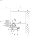
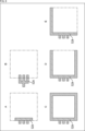
- FIG. 2 shows a schematic plan view of a pixel substrate 41 on which pixels 21 are formed and a control substrate 42 on which control circuits and signal processing circuits for pixels 21 are formed.
- the pixel array section 11 is formed on the pixel substrate 41 at the center of the chip-sized substrate. Furthermore, a plurality of pads 51 are formed on the outer periphery of the substrate outside the pixel array section 11 to serve as contact points with external devices. Each pad 51 of the pixel substrate 41 includes the output section 19 shown in FIG. 1, and is electrically connected to an external device by wire bonding or the like.
- the pads 51 of the pixel substrate 41 include a signal pad 51 to which signals such as pixel signals and control signals are supplied, and a power/ground pad 51 to which a power supply voltage or ground is supplied.
- the shape of the pad 51 is the same for signal use and power supply/ground use.
- the I/F circuit 18 and a plurality of pad wirings 52 are formed on the control board 42.
- the signal processing section 16, the system control section 15, etc. may be formed on the control board 42.
- the pad wiring 52 of the control board 42 is formed at a position corresponding to the pad 51 of the pixel board 41, and is a wiring on the control board 42 side that is electrically connected to the pad 51 located at the same planar position.
- the pad wiring 52 includes a pad wiring 52A (hereinafter referred to as signal pad wiring 52A) electrically connected to the pad 51 for signal use on the pixel substrate 41, and a pad 51 for power supply/ground use on the pixel substrate 41.
- the signal pad wiring 52A and the power/ground pad wiring 52B have different wiring pattern areas, for example.
- FIG. 3 is a cross-sectional view schematically showing the laminated structure of the pixel substrate 41 and the control board 42, and is a cross-sectional view of a portion corresponding to the signal pad wiring 52A.
- the upper pixel substrate 41 and the lower control substrate 42 are bonded together at a bonding surface indicated by a dashed line.
- a light condensing layer 61, a semiconductor substrate 62, and a wiring layer 63 are laminated in order from the top. Therefore, the light condensing layer 61 and the wiring layer 63 are placed on opposite sides of the semiconductor substrate 62 (with the semiconductor substrate 62 as a reference).
- a wiring layer 63 is formed on the front side of the semiconductor substrate 62, and a light collecting layer 61 is formed on the back side.
- An on-chip microlens 67, a color filter 68, etc. are formed on the light collecting layer 61.
- Light from the object that has entered the upper surface (incident surface) of the light collecting layer 61 is focused by an on-chip microlens 67 onto a photodiode (not shown) formed on the semiconductor substrate 62.
- the semiconductor substrate 62 is formed using, for example, a silicon substrate using silicon (Si) as a semiconductor.
- the material of the semiconductor substrate 62 may be, for example, a group IV semiconductor such as Ge, or a group III-V semiconductor such as GaAs, InP, or InGaAs.
- semiconductor elements such as a photodiode, a transfer gate, a charge-voltage conversion section (FD section), a reset gate, an amplification transistor, and a selection transistor of each pixel 21 are formed on the semiconductor substrate 62. ing.
- a plurality of layers of wiring 64 and an interlayer insulating film 65 are formed in the wiring layer 63.
- the wiring 64 in each layer is connected to the wiring 64 in the upper or lower layer through vias 66 in required areas.
- the wiring 64 and the via 66 are made of, for example, a metal material such as Cu or Al.
- pads 51 for external connection are formed in the wiring layer 63.
- the pad 51 is formed to have approximately the same height and thickness as the wiring 64 in the second to fourth layers of the wiring layer 63.
- a through hole 71 is formed above the pad 51 and penetrates the light collecting layer 61 and the semiconductor substrate 62 . Through this through hole 71, a part of the surface of the pad 51 on which the wire bond ball is formed (hereinafter referred to as a connection surface) is exposed.
- a via 73 is connected to the surface of the pad 51 opposite to the connection surface, and the pad 51 is connected to a pad 72 for bonding to the control board 42 via the via 73.
- the pad 72 is made of, for example, Cu.
- the pad 72 is connected to the pad 91 of the wiring layer 81 of the control board 42 by Cu--Cu bonding.
- a wiring layer 81 and a semiconductor substrate 82 are laminated in order from the top.
- the wiring layer 81 of the control board 42 is formed on the wiring layer 63 side of the pixel board 41, and the wiring layer 63 of the pixel board 41 and the wiring layer 81 of the control board 42 are in contact with each other.
- a plurality of layers of wiring 83 and an interlayer insulating film 84 are formed in the wiring layer 81.
- the wiring 83 in each layer is connected to the wiring 83 in the upper or lower layer by vias 85 in required areas.
- the wiring 83 and the via 85 are made of, for example, a metal material such as Cu or Al.
- a pad 91 for bonding to the pixel substrate 41 is formed at the upper end of the wiring layer 81.
- Pad 91 is made of, for example, Cu. Although a gap is left in FIG. 3 for clarity, the lower surface of the pad 72 of the pixel substrate 41 and the upper surface of the pad 91 of the control board 42 are connected by Cu--Cu bonding.
- a pad 91 on the control board 42 which is Cu-Cu bonded to a pad 72 on the pixel board 41 is connected to the signal pad wiring 52A in the uppermost layer in the wiring layer 81 via a via 92.
- a wiring 83A is provided at a predetermined position on the same layer as the signal pad wiring 52A, and the wiring 83A is connected to a lower layer wiring 83B via a via 85A.
- the semiconductor substrate 82 is formed of, for example, a silicon substrate, but similarly to the semiconductor substrate 62 described above, a material other than silicon may be used.
- the solid-state imaging device 1 in which the pixel substrate 41 and the control board 42 are stacked as described above is a back-illuminated MOS solid-state imaging device in which light enters from the back side of the semiconductor substrate 62.
- the pad 51 on the pixel board 41 side that outputs a pixel signal as an output signal is connected to the signal pad wiring 52A on the control board 42 side via the via 73, the pad 72, the pad 91, and the via 92. electrically connected.
- the signal pad wiring 52A, wiring 83A, wiring 83B, etc. have a structure that suppresses the influence of capacitance due to electrical characteristics, thereby increasing the speed of the communication interface. and wideband.
- the wiring structure within the wiring layer 81 on the control board 42 side that realizes high-speed and wide-band communication interface will be described in detail below.
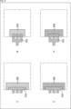
- FIG. 4 is a cross-sectional view showing details of the pad wiring structure in the wiring layer 81 on the control board 42 side connected to the signal pad 51 of the pixel board 41 in FIG.
- the pad 51 of the pixel board 41 is connected to the signal pad wiring 52A of the control board 42 via the via 73, the pad 72, the pad 91, and the via 92.
- the output signal SIG is supplied to the signal pad wiring 52A, and the output signal SIG is output from the pad 51 of the pixel substrate 41 to an external device via the pad 91, the pad 72, etc.
- the wiring 83A formed in the same layer as the signal pad wiring 52A is connected to the lower layer wiring 83B via the via 85A, and the lower layer wiring 83B is connected to the high resistance element 101 in the wiring layer 81 via the via 85B etc. , and is connected to the wiring 83C.
- a VSS potential (eg, GND) is supplied to the wiring 83C.
- the VSS potential is also supplied to the wirings 83A and 83B via the high resistance element 101, and the wirings 83A and 83B constitute shield wiring.
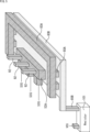
- FIG. 5 is a perspective view showing a specific example of the arrangement of a signal pad wiring 52A to which the output signal SIG is input, and wirings 83A and 83B formed as shield wirings around the signal pad wiring 52A. Note that in FIG. 5, the patterns of the wirings 83A, 83B, etc. are shown different from those in FIG. 4 in order to make the diagram easier to understand.
- the signal pad wiring 52A to which the output signal SIG is input is formed with a smaller planar area than the pad 51 of the pixel substrate 41 within a range that allows the current value of the output signal SIG.
- the signal pad wiring 52A is formed in the shape of three comb teeth, and three vias 92 are also formed for connection to the upper layer pad 91 (FIG. 4).
- the area may be formed in accordance with the current value of the output signal SIG, and is not limited to this example.
- the wiring 83A is arranged in the same layer as the signal pad wiring 52A so as to surround the signal pad wiring 52A, and the wiring 83B is formed at a position overlapping the signal pad wiring 52A and the wiring 83A in plan view.
- Wiring 83B is connected to high resistance element 101 via one or more vias (including via 85B).
- the pad 51 of the pixel substrate 41 in FIG. 4 is formed with a thickness and area that can withstand the stress of the wire bond ball. Since the pad 51 of the pixel board 41 has sufficient stress resistance, the signal pad wiring 52A on the control board 42 side connected to the pad 51 only needs to have current resistance for the output signal SIG. It can be formed with the minimum planar area that allows the current value.
- Capacitances 102A and 102B which are pad coupling capacitances, occur between the signal pad wiring 52A and the adjacent wirings 83A and 83B in the same layer or lower layer, but by forming the signal pad wiring 52A with the minimum area, the pad The coupling capacitance can be reduced. Further, by feeding the VSS potential to the wirings 83A and 83B via the high resistance element 101, the shield capacitance (capacitances 102A and 102B) can be nullified.
- a parasitic capacitance 103 that occurs between the upper and lower wirings 83 occurs between the wiring 83B and the well region 111 (or P sub-substrate region) of the semiconductor substrate 82, but this parasitic capacitance 103 also has a high It can be nullified by supplying the VSS potential through the resistance element 101.
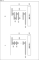
- a in FIG. 6 is an RC circuit (hereinafter referred to as the present RC circuit) corresponding to the present method of feeding the VSS potential to the shield wiring via the high-resistance element 101, and B in FIG.
- This is an RC circuit as a comparative example (hereinafter referred to as a comparative RC circuit) without the high resistance element 101 or shield wiring.
- the resistor 151 is the wiring resistance of the signal pad wiring 52A, etc.
- the capacitor 152 is the capacitance 102A and 102B of the shield wiring (wirings 83A and 83B)
- the resistor 153 is the high resistance Corresponds to element 101.
- Resistor 155 is a terminating resistor.
- the voltage waveform V M1 at the output end 154 in this RC circuit can be expressed as in the equation shown in FIG.
- a resistor 151' is a wiring resistance such as the signal pad wiring 52A, and a capacitor 152' corresponds to the parasitic capacitance 103 generated between the signal pad wiring 52A and the wiring 83.
- Resistor 155 is a terminating resistor.
- the voltage waveform V M2 at the output terminal 154 in the comparison RC circuit can be expressed as in the equation shown in FIG.
- the conditions of this RC circuit and the comparative RC circuit are the same except for the resistor 153 corresponding to the high resistance element 101.
- the resistance value R 0 of the resistor 151 is 50 ⁇
- the capacitance C of the capacitors 152 and 152' is 1.0 pF
- the resistance value R L of the resistor 155 which is the terminating resistor, is 50 ⁇ .
- the resistance value Rp of the resistor 153 is 500 ⁇ .
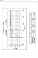
- FIG. 7 shows the signal waveforms output from the output terminals 154 of each of the present RC circuit and the comparative RC circuit.
- the transition time is significantly shortened compared to the comparative RC circuit.
- the effective capacitance component can be made to appear small like a low-pass filter in the frequency band where high-speed interface communication is performed. This makes it possible to increase the data rate and realize a faster communication interface.
- the resistance value Rp of the high-resistance element 101 corresponding to the resistor 153 is appropriately set according to the communication frequency of the high-speed interface.
- the signal pad wiring 52A on the control board 42 side does not need to have a uniform pattern shape as long as the current value of the output signal SIG is allowed, and can be formed in a planar shape suitable for each application. .
- the wiring pattern (planar shape) of the signal pad wiring 52A may be determined according to the impedance allowed for connection with the signal pad 51 of the pixel substrate 41, etc.
- a to E in FIG. 8 show examples of wiring patterns of the signal pad wiring 52A.
- a rectangle indicated by a dashed dotted line indicates a formation area of the pad 51 on the pixel substrate 41 side that is connected to the signal pad wiring 52A.
- FIG. 8A is a plan view of the wiring pattern of the signal pad wiring 52A shown in FIG. 5.
- the signal pad wiring 52A is composed of three comb-shaped patterns and one linear pattern connected perpendicularly to the three comb-shaped patterns.
- FIG. 8B is a plan view showing another example of the wiring pattern of the signal pad wiring 52A.
- the signal pad wiring 52A shown in FIG. 8B is composed of three comb-shaped patterns.
- FIG. 8C is a plan view showing another example of the wiring pattern of the signal pad wiring 52A.
- the signal pad wiring 52A in FIG. 8C is composed of three linear patterns and a rectangular pattern with a predetermined line width formed along the outer periphery of the rectangular pad 51 on the pixel substrate 41 side. Ru.
- FIG. 8D is a plan view showing another example of the wiring pattern of the signal pad wiring 52A.
- the signal pad wiring 52A shown in D in FIG. 8 includes three linear patterns and a U-shaped pattern with a predetermined line width formed along three sides of the rectangular pad 51 on the pixel substrate 41 side. configured.
- FIG. 8E is a plan view showing another wiring pattern example of the signal pad wiring 52A.
- the signal pad wiring 52A shown in E of FIG. 8 includes three linear patterns and an L-shaped pattern with a predetermined line width formed along two sides of the rectangular pad 51 on the pixel substrate 41 side. configured.
- the wiring pattern of the signal pad wiring 52A may have a pattern shape other than the examples shown in FIGS. 8A to 8E.
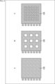
- FIGS. 9A to 9D show examples of the wiring pattern of the wiring 83B arranged under the signal pad wiring 52A to which the output signal SIG is input.
- the wiring pattern of the signal pad wiring 52A is also shown superimposed, and the wiring pattern of A or B of FIG. 8 is adopted as the wiring pattern of the signal pad wiring 52A.
- a rectangle indicated by a chain line indicates a formation area of the pad 51 on the pixel substrate 41 side.
- the wiring pattern of the wiring 83B arranged under the signal pad wiring 52A may be a solid film pattern as shown in A and B of FIG. 9, or a mesh pattern (lattice pattern) as shown in C and D of FIG. ) etc.
- the pattern area of the wiring 83B is different between A and B in FIG. Similarly, in C and D in FIG. 9, the pattern area of the wiring 83B is different.
- the wiring pattern of the wiring 83B that determines the potential of the capacitor 102B is appropriately determined according to the communication frequency of the output signal SIG.
- FIGS. 10A and 10B show an example of a wiring pattern of a wiring 83A arranged in the same layer as the signal pad wiring 52A to which the output signal SIG is input.
- 10A and 10B also show the wiring patterns of the signal pad wiring 52A and the lower layer wiring 83B.
- the wiring pattern shown in FIG. 9A is used as the wiring pattern of the signal pad wiring 52A and the wiring 83B, but it goes without saying that other wiring patterns may be used.
- a rectangle indicated by a chain line indicates a region where the pad 51 is formed on the pixel substrate 41 side.
- the wiring pattern of the wiring 83A is a U-shaped pattern as shown in A in FIG. 10, which surrounds the signal pad wiring 52A to which the output signal SIG is input in three directions, horizontally and vertically. be able to.
- an I-shaped (linear) pattern shape as shown in FIG. 10B may be used.
- the wiring pattern of the wiring 83A that determines the potential of the capacitor 102A is appropriately determined according to the communication frequency of the output signal SIG.
- FIG. 8 shows an example of the wiring pattern of the signal pad wiring 52A
- FIG. 9 shows an example of the wiring pattern of the wiring 83B in the same layer as the signal pad wiring 52A
- FIG. An example of a wiring pattern is shown.
- the combination of the wiring patterns of the signal pad wiring 52A, the wiring 83A, and the wiring 83B can be arbitrarily selected, and pattern shapes other than those illustrated may be adopted.
- both the wiring 83A and the wiring 83B as shield wiring are arranged around the signal pad wiring 52A to which the output signal SIG is input, but the wiring 83A on the same layer as the signal pad wiring 52A is Alternatively, only one of the lower layer wirings 83B may be provided.
- the pad wiring 52 connected to the pad 51 of the pixel substrate 41 includes a power/ground pad wiring 52B in addition to the signal pad wiring 52A.
- FIG. 11 show examples of wiring patterns of the power supply/ground pad wiring 52B.
- rectangles indicated by one-dot chain lines (which overlap in many parts) indicate the formation area of the pad 51 on the pixel substrate 41 side.
- the power supply/ground pad wiring 52B is required to flow a sufficient current, so it is formed to have a high pattern density so as to have low impedance.
- the power/ground pad wiring 52B is formed in a rectangular pattern having the same size as the pad 51 on the pixel substrate 41 side, as shown in FIG. 11A.
- the power supply/ground pad wiring 52B may be a mesh pattern with a thick line width as shown in B of FIG. 11, or a mesh pattern with a thin line width but many lines as shown in C of FIG. 11. may be formed. Pattern shapes other than the wiring patterns illustrated in FIGS. 11A to 11C may also be employed.
- the wiring pattern of the power supply/ground pad wiring 52B is formed with a larger planar area and pattern density than the signal pad wiring 52A for signal use.
- the high resistance element 101 can be composed of a parasitic resistance due to a stacked via 201 formed in the wiring layer 81 and a metal resistance 202.
- the stacked via 201 is composed of multiple layers of wiring 83 and vias 85 that connect the upper and lower wirings 83, and the number of stacked wirings 83 and the number of vias 85 can be determined as appropriate.
- the metal resistor 202 may be replaced with a polysilicon resistor using polysilicon.
- the high-resistance element 101 is composed of a parasitic resistance caused by a stacked via 201 formed in a wiring layer 81 and a diffused resistance 203 formed by a diffusion layer of a semiconductor substrate 82. be able to.
- the high resistance element 101 may be configured only with parasitic resistance due to stacked vias 201 formed in the wiring layer 81, as shown in FIG. 13A.
- the high resistance element 101 may be configured with a parasitic resistance formed by a combination of a thin wiring 83' and a stacked via 201.
- the high resistance element 101 can be realized in a small area.
- VSS potential for example, GND
- GND GND
- the potential supplied to the wirings 83A and 83B via the high resistance element 101 may be different from the VSS potential. More specifically, a Vcom potential higher than the VSS potential (Vcom>VSS) can be supplied to the wirings 83A and 83B via the high resistance element 101.
- FIG. 14 shows the signal pad wiring 52A and the I/F circuit 18 that outputs the output signal SIG when the VSS potential is supplied to the wirings 83A and 83B as shield wirings. Note that the output signal SIG is a differential signal.
- the Vouth potential generated by the regulator 251 and the VSS potential are supplied to the driver 252.
- the driver 252 generates an output signal SIG, which is a differential signal in which the VSS potential is an OFF potential and the Vouth potential is an ON potential, and outputs each to the signal pad wiring 52A.
- SIG an output signal in which the VSS potential is an OFF potential and the Vouth potential is an ON potential
- FIG. 15 shows the signal pad wiring 52A and the I/F circuit 18 that outputs the output signal SIG when the Vcom potential is supplied to the wirings 83A and 83B as shield wirings.
- the capacitance 102 that is the pad coupling capacitance will be lower than the Vcom potential. Since the noise is separated from the noise of the semiconductor substrate 82, the noise is not superimposed on the output signal SIG and causes jitter.
- FIG. 16 shows the signal pad wiring 52A and the I/F that outputs the output signal SIG when the ON and OFF potentials of the output signal SIG are generated based on the Vcom potential instead of the VSS potential. Circuit 18 is shown.
- the regulator 251H In the I/F circuit 18, the regulator 251H generates a Vouth potential that is an ON potential and supplies it to the driver 252.
- the regulator 251L generates a Voutl potential, which is an OFF potential, and supplies it to the driver 252.
- the driver 252 generates an output signal SIG, which is a differential signal in which the Voutl potential is an OFF potential and the Vouth potential is an ON potential, and outputs each to the signal pad wiring 52A. If noise is included in the well at the VSS potential of the semiconductor substrate 82, the noise will not be in the same phase as fluctuations in the output signal SIG, and will therefore be superimposed on the output signal SIG as jitter.
- FIG. 17 shows the signal pad wiring 52A and the signal pad wiring 52A when generating the ON potential and OFF potential of the output signal SIG based on the Vcom potential and supplying the Vcom potential to the wirings 83A and 83B as shield wirings, and outputting the output signal SIG.
- An I/F circuit 18 is shown.
- the output signal SIG is generated based on the Vcom potential and the Vcom potential is supplied to the wirings 83A and 83B as shield wirings, even if the well at the VSS potential of the semiconductor substrate 82 contains noise, Since the capacitor 102, which is a pad coupling capacitor, is coupled to the Vcom potential, it is separated from the noise of the semiconductor substrate 82, and the noise is not superimposed on the output signal SIG to cause jitter.
- the VSS potential (for example, GND) may be supplied to the wirings 83A and 83B as shield wirings via the high resistance element 101, but the Vcom potential (Vcom>VSS ), it is possible to prevent VSS noise from being superimposed on the output signal SIG.
- the signal pad wiring 52A With a planar area as small as possible to allow the current value of the output signal SIG, the space of the wiring layer 81 is freed, and the degree of freedom of the wiring 83 is improved. Utilizing this, by supplying a Vcom potential different from the VSS potential to the wirings 83A and 83B as shield wirings, it is possible to reduce the charging and discharging charges of the pad coupling capacitance.
- FIG. 18 is a diagram showing an example of use of an image sensor using the solid-state imaging device 1 described above.
- the solid-state imaging device 1 described above can be used as an image sensor in various cases for sensing light such as visible light, infrared light, ultraviolet light, and X-rays, for example, as described below.
- ⁇ Digital cameras, mobile devices with camera functions, and other devices that take images for viewing purposes Devices used for transportation, such as in-vehicle sensors that take pictures of the rear, surroundings, and interior of the car, surveillance cameras that monitor moving vehicles and roads, and distance sensors that measure the distance between vehicles, etc.
- Devices used for transportation such as in-vehicle sensors that take pictures of the rear, surroundings, and interior of the car, surveillance cameras that monitor moving vehicles and roads, and distance sensors that measure the distance between vehicles, etc.
- User gestures Devices used in home appliances such as TVs, refrigerators, and air conditioners to take pictures and operate devices according to the gestures.
- - Endoscopes devices that perform blood vessel imaging by receiving infrared light, etc.
- Devices used for medical and healthcare purposes - Devices used for security, such as surveillance cameras for crime prevention and cameras for person authentication - Skin measurement devices that take pictures of the skin, and devices that take pictures of the scalp - Devices used for beauty purposes, such as microscopes for skin care.
- - Devices used for sports such as action cameras and wearable cameras.
- - Cameras, etc. used to monitor the condition of fields and crops. , equipment used for agricultural purposes
- the technology of the present disclosure is not limited to application to solid-state imaging devices. That is, the technology of the present disclosure applies to an image capture unit (photoelectric conversion unit) in an image capture device such as a digital still camera or a video camera, a mobile terminal device having an image capture function, or a copying machine that uses a solid-state image capture device in an image reading unit. ) is applicable to all electronic devices that use solid-state imaging devices.
- the solid-state imaging device may be formed as a single chip, or may be a module having an imaging function in which an imaging section and a signal processing section or an optical system are packaged together.
- FIG. 19 is a block diagram showing a configuration example of an imaging device as an electronic device to which the technology of the present disclosure is applied.
- the imaging device 300 in FIG. 19 includes an optical section 301 including a lens group, a solid-state imaging device (imaging device) 302 in which the configuration of the solid-state imaging device 1 in FIG. 1 is adopted, and a DSP (Digital Signal (processor) circuit 303.
- the imaging device 300 also includes a frame memory 304, a display section 305, a recording section 306, an operation section 307, and a power supply section 308.
- the DSP circuit 303, frame memory 304, display section 305, recording section 306, operation section 307, and power supply section 308 are interconnected via a bus line 309.
- the optical section 301 takes in incident light (image light) from a subject and forms an image on the imaging surface of the solid-state imaging device 302.
- the solid-state imaging device 302 converts the amount of incident light that is imaged on the imaging surface by the optical section 301 into an electrical signal for each pixel, and outputs the electric signal as a pixel signal.
- a shield wiring (wiring 83A or 83B) is arranged around the signal pad wiring 52A of the solid-state imaging device 1 of FIG. 1, that is, the control board 42 side to which the output signal SIG is supplied, and a high resistance
- a solid-state imaging device in which a predetermined potential (VSS potential or Vcom potential) is supplied via the element 101 can be used.
- the display unit 305 is configured with a thin display such as an LCD (Liquid Crystal Display) or an organic EL (Electro Luminescence) display, and displays moving images or still images captured by the solid-state imaging device 302.
- the recording unit 306 records a moving image or a still image captured by the solid-state imaging device 302 on a recording medium such as a hard disk or a semiconductor memory.
- the operation unit 307 issues operation commands regarding various functions of the imaging device 300 under operation by the user.
- the power supply section 308 appropriately supplies various kinds of power to serve as operating power for the DSP circuit 303, frame memory 304, display section 305, recording section 306, and operation section 307 to these supply targets.
- the solid-state imaging device 302 As described above, by employing the configuration of the solid-state imaging device 1 described above as the solid-state imaging device 302, it is possible to realize a faster communication interface. Therefore, it is possible to increase the speed of captured images even in the imaging device 300 such as a video camera, a digital still camera, or a camera module for mobile devices such as a mobile phone.
- the imaging device 300 such as a video camera, a digital still camera, or a camera module for mobile devices such as a mobile phone.
- the technology according to the present disclosure (this technology) can be applied to various products.
- the technology according to the present disclosure may be realized as a device mounted on any type of moving body such as a car, electric vehicle, hybrid electric vehicle, motorcycle, bicycle, personal mobility, airplane, drone, ship, robot, etc. It's okay.
- FIG. 20 is a block diagram illustrating a schematic configuration example of a vehicle control system, which is an example of a mobile body control system to which the technology according to the present disclosure can be applied.
- the vehicle control system 12000 includes a plurality of electronic control units connected via a communication network 12001.
- the vehicle control system 12000 includes a drive system control unit 12010, a body system control unit 12020, an outside vehicle information detection unit 12030, an inside vehicle information detection unit 12040, and an integrated control unit 12050.
- a microcomputer 12051, an audio/image output section 12052, and an in-vehicle network I/F (interface) 12053 are illustrated.
- the drive system control unit 12010 controls the operation of devices related to the drive system of the vehicle according to various programs.
- the drive system control unit 12010 includes a drive force generation device such as an internal combustion engine or a drive motor that generates drive force for the vehicle, a drive force transmission mechanism that transmits the drive force to wheels, and a drive force transmission mechanism that controls the steering angle of the vehicle. It functions as a control device for a steering mechanism to adjust and a braking device to generate braking force for the vehicle.
- the body system control unit 12020 controls the operations of various devices installed in the vehicle body according to various programs.
- the body system control unit 12020 functions as a keyless entry system, a smart key system, a power window device, or a control device for various lamps such as a headlamp, a back lamp, a brake lamp, a turn signal, or a fog lamp.
- radio waves transmitted from a portable device that replaces a key or signals from various switches may be input to the body control unit 12020.
- the body system control unit 12020 receives input of these radio waves or signals, and controls the door lock device, power window device, lamp, etc. of the vehicle.
- the external information detection unit 12030 detects information external to the vehicle in which the vehicle control system 12000 is mounted.
- an imaging section 12031 is connected to the outside-vehicle information detection unit 12030.
- the vehicle exterior information detection unit 12030 causes the imaging unit 12031 to capture an image of the exterior of the vehicle, and receives the captured image.
- the external information detection unit 12030 may perform object detection processing such as a person, car, obstacle, sign, or text on the road surface or distance detection processing based on the received image.
- the imaging unit 12031 is an optical sensor that receives light and outputs an electrical signal according to the amount of received light.
- the imaging unit 12031 can output the electrical signal as an image or as distance measurement information.
- the light received by the imaging unit 12031 may be visible light or non-visible light such as infrared rays.
- the in-vehicle information detection unit 12040 detects in-vehicle information.
- a driver condition detection section 12041 that detects the condition of the driver is connected to the in-vehicle information detection unit 12040.
- the driver condition detection unit 12041 includes, for example, a camera that images the driver, and the in-vehicle information detection unit 12040 detects the degree of fatigue or concentration of the driver based on the detection information input from the driver condition detection unit 12041. It may be calculated, or it may be determined whether the driver is falling asleep.
- the microcomputer 12051 calculates control target values for the driving force generation device, steering mechanism, or braking device based on the information inside and outside the vehicle acquired by the vehicle exterior information detection unit 12030 or the vehicle interior information detection unit 12040, Control commands can be output to 12010.
- the microcomputer 12051 realizes ADAS (Advanced Driver Assistance System) functions, including vehicle collision avoidance or impact mitigation, following distance based on vehicle distance, vehicle speed maintenance, vehicle collision warning, vehicle lane departure warning, etc. It is possible to perform cooperative control for the purpose of ADAS (Advanced Driver Assistance System) functions, including vehicle collision avoidance or impact mitigation, following distance based on vehicle distance, vehicle speed maintenance, vehicle collision warning, vehicle lane departure warning, etc. It is possible to perform cooperative control for the purpose of
- ADAS Advanced Driver Assistance System
- the microcomputer 12051 controls the driving force generating device, steering mechanism, braking device, etc. based on information about the surroundings of the vehicle acquired by the vehicle exterior information detection unit 12030 or the vehicle interior information detection unit 12040. It is possible to perform cooperative control for the purpose of autonomous driving, etc., which does not rely on operation.
- the microcomputer 12051 can output a control command to the body system control unit 12020 based on the information outside the vehicle acquired by the outside information detection unit 12030.
- the microcomputer 12051 controls the headlamps according to the position of the preceding vehicle or oncoming vehicle detected by the vehicle exterior information detection unit 12030, and performs cooperative control for the purpose of preventing glare, such as switching from high beam to low beam. It can be carried out.
- the audio and image output unit 12052 transmits an output signal of at least one of audio and images to an output device that can visually or audibly notify information to the occupants of the vehicle or to the outside of the vehicle.
- an audio speaker 12061, a display section 12062, and an instrument panel 12063 are illustrated as output devices.
- the display unit 12062 may include, for example, at least one of an on-board display and a head-up display.
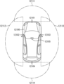
- FIG. 21 is a diagram showing an example of the installation position of the imaging section 12031.
- the vehicle 12100 has imaging units 12101, 12102, 12103, 12104, and 12105 as the imaging unit 12031.
- the imaging units 12101, 12102, 12103, 12104, and 12105 are provided, for example, at positions such as the front nose, side mirrors, rear bumper, back door, and the top of the windshield inside the vehicle 12100.
- An imaging unit 12101 provided in the front nose and an imaging unit 12105 provided above the windshield inside the vehicle mainly acquire images in front of the vehicle 12100.
- Imaging units 12102 and 12103 provided in the side mirrors mainly capture images of the sides of the vehicle 12100.
- An imaging unit 12104 provided in the rear bumper or back door mainly captures images of the rear of the vehicle 12100.
- the images of the front acquired by the imaging units 12101 and 12105 are mainly used for detecting preceding vehicles, pedestrians, obstacles, traffic lights, traffic signs, lanes, and the like.
- FIG. 21 shows an example of the imaging range of the imaging units 12101 to 12104.
- An imaging range 12111 indicates the imaging range of the imaging unit 12101 provided on the front nose
- imaging ranges 12112 and 12113 indicate imaging ranges of the imaging units 12102 and 12103 provided on the side mirrors, respectively
- an imaging range 12114 shows the imaging range of the imaging unit 12101 provided on the front nose.
- the imaging range of the imaging unit 12104 provided in the rear bumper or back door is shown. For example, by overlapping the image data captured by the imaging units 12101 to 12104, an overhead image of the vehicle 12100 viewed from above can be obtained.
- At least one of the imaging units 12101 to 12104 may have a function of acquiring distance information.
- at least one of the imaging units 12101 to 12104 may be a stereo camera including a plurality of image sensors, or may be an image sensor having pixels for phase difference detection.
- the microcomputer 12051 determines the distance to each three-dimensional object within the imaging ranges 12111 to 12114 and the temporal change in this distance (relative speed with respect to the vehicle 12100) based on the distance information obtained from the imaging units 12101 to 12104. In particular, by determining the three-dimensional object that is closest to the vehicle 12100 on its path and that is traveling at a predetermined speed (for example, 0 km/h or more) in approximately the same direction as the vehicle 12100, it is possible to extract the three-dimensional object as the preceding vehicle. can.
- a predetermined speed for example, 0 km/h or more
- the microcomputer 12051 can set an inter-vehicle distance to be secured in advance in front of the preceding vehicle, and perform automatic brake control (including follow-up stop control), automatic acceleration control (including follow-up start control), and the like. In this way, it is possible to perform cooperative control for the purpose of autonomous driving, etc., in which the vehicle travels autonomously without depending on the driver's operation.
- the microcomputer 12051 transfers three-dimensional object data to other three-dimensional objects such as two-wheeled vehicles, regular vehicles, large vehicles, pedestrians, and utility poles based on the distance information obtained from the imaging units 12101 to 12104. It can be classified and extracted and used for automatic obstacle avoidance. For example, the microcomputer 12051 identifies obstacles around the vehicle 12100 into obstacles that are visible to the driver of the vehicle 12100 and obstacles that are difficult to see. Then, the microcomputer 12051 determines a collision risk indicating the degree of risk of collision with each obstacle, and when the collision risk exceeds a set value and there is a possibility of a collision, the microcomputer 12051 transmits information via the audio speaker 12061 and the display unit 12062. By outputting a warning to the driver via the vehicle control unit 12010 and performing forced deceleration and avoidance steering via the drive system control unit 12010, driving support for collision avoidance can be provided.
- the microcomputer 12051 determines a collision risk indicating the degree of risk of collision with each obstacle, and when the collision risk exceed
- At least one of the imaging units 12101 to 12104 may be an infrared camera that detects infrared rays.
- the microcomputer 12051 can recognize a pedestrian by determining whether the pedestrian is present in the images captured by the imaging units 12101 to 12104.
- pedestrian recognition involves, for example, a procedure for extracting feature points in images captured by the imaging units 12101 to 12104 as infrared cameras, and a pattern matching process is performed on a series of feature points indicating the outline of an object to determine whether it is a pedestrian or not.
- the audio image output unit 12052 creates a rectangular outline for emphasis on the recognized pedestrian.
- the display unit 12062 is controlled to display the .
- the audio image output unit 12052 may control the display unit 12062 to display an icon or the like indicating a pedestrian at a desired position.
- the technology according to the present disclosure can be applied to the imaging unit 12031 among the configurations described above.
- the solid-state imaging device 1 described above can be applied as the imaging section 12031.
- the present disclosure is not limited to application to a solid-state imaging device that detects the distribution of the incident amount of visible light and captures the image as an image, but also applies to a solid-state imaging device that captures the distribution of the incident amount of infrared rays, X-rays, particles, etc. as an image. It can be applied to all solid-state imaging devices (physical quantity distribution detection devices) such as imaging devices and, in a broader sense, fingerprint detection sensors that detect the distribution of other physical quantities such as pressure and capacitance and capture the images as images. be.
- the technology of the present disclosure is applicable not only to solid-state imaging devices but also to all semiconductor devices having other semiconductor integrated circuits.
- the technology of the present disclosure can take the following configuration.
- (1) It is constructed by laminating a pixel substrate on which pixels are formed and a control board,
- the pixel substrate has a pad that serves as a contact point with an external device,
- the control board is a signal pad wiring connected to the pad; a shield wiring arranged around the signal pad wiring;
- a solid-state imaging device comprising: a high resistance element connected to the shield wiring.
- the solid-state imaging device according to any one of (1) to (4), wherein the shield wiring is arranged in at least one of the same layer or a lower layer as the signal pad wiring.
- the high-resistance element includes a metal resistor or a polysilicon resistor.
- the high-resistance element includes a diffused resistor.
- the high resistance element includes a well resistance.
- the solid-state imaging device according to any one of (1) to (8), wherein the high-resistance element includes a parasitic resistance due to a stacked via.
- the solid-state imaging device according to any one of (1) to (8), wherein the high-resistance element includes a parasitic resistance due to stacked vias and thin wiring.
- the signal pad wiring has a smaller planar area than the pad.
- the pad includes a first pad that outputs a pixel signal of the pixel and a second pad that is supplied with a power supply voltage or ground.
- It is constructed by laminating a pixel substrate on which pixels are formed and a control board, The pixel substrate has a pad that serves as a contact point with an external device, The control board is a signal pad wiring connected to the pad; a shield wiring arranged around the signal pad wiring;
- An electronic device comprising: a solid-state imaging device comprising: a high resistance element connected to the shield wiring;
- Solid-state imaging device 18 I/F circuit, 21 pixels, 41 pixel board, 42 control board, 51 pad, 52 pad wiring, 52A pad wiring, 52B pad wiring, 62 semiconductor substrate, 71 penetration Hole, 72 pad, 73 via , 81 wiring layer, 82 semiconductor substrate, 83, 83A, 83B, 83C wiring, 84 interlayer insulating film, 85, 85A, 85B via, 101 high resistance element, 102, 102A, 102B capacitor, 103 Raw capacity, 111 well area, 201 Stacked via, 202 Metal resistance, 203 Diffused resistance, 204 P well, 207 P well resistance, 211 N well, 214 N well resistance, 251 Regulator, 251H Regulator, 251L Regulator, 252 driver, 300 imaging device, 302 solid-state imaging device
Landscapes
- Engineering & Computer Science (AREA)
- Physics & Mathematics (AREA)
- Multimedia (AREA)
- Signal Processing (AREA)
- Electromagnetism (AREA)
- Power Engineering (AREA)
- Condensed Matter Physics & Semiconductors (AREA)
- General Physics & Mathematics (AREA)
- Computer Hardware Design (AREA)
- Microelectronics & Electronic Packaging (AREA)
- Solid State Image Pick-Up Elements (AREA)
Abstract
Cette divulgation concerne un dispositif d'imagerie à semi-conducteurs et un appareil électronique avec lesquels il est possible d'obtenir une vitesse accrue pour une interface de communication. Ce dispositif d'imagerie à semi-conducteurs est conçu en stratifiant un substrat de commande et un substrat de pixel sur lequel des pixels sont formés. Le substrat de pixel présente un plot qui sert de contact avec un dispositif externe. Le substrat de commande comprend : un câblage de plot de signal connecté au plot ; une ligne de câblage de blindage placée à la périphérie de la ligne de câblage de plot de signal ; et un élément à haute résistance connecté à la ligne de câblage de blindage. Cette divulgation peut, par exemple, être appliquée à un dispositif d'imagerie à semi-conducteurs ou similaire.
Applications Claiming Priority (2)
| Application Number | Priority Date | Filing Date | Title |
|---|---|---|---|
| JP2022072882 | 2022-04-27 | ||
| JP2022-072882 | 2022-04-27 |
Publications (1)
| Publication Number | Publication Date |
|---|---|
| WO2023210324A1 true WO2023210324A1 (fr) | 2023-11-02 |
Family
ID=88518787
Family Applications (1)
| Application Number | Title | Priority Date | Filing Date |
|---|---|---|---|
| PCT/JP2023/014547 WO2023210324A1 (fr) | 2022-04-27 | 2023-04-10 | Dispositif d'imagerie à semi-conducteurs et appareil électronique |
Country Status (1)
| Country | Link |
|---|---|
| WO (1) | WO2023210324A1 (fr) |
Citations (4)
| Publication number | Priority date | Publication date | Assignee | Title |
|---|---|---|---|---|
| JPH10321804A (ja) * | 1997-03-14 | 1998-12-04 | Toshiba Corp | マイクロ波集積回路素子 |
| JP2007194981A (ja) * | 2006-01-20 | 2007-08-02 | Sony Corp | 物理情報取得方法および物理情報取得装置ならびに駆動装置 |
| JP2012089739A (ja) * | 2010-10-21 | 2012-05-10 | Sony Corp | 固体撮像装置及び電子機器 |
| JP2020141397A (ja) * | 2019-02-25 | 2020-09-03 | キヤノン株式会社 | 半導体装置および機器 |
-
2023
- 2023-04-10 WO PCT/JP2023/014547 patent/WO2023210324A1/fr unknown
Patent Citations (4)
| Publication number | Priority date | Publication date | Assignee | Title |
|---|---|---|---|---|
| JPH10321804A (ja) * | 1997-03-14 | 1998-12-04 | Toshiba Corp | マイクロ波集積回路素子 |
| JP2007194981A (ja) * | 2006-01-20 | 2007-08-02 | Sony Corp | 物理情報取得方法および物理情報取得装置ならびに駆動装置 |
| JP2012089739A (ja) * | 2010-10-21 | 2012-05-10 | Sony Corp | 固体撮像装置及び電子機器 |
| JP2020141397A (ja) * | 2019-02-25 | 2020-09-03 | キヤノン株式会社 | 半導体装置および機器 |
Similar Documents
| Publication | Publication Date | Title |
|---|---|---|
| US11688747B2 (en) | Solid-state imaging device and electronic apparatus | |
| CN110383481B (zh) | 固态成像装置和电子设备 | |
| JP7370413B2 (ja) | 固体撮像装置、及び電子機器 | |
| US20230238404A1 (en) | Solid-state imaging device and electronic apparatus | |
| WO2019093150A1 (fr) | Élément de capture d'image et appareil électronique | |
| US20210314516A1 (en) | Solid-state image capturing device, method of driving solid-state image capturing device, and electronic apparatus | |
| US11863892B2 (en) | Imaging unit and electronic apparatus with first and second light blocking films | |
| JP7383633B2 (ja) | 固体撮像素子、固体撮像素子パッケージ、及び、電子機器 | |
| US20210385394A1 (en) | Solid-state imaging apparatus and electronic | |
| WO2020045142A1 (fr) | Dispositif d'imagerie et instrument électronique | |
| US20230013149A1 (en) | Solid-state image pickup device and electronic apparatus | |
| WO2019078291A1 (fr) | Dispositif d'imagerie | |
| WO2019207927A1 (fr) | Antenne réseau, dispositif d'imagerie à semi-conducteurs et appareil électronique | |
| WO2023210324A1 (fr) | Dispositif d'imagerie à semi-conducteurs et appareil électronique | |
| CN114008783A (zh) | 摄像装置 | |
| WO2023238924A1 (fr) | Dispositif à semi-conducteur et dispositif d'imagerie | |
| WO2022244328A1 (fr) | Dispositif d'imagerie à semi-conducteurs et appareil électronique | |
| WO2023243222A1 (fr) | Dispositif d'imagerie | |
| US11997400B2 (en) | Imaging element and electronic apparatus | |
| WO2023002592A1 (fr) | Élément d'imagerie à semi-conducteurs, son procédé de fabrication et appareil électronique | |
| WO2022172642A1 (fr) | Élément d'imagerie à semi-conducteur, procédé d'imagerie et dispositif électronique | |
| WO2023132151A1 (fr) | Élément de capture d'image et dispositif électronique | |
| WO2022201802A1 (fr) | Dispositif d'imagerie à semi-conducteurs et dispositif électronique | |
| WO2024043068A1 (fr) | Élément d'imagerie à semi-conducteurs et dispositif électronique | |
| WO2024038757A1 (fr) | Dispositif à semi-conducteurs et équipement électronique |
Legal Events
| Date | Code | Title | Description |
|---|---|---|---|
| 121 | Ep: the epo has been informed by wipo that ep was designated in this application |
Ref document number: 23796070 Country of ref document: EP Kind code of ref document: A1 |