WO2023210324A1 - Solid-state imaging device and electronic apparatus - Google Patents
Solid-state imaging device and electronic apparatus Download PDFInfo
- Publication number
- WO2023210324A1 WO2023210324A1 PCT/JP2023/014547 JP2023014547W WO2023210324A1 WO 2023210324 A1 WO2023210324 A1 WO 2023210324A1 JP 2023014547 W JP2023014547 W JP 2023014547W WO 2023210324 A1 WO2023210324 A1 WO 2023210324A1
- Authority
- WO
- WIPO (PCT)
- Prior art keywords
- wiring
- pad
- solid
- state imaging
- imaging device
- Prior art date
Links
- 238000003384 imaging method Methods 0.000 title claims abstract description 131
- 239000000758 substrate Substances 0.000 claims abstract description 88
- 230000003071 parasitic effect Effects 0.000 claims description 12
- 238000010030 laminating Methods 0.000 claims description 5
- 239000002184 metal Substances 0.000 claims description 5
- 229910052751 metal Inorganic materials 0.000 claims description 5
- 229910021420 polycrystalline silicon Inorganic materials 0.000 claims description 4
- 229920005591 polysilicon Polymers 0.000 claims description 4
- 238000004891 communication Methods 0.000 abstract description 15
- 239000010410 layer Substances 0.000 description 59
- 238000012545 processing Methods 0.000 description 33
- 239000004065 semiconductor Substances 0.000 description 31
- 238000001514 detection method Methods 0.000 description 25
- 238000010586 diagram Methods 0.000 description 19
- 238000005516 engineering process Methods 0.000 description 17
- 230000006870 function Effects 0.000 description 10
- 238000000034 method Methods 0.000 description 10
- 239000003990 capacitor Substances 0.000 description 9
- 238000006243 chemical reaction Methods 0.000 description 8
- 230000000875 corresponding effect Effects 0.000 description 7
- 230000000694 effects Effects 0.000 description 7
- 230000008878 coupling Effects 0.000 description 6
- 238000010168 coupling process Methods 0.000 description 6
- 238000005859 coupling reaction Methods 0.000 description 6
- 230000000052 comparative effect Effects 0.000 description 5
- 230000007246 mechanism Effects 0.000 description 5
- 230000004048 modification Effects 0.000 description 5
- 238000012986 modification Methods 0.000 description 5
- 230000003287 optical effect Effects 0.000 description 5
- 230000008569 process Effects 0.000 description 5
- 238000010408 sweeping Methods 0.000 description 5
- XUIMIQQOPSSXEZ-UHFFFAOYSA-N Silicon Chemical compound [Si] XUIMIQQOPSSXEZ-UHFFFAOYSA-N 0.000 description 4
- 229910052710 silicon Inorganic materials 0.000 description 4
- 239000010703 silicon Substances 0.000 description 4
- 230000003321 amplification Effects 0.000 description 3
- 230000015572 biosynthetic process Effects 0.000 description 3
- 238000013500 data storage Methods 0.000 description 3
- 239000011229 interlayer Substances 0.000 description 3
- 238000003199 nucleic acid amplification method Methods 0.000 description 3
- 238000012546 transfer Methods 0.000 description 3
- 230000005540 biological transmission Effects 0.000 description 2
- 230000001276 controlling effect Effects 0.000 description 2
- 229910052802 copper Inorganic materials 0.000 description 2
- 238000005401 electroluminescence Methods 0.000 description 2
- 238000009434 installation Methods 0.000 description 2
- 239000000463 material Substances 0.000 description 2
- 238000005259 measurement Methods 0.000 description 2
- 239000007769 metal material Substances 0.000 description 2
- 230000002093 peripheral effect Effects 0.000 description 2
- 238000005070 sampling Methods 0.000 description 2
- 229910001218 Gallium arsenide Inorganic materials 0.000 description 1
- 229910000530 Gallium indium arsenide Inorganic materials 0.000 description 1
- 230000001133 acceleration Effects 0.000 description 1
- 238000009825 accumulation Methods 0.000 description 1
- 230000009471 action Effects 0.000 description 1
- 230000003796 beauty Effects 0.000 description 1
- 210000004204 blood vessel Anatomy 0.000 description 1
- 230000008859 change Effects 0.000 description 1
- 238000002485 combustion reaction Methods 0.000 description 1
- 230000002596 correlated effect Effects 0.000 description 1
- 230000006866 deterioration Effects 0.000 description 1
- 238000009792 diffusion process Methods 0.000 description 1
- 238000007599 discharging Methods 0.000 description 1
- 230000004313 glare Effects 0.000 description 1
- 238000010438 heat treatment Methods 0.000 description 1
- 239000004973 liquid crystal related substance Substances 0.000 description 1
- 238000012423 maintenance Methods 0.000 description 1
- 239000011159 matrix material Substances 0.000 description 1
- 230000000116 mitigating effect Effects 0.000 description 1
- 239000002245 particle Substances 0.000 description 1
- 230000035515 penetration Effects 0.000 description 1
- 230000002265 prevention Effects 0.000 description 1
- 230000004044 response Effects 0.000 description 1
- 210000004761 scalp Anatomy 0.000 description 1
- 239000007787 solid Substances 0.000 description 1
- 230000002123 temporal effect Effects 0.000 description 1
- 230000007704 transition Effects 0.000 description 1
Images


Classifications
-
- H—ELECTRICITY
- H01—ELECTRIC ELEMENTS
- H01L—SEMICONDUCTOR DEVICES NOT COVERED BY CLASS H10
- H01L27/00—Devices consisting of a plurality of semiconductor or other solid-state components formed in or on a common substrate
- H01L27/14—Devices consisting of a plurality of semiconductor or other solid-state components formed in or on a common substrate including semiconductor components sensitive to infrared radiation, light, electromagnetic radiation of shorter wavelength or corpuscular radiation and specially adapted either for the conversion of the energy of such radiation into electrical energy or for the control of electrical energy by such radiation
- H01L27/144—Devices controlled by radiation
- H01L27/146—Imager structures
-
- H—ELECTRICITY
- H04—ELECTRIC COMMUNICATION TECHNIQUE
- H04N—PICTORIAL COMMUNICATION, e.g. TELEVISION
- H04N25/00—Circuitry of solid-state image sensors [SSIS]; Control thereof
- H04N25/60—Noise processing, e.g. detecting, correcting, reducing or removing noise
- H04N25/617—Noise processing, e.g. detecting, correcting, reducing or removing noise for reducing electromagnetic interference, e.g. clocking noise
-
- H—ELECTRICITY
- H04—ELECTRIC COMMUNICATION TECHNIQUE
- H04N—PICTORIAL COMMUNICATION, e.g. TELEVISION
- H04N25/00—Circuitry of solid-state image sensors [SSIS]; Control thereof
- H04N25/70—SSIS architectures; Circuits associated therewith
Definitions
- the present disclosure relates to a solid-state imaging device and an electronic device, and particularly relates to a solid-state imaging device and an electronic device that can realize high-speed communication interfaces.
- Back-illuminated solid-state imaging devices with a stacked structure in which a pixel substrate on which pixels are formed and a control board on which a control circuit for controlling the pixels and the like are stacked are becoming popular.
- a back-illuminated solid-state imaging device having a stacked structure there is a structure in which a pad serving as an output section for outputting pixel signals and the like is formed on the control board side, and an opening is formed on the pad section on the pixel board side.
- a pad position is deep when viewed from the pixel substrate side, precision in wire bonding formed on the pad is required, which causes deterioration in assembly quality.
- Patent Document 1 proposes a structure in which pads are formed in the uppermost wiring layer of the pixel substrate. Furthermore, Patent Document 2 discloses that when a pad is formed on the uppermost wiring layer of a pixel substrate, the pad of the pixel substrate is connected to the wiring on the control board side, and the pad is connected to the wiring layer on the control board side to form color filters, microlenses, etc., and during heat treatment. Techniques have been proposed to improve quality such as device characteristic fluctuations.
- the present disclosure has been made in view of this situation, and is intended to make it possible to realize faster communication interfaces.
- a solid-state imaging device is configured by laminating a pixel substrate on which pixels are formed and a control board, the pixel substrate having a pad that serves as a contact point with an external device, and the pixel substrate having a pad that serves as a contact point with an external device,
- the control board includes a signal pad wiring connected to the pad, a shield wiring arranged around the signal pad wiring, and a high resistance element connected to the shield wiring.
- An electronic device is configured by stacking a pixel substrate on which pixels are formed and a control board, and the pixel board has a pad that serves as a contact point with an external device, and the
- the substrate includes a solid-state imaging device having a signal pad wiring connected to the pad, a shield wiring arranged around the signal pad wiring, and a high resistance element connected to the shield wiring.
- a pixel substrate on which pixels are formed and a control substrate are stacked and the pixel substrate is provided with a pad that serves as a contact point with an external device
- the control board is provided with a signal pad wiring connected to the pad, a shield wiring arranged around the signal pad wiring, and a high resistance element connected to the shield wiring.
- the solid-state imaging device and the electronic device may be independent devices or may be modules incorporated into other devices.
- FIG. 1 is a diagram showing a schematic configuration of a solid-state imaging device to which the technology of the present disclosure is applied.
- FIG. 3 is a schematic plan view of a pixel board and a control board.
- FIG. 2 is a cross-sectional view schematically showing a stacked structure of a pixel substrate and a control substrate.
- FIG. 3 is a cross-sectional view of signal pad wiring of the control board. It is a perspective view regarding the signal pad wiring of a control board.
- FIG. 3 is a diagram illustrating an effect regarding signal pad wiring of a control board.
- FIG. 3 is a diagram illustrating an effect regarding signal pad wiring of a control board.
- FIG. 3 is a plan view showing an example of a wiring pattern of signal pad wiring.
- FIG. 3 is a plan view of shield wiring around the signal pad wiring.
- FIG. 3 is a plan view of shield wiring around the signal pad wiring.
- FIG. 3 is a plan view showing an example of a wiring pattern of power supply/ground pad wiring.
- FIG. 2 is a diagram illustrating a configuration example of a high resistance element.
- FIG. 2 is a diagram illustrating a configuration example of a high resistance element.
- FIG. 6 is a diagram illustrating a modification of the potential supplied to the shield wiring.
- FIG. 6 is a diagram illustrating a modification of the potential supplied to the shield wiring.
- FIG. 6 is a diagram illustrating a modification of the potential supplied to the shield wiring.
- FIG. 6 is a diagram illustrating a modification of the potential supplied to the shield wiring.
- FIG. 6 is a diagram illustrating a modification of the potential supplied to the shield wiring.
- FIG. 1 is a block diagram illustrating a configuration example of an imaging device as an electronic device to which the technology of the present disclosure is applied.
- FIG. 1 is a block diagram showing an example of a schematic configuration of a vehicle control system.
- FIG. 2 is an explanatory diagram showing an example of installation positions of an outside-vehicle information detection section and an imaging section.
- FIG. 1 is a diagram showing a schematic configuration of a solid-state imaging device to which the technology of the present disclosure is applied.
- a solid-state imaging device 1 in FIG. 1 shows the configuration of a CMOS image sensor, which is a type of solid-state imaging device using an X-Y addressing method, for example.
- a CMOS image sensor is an image sensor manufactured by applying or partially using a CMOS process.
- the solid-state imaging device 1 includes a pixel array section 11 and a peripheral circuit section.
- the peripheral circuit section includes, for example, a vertical drive section 12, a column processing section 13, a horizontal drive section 14, and a system control section 15.
- the solid-state imaging device 1 further includes a signal processing section 16, a data storage section 17, and an I/F circuit 18. At least one of the signal processing section 16, the data storage section 17, and the I/F circuit 18 is arranged on a substrate different from the substrate on which the pixel array section 11 is formed.
- the pixel array section 11 has a configuration in which pixels 21 having photoelectric conversion sections that generate and accumulate charges according to the amount of received light are two-dimensionally arranged in a matrix in the row and column directions.
- the row direction refers to the pixel rows of the pixel array section 11, that is, the horizontal arrangement direction
- the column direction refers to the pixel columns of the pixel array section 11, that is, the vertical arrangement direction.
- the pixel 21 includes a photodiode as a photoelectric conversion section and a plurality of pixel transistors (so-called MOS transistors).
- the plurality of pixel transistors include, for example, four transistors: a transfer transistor, a selection transistor, a reset transistor, and an amplification transistor.
- a pixel drive wiring 22 as a row signal line is wired along the row direction for each pixel row, and a vertical signal line 23 as a column signal line is wired along the column direction for each pixel column.
- the pixel drive wiring 22 transmits a drive signal for driving when reading out a signal from the pixel 21 .
- the pixel drive wiring 22 is shown as one wiring in FIG. 1, it is not limited to one wiring.
- One end of the pixel drive wiring 22 is connected to an output end corresponding to each row of the vertical drive section 12.
- the vertical drive unit 12 is composed of a shift register, an address decoder, etc., and drives each pixel 21 of the pixel array unit 11 simultaneously or in units of rows.
- the vertical drive unit 12 and the system control unit 15 constitute a drive unit that controls the operation of each pixel 21 of the pixel array unit 11.
- the vertical drive section 12 generally has two scanning systems, a readout scanning system and a sweeping scanning system, although the specific configuration is not shown in the drawings.
- the readout scanning system sequentially selectively scans the pixels 21 of the pixel array section 11 row by row in order to read signals from the pixels 21.
- the signal read out from the pixel 21 is an analog signal.
- the sweep-out scanning system performs sweep-scanning on a readout line on which the readout scanning is performed by the readout scanning system, preceding the readout scanning by an amount of exposure time.
- a so-called electronic shutter operation is performed by sweeping out (resetting) unnecessary charges by this sweeping scanning system.
- the electronic shutter operation refers to an operation of discarding the charge of the photoelectric conversion unit and starting a new exposure (starting accumulation of charge).
- the signal read out by the readout operation by the readout scanning system corresponds to the amount of light received after the previous readout operation or electronic shutter operation.
- the period from the readout timing of the previous readout operation or the sweep timing of the electronic shutter operation to the readout timing of the current readout operation is the exposure period in the pixel 21 .
- Signals output from each pixel 21 in the pixel row selectively scanned by the vertical drive unit 12 are input to the column processing unit 13 through each of the vertical signal lines 23 for each pixel column.
- the column processing unit 13 performs predetermined signal processing on the signal output from each pixel 21 in the selected row through the vertical signal line 23 for each pixel column of the pixel array unit 11, and also processes the pixel signal after the signal processing. Hold temporarily.
- the column processing unit 13 performs at least noise removal processing, such as CDS (Correlated Double Sampling) processing and DDS (Double Data Sampling) processing, as signal processing.
- CDS Correlated Double Sampling
- DDS Double Data Sampling
- the CDS process removes pixel-specific fixed pattern noise such as reset noise and threshold variation of amplification transistors within the pixel.
- the column processing unit 13 can also have, for example, an AD (analog-to-digital) conversion function to convert an analog pixel signal into a digital signal and output it.
- AD analog-to-digital
- the horizontal drive section 14 is composed of a shift register, an address decoder, etc., and sequentially selects unit circuits corresponding to the pixel columns of the column processing section 13. By this selective scanning by the horizontal driving section 14, pixel signals subjected to signal processing for each unit circuit in the column processing section 13 are output in order.
- the system control unit 15 includes a timing generator that generates various timing signals, and based on the various timings generated by the timing generator, the vertical drive unit 12, column processing unit 13, horizontal drive unit 14, etc. The drive control is performed.
- the signal processing unit 16 has at least an arithmetic processing function, and performs various signal processing such as arithmetic processing on the pixel signal output from the column processing unit 13.
- the data storage unit 17 temporarily stores data necessary for signal processing in the signal processing unit 16.
- the pixel signals subjected to signal processing in the signal processing section 16 are supplied to the I/F circuit 18.
- the I/F circuit 18 converts the pixel signal supplied from the signal processing unit 16 into a predetermined format, such as the MIPI (Mobile Industry Processor Interface) standard, and outputs it to an external device via the output unit 19. do.
- MIPI Mobile Industry Processor Interface
- the solid-state imaging device 1 configured as described above has a laminated structure in which a pixel substrate on which the pixels 21 are formed and a control substrate on which a control circuit for controlling the pixels 21, signal processing, etc. is formed. has been done.
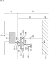
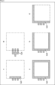
- FIG. 2 shows a schematic plan view of a pixel substrate 41 on which pixels 21 are formed and a control substrate 42 on which control circuits and signal processing circuits for pixels 21 are formed.
- the pixel array section 11 is formed on the pixel substrate 41 at the center of the chip-sized substrate. Furthermore, a plurality of pads 51 are formed on the outer periphery of the substrate outside the pixel array section 11 to serve as contact points with external devices. Each pad 51 of the pixel substrate 41 includes the output section 19 shown in FIG. 1, and is electrically connected to an external device by wire bonding or the like.
- the pads 51 of the pixel substrate 41 include a signal pad 51 to which signals such as pixel signals and control signals are supplied, and a power/ground pad 51 to which a power supply voltage or ground is supplied.
- the shape of the pad 51 is the same for signal use and power supply/ground use.
- the I/F circuit 18 and a plurality of pad wirings 52 are formed on the control board 42.
- the signal processing section 16, the system control section 15, etc. may be formed on the control board 42.
- the pad wiring 52 of the control board 42 is formed at a position corresponding to the pad 51 of the pixel board 41, and is a wiring on the control board 42 side that is electrically connected to the pad 51 located at the same planar position.
- the pad wiring 52 includes a pad wiring 52A (hereinafter referred to as signal pad wiring 52A) electrically connected to the pad 51 for signal use on the pixel substrate 41, and a pad 51 for power supply/ground use on the pixel substrate 41.
- the signal pad wiring 52A and the power/ground pad wiring 52B have different wiring pattern areas, for example.
- FIG. 3 is a cross-sectional view schematically showing the laminated structure of the pixel substrate 41 and the control board 42, and is a cross-sectional view of a portion corresponding to the signal pad wiring 52A.
- the upper pixel substrate 41 and the lower control substrate 42 are bonded together at a bonding surface indicated by a dashed line.
- a light condensing layer 61, a semiconductor substrate 62, and a wiring layer 63 are laminated in order from the top. Therefore, the light condensing layer 61 and the wiring layer 63 are placed on opposite sides of the semiconductor substrate 62 (with the semiconductor substrate 62 as a reference).
- a wiring layer 63 is formed on the front side of the semiconductor substrate 62, and a light collecting layer 61 is formed on the back side.
- An on-chip microlens 67, a color filter 68, etc. are formed on the light collecting layer 61.
- Light from the object that has entered the upper surface (incident surface) of the light collecting layer 61 is focused by an on-chip microlens 67 onto a photodiode (not shown) formed on the semiconductor substrate 62.
- the semiconductor substrate 62 is formed using, for example, a silicon substrate using silicon (Si) as a semiconductor.
- the material of the semiconductor substrate 62 may be, for example, a group IV semiconductor such as Ge, or a group III-V semiconductor such as GaAs, InP, or InGaAs.
- semiconductor elements such as a photodiode, a transfer gate, a charge-voltage conversion section (FD section), a reset gate, an amplification transistor, and a selection transistor of each pixel 21 are formed on the semiconductor substrate 62. ing.
- a plurality of layers of wiring 64 and an interlayer insulating film 65 are formed in the wiring layer 63.
- the wiring 64 in each layer is connected to the wiring 64 in the upper or lower layer through vias 66 in required areas.
- the wiring 64 and the via 66 are made of, for example, a metal material such as Cu or Al.
- pads 51 for external connection are formed in the wiring layer 63.
- the pad 51 is formed to have approximately the same height and thickness as the wiring 64 in the second to fourth layers of the wiring layer 63.
- a through hole 71 is formed above the pad 51 and penetrates the light collecting layer 61 and the semiconductor substrate 62 . Through this through hole 71, a part of the surface of the pad 51 on which the wire bond ball is formed (hereinafter referred to as a connection surface) is exposed.
- a via 73 is connected to the surface of the pad 51 opposite to the connection surface, and the pad 51 is connected to a pad 72 for bonding to the control board 42 via the via 73.
- the pad 72 is made of, for example, Cu.
- the pad 72 is connected to the pad 91 of the wiring layer 81 of the control board 42 by Cu--Cu bonding.
- a wiring layer 81 and a semiconductor substrate 82 are laminated in order from the top.
- the wiring layer 81 of the control board 42 is formed on the wiring layer 63 side of the pixel board 41, and the wiring layer 63 of the pixel board 41 and the wiring layer 81 of the control board 42 are in contact with each other.
- a plurality of layers of wiring 83 and an interlayer insulating film 84 are formed in the wiring layer 81.
- the wiring 83 in each layer is connected to the wiring 83 in the upper or lower layer by vias 85 in required areas.
- the wiring 83 and the via 85 are made of, for example, a metal material such as Cu or Al.
- a pad 91 for bonding to the pixel substrate 41 is formed at the upper end of the wiring layer 81.
- Pad 91 is made of, for example, Cu. Although a gap is left in FIG. 3 for clarity, the lower surface of the pad 72 of the pixel substrate 41 and the upper surface of the pad 91 of the control board 42 are connected by Cu--Cu bonding.
- a pad 91 on the control board 42 which is Cu-Cu bonded to a pad 72 on the pixel board 41 is connected to the signal pad wiring 52A in the uppermost layer in the wiring layer 81 via a via 92.
- a wiring 83A is provided at a predetermined position on the same layer as the signal pad wiring 52A, and the wiring 83A is connected to a lower layer wiring 83B via a via 85A.
- the semiconductor substrate 82 is formed of, for example, a silicon substrate, but similarly to the semiconductor substrate 62 described above, a material other than silicon may be used.
- the solid-state imaging device 1 in which the pixel substrate 41 and the control board 42 are stacked as described above is a back-illuminated MOS solid-state imaging device in which light enters from the back side of the semiconductor substrate 62.
- the pad 51 on the pixel board 41 side that outputs a pixel signal as an output signal is connected to the signal pad wiring 52A on the control board 42 side via the via 73, the pad 72, the pad 91, and the via 92. electrically connected.
- the signal pad wiring 52A, wiring 83A, wiring 83B, etc. have a structure that suppresses the influence of capacitance due to electrical characteristics, thereby increasing the speed of the communication interface. and wideband.
- the wiring structure within the wiring layer 81 on the control board 42 side that realizes high-speed and wide-band communication interface will be described in detail below.
- FIG. 4 is a cross-sectional view showing details of the pad wiring structure in the wiring layer 81 on the control board 42 side connected to the signal pad 51 of the pixel board 41 in FIG.
- the pad 51 of the pixel board 41 is connected to the signal pad wiring 52A of the control board 42 via the via 73, the pad 72, the pad 91, and the via 92.
- the output signal SIG is supplied to the signal pad wiring 52A, and the output signal SIG is output from the pad 51 of the pixel substrate 41 to an external device via the pad 91, the pad 72, etc.
- the wiring 83A formed in the same layer as the signal pad wiring 52A is connected to the lower layer wiring 83B via the via 85A, and the lower layer wiring 83B is connected to the high resistance element 101 in the wiring layer 81 via the via 85B etc. , and is connected to the wiring 83C.
- a VSS potential (eg, GND) is supplied to the wiring 83C.
- the VSS potential is also supplied to the wirings 83A and 83B via the high resistance element 101, and the wirings 83A and 83B constitute shield wiring.
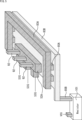
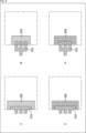
- FIG. 5 is a perspective view showing a specific example of the arrangement of a signal pad wiring 52A to which the output signal SIG is input, and wirings 83A and 83B formed as shield wirings around the signal pad wiring 52A. Note that in FIG. 5, the patterns of the wirings 83A, 83B, etc. are shown different from those in FIG. 4 in order to make the diagram easier to understand.
- the signal pad wiring 52A to which the output signal SIG is input is formed with a smaller planar area than the pad 51 of the pixel substrate 41 within a range that allows the current value of the output signal SIG.
- the signal pad wiring 52A is formed in the shape of three comb teeth, and three vias 92 are also formed for connection to the upper layer pad 91 (FIG. 4).
- the area may be formed in accordance with the current value of the output signal SIG, and is not limited to this example.
- the wiring 83A is arranged in the same layer as the signal pad wiring 52A so as to surround the signal pad wiring 52A, and the wiring 83B is formed at a position overlapping the signal pad wiring 52A and the wiring 83A in plan view.
- Wiring 83B is connected to high resistance element 101 via one or more vias (including via 85B).
- the pad 51 of the pixel substrate 41 in FIG. 4 is formed with a thickness and area that can withstand the stress of the wire bond ball. Since the pad 51 of the pixel board 41 has sufficient stress resistance, the signal pad wiring 52A on the control board 42 side connected to the pad 51 only needs to have current resistance for the output signal SIG. It can be formed with the minimum planar area that allows the current value.
- Capacitances 102A and 102B which are pad coupling capacitances, occur between the signal pad wiring 52A and the adjacent wirings 83A and 83B in the same layer or lower layer, but by forming the signal pad wiring 52A with the minimum area, the pad The coupling capacitance can be reduced. Further, by feeding the VSS potential to the wirings 83A and 83B via the high resistance element 101, the shield capacitance (capacitances 102A and 102B) can be nullified.
- a parasitic capacitance 103 that occurs between the upper and lower wirings 83 occurs between the wiring 83B and the well region 111 (or P sub-substrate region) of the semiconductor substrate 82, but this parasitic capacitance 103 also has a high It can be nullified by supplying the VSS potential through the resistance element 101.
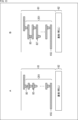
- a in FIG. 6 is an RC circuit (hereinafter referred to as the present RC circuit) corresponding to the present method of feeding the VSS potential to the shield wiring via the high-resistance element 101, and B in FIG.
- This is an RC circuit as a comparative example (hereinafter referred to as a comparative RC circuit) without the high resistance element 101 or shield wiring.
- the resistor 151 is the wiring resistance of the signal pad wiring 52A, etc.
- the capacitor 152 is the capacitance 102A and 102B of the shield wiring (wirings 83A and 83B)
- the resistor 153 is the high resistance Corresponds to element 101.
- Resistor 155 is a terminating resistor.
- the voltage waveform V M1 at the output end 154 in this RC circuit can be expressed as in the equation shown in FIG.
- a resistor 151' is a wiring resistance such as the signal pad wiring 52A, and a capacitor 152' corresponds to the parasitic capacitance 103 generated between the signal pad wiring 52A and the wiring 83.
- Resistor 155 is a terminating resistor.
- the voltage waveform V M2 at the output terminal 154 in the comparison RC circuit can be expressed as in the equation shown in FIG.
- the conditions of this RC circuit and the comparative RC circuit are the same except for the resistor 153 corresponding to the high resistance element 101.
- the resistance value R 0 of the resistor 151 is 50 ⁇
- the capacitance C of the capacitors 152 and 152' is 1.0 pF
- the resistance value R L of the resistor 155 which is the terminating resistor, is 50 ⁇ .
- the resistance value Rp of the resistor 153 is 500 ⁇ .
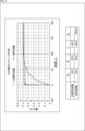
- FIG. 7 shows the signal waveforms output from the output terminals 154 of each of the present RC circuit and the comparative RC circuit.
- the transition time is significantly shortened compared to the comparative RC circuit.
- the effective capacitance component can be made to appear small like a low-pass filter in the frequency band where high-speed interface communication is performed. This makes it possible to increase the data rate and realize a faster communication interface.
- the resistance value Rp of the high-resistance element 101 corresponding to the resistor 153 is appropriately set according to the communication frequency of the high-speed interface.
- the signal pad wiring 52A on the control board 42 side does not need to have a uniform pattern shape as long as the current value of the output signal SIG is allowed, and can be formed in a planar shape suitable for each application. .
- the wiring pattern (planar shape) of the signal pad wiring 52A may be determined according to the impedance allowed for connection with the signal pad 51 of the pixel substrate 41, etc.
- a to E in FIG. 8 show examples of wiring patterns of the signal pad wiring 52A.
- a rectangle indicated by a dashed dotted line indicates a formation area of the pad 51 on the pixel substrate 41 side that is connected to the signal pad wiring 52A.
- FIG. 8A is a plan view of the wiring pattern of the signal pad wiring 52A shown in FIG. 5.
- the signal pad wiring 52A is composed of three comb-shaped patterns and one linear pattern connected perpendicularly to the three comb-shaped patterns.
- FIG. 8B is a plan view showing another example of the wiring pattern of the signal pad wiring 52A.
- the signal pad wiring 52A shown in FIG. 8B is composed of three comb-shaped patterns.
- FIG. 8C is a plan view showing another example of the wiring pattern of the signal pad wiring 52A.
- the signal pad wiring 52A in FIG. 8C is composed of three linear patterns and a rectangular pattern with a predetermined line width formed along the outer periphery of the rectangular pad 51 on the pixel substrate 41 side. Ru.
- FIG. 8D is a plan view showing another example of the wiring pattern of the signal pad wiring 52A.
- the signal pad wiring 52A shown in D in FIG. 8 includes three linear patterns and a U-shaped pattern with a predetermined line width formed along three sides of the rectangular pad 51 on the pixel substrate 41 side. configured.
- FIG. 8E is a plan view showing another wiring pattern example of the signal pad wiring 52A.
- the signal pad wiring 52A shown in E of FIG. 8 includes three linear patterns and an L-shaped pattern with a predetermined line width formed along two sides of the rectangular pad 51 on the pixel substrate 41 side. configured.
- the wiring pattern of the signal pad wiring 52A may have a pattern shape other than the examples shown in FIGS. 8A to 8E.
- FIGS. 9A to 9D show examples of the wiring pattern of the wiring 83B arranged under the signal pad wiring 52A to which the output signal SIG is input.
- the wiring pattern of the signal pad wiring 52A is also shown superimposed, and the wiring pattern of A or B of FIG. 8 is adopted as the wiring pattern of the signal pad wiring 52A.
- a rectangle indicated by a chain line indicates a formation area of the pad 51 on the pixel substrate 41 side.
- the wiring pattern of the wiring 83B arranged under the signal pad wiring 52A may be a solid film pattern as shown in A and B of FIG. 9, or a mesh pattern (lattice pattern) as shown in C and D of FIG. ) etc.
- the pattern area of the wiring 83B is different between A and B in FIG. Similarly, in C and D in FIG. 9, the pattern area of the wiring 83B is different.
- the wiring pattern of the wiring 83B that determines the potential of the capacitor 102B is appropriately determined according to the communication frequency of the output signal SIG.
- FIGS. 10A and 10B show an example of a wiring pattern of a wiring 83A arranged in the same layer as the signal pad wiring 52A to which the output signal SIG is input.
- 10A and 10B also show the wiring patterns of the signal pad wiring 52A and the lower layer wiring 83B.
- the wiring pattern shown in FIG. 9A is used as the wiring pattern of the signal pad wiring 52A and the wiring 83B, but it goes without saying that other wiring patterns may be used.
- a rectangle indicated by a chain line indicates a region where the pad 51 is formed on the pixel substrate 41 side.
- the wiring pattern of the wiring 83A is a U-shaped pattern as shown in A in FIG. 10, which surrounds the signal pad wiring 52A to which the output signal SIG is input in three directions, horizontally and vertically. be able to.
- an I-shaped (linear) pattern shape as shown in FIG. 10B may be used.
- the wiring pattern of the wiring 83A that determines the potential of the capacitor 102A is appropriately determined according to the communication frequency of the output signal SIG.
- FIG. 8 shows an example of the wiring pattern of the signal pad wiring 52A
- FIG. 9 shows an example of the wiring pattern of the wiring 83B in the same layer as the signal pad wiring 52A
- FIG. An example of a wiring pattern is shown.
- the combination of the wiring patterns of the signal pad wiring 52A, the wiring 83A, and the wiring 83B can be arbitrarily selected, and pattern shapes other than those illustrated may be adopted.
- both the wiring 83A and the wiring 83B as shield wiring are arranged around the signal pad wiring 52A to which the output signal SIG is input, but the wiring 83A on the same layer as the signal pad wiring 52A is Alternatively, only one of the lower layer wirings 83B may be provided.
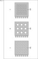
- the pad wiring 52 connected to the pad 51 of the pixel substrate 41 includes a power/ground pad wiring 52B in addition to the signal pad wiring 52A.
- FIG. 11 show examples of wiring patterns of the power supply/ground pad wiring 52B.
- rectangles indicated by one-dot chain lines (which overlap in many parts) indicate the formation area of the pad 51 on the pixel substrate 41 side.
- the power supply/ground pad wiring 52B is required to flow a sufficient current, so it is formed to have a high pattern density so as to have low impedance.
- the power/ground pad wiring 52B is formed in a rectangular pattern having the same size as the pad 51 on the pixel substrate 41 side, as shown in FIG. 11A.
- the power supply/ground pad wiring 52B may be a mesh pattern with a thick line width as shown in B of FIG. 11, or a mesh pattern with a thin line width but many lines as shown in C of FIG. 11. may be formed. Pattern shapes other than the wiring patterns illustrated in FIGS. 11A to 11C may also be employed.
- the wiring pattern of the power supply/ground pad wiring 52B is formed with a larger planar area and pattern density than the signal pad wiring 52A for signal use.
- the high resistance element 101 can be composed of a parasitic resistance due to a stacked via 201 formed in the wiring layer 81 and a metal resistance 202.
- the stacked via 201 is composed of multiple layers of wiring 83 and vias 85 that connect the upper and lower wirings 83, and the number of stacked wirings 83 and the number of vias 85 can be determined as appropriate.
- the metal resistor 202 may be replaced with a polysilicon resistor using polysilicon.
- the high-resistance element 101 is composed of a parasitic resistance caused by a stacked via 201 formed in a wiring layer 81 and a diffused resistance 203 formed by a diffusion layer of a semiconductor substrate 82. be able to.
- the high resistance element 101 may be configured only with parasitic resistance due to stacked vias 201 formed in the wiring layer 81, as shown in FIG. 13A.
- the high resistance element 101 may be configured with a parasitic resistance formed by a combination of a thin wiring 83' and a stacked via 201.
- the high resistance element 101 can be realized in a small area.
- VSS potential for example, GND
- GND GND
- the potential supplied to the wirings 83A and 83B via the high resistance element 101 may be different from the VSS potential. More specifically, a Vcom potential higher than the VSS potential (Vcom>VSS) can be supplied to the wirings 83A and 83B via the high resistance element 101.
- FIG. 14 shows the signal pad wiring 52A and the I/F circuit 18 that outputs the output signal SIG when the VSS potential is supplied to the wirings 83A and 83B as shield wirings. Note that the output signal SIG is a differential signal.
- the Vouth potential generated by the regulator 251 and the VSS potential are supplied to the driver 252.
- the driver 252 generates an output signal SIG, which is a differential signal in which the VSS potential is an OFF potential and the Vouth potential is an ON potential, and outputs each to the signal pad wiring 52A.
- SIG an output signal in which the VSS potential is an OFF potential and the Vouth potential is an ON potential
- FIG. 15 shows the signal pad wiring 52A and the I/F circuit 18 that outputs the output signal SIG when the Vcom potential is supplied to the wirings 83A and 83B as shield wirings.
- the capacitance 102 that is the pad coupling capacitance will be lower than the Vcom potential. Since the noise is separated from the noise of the semiconductor substrate 82, the noise is not superimposed on the output signal SIG and causes jitter.
- FIG. 16 shows the signal pad wiring 52A and the I/F that outputs the output signal SIG when the ON and OFF potentials of the output signal SIG are generated based on the Vcom potential instead of the VSS potential. Circuit 18 is shown.
- the regulator 251H In the I/F circuit 18, the regulator 251H generates a Vouth potential that is an ON potential and supplies it to the driver 252.
- the regulator 251L generates a Voutl potential, which is an OFF potential, and supplies it to the driver 252.
- the driver 252 generates an output signal SIG, which is a differential signal in which the Voutl potential is an OFF potential and the Vouth potential is an ON potential, and outputs each to the signal pad wiring 52A. If noise is included in the well at the VSS potential of the semiconductor substrate 82, the noise will not be in the same phase as fluctuations in the output signal SIG, and will therefore be superimposed on the output signal SIG as jitter.
- FIG. 17 shows the signal pad wiring 52A and the signal pad wiring 52A when generating the ON potential and OFF potential of the output signal SIG based on the Vcom potential and supplying the Vcom potential to the wirings 83A and 83B as shield wirings, and outputting the output signal SIG.
- An I/F circuit 18 is shown.
- the output signal SIG is generated based on the Vcom potential and the Vcom potential is supplied to the wirings 83A and 83B as shield wirings, even if the well at the VSS potential of the semiconductor substrate 82 contains noise, Since the capacitor 102, which is a pad coupling capacitor, is coupled to the Vcom potential, it is separated from the noise of the semiconductor substrate 82, and the noise is not superimposed on the output signal SIG to cause jitter.
- the VSS potential (for example, GND) may be supplied to the wirings 83A and 83B as shield wirings via the high resistance element 101, but the Vcom potential (Vcom>VSS ), it is possible to prevent VSS noise from being superimposed on the output signal SIG.
- the signal pad wiring 52A With a planar area as small as possible to allow the current value of the output signal SIG, the space of the wiring layer 81 is freed, and the degree of freedom of the wiring 83 is improved. Utilizing this, by supplying a Vcom potential different from the VSS potential to the wirings 83A and 83B as shield wirings, it is possible to reduce the charging and discharging charges of the pad coupling capacitance.
- FIG. 18 is a diagram showing an example of use of an image sensor using the solid-state imaging device 1 described above.
- the solid-state imaging device 1 described above can be used as an image sensor in various cases for sensing light such as visible light, infrared light, ultraviolet light, and X-rays, for example, as described below.
- ⁇ Digital cameras, mobile devices with camera functions, and other devices that take images for viewing purposes Devices used for transportation, such as in-vehicle sensors that take pictures of the rear, surroundings, and interior of the car, surveillance cameras that monitor moving vehicles and roads, and distance sensors that measure the distance between vehicles, etc.
- Devices used for transportation such as in-vehicle sensors that take pictures of the rear, surroundings, and interior of the car, surveillance cameras that monitor moving vehicles and roads, and distance sensors that measure the distance between vehicles, etc.
- User gestures Devices used in home appliances such as TVs, refrigerators, and air conditioners to take pictures and operate devices according to the gestures.
- - Endoscopes devices that perform blood vessel imaging by receiving infrared light, etc.
- Devices used for medical and healthcare purposes - Devices used for security, such as surveillance cameras for crime prevention and cameras for person authentication - Skin measurement devices that take pictures of the skin, and devices that take pictures of the scalp - Devices used for beauty purposes, such as microscopes for skin care.
- - Devices used for sports such as action cameras and wearable cameras.
- - Cameras, etc. used to monitor the condition of fields and crops. , equipment used for agricultural purposes
- the technology of the present disclosure is not limited to application to solid-state imaging devices. That is, the technology of the present disclosure applies to an image capture unit (photoelectric conversion unit) in an image capture device such as a digital still camera or a video camera, a mobile terminal device having an image capture function, or a copying machine that uses a solid-state image capture device in an image reading unit. ) is applicable to all electronic devices that use solid-state imaging devices.
- the solid-state imaging device may be formed as a single chip, or may be a module having an imaging function in which an imaging section and a signal processing section or an optical system are packaged together.
- FIG. 19 is a block diagram showing a configuration example of an imaging device as an electronic device to which the technology of the present disclosure is applied.
- the imaging device 300 in FIG. 19 includes an optical section 301 including a lens group, a solid-state imaging device (imaging device) 302 in which the configuration of the solid-state imaging device 1 in FIG. 1 is adopted, and a DSP (Digital Signal (processor) circuit 303.
- the imaging device 300 also includes a frame memory 304, a display section 305, a recording section 306, an operation section 307, and a power supply section 308.
- the DSP circuit 303, frame memory 304, display section 305, recording section 306, operation section 307, and power supply section 308 are interconnected via a bus line 309.
- the optical section 301 takes in incident light (image light) from a subject and forms an image on the imaging surface of the solid-state imaging device 302.
- the solid-state imaging device 302 converts the amount of incident light that is imaged on the imaging surface by the optical section 301 into an electrical signal for each pixel, and outputs the electric signal as a pixel signal.
- a shield wiring (wiring 83A or 83B) is arranged around the signal pad wiring 52A of the solid-state imaging device 1 of FIG. 1, that is, the control board 42 side to which the output signal SIG is supplied, and a high resistance
- a solid-state imaging device in which a predetermined potential (VSS potential or Vcom potential) is supplied via the element 101 can be used.
- the display unit 305 is configured with a thin display such as an LCD (Liquid Crystal Display) or an organic EL (Electro Luminescence) display, and displays moving images or still images captured by the solid-state imaging device 302.
- the recording unit 306 records a moving image or a still image captured by the solid-state imaging device 302 on a recording medium such as a hard disk or a semiconductor memory.
- the operation unit 307 issues operation commands regarding various functions of the imaging device 300 under operation by the user.
- the power supply section 308 appropriately supplies various kinds of power to serve as operating power for the DSP circuit 303, frame memory 304, display section 305, recording section 306, and operation section 307 to these supply targets.
- the solid-state imaging device 302 As described above, by employing the configuration of the solid-state imaging device 1 described above as the solid-state imaging device 302, it is possible to realize a faster communication interface. Therefore, it is possible to increase the speed of captured images even in the imaging device 300 such as a video camera, a digital still camera, or a camera module for mobile devices such as a mobile phone.
- the imaging device 300 such as a video camera, a digital still camera, or a camera module for mobile devices such as a mobile phone.
- the technology according to the present disclosure (this technology) can be applied to various products.
- the technology according to the present disclosure may be realized as a device mounted on any type of moving body such as a car, electric vehicle, hybrid electric vehicle, motorcycle, bicycle, personal mobility, airplane, drone, ship, robot, etc. It's okay.
- FIG. 20 is a block diagram illustrating a schematic configuration example of a vehicle control system, which is an example of a mobile body control system to which the technology according to the present disclosure can be applied.
- the vehicle control system 12000 includes a plurality of electronic control units connected via a communication network 12001.
- the vehicle control system 12000 includes a drive system control unit 12010, a body system control unit 12020, an outside vehicle information detection unit 12030, an inside vehicle information detection unit 12040, and an integrated control unit 12050.
- a microcomputer 12051, an audio/image output section 12052, and an in-vehicle network I/F (interface) 12053 are illustrated.
- the drive system control unit 12010 controls the operation of devices related to the drive system of the vehicle according to various programs.
- the drive system control unit 12010 includes a drive force generation device such as an internal combustion engine or a drive motor that generates drive force for the vehicle, a drive force transmission mechanism that transmits the drive force to wheels, and a drive force transmission mechanism that controls the steering angle of the vehicle. It functions as a control device for a steering mechanism to adjust and a braking device to generate braking force for the vehicle.
- the body system control unit 12020 controls the operations of various devices installed in the vehicle body according to various programs.
- the body system control unit 12020 functions as a keyless entry system, a smart key system, a power window device, or a control device for various lamps such as a headlamp, a back lamp, a brake lamp, a turn signal, or a fog lamp.
- radio waves transmitted from a portable device that replaces a key or signals from various switches may be input to the body control unit 12020.
- the body system control unit 12020 receives input of these radio waves or signals, and controls the door lock device, power window device, lamp, etc. of the vehicle.
- the external information detection unit 12030 detects information external to the vehicle in which the vehicle control system 12000 is mounted.
- an imaging section 12031 is connected to the outside-vehicle information detection unit 12030.
- the vehicle exterior information detection unit 12030 causes the imaging unit 12031 to capture an image of the exterior of the vehicle, and receives the captured image.
- the external information detection unit 12030 may perform object detection processing such as a person, car, obstacle, sign, or text on the road surface or distance detection processing based on the received image.
- the imaging unit 12031 is an optical sensor that receives light and outputs an electrical signal according to the amount of received light.
- the imaging unit 12031 can output the electrical signal as an image or as distance measurement information.
- the light received by the imaging unit 12031 may be visible light or non-visible light such as infrared rays.
- the in-vehicle information detection unit 12040 detects in-vehicle information.
- a driver condition detection section 12041 that detects the condition of the driver is connected to the in-vehicle information detection unit 12040.
- the driver condition detection unit 12041 includes, for example, a camera that images the driver, and the in-vehicle information detection unit 12040 detects the degree of fatigue or concentration of the driver based on the detection information input from the driver condition detection unit 12041. It may be calculated, or it may be determined whether the driver is falling asleep.
- the microcomputer 12051 calculates control target values for the driving force generation device, steering mechanism, or braking device based on the information inside and outside the vehicle acquired by the vehicle exterior information detection unit 12030 or the vehicle interior information detection unit 12040, Control commands can be output to 12010.
- the microcomputer 12051 realizes ADAS (Advanced Driver Assistance System) functions, including vehicle collision avoidance or impact mitigation, following distance based on vehicle distance, vehicle speed maintenance, vehicle collision warning, vehicle lane departure warning, etc. It is possible to perform cooperative control for the purpose of ADAS (Advanced Driver Assistance System) functions, including vehicle collision avoidance or impact mitigation, following distance based on vehicle distance, vehicle speed maintenance, vehicle collision warning, vehicle lane departure warning, etc. It is possible to perform cooperative control for the purpose of
- ADAS Advanced Driver Assistance System
- the microcomputer 12051 controls the driving force generating device, steering mechanism, braking device, etc. based on information about the surroundings of the vehicle acquired by the vehicle exterior information detection unit 12030 or the vehicle interior information detection unit 12040. It is possible to perform cooperative control for the purpose of autonomous driving, etc., which does not rely on operation.
- the microcomputer 12051 can output a control command to the body system control unit 12020 based on the information outside the vehicle acquired by the outside information detection unit 12030.
- the microcomputer 12051 controls the headlamps according to the position of the preceding vehicle or oncoming vehicle detected by the vehicle exterior information detection unit 12030, and performs cooperative control for the purpose of preventing glare, such as switching from high beam to low beam. It can be carried out.
- the audio and image output unit 12052 transmits an output signal of at least one of audio and images to an output device that can visually or audibly notify information to the occupants of the vehicle or to the outside of the vehicle.
- an audio speaker 12061, a display section 12062, and an instrument panel 12063 are illustrated as output devices.
- the display unit 12062 may include, for example, at least one of an on-board display and a head-up display.
- FIG. 21 is a diagram showing an example of the installation position of the imaging section 12031.
- the vehicle 12100 has imaging units 12101, 12102, 12103, 12104, and 12105 as the imaging unit 12031.
- the imaging units 12101, 12102, 12103, 12104, and 12105 are provided, for example, at positions such as the front nose, side mirrors, rear bumper, back door, and the top of the windshield inside the vehicle 12100.
- An imaging unit 12101 provided in the front nose and an imaging unit 12105 provided above the windshield inside the vehicle mainly acquire images in front of the vehicle 12100.
- Imaging units 12102 and 12103 provided in the side mirrors mainly capture images of the sides of the vehicle 12100.
- An imaging unit 12104 provided in the rear bumper or back door mainly captures images of the rear of the vehicle 12100.
- the images of the front acquired by the imaging units 12101 and 12105 are mainly used for detecting preceding vehicles, pedestrians, obstacles, traffic lights, traffic signs, lanes, and the like.
- FIG. 21 shows an example of the imaging range of the imaging units 12101 to 12104.
- An imaging range 12111 indicates the imaging range of the imaging unit 12101 provided on the front nose
- imaging ranges 12112 and 12113 indicate imaging ranges of the imaging units 12102 and 12103 provided on the side mirrors, respectively
- an imaging range 12114 shows the imaging range of the imaging unit 12101 provided on the front nose.
- the imaging range of the imaging unit 12104 provided in the rear bumper or back door is shown. For example, by overlapping the image data captured by the imaging units 12101 to 12104, an overhead image of the vehicle 12100 viewed from above can be obtained.
- At least one of the imaging units 12101 to 12104 may have a function of acquiring distance information.
- at least one of the imaging units 12101 to 12104 may be a stereo camera including a plurality of image sensors, or may be an image sensor having pixels for phase difference detection.
- the microcomputer 12051 determines the distance to each three-dimensional object within the imaging ranges 12111 to 12114 and the temporal change in this distance (relative speed with respect to the vehicle 12100) based on the distance information obtained from the imaging units 12101 to 12104. In particular, by determining the three-dimensional object that is closest to the vehicle 12100 on its path and that is traveling at a predetermined speed (for example, 0 km/h or more) in approximately the same direction as the vehicle 12100, it is possible to extract the three-dimensional object as the preceding vehicle. can.
- a predetermined speed for example, 0 km/h or more
- the microcomputer 12051 can set an inter-vehicle distance to be secured in advance in front of the preceding vehicle, and perform automatic brake control (including follow-up stop control), automatic acceleration control (including follow-up start control), and the like. In this way, it is possible to perform cooperative control for the purpose of autonomous driving, etc., in which the vehicle travels autonomously without depending on the driver's operation.
- the microcomputer 12051 transfers three-dimensional object data to other three-dimensional objects such as two-wheeled vehicles, regular vehicles, large vehicles, pedestrians, and utility poles based on the distance information obtained from the imaging units 12101 to 12104. It can be classified and extracted and used for automatic obstacle avoidance. For example, the microcomputer 12051 identifies obstacles around the vehicle 12100 into obstacles that are visible to the driver of the vehicle 12100 and obstacles that are difficult to see. Then, the microcomputer 12051 determines a collision risk indicating the degree of risk of collision with each obstacle, and when the collision risk exceeds a set value and there is a possibility of a collision, the microcomputer 12051 transmits information via the audio speaker 12061 and the display unit 12062. By outputting a warning to the driver via the vehicle control unit 12010 and performing forced deceleration and avoidance steering via the drive system control unit 12010, driving support for collision avoidance can be provided.
- the microcomputer 12051 determines a collision risk indicating the degree of risk of collision with each obstacle, and when the collision risk exceed
- At least one of the imaging units 12101 to 12104 may be an infrared camera that detects infrared rays.
- the microcomputer 12051 can recognize a pedestrian by determining whether the pedestrian is present in the images captured by the imaging units 12101 to 12104.
- pedestrian recognition involves, for example, a procedure for extracting feature points in images captured by the imaging units 12101 to 12104 as infrared cameras, and a pattern matching process is performed on a series of feature points indicating the outline of an object to determine whether it is a pedestrian or not.
- the audio image output unit 12052 creates a rectangular outline for emphasis on the recognized pedestrian.
- the display unit 12062 is controlled to display the .
- the audio image output unit 12052 may control the display unit 12062 to display an icon or the like indicating a pedestrian at a desired position.
- the technology according to the present disclosure can be applied to the imaging unit 12031 among the configurations described above.
- the solid-state imaging device 1 described above can be applied as the imaging section 12031.
- the present disclosure is not limited to application to a solid-state imaging device that detects the distribution of the incident amount of visible light and captures the image as an image, but also applies to a solid-state imaging device that captures the distribution of the incident amount of infrared rays, X-rays, particles, etc. as an image. It can be applied to all solid-state imaging devices (physical quantity distribution detection devices) such as imaging devices and, in a broader sense, fingerprint detection sensors that detect the distribution of other physical quantities such as pressure and capacitance and capture the images as images. be.
- the technology of the present disclosure is applicable not only to solid-state imaging devices but also to all semiconductor devices having other semiconductor integrated circuits.
- the technology of the present disclosure can take the following configuration.
- (1) It is constructed by laminating a pixel substrate on which pixels are formed and a control board,
- the pixel substrate has a pad that serves as a contact point with an external device,
- the control board is a signal pad wiring connected to the pad; a shield wiring arranged around the signal pad wiring;
- a solid-state imaging device comprising: a high resistance element connected to the shield wiring.
- the solid-state imaging device according to any one of (1) to (4), wherein the shield wiring is arranged in at least one of the same layer or a lower layer as the signal pad wiring.
- the high-resistance element includes a metal resistor or a polysilicon resistor.
- the high-resistance element includes a diffused resistor.
- the high resistance element includes a well resistance.
- the solid-state imaging device according to any one of (1) to (8), wherein the high-resistance element includes a parasitic resistance due to a stacked via.
- the solid-state imaging device according to any one of (1) to (8), wherein the high-resistance element includes a parasitic resistance due to stacked vias and thin wiring.
- the signal pad wiring has a smaller planar area than the pad.
- the pad includes a first pad that outputs a pixel signal of the pixel and a second pad that is supplied with a power supply voltage or ground.
- It is constructed by laminating a pixel substrate on which pixels are formed and a control board, The pixel substrate has a pad that serves as a contact point with an external device, The control board is a signal pad wiring connected to the pad; a shield wiring arranged around the signal pad wiring;
- An electronic device comprising: a solid-state imaging device comprising: a high resistance element connected to the shield wiring;
- Solid-state imaging device 18 I/F circuit, 21 pixels, 41 pixel board, 42 control board, 51 pad, 52 pad wiring, 52A pad wiring, 52B pad wiring, 62 semiconductor substrate, 71 penetration Hole, 72 pad, 73 via , 81 wiring layer, 82 semiconductor substrate, 83, 83A, 83B, 83C wiring, 84 interlayer insulating film, 85, 85A, 85B via, 101 high resistance element, 102, 102A, 102B capacitor, 103 Raw capacity, 111 well area, 201 Stacked via, 202 Metal resistance, 203 Diffused resistance, 204 P well, 207 P well resistance, 211 N well, 214 N well resistance, 251 Regulator, 251H Regulator, 251L Regulator, 252 driver, 300 imaging device, 302 solid-state imaging device
Abstract
This disclosure relates to a solid-state imaging device and an electronic apparatus with which it is possible to achieve increased speed for a communication interface. This solid-state imaging device is configured by layering a control substrate and a pixel substrate on which pixels are formed. The pixel substrate has a pad that serves as a contact with an external device. The control substrate has: signal pad wiring connected to the pad; a shield wiring line disposed in the periphery of the signal pad wiring line; and a high resistance element connected to the shield wiring line. This disclosure can, for example, be applied to a solid-state imaging device or the like.
Description
本開示は、固体撮像装置および電子機器に関し、特に、通信インターフェースの高速化を実現できるようにした固体撮像装置および電子機器に関する。
The present disclosure relates to a solid-state imaging device and an electronic device, and particularly relates to a solid-state imaging device and an electronic device that can realize high-speed communication interfaces.
画素が形成された画素基板と、画素の制御等を行う制御回路が形成された制御基板とを積層した積層構造の裏面照射型の固体撮像装置が普及してきている。積層構造を有する裏面照射型の固体撮像装置において、画素信号等を出力する出力部としてのパッドを制御基板側に形成し、画素基板側ではパッド部上を開口処理した構造がある。このような構造は画素基板側からみてパッド位置が深くなるため、パッド上に形成するワイヤボンディングの精度が必要となり、アッセンブリ品質の低下の原因となる。
Back-illuminated solid-state imaging devices with a stacked structure in which a pixel substrate on which pixels are formed and a control board on which a control circuit for controlling the pixels and the like are stacked are becoming popular. BACKGROUND ART In a back-illuminated solid-state imaging device having a stacked structure, there is a structure in which a pad serving as an output section for outputting pixel signals and the like is formed on the control board side, and an opening is formed on the pad section on the pixel board side. In such a structure, since the pad position is deep when viewed from the pixel substrate side, precision in wire bonding formed on the pad is required, which causes deterioration in assembly quality.
そこで、特許文献1では、画素基板の最上層の配線層にパッドを形成した構造が提案されている。また、特許文献2には、画素基板の最上層の配線層にパッドを形成した場合に、画素基板のパッドを制御基板側の配線と接続し、カラーフィルタ、マイクロレンズ等の形成、熱処理時のデバイス特性変動などの品質を改善する技術が提案されている。
Therefore, Patent Document 1 proposes a structure in which pads are formed in the uppermost wiring layer of the pixel substrate. Furthermore, Patent Document 2 discloses that when a pad is formed on the uppermost wiring layer of a pixel substrate, the pad of the pixel substrate is connected to the wiring on the control board side, and the pad is connected to the wiring layer on the control board side to form color filters, microlenses, etc., and during heat treatment. Techniques have been proposed to improve quality such as device characteristic fluctuations.
しかしながら、画素基板のパッドを制御基板側の配線と接続した場合、パッド容量が大きくなってしまうことが懸念される。固体撮像装置に対する画素数増、動画性能への要求の高まりから、固体撮像装置に実装されている通信インターフェースのボーレートは年々高速化しており、パッド容量は高速化を律束する要因の一つとなっている。
However, if the pad of the pixel substrate is connected to the wiring on the control board side, there is a concern that the pad capacitance will increase. The baud rate of the communication interface installed in solid-state imaging devices is increasing year by year due to the increase in the number of pixels in solid-state imaging devices and the growing demand for video performance, and pad capacity is one of the factors that determines the speed increase. ing.
本開示は、このような状況に鑑みてなされたものであり、通信インターフェースの高速化を実現できるようにするものである。
The present disclosure has been made in view of this situation, and is intended to make it possible to realize faster communication interfaces.
本開示の第1の側面の固体撮像装置は、画素が形成された画素基板と、制御基板とを積層して構成され、前記画素基板は、外部装置との接点となるパッドを有し、前記制御基板は、前記パッドと接続された信号パッド配線と、前記信号パッド配線の周辺に配置されたシールド配線と、前記シールド配線と接続された高抵抗素子とを有する。
A solid-state imaging device according to a first aspect of the present disclosure is configured by laminating a pixel substrate on which pixels are formed and a control board, the pixel substrate having a pad that serves as a contact point with an external device, and the pixel substrate having a pad that serves as a contact point with an external device, The control board includes a signal pad wiring connected to the pad, a shield wiring arranged around the signal pad wiring, and a high resistance element connected to the shield wiring.
本開示の第2の側面の電子機器は、画素が形成された画素基板と、制御基板とを積層して構成され、前記画素基板は、外部装置との接点となるパッドを有し、前記制御基板は、前記パッドと接続された信号パッド配線と、前記信号パッド配線の周辺に配置されたシールド配線と、前記シールド配線と接続された高抵抗素子とを有する固体撮像装置を備える。
An electronic device according to a second aspect of the present disclosure is configured by stacking a pixel substrate on which pixels are formed and a control board, and the pixel board has a pad that serves as a contact point with an external device, and the The substrate includes a solid-state imaging device having a signal pad wiring connected to the pad, a shield wiring arranged around the signal pad wiring, and a high resistance element connected to the shield wiring.
本開示の第1及び第2の側面においては、画素が形成された画素基板と、制御基板とを積層して構成され、前記画素基板には、外部装置との接点となるパッドが設けられ、前記制御基板には、前記パッドと接続された信号パッド配線と、前記信号パッド配線の周辺に配置されたシールド配線と、前記シールド配線と接続された高抵抗素子とが設けられる。
In the first and second aspects of the present disclosure, a pixel substrate on which pixels are formed and a control substrate are stacked, and the pixel substrate is provided with a pad that serves as a contact point with an external device, The control board is provided with a signal pad wiring connected to the pad, a shield wiring arranged around the signal pad wiring, and a high resistance element connected to the shield wiring.
固体撮像装置及び電子機器は、独立した装置であっても良いし、他の装置に組み込まれるモジュールであっても良い。
The solid-state imaging device and the electronic device may be independent devices or may be modules incorporated into other devices.
以下、添付図面を参照しながら、本開示の技術を実施するための形態(以下、実施の形態という)について説明する。説明は以下の順序で行う。
1.固体撮像装置の概略構成例
2.画素基板と制御基板の概略平面図
3.画素基板と制御基板の断面図
4.信号用途のパッド配線構造の断面図
5.信号用途のパッド配線構造の効果
6.制御基板側のパッド接続配線の配線パターン例
7.電源電圧又はグランド用途のパッド接続配線の配線パターン例
8.高抵抗素子の構成例
9.シールド配線への供給電位の変形例
10.イメージセンサの使用例
11.電子機器への適用例
12.移動体への応用例 Hereinafter, embodiments for implementing the technology of the present disclosure (hereinafter referred to as embodiments) will be described with reference to the accompanying drawings. The explanation will be given in the following order.
1. Schematic configuration example 2 of solid-state imaging device. Schematic plan view of pixel board and control board 3. Cross-sectional view of pixel board andcontrol board 4. Cross-sectional view of pad wiring structure for signal use 5. Effects of pad wiring structure for signal applications 6. Wiring pattern example 7 for pad connection wiring on the control board side. Wiring pattern example 8 for pad connection wiring for power supply voltage or grounding. Configuration example 9 of high resistance element. Modification example 10 of supply potential to shield wiring. Example of use of image sensor 11. Application example to electronic equipment 12. Example of application to mobile objects
1.固体撮像装置の概略構成例
2.画素基板と制御基板の概略平面図
3.画素基板と制御基板の断面図
4.信号用途のパッド配線構造の断面図
5.信号用途のパッド配線構造の効果
6.制御基板側のパッド接続配線の配線パターン例
7.電源電圧又はグランド用途のパッド接続配線の配線パターン例
8.高抵抗素子の構成例
9.シールド配線への供給電位の変形例
10.イメージセンサの使用例
11.電子機器への適用例
12.移動体への応用例 Hereinafter, embodiments for implementing the technology of the present disclosure (hereinafter referred to as embodiments) will be described with reference to the accompanying drawings. The explanation will be given in the following order.
1. Schematic configuration example 2 of solid-state imaging device. Schematic plan view of pixel board and control board 3. Cross-sectional view of pixel board and
なお、以下の説明で参照する図面において、同一又は類似の部分には同一又は類似の符号を付すことにより重複説明を適宜省略する。図面は模式的なものであり、厚みと平面寸法との関係、各層の厚みの比率等は実際のものとは異なる。また、図面相互間においても、互いの寸法の関係や比率が異なる部分が含まれている場合がある。
In addition, in the drawings referred to in the following description, the same or similar parts are given the same or similar numerals to omit redundant explanation as appropriate. The drawings are schematic, and the relationship between thickness and planar dimensions, the ratio of thickness of each layer, etc. differ from the actual drawings. Furthermore, the drawings may include portions with different dimensional relationships and ratios.
また、以下の説明における上下等の方向の定義は、単に説明の便宜上の定義であって、本開示の技術的思想を限定するものではない。例えば、対象を90°回転して観察すれば上下は左右に変換して読まれ、180°回転して観察すれば上下は反転して読まれる。
Further, the definitions of directions such as up and down in the following description are simply definitions for convenience of explanation, and do not limit the technical idea of the present disclosure. For example, if the object is rotated 90 degrees and observed, the top and bottom will be converted to left and right and read, and if the object is rotated 180 degrees and observed, the top and bottom will be reversed and read.
<1.固体撮像装置の概略構成例>
図1は、本開示の技術を適用した固体撮像装置の概略構成を示す図である。 <1. Schematic configuration example of solid-state imaging device>
FIG. 1 is a diagram showing a schematic configuration of a solid-state imaging device to which the technology of the present disclosure is applied.
図1は、本開示の技術を適用した固体撮像装置の概略構成を示す図である。 <1. Schematic configuration example of solid-state imaging device>
FIG. 1 is a diagram showing a schematic configuration of a solid-state imaging device to which the technology of the present disclosure is applied.
図1の固体撮像装置1は、例えばX-Yアドレス方式の固体撮像装置の一種であるCMOSイメージセンサの構成を示している。CMOSイメージセンサとは、CMOSプロセスを応用して、または、部分的に使用して製造されるイメージセンサである。
A solid-state imaging device 1 in FIG. 1 shows the configuration of a CMOS image sensor, which is a type of solid-state imaging device using an X-Y addressing method, for example. A CMOS image sensor is an image sensor manufactured by applying or partially using a CMOS process.
固体撮像装置1は、画素アレイ部11と周辺回路部とを備える。周辺回路部は、例えば、垂直駆動部12、カラム処理部13、水平駆動部14、及び、システム制御部15を備える。
The solid-state imaging device 1 includes a pixel array section 11 and a peripheral circuit section. The peripheral circuit section includes, for example, a vertical drive section 12, a column processing section 13, a horizontal drive section 14, and a system control section 15.
固体撮像装置1は、さらに、信号処理部16、データ格納部17、及び、I/F回路18を備えている。信号処理部16、データ格納部17、及び、I/F回路18の少なくとも1つは、画素アレイ部11が形成された基板と異なる基板上に配置される。
The solid-state imaging device 1 further includes a signal processing section 16, a data storage section 17, and an I/F circuit 18. At least one of the signal processing section 16, the data storage section 17, and the I/F circuit 18 is arranged on a substrate different from the substrate on which the pixel array section 11 is formed.
画素アレイ部11は、受光した光量に応じた電荷を生成し、かつ、蓄積する光電変換部を有する画素21が行方向及び列方向の行列状に2次元配置された構成を有する。ここで、行方向とは、画素アレイ部11の画素行、すなわち水平方向の配列方向を言い、列方向とは、画素アレイ部11の画素列、すなわち垂直方向の配列方向を言う。
The pixel array section 11 has a configuration in which pixels 21 having photoelectric conversion sections that generate and accumulate charges according to the amount of received light are two-dimensionally arranged in a matrix in the row and column directions. Here, the row direction refers to the pixel rows of the pixel array section 11, that is, the horizontal arrangement direction, and the column direction refers to the pixel columns of the pixel array section 11, that is, the vertical arrangement direction.
画素21は、光電変換部としてのフォトダイオードと、複数の画素トランジスタ(いわゆるMOSトランジスタ)を有して成る。複数の画素トランジスタは、例えば、転送トランジスタ、選択トランジスタ、リセットトランジスタ及び増幅トランジスタの4つのトランジスタで構成される。
The pixel 21 includes a photodiode as a photoelectric conversion section and a plurality of pixel transistors (so-called MOS transistors). The plurality of pixel transistors include, for example, four transistors: a transfer transistor, a selection transistor, a reset transistor, and an amplification transistor.
画素アレイ部11において、画素行ごとに行信号線としての画素駆動配線22が行方向に沿って配線され、画素列ごとに列信号線としての垂直信号線23が列方向に沿って配線されている。画素駆動配線22は、画素21から信号を読み出す際の駆動を行うための駆動信号を伝送する。図1では、画素駆動配線22について1本の配線として示しているが、1本に限られるものではない。画素駆動配線22の一端は、垂直駆動部12の各行に対応した出力端に接続されている。
In the pixel array section 11, a pixel drive wiring 22 as a row signal line is wired along the row direction for each pixel row, and a vertical signal line 23 as a column signal line is wired along the column direction for each pixel column. There is. The pixel drive wiring 22 transmits a drive signal for driving when reading out a signal from the pixel 21 . Although the pixel drive wiring 22 is shown as one wiring in FIG. 1, it is not limited to one wiring. One end of the pixel drive wiring 22 is connected to an output end corresponding to each row of the vertical drive section 12.
垂直駆動部12は、シフトレジスタやアドレスデコーダなどによって構成され、画素アレイ部11の各画素21を全画素同時あるいは行単位等で駆動する。垂直駆動部12は、システム制御部15とともに、画素アレイ部11の各画素21の動作を制御する駆動部を構成している。垂直駆動部12は、具体的な構成については図示を省略するが、一般的に、読出し走査系と掃出し走査系の2つの走査系を有する。
The vertical drive unit 12 is composed of a shift register, an address decoder, etc., and drives each pixel 21 of the pixel array unit 11 simultaneously or in units of rows. The vertical drive unit 12 and the system control unit 15 constitute a drive unit that controls the operation of each pixel 21 of the pixel array unit 11. The vertical drive section 12 generally has two scanning systems, a readout scanning system and a sweeping scanning system, although the specific configuration is not shown in the drawings.
読出し走査系は、画素21から信号を読み出すために、画素アレイ部11の画素21を行単位で順に選択走査する。画素21から読み出される信号はアナログ信号である。掃出し走査系は、読出し走査系によって読出し走査が行われる読出し行に対して、その読出し走査よりも露光時間分だけ先行して掃出し走査を行う。
The readout scanning system sequentially selectively scans the pixels 21 of the pixel array section 11 row by row in order to read signals from the pixels 21. The signal read out from the pixel 21 is an analog signal. The sweep-out scanning system performs sweep-scanning on a readout line on which the readout scanning is performed by the readout scanning system, preceding the readout scanning by an amount of exposure time.
この掃出し走査系による掃出し走査により、読出し行の画素21の光電変換部から不要な電荷が掃き出されることによって各画素21の光電変換部がリセットされる。そして、この掃出し走査系による不要電荷を掃き出す(リセットする)ことにより、所謂電子シャッタ動作が行われる。ここで、電子シャッタ動作とは、光電変換部の電荷を捨てて、新たに露光を開始する(電荷の蓄積を開始する)動作のことを言う。
By sweeping scanning by this sweeping scanning system, unnecessary charges are swept out from the photoelectric conversion sections of the pixels 21 in the readout row, thereby resetting the photoelectric conversion sections of each pixel 21. A so-called electronic shutter operation is performed by sweeping out (resetting) unnecessary charges by this sweeping scanning system. Here, the electronic shutter operation refers to an operation of discarding the charge of the photoelectric conversion unit and starting a new exposure (starting accumulation of charge).
読出し走査系による読出し動作によって読み出される信号は、その直前の読出し動作または電子シャッタ動作以降に受光した光量に対応するものである。そして、直前の読出し動作による読出しタイミングまたは電子シャッタ動作による掃出しタイミングから、今回の読出し動作による読出しタイミングまでの期間が、画素21における露光期間となる。
The signal read out by the readout operation by the readout scanning system corresponds to the amount of light received after the previous readout operation or electronic shutter operation. The period from the readout timing of the previous readout operation or the sweep timing of the electronic shutter operation to the readout timing of the current readout operation is the exposure period in the pixel 21 .
垂直駆動部12によって選択走査された画素行の各画素21から出力される信号は、画素列ごとに垂直信号線23の各々を通してカラム処理部13に入力される。カラム処理部13は、画素アレイ部11の画素列ごとに、選択行の各画素21から垂直信号線23を通して出力される信号に対して所定の信号処理を行うとともに、信号処理後の画素信号を一時的に保持する。
Signals output from each pixel 21 in the pixel row selectively scanned by the vertical drive unit 12 are input to the column processing unit 13 through each of the vertical signal lines 23 for each pixel column. The column processing unit 13 performs predetermined signal processing on the signal output from each pixel 21 in the selected row through the vertical signal line 23 for each pixel column of the pixel array unit 11, and also processes the pixel signal after the signal processing. Hold temporarily.
具体的には、カラム処理部13は、信号処理として少なくとも、ノイズ除去処理、例えばCDS(Correlated Double Sampling;相関二重サンプリング)処理や、DDS(Double Data Sampling)処理を行う。例えば、CDS処理により、リセットノイズや画素内の増幅トランジスタの閾値ばらつき等の画素固有の固定パターンノイズが除去される。カラム処理部13にノイズ除去処理以外に、例えば、AD(アナログ-デジタル)変換機能を持たせ、アナログの画素信号をデジタル信号に変換して出力することも可能である。
Specifically, the column processing unit 13 performs at least noise removal processing, such as CDS (Correlated Double Sampling) processing and DDS (Double Data Sampling) processing, as signal processing. For example, the CDS process removes pixel-specific fixed pattern noise such as reset noise and threshold variation of amplification transistors within the pixel. In addition to the noise removal process, the column processing unit 13 can also have, for example, an AD (analog-to-digital) conversion function to convert an analog pixel signal into a digital signal and output it.
水平駆動部14は、シフトレジスタやアドレスデコーダなどによって構成され、カラム処理部13の画素列に対応する単位回路を順番に選択する。この水平駆動部14による選択走査により、カラム処理部13において単位回路ごとに信号処理された画素信号が順番に出力される。
The horizontal drive section 14 is composed of a shift register, an address decoder, etc., and sequentially selects unit circuits corresponding to the pixel columns of the column processing section 13. By this selective scanning by the horizontal driving section 14, pixel signals subjected to signal processing for each unit circuit in the column processing section 13 are output in order.
システム制御部15は、各種のタイミング信号を生成するタイミングジェネレータなどによって構成され、タイミングジェネレータで生成された各種のタイミングを基に、垂直駆動部12、カラム処理部13、及び、水平駆動部14などの駆動制御を行う。
The system control unit 15 includes a timing generator that generates various timing signals, and based on the various timings generated by the timing generator, the vertical drive unit 12, column processing unit 13, horizontal drive unit 14, etc. The drive control is performed.
信号処理部16は、少なくとも演算処理機能を有し、カラム処理部13から出力される画素信号に対して演算処理等の種々の信号処理を行う。データ格納部17は、信号処理部16での信号処理に当たって、その処理に必要なデータを一時的に格納する。信号処理部16において信号処理された画素信号は、I/F回路18に供給される。
The signal processing unit 16 has at least an arithmetic processing function, and performs various signal processing such as arithmetic processing on the pixel signal output from the column processing unit 13. The data storage unit 17 temporarily stores data necessary for signal processing in the signal processing unit 16. The pixel signals subjected to signal processing in the signal processing section 16 are supplied to the I/F circuit 18.
I/F回路18は、信号処理部16から供給される画素信号を、例えば、MIPI(Mobile Industry Processor Interface)の規格など、所定のフォーマットに変換して、出力部19を介して外部装置へ出力する。
The I/F circuit 18 converts the pixel signal supplied from the signal processing unit 16 into a predetermined format, such as the MIPI (Mobile Industry Processor Interface) standard, and outputs it to an external device via the output unit 19. do.
以上のように構成される固体撮像装置1は、画素21が形成されている画素基板と、画素21の制御や信号処理等を行う制御回路が形成されている制御基板とを積層した積層構造とされている。
The solid-state imaging device 1 configured as described above has a laminated structure in which a pixel substrate on which the pixels 21 are formed and a control substrate on which a control circuit for controlling the pixels 21, signal processing, etc. is formed. has been done.
<2.画素基板と制御基板の概略平面図>
図2は、画素21が形成されている画素基板41と、画素21の制御回路や信号処理回路が形成されている制御基板42の概略平面図を示している。 <2. Schematic plan view of pixel board and control board>
FIG. 2 shows a schematic plan view of apixel substrate 41 on which pixels 21 are formed and a control substrate 42 on which control circuits and signal processing circuits for pixels 21 are formed.
図2は、画素21が形成されている画素基板41と、画素21の制御回路や信号処理回路が形成されている制御基板42の概略平面図を示している。 <2. Schematic plan view of pixel board and control board>
FIG. 2 shows a schematic plan view of a
画素基板41には、チップサイズの基板中心部に画素アレイ部11が形成されている。また、画素アレイ部11の外側の基板外周部には、外部装置との接点となる複数のパッド51が形成されている。画素基板41の各パッド51は、図1の出力部19を含み、ワイヤボンディング等により外部装置と電気的に接続される。画素基板41のパッド51には、画素信号や制御信号などの信号が供給される信号用途のパッド51と、電源電圧又はグランドが供給される電源・グランド用途のパッド51とがある。パッド51の形状は、信号用途と電源・グランド用途とで違いはない。
The pixel array section 11 is formed on the pixel substrate 41 at the center of the chip-sized substrate. Furthermore, a plurality of pads 51 are formed on the outer periphery of the substrate outside the pixel array section 11 to serve as contact points with external devices. Each pad 51 of the pixel substrate 41 includes the output section 19 shown in FIG. 1, and is electrically connected to an external device by wire bonding or the like. The pads 51 of the pixel substrate 41 include a signal pad 51 to which signals such as pixel signals and control signals are supplied, and a power/ground pad 51 to which a power supply voltage or ground is supplied. The shape of the pad 51 is the same for signal use and power supply/ground use.
一方、制御基板42には、I/F回路18と、複数のパッド配線52が形成されている。その他、図示は省略されているが、例えば、信号処理部16やシステム制御部15などが制御基板42に形成されてよい。
On the other hand, the I/F circuit 18 and a plurality of pad wirings 52 are formed on the control board 42. Although not shown, for example, the signal processing section 16, the system control section 15, etc. may be formed on the control board 42.
制御基板42のパッド配線52は、画素基板41のパッド51に対応する位置に形成されており、同じ平面位置にあるパッド51と電気的に接続された制御基板42側の配線である。パッド配線52には、画素基板41の信号用途のパッド51と電気的に接続されたパッド配線52A(以下、信号パッド配線52Aと称する。)と、画素基板41の電源・グランド用途のパッド51と電気的に接続されたパッド配線52B(以下、電源・グランドパッド配線52Bと称する。)とがある。信号パッド配線52Aと、電源・グランドパッド配線52Bとは、例えば、配線のパターン面積が異なる。
The pad wiring 52 of the control board 42 is formed at a position corresponding to the pad 51 of the pixel board 41, and is a wiring on the control board 42 side that is electrically connected to the pad 51 located at the same planar position. The pad wiring 52 includes a pad wiring 52A (hereinafter referred to as signal pad wiring 52A) electrically connected to the pad 51 for signal use on the pixel substrate 41, and a pad 51 for power supply/ground use on the pixel substrate 41. There is an electrically connected pad wiring 52B (hereinafter referred to as power/ground pad wiring 52B). The signal pad wiring 52A and the power/ground pad wiring 52B have different wiring pattern areas, for example.
<3.画素基板と制御基板の断面図>
図3は、画素基板41と制御基板42の積層構造を模式的に示した断面図であり、信号パッド配線52Aに対応する部分の断面図である。 <3. Cross-sectional view of pixel board and control board>
FIG. 3 is a cross-sectional view schematically showing the laminated structure of thepixel substrate 41 and the control board 42, and is a cross-sectional view of a portion corresponding to the signal pad wiring 52A.
図3は、画素基板41と制御基板42の積層構造を模式的に示した断面図であり、信号パッド配線52Aに対応する部分の断面図である。 <3. Cross-sectional view of pixel board and control board>
FIG. 3 is a cross-sectional view schematically showing the laminated structure of the
図3において、上側の画素基板41と下側の制御基板42とが、1点鎖線で示される接合面で接合されている。
In FIG. 3, the upper pixel substrate 41 and the lower control substrate 42 are bonded together at a bonding surface indicated by a dashed line.
画素基板41においては、上から順に集光層61、半導体基板62、配線層63が積層されている。従って、集光層61と配線層63とは、半導体基板62を挟んで(半導体基板62を基準にして)、それぞれ反対側に配置されている。半導体基板62のおもて面側に配線層63が形成され、裏面側に集光層61が形成されている。
In the pixel substrate 41, a light condensing layer 61, a semiconductor substrate 62, and a wiring layer 63 are laminated in order from the top. Therefore, the light condensing layer 61 and the wiring layer 63 are placed on opposite sides of the semiconductor substrate 62 (with the semiconductor substrate 62 as a reference). A wiring layer 63 is formed on the front side of the semiconductor substrate 62, and a light collecting layer 61 is formed on the back side.
集光層61には、オンチップマイクロレンズ67及びカラーフィルタ68等が形成されている。集光層61の上面(入射面)に入射した被写体からの光は、オンチップマイクロレンズ67により、半導体基板62に形成されているフォトダイオード(不図示)に集光される。
An on-chip microlens 67, a color filter 68, etc. are formed on the light collecting layer 61. Light from the object that has entered the upper surface (incident surface) of the light collecting layer 61 is focused by an on-chip microlens 67 onto a photodiode (not shown) formed on the semiconductor substrate 62.
半導体基板62は、半導体として例えばシリコン(Si)を用いたシリコン基板を用いて形成されている。なお、半導体基板62の材料は、上述したSiの他、例えば、Ge等のIV族半導体でもよいし、GaAs,InP,InGaAs等のIII-V族半導体でもよい。半導体基板62には、図示を省略しているが、各画素21のフォトダイオード、転送ゲート、電荷電圧変換部(FD部)、リセットゲート、増幅トランジスタ、及び、選択トランジスタ等の半導体素子が形成されている。
The semiconductor substrate 62 is formed using, for example, a silicon substrate using silicon (Si) as a semiconductor. In addition to the above-mentioned Si, the material of the semiconductor substrate 62 may be, for example, a group IV semiconductor such as Ge, or a group III-V semiconductor such as GaAs, InP, or InGaAs. Although not shown, semiconductor elements such as a photodiode, a transfer gate, a charge-voltage conversion section (FD section), a reset gate, an amplification transistor, and a selection transistor of each pixel 21 are formed on the semiconductor substrate 62. ing.
配線層63には、複数層の配線64と層間絶縁膜65とが形成されている。各層の配線64は、所要の領域でビア66により上層または下層の配線64と接続されている。配線64及びビア66は、例えば、Cu、Al等の金属材料で構成される。
A plurality of layers of wiring 64 and an interlayer insulating film 65 are formed in the wiring layer 63. The wiring 64 in each layer is connected to the wiring 64 in the upper or lower layer through vias 66 in required areas. The wiring 64 and the via 66 are made of, for example, a metal material such as Cu or Al.
また、配線層63には、外部接続用のパッド51が形成されている。この例では、パッド51は、配線層63の2層目から4層目までの配線64とほぼ同じ高さの厚みで形成されている。パッド51の上方には、集光層61及び半導体基板62を貫通する貫通孔71が形成されている。この貫通孔71により、パッド51のワイヤボンドボールが形成される面(以下、接続面と称する)の一部が露出している。
Furthermore, pads 51 for external connection are formed in the wiring layer 63. In this example, the pad 51 is formed to have approximately the same height and thickness as the wiring 64 in the second to fourth layers of the wiring layer 63. A through hole 71 is formed above the pad 51 and penetrates the light collecting layer 61 and the semiconductor substrate 62 . Through this through hole 71, a part of the surface of the pad 51 on which the wire bond ball is formed (hereinafter referred to as a connection surface) is exposed.
パッド51の接続面と反対側の面には、ビア73が接続されており、パッド51は、ビア73を介して、制御基板42と接合するためのパッド72に接続されている。パッド72は、例えば、Cuからなる。パッド72は、制御基板42の配線層81のパッド91と、Cu-Cu接合により接続されている。
A via 73 is connected to the surface of the pad 51 opposite to the connection surface, and the pad 51 is connected to a pad 72 for bonding to the control board 42 via the via 73. The pad 72 is made of, for example, Cu. The pad 72 is connected to the pad 91 of the wiring layer 81 of the control board 42 by Cu--Cu bonding.
制御基板42においては、上から順に配線層81、半導体基板82が積層されている。制御基板42の配線層81が画素基板41の配線層63側に形成されており、画素基板41の配線層63と制御基板42の配線層81とが接している。
In the control board 42, a wiring layer 81 and a semiconductor substrate 82 are laminated in order from the top. The wiring layer 81 of the control board 42 is formed on the wiring layer 63 side of the pixel board 41, and the wiring layer 63 of the pixel board 41 and the wiring layer 81 of the control board 42 are in contact with each other.
配線層81には、複数層の配線83と層間絶縁膜84とが形成されている。各層の配線83は、所要の領域でビア85により上層または下層の配線83と接続されている。配線83及びビア85は、例えば、Cu、Al等の金属材料で構成される。
A plurality of layers of wiring 83 and an interlayer insulating film 84 are formed in the wiring layer 81. The wiring 83 in each layer is connected to the wiring 83 in the upper or lower layer by vias 85 in required areas. The wiring 83 and the via 85 are made of, for example, a metal material such as Cu or Al.
配線層81の上端には、画素基板41と接合するためのパッド91が形成されている。パッド91は、例えば、Cuからなる。図3では、図を分かりやすくするために隙間を空けているが、画素基板41のパッド72の下面と、制御基板42のパッド91の上面とがCu-Cu接合により接続されている。
A pad 91 for bonding to the pixel substrate 41 is formed at the upper end of the wiring layer 81. Pad 91 is made of, for example, Cu. Although a gap is left in FIG. 3 for clarity, the lower surface of the pad 72 of the pixel substrate 41 and the upper surface of the pad 91 of the control board 42 are connected by Cu--Cu bonding.
画素基板41側のパッド72とCu-Cu接合された制御基板42側のパッド91は、ビア92を介して、配線層81内の最上層の信号パッド配線52Aと接続されている。信号パッド配線52Aと同層の所定の位置には配線83Aが設けられており、配線83Aは、ビア85Aを介して下層の配線83Bと接続されている。
A pad 91 on the control board 42 which is Cu-Cu bonded to a pad 72 on the pixel board 41 is connected to the signal pad wiring 52A in the uppermost layer in the wiring layer 81 via a via 92. A wiring 83A is provided at a predetermined position on the same layer as the signal pad wiring 52A, and the wiring 83A is connected to a lower layer wiring 83B via a via 85A.
半導体基板82は、例えばシリコン基板で形成されるが、シリコン以外の材料を用いてもよいことは上述した半導体基板62と同様である。
The semiconductor substrate 82 is formed of, for example, a silicon substrate, but similarly to the semiconductor substrate 62 described above, a material other than silicon may be used.
以上のように画素基板41と制御基板42とが積層された固体撮像装置1は、半導体基板62の裏面側から光が入射される裏面照射型のMOS型固体撮像装置である。
The solid-state imaging device 1 in which the pixel substrate 41 and the control board 42 are stacked as described above is a back-illuminated MOS solid-state imaging device in which light enters from the back side of the semiconductor substrate 62.
固体撮像装置1において、出力信号として画素信号を出力する画素基板41側のパッド51は、制御基板42側の信号パッド配線52Aと、ビア73、パッド72、パッド91、及び、ビア92を介して電気的に接続されている。制御基板42側の配線層81内において、信号パッド配線52A、配線83A、及び、配線83B等は、電気特性上、容量の影響を抑制した構造が採用されており、これにより通信インターフェースの高速化及び広帯域化を実現している。以下、通信インターフェースの高速化及び広帯域化を実現した制御基板42側の配線層81内の配線構造について詳細に説明する。
In the solid-state imaging device 1, the pad 51 on the pixel board 41 side that outputs a pixel signal as an output signal is connected to the signal pad wiring 52A on the control board 42 side via the via 73, the pad 72, the pad 91, and the via 92. electrically connected. In the wiring layer 81 on the control board 42 side, the signal pad wiring 52A, wiring 83A, wiring 83B, etc. have a structure that suppresses the influence of capacitance due to electrical characteristics, thereby increasing the speed of the communication interface. and wideband. The wiring structure within the wiring layer 81 on the control board 42 side that realizes high-speed and wide-band communication interface will be described in detail below.
<4.信号用途のパッド配線構造の断面図>
図4は、図3において画素基板41の信号用途のパッド51に接続された制御基板42側の配線層81内のパッド配線構造の詳細を示す断面図である。 <4. Cross-sectional diagram of pad wiring structure for signal use>
FIG. 4 is a cross-sectional view showing details of the pad wiring structure in thewiring layer 81 on the control board 42 side connected to the signal pad 51 of the pixel board 41 in FIG.
図4は、図3において画素基板41の信号用途のパッド51に接続された制御基板42側の配線層81内のパッド配線構造の詳細を示す断面図である。 <4. Cross-sectional diagram of pad wiring structure for signal use>
FIG. 4 is a cross-sectional view showing details of the pad wiring structure in the
画素基板41のパッド51は、ビア73、パッド72、パッド91、及び、ビア92を介して、制御基板42の信号パッド配線52Aと接続されている。信号パッド配線52Aには出力信号SIGが供給され、出力信号SIGが、パッド91、パッド72等を介して、画素基板41のパッド51から外部装置へ出力される。
The pad 51 of the pixel board 41 is connected to the signal pad wiring 52A of the control board 42 via the via 73, the pad 72, the pad 91, and the via 92. The output signal SIG is supplied to the signal pad wiring 52A, and the output signal SIG is output from the pad 51 of the pixel substrate 41 to an external device via the pad 91, the pad 72, etc.
信号パッド配線52Aと同層に形成された配線83Aは、ビア85Aを介して下層の配線83Bに接続され、下層の配線83Bは、ビア85Bなどを介して、配線層81内の高抵抗素子101、及び、配線83Cと接続されている。配線83Cには、VSS電位(例えば、GND)が供給されている。VSS電位は、高抵抗素子101を介して、配線83A及び83Bにも供給されており、配線83A及び83Bはシールド配線を構成する。
The wiring 83A formed in the same layer as the signal pad wiring 52A is connected to the lower layer wiring 83B via the via 85A, and the lower layer wiring 83B is connected to the high resistance element 101 in the wiring layer 81 via the via 85B etc. , and is connected to the wiring 83C. A VSS potential (eg, GND) is supplied to the wiring 83C. The VSS potential is also supplied to the wirings 83A and 83B via the high resistance element 101, and the wirings 83A and 83B constitute shield wiring.
図5は、出力信号SIGが入力される信号パッド配線52Aと、その周辺にシールド配線として形成された配線83A及び83B等の具体的配置例を示す斜視図である。なお、図5では、図を分かりやすくするため、配線83A及び83B等のパターンを図4と変えて示している。
FIG. 5 is a perspective view showing a specific example of the arrangement of a signal pad wiring 52A to which the output signal SIG is input, and wirings 83A and 83B formed as shield wirings around the signal pad wiring 52A. Note that in FIG. 5, the patterns of the wirings 83A, 83B, etc. are shown different from those in FIG. 4 in order to make the diagram easier to understand.
出力信号SIGが入力される信号パッド配線52Aは、出力信号SIGの電流値を許容する範囲で、画素基板41のパッド51よりも小さい平面積で形成されている。図5の例では、信号パッド配線52Aが3本の櫛歯形状で形成されるとともに、上層のパッド91(図4)と接続するためのビア92も3本形成されているが、本数や配線面積は出力信号SIGの電流値に対応して形成すればよく、この例に限定されない。
The signal pad wiring 52A to which the output signal SIG is input is formed with a smaller planar area than the pad 51 of the pixel substrate 41 within a range that allows the current value of the output signal SIG. In the example of FIG. 5, the signal pad wiring 52A is formed in the shape of three comb teeth, and three vias 92 are also formed for connection to the upper layer pad 91 (FIG. 4). The area may be formed in accordance with the current value of the output signal SIG, and is not limited to this example.
配線83Aは、信号パッド配線52Aを囲むように、信号パッド配線52Aと同層に配置されており、配線83Bは、平面視で信号パッド配線52Aと配線83Aに重畳する位置に形成されている。配線83Bは、1以上のビア(ビア85Bを含む)を介して、高抵抗素子101に接続されている。
The wiring 83A is arranged in the same layer as the signal pad wiring 52A so as to surround the signal pad wiring 52A, and the wiring 83B is formed at a position overlapping the signal pad wiring 52A and the wiring 83A in plan view. Wiring 83B is connected to high resistance element 101 via one or more vias (including via 85B).
図4の画素基板41のパッド51は、ワイヤボンドボールの応力に耐え得る厚み及び面積で形成されている。画素基板41のパッド51によって応力耐性が十分備えられるため、パッド51と接続される制御基板42側の信号パッド配線52Aについては、出力信号SIGの電流耐性のみ備えればよいので、出力信号SIGの電流値を許容する最小の平面積で形成することができる。
The pad 51 of the pixel substrate 41 in FIG. 4 is formed with a thickness and area that can withstand the stress of the wire bond ball. Since the pad 51 of the pixel board 41 has sufficient stress resistance, the signal pad wiring 52A on the control board 42 side connected to the pad 51 only needs to have current resistance for the output signal SIG. It can be formed with the minimum planar area that allows the current value.
信号パッド配線52Aと同層または下層に隣接する配線83A及び83Bとの間には、パッド結合容量である容量102Aおよび102Bが発生するが、信号パッド配線52Aを最小面積で形成することで、パッド結合容量を低容量化することができる。また、高抵抗素子101を介してVSS電位を配線83A及び83Bに給電することで、シールド容量(容量102Aおよび102B)を無効化することができる。配線83Bと、半導体基板82のウェル領域111(またはPサブ基板領域)との間には、上下の配線83間で発生する寄生容量103が発生するが、この寄生容量103も、配線83Bに高抵抗素子101を介してVSS電位を給電することで無効化することができる。
Capacitances 102A and 102B, which are pad coupling capacitances, occur between the signal pad wiring 52A and the adjacent wirings 83A and 83B in the same layer or lower layer, but by forming the signal pad wiring 52A with the minimum area, the pad The coupling capacitance can be reduced. Further, by feeding the VSS potential to the wirings 83A and 83B via the high resistance element 101, the shield capacitance ( capacitances 102A and 102B) can be nullified. A parasitic capacitance 103 that occurs between the upper and lower wirings 83 occurs between the wiring 83B and the well region 111 (or P sub-substrate region) of the semiconductor substrate 82, but this parasitic capacitance 103 also has a high It can be nullified by supplying the VSS potential through the resistance element 101.
<5.信号用途のパッド配線構造の効果>
図6及び図7を参照して、信号用途のパッド51に接続された制御基板42側の配線構造の効果について説明する。 <5. Effects of pad wiring structure for signal applications>
The effect of the wiring structure on thecontrol board 42 side connected to the signal pad 51 will be described with reference to FIGS. 6 and 7.
図6及び図7を参照して、信号用途のパッド51に接続された制御基板42側の配線構造の効果について説明する。 <5. Effects of pad wiring structure for signal applications>
The effect of the wiring structure on the
図6のAは、高抵抗素子101を介してシールド配線にVSS電位を給電する本手法に対応するRC回路(以下、本RC回路と称する。)であり、図6のBは、本手法の高抵抗素子101やシールド配線を持たない比較例としてのRC回路(以下、比較RC回路と称する。)である。
A in FIG. 6 is an RC circuit (hereinafter referred to as the present RC circuit) corresponding to the present method of feeding the VSS potential to the shield wiring via the high-resistance element 101, and B in FIG. This is an RC circuit as a comparative example (hereinafter referred to as a comparative RC circuit) without the high resistance element 101 or shield wiring.
信号源150から、出力信号SIGとして、0Vから1Vに変化するパルス信号が出力された場合のステップ応答を考える。
Consider a step response when a pulse signal that changes from 0V to 1V is output from the signal source 150 as the output signal SIG.
図6のAの本RC回路において、抵抗151は信号パッド配線52A等の配線抵抗であり、容量152は、シールド配線(配線83A及び83B)の容量102Aおよび102Bであり、抵抗153は、高抵抗素子101に対応する。抵抗155は、終端抵抗である。本RC回路における出力端154の電圧波形VM1は、図6に記載された式のように表すことができる。
In this RC circuit of A in FIG. 6, the resistor 151 is the wiring resistance of the signal pad wiring 52A, etc., the capacitor 152 is the capacitance 102A and 102B of the shield wiring (wirings 83A and 83B), and the resistor 153 is the high resistance Corresponds to element 101. Resistor 155 is a terminating resistor. The voltage waveform V M1 at the output end 154 in this RC circuit can be expressed as in the equation shown in FIG.
図6のBの比較RC回路において、抵抗151’は信号パッド配線52A等の配線抵抗であり、容量152’は、信号パッド配線52Aと配線83間で発生する寄生容量103に対応する。抵抗155は、終端抵抗である。比較RC回路における出力端154の電圧波形VM2は、図6に記載された式のように表すことができる。
In the comparison RC circuit shown in FIG. 6B, a resistor 151' is a wiring resistance such as the signal pad wiring 52A, and a capacitor 152' corresponds to the parasitic capacitance 103 generated between the signal pad wiring 52A and the wiring 83. Resistor 155 is a terminating resistor. The voltage waveform V M2 at the output terminal 154 in the comparison RC circuit can be expressed as in the equation shown in FIG.
本RC回路と比較RC回路において、高抵抗素子101に相当する抵抗153以外の条件は同一とする。例えば、図7に示されるように、抵抗151の抵抗値R0は50Ω、容量152及び152’の静電容量Cは1.0pF、終端抵抗である抵抗155の抵抗値RLは50Ωとする。抵抗153の抵抗値Rpは500Ωとする。
The conditions of this RC circuit and the comparative RC circuit are the same except for the resistor 153 corresponding to the high resistance element 101. For example, as shown in FIG. 7, the resistance value R 0 of the resistor 151 is 50Ω, the capacitance C of the capacitors 152 and 152' is 1.0 pF, and the resistance value R L of the resistor 155, which is the terminating resistor, is 50Ω. . The resistance value Rp of the resistor 153 is 500Ω.
図7は、本RC回路と比較RC回路それぞれの出力端154から出力される信号波形を示している。
FIG. 7 shows the signal waveforms output from the output terminals 154 of each of the present RC circuit and the comparative RC circuit.
図7を参照して明らかなように、本RC回路によれば、比較RC回路と比べて、遷移時間が大幅に短縮されている。これは、抵抗153を追加することで、高速インターフェースの通信を行う周波数帯においてローパスフィルタのように実効的な容量成分を小さくみせることができたことを示している。これにより、データレートの高速化が可能となり、通信インターフェースの高速化を実現することができる。抵抗153に相当する高抵抗素子101の抵抗値Rpは、高速インターフェースの通信周波数に応じて適切に設定される。
As is clear with reference to FIG. 7, according to the present RC circuit, the transition time is significantly shortened compared to the comparative RC circuit. This shows that by adding the resistor 153, the effective capacitance component can be made to appear small like a low-pass filter in the frequency band where high-speed interface communication is performed. This makes it possible to increase the data rate and realize a faster communication interface. The resistance value Rp of the high-resistance element 101 corresponding to the resistor 153 is appropriately set according to the communication frequency of the high-speed interface.
以上のように、図4及び図5に示したような制御基板42側の配線構造によれば、高抵抗素子101を用いて意図的に高抵抗を発生させることで電気特性上の容量の影響を抑制することにより、通信インターフェースの高速化及び広帯域化を実現することができる。
As described above, according to the wiring structure on the control board 42 side as shown in FIGS. 4 and 5, by intentionally generating high resistance using the high resistance element 101, the influence of capacitance on electrical characteristics can be reduced. By suppressing this, it is possible to realize higher speed and wider bandwidth of the communication interface.
<6.制御基板側のパッド接続配線の配線パターン例>
上述したように、制御基板42側の信号パッド配線52Aについては、出力信号SIGの電流値を許容すれば、パターン形状を統一する必要はなく、それぞれの用途に適した平面形状で形成すればよい。信号パッド配線52Aの配線パターン(平面形状)は、画素基板41の信号用途のパッド51等との接続で許容されるインピーダンスに応じて決定すればよい。 <6. Wiring pattern example of pad connection wiring on control board side>
As mentioned above, thesignal pad wiring 52A on the control board 42 side does not need to have a uniform pattern shape as long as the current value of the output signal SIG is allowed, and can be formed in a planar shape suitable for each application. . The wiring pattern (planar shape) of the signal pad wiring 52A may be determined according to the impedance allowed for connection with the signal pad 51 of the pixel substrate 41, etc.
上述したように、制御基板42側の信号パッド配線52Aについては、出力信号SIGの電流値を許容すれば、パターン形状を統一する必要はなく、それぞれの用途に適した平面形状で形成すればよい。信号パッド配線52Aの配線パターン(平面形状)は、画素基板41の信号用途のパッド51等との接続で許容されるインピーダンスに応じて決定すればよい。 <6. Wiring pattern example of pad connection wiring on control board side>
As mentioned above, the
図8のAないしEは、信号パッド配線52Aの配線パターンの例を示している。図8のAないしEにおいて、1点鎖線の矩形は、信号パッド配線52Aと接続される画素基板41側のパッド51の形成領域を示している。
A to E in FIG. 8 show examples of wiring patterns of the signal pad wiring 52A. In FIGS. 8A to 8E, a rectangle indicated by a dashed dotted line indicates a formation area of the pad 51 on the pixel substrate 41 side that is connected to the signal pad wiring 52A.
図8のAは、図5で示した信号パッド配線52Aの配線パターンの平面図である。信号パッド配線52Aは、3本の櫛歯形状のパターンと、それらと垂直に接続される1本の直線状のパターンで構成される。
FIG. 8A is a plan view of the wiring pattern of the signal pad wiring 52A shown in FIG. 5. The signal pad wiring 52A is composed of three comb-shaped patterns and one linear pattern connected perpendicularly to the three comb-shaped patterns.
図8のBは、信号パッド配線52Aのその他の配線パターン例を示す平面図である。図8のBの信号パッド配線52Aは、3本の櫛歯形状のパターンで構成される。
FIG. 8B is a plan view showing another example of the wiring pattern of the signal pad wiring 52A. The signal pad wiring 52A shown in FIG. 8B is composed of three comb-shaped patterns.
図8のCは、信号パッド配線52Aのその他の配線パターン例を示す平面図である。図8のCの信号パッド配線52Aは、3本の直線状のパターンと、画素基板41側の矩形のパッド51の外周に沿った位置に形成された所定線幅の矩形状のパターンで構成される。
FIG. 8C is a plan view showing another example of the wiring pattern of the signal pad wiring 52A. The signal pad wiring 52A in FIG. 8C is composed of three linear patterns and a rectangular pattern with a predetermined line width formed along the outer periphery of the rectangular pad 51 on the pixel substrate 41 side. Ru.
図8のDは、信号パッド配線52Aのその他の配線パターン例を示す平面図である。図8のDの信号パッド配線52Aは、3本の直線状のパターンと、画素基板41側の矩形のパッド51の三辺に沿った位置に形成された所定線幅のU字状のパターンで構成される。
FIG. 8D is a plan view showing another example of the wiring pattern of the signal pad wiring 52A. The signal pad wiring 52A shown in D in FIG. 8 includes three linear patterns and a U-shaped pattern with a predetermined line width formed along three sides of the rectangular pad 51 on the pixel substrate 41 side. configured.
図8のEは、信号パッド配線52Aのその他の配線パターン例を示す平面図である。図8のEの信号パッド配線52Aは、3本の直線状のパターンと、画素基板41側の矩形のパッド51の二辺に沿った位置に形成された所定線幅のL字状のパターンで構成される。
FIG. 8E is a plan view showing another wiring pattern example of the signal pad wiring 52A. The signal pad wiring 52A shown in E of FIG. 8 includes three linear patterns and an L-shaped pattern with a predetermined line width formed along two sides of the rectangular pad 51 on the pixel substrate 41 side. configured.
信号パッド配線52Aの配線パターンは、図8のAないしEに示した例以外のパターン形状であっても勿論よい。
Of course, the wiring pattern of the signal pad wiring 52A may have a pattern shape other than the examples shown in FIGS. 8A to 8E.
図9のAないしDは、出力信号SIGが入力される信号パッド配線52Aの下層に配置される配線83Bの配線パターンの例を示している。図9のAないしDでは、信号パッド配線52Aの配線パターンも重畳して示しており、信号パッド配線52Aの配線パターンとしては、図8のAまたはBの配線パターンが採用されている。図9のAないしDにおいて、1点鎖線の矩形は、画素基板41側のパッド51の形成領域を示している。
FIGS. 9A to 9D show examples of the wiring pattern of the wiring 83B arranged under the signal pad wiring 52A to which the output signal SIG is input. In A to D of FIG. 9, the wiring pattern of the signal pad wiring 52A is also shown superimposed, and the wiring pattern of A or B of FIG. 8 is adopted as the wiring pattern of the signal pad wiring 52A. In FIGS. 9A to 9D, a rectangle indicated by a chain line indicates a formation area of the pad 51 on the pixel substrate 41 side.
信号パッド配線52Aの下層に配置される配線83Bの配線パターンは、図9のA及びBに示されるようなベタ膜パターンや、図9のC及びDに示されるようなメッシュパターン(格子形状パターン)などとすることができる。図9のAとBでは、配線83Bのパターン面積が異なる。図9のCとDについても同様に、配線83Bのパターン面積が異なる。容量102Bの電位を決定する配線83Bの配線パターンは、出力信号SIGの通信周波数に応じて適切に決定される。
The wiring pattern of the wiring 83B arranged under the signal pad wiring 52A may be a solid film pattern as shown in A and B of FIG. 9, or a mesh pattern (lattice pattern) as shown in C and D of FIG. ) etc. The pattern area of the wiring 83B is different between A and B in FIG. Similarly, in C and D in FIG. 9, the pattern area of the wiring 83B is different. The wiring pattern of the wiring 83B that determines the potential of the capacitor 102B is appropriately determined according to the communication frequency of the output signal SIG.
図10のA及びBは、出力信号SIGが入力される信号パッド配線52Aと同層に配置される配線83Aの配線パターンの例を示している。図10のA及びBでは、信号パッド配線52Aと、下層の配線83Bの配線パターンも示している。この例では、信号パッド配線52Aと配線83Bの配線パターンとして、図9のAに示した配線パターンを採用した例を示しているが、その他の配線パターンを採用してもよいことは言うまでもない。図10のA及びBにおいて、1点鎖線の矩形は、画素基板41側のパッド51の形成領域を示している。
FIGS. 10A and 10B show an example of a wiring pattern of a wiring 83A arranged in the same layer as the signal pad wiring 52A to which the output signal SIG is input. 10A and 10B also show the wiring patterns of the signal pad wiring 52A and the lower layer wiring 83B. In this example, the wiring pattern shown in FIG. 9A is used as the wiring pattern of the signal pad wiring 52A and the wiring 83B, but it goes without saying that other wiring patterns may be used. In FIGS. 10A and 10B, a rectangle indicated by a chain line indicates a region where the pad 51 is formed on the pixel substrate 41 side.
配線83Aの配線パターンは、図10のAに示されるようなU字パターンとして、出力信号SIGが入力される信号パッド配線52Aに対して、横方向と縦方向の3方向を囲むパターン形状とすることができる。
The wiring pattern of the wiring 83A is a U-shaped pattern as shown in A in FIG. 10, which surrounds the signal pad wiring 52A to which the output signal SIG is input in three directions, horizontally and vertically. be able to.
あるいはまた、図10の縦方向に隣接する他のパッドとの間隔が十分離れている場合には、図10のBに示されるようなI字状(直線状)のパターン形状としてもよい。容量102Aの電位を決定する配線83Aの配線パターンは、出力信号SIGの通信周波数に応じて適切に決定される。
Alternatively, if there is a sufficient distance between adjacent pads in the vertical direction in FIG. 10, an I-shaped (linear) pattern shape as shown in FIG. 10B may be used. The wiring pattern of the wiring 83A that determines the potential of the capacitor 102A is appropriately determined according to the communication frequency of the output signal SIG.
図8では、信号パッド配線52Aの配線パターン例を示し、図9では、信号パッド配線52Aの下層の配線83Bの配線パターン例を示し、図10では、信号パッド配線52Aと同層の配線83Aの配線パターン例を示した。信号パッド配線52A、配線83A、及び、配線83Bの各配線パターンの組み合わせは任意に選択することができ、例示した以外のパターン形状を採用してもよい。
8 shows an example of the wiring pattern of the signal pad wiring 52A, FIG. 9 shows an example of the wiring pattern of the wiring 83B in the same layer as the signal pad wiring 52A, and FIG. An example of a wiring pattern is shown. The combination of the wiring patterns of the signal pad wiring 52A, the wiring 83A, and the wiring 83B can be arbitrarily selected, and pattern shapes other than those illustrated may be adopted.
上述した例では、出力信号SIGが入力される信号パッド配線52Aの周辺に、シールド配線としての配線83Aと配線83Bの両方を配置する例を説明したが、信号パッド配線52Aと同層の配線83Aか、または、下層の配線83Bのいずれか一方のみとしてもよい。
In the example described above, both the wiring 83A and the wiring 83B as shield wiring are arranged around the signal pad wiring 52A to which the output signal SIG is input, but the wiring 83A on the same layer as the signal pad wiring 52A is Alternatively, only one of the lower layer wirings 83B may be provided.
<7.電源電圧又はグランド用途のパッド接続配線の配線パターン例>
これまでの説明では、画素信号や制御信号など信号用途の信号パッド配線52Aと、その周辺に形成される配線83A及び配線83Bの配線パターン例について説明した。ところで、図2を参照して説明したように、画素基板41のパッド51と接続されるパッド配線52には、信号パッド配線52Aのほかに、電源・グランドパッド配線52Bがある。 <7. Wiring pattern example of pad connection wiring for power supply voltage or grounding>
In the explanation so far, an example of the wiring pattern of thesignal pad wiring 52A for signals such as pixel signals and control signals, and the wiring 83A and the wiring 83B formed around the signal pad wiring 52A has been described. By the way, as described with reference to FIG. 2, the pad wiring 52 connected to the pad 51 of the pixel substrate 41 includes a power/ground pad wiring 52B in addition to the signal pad wiring 52A.
これまでの説明では、画素信号や制御信号など信号用途の信号パッド配線52Aと、その周辺に形成される配線83A及び配線83Bの配線パターン例について説明した。ところで、図2を参照して説明したように、画素基板41のパッド51と接続されるパッド配線52には、信号パッド配線52Aのほかに、電源・グランドパッド配線52Bがある。 <7. Wiring pattern example of pad connection wiring for power supply voltage or grounding>
In the explanation so far, an example of the wiring pattern of the
図11のAないしCは、電源・グランドパッド配線52Bの配線パターンの例を示している。図11のAないしCにおいて1点鎖線の矩形(多くの部分で重なっている)は、画素基板41側のパッド51の形成領域を示している。
A to C in FIG. 11 show examples of wiring patterns of the power supply/ground pad wiring 52B. In FIGS. 11A to 11C, rectangles indicated by one-dot chain lines (which overlap in many parts) indicate the formation area of the pad 51 on the pixel substrate 41 side.
電源・グランドパッド配線52Bは、電流を十分に流すことが求められるため、低インピーダンスとなるようにパターン密度が大きくなるように形成される。例えば、電源・グランドパッド配線52Bは、図11のAに示されるように、画素基板41側のパッド51と同サイズの矩形パターンで形成される。あるいはまた、電源・グランドパッド配線52Bは、図11のBに示されるような、線幅の太いメッシュパターンや、図11のCに示されるような、線幅は細いが本数が多いメッシュパターンで形成してもよい。図11のAないしCに例示した配線パターン以外のパターン形状を採用してもよい。電源・グランドパッド配線52Bの配線パターンは、信号用途の信号パッド配線52Aよりも大きい平面積及びパターン密度で形成される。
The power supply/ground pad wiring 52B is required to flow a sufficient current, so it is formed to have a high pattern density so as to have low impedance. For example, the power/ground pad wiring 52B is formed in a rectangular pattern having the same size as the pad 51 on the pixel substrate 41 side, as shown in FIG. 11A. Alternatively, the power supply/ground pad wiring 52B may be a mesh pattern with a thick line width as shown in B of FIG. 11, or a mesh pattern with a thin line width but many lines as shown in C of FIG. 11. may be formed. Pattern shapes other than the wiring patterns illustrated in FIGS. 11A to 11C may also be employed. The wiring pattern of the power supply/ground pad wiring 52B is formed with a larger planar area and pattern density than the signal pad wiring 52A for signal use.
<8.高抵抗素子の構成例>
次に、図12及び図13を参照して、シールド配線としての配線83A及び83Bと接続される高抵抗素子101の構成例について説明する。 <8. Configuration example of high resistance element>
Next, a configuration example of thehigh resistance element 101 connected to the wirings 83A and 83B as shield wirings will be described with reference to FIGS. 12 and 13.
次に、図12及び図13を参照して、シールド配線としての配線83A及び83Bと接続される高抵抗素子101の構成例について説明する。 <8. Configuration example of high resistance element>
Next, a configuration example of the
高抵抗素子101は、例えば、図12のAに示されるように、配線層81に形成されたスタックビア201による寄生抵抗と、金属抵抗202とで構成することができる。スタックビア201は、複数層の配線83と、上下の配線83を接続するビア85とで構成され、配線83の積層数とビア85の本数は適宜決定し得る。金属抵抗202に代えてポリシリコンを用いたポリシリコン抵抗としてもよい。
For example, as shown in FIG. 12A, the high resistance element 101 can be composed of a parasitic resistance due to a stacked via 201 formed in the wiring layer 81 and a metal resistance 202. The stacked via 201 is composed of multiple layers of wiring 83 and vias 85 that connect the upper and lower wirings 83, and the number of stacked wirings 83 and the number of vias 85 can be determined as appropriate. The metal resistor 202 may be replaced with a polysilicon resistor using polysilicon.
また例えば、高抵抗素子101は、図12のBに示されるように、配線層81に形成されたスタックビア201による寄生抵抗と、半導体基板82の拡散層で形成した拡散抵抗203とで構成することができる。
For example, as shown in FIG. 12B, the high-resistance element 101 is composed of a parasitic resistance caused by a stacked via 201 formed in a wiring layer 81 and a diffused resistance 203 formed by a diffusion layer of a semiconductor substrate 82. be able to.
また例えば、高抵抗素子101は、図12のCに示されるように、配線層81に形成されたスタックビア201による寄生抵抗と、半導体基板82のPウェル204、P+層(高濃度P型層)205及び206とで構成されるPウェル抵抗207とで構成することができる。
Furthermore, for example, as shown in FIG. ) 205 and 206, and a P-well resistor 207.
また例えば、高抵抗素子101は、図12のDに示されるように、配線層81に形成されたスタックビア201による寄生抵抗と、半導体基板82のNウェル211、N+層(高濃度N型層)212及び213とで構成されるNウェル抵抗214とで構成することができる。
For example, as shown in FIG. ) 212 and 213 and an N-well resistor 214.
また例えば、高抵抗素子101は、図13のAに示されるように、配線層81に形成されたスタックビア201による寄生抵抗のみで構成してもよい。図13のBに示されるように、細い配線83’とスタックビア201との組み合わせによる寄生抵抗で高抵抗素子101を構成してもよい。
Furthermore, for example, the high resistance element 101 may be configured only with parasitic resistance due to stacked vias 201 formed in the wiring layer 81, as shown in FIG. 13A. As shown in FIG. 13B, the high resistance element 101 may be configured with a parasitic resistance formed by a combination of a thin wiring 83' and a stacked via 201.
配線83やビア85の寄生抵抗を用いることにより、小面積で高抵抗素子101を実現することができる。
By using the parasitic resistance of the wiring 83 and the via 85, the high resistance element 101 can be realized in a small area.
<9.シールド配線への供給電位の変形例>
上述した例では、シールド配線としての配線83A及び83Bに対して、高抵抗素子101を介してVSS電位(例えば、GND)を供給することとした。 <9. Variations of potential supplied to shield wiring>
In the example described above, the VSS potential (for example, GND) is supplied to the wirings 83A and 83B as shield wirings via the high resistance element 101.
上述した例では、シールド配線としての配線83A及び83Bに対して、高抵抗素子101を介してVSS電位(例えば、GND)を供給することとした。 <9. Variations of potential supplied to shield wiring>
In the example described above, the VSS potential (for example, GND) is supplied to the
しかしながら、高抵抗素子101を介して配線83A及び83Bに供給する電位は、VSS電位とは異なる電位を供給してもよい。より具体的には、VSS電位よりも高いVcom電位(Vcom>VSS)を高抵抗素子101を介して配線83A及び83Bに供給することができる。
However, the potential supplied to the wirings 83A and 83B via the high resistance element 101 may be different from the VSS potential. More specifically, a Vcom potential higher than the VSS potential (Vcom>VSS) can be supplied to the wirings 83A and 83B via the high resistance element 101.
図14は、シールド配線としての配線83A及び83BにVSS電位を供給する場合の信号パッド配線52Aと、出力信号SIGを出力するI/F回路18を示している。なお、出力信号SIGは差動信号とする。
FIG. 14 shows the signal pad wiring 52A and the I/F circuit 18 that outputs the output signal SIG when the VSS potential is supplied to the wirings 83A and 83B as shield wirings. Note that the output signal SIG is a differential signal.
I/F回路18において、レギュレータ251によって生成されたVouth電位と、VSS電位とが、ドライバ252に供給される。ドライバ252は、VSS電位をOFF電位、Vouth電位をON電位とする差動信号である出力信号SIGを生成し、それぞれ、信号パッド配線52Aへ出力する。このとき、半導体基板82のVSS電位であるウェルにノイズが含まれている場合、半導体基板82のノイズが、パッド結合容量である容量102を介して出力信号SIGに重畳され、ジッタとなる。
In the I/F circuit 18, the Vouth potential generated by the regulator 251 and the VSS potential are supplied to the driver 252. The driver 252 generates an output signal SIG, which is a differential signal in which the VSS potential is an OFF potential and the Vouth potential is an ON potential, and outputs each to the signal pad wiring 52A. At this time, if noise is included in the well that is the VSS potential of the semiconductor substrate 82, the noise of the semiconductor substrate 82 is superimposed on the output signal SIG via the capacitor 102 that is the pad coupling capacitance, resulting in jitter.
図15は、シールド配線としての配線83A及び83BにVcom電位を供給する場合の信号パッド配線52Aと、出力信号SIGを出力するI/F回路18を示している。
FIG. 15 shows the signal pad wiring 52A and the I/F circuit 18 that outputs the output signal SIG when the Vcom potential is supplied to the wirings 83A and 83B as shield wirings.
シールド配線としての配線83A及び83BにVcom電位を供給した場合、半導体基板82のVSS電位であるウェルにノイズが含まれている場合であっても、パッド結合容量である容量102はVcom電位に対して結合するので、半導体基板82のノイズと分離され、ノイズが出力信号SIGに重畳されてジッタとなることはない。
When the Vcom potential is supplied to the wirings 83A and 83B as shield wirings, even if noise is included in the well at the VSS potential of the semiconductor substrate 82, the capacitance 102 that is the pad coupling capacitance will be lower than the Vcom potential. Since the noise is separated from the noise of the semiconductor substrate 82, the noise is not superimposed on the output signal SIG and causes jitter.
図16は、出力信号SIGのON電位とOFF電位を、VSS電位を基準に生成するのではなく、Vcom電位を基準に生成する場合の信号パッド配線52Aと、出力信号SIGを出力するI/F回路18を示している。
FIG. 16 shows the signal pad wiring 52A and the I/F that outputs the output signal SIG when the ON and OFF potentials of the output signal SIG are generated based on the Vcom potential instead of the VSS potential. Circuit 18 is shown.
I/F回路18において、レギュレータ251Hは、ON電位となるVouth電位を生成し、ドライバ252に供給する。レギュレータ251Lは、OFF電位となるVoutl電位を生成し、ドライバ252に供給する。ドライバ252は、Voutl電位をOFF電位、Vouth電位をON電位とする差動信号である出力信号SIGを生成し、それぞれ、信号パッド配線52Aへ出力する。半導体基板82のVSS電位であるウェルにノイズが含まれている場合、そのノイズは、出力信号SIGの変動とは同位相とならないため、ジッタとして出力信号SIGに重畳されてしまう。
In the I/F circuit 18, the regulator 251H generates a Vouth potential that is an ON potential and supplies it to the driver 252. The regulator 251L generates a Voutl potential, which is an OFF potential, and supplies it to the driver 252. The driver 252 generates an output signal SIG, which is a differential signal in which the Voutl potential is an OFF potential and the Vouth potential is an ON potential, and outputs each to the signal pad wiring 52A. If noise is included in the well at the VSS potential of the semiconductor substrate 82, the noise will not be in the same phase as fluctuations in the output signal SIG, and will therefore be superimposed on the output signal SIG as jitter.
図17は、出力信号SIGのON電位とOFF電位をVcom電位を基準に生成し、シールド配線としての配線83A及び83BにVcom電位を供給する場合の信号パッド配線52Aと、出力信号SIGを出力するI/F回路18を示している。
FIG. 17 shows the signal pad wiring 52A and the signal pad wiring 52A when generating the ON potential and OFF potential of the output signal SIG based on the Vcom potential and supplying the Vcom potential to the wirings 83A and 83B as shield wirings, and outputting the output signal SIG. An I/F circuit 18 is shown.
出力信号SIGをVcom電位を基準に生成し、シールド配線としての配線83A及び83BにVcom電位を供給した場合、半導体基板82のVSS電位であるウェルにノイズが含まれている場合であっても、パッド結合容量である容量102はVcom電位に対して結合するので、半導体基板82のノイズと分離され、ノイズが出力信号SIGに重畳されてジッタとなることはない。
When the output signal SIG is generated based on the Vcom potential and the Vcom potential is supplied to the wirings 83A and 83B as shield wirings, even if the well at the VSS potential of the semiconductor substrate 82 contains noise, Since the capacitor 102, which is a pad coupling capacitor, is coupled to the Vcom potential, it is separated from the noise of the semiconductor substrate 82, and the noise is not superimposed on the output signal SIG to cause jitter.
以上のように、シールド配線としての配線83A及び83Bに対して、高抵抗素子101を介してVSS電位(例えば、GND)を供給してもよいが、VSS電位とは異なるVcom電位(Vcom>VSS)を供給することにより、出力信号SIGにVSSノイズが重畳されることを防止することができる。信号パッド配線52Aを、出力信号SIGの電流値を許容する限度の小さい平面積で形成したことにより、配線層81のスペースがあき、配線83の自由度が向上する。これを利用して、シールド配線としての配線83A及び83Bに対してVSS電位とは異なるVcom電位を供給することにより、パッド結合容量の充放電電荷を低減することができる。
As described above, the VSS potential (for example, GND) may be supplied to the wirings 83A and 83B as shield wirings via the high resistance element 101, but the Vcom potential (Vcom>VSS ), it is possible to prevent VSS noise from being superimposed on the output signal SIG. By forming the signal pad wiring 52A with a planar area as small as possible to allow the current value of the output signal SIG, the space of the wiring layer 81 is freed, and the degree of freedom of the wiring 83 is improved. Utilizing this, by supplying a Vcom potential different from the VSS potential to the wirings 83A and 83B as shield wirings, it is possible to reduce the charging and discharging charges of the pad coupling capacitance.
<10.イメージセンサの使用例>
図18は、上述の固体撮像装置1を用いたイメージセンサの使用例を示す図である。 <10. Example of image sensor usage>
FIG. 18 is a diagram showing an example of use of an image sensor using the solid-state imaging device 1 described above.
図18は、上述の固体撮像装置1を用いたイメージセンサの使用例を示す図である。 <10. Example of image sensor usage>
FIG. 18 is a diagram showing an example of use of an image sensor using the solid-
上述の固体撮像装置1は、イメージセンサとして、例えば、以下のように、可視光や、赤外光、紫外光、X線等の光をセンシングする様々なケースに使用することができる。
The solid-state imaging device 1 described above can be used as an image sensor in various cases for sensing light such as visible light, infrared light, ultraviolet light, and X-rays, for example, as described below.
・ディジタルカメラや、カメラ機能付きの携帯機器等の、鑑賞の用に供される画像を撮影する装置
・自動停止等の安全運転や、運転者の状態の認識等のために、自動車の前方や後方、周囲、車内等を撮影する車載用センサ、走行車両や道路を監視する監視カメラ、車両間等の測距を行う測距センサ等の、交通の用に供される装置
・ユーザのジェスチャを撮影して、そのジェスチャに従った機器操作を行うために、TVや、冷蔵庫、エアーコンディショナ等の家電に供される装置
・内視鏡や、赤外光の受光による血管撮影を行う装置等の、医療やヘルスケアの用に供される装置
・防犯用途の監視カメラや、人物認証用途のカメラ等の、セキュリティの用に供される装置
・肌を撮影する肌測定器や、頭皮を撮影するマイクロスコープ等の、美容の用に供される装置
・スポーツ用途等向けのアクションカメラやウェアラブルカメラ等の、スポーツの用に供される装置
・畑や作物の状態を監視するためのカメラ等の、農業の用に供される装置 ・Digital cameras, mobile devices with camera functions, and other devices that take images for viewing purposes Devices used for transportation, such as in-vehicle sensors that take pictures of the rear, surroundings, and interior of the car, surveillance cameras that monitor moving vehicles and roads, and distance sensors that measure the distance between vehicles, etc. ・User gestures Devices used in home appliances such as TVs, refrigerators, and air conditioners to take pictures and operate devices according to the gestures. - Endoscopes, devices that perform blood vessel imaging by receiving infrared light, etc. - Devices used for medical and healthcare purposes - Devices used for security, such as surveillance cameras for crime prevention and cameras for person authentication - Skin measurement devices that take pictures of the skin, and devices that take pictures of the scalp - Devices used for beauty purposes, such as microscopes for skin care. - Devices used for sports, such as action cameras and wearable cameras. - Cameras, etc. used to monitor the condition of fields and crops. , equipment used for agricultural purposes
<11.電子機器への適用例>
本開示の技術は、固体撮像装置への適用に限られるものではない。即ち、本開示の技術は、デジタルスチルカメラやビデオカメラ等の撮像装置や、撮像機能を有する携帯端末装置や、画像読取部に固体撮像装置を用いる複写機など、画像取込部(光電変換部)に固体撮像装置を用いる電子機器全般に対して適用可能である。固体撮像装置は、ワンチップとして形成された形態であってもよいし、撮像部と信号処理部または光学系とがまとめてパッケージングされた撮像機能を有するモジュール形態であってもよい。 <11. Example of application to electronic equipment>
The technology of the present disclosure is not limited to application to solid-state imaging devices. That is, the technology of the present disclosure applies to an image capture unit (photoelectric conversion unit) in an image capture device such as a digital still camera or a video camera, a mobile terminal device having an image capture function, or a copying machine that uses a solid-state image capture device in an image reading unit. ) is applicable to all electronic devices that use solid-state imaging devices. The solid-state imaging device may be formed as a single chip, or may be a module having an imaging function in which an imaging section and a signal processing section or an optical system are packaged together.
図19は、本開示の技術を適用した電子機器としての、撮像装置の構成例を示すブロック図である。
FIG. 19 is a block diagram showing a configuration example of an imaging device as an electronic device to which the technology of the present disclosure is applied.
図19の撮像装置300は、レンズ群などからなる光学部301、図1の固体撮像装置1の構成が採用される固体撮像装置(撮像デバイス)302、およびカメラ信号処理回路であるDSP(Digital Signal Processor)回路303を備える。また、撮像装置300は、フレームメモリ304、表示部305、記録部306、操作部307、および電源部308も備える。DSP回路303、フレームメモリ304、表示部305、記録部306、操作部307および電源部308は、バスライン309を介して相互に接続されている。
The imaging device 300 in FIG. 19 includes an optical section 301 including a lens group, a solid-state imaging device (imaging device) 302 in which the configuration of the solid-state imaging device 1 in FIG. 1 is adopted, and a DSP (Digital Signal (processor) circuit 303. The imaging device 300 also includes a frame memory 304, a display section 305, a recording section 306, an operation section 307, and a power supply section 308. The DSP circuit 303, frame memory 304, display section 305, recording section 306, operation section 307, and power supply section 308 are interconnected via a bus line 309.
光学部301は、被写体からの入射光(像光)を取り込んで固体撮像装置302の撮像面上に結像する。固体撮像装置302は、光学部301によって撮像面上に結像された入射光の光量を画素単位で電気信号に変換して画素信号として出力する。この固体撮像装置302として、図1の固体撮像装置1、即ち、出力信号SIGが供給される制御基板42側の信号パッド配線52Aの周辺にシールド配線(配線83Aまたは83B)を配置し、高抵抗素子101を介して所定の電位(VSS電位やVcom電位)を供給するようにした固体撮像装置を用いることができる。
The optical section 301 takes in incident light (image light) from a subject and forms an image on the imaging surface of the solid-state imaging device 302. The solid-state imaging device 302 converts the amount of incident light that is imaged on the imaging surface by the optical section 301 into an electrical signal for each pixel, and outputs the electric signal as a pixel signal. As this solid-state imaging device 302, a shield wiring ( wiring 83A or 83B) is arranged around the signal pad wiring 52A of the solid-state imaging device 1 of FIG. 1, that is, the control board 42 side to which the output signal SIG is supplied, and a high resistance A solid-state imaging device in which a predetermined potential (VSS potential or Vcom potential) is supplied via the element 101 can be used.
表示部305は、例えば、LCD(Liquid Crystal Display)や有機EL(Electro Luminescence)ディスプレイ等の薄型ディスプレイで構成され、固体撮像装置302で撮像された動画または静止画を表示する。記録部306は、固体撮像装置302で撮像された動画または静止画を、ハードディスクや半導体メモリ等の記録媒体に記録する。
The display unit 305 is configured with a thin display such as an LCD (Liquid Crystal Display) or an organic EL (Electro Luminescence) display, and displays moving images or still images captured by the solid-state imaging device 302. The recording unit 306 records a moving image or a still image captured by the solid-state imaging device 302 on a recording medium such as a hard disk or a semiconductor memory.
操作部307は、ユーザによる操作の下に、撮像装置300が持つ様々な機能について操作指令を発する。電源部308は、DSP回路303、フレームメモリ304、表示部305、記録部306および操作部307の動作電源となる各種の電源を、これら供給対象に対して適宜供給する。
The operation unit 307 issues operation commands regarding various functions of the imaging device 300 under operation by the user. The power supply section 308 appropriately supplies various kinds of power to serve as operating power for the DSP circuit 303, frame memory 304, display section 305, recording section 306, and operation section 307 to these supply targets.
上述したように、固体撮像装置302として、上述した固体撮像装置1の構成を採用することで、通信インターフェースの高速化を実現することができる。従って、ビデオカメラやデジタルスチルカメラ、さらには携帯電話機等のモバイル機器向けカメラモジュールなどの撮像装置300においても、撮像画像の高速化を図ることができる。
As described above, by employing the configuration of the solid-state imaging device 1 described above as the solid-state imaging device 302, it is possible to realize a faster communication interface. Therefore, it is possible to increase the speed of captured images even in the imaging device 300 such as a video camera, a digital still camera, or a camera module for mobile devices such as a mobile phone.
<12.移動体への応用例>
本開示に係る技術(本技術)は、様々な製品へ応用することができる。例えば、本開示に係る技術は、自動車、電気自動車、ハイブリッド電気自動車、自動二輪車、自転車、パーソナルモビリティ、飛行機、ドローン、船舶、ロボット等のいずれかの種類の移動体に搭載される装置として実現されてもよい。 <12. Example of application to mobile objects>
The technology according to the present disclosure (this technology) can be applied to various products. For example, the technology according to the present disclosure may be realized as a device mounted on any type of moving body such as a car, electric vehicle, hybrid electric vehicle, motorcycle, bicycle, personal mobility, airplane, drone, ship, robot, etc. It's okay.
図20は、本開示に係る技術が適用され得る移動体制御システムの一例である車両制御システムの概略的な構成例を示すブロック図である。
FIG. 20 is a block diagram illustrating a schematic configuration example of a vehicle control system, which is an example of a mobile body control system to which the technology according to the present disclosure can be applied.
車両制御システム12000は、通信ネットワーク12001を介して接続された複数の電子制御ユニットを備える。図20に示した例では、車両制御システム12000は、駆動系制御ユニット12010、ボディ系制御ユニット12020、車外情報検出ユニット12030、車内情報検出ユニット12040、及び統合制御ユニット12050を備える。また、統合制御ユニット12050の機能構成として、マイクロコンピュータ12051、音声画像出力部12052、及び車載ネットワークI/F(interface)12053が図示されている。
The vehicle control system 12000 includes a plurality of electronic control units connected via a communication network 12001. In the example shown in FIG. 20, the vehicle control system 12000 includes a drive system control unit 12010, a body system control unit 12020, an outside vehicle information detection unit 12030, an inside vehicle information detection unit 12040, and an integrated control unit 12050. Further, as the functional configuration of the integrated control unit 12050, a microcomputer 12051, an audio/image output section 12052, and an in-vehicle network I/F (interface) 12053 are illustrated.
駆動系制御ユニット12010は、各種プログラムにしたがって車両の駆動系に関連する装置の動作を制御する。例えば、駆動系制御ユニット12010は、内燃機関又は駆動用モータ等の車両の駆動力を発生させるための駆動力発生装置、駆動力を車輪に伝達するための駆動力伝達機構、車両の舵角を調節するステアリング機構、及び、車両の制動力を発生させる制動装置等の制御装置として機能する。
The drive system control unit 12010 controls the operation of devices related to the drive system of the vehicle according to various programs. For example, the drive system control unit 12010 includes a drive force generation device such as an internal combustion engine or a drive motor that generates drive force for the vehicle, a drive force transmission mechanism that transmits the drive force to wheels, and a drive force transmission mechanism that controls the steering angle of the vehicle. It functions as a control device for a steering mechanism to adjust and a braking device to generate braking force for the vehicle.
ボディ系制御ユニット12020は、各種プログラムにしたがって車体に装備された各種装置の動作を制御する。例えば、ボディ系制御ユニット12020は、キーレスエントリシステム、スマートキーシステム、パワーウィンドウ装置、あるいは、ヘッドランプ、バックランプ、ブレーキランプ、ウィンカー又はフォグランプ等の各種ランプの制御装置として機能する。この場合、ボディ系制御ユニット12020には、鍵を代替する携帯機から発信される電波又は各種スイッチの信号が入力され得る。ボディ系制御ユニット12020は、これらの電波又は信号の入力を受け付け、車両のドアロック装置、パワーウィンドウ装置、ランプ等を制御する。
The body system control unit 12020 controls the operations of various devices installed in the vehicle body according to various programs. For example, the body system control unit 12020 functions as a keyless entry system, a smart key system, a power window device, or a control device for various lamps such as a headlamp, a back lamp, a brake lamp, a turn signal, or a fog lamp. In this case, radio waves transmitted from a portable device that replaces a key or signals from various switches may be input to the body control unit 12020. The body system control unit 12020 receives input of these radio waves or signals, and controls the door lock device, power window device, lamp, etc. of the vehicle.
車外情報検出ユニット12030は、車両制御システム12000を搭載した車両の外部の情報を検出する。例えば、車外情報検出ユニット12030には、撮像部12031が接続される。車外情報検出ユニット12030は、撮像部12031に車外の画像を撮像させるとともに、撮像された画像を受信する。車外情報検出ユニット12030は、受信した画像に基づいて、人、車、障害物、標識又は路面上の文字等の物体検出処理又は距離検出処理を行ってもよい。
The external information detection unit 12030 detects information external to the vehicle in which the vehicle control system 12000 is mounted. For example, an imaging section 12031 is connected to the outside-vehicle information detection unit 12030. The vehicle exterior information detection unit 12030 causes the imaging unit 12031 to capture an image of the exterior of the vehicle, and receives the captured image. The external information detection unit 12030 may perform object detection processing such as a person, car, obstacle, sign, or text on the road surface or distance detection processing based on the received image.
撮像部12031は、光を受光し、その光の受光量に応じた電気信号を出力する光センサである。撮像部12031は、電気信号を画像として出力することもできるし、測距の情報として出力することもできる。また、撮像部12031が受光する光は、可視光であっても良いし、赤外線等の非可視光であっても良い。
The imaging unit 12031 is an optical sensor that receives light and outputs an electrical signal according to the amount of received light. The imaging unit 12031 can output the electrical signal as an image or as distance measurement information. Further, the light received by the imaging unit 12031 may be visible light or non-visible light such as infrared rays.
車内情報検出ユニット12040は、車内の情報を検出する。車内情報検出ユニット12040には、例えば、運転者の状態を検出する運転者状態検出部12041が接続される。運転者状態検出部12041は、例えば運転者を撮像するカメラを含み、車内情報検出ユニット12040は、運転者状態検出部12041から入力される検出情報に基づいて、運転者の疲労度合い又は集中度合いを算出してもよいし、運転者が居眠りをしていないかを判別してもよい。
The in-vehicle information detection unit 12040 detects in-vehicle information. For example, a driver condition detection section 12041 that detects the condition of the driver is connected to the in-vehicle information detection unit 12040. The driver condition detection unit 12041 includes, for example, a camera that images the driver, and the in-vehicle information detection unit 12040 detects the degree of fatigue or concentration of the driver based on the detection information input from the driver condition detection unit 12041. It may be calculated, or it may be determined whether the driver is falling asleep.
マイクロコンピュータ12051は、車外情報検出ユニット12030又は車内情報検出ユニット12040で取得される車内外の情報に基づいて、駆動力発生装置、ステアリング機構又は制動装置の制御目標値を演算し、駆動系制御ユニット12010に対して制御指令を出力することができる。例えば、マイクロコンピュータ12051は、車両の衝突回避あるいは衝撃緩和、車間距離に基づく追従走行、車速維持走行、車両の衝突警告、又は車両のレーン逸脱警告等を含むADAS(Advanced Driver Assistance System)の機能実現を目的とした協調制御を行うことができる。
The microcomputer 12051 calculates control target values for the driving force generation device, steering mechanism, or braking device based on the information inside and outside the vehicle acquired by the vehicle exterior information detection unit 12030 or the vehicle interior information detection unit 12040, Control commands can be output to 12010. For example, the microcomputer 12051 realizes ADAS (Advanced Driver Assistance System) functions, including vehicle collision avoidance or impact mitigation, following distance based on vehicle distance, vehicle speed maintenance, vehicle collision warning, vehicle lane departure warning, etc. It is possible to perform cooperative control for the purpose of
また、マイクロコンピュータ12051は、車外情報検出ユニット12030又は車内情報検出ユニット12040で取得される車両の周囲の情報に基づいて駆動力発生装置、ステアリング機構又は制動装置等を制御することにより、運転者の操作に拠らずに自律的に走行する自動運転等を目的とした協調制御を行うことができる。
In addition, the microcomputer 12051 controls the driving force generating device, steering mechanism, braking device, etc. based on information about the surroundings of the vehicle acquired by the vehicle exterior information detection unit 12030 or the vehicle interior information detection unit 12040. It is possible to perform cooperative control for the purpose of autonomous driving, etc., which does not rely on operation.
また、マイクロコンピュータ12051は、車外情報検出ユニット12030で取得される車外の情報に基づいて、ボディ系制御ユニット12020に対して制御指令を出力することができる。例えば、マイクロコンピュータ12051は、車外情報検出ユニット12030で検知した先行車又は対向車の位置に応じてヘッドランプを制御し、ハイビームをロービームに切り替える等の防眩を図ることを目的とした協調制御を行うことができる。
Furthermore, the microcomputer 12051 can output a control command to the body system control unit 12020 based on the information outside the vehicle acquired by the outside information detection unit 12030. For example, the microcomputer 12051 controls the headlamps according to the position of the preceding vehicle or oncoming vehicle detected by the vehicle exterior information detection unit 12030, and performs cooperative control for the purpose of preventing glare, such as switching from high beam to low beam. It can be carried out.
音声画像出力部12052は、車両の搭乗者又は車外に対して、視覚的又は聴覚的に情報を通知することが可能な出力装置へ音声及び画像のうちの少なくとも一方の出力信号を送信する。図20の例では、出力装置として、オーディオスピーカ12061、表示部12062及びインストルメントパネル12063が例示されている。表示部12062は、例えば、オンボードディスプレイ及びヘッドアップディスプレイの少なくとも一つを含んでいてもよい。
The audio and image output unit 12052 transmits an output signal of at least one of audio and images to an output device that can visually or audibly notify information to the occupants of the vehicle or to the outside of the vehicle. In the example of FIG. 20, an audio speaker 12061, a display section 12062, and an instrument panel 12063 are illustrated as output devices. The display unit 12062 may include, for example, at least one of an on-board display and a head-up display.
図21は、撮像部12031の設置位置の例を示す図である。
FIG. 21 is a diagram showing an example of the installation position of the imaging section 12031.
図21では、車両12100は、撮像部12031として、撮像部12101,12102,12103,12104,12105を有する。
In FIG. 21, the vehicle 12100 has imaging units 12101, 12102, 12103, 12104, and 12105 as the imaging unit 12031.
撮像部12101,12102,12103,12104,12105は、例えば、車両12100のフロントノーズ、サイドミラー、リアバンパ、バックドア及び車室内のフロントガラスの上部等の位置に設けられる。フロントノーズに備えられる撮像部12101及び車室内のフロントガラスの上部に備えられる撮像部12105は、主として車両12100の前方の画像を取得する。サイドミラーに備えられる撮像部12102,12103は、主として車両12100の側方の画像を取得する。リアバンパ又はバックドアに備えられる撮像部12104は、主として車両12100の後方の画像を取得する。撮像部12101及び12105で取得される前方の画像は、主として先行車両又は、歩行者、障害物、信号機、交通標識又は車線等の検出に用いられる。
The imaging units 12101, 12102, 12103, 12104, and 12105 are provided, for example, at positions such as the front nose, side mirrors, rear bumper, back door, and the top of the windshield inside the vehicle 12100. An imaging unit 12101 provided in the front nose and an imaging unit 12105 provided above the windshield inside the vehicle mainly acquire images in front of the vehicle 12100. Imaging units 12102 and 12103 provided in the side mirrors mainly capture images of the sides of the vehicle 12100. An imaging unit 12104 provided in the rear bumper or back door mainly captures images of the rear of the vehicle 12100. The images of the front acquired by the imaging units 12101 and 12105 are mainly used for detecting preceding vehicles, pedestrians, obstacles, traffic lights, traffic signs, lanes, and the like.
なお、図21には、撮像部12101ないし12104の撮影範囲の一例が示されている。撮像範囲12111は、フロントノーズに設けられた撮像部12101の撮像範囲を示し、撮像範囲12112,12113は、それぞれサイドミラーに設けられた撮像部12102,12103の撮像範囲を示し、撮像範囲12114は、リアバンパ又はバックドアに設けられた撮像部12104の撮像範囲を示す。例えば、撮像部12101ないし12104で撮像された画像データが重ね合わせられることにより、車両12100を上方から見た俯瞰画像が得られる。
Note that FIG. 21 shows an example of the imaging range of the imaging units 12101 to 12104. An imaging range 12111 indicates the imaging range of the imaging unit 12101 provided on the front nose, imaging ranges 12112 and 12113 indicate imaging ranges of the imaging units 12102 and 12103 provided on the side mirrors, respectively, and an imaging range 12114 shows the imaging range of the imaging unit 12101 provided on the front nose. The imaging range of the imaging unit 12104 provided in the rear bumper or back door is shown. For example, by overlapping the image data captured by the imaging units 12101 to 12104, an overhead image of the vehicle 12100 viewed from above can be obtained.
撮像部12101ないし12104の少なくとも1つは、距離情報を取得する機能を有していてもよい。例えば、撮像部12101ないし12104の少なくとも1つは、複数の撮像素子からなるステレオカメラであってもよいし、位相差検出用の画素を有する撮像素子であってもよい。
At least one of the imaging units 12101 to 12104 may have a function of acquiring distance information. For example, at least one of the imaging units 12101 to 12104 may be a stereo camera including a plurality of image sensors, or may be an image sensor having pixels for phase difference detection.
例えば、マイクロコンピュータ12051は、撮像部12101ないし12104から得られた距離情報を基に、撮像範囲12111ないし12114内における各立体物までの距離と、この距離の時間的変化(車両12100に対する相対速度)を求めることにより、特に車両12100の進行路上にある最も近い立体物で、車両12100と略同じ方向に所定の速度(例えば、0km/h以上)で走行する立体物を先行車として抽出することができる。さらに、マイクロコンピュータ12051は、先行車の手前に予め確保すべき車間距離を設定し、自動ブレーキ制御(追従停止制御も含む)や自動加速制御(追従発進制御も含む)等を行うことができる。このように運転者の操作に拠らずに自律的に走行する自動運転等を目的とした協調制御を行うことができる。
For example, the microcomputer 12051 determines the distance to each three-dimensional object within the imaging ranges 12111 to 12114 and the temporal change in this distance (relative speed with respect to the vehicle 12100) based on the distance information obtained from the imaging units 12101 to 12104. In particular, by determining the three-dimensional object that is closest to the vehicle 12100 on its path and that is traveling at a predetermined speed (for example, 0 km/h or more) in approximately the same direction as the vehicle 12100, it is possible to extract the three-dimensional object as the preceding vehicle. can. Furthermore, the microcomputer 12051 can set an inter-vehicle distance to be secured in advance in front of the preceding vehicle, and perform automatic brake control (including follow-up stop control), automatic acceleration control (including follow-up start control), and the like. In this way, it is possible to perform cooperative control for the purpose of autonomous driving, etc., in which the vehicle travels autonomously without depending on the driver's operation.
例えば、マイクロコンピュータ12051は、撮像部12101ないし12104から得られた距離情報を元に、立体物に関する立体物データを、2輪車、普通車両、大型車両、歩行者、電柱等その他の立体物に分類して抽出し、障害物の自動回避に用いることができる。例えば、マイクロコンピュータ12051は、車両12100の周辺の障害物を、車両12100のドライバが視認可能な障害物と視認困難な障害物とに識別する。そして、マイクロコンピュータ12051は、各障害物との衝突の危険度を示す衝突リスクを判断し、衝突リスクが設定値以上で衝突可能性がある状況であるときには、オーディオスピーカ12061や表示部12062を介してドライバに警報を出力することや、駆動系制御ユニット12010を介して強制減速や回避操舵を行うことで、衝突回避のための運転支援を行うことができる。
For example, the microcomputer 12051 transfers three-dimensional object data to other three-dimensional objects such as two-wheeled vehicles, regular vehicles, large vehicles, pedestrians, and utility poles based on the distance information obtained from the imaging units 12101 to 12104. It can be classified and extracted and used for automatic obstacle avoidance. For example, the microcomputer 12051 identifies obstacles around the vehicle 12100 into obstacles that are visible to the driver of the vehicle 12100 and obstacles that are difficult to see. Then, the microcomputer 12051 determines a collision risk indicating the degree of risk of collision with each obstacle, and when the collision risk exceeds a set value and there is a possibility of a collision, the microcomputer 12051 transmits information via the audio speaker 12061 and the display unit 12062. By outputting a warning to the driver via the vehicle control unit 12010 and performing forced deceleration and avoidance steering via the drive system control unit 12010, driving support for collision avoidance can be provided.
撮像部12101ないし12104の少なくとも1つは、赤外線を検出する赤外線カメラであってもよい。例えば、マイクロコンピュータ12051は、撮像部12101ないし12104の撮像画像中に歩行者が存在するか否かを判定することで歩行者を認識することができる。かかる歩行者の認識は、例えば赤外線カメラとしての撮像部12101ないし12104の撮像画像における特徴点を抽出する手順と、物体の輪郭を示す一連の特徴点にパターンマッチング処理を行って歩行者か否かを判別する手順によって行われる。マイクロコンピュータ12051が、撮像部12101ないし12104の撮像画像中に歩行者が存在すると判定し、歩行者を認識すると、音声画像出力部12052は、当該認識された歩行者に強調のための方形輪郭線を重畳表示するように、表示部12062を制御する。また、音声画像出力部12052は、歩行者を示すアイコン等を所望の位置に表示するように表示部12062を制御してもよい。
At least one of the imaging units 12101 to 12104 may be an infrared camera that detects infrared rays. For example, the microcomputer 12051 can recognize a pedestrian by determining whether the pedestrian is present in the images captured by the imaging units 12101 to 12104. Such pedestrian recognition involves, for example, a procedure for extracting feature points in images captured by the imaging units 12101 to 12104 as infrared cameras, and a pattern matching process is performed on a series of feature points indicating the outline of an object to determine whether it is a pedestrian or not. This is done through a procedure that determines the When the microcomputer 12051 determines that a pedestrian is present in the images captured by the imaging units 12101 to 12104 and recognizes the pedestrian, the audio image output unit 12052 creates a rectangular outline for emphasis on the recognized pedestrian. The display unit 12062 is controlled to display the . Furthermore, the audio image output unit 12052 may control the display unit 12062 to display an icon or the like indicating a pedestrian at a desired position.
以上、本開示に係る技術が適用され得る車両制御システムの一例について説明した。本開示に係る技術は、以上説明した構成のうち、撮像部12031に適用され得る。具体的には、撮像部12031として、上述した固体撮像装置1を適用することができる。撮像部12031に本開示に係る技術を適用することにより、通信インターフェースを高速化しつつ、より見やすい撮影画像を得ることができたり、距離情報を取得することができる。また、得られた撮影画像や距離情報を用いて、ドライバの疲労を軽減したり、ドライバや車両の安全度を高めることが可能になる。
An example of a vehicle control system to which the technology according to the present disclosure can be applied has been described above. The technology according to the present disclosure can be applied to the imaging unit 12031 among the configurations described above. Specifically, the solid-state imaging device 1 described above can be applied as the imaging section 12031. By applying the technology according to the present disclosure to the imaging unit 12031, it is possible to obtain a photographed image that is easier to view and to obtain distance information while increasing the speed of the communication interface. Furthermore, by using the obtained captured images and distance information, it becomes possible to reduce driver fatigue and increase the safety level of the driver and the vehicle.
また、本開示は、可視光の入射光量の分布を検知して画像として撮像する固体撮像装置への適用に限らず、赤外線やX線、あるいは粒子等の入射量の分布を画像として撮像する固体撮像装置や、広義の意味として、圧力や静電容量など、他の物理量の分布を検知して画像として撮像する指紋検出センサ等の固体撮像装置(物理量分布検知装置)全般に対して適用可能である。
Further, the present disclosure is not limited to application to a solid-state imaging device that detects the distribution of the incident amount of visible light and captures the image as an image, but also applies to a solid-state imaging device that captures the distribution of the incident amount of infrared rays, X-rays, particles, etc. as an image. It can be applied to all solid-state imaging devices (physical quantity distribution detection devices) such as imaging devices and, in a broader sense, fingerprint detection sensors that detect the distribution of other physical quantities such as pressure and capacitance and capture the images as images. be.
また、本開示の技術は、固体撮像装置に限らず、他の半導体集積回路を有する半導体装置全般に対して適用可能である。
Further, the technology of the present disclosure is applicable not only to solid-state imaging devices but also to all semiconductor devices having other semiconductor integrated circuits.
本開示の実施の形態は、上述した実施の形態に限定されるものではなく、本開示の技術の要旨を逸脱しない範囲において種々の変更が可能である。
The embodiments of the present disclosure are not limited to the embodiments described above, and various changes can be made without departing from the gist of the technology of the present disclosure.
なお、本明細書に記載された効果はあくまで例示であって限定されるものではなく、本明細書に記載されたもの以外の効果があってもよい。
Note that the effects described in this specification are merely examples and are not limited, and there may be effects other than those described in this specification.
なお、本開示の技術は、以下の構成を取ることができる。
(1)
画素が形成された画素基板と、制御基板とを積層して構成され、
前記画素基板は、外部装置との接点となるパッドを有し、
前記制御基板は、
前記パッドと接続された信号パッド配線と、
前記信号パッド配線の周辺に配置されたシールド配線と、
前記シールド配線と接続された高抵抗素子と
を有する
固体撮像装置。
(2)
前記シールド配線には、前記高抵抗素子を介して所定の電位が供給される
前記(1)に記載の固体撮像装置。
(3)
前記所定の電位は、VSS電位である
前記(2)に記載の固体撮像装置。
(4)
前記所定の電位は、VSS電位より高い電位である
前記(2)に記載の固体撮像装置。
(5)
前記シールド配線は、前記信号パッド配線と同層または下層の少なくとも一方に配置される
前記(1)ないし(4)のいずれかに記載の固体撮像装置。
(6)
前記高抵抗素子は、金属抵抗またはポリシリコン抵抗を含む
前記(1)ないし(5)のいずれかに記載の固体撮像装置。
(7)
前記高抵抗素子は、拡散抵抗を含む
前記(1)ないし(5)のいずれかに記載の固体撮像装置。
(8)
前記高抵抗素子は、ウェル抵抗を含む
前記(1)ないし(5)のいずれかに記載の固体撮像装置。
(9)
前記高抵抗素子は、スタックビアによる寄生抵抗を含む
前記(1)ないし(8)のいずれかに記載の固体撮像装置。
(10)
前記高抵抗素子は、スタックビアと細い配線による寄生抵抗を含む
前記(1)ないし(8)のいずれかに記載の固体撮像装置。
(11)
前記信号パッド配線は、前記パッドよりも小さい平面積を有する
前記(1)ないし(10)のいずれかに記載の固体撮像装置。
(12)
前記パッドは、前記画素の画素信号を出力する第1のパッドと、電源電圧又はグランドが供給される第2のパッドを含む
前記(1)ないし(11)のいずれかに記載の固体撮像装置。
(13)
前記第2のパッドは、前記第1のパッドよりも大きい平面積を有する
前記(12)に記載の固体撮像装置。
(14)
画素が形成された画素基板と、制御基板とを積層して構成され、
前記画素基板は、外部装置との接点となるパッドを有し、
前記制御基板は、
前記パッドに接続された信号パッド配線と、
前記信号パッド配線の周辺に配置されたシールド配線と、
前記シールド配線と接続された高抵抗素子と
を有する固体撮像装置
を備える電子機器。 Note that the technology of the present disclosure can take the following configuration.
(1)
It is constructed by laminating a pixel substrate on which pixels are formed and a control board,
The pixel substrate has a pad that serves as a contact point with an external device,
The control board is
a signal pad wiring connected to the pad;
a shield wiring arranged around the signal pad wiring;
A solid-state imaging device, comprising: a high resistance element connected to the shield wiring.
(2)
The solid-state imaging device according to (1) above, wherein a predetermined potential is supplied to the shield wiring via the high resistance element.
(3)
The solid-state imaging device according to (2) above, wherein the predetermined potential is a VSS potential.
(4)
The solid-state imaging device according to (2), wherein the predetermined potential is higher than the VSS potential.
(5)
The solid-state imaging device according to any one of (1) to (4), wherein the shield wiring is arranged in at least one of the same layer or a lower layer as the signal pad wiring.
(6)
The solid-state imaging device according to any one of (1) to (5), wherein the high-resistance element includes a metal resistor or a polysilicon resistor.
(7)
The solid-state imaging device according to any one of (1) to (5), wherein the high-resistance element includes a diffused resistor.
(8)
The solid-state imaging device according to any one of (1) to (5), wherein the high resistance element includes a well resistance.
(9)
The solid-state imaging device according to any one of (1) to (8), wherein the high-resistance element includes a parasitic resistance due to a stacked via.
(10)
The solid-state imaging device according to any one of (1) to (8), wherein the high-resistance element includes a parasitic resistance due to stacked vias and thin wiring.
(11)
The solid-state imaging device according to any one of (1) to (10), wherein the signal pad wiring has a smaller planar area than the pad.
(12)
The solid-state imaging device according to any one of (1) to (11), wherein the pad includes a first pad that outputs a pixel signal of the pixel and a second pad that is supplied with a power supply voltage or ground.
(13)
The solid-state imaging device according to (12), wherein the second pad has a larger planar area than the first pad.
(14)
It is constructed by laminating a pixel substrate on which pixels are formed and a control board,
The pixel substrate has a pad that serves as a contact point with an external device,
The control board is
a signal pad wiring connected to the pad;
a shield wiring arranged around the signal pad wiring;
An electronic device comprising: a solid-state imaging device comprising: a high resistance element connected to the shield wiring;
(1)
画素が形成された画素基板と、制御基板とを積層して構成され、
前記画素基板は、外部装置との接点となるパッドを有し、
前記制御基板は、
前記パッドと接続された信号パッド配線と、
前記信号パッド配線の周辺に配置されたシールド配線と、
前記シールド配線と接続された高抵抗素子と
を有する
固体撮像装置。
(2)
前記シールド配線には、前記高抵抗素子を介して所定の電位が供給される
前記(1)に記載の固体撮像装置。
(3)
前記所定の電位は、VSS電位である
前記(2)に記載の固体撮像装置。
(4)
前記所定の電位は、VSS電位より高い電位である
前記(2)に記載の固体撮像装置。
(5)
前記シールド配線は、前記信号パッド配線と同層または下層の少なくとも一方に配置される
前記(1)ないし(4)のいずれかに記載の固体撮像装置。
(6)
前記高抵抗素子は、金属抵抗またはポリシリコン抵抗を含む
前記(1)ないし(5)のいずれかに記載の固体撮像装置。
(7)
前記高抵抗素子は、拡散抵抗を含む
前記(1)ないし(5)のいずれかに記載の固体撮像装置。
(8)
前記高抵抗素子は、ウェル抵抗を含む
前記(1)ないし(5)のいずれかに記載の固体撮像装置。
(9)
前記高抵抗素子は、スタックビアによる寄生抵抗を含む
前記(1)ないし(8)のいずれかに記載の固体撮像装置。
(10)
前記高抵抗素子は、スタックビアと細い配線による寄生抵抗を含む
前記(1)ないし(8)のいずれかに記載の固体撮像装置。
(11)
前記信号パッド配線は、前記パッドよりも小さい平面積を有する
前記(1)ないし(10)のいずれかに記載の固体撮像装置。
(12)
前記パッドは、前記画素の画素信号を出力する第1のパッドと、電源電圧又はグランドが供給される第2のパッドを含む
前記(1)ないし(11)のいずれかに記載の固体撮像装置。
(13)
前記第2のパッドは、前記第1のパッドよりも大きい平面積を有する
前記(12)に記載の固体撮像装置。
(14)
画素が形成された画素基板と、制御基板とを積層して構成され、
前記画素基板は、外部装置との接点となるパッドを有し、
前記制御基板は、
前記パッドに接続された信号パッド配線と、
前記信号パッド配線の周辺に配置されたシールド配線と、
前記シールド配線と接続された高抵抗素子と
を有する固体撮像装置
を備える電子機器。 Note that the technology of the present disclosure can take the following configuration.
(1)
It is constructed by laminating a pixel substrate on which pixels are formed and a control board,
The pixel substrate has a pad that serves as a contact point with an external device,
The control board is
a signal pad wiring connected to the pad;
a shield wiring arranged around the signal pad wiring;
A solid-state imaging device, comprising: a high resistance element connected to the shield wiring.
(2)
The solid-state imaging device according to (1) above, wherein a predetermined potential is supplied to the shield wiring via the high resistance element.
(3)
The solid-state imaging device according to (2) above, wherein the predetermined potential is a VSS potential.
(4)
The solid-state imaging device according to (2), wherein the predetermined potential is higher than the VSS potential.
(5)
The solid-state imaging device according to any one of (1) to (4), wherein the shield wiring is arranged in at least one of the same layer or a lower layer as the signal pad wiring.
(6)
The solid-state imaging device according to any one of (1) to (5), wherein the high-resistance element includes a metal resistor or a polysilicon resistor.
(7)
The solid-state imaging device according to any one of (1) to (5), wherein the high-resistance element includes a diffused resistor.
(8)
The solid-state imaging device according to any one of (1) to (5), wherein the high resistance element includes a well resistance.
(9)
The solid-state imaging device according to any one of (1) to (8), wherein the high-resistance element includes a parasitic resistance due to a stacked via.
(10)
The solid-state imaging device according to any one of (1) to (8), wherein the high-resistance element includes a parasitic resistance due to stacked vias and thin wiring.
(11)
The solid-state imaging device according to any one of (1) to (10), wherein the signal pad wiring has a smaller planar area than the pad.
(12)
The solid-state imaging device according to any one of (1) to (11), wherein the pad includes a first pad that outputs a pixel signal of the pixel and a second pad that is supplied with a power supply voltage or ground.
(13)
The solid-state imaging device according to (12), wherein the second pad has a larger planar area than the first pad.
(14)
It is constructed by laminating a pixel substrate on which pixels are formed and a control board,
The pixel substrate has a pad that serves as a contact point with an external device,
The control board is
a signal pad wiring connected to the pad;
a shield wiring arranged around the signal pad wiring;
An electronic device comprising: a solid-state imaging device comprising: a high resistance element connected to the shield wiring;
1 固体撮像装置, 18 I/F回路, 21 画素, 41 画素基板, 42 制御基板, 51 パッド, 52 パッド配線, 52A パッド配線, 52B パッド配線, 62 半導体基板, 71 貫通孔, 72 パッド, 73 ビア, 81 配線層, 82 半導体基板, 83,83A,83B,83C 配線, 84 層間絶縁膜, 85,85A,85B ビア, 101 高抵抗素子, 102,102A,102B 容量, 103 寄生容量, 111 ウェル領域, 201 スタックビア, 202 金属抵抗, 203 拡散抵抗, 204 Pウェル, 207 Pウェル抵抗, 211 Nウェル, 214 Nウェル抵抗, 251 レギュレータ, 251H レギュレータ, 251L レギュレータ, 252 ドライバ, 300 撮像装置, 302 固体撮像装置
1 Solid-state imaging device, 18 I/F circuit, 21 pixels, 41 pixel board, 42 control board, 51 pad, 52 pad wiring, 52A pad wiring, 52B pad wiring, 62 semiconductor substrate, 71 penetration Hole, 72 pad, 73 via , 81 wiring layer, 82 semiconductor substrate, 83, 83A, 83B, 83C wiring, 84 interlayer insulating film, 85, 85A, 85B via, 101 high resistance element, 102, 102A, 102B capacitor, 103 Raw capacity, 111 well area, 201 Stacked via, 202 Metal resistance, 203 Diffused resistance, 204 P well, 207 P well resistance, 211 N well, 214 N well resistance, 251 Regulator, 251H Regulator, 251L Regulator, 252 driver, 300 imaging device, 302 solid-state imaging device
Claims (14)
- 画素が形成された画素基板と、制御基板とを積層して構成され、
前記画素基板は、外部装置との接点となるパッドを有し、
前記制御基板は、
前記パッドと接続された信号パッド配線と、
前記信号パッド配線の周辺に配置されたシールド配線と、
前記シールド配線と接続された高抵抗素子と
を有する
固体撮像装置。 It is constructed by laminating a pixel substrate on which pixels are formed and a control board,
The pixel substrate has a pad that serves as a contact point with an external device,
The control board is
a signal pad wiring connected to the pad;
a shield wiring arranged around the signal pad wiring;
A solid-state imaging device, comprising: a high resistance element connected to the shield wiring. - 前記シールド配線には、前記高抵抗素子を介して所定の電位が供給される
請求項1に記載の固体撮像装置。 The solid-state imaging device according to claim 1, wherein a predetermined potential is supplied to the shield wiring via the high resistance element. - 前記所定の電位は、VSS電位である
請求項2に記載の固体撮像装置。 The solid-state imaging device according to claim 2, wherein the predetermined potential is a VSS potential. - 前記所定の電位は、VSS電位より高い電位である
請求項2に記載の固体撮像装置。 The solid-state imaging device according to claim 2, wherein the predetermined potential is a potential higher than a VSS potential. - 前記シールド配線は、前記信号パッド配線と同層または下層の少なくとも一方に配置される
請求項1に記載の固体撮像装置。 The solid-state imaging device according to claim 1, wherein the shield wiring is arranged in at least one of the same layer or a lower layer as the signal pad wiring. - 前記高抵抗素子は、金属抵抗またはポリシリコン抵抗を含む
請求項1に記載の固体撮像装置。 The solid-state imaging device according to claim 1, wherein the high resistance element includes a metal resistance or a polysilicon resistance. - 前記高抵抗素子は、拡散抵抗を含む
請求項1に記載の固体撮像装置。 The solid-state imaging device according to claim 1, wherein the high resistance element includes a diffused resistance. - 前記高抵抗素子は、ウェル抵抗を含む
請求項1に記載の固体撮像装置。 The solid-state imaging device according to claim 1, wherein the high resistance element includes a well resistance. - 前記高抵抗素子は、スタックビアによる寄生抵抗を含む
請求項1に記載の固体撮像装置。 The solid-state imaging device according to claim 1, wherein the high resistance element includes a parasitic resistance due to a stacked via. - 前記高抵抗素子は、スタックビアと細い配線による寄生抵抗を含む
請求項1に記載の固体撮像装置。 The solid-state imaging device according to claim 1, wherein the high-resistance element includes a parasitic resistance due to stacked vias and thin wiring. - 前記信号パッド配線は、前記パッドよりも小さい平面積を有する
請求項1に記載の固体撮像装置。 The solid-state imaging device according to claim 1, wherein the signal pad wiring has a smaller planar area than the pad. - 前記パッドは、前記画素の画素信号を出力する第1のパッドと、電源電圧又はグランドが供給される第2のパッドを含む
請求項1に記載の固体撮像装置。 The solid-state imaging device according to claim 1, wherein the pad includes a first pad that outputs a pixel signal of the pixel and a second pad that is supplied with a power supply voltage or ground. - 前記第2のパッドは、前記第1のパッドよりも大きい平面積を有する
請求項12に記載の固体撮像装置。 The solid-state imaging device according to claim 12, wherein the second pad has a larger planar area than the first pad. - 画素が形成された画素基板と、制御基板とを積層して構成され、
前記画素基板は、外部装置との接点となるパッドを有し、
前記制御基板は、
前記パッドと接続された信号パッド配線と、
前記信号パッド配線の周辺に配置されたシールド配線と、
前記シールド配線と接続された高抵抗素子と
を有する固体撮像装置
を備える電子機器。 It is constructed by laminating a pixel substrate on which pixels are formed and a control board,
The pixel substrate has a pad that serves as a contact point with an external device,
The control board is
a signal pad wiring connected to the pad;
a shield wiring arranged around the signal pad wiring;
An electronic device comprising: a solid-state imaging device comprising: a high resistance element connected to the shield wiring;
Applications Claiming Priority (2)
| Application Number | Priority Date | Filing Date | Title |
|---|---|---|---|
| JP2022072882 | 2022-04-27 | ||
| JP2022-072882 | 2022-04-27 |
Publications (1)
| Publication Number | Publication Date |
|---|---|
| WO2023210324A1 true WO2023210324A1 (en) | 2023-11-02 |
Family
ID=88518787
Family Applications (1)
| Application Number | Title | Priority Date | Filing Date |
|---|---|---|---|
| PCT/JP2023/014547 WO2023210324A1 (en) | 2022-04-27 | 2023-04-10 | Solid-state imaging device and electronic apparatus |
Country Status (1)
| Country | Link |
|---|---|
| WO (1) | WO2023210324A1 (en) |
Citations (4)
| Publication number | Priority date | Publication date | Assignee | Title |
|---|---|---|---|---|
| JPH10321804A (en) * | 1997-03-14 | 1998-12-04 | Toshiba Corp | Microwave integrated circuit device |
| JP2007194981A (en) * | 2006-01-20 | 2007-08-02 | Sony Corp | Physical information acquisition method, physical information acquisition device, and driver |
| JP2012089739A (en) * | 2010-10-21 | 2012-05-10 | Sony Corp | Solid-state imaging device and electronic apparatus |
| JP2020141397A (en) * | 2019-02-25 | 2020-09-03 | キヤノン株式会社 | Semiconductor apparatus and equipment |
-
2023
- 2023-04-10 WO PCT/JP2023/014547 patent/WO2023210324A1/en unknown
Patent Citations (4)
| Publication number | Priority date | Publication date | Assignee | Title |
|---|---|---|---|---|
| JPH10321804A (en) * | 1997-03-14 | 1998-12-04 | Toshiba Corp | Microwave integrated circuit device |
| JP2007194981A (en) * | 2006-01-20 | 2007-08-02 | Sony Corp | Physical information acquisition method, physical information acquisition device, and driver |
| JP2012089739A (en) * | 2010-10-21 | 2012-05-10 | Sony Corp | Solid-state imaging device and electronic apparatus |
| JP2020141397A (en) * | 2019-02-25 | 2020-09-03 | キヤノン株式会社 | Semiconductor apparatus and equipment |
Similar Documents
| Publication | Publication Date | Title |
|---|---|---|
| US11688747B2 (en) | Solid-state imaging device and electronic apparatus | |
| CN110383481B (en) | Solid-state imaging device and electronic apparatus | |
| US20230238404A1 (en) | Solid-state imaging device and electronic apparatus | |
| JP7370413B2 (en) | Solid-state imaging devices and electronic equipment | |
| WO2019093150A1 (en) | Image pickup element and electronic apparatus | |
| US11863892B2 (en) | Imaging unit and electronic apparatus with first and second light blocking films | |
| US20210314516A1 (en) | Solid-state image capturing device, method of driving solid-state image capturing device, and electronic apparatus | |
| WO2020045142A1 (en) | Imaging device and electronic instrument | |
| US20230013149A1 (en) | Solid-state image pickup device and electronic apparatus | |
| WO2019078291A1 (en) | Imaging device | |
| JP7383633B2 (en) | Solid-state image sensors, solid-state image sensor packages, and electronic equipment | |
| US20210385394A1 (en) | Solid-state imaging apparatus and electronic | |
| WO2019207927A1 (en) | Array antenna, solid-state imaging device and electronic apparatus | |
| WO2023210324A1 (en) | Solid-state imaging device and electronic apparatus | |
| WO2023238924A1 (en) | Semiconductor device and imaging device | |
| WO2022244328A1 (en) | Solid-state imaging device and electronic apparatus | |
| WO2023243222A1 (en) | Imaging device | |
| WO2023002592A1 (en) | Solid-state imaging element, method for manufacturing same, and electronic apparatus | |
| WO2022172642A1 (en) | Solid-state imaging element, imaging method, and electronic device | |
| WO2023132151A1 (en) | Image capturing element and electronic device | |
| WO2022201802A1 (en) | Solid-state imaging device and electronic device | |
| WO2024043068A1 (en) | Solid-state imaging element and electronic device | |
| US11917312B2 (en) | Solid-state imaging apparatus | |
| WO2024038757A1 (en) | Semiconductor device and electronic equipment | |
| US20230335656A1 (en) | Photodetector |
Legal Events
| Date | Code | Title | Description |
|---|---|---|---|
| 121 | Ep: the epo has been informed by wipo that ep was designated in this application |
Ref document number: 23796070 Country of ref document: EP Kind code of ref document: A1 |