WO2023210116A1 - 光干渉計測装置 - Google Patents
光干渉計測装置 Download PDFInfo
- Publication number
- WO2023210116A1 WO2023210116A1 PCT/JP2023/005270 JP2023005270W WO2023210116A1 WO 2023210116 A1 WO2023210116 A1 WO 2023210116A1 JP 2023005270 W JP2023005270 W JP 2023005270W WO 2023210116 A1 WO2023210116 A1 WO 2023210116A1
- Authority
- WO
- WIPO (PCT)
- Prior art keywords
- light
- optical
- measurement
- interference
- light source
- Prior art date
Links
- 230000003287 optical effect Effects 0.000 title claims abstract description 140
- 238000005259 measurement Methods 0.000 claims abstract description 111
- 238000001514 detection method Methods 0.000 claims abstract description 14
- 230000007246 mechanism Effects 0.000 claims description 16
- 239000013307 optical fiber Substances 0.000 description 17
- 238000010586 diagram Methods 0.000 description 16
- 238000012014 optical coherence tomography Methods 0.000 description 11
- 238000001228 spectrum Methods 0.000 description 9
- 239000000835 fiber Substances 0.000 description 7
- 238000012986 modification Methods 0.000 description 6
- 230000004048 modification Effects 0.000 description 6
- 238000002834 transmittance Methods 0.000 description 5
- BJQHLKABXJIVAM-UHFFFAOYSA-N bis(2-ethylhexyl) phthalate Chemical compound CCCCC(CC)COC(=O)C1=CC=CC=C1C(=O)OCC(CC)CCCC BJQHLKABXJIVAM-UHFFFAOYSA-N 0.000 description 3
- 230000001427 coherent effect Effects 0.000 description 3
- 238000012935 Averaging Methods 0.000 description 2
- 239000006185 dispersion Substances 0.000 description 2
- 210000003128 head Anatomy 0.000 description 2
- 238000012545 processing Methods 0.000 description 2
- 230000003595 spectral effect Effects 0.000 description 2
- 238000000411 transmission spectrum Methods 0.000 description 2
- 230000035559 beat frequency Effects 0.000 description 1
- 210000005252 bulbus oculi Anatomy 0.000 description 1
- 238000004364 calculation method Methods 0.000 description 1
- 230000006866 deterioration Effects 0.000 description 1
- 230000000694 effects Effects 0.000 description 1
- 239000011521 glass Substances 0.000 description 1
- 238000003384 imaging method Methods 0.000 description 1
- 238000009434 installation Methods 0.000 description 1
- 239000000463 material Substances 0.000 description 1
- 238000000691 measurement method Methods 0.000 description 1
- 238000000034 method Methods 0.000 description 1
- 239000000203 mixture Substances 0.000 description 1
- 230000007935 neutral effect Effects 0.000 description 1
- 239000003973 paint Substances 0.000 description 1
- 230000000737 periodic effect Effects 0.000 description 1
- 230000002265 prevention Effects 0.000 description 1
- 238000013139 quantization Methods 0.000 description 1
- 210000001525 retina Anatomy 0.000 description 1
- 238000005070 sampling Methods 0.000 description 1
Images


Classifications
-
- G—PHYSICS
- G01—MEASURING; TESTING
- G01N—INVESTIGATING OR ANALYSING MATERIALS BY DETERMINING THEIR CHEMICAL OR PHYSICAL PROPERTIES
- G01N21/00—Investigating or analysing materials by the use of optical means, i.e. using sub-millimetre waves, infrared, visible or ultraviolet light
- G01N21/17—Systems in which incident light is modified in accordance with the properties of the material investigated
Definitions
- the present invention relates to an optical interference measurement device that measures a measurement target using interference light caused by reflected light and reference light.
- OCT optical coherence tomography
- OCT optical coherence tomography
- time-domain OCT i.e., TD-OCT
- frequency-domain OCT i.e., FD-OCT
- FD-OCT frequency-domain OCT
- spectrometer type i.e., SD-OCT
- wavelength scanning light source type i.e., SS-OCT
- FIG. 8 is a diagram showing a conventional SD-OCT apparatus described in Patent Document 1.
- the light emitted from the light source 12 is split into a reference light and a measurement light at the end face of the collimator 30, the reference light is directly sent to the spectrometer 40, and the measurement light is sent from the measurement target W. After being reflected, the light passes through the collimator 30 and similarly enters the spectroscopic device 40 .
- the end face of the collimator 30 operates as a reference surface in the optical interferometer.
- the measurement light and the reference light interfere in the spectral domain, and as a result, interference fringes are measured as interference signals.
- a differential of the one-dimensional refractive index distribution in the depth direction of the measurement target W that is, a reflectance distribution, that is, an optical tomographic image.
- the branching part for the reference light and the measurement light is installed not in the interferometer 10 but in the vicinity of the measurement target W, here at the end face of the collimator 30 on the measurement target W side.
- An optical system in which the reference light and measurement light follow almost the same optical path is called a common path optical system, because the reference light and measurement light share disturbances such as changes in optical path length due to chromatic dispersion or thermal expansion and cancel each other out.
- the common path optical system has high accuracy.
- An optical interference measurement device includes a low coherence light source that emits low coherence light; an optical comb generation filter that adjusts the light emitted from the low coherence light source into an evenly spaced optical frequency distribution; a light splitting means for splitting the light adjusted to equal frequency intervals by the optical comb generation filter into a measurement light and a reference light; interference light detection means for detecting interference light in which the reflected light from the measurement target and the reference light are combined; Equipped with A value obtained by multiplying the distance from the zero point where the signal optical path length of the signal light that is the measurement light and the reference optical path length of the reference light to the measurement target by the reciprocal of the mode spacing of the optical comb generation filter multiplied by the speed of light.
- the range is from a distance obtained by subtracting the measurable range determined by the optical frequency resolution of the interference light detection means from a value that is an integral multiple of , to a distance obtained by adding the measurable range to the value.
- a diagram showing the overall configuration of the SD-OCT apparatus in Embodiment 2 A diagram showing a conventional SD-OCT apparatus described in Patent Document 3
- the measurable range LD in the depth direction that can be measured with the SD-OCT device that is, half of the maximum value of the optical path length difference between the reference light and the measurement light that can correctly obtain spectral interference fringes, is determined by the optical frequency resolution of the spectrometer. limited by. Therefore, in the conventional configuration, the distance L from the end face of the collimator 30 on the measurement object W side, which is the branching part between the reference light and the measurement light, to the measurement object W can be set to be larger than the measurable range LD. However, there is a problem in that measurement can only be performed with the collimator 30 brought close to the measurement target W.
- the present invention solves the above-mentioned conventional problems, and aims to provide an optical interference measurement device that can measure objects farther away than the measurable range while maintaining high accuracy.
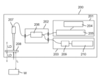
- FIG. 1 is a diagram showing the overall configuration of an SD-OCT (spectrometer type optical coherence tomography) device 200 as an example of an optical interference measurement device in the first embodiment.
- SD-OCT spectrometer type optical coherence tomography
- the SD-OCT apparatus 200 includes at least an optical frequency comb light source 201 having a low coherence light source 204 and an optical comb generation filter 205, light splitting means, and interference light detection means.
- the SD-OCT apparatus 200 further includes an optical fiber interferometer 202 and a spectrometer 203 having interference light detection means.
- the optical frequency comb light source 201 is a light source with an evenly spaced optical frequency distribution.
- the optical frequency comb light source 201 includes a low coherence light source 204 such as an SLD (superluminescent diode), an ultrashort pulse laser, or a supercontinuum light source, and low coherence light emitted from the low coherence light source 204 at equal intervals. It is composed of an optical comb generation filter 205 that adjusts the optical frequency distribution.
- the optical frequency of the light emitted from the low coherence light source 204 is shaped by the optical comb generation filter 205 into an optical frequency distribution with equal intervals, that is, into a comb shape with equal frequency intervals. Details of the optical frequency to be shaped will be described later.
- the optical fiber interferometer 202 has a coupler 206 connected to two light inlets and one light outlet.
- the light output port of the optical frequency comb light source 201 is connected to the first light receiving port of the two light receiving ports of the coupler 206.
- the optical output port of the coupler 206 is connected to a measurement head 207 outside the optical fiber interferometer 202. Light adjusted to equal frequency intervals by the optical comb generation filter 205 enters the measurement head 207 and is emitted toward the measurement target W.
- the light emitted from the measurement head 207 is split into measurement light and reference light by a reference surface 208, which is an example of a light splitting means.
- the reference surface 208 is not the end face of the collimator 30 on the measurement target W side as in the conventional case, but is located in the space between the measurement head 207 and the measurement target W, at a position away from the measurement head 207 on the measurement target W side, in other words. , are placed at a distance L from the measurement target W.
- the reference surface 208 in the first embodiment is a material that can separate light into transmitted light and reflected light.
- it can be configured with a half mirror or a parallel flat plate made of glass.
- the reference light enters the coupler 206 from the reference surface 208 via the measurement head 207, and enters the spectrometer 203 from the second light receiving port of the two light receiving ports of the coupler 206.
- the measurement light is irradiated from the reference surface 208 to the measurement object W that is separated by the distance L from the measurement object W, returns to the reference surface 208 through reflection or scattering on the measurement object W, and, like the reference light, is used for measurement.
- the light enters the coupler 206 through the head 207 and enters the spectroscope 203 from the second light receiving port of the coupler 206.
- the point where the signal optical path of the measurement light and the reference optical path of the reference light coincide is called a zero point.
- the zero point in this interferometer 202 is exactly the position of the reference plane 208, but this is not the case in the case of an interferometer with a different arrangement, such as a Michelson type.
- the spectrometer 203 has a diffraction grating 209 connected to the interferometer 202 and a detector array 210 connected to the diffraction grating 209.
- the two lights, the measurement light and the reference light are separated simultaneously by the diffraction grating 209 of the spectrometer 203, and they interfere in the optical frequency domain to become interference light in which the reflected light and the reference light are combined.As a result, the interference light
- the interference signal is measured by the detector array 210 as an example of interference light detection means.
- the sign of the optical path length difference is defined here as being determined by the sign of the calculation result of signal optical path length - reference optical path length.
- the maximum measurable range is a range of ⁇ LD around the zero point. If the frequency resolution dv is the optical frequency that can be resolved by one pixel of the detector array 210, the maximum time difference between the measurement light and the reference light observed by the spectrometer 203 is 1/2 dv according to Nyquist's sampling theorem. .
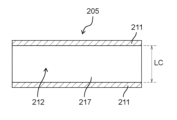
- the optical frequency comb generation filter 205 includes a pair of half mirrors 211 having a reflectance R as shown in FIG.
- a Fabry-Perot filter 212 constitutes an optical resonator.
- the output of the optical frequency comb light source 201 expressed in the frequency domain is shown in FIGS. 2B to 2D.
- the vertical axis represents optical output, transmittance, and optical output
- the horizontal axis represents optical frequency.
- the spectrum 300 (see FIG. 2B) of the original low-coherence light source 204 is multiplied by the transmittance spectrum 301 (see FIG. 2C) of the optical comb generation filter 205, and the modes with equal mode spacing FSR are The output spectrum is adjusted to a vertical comb-like output spectrum 302 (see FIG. 2D).
- the optical frequency comb light source 201 does not need to be a combination of the low coherence light source 204 and the optical comb generation filter 205, but may be a mode-locked laser with a stabilized repetition frequency or a single mode laser modulated by an electro-optic element.
- a comb-like mode or a high finesse etalon may be used, but since the linewidth of a single mode in the output spectrum of these is narrow band, as a result, the single mode of the optical frequency comb light source 201 is The coherence length defined by the line width becomes long, ranging from several tens of meters to more than 100 meters.
- the coherence length CO is about 30 m, so that the backscattered light generated by an optical element such as the coupler 206 is also the reference light from the reference surface 208.
- the interference occurs, resulting in an unnecessary interference signal that lowers the S/N ratio.
- the high finesse etalon has a low light transmittance, making it difficult to obtain a light intensity that satisfies the measurement dynamic range of the spectrometer 203, compared to the case where the output of the low coherence light source 204 is used as is.
- a Fabry-Perot filter that can control the single mode coherence length of the optical frequency comb light source 201 to be shorter than twice and less than 20 times the distance L from the zero point to the measurement target W. If the coherence length is less than twice the distance L, a sufficient interference signal cannot be obtained when the measurement range is doubled as described later. Furthermore, if the coherence length exceeds 20 times the distance L, the S/N ratio will decrease as described above, and the light transmittance will further decrease.
- the line width of the maximum transmittance peak of the Fabry-Perot filter 212 is 1/2 to 1/20 of the mode spacing FSR. This can be realized by setting the reflectance R of the half mirror pair 211 constituting the Fabry-Perot filter 212 to 20% and 85%, respectively.
- the optical comb generation filter 205 is a Fabry-Perot filter 212 with a finesse of 2 to 20, and that the mode spacing FSR thereof is randomly modulated as described later.
- the coupler 206 is used to combine light, but the optical fiber interferometer 202 may be constructed in free space using a beam splitter, or may be replaced with an element such as an optical circulator.
- the optical comb generation filter 205 that adjusts the spectrum of the low-coherence light source 204 does not have to be a resonator using an air gap 217 like the Fabry-Perot filter 212, but may be a resonator time delay mechanism using a fiber resonator.
- FIG. 3 is an explanatory diagram showing a first modification of the optical comb generation filter 205 in the first embodiment.
- Modification 1 of the optical comb generation filter 205 is a resonator coupler 400 having a first input port 401, a second input port 405, and two output ports 402, 403.
- the output of the low coherence light source 204 is incident on the first input port 401 of the resonator coupler 400.
- the incident light is split into two output ports 402 and 403 by the resonator coupler 400, and the output of the first output port 402 is incident on the optical fiber interferometer 202.
- the output of the second output port 403 is connected to the second input port 405 of the resonator coupler 400 via a time delay fiber 404 with optical path length LF.
- a time delay corresponding to the optical path length of the time delay fiber 404 can be provided to the output of the low coherence light source 204.
- This time delay corresponds to optical resonators placed facing each other with a cavity length LC/2.
- Modification 1 does not require precise alignment and is easier to adjust, especially when providing a long time delay, compared to a resonator using an air gap 217 such as the Fabry-Perot filter 212.
- FIG. 4 shows the coherence region of the SD-OCT apparatus 200 in the first embodiment.
- the range of optical path length differences in which an interference signal can be obtained is referred to as a coherent region.
- the intensity of the interference signal is constant, and the width is a rectangle of ⁇ LD.
- an interference signal is detected in the optical path length difference range of 0 ⁇ LD. This is defined as the zero-order coherence region.
- the optical path length difference between the signal optical path and the reference optical path is further separated by +2LC, that is, when the depth z is further separated by +LC
- an interference signal can be obtained even in the region of depth LC ⁇ LD.
- the time difference between light with a time delay of 2LC/c x (n+1) and light with a time delay of 2LC/c x n due to the optical comb generation filter 205 is zero. It can be considered that the interference is resolved when the round trip time difference between the point and the measurement target W is 2LC/c.
- an interference signal can be similarly obtained in the region of depth 2LC ⁇ LD.
- the range of the cavity length LC is the distance L from the zero point to the measurement target W. LC ⁇ 1-LD ⁇ L ⁇ LC ⁇ 1+LD (6) It is preferable that the cavity length LC is set to fall within the range of .
- the cavity length LC is made large, the resonator length in the optical comb generation filter 205 becomes long. There is no problem even if the above interference is used.
- LC 1/(2FSR)*c
- the distance ([1/(2FSR)*c*n] - LD) obtained by subtracting the measurable range LD determined by the optical frequency resolution dv of the spectrometer 203 from the value (i.e.
- the distance be within the distance ([1/(2FSR)*c*n]+LD) obtained by adding the measurable range LD to the above value (i.e., 1/(2FSR)*c*n).
- FIG. 5 shows a diagram of the measurement head 207 provided with the strength adjustment mechanism 213 and the coherent region.
- the intensity adjustment mechanism 213 is an element such as an aperture whose diameter can be changed or a variable ND (Neutral Density) filter, and by adjusting the intensity of only the reference light, the intensity of the signal light and the intensity of the reference light become equal, An interference signal with good contrast can be obtained.
- ND Neutral Density
- the intensity adjustment mechanism 213 is set at a position of depth + LC/2 from the zero point, which is between the zero-order interference area and the first-order interference area. In other words, it is installed at a distance from the zero point that is 1/4 of the value obtained by multiplying the reciprocal of the mode spacing FSR of the optical comb generation filter 205 by the speed of light c.
- the intensity adjustment mechanism 213 can minimize the contribution of the generated backscattered light to the interference signal.
- FIG. 6A shows the variation in the number of incident modes for the detector array 210. For example, if the center wavelength is 1310 nm and the wavelength width is 100 nm, and the spectrometer has 1024 pixels, the frequency resolution dv per pixel of the detector array 210 is 17 GHz.
- the mode interval FSR of the optical comb generation filter 205 is 17 GHz, which is the same as the frequency resolution dv
- the number of modes incident on each pixel is fixed at one, but if it is 10 GHz, for example, the number of modes incident on each pixel is The number of incident modes is a mixture of one and two. This variation results in intensity variation of each pixel, which causes deterioration of the S/N ratio of the SD-OCT apparatus 200.
- the optical comb generation filter 205 modulates the mode spacing FSR within the exposure time of the detector array 210 to reduce the influence of variations in the number of incident modes.
- the center wavelength of 1310 nm corresponds to the 22900th mode counting from 0 Hz. Therefore, when the mode interval FSR is changed to FSR+df during the exposure time, the wavelength of the 22,900th mode moves by 22,900 ⁇ df.
- the pixels of the spectrometer that each mode enters change, so that the quantized state as shown in FIG. 6A can be eliminated.
- the cavity length LC may be directly modulated by a linear motion mechanism such as a piezo element, or a vibration mechanism or especially a fiber may be used.
- a linear motion mechanism such as a piezo element, or a vibration mechanism or especially a fiber may be used.
- temperature modulation of the fiber may be used.
- the modulation width df of the mode should preferably change by about 0.5 pixel during the exposure time so as not to impair the contrast of the interference fringes themselves.
- the mode interval FSR changes sinusoidally or sawtoothly with respect to time
- sufficient averaging will not be achieved due to the correlation with the exposure time of the detector array 210.
- random modulation is preferable.
- Mechanisms for randomly modulating the mode spacing include, for example, randomly displacing one mirror of a mirror pair using a piezo element, or mechanically vibrating one or both mirrors of a mirror pair. can do.
- the reference surface 208 which is an example of a light splitting means, is arranged at a position away from the measurement head 207 toward the measurement object, and the light adjusted to equal frequency intervals by the optical comb generation filter 205 is transmitted.
- the detector array 210 which is an example of an interference light detection means, a common path is detected.
- the distance L to the measurement target W can be made longer than the measurable range LD.
- Embodiment 2 will be described using FIG. 7 showing the overall configuration of SD-OCT apparatus 500 in Embodiment 2.
- the same reference numerals are used for the same components as those of the first embodiment described in FIG. 1, and the explanation thereof will be omitted.
- the optical fiber interferometer 501 in the second embodiment is a Michelson interferometer rather than a common path interferometer, and the reference surface 208 is not placed at a position away from the measurement head 207 toward the measurement target W, but rather at a coupler. It is arranged at an independent position not passing through the measurement head 207 branched by 502. Therefore, the second embodiment has an advantage over the first embodiment in that the position of the zero point can be determined freely.
- the coupler 502 is used instead of the reference surface 208.
- the light output port of the optical frequency comb light source 201 is connected to the first light receiving port of the two light receiving ports of the optical fiber interferometer 501, and the coupler At 502, the beam is divided into a measurement beam and a reference beam.
- the light output port of the coupler 502 is connected to the measurement head 207 outside the optical fiber interferometer 501 as a signal light, and is also connected to the collimating lens 503 which enters the reference surface 208 as a reference light.
- the reference light enters the coupler 502 via the collimating lens 503 after being reflected on the reference surface 208, and enters the spectroscope 203 from the second light receiving port of the two light receiving ports of the optical fiber interferometer 501.
- the measurement light is irradiated onto the measurement object W from the measurement head 207, enters the coupler 502 from the measurement head 207 through reflection or scattering on the measurement object W, and passes through the second light receiving port of the optical fiber interferometer 501 to the spectrometer 203. incident on the
- the point where the signal optical path length of the measurement light and the reference optical path length of the reference light match is shown in FIG.
- the position of the zero point in the second embodiment can be freely varied, for example, by changing the distance between the collimating lens 503 and the reference surface 208 or the distance in the fiber between the coupler 502 and the collimating lens 503. For example, it can also be placed between the measuring head 207 and the coupler 502.
- the measurement target W is determined from the position of LC ⁇ n ⁇ LD from the zero point, that is, from a value that is an integral multiple of the reciprocal of the mode spacing FSR of the optical comb generation filter 205 multiplied by the speed of light c, and the optical frequency resolution of the spectrometer 203. It is within the range from the distance obtained by subtracting the measurable range LD determined by dv to the distance obtained by adding the measurable range LD to the above value.
- the light adjusted to equal frequency intervals by the optical comb generation filter 205 is split into the measurement light and the reference light by the coupler 502, which is an example of a light splitting means, and the
- the distance from The measurable range LD determined by the optical frequency resolution dv of the device array 210 is set within the adjusted distance range, and the interference light is detected by combining the reflected light from the measurement target W of the measurement light and the reference light. Detection is performed using a detector array 210, which is an example of means. With this configuration, the distance L to the measurement target W can be made longer than the measurable range LD.
- the reference surface 208 in Embodiment 2 does not need to be able to transmit light, and may be a mirror.
- the light adjusted to equal frequency intervals by the optical comb generation filter is split into the measurement light and the reference light by the light splitting means, and the light is split at the zero point.
- the measurable range determined by the optical frequency resolution of the interference light detection means is determined from a value that is an integral multiple of the reciprocal of the mode spacing of the optical comb generation filter multiplied by the speed of light.
- the interference light detection means detects interference light, which is a combination of the measurement light reflected from the object to be measured and the reference light, within the adjusted distance range. With this configuration, the distance to the measurement target can be made longer than the measurable range.
- the optical interference measurement device has the feature of being able to perform long-distance measurement even with high precision, and can be applied to applications such as precision measurement in the industrial field.
Abstract
光コム発生フィルタ205により等周波数間隔に調整された光が入射されて測定ヘッド207から測定対象Wに照射するとき、光コム発生フィルタ205により等周波数間隔に調整された光を測定光と参照光とに光分割手段208で分割し、測定光の測定対象Wからの反射光と参照光とが合波された干渉光を干渉光検出手段210で検出する。
Description
本発明は、反射光と参照光とによる干渉光を用いて測定対象を計測する光干渉計測装置に関するものである。
オプティカルコヒーレンストモグラフィー(すなわちOCT)は、光の干渉現象を利用した塗装膜などの構造物又は生体の断層像撮影法である。OCTは、眼科医療分野では既に実用化され、十数μmという高い分解能を持った断層計測手法として、眼球内の網膜などの微細領域の断層像撮影に用いられてきた。
OCTの中には、参照平面の走査が必要な時間領域OCT(すなわちTD-OCT)と参照平面の走査が不要な周波数領域OCT(すなわちFD-OCT)の2種類がある。FD-OCTの中にもスペクトロメータタイプ(すなわちSD-OCT)と波長走査型光源タイプ(すなわちSS-OCT)との2つがあるが、どちらも、光源から射出された光を測定光と参照光とに分割した後、測定対象から反射された測定光と参照光とを合波し、測定光と参照光との干渉光のビート周波数に基づいて光断層画像を取得するものである。
図8は、特許文献1に記載された従来のSD-OCT装置を示す図である。
図8に示す装置中の干渉計10において、光源12から射出された光はコリメータ30の端面で参照光と測定光に分割され、参照光はそのまま分光装置40へ、測定光は測定対象Wから反射されたのちにコリメータ30を経て同様に分光装置40へ入射する。ここでコリメータ30の端面は光干渉計における参照面として動作する。
分光装置40において測定光と参照光はスペクトル領域で干渉し、結果、干渉信号として干渉縞が計測される。この干渉信号に対して適当な信号処理を行うことで、測定対象Wの深さ方向1次元の屈折率分布の微分、つまり、反射率分布すなわち光断層画像を得ることが可能となる。
このように、参照光と測定光との分岐部を、干渉計10ではなく測定対象Wの付近に、ここではコリメータ30の測定対象W側の端面に、設置している。参照光と測定光とがほとんど同一の光路を通る光学系はコモンパス光学系と呼ばれ、参照光と測定光とが波長分散又は熱膨張による光路長の変動などの外乱を共有し打ち消しあうことから、コモンパス光学系は高い精度を持つ。
本発明の1つの態様にかかる光干渉計測装置は、低コヒレンス光を射出する低コヒレンス光源と、
前記低コヒレンス光源から射出された前記光を等間隔の光周波数分布に調整する光コム発生フィルタと、
前記光コム発生フィルタにより等周波数間隔に調整された光を測定光と参照光とに分割する光分割手段と、
前記測定対象からの反射光と前記参照光とが合波された干渉光を検出する干渉光検出手段と、
を備え、
前記測定光である信号光の信号光路長と前記参照光の参照光路長とが一致するゼロ点から前記測定対象までの距離を、前記光コム発生フィルタのモード間隔の逆数に光速を掛けた値の整数倍となる値から、前記干渉光検出手段の光周波数分解能により決定される測定可能範囲を減じた距離から、前記値に前記測定可能範囲を足した距離までの範囲内とする。
SD-OCT装置において測定可能な深さ方向の測定可能範囲LD、すなわち正しくスペクトル干渉縞を得ることができる参照光と測定光との光路長差の最大値の半分は、分光器の光周波数分解能によって制限される。そのため、前記従来の構成では、参照光と測定光との分岐部であるコリメータ30の測定対象W側の端面を基準とした測定対象Wまでの距離Lを、測定可能範囲LDより大きくとることができず、測定対象Wにコリメータ30を近接させた計測しか行うことができないという課題を有している。
本発明は、前記従来の課題を解決するもので、高い精度を維持しながら測定可能範囲より遠くの対象を測ることができる光干渉計測装置を提供することを目的とする。
以下、本発明の実施の形態について、図面を参照しながら説明する。
<実施の形態1>
図1は、実施の形態1における光干渉計測装置の一例としてのSD-OCT(スペクトロメータタイプ オプティカルコヒーレンストモグラフィー)装置200の全体構成を示す図である。
図1は、実施の形態1における光干渉計測装置の一例としてのSD-OCT(スペクトロメータタイプ オプティカルコヒーレンストモグラフィー)装置200の全体構成を示す図である。
SD-OCT装置200は、少なくとも、低コヒレンス光源204と光コム発生フィルタ205とを有する光周波数コム光源201と、光分割手段と、干渉光検出手段とを備えている。図1では、SD-OCT装置200は、さらに、光ファイバ干渉計202と、干渉光検出手段を有する分光器203とを備えている。
光周波数コム光源201は、等間隔の光周波数分布を持つ光源である。光周波数コム光源201は、SLD(スーパールミネッセントダイオード)、超短パルスレーザー、又はスーパーコンティニュウム光源などの低コヒレンス光源204と、低コヒレンス光源204から射出された低コヒレンス光を等間隔の光周波数分布に調整する光コム発生フィルタ205とで構成されている。低コヒレンス光源204から出た光は、光コム発生フィルタ205により、等間隔の光周波数分布すなわち等周波数間隔のコム状に光周波数を成形される。成形される光周波数の詳細については後述する。
光周波数コム光源201から発生した光は、光ファイバ干渉計202に入射する。光ファイバ干渉計202は、2つの光受入口と1つの光送出口とに接続されているカプラ206を有する。
光ファイバ干渉計202において、光周波数コム光源201の光出射口が、カプラ206の2つの光受入口のうちの第1光受入口に接続されている。カプラ206の光送出口は光ファイバ干渉計202外の測定ヘッド207に接続されている。測定ヘッド207には、光コム発生フィルタ205により等周波数間隔に調整された光が入射されて測定対象Wに向けて出射される。
測定ヘッド207から出射した光は、光分割手段の一例としての参照面208により測定光及び参照光に分割される。参照面208は、従来のようにコリメータ30の測定対象W側の端面ではなく、測定ヘッド207と測定対象Wとの間の空間に、測定ヘッド207から測定対象W側に離れた位置、言い換えれば、測定対象Wからは距離Lだけ離れた位置に配置されている。
実施の形態1における参照面208は、光を透過光と反射光に分離することができる素材である。一例として、ハーフミラー、又はガラス製の平行平板などで構成することができる。
参照光は、参照面208から測定ヘッド207を経てカプラ206に入り、カプラ206の2つの光受入口のうち第2光受入口から分光器203へ入射する。一方、測定光は、参照面208から、測定対象Wまでの距離Lだけ離れた測定対象Wに照射され、測定対象Wにおける反射又は散乱を経て参照面208に戻り、参照光と同様に、測定ヘッド207を経てカプラ206に入り、カプラ206の第2光受入口から分光器203へ入射する。
干渉計202において、測定光の信号光路と参照光の参照光路とが一致する点をゼロ点と称する。本干渉計202においてのゼロ点は参照面208の位置そのものとなるが、マイケルソン型など異なる配置の干渉計の場合はその限りではない。
分光器203は、干渉計202に接続される回折格子209と、回折格子209に接続される検出器アレイ210とを有している。分光器203の回折格子209によって測定光と参照光との二つの光は同時に分光され、光周波数領域で干渉して反射光と参照光とが合波された干渉光となり、その結果、干渉光の干渉信号が干渉光検出手段の一例としての検出器アレイ210によって計測される。
この干渉信号に対して適当な信号処理を行うことで、測定対象Wの測定光の信号光路における1次元の屈折率分布の微分、つまり、反射率分布を得ることが可能となる。なお、ここでは、光路長差の正負の符号を、信号光路長-参照光路長の演算結果の正負により決定されると定義する。
このとき、前述したように、SD-OCT装置200において測定可能な深さ方向の有限の測定可能範囲をLDとすると、測定可能な最大範囲は、ゼロ点を中心に±LDの範囲となる。検出器アレイ210の持つ1画素で分解可能な光周波数を周波数分解能dvとすると、分光器203で観測される測定光及び参照光の最大の時間差は、ナイキストのサンプリング定理より、1/2dvである。これは、深さ、すなわち往復の距離に換算すると、光速をcとして
LD=c/4dv・・・(1)
と表され、分光器203の周波数分解能dvが良いほど測定可能範囲LDは大きくなるが、周波数分解能dvは、検出器アレイ210の持つ有限の画素数で制限されるため、限界がある。
LD=c/4dv・・・(1)
と表され、分光器203の周波数分解能dvが良いほど測定可能範囲LDは大きくなるが、周波数分解能dvは、検出器アレイ210の持つ有限の画素数で制限されるため、限界がある。
<光周波数コム発生器について>
光周波数コム発生器である光周波数コム光源201により生成される出力スペクトルについて図2A~図2Dを用いて説明する。光コム発生フィルタ205は一例として、図2Aで示されるような反射率Rを持つ2枚のハーフミラー対211を一定のエアギャップ距離、すなわちキャビティ長LCのエアギャップ217を挟んで対向して配設された光共振器を構成した、ファブリペローフィルタ212である。この光コム発生フィルタ205を透過した低コヒレンス光源204の出力は、時間領域においては
2LC/c×n ・・・ (2)
の時間遅れが付与される。nは光共振器内の光の往復回数であって、n=0,1,2,3である。
光周波数コム発生器である光周波数コム光源201により生成される出力スペクトルについて図2A~図2Dを用いて説明する。光コム発生フィルタ205は一例として、図2Aで示されるような反射率Rを持つ2枚のハーフミラー対211を一定のエアギャップ距離、すなわちキャビティ長LCのエアギャップ217を挟んで対向して配設された光共振器を構成した、ファブリペローフィルタ212である。この光コム発生フィルタ205を透過した低コヒレンス光源204の出力は、時間領域においては
2LC/c×n ・・・ (2)
の時間遅れが付与される。nは光共振器内の光の往復回数であって、n=0,1,2,3である。
光周波数コム光源201の出力を周波数領域で表したものを図2B~図2Dに示す。図2B~図2Dでは、縦軸に光出力、透過率、光出力をとり、横軸に光周波数をとっている。
この光コム発生フィルタ205では、本来の低コヒレンス光源204のスペクトル300(図2B参照)に、光コム発生フィルタ205の透過率スペクトル301(図2C参照)が乗算され、等しいモード間隔FSRのモードが立つコム状の出力スペクトル302(図2D参照)に調整される。
このときのモード間隔FSRは、光速cとキャビティ長LCを用いて
FSR=c/2LC・・・(3)
で表される。
FSR=c/2LC・・・(3)
で表される。
ここで、光周波数コム光源201は、低コヒレンス光源204に光コム発生フィルタ205を組み合わせたものでなくとも、繰り返し周波数を安定化させたモードロックレーザ、又は、シングルモードレーザを電気光学素子で変調させコム状のモードにしたもの、又は、高フィネスなエタロンでもよいが、これらは出力スペクトルにおける単一モードの線幅が狭帯域であるため、結果として、光周波数コム光源201の単一モードの線幅で定義されるコヒレンス長が、数十~百m以上と長くなる。具体的には、単一モードの線幅をΔfとすると、その単一モードのコヒレンス時間Tは、
T=1/Δf・・・(4)
となる。このコヒレンス時間Tによるコヒレンス長COは、深さに換算して、
CO=T*c/2=c/2Δf・・・(5)
となる。
T=1/Δf・・・(4)
となる。このコヒレンス時間Tによるコヒレンス長COは、深さに換算して、
CO=T*c/2=c/2Δf・・・(5)
となる。
例えばFSR=10GHz、フィネスが2000程度の高フィネスエタロンの場合、コヒレンス長COは30m程度にもなるため、例えばカプラ206などの光学素子で生じた後方散乱光なども参照面208からの参照光と干渉してしまい、不要な干渉信号としてS/N比を低下させてしまうという問題がある。また、高フィネスエタロンは光の透過率が低く、低コヒレンス光源204の出力をそのまま用いる場合に比べ、分光器203の測定ダイナミックレンジを満たす光強度を得ることが困難である。
そのため、光周波数コム光源201の単一モードのコヒレンス長は、ゼロ点から測定対象Wまでの距離Lの2倍以上、20倍以下に短くコントロールできるファブリペローフィルタが好ましい。コヒレンス長が距離Lの2倍より低い場合、後述するように計測範囲を2倍に拡張した際に、十分な干渉信号を得ることができない。また、コヒレンス長が距離Lの20倍を超える場合、前述のようにS/N比を低下させ、さらに光の透過率が低くなってしまう。
これを実現させるには、ファブリペローフィルタ212の透過率の極大値のピークの線幅はモード間隔FSRの1/2~1/20となる。これは、ファブリペローフィルタ212を構成するハーフミラー対211の反射率Rをそれぞれ20%、85%に設定することで実現することができる。
よって、光コム発生フィルタ205が、フィネス2~20の範囲であるファブリペローフィルタ212であり、そのモード間隔FSRを後述するようにランダムに変調される機構とするのが好ましい。
ここでは光の合波にカプラ206を用いているが、光ファイバ干渉計202をビームスプリッタを用いて自由空間で構築してもよいし、光サーキュレータなどの素子を用いて代用してもよい。
低コヒレンス光源204のスペクトルを調整する光コム発生フィルタ205は、ファブリペローフィルタ212のようなエアギャップ217を用いた共振器でなくとも、ファイバ共振器を用いた共振器時間遅延機構としてもよい。
<光コム発生フィルタ205の変形例1>
図3は本実施形態1における光コム発生フィルタ205の変形例1を示す説明図である。光コム発生フィルタ205の変形例1は、第一の入力ポート401と第二の入力ポート405と2つの出力ポート402、403とを有する共振器カプラ400である。
図3は本実施形態1における光コム発生フィルタ205の変形例1を示す説明図である。光コム発生フィルタ205の変形例1は、第一の入力ポート401と第二の入力ポート405と2つの出力ポート402、403とを有する共振器カプラ400である。
低コヒレンス光源204の出力は、共振器カプラ400の第一の入力ポート401に入射する。入射した光は、共振器カプラ400によって2つの出力ポート402、403に分岐され、第一の出力ポート402の出力は、光ファイバ干渉計202に入射する。
第二の出力ポート403の出力は、光路長LFの時間遅延ファイバ404を経て共振器カプラ400の第二の入力ポート405に接続される。
この構成により、低コヒレンス光源204の出力に時間遅延ファイバ404の光路長に相当する時間遅延を設けることができる。この時間遅延は、キャビティ長LC/2で対向し配設された光共振器に相当する。
変形例1は、特に長い時間遅延を設ける際に、ファブリペローフィルタ212のようなエアギャップ217を用いた共振器に比べて、精密なアライメントを行う必要がなく、調整が容易である。
<深さレンジの拡大について>
図4に実施の形態1におけるSD-OCT装置200の可干渉領域を示す。ここでは、干渉信号を得ることが可能な光路長差の範囲を、可干渉領域と称する。可干渉領域は、縦軸に干渉信号の強度、横軸に深さz(=光路長差/2)をとった際に、ゼロ点を中心としたローレンツ関数を描くが、ここでは簡単のため、干渉信号の強度一定、幅は±LDの矩形とする。
図4に実施の形態1におけるSD-OCT装置200の可干渉領域を示す。ここでは、干渉信号を得ることが可能な光路長差の範囲を、可干渉領域と称する。可干渉領域は、縦軸に干渉信号の強度、横軸に深さz(=光路長差/2)をとった際に、ゼロ点を中心としたローレンツ関数を描くが、ここでは簡単のため、干渉信号の強度一定、幅は±LDの矩形とする。
信号光路と参照光路の光路長差が0であるゼロ点の付近では、光路長差0±LDの範囲で干渉信号が検出される。これを、0次の可干渉領域とする。
さらに、信号光路と参照光路の光路長差がさらに+2LCだけ離れたとき、すなわち深さzが+LCだけ離れたときには、深さLC±LDの領域でも干渉信号を得ることができる。これは、時間領域で考えると、光コム発生フィルタ205により2LC/c×(n+1)の時間遅延を持った光と、2LC/c×nの時間遅延を持った光が、それぞれの時間差をゼロ点と測定対象Wの間の往復の時間差2LC/cをもって解消し、干渉したと考えることができる。
同様に、信号光路と参照光路の光路長差がさらに+2LCだけ離れたときにも、同様に深さ2LC±LDの領域で干渉信号を得ることができる。
このように、ゼロ点から深さn×LC(ただし、n=1,2,3・・)だけ離れた領域で生じる干渉を、n次の干渉と称する。
よって、本実施の形態1は、n次の干渉を用い(ただし、n=1,2,3・・)、ゼロ点と測定対象Wの距離Lが測定可能範囲LDよりも大きいときの干渉信号を得ることができる。
nの範囲としては、光周波数コム光源201の単一モードの線幅で定義されるコヒレンス長の範囲であれば、どのような値をとっても干渉信号を得ることはできるものの、0次についで1次の干渉信号の強度が強いため、n=1次が好ましい。つまり、キャビティ長LCの範囲としては、ゼロ点から測定対象Wまでの距離Lが、
LC×1-LD < L < LC×1+LD ・・・(6)
の範囲に含まれるようにキャビティ長LCが設定されていることが好ましい。
LC×1-LD < L < LC×1+LD ・・・(6)
の範囲に含まれるようにキャビティ長LCが設定されていることが好ましい。
ただし、キャビティ長LCを大きくとると、光コム発生フィルタ205における共振器長が長大になるため、光周波数コム光源201の単一モードの線幅で定義されるコヒレンス長の範囲でn=2次以上の干渉を用いても問題ない。
この(6)式を言い換えると、(3)式のLC=1/(2FSR)*cより、測定光である信号光の信号光路長と前記参照光の参照光路長とが一致するゼロ点から測定対象Wまでの距離Lを、光コム発生フィルタ205のモード間隔FSRの逆数に2を除して光速cを掛けた値の整数倍(ただし、n=1,2,3・・)となる値(すなわち1/(2FSR)*c*n)から、分光器203の光周波数分解能dvにより決定される測定可能範囲LDを減じた距離([1/(2FSR)*c*n]-LD)から、前記値(すなわち1/(2FSR)*c*n)に測定可能範囲LDを足した距離([1/(2FSR)*c*n]+LD)までの範囲内とすることが好ましいことになる。
<信号光強度の調整機構について>
SD-OCT装置200において、検出器アレイ210の有限のダイナミックレンジ内でコントラストの良い干渉信号を得るために、測定光である信号光の強度と参照光の強度が等しくなることが望ましい。しかし、コモンパス干渉計では、参照光は常に信号光と同じ光路を通り、参照光のみの強度を調整することは困難であるため、測定ヘッド207には、ゼロ点から測定対象Wまでの間の信号光側に強度調整機構213を設けても良い。
SD-OCT装置200において、検出器アレイ210の有限のダイナミックレンジ内でコントラストの良い干渉信号を得るために、測定光である信号光の強度と参照光の強度が等しくなることが望ましい。しかし、コモンパス干渉計では、参照光は常に信号光と同じ光路を通り、参照光のみの強度を調整することは困難であるため、測定ヘッド207には、ゼロ点から測定対象Wまでの間の信号光側に強度調整機構213を設けても良い。
図5に強度調整機構213を設けた測定ヘッド207と可干渉領域の図を示す。強度調整機構213は、例えば口径を変えられるアパーチャ又は可変のND(Neutral Density)フィルタなどの素子であり、参照光のみの強度を調整することにより信号光の強度と参照光の強度が等しくなり、コントラストの良い干渉信号を得ることができる。
強度調整機構213は、素子端面の反射が干渉信号として検出されてしまうことを防ぐために、0次の干渉領域と1次の干渉領域との中間であるゼロ点からの深さ+LC/2の位置、言い換えれば、ゼロ点から光コム発生フィルタ205のモード間隔FSRの逆数に光速cを掛けた値の1/4の距離の位置に設置されている。
これにより、強度調整機構213は、生じた後方散乱光が干渉信号に寄与することを最小限に抑えることができる。
なお、同様に、0次の干渉領域と-1次の干渉領域の中間である深さ-LC/2にも干渉信号として検出されない領域が生じるが、このような光路長差が負の領域では、信号光と参照光は参照面208に達しておらず、同じ光路を通っているため、強度調整機構213を設置することは好ましくない。
<分光器の離散防止>
光周波数コム光源201が発生させるスペクトルは、分光器203の検出器アレイ210に入射する際に、検出器アレイ210の1画素あたりに入射するモード数に量子化誤差によるバラツキが生じる。図6Aは検出器アレイ210に対する入射モード数のバラツキを示したものである。例えば中心波長1310nm、波長幅100nmを1024画素の分光器で均一に分光したとすると、検出器アレイ210の1画素あたりの周波数分解能dvは17GHzである。このとき、光コム発生フィルタ205のモード間隔FSRが周波数分解能dvと同じく17GHzであれば、1画素あたりに入射するモード数は1本で固定されるが、例えば10GHzである場合は1画素あたりに入射するモード数は1本と2本が混在する。このバラツキは各画素の強度バラツキとなり、SD-OCT装置200のS/N比を劣化させる原因となる。
光周波数コム光源201が発生させるスペクトルは、分光器203の検出器アレイ210に入射する際に、検出器アレイ210の1画素あたりに入射するモード数に量子化誤差によるバラツキが生じる。図6Aは検出器アレイ210に対する入射モード数のバラツキを示したものである。例えば中心波長1310nm、波長幅100nmを1024画素の分光器で均一に分光したとすると、検出器アレイ210の1画素あたりの周波数分解能dvは17GHzである。このとき、光コム発生フィルタ205のモード間隔FSRが周波数分解能dvと同じく17GHzであれば、1画素あたりに入射するモード数は1本で固定されるが、例えば10GHzである場合は1画素あたりに入射するモード数は1本と2本が混在する。このバラツキは各画素の強度バラツキとなり、SD-OCT装置200のS/N比を劣化させる原因となる。
これを防ぐため、光コム発生フィルタ205は、検出器アレイ210の露光時間内にモード間隔FSRを変調することで、入射するモード数のバラツキの影響を低減する。
図6Bにその概要を示す。
例えばモード間隔FSRが10GHz、LC=15mmのとき、中心波長1310nmは0Hzから数えて22900本目のモードに相当する。そのため、露光時間中にモード間隔FSRをFSR+dfへと変化させると、22900本目のモードである波長は22900×df移動する。これにより、各モードが入射する分光器の画素が変化するため、図6Aのような量子化された状態を解消することができる。
モード間隔FSRを走査する手段としては、エアギャップ217を用いたファブリペローフィルタ212においてはピエゾ素子などの直動機構で直接キャビティ長LCを変調してもよいし、振動機構又は、特にファイバを用いた光コム発生フィルタ205の変形例1においてはファイバに対する温度変調を用いてもよい。
モードの変調幅dfとしては干渉縞自体のコントラストを損なわないため、露光時間中に0.5画素程度の変化がよい。これに相当する光周波数の変化は8.5GHz程度であり、中心波長1310nmにおいて8.5GHzのシフトを実現するモード間隔FSRの変化量は、
8.5GHz/22900=370kHz ・・・(5)
である。これは、15mmのキャビティにおいて約1μmのシフトに相当する。
8.5GHz/22900=370kHz ・・・(5)
である。これは、15mmのキャビティにおいて約1μmのシフトに相当する。
モードの変調波形としては、例えば時間に対しモード間隔FSRが正弦波状又はノコギリ状に変化するような周期的な手法を用いると、検出器アレイ210の露光時間との相関により十分に平均化がされない懸念があるため、ランダムに変調させることが好ましい。モード間隔をランダムに変調される機構としては、例として、ミラー対の片側のミラーをピエゾ素子でランダムに変位させる、もしくは、ミラー対の片側もしくは両側のミラーを機械的に振動させる、などで構成することができる。
前記実施の形態1によれば、測定ヘッド207から測定対象側に離れた位置に配置された光分割手段の一例の参照面208により、光コム発生フィルタ205により等周波数間隔に調整された光を測定光と参照光とに分割し、測定光の測定対象Wからの反射光と参照光とが合波された干渉光を干渉光検出手段の一例の検出器アレイ210で検出することにより、コモンパス光学系において測定対象Wまでの距離Lを測定可能範囲LDより遠くすることができる。
<実施の形態2>
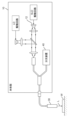
実施の形態2について、実施の形態2におけるSD-OCT装置500の全体構成を示す図7を用いて説明する。図1にて説明した実施の形態1の構成要素と同じ構成要素については同じ符号を用いて、その説明を省略する。
実施の形態2について、実施の形態2におけるSD-OCT装置500の全体構成を示す図7を用いて説明する。図1にて説明した実施の形態1の構成要素と同じ構成要素については同じ符号を用いて、その説明を省略する。
本実施の形態2における光ファイバ干渉計501は、コモンパス干渉計ではなくマイケルソン干渉計であり、参照面208を、測定ヘッド207から測定対象W側に離れた位置に配置するのではなく、カプラ502により分岐された測定ヘッド207を経由しない独立した位置に配置されている。そのため、実施の形態2では、実施の形態1に比べてゼロ点の位置を自由に決めることができるという利点がある。ここでは、光分割手段の一例は、参照面208ではなく、カプラ502で機能させている。
光ファイバ干渉計202の代わりの光ファイバ干渉計501において、光周波数コム光源201の光出射口が、光ファイバ干渉計501の2つの光受入口のうちの第1光受入口に接続され、カプラ502で測定光及び参照光に分割される。カプラ502の光送出口は、信号光として光ファイバ干渉計501外の測定ヘッド207に接続されるとともに、参照光として参照面208に入射するコリメートレンズ503にも接続している。
参照光は、参照面208での反射を経てコリメートレンズ503を経てカプラ502に入り、光ファイバ干渉計501の2つの光受入口のうち第2光受入口から分光器203へ入射する。
一方、測定光は、測定ヘッド207から測定対象Wに照射され、測定対象Wにおける反射又は散乱を経て測定ヘッド207からカプラ502に入り、光ファイバ干渉計501の第2光受入口から分光器203へ入射する。
光ファイバ干渉計501において、測定光の信号光路長と参照光の参照光路長とが一致する点、すなわちゼロ点を図7中に示す。実施の形態2におけるゼロ点の位置は、例えばコリメートレンズ503と参照面208の距離、又は、カプラ502からコリメートレンズ503の間のファイバにおける距離を変えることで、自由に可変にすることができ、例えば測定ヘッド207とカプラ502の間に配することもできる。
測定対象Wは、ゼロ点からLC×n±LDの位置、すなわち光コム発生フィルタ205のモード間隔FSRの逆数に光速cを掛けた値の整数倍となる値から、分光器203の光周波数分解能dvにより決定される測定可能範囲LDを減じた距離から、前記値に前記測定可能範囲LDを足した距離までの範囲内にある。
以上のように、実施の形態2によれば、光コム発生フィルタ205により等周波数間隔に調整された光を測定光と参照光とに光分割手段の一例のカプラ502により分割し、前記ゼロ点から前記測定対象Wまでの距離を、前記光コム発生フィルタ205のモード間隔FSRの逆数に光速cを掛けた値の整数倍nとなる値に対して、前記干渉光検出手段の一例としての検出器アレイ210の光周波数分解能dvにより決定される測定可能範囲LDを加減した距離の範囲内とし、測定光の測定対象Wからの反射光と参照光とが合波された干渉光を干渉光検出手段の一例の検出器アレイ210で検出している。このように構成することにより、測定対象Wまでの距離Lを測定可能範囲LDより遠くすることができる。
なお、実施の形態2における参照面208は、光を透過できる必要はなく、ミラーでもよい。
なお、前記様々な実施の形態又は変形例のうちの任意の実施の形態又は変形例を適宜組み合わせることにより、それぞれの有する効果を奏するようにすることができる。また、実施の形態同士の組み合わせ又は実施例同士の組み合わせ又は実施の形態と実施例との組み合わせが可能であると共に、異なる実施の形態又は実施例の中の特徴同士の組み合わせも可能である。
以上のように、本発明の態様にかかる光干渉計測装置によれば、光コム発生フィルタにより等周波数間隔に調整された光を測定光と参照光とに光分割手段により分割し、前記ゼロ点から前記測定対象までの距離を、前記光コム発生フィルタのモード間隔の逆数に光速を掛けた値の整数倍となる値から、前記干渉光検出手段の光周波数分解能により決定される測定可能範囲を加減した距離の範囲内とし、測定光の測定対象からの反射光と参照光とが合波された干渉光を干渉光検出手段で検出している。このように構成することにより、測定対象までの距離を測定可能範囲より遠くすることができる。
本発明の前記態様にかかる光干渉計測装置は、高精度でも長距離の計測を可能とする特徴を有し、工業分野での精密測定などの用途にも適用できる。
10 干渉計
12 光源
30 コリメータ
40 分光装置
200 SD-OCT装置
201 光周波数コム光源
202 光ファイバ干渉計
203 分光器
204 低コヒレンス光源
205 光コム発生フィルタ
206 カプラ
207 測定ヘッド
208 参照面
209 回折格子
210 検出器アレイ
211 ハーフミラー対
212 ファブリペローフィルタ
213 強度調整機構
217 エアギャップ
300 低コヒレンス光源のスペクトル
301 光コム発生フィルタの透過率スペクトル
302 出力スペクトル
400 共振器カプラ
401 第一の入力ポート
402 第一の出力ポート
403 第二の出力ポート
404 時間遅延ファイバ
405 第二の入力ポート
500 SD-OCT装置
501 光ファイバ干渉計
502 カプラ
503 コリメートレンズ
LD 測定可能範囲
L 測定対象Wまでの距離
W 測定対象
dv 周波数分解能
LC キャビティ長
FSR モード間隔
FW モード幅
R 反射率
Claims (5)
- 低コヒレンス光を射出する低コヒレンス光源と、
前記低コヒレンス光源から射出された前記光を等間隔の光周波数分布に調整する光コム発生フィルタと、
前記光コム発生フィルタにより等周波数間隔に調整された光を測定光と参照光とに分割する光分割手段と、
前記測定対象からの反射光と前記参照光とが合波された干渉光を検出する干渉光検出手段と、
を備え、
前記測定光である信号光の信号光路長と前記参照光の参照光路長とが一致するゼロ点から前記測定対象までの距離を、前記光コム発生フィルタのモード間隔の逆数に光速を掛けた値の整数倍となる値から、前記干渉光検出手段の光周波数分解能により決定される測定可能範囲を減じた距離から、前記値に前記測定可能範囲を足した距離までの範囲内とする、
光干渉計測装置。 - 前記低コヒレンス光源は、スーパールミネッセントダイオードと、超短パルスレーザーと、スーパーコンティニュウム光源とのうちのいずれかの光源であり、その光源から射出された光が前記低コヒレンス光である、
請求項1に記載の光干渉計測装置。 - 前記光分割手段が、前記測定対象と前記測定ヘッドとの間に配置されている、
請求項1又は2に記載の光干渉計測装置。 - さらに、前記測定光である信号光の強度調整を行う強度調整機構を備え、
前記強度調整機構は、ゼロ点から前記光コム発生フィルタのモード間隔の逆数に光速を掛けた値の半分の距離の位置に配置されている、
請求項1又は2に記載の光干渉計測装置。 - 上記光コム発生フィルタが、フィネス2~20の範囲であるファブリペローフィルタであり、そのモード間隔をランダムに変調される機構である、
請求項4に記載の光干渉計測装置。
Applications Claiming Priority (2)
| Application Number | Priority Date | Filing Date | Title |
|---|---|---|---|
| JP2022073302 | 2022-04-27 | ||
| JP2022-073302 | 2022-04-27 |
Publications (1)
| Publication Number | Publication Date |
|---|---|
| WO2023210116A1 true WO2023210116A1 (ja) | 2023-11-02 |
Family
ID=88518433
Family Applications (1)
| Application Number | Title | Priority Date | Filing Date |
|---|---|---|---|
| PCT/JP2023/005270 WO2023210116A1 (ja) | 2022-04-27 | 2023-02-15 | 光干渉計測装置 |
Country Status (1)
| Country | Link |
|---|---|
| WO (1) | WO2023210116A1 (ja) |
Citations (9)
| Publication number | Priority date | Publication date | Assignee | Title |
|---|---|---|---|---|
| JP2004340581A (ja) * | 2003-05-13 | 2004-12-02 | Institute Of Tsukuba Liaison Co Ltd | 時間シアリング光コヒーレンストモグラフィー装置及び方法 |
| JP2009270939A (ja) * | 2008-05-08 | 2009-11-19 | Keyence Corp | 光学式変位計 |
| JP2011257160A (ja) * | 2010-06-04 | 2011-12-22 | Canon Inc | 光干渉断層撮像装置、光干渉断層撮像方法、およびプログラム |
| JP2012154728A (ja) * | 2011-01-25 | 2012-08-16 | Tokyo Univ Of Agriculture & Technology | 構造測定方法および構造測定装置 |
| JP2013029317A (ja) * | 2011-07-26 | 2013-02-07 | Hitachi High-Technologies Corp | 光断層画像測定装置および光断層画像測定システム |
| WO2016067570A1 (ja) * | 2014-10-27 | 2016-05-06 | 富士フイルム株式会社 | 光侵入深さ評価方法、その評価方法を用いた性能検査方法および光断層画像撮像装置 |
| JP2017181300A (ja) * | 2016-03-30 | 2017-10-05 | 国立大学法人名古屋大学 | 農作物観測方法、農作物観測装置および農作物の生産方法 |
| JP2019049481A (ja) * | 2017-09-11 | 2019-03-28 | 株式会社東京精密 | 校正装置及び校正方法 |
| JP2019512086A (ja) * | 2016-02-12 | 2019-05-09 | ザ ジェネラル ホスピタル コーポレイション | 光コヒ−レンストモグラフィを用いた高速・長深度レンジの撮像装置及び方法 |
-
2023
- 2023-02-15 WO PCT/JP2023/005270 patent/WO2023210116A1/ja unknown
Patent Citations (9)
| Publication number | Priority date | Publication date | Assignee | Title |
|---|---|---|---|---|
| JP2004340581A (ja) * | 2003-05-13 | 2004-12-02 | Institute Of Tsukuba Liaison Co Ltd | 時間シアリング光コヒーレンストモグラフィー装置及び方法 |
| JP2009270939A (ja) * | 2008-05-08 | 2009-11-19 | Keyence Corp | 光学式変位計 |
| JP2011257160A (ja) * | 2010-06-04 | 2011-12-22 | Canon Inc | 光干渉断層撮像装置、光干渉断層撮像方法、およびプログラム |
| JP2012154728A (ja) * | 2011-01-25 | 2012-08-16 | Tokyo Univ Of Agriculture & Technology | 構造測定方法および構造測定装置 |
| JP2013029317A (ja) * | 2011-07-26 | 2013-02-07 | Hitachi High-Technologies Corp | 光断層画像測定装置および光断層画像測定システム |
| WO2016067570A1 (ja) * | 2014-10-27 | 2016-05-06 | 富士フイルム株式会社 | 光侵入深さ評価方法、その評価方法を用いた性能検査方法および光断層画像撮像装置 |
| JP2019512086A (ja) * | 2016-02-12 | 2019-05-09 | ザ ジェネラル ホスピタル コーポレイション | 光コヒ−レンストモグラフィを用いた高速・長深度レンジの撮像装置及び方法 |
| JP2017181300A (ja) * | 2016-03-30 | 2017-10-05 | 国立大学法人名古屋大学 | 農作物観測方法、農作物観測装置および農作物の生産方法 |
| JP2019049481A (ja) * | 2017-09-11 | 2019-03-28 | 株式会社東京精密 | 校正装置及び校正方法 |
Non-Patent Citations (3)
| Title |
|---|
| CHOI SAMUEL, WATANABE TOMOYA, SUZUKI TAKAMASA, NIN FUMIAKI, HIBINO HIROSHI, SASAKI OSAMI: "Multifrequency swept common-path en-face OCT for wide-field measurement of interior surface vibrations in thick biological tissues", OPTICS EXPRESS, vol. 23, no. 16, 10 August 2015 (2015-08-10), pages 21078, XP093104914, DOI: 10.1364/OE.23.021078 * |
| MORIYOSHI CHOI , SHOGO MURAMATSU, SHUHANG REN, GAKU OTA , HIROSHI HIBINO : "Optical coherence microscope using high-speed CMOS image sensor for intracochlear vibration imaging", ITE TECHNICAL REPORT, EIZO JOHO MEDIA GAKKAI, TOKYO, JP, vol. 44, no. 29 (IST2020-50), 13 November 2020 (2020-11-13), JP , pages 35 - 40, XP009550057, ISSN: 1342-6893 * |
| TWAYANA KRISHNA, REBOLLEDO-SALGADO ISRAEL, DERIUSHKINA EKATERINA, SCHRÖDER JOCHEN, KARLSSON MAGNUS, TORRES-COMPANY VICTOR: "Spectral Interferometry with Frequency Combs", MICROMACHINES, vol. 13, no. 4, 14 April 2022 (2022-04-14), pages 614, XP093104911, DOI: 10.3390/mi13040614 * |
Similar Documents
| Publication | Publication Date | Title |
|---|---|---|
| US7929148B2 (en) | Optical coherence tomography implementation apparatus and method of use | |
| JP5265918B2 (ja) | モード選択同調器からの光フィードバック | |
| JP5711134B2 (ja) | フーリエドメインモードロッキング | |
| US6160826A (en) | Method and apparatus for performing optical frequency domain reflectometry | |
| EP2280256B1 (en) | Method and apparatus for performing optical imaging using frequency-domain interferometry | |
| US8488125B2 (en) | Optical tomography apparatus with timing detection element including optical resonator having variable resonator length | |
| US8632181B2 (en) | SS OCT interferometry for measuring a sample | |
| US8363226B2 (en) | Optical interference measuring apparatus | |
| US20150109622A1 (en) | Optical coherence tomography apparatus and optical coherence tomography method | |
| US10330462B2 (en) | System for analyzing optical properties of an object | |
| US10816408B1 (en) | Wavelength shifting in spectrally-controlled interferometry | |
| KR101987392B1 (ko) | 고속 빗살 파장 가변 광원 장치 및 이를 이용하는 원거리 형상 변화 고속 측정을 위한 장치 | |
| US10641599B2 (en) | Extending the range of spectrally controlled interferometry by superposition of multiple spectral modulations | |
| WO2023210116A1 (ja) | 光干渉計測装置 | |
| US11385044B2 (en) | Extending the range of spectrally controlled interferometry by superposition of multiple spectral modulations | |
| US20140125992A1 (en) | Optical coherence tomography apparatus and optical coherence tomography method | |
| JP5654837B2 (ja) | 変位測定装置 | |
| KR101108693B1 (ko) | 백색광 간섭계를 기반으로 하는 굴절률 측정 장치 및 방법 | |
| WO2010113985A1 (ja) | 干渉計 | |
| Schwider | Coarse frequency comb interferometry | |
| US20120274943A1 (en) | Fizeau reference arm using a chirped fiber bragg grating | |
| Harder et al. | Adaptive frequency comb illumination for interferometry in the case of nested two-beam cavities | |
| Choi et al. | Profilometry using Fizeau-interferometer based on optical comb interferometry and sinusoidal phase modulation method | |
| Schwider | Coarse‐Frequency‐Comb Multiple‐Beam Interferometry: Phase Assessment Using Common Phase Shifting Procedures |
Legal Events
| Date | Code | Title | Description |
|---|---|---|---|
| 121 | Ep: the epo has been informed by wipo that ep was designated in this application |
Ref document number: 23795864 Country of ref document: EP Kind code of ref document: A1 |