WO2023204054A1 - セラミックス回路基板、半導体装置、セラミックス回路基板の製造方法、及び半導体装置の製造方法 - Google Patents
セラミックス回路基板、半導体装置、セラミックス回路基板の製造方法、及び半導体装置の製造方法 Download PDFInfo
- Publication number
- WO2023204054A1 WO2023204054A1 PCT/JP2023/014392 JP2023014392W WO2023204054A1 WO 2023204054 A1 WO2023204054 A1 WO 2023204054A1 JP 2023014392 W JP2023014392 W JP 2023014392W WO 2023204054 A1 WO2023204054 A1 WO 2023204054A1
- Authority
- WO
- WIPO (PCT)
- Prior art keywords
- metal
- ceramic
- circuit board
- circuit
- metal member
- Prior art date
- Legal status (The legal status is an assumption and is not a legal conclusion. Google has not performed a legal analysis and makes no representation as to the accuracy of the status listed.)
- Ceased
Links
Images




Classifications
-
- H—ELECTRICITY
- H05—ELECTRIC TECHNIQUES NOT OTHERWISE PROVIDED FOR
- H05K—PRINTED CIRCUITS; CASINGS OR CONSTRUCTIONAL DETAILS OF ELECTRIC APPARATUS; MANUFACTURE OF ASSEMBLAGES OF ELECTRICAL COMPONENTS
- H05K1/00—Printed circuits
- H05K1/02—Details
-
- H—ELECTRICITY
- H10—SEMICONDUCTOR DEVICES; ELECTRIC SOLID-STATE DEVICES NOT OTHERWISE PROVIDED FOR
- H10W—GENERIC PACKAGES, INTERCONNECTIONS, CONNECTORS OR OTHER CONSTRUCTIONAL DETAILS OF DEVICES COVERED BY CLASS H10
- H10W40/00—Arrangements for thermal protection or thermal control
- H10W40/10—Arrangements for heating
-
- H—ELECTRICITY
- H10—SEMICONDUCTOR DEVICES; ELECTRIC SOLID-STATE DEVICES NOT OTHERWISE PROVIDED FOR
- H10W—GENERIC PACKAGES, INTERCONNECTIONS, CONNECTORS OR OTHER CONSTRUCTIONAL DETAILS OF DEVICES COVERED BY CLASS H10
- H10W40/00—Arrangements for thermal protection or thermal control
- H10W40/20—Arrangements for cooling
- H10W40/25—Arrangements for cooling characterised by their materials
- H10W40/255—Arrangements for cooling characterised by their materials having a laminate or multilayered structure, e.g. direct bond copper [DBC] ceramic substrates
-
- H—ELECTRICITY
- H10—SEMICONDUCTOR DEVICES; ELECTRIC SOLID-STATE DEVICES NOT OTHERWISE PROVIDED FOR
- H10W—GENERIC PACKAGES, INTERCONNECTIONS, CONNECTORS OR OTHER CONSTRUCTIONAL DETAILS OF DEVICES COVERED BY CLASS H10
- H10W70/00—Package substrates; Interposers; Redistribution layers [RDL]
- H10W70/01—Manufacture or treatment
- H10W70/02—Manufacture or treatment of conductive package substrates serving as an interconnection, e.g. of metal plates
- H10W70/027—Mechanical treatments, e.g. deforming, punching or cutting
-
- H—ELECTRICITY
- H10—SEMICONDUCTOR DEVICES; ELECTRIC SOLID-STATE DEVICES NOT OTHERWISE PROVIDED FOR
- H10W—GENERIC PACKAGES, INTERCONNECTIONS, CONNECTORS OR OTHER CONSTRUCTIONAL DETAILS OF DEVICES COVERED BY CLASS H10
- H10W70/00—Package substrates; Interposers; Redistribution layers [RDL]
- H10W70/60—Insulating or insulated package substrates; Interposers; Redistribution layers
-
- H—ELECTRICITY
- H10—SEMICONDUCTOR DEVICES; ELECTRIC SOLID-STATE DEVICES NOT OTHERWISE PROVIDED FOR
- H10W—GENERIC PACKAGES, INTERCONNECTIONS, CONNECTORS OR OTHER CONSTRUCTIONAL DETAILS OF DEVICES COVERED BY CLASS H10
- H10W70/00—Package substrates; Interposers; Redistribution layers [RDL]
- H10W70/60—Insulating or insulated package substrates; Interposers; Redistribution layers
- H10W70/67—Insulating or insulated package substrates; Interposers; Redistribution layers characterised by their insulating layers or insulating parts
- H10W70/68—Shapes or dispositions thereof
Definitions
- the embodiments generally relate to a ceramic circuit board, a semiconductor device, a method of manufacturing a ceramic circuit board, and a method of manufacturing a semiconductor device.
- Ceramic circuit boards are used in semiconductor devices equipped with semiconductor elements such as power elements.
- the ceramic substrate and the metal circuit are bonded to each other via a bonding layer using a brazing material or the like. This improves bonding strength and heat cycle characteristics. With improved reliability, ceramic circuit boards are being used in automobiles (including electric vehicles), electric railway vehicles, solar power generation equipment, inverters for industrial machinery, and the like.
- semiconductor devices such as power modules, semiconductor elements are mounted on circuits. Further, wire bonding or metal terminals may be bonded to make the semiconductor element conductive. In manufacturing semiconductor devices, semiconductor elements, wire bonding, metal terminals, and the like are bonded to circuits.
- Patent Document 1 As one method for reducing warpage of ceramic circuit boards, a method has been disclosed that defines the area ratio and thickness ratio of a metal circuit board and a metal plate bonded to the opposite surface (Patent Document 1). According to Patent Document 1, by defining these ratios, the amount of warpage of the ceramic circuit board can be controlled.
- Patent Document 2 A method of bonding a thick circuit to a thin ceramic substrate is disclosed as a ceramic circuit board made of a thick metal circuit board (Patent Document 2). According to Patent Document 2, warping can be prevented by providing a copper circuit with a thickness of 0.7 mm or more on a ceramic substrate and making the volumes of the front and back copper circuit boards equal or almost equal.
- a metal plate bonded to the top surface of a ceramic substrate is divided into a plurality of parts and processed into a circuit shape.
- a single, undivided metal member is bonded to the lower surface of the ceramic substrate.
- the embodiments are intended to solve such problems, and aim to provide a ceramic circuit board that can reduce warpage even when a thick metal circuit is provided.
- the ceramic circuit board according to the embodiment includes a ceramic substrate, a metal circuit, and a metal member.
- the metal circuit is provided on one surface of the ceramic substrate.
- the thickness of the metal circuit is 1 mm or more.
- the metal member is provided on the other surface of the ceramic substrate.
- the thickness of the metal member is 1 mm or more.
- Vf/Vb which is a ratio between the total volume Vf of the metal circuit and the total volume Vb of the metal member, is 0.80 or more and 1.20 or less.
- FIG. 1 is a cross-sectional view showing an example of a ceramic circuit board according to an embodiment.
- FIG. 1 is a top view showing an example of a ceramic circuit board according to an embodiment.
- FIG. 1 is a bottom view showing an example of a ceramic circuit board according to an embodiment.
- FIG. 3 is a bottom view showing another example of the ceramic circuit board according to the embodiment.
- 1 is a cross-sectional view showing an example of a semiconductor device according to an embodiment. 1 is a flowchart illustrating an example of a manufacturing method according to an embodiment.
- the ceramic circuit board according to the embodiment includes a ceramic substrate, a metal circuit, and a metal member.
- the metal circuit is provided on one surface of the ceramic substrate.
- the thickness of the metal circuit is 1 mm or more.
- the metal member is provided on the other surface of the ceramic substrate.
- the thickness of the metal member is 1 mm or more.
- Vf/Vb which is a ratio between the total volume Vf of the metal circuit and the total volume Vb of the metal member, is 0.80 or more and 1.20 or less.
- FIG. 1 is a cross-sectional view showing an example of a ceramic circuit board according to an embodiment.
- 1 is a ceramic circuit board.
- 2 is a ceramic substrate.
- 3 is a metal circuit.
- 3a is the upper surface of the metal circuit 3.
- 4 is a metal member.
- 4a is the lower surface of the metal member.
- 4b is a groove formed in the metal member.
- 5a and 5b are a first bonding layer and a second bonding layer containing a brazing material, respectively.
- an XYZ orthogonal coordinate system is used to explain the embodiment.
- the direction connecting one surface (upper surface 2a) and the other surface (lower surface 2b) of the ceramic substrate 2 is referred to as the "Z direction.”
- Two directions that are perpendicular to the Z direction and orthogonal to each other are defined as the X direction and the Y direction.
- the direction parallel to the Z direction, from the metal member 4 toward the metal circuit 3, is referred to as "up”, and the opposite direction is referred to as "down”. These directions are based on the relative positional relationship between the metal circuit 3 and the metal member 4 and are independent of the direction of gravity.
- the ceramic substrate 2 has two flat surfaces.
- one surface of the ceramic substrate 2 is referred to as an upper surface 2a (front surface, one side).
- the other surface of the ceramic substrate 2 is referred to as a lower surface 2b (back surface, other single surface).
- the metal circuit 3 is bonded to the upper surface 2a via the first bonding layer 5a.
- the metal member 4 is bonded to the lower surface 2b via the second bonding layer 5b.
- a plurality of metal circuits 3 are each bonded to the upper surface 2a via a plurality of first bonding layers 5a.
- One metal circuit 3 or three or more metal circuits 3 may be joined to the upper surface 2a.
- the metal member 4 is joined to the lower surface 2b.
- the metal member 4 functions not as a circuit but as a heat sink.
- the ceramic substrate 2 is preferably any one of an aluminum oxide substrate, an aluminum nitride substrate, or a silicon nitride substrate.
- An algyl substrate is also mentioned as a type of aluminum oxide substrate.
- Alsil is a sintered body consisting of 20 to 80 wt% aluminum oxide and the balance zirconium oxide.
- the three-point bending strength of an aluminum nitride substrate or an aluminum oxide substrate is about 300 to 450 MPa.
- the three-point bending strength of the Algyl substrate is around 550 MPa.
- the three-point bending strength of the ceramic substrate 2 can be increased to 600 MPa or more, and further to 700 MPa or more.
- the thermal conductivity can be increased to 50 W/(m ⁇ K) or more, and further to 80 W/(m ⁇ K) or more.
- silicon nitride substrates that have both high strength and high thermal conductivity. Silicon nitride substrates have high strength and can be made thin. Thereby, it is possible to improve heat dissipation.
- the thickness of the silicon nitride substrate is preferably 0.635 mm or less, more preferably 0.3 mm or less. Although the lower limit of the thickness is not particularly limited, it is preferably 0.1 mm or more. This is to ensure the electrical insulation of the silicon nitride substrate. “Thickness” corresponds to the dimension of the ceramic substrate 2 in the Z direction.
- These ceramic substrates may be a single plate or may have a three-dimensional structure such as a multilayer structure.
- the thickness of the ceramic substrate is not particularly limited. Heat dissipation is improved by making the ceramic circuit board thinner and the metal circuit thicker.
- FIG. 2 is a top view showing an example of the ceramic circuit board according to the embodiment.
- the dotted line in FIG. 2 indicates the cross-sectional location in FIG.
- a plurality of metal circuits 3 are bonded to the upper surface 2a.
- seven metal circuits 3 are joined.
- the metal plate is processed into the metal circuit 3 by cutting or molding other than chemical etching before joining.
- the molding process is press molding in which a metal plate is punched out using a die.
- Cutting is a process of forming grooves using a lathe or the like.
- Wire cutting is a process in which a metal plate is melted and cut while applying electricity to an electrode. If the first method is performed, the side surfaces of each metal circuit 3 will be substantially parallel to the Z direction.
- the volume of the metal circuit 3 can be calculated by multiplying the area when the metal circuit 3 is viewed from the Z direction by the thickness of the metal circuit 3. By adding up the volumes of each metal circuit 3, the total volume Vf can be calculated.
- the melting progresses not only in the thickness direction of the metal plate but also in the plane direction perpendicular to the thickness direction. That is, side etching occurs.
- the etching time for the metal plate becomes longer.
- etching progresses in the surface direction of the metal plate, and the amount of side etching also increases.
- the total volume Vf of the metal circuit 3 is calculated in consideration of the amount of side etching. Specifically, the shape of the metal circuit 3 after etching can be approximated by a truncated pyramid. In the example shown in FIG.
- each metal circuit 3 can be approximated by a truncated quadrangular pyramid.
- the volume of each metal circuit 3 is calculated from the area of the upper base, the area of the lower base, and the thickness of each metal circuit 3. The sum of these volumes is the total volume Vf.
- a plurality of independent metal circuits 3 are formed on the upper surface 2a of the ceramic substrate 2.
- the metal circuits 3 are insulated from each other by the ceramic substrate 2.
- the thickness of the metal circuit 3 is preferably 1.0 mm or more.
- the thickness of the metal circuit 3 is more preferably 2.0 mm or more, most preferably 3.0 mm or more.
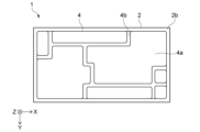
- FIG. 3 is a bottom view showing an example of the ceramic circuit board according to the embodiment.
- the metal member 4 is bonded to the lower surface 2b of the ceramic substrate 2.
- 4a is the lower surface of the metal member.
- 4b is a groove formed in the metal member 4.
- the metal member 4 may be used as a heat sink or may be joined to other parts.
- a metal member 4 having a circuit shape formed on the surface (lower surface 4a) of the metal member 4 may be provided on the lower surface 2b.
- the grooves 4b are formed so that the metal member 4 has the same shape as the plurality of metal circuits 3 shown in FIG.
- the groove 4b is aligned with the gap between the metal circuits 3 in the Z direction. Further, the shape and size of the outer edge of the metal member 4 when viewed from the Z direction are approximately the same as the shape and size of the smallest rectangle surrounding the plurality of metal circuits 3 when viewed from the Z direction.
- the depth (dimension in the Z direction) of the groove 4b is, for example, 0.5 times or more the thickness of the metal member 4.
- the thickness of the metal member is preferably 1.0 mm or more.
- the thickness of the metal member is more preferably 2.0 mm or more, most preferably 3.0 mm or more.
- the effects of the present invention can be obtained by controlling the total volume Vf of the metal circuit 3 and the total volume Vb of the metal member 4. It will be done.
- the present invention is particularly effective when the metal circuit 3 and metal member 4 are thick.
- the thickness of each of the metal circuit 3 and the metal member 4 is preferably 1.0 mm or more.
- the difference between the total volume Vf and the total volume Vb tends to become larger.
- the warpage of the ceramic circuit board 1 tends to increase.
- by controlling the total volume Vf of the metal circuit 3 and the total volume Vb of the metal member 4 warpage of the ceramic circuit board 1 is reduced even when the metal circuit 3 and the metal member 4 are thick. can.
- the upper limit of the thickness of each of the metal circuit 3 and the metal member 4 is not particularly limited, but is preferably 20 mm or less. If the thickness exceeds 20 mm, stress will concentrate at the bonding interface and cracks may occur in the ceramic substrate 2. It may become difficult to make the ceramic substrate 2 thinner in order to suppress the occurrence of cracks.
- the ceramic circuit board 1 includes a ceramic substrate 2, a metal circuit 3, and a metal member 4.
- the metal circuit 3 and the metal member 4 are bonded to the upper surface 2a and lower surface 2b of the ceramic substrate 2, respectively.
- the thickness of the metal circuit 3 and the metal member 4 is 1.0 mm or more.
- Vf/Vb which is the ratio of the total volume Vf of the metal circuit 3 to the total volume Vb of the metal member 4, is preferably 0.80 or more and 1.20 or less.
- a semiconductor element is mounted on the metal circuit 3 of the ceramic circuit board 1. When current flows through a semiconductor element, heat is generated in the semiconductor element. The temperature of the ceramic circuit board 1 increases as the heat generated by the semiconductor element is transferred to the ceramic circuit board 1.
- the ratio Vf/Vb is within the range of 0.80 or more and 1.20 or less, the difference between the thermal expansion of the metal circuit 3 and the thermal expansion of the metal member 4 becomes small.
- the temperature of the ceramic circuit board 1 rises, stress caused by the difference between the thermal expansion of the metal circuit 3 and the thermal expansion of the metal member 4 is alleviated.
- the warpage of the ceramic circuit board 1 is reduced.
- the bonding strength, the board bending strength, and the heat cycle resistance are improved.
- the ratio Vf/Vb is within the range of 0.80 or more and 1.20 or less, and is preferably closer to 1.
- the ratio Vf/Vb is more preferably 0.90 or more and 1.10 or less, and still more preferably 0.95 or more and 1.05 or less.
- the respective thicknesses of the metal circuit 3 and the metal member 4 and the ratio Vf/Vb are controlled.
- a ceramic circuit board 1 with excellent reliability is obtained. be able to.
- FIGS. 4(a) to 4(c) are bottom views showing other examples of the ceramic circuit board according to the embodiment.
- the metal member 4 provided on the lower surface 2b does not have to have a circuit shape. That is, in the example shown in FIG. 4(a), a single plate-shaped metal member 4 is provided on the lower surface 2b of the ceramic substrate 2.
- the total volume Vf of the metal circuits 3 is calculated in advance, and the thickness of the metal member 4 is adjusted so that the ratio Vf/Vb is 0.8. Control is performed so that the value is 1.2 or less.
- a groove may be formed in the metal member 4 to adjust the total volume Vb of the metal member 4.
- 4b indicates a groove formed in the metal member 4.
- lattice-shaped grooves 4b are formed.
- the groove 4b can be formed by cutting, pressing, or etching. By forming the groove 4b in the metal member 4, the total volume Vb of the metal member 4 can be reduced.
- the ratio Vf/Vb can be kept within the range of 0.8 or more and 1.2 or less. can be controlled.
- the heat dissipation of the metal member 4 can be improved by not separating the metal member 4 into a plurality of members and connecting the parts of the metal member 4 at the bottoms of the grooves 4b.
- the total volume Vb can also be adjusted by adjusting the area of the metal member 4 in the XY plane (first surface).
- the ratio Vf/Vb may be controlled within a range of 0.8 or more and 1.2 or less.
- the ratio Af/Ab between the sum of the areas Af of the plurality of metal circuits 3 in the XY plane and the area Ab of the metal member 4 in the XY plane is 0.80 or more and 1.20 or less. It is preferable. More preferably, the ratio Af/Ab is 0.90 or more and 1.10 or less. By controlling the ratio Af/Ab in addition to the ratio Vf/Vb, warpage of the ceramic circuit board can be further reduced.
- Examples of the metal used for the metal circuit 3 and the metal member 4 include copper, copper alloy, aluminum, and aluminum alloy. Copper and copper alloys have high electrical conductivity and are excellent materials for electrical circuits. Copper and copper alloys also have high thermal conductivity and are excellent in heat dissipation of semiconductor elements mounted on metal circuits.
- the metal circuit 3 and the metal member 4 are bonded to the ceramic substrate 2 via the first bonding layer 5a and the second bonding layer 5b, respectively.
- the first bonding layer 5a and the second bonding layer 5b contain at least two selected from the group consisting of silver, copper, titanium, zirconium, hafnium, niobium, tin, indium, zinc, aluminum, silicon, carbon, and magnesium. It is preferable to include.
- the metal circuit 3 and the metal member 4 are made of copper or a copper alloy, it is preferable to provide a bonding layer containing Cu (copper) and Ti (titanium) between the ceramic substrate and each metal circuit.
- the bonding layer containing Cu and Ti is formed using an active metal brazing material.
- Ti is an active metal.
- active metals include Zr (zirconium), Hf (hafnium), and Nb (niobium).
- Active metal brazing materials include mixtures of Ti, Cu, and Ag (silver). For example, the Ti content is 0.1 to 10 wt%, the Cu content is 10 to 60 wt%, and the balance is Ag.
- one or more selected from the group consisting of In (indium), Sn (tin), Al (aluminum), Si (silicon), C (carbon), and Mg (magnesium) can be added in an amount of 1 to 15 wt%. May be added.
- an active metal brazing material paste is applied to the surface of the ceramic substrate 2, and a metal plate is placed thereon. The obtained laminate is heated at 600 to 900° C. to bond the ceramic substrate and metal plate.
- the bonding strength between the ceramic substrate 2 and the metal circuit 3 and the bonding strength between the ceramic substrate 2 and the metal member 4 can be 50 MPa or more.
- the metal circuit 3 and the metal member 4 are made of aluminum or an aluminum alloy, it is preferable to provide a bonding layer containing Al (aluminum) and Si (silicon) between the ceramic substrate and each metal circuit.
- the bonding layer containing Al and Si is formed using an aluminum brazing material.
- the content of Si is 8 to 15 wt%, and the balance is Al.
- one or more selected from the group consisting of In (indium), Sn (tin), Ti (titanium), Cu (copper), Ag (silver), C (carbon), and Mg (magnesium). may be added in an amount of 1 to 15 wt%.
- the brazing joining method using aluminum brazing material an aluminum brazing material paste is applied to the surface of a ceramic substrate, and a metal plate is placed on top of the aluminum brazing material paste.
- the obtained laminate is heated at 500 to 700° C. to bond the ceramic substrate and metal plate.
- the bonding strength between the ceramic substrate 2 and the metal circuit 3 and the bonding strength between the ceramic substrate 2 and the metal member 4 can be 50 MPa or more.
- a metal thin film whose main component is one selected from the group consisting of Ni (nickel), Ag (silver), and Au (gold) may be provided on the surface of the metal circuit 3 or the metal member 4.
- these metal thin films include plating films and sputtering films.
- the ceramic circuit board 1 according to the embodiment is suitable for semiconductor devices.
- a semiconductor element is mounted on a metal circuit with a bonding layer interposed therebetween.
- FIG. 5 is a cross-sectional view showing an example of a semiconductor device according to an embodiment.
- 1 is a ceramic circuit board.
- 6 is a semiconductor device.
- 7 is a semiconductor element.
- 8 is a bonding layer.
- 9 is wire bonding.
- a plurality of metal circuits 3 are bonded to the upper surface 2a of the ceramic substrate 2.
- a semiconductor element 7 is bonded onto one metal circuit 3 via a bonding layer 8 .
- the metal circuit 3 to which the semiconductor element 7 is bonded and another metal circuit 3 are electrically connected by wire bonding 9.
- a metal member 4 is bonded to the lower surface 2b.
- a groove 4b is formed in the metal member 4, and the ratio Vf/Vb is controlled to be 0.80 or more and 1.20 or less.
- the semiconductor device according to the embodiment is not limited to such a structure.
- a plurality of semiconductor elements 7 may be provided on a plurality of metal circuits 3, respectively.
- a plurality of semiconductor elements 7 and a plurality of wire bondings 9 may be provided on one metal circuit 3.
- a semiconductor element and wire bonding may be bonded to the metal member 4 as well, if necessary.
- a metal terminal such as a lead frame may be joined to the metal circuit 3 or the metal member 4.
- solder is preferably lead-free solder.
- Solder refers to a material with a melting point of 450°C or lower.
- Brazing material refers to a material with a melting point of over 450°C.
- a brazing filler metal with a melting point of 500° C. or higher is called a high-temperature brazing filler metal. Examples of high-temperature brazing materials include brazing materials containing Ag as a main component.
- Vf/Vb which is the ratio of the total volume Vf of the metal circuits 3 to the total volume Vb of the metal members 4, is 0.80 or more and 1.20 or less. Therefore, stress generated in the ceramic circuit board 1 can be alleviated. Residual stress is generated in the ceramic circuit board 1 due to the bonding between the ceramic substrate 2 and each metal circuit. Furthermore, semiconductor elements are usually mounted on the metal circuit. Heat generated from the semiconductor element causes a difference in thermal expansion between the ceramic substrate and the metal circuit, generating stress. When the ratio Vf/Vb is 0.80 or more and 1.20 or less, stress generated in the metal circuit becomes small.
- the reliability of the ceramic circuit board can be improved.
- a semiconductor device semiconductor module
- a plurality of semiconductor elements can be mounted on a ceramic circuit board.
- a temperature coefficient indicating a change in electrical resistance with respect to temperature changes from positive to negative. That is, as the temperature rises, the electrical resistance also decreases.
- thermal runaway occurs in which electric power flows intensively, resulting in a phenomenon in which the semiconductor device is destroyed. Therefore, it is very effective to improve the reliability of the bond between the semiconductor element and the metal circuit.
- the semiconductor device according to the embodiment can be used in PCU, IGBT, and IPM modules used in inverters of automobiles (including electric vehicles), electric railway vehicles, industrial machines, air conditioners, and the like.
- automobiles electric vehicles are becoming more popular.
- the reliability of semiconductor devices improves, the safety of automobiles can be improved.
- the manufacturing method of the ceramic circuit board 1 is not particularly limited as long as it has the above-described configuration.
- an example of a method for obtaining the ceramic circuit board 1 with high yield will be given.
- the ceramic substrate 2 is preferably one selected from an aluminum oxide substrate, an aluminum nitride substrate, and a silicon nitride substrate.
- the ceramic substrate 2 is preferably a silicon nitride substrate having a thermal conductivity of 50 W/(m ⁇ K) or more and a three-point bending strength of 600 MPa or more.
- the metal plate is preferably made of one selected from copper and copper alloy.
- a ceramic substrate 2 having a through hole is prepared.
- the through holes may be formed in advance at the stage of forming the molded body.
- a through hole may be formed in the ceramic substrate 2 (ceramic sintered body).
- the through hole is formed by laser processing, cutting, or the like. Examples of the cutting process include drilling using a drill or the like.
- each of the metal circuits 3 molded into a circuit shape is bonded to the upper surface 2a.
- a metal plate calculated from the circuit dimensions is used.
- the thickness of the metal plate joined to the lower surface 2b is preferably adjusted according to the total volume Vf calculated from the circuit dimensions.
- the copper plate or copper alloy plate is preferably bonded to the ceramic substrate 2 by an active metal bonding method.
- an active metal brazing filler metal that is a mixture of an active metal such as Ti and Cu is used.
- active metal brazing materials include mixtures of Ti and Cu, mixtures of Ti, Ag, and Cu, and the like.
- the Ti content is 0.1 to 10 wt%
- the Cu content is 10 to 60 wt%
- the balance is Ag.
- one or more selected from the group consisting of In, Sn, Al, Si, C, and Mg may be added within the range of 1 to 15 wt%.
- the aluminum plate or aluminum alloy plate is preferably joined to the ceramic substrate 2 by an aluminum brazing method.
- an aluminum brazing material is used.
- the aluminum brazing material include a mixture of Al and Si.
- the content of Si is 8 to 15 wt%, and the balance is Al. If necessary, 1 to 15 wt% of one or more selected from the group consisting of In, Sn, Ti, Cu, Ag, C, and Mg may be added.
- the brazing metal is used in the form of a paste.
- the paste is made by mixing a brazing material component and an organic substance.
- the brazing material components are preferably mixed uniformly. If the brazing filler metal components are unevenly distributed, the brazing will not be stable and may cause joint failure.
- a brazing paste is applied to the upper surface 2a and lower surface 2b of the ceramic substrate 2.
- the laminate of the ceramic substrate 2 and the metal plate is heated to bond the ceramic substrate 2 and the metal plate.
- the laminate is heated at 700-900°C.
- aluminum plates or aluminum alloy plates are used, the laminate is heated at 500 to 700°C.
- the heating step is performed in vacuum or in a non-oxidizing atmosphere, if necessary.
- the pressure is preferably 1 ⁇ 10 ⁇ 2 Pa or less.
- the non-oxidizing atmosphere include a nitrogen atmosphere and an argon atmosphere.
- the metal plate When forming the metal circuit 3 by etching, the metal plate is etched and processed into the circuit shape after bonding. After bonding, grooves 4b may be formed in the metal plate (metal member 4) on the lower surface 2b by etching, as shown in FIG. 3, FIG. 4(b), or FIG. 4(c).
- the ceramic circuit board 1 can be manufactured.
- a step of bonding the semiconductor element 7 and the like to the ceramic circuit board 1 is performed.
- a bonding layer 8 is provided at a location where the semiconductor element 7 is bonded.
- Bonding layer 8 preferably contains solder or brazing material.
- a bonding layer 8 is provided, and a semiconductor element 7 is provided thereon.
- Wire bonding 9 is provided as necessary.
- a plurality of semiconductor elements 7 and a plurality of wire bondings 9 may be provided as necessary.
- FIG. 6 is a flowchart illustrating an example of the manufacturing method according to the embodiment.
- FIG. 6 illustrates a case where a metal plate is molded into a circuit shape in advance.
- a ceramic substrate 2 is prepared (step S1). Separately from the ceramic substrate 2, a metal plate is press-molded, cut, or wire-cut to produce a metal circuit 3 (step S2). A brazing paste is applied to both sides of the ceramic substrate 2 (step S3).
- the metal circuit 3 is placed on the top surface 2a of the ceramic substrate 2, and the metal member 4 is placed on the bottom surface 2b (step S4). Heat bonding is performed to bond the metal circuit 3 and the metal member 4 to the ceramic substrate 2 (step S5).
- the ceramic circuit board 1 according to the embodiment is manufactured.
- a bonding layer 8 is formed on the metal circuit 3 of the ceramic circuit board 1 (step S6).
- the semiconductor element 7 is provided on the bonding layer 8, and the semiconductor element 7 is bonded to the metal circuit 3 (step S7).
- the metal circuit 3 is formed by etching, press molding, cutting, wire cutting, or the like. Etching is generally preferred over stamping, machining, or wire cutting.
- press molding it is necessary to prepare a mold corresponding to the shape of the metal circuit 3. Since the mold is expensive, the manufacturing cost of the ceramic circuit board 1 increases. The processing speed of cutting and wire cutting is slow, and cutting and wire cutting are unsuitable for mass production.
- side etching does not occur when forming the metal circuit 3 by press molding, cutting, or wire cutting. Therefore, the total volume Vf of the metal circuit 3 can be easily controlled.
- the metal circuit 3 formed by press molding, cutting, or wire cutting is particularly preferably used.
- By forming the metal circuit 3 by press molding, cutting, or wire cutting it becomes easy to control the ratio Vf/Vb to 0.80 or more and 1.20 or less.
- the volume of the metal plate bonded to the ceramic substrate 2 is controlled. Specifically, the ratio between the total volume Vf0 of the metal circuits 3 (or metal plates) bonded to the upper surface 2a of the ceramic substrate 2 and the total volume Vb0 of the metal members 4 bonded to the lower surface 2b of the ceramic substrate 2. It is preferable that Vf0/Vb0 is 0.80 or more and 1.20 or less.
- the thermal expansion of the metal member 4 provided on the lower surface 2b is larger than the thermal expansion of the metal circuit 3 provided on the upper surface 2a.
- the ceramic substrate 2, the metal circuit 3, and the metal member 4 are joined with the metal member 4 expanded to a greater extent than the metal circuit 3.
- the metal member 4 contracts more than the metal circuit 3.
- the ceramic circuit board 1 warps in a convex shape toward the top surface. If the ratio Vf0/Vb0 is less than 0.80, the stress on the bonded body due to the difference between the thermal expansion of the metal member 4 and the thermal expansion of the metal circuit 3 becomes large, which deteriorates bonding strength, substrate bending strength, and heat cycle resistance. may decrease.
- the thermal expansion of the metal circuit 3 is larger than that of the metal member 4.
- the ceramic circuit board 1 warps in a convex shape toward the lower surface.
- the ratio Vf0/Vb0 is larger than 1.20, stress on the joined body due to the difference between the thermal expansion of the metal member 4 and the thermal expansion of the metal circuit 3 increases. As the stress of the bonded body increases, bonding strength, substrate bending strength, and heat cycle resistance may decrease.
- the ratio Vf0/Vb0 is 0.80 or more and 1.20 or less, stress caused by bonding can be alleviated. Thereby, the bonding strength, substrate bending strength, and heat cycle resistance of the ceramic circuit board 1 can be further improved.
- the ratio Vf0/Vb0 In order to control the ratio Vf0/Vb0, it is effective to join the metal circuit 3 formed by press molding, cutting, or wire cutting to the upper surface 2a.
- the total volume Vf0 of the metal plate at the time of bonding is larger than the total volume Vf of the metal circuit 3 after etching. Therefore, the total volume Vf0 tends to be larger than the total volume Vb0.
- Ceramic substrates shown in Table 1 were prepared.
- the prepared ceramic substrates are a silicon nitride substrate, an aluminum nitride substrate, and an aluminum oxide (alumina) substrate.
- the thermal conductivity of the silicon nitride substrate is 90 W/(m ⁇ K), and the three-point bending strength is 650 MP.
- the aluminum nitride substrate has a thermal conductivity of 170 W/(m ⁇ K) and a three-point bending strength of 300 MPa.
- the thermal conductivity of the aluminum oxide substrate is 20 W/(m ⁇ K), and the three-point bending strength is 350 MPa.
- the size of the ceramic substrate is 30 mm long x 55 mm wide.
- the thickness of the silicon nitride substrate is 0.32 mm and 0.63 mm.
- the thickness of the aluminum nitride substrate and the alumina substrate is 0.63 mm.
- a silicon nitride substrate is written as "Si 3 N 4 ”
- an aluminum nitride substrate is written as "AlN”
- an aluminum oxide substrate is written as "Al 2 O 3 .”
- the thickness T1 (mm) of each ceramic substrate is as shown in Table 1.
- metal plates shown in Table 1 were prepared.
- the metal plate is pre-processed into a predetermined size by press molding.
- the shape of each metal circuit 3 bonded to the upper surface 2a is as shown in FIG. 2.
- a metal member 4 having a shape shown in FIG. 3, FIG. 4(a), FIG. 4(b), or FIG. 4(c) was joined to the lower surface 2b.
- the metal plate is a copper plate or an aluminum plate.
- the copper plate is written as "Cu” and the aluminum plate is written as "Al".
- the thickness T2 (mm) of the metal circuit on the upper surface 2a and the thickness T3 (mm) of the metal member on the lower surface 2b are as shown in Table 1.
- Table 1 describes the processing method from a metal plate to a metal circuit. In the example described as "press molding”, a metal plate is punched out by press molding to form the metal circuit 3. In the example described as “etching,” the metal plate is processed into the metal circuit 3 by etching. In Examples 1 to 7, Examples 9 to 12, Comparative Examples 1 to 3, and Comparative Examples 6 to 7, metal plates with grooves 4b formed by cutting were prepared.
- a brazing material paste was prepared by mixing the raw materials for the brazing material and further mixing an organic component.
- a brazing paste was applied to both sides of the ceramic substrate, and a metal plate or metal circuit was placed on each side.
- the metal plates on the upper surface and the metal plate on the lower surface were arranged so that they faced each other in the Z direction.
- the position, shape, and size of the smallest rectangle surrounding the plurality of metal circuits 3 when viewed from the Z direction are the position of the outer edge of the metal member 4 when viewed from the Z direction, A plurality of metal circuits were placed on the top surface and a metal plate was placed on the bottom surface so as to substantially match the shape and size.
- an active metal brazing filler metal When the material of the metal circuit was copper, an active metal brazing filler metal was used. The content of Ti in the active metal brazing material is 2 wt%, the content of Sn is 10 wt%, the content of Cu is 30 wt%, and the balance is Ag. When the material of the metal circuit was aluminum, an aluminum brazing filler metal was used. The content of Si in the aluminum brazing material is 12 wt%, and the remainder is Al.
- the obtained laminate was subjected to a heating bonding process in vacuum (1 ⁇ 10 ⁇ 2 Pa or less).
- the bonding temperature was set at 820°C.
- the bonding temperature was set at 650°C.
- the bonding time was set to 10 minutes.
- the upper metal plate was etched to form the circuit shape shown in FIG. 2.
- the lower metal plate was etched to form the circuit shape shown in FIG. 3.
- Example 1 to 5 the total volume Vf was determined from the dimensions of the metal circuit 3 after press molding. was calculated.
- Example 6 and Comparative Example 3 the area of the upper base (upper surface 3a) of each metal circuit 3 and the distance between the metal circuits 3 were measured after etching. The distance was measured along the upper surface 2a of the ceramic substrate 2. From this distance, the area of the bottom of the metal circuit 3 was calculated. The shape of each metal circuit 3 was approximated to a truncated quadrangular pyramid, and the total volume Vf was calculated from the area of the upper base, the area of the lower base, and the thickness of the metal circuit 3.
- Example 6 and Comparative Example 3 the area of the upper base of each metal member 4 after etching and the distance between the metal members 4 were measured.
- the shape of each metal member 4 was approximated to a truncated quadrangular pyramid, and the total volume Vb was calculated from the area of the upper base (lower surface 4a), the area of the lower base, and the thickness of the metal member 4.
- Examples 9 and 10 the dimensions of the metal member 4 and the length and depth of the groove 4b were measured, and the total volume Vb was calculated from these values.
- the ratio Vf/Vb was calculated from the total volume Vf and the total volume Vb.
- the amount of warpage of each ceramic circuit board according to Examples and Comparative Examples was measured using a coordinate measuring machine.
- the amount of warpage when the ceramic circuit board follows a convex shape toward the metal circuit 3 is described as a positive value.
- the amount of warpage when the ceramic circuit board follows a convex shape toward the metal member 4 is described as a negative value.
- pull strength was measured as the bonding strength between the circuit and the ceramic substrate. The pull strength was measured by fixing the ceramic circuit board to a jig and peeling off part of the metal circuit in the vertical direction at a rate of 50 mm/min.
- TCT temperature cycle test
- the peeling area due to cracks after 50 cycles was calculated by scanning acoustic tomograph (SAT).
- SAT scanning acoustic tomograph
- the unpeeled area is calculated by subtracting the area of the peeled portion from the total area of the bonded portion.
- the unpeeled area ratio ⁇ was calculated by dividing the unpeeled area by the total area.
- ⁇ 100%
- ⁇ 0%
- Table 2 shows the measurement results of the total volume Vf, total volume Vb, ratio Vf/Vb, amount of warpage, bonding strength, and unpeeled rate.
- the ratio of the total volume Vf of the metal circuits 3 to the total volume Vb of the metal members 4 was within a preferable range.
- these ratios were outside the preferred range. Comparing the results of Examples 1 to 12 with the results of Comparative Examples 1 to 7, the amount of warpage of the ceramic circuit boards of Examples 1 to 12 is greater than the amount of warpage of the ceramic circuit boards of Comparative Examples 1 to 7. small. This is thought to be due to the fact that in the example, the warpage of the ceramic circuit board was suppressed by controlling the ratio Vf/Vb, and in the comparative example, the stress due to the difference in thermal expansion between the metal circuit 3 and the metal member 4 was large.
- the bonding strengths of the ceramic circuit boards according to Examples 1 to 12 are higher than those of the ceramic circuit boards according to Comparative Examples 1 to 7. This is thought to be because the stress in the ceramic substrate 2 and the metal circuit 3 is relaxed, making it difficult for cracks to occur at the bonding interface between the metal circuit 3 and the semiconductor element 7. Further, in Examples 1 to 12, the unpeeled rate was 79% or more, whereas in Comparative Examples 1 to 7, the unpeeled rate was 58% at maximum. Therefore, it can be seen that controlling the ratio Vf/Vb is particularly effective in improving reliability against thermal cycles.
- the metal member 4 has the shapes shown in FIGS. 4(a) to 4(c), respectively. Comparing the results of Examples 8 to 10, when the groove 4b is formed, the difference between the ratio Vf/Vb and "1" is larger than when the groove 4b is not formed. On the other hand, the bonding strength and non-peeling rate have improved. From this result, it can be seen that when the ratio Vf/Vb is approximately the same, providing the groove 4b can improve the bonding strength and the non-peeling rate. This is because the concentration of stress on the lower surface 2b and the metal member 4 can be alleviated by forming the groove 4b.
- Embodiments of the invention include the following features.
- a ceramic substrate a metal circuit with a thickness of 1 mm or more provided on one surface of the ceramic substrate; a metal member with a thickness of 1 mm or more provided on the other surface of the ceramic substrate, A ceramic circuit board, wherein Vf/Vb, which is a ratio between the total volume Vf of the metal circuits and the total volume Vb of the metal members, is 0.80 or more and 1.20 or less.
- Vf/Vb which is a ratio between the total volume Vf of the metal circuits and the total volume Vb of the metal members, is 0.80 or more and 1.20 or less.
- Additional note 3 The ceramic circuit board according to any one of Supplementary Notes 1 to 2, wherein the metal circuit is formed by press molding, cutting, or wire cutting.
- a plurality of the metal circuits are provided on the one surface of the ceramic substrate, The sum Af of the areas of the plurality of metal circuits on a first surface perpendicular to a first direction connecting the one surface and the other surface of the ceramic substrate, and the area Ab of the metal member on the first surface.
- Appendix 5 The ceramic circuit board according to any one of Supplementary notes 1 to 4, wherein each of the metal circuit and the metal member has a thickness of 2 mm or more.
- first bonding layer bonding the ceramic substrate and the metal circuit; further comprising a second bonding layer bonding the ceramic substrate and the metal member,
- first bonding layer and the second bonding layer includes at least two layers selected from the group consisting of silver, copper, titanium, zirconium, hafnium, niobium, tin, indium, zinc, aluminum, silicon, carbon, and magnesium.
- the ceramic circuit board according to appendix 8 comprising: (Appendix 10) A ceramic circuit board according to any one of Supplementary notes 1 to 9, a semiconductor element mounted on the metal circuit via a bonding layer; A semiconductor device equipped with (Appendix 11) A metal circuit is formed by press molding, cutting, or wire cutting on a metal plate, bonding the metal circuit to one side of a ceramic substrate; A method for manufacturing a ceramic circuit board, the method comprising: bonding a metal member to the other surface of the ceramic circuit board; A method for manufacturing a ceramic circuit board, wherein Vf/Vb, which is a ratio between the total volume Vf of the metal circuits and the total volume Vb of the metal members, is 0.80 or more and 1.20 or less.
- Appendix 12 The method for manufacturing a ceramic circuit board according to appendix 11, wherein each of the metal circuit and the metal member has a thickness of 2 mm or more.
- Appendix 13 A method for manufacturing a semiconductor device, comprising mounting a semiconductor element on the metal circuit of a ceramic circuit board manufactured by the manufacturing method described in Appendix 11 or Appendix 12 via a bonding layer.
Landscapes
- Engineering & Computer Science (AREA)
- Microelectronics & Electronic Packaging (AREA)
- Structure Of Printed Boards (AREA)
- Chemical & Material Sciences (AREA)
- Ceramic Engineering (AREA)
- Ceramic Products (AREA)
Priority Applications (4)
| Application Number | Priority Date | Filing Date | Title |
|---|---|---|---|
| CN202380015201.6A CN118402060A (zh) | 2022-04-18 | 2023-04-07 | 陶瓷电路基板、半导体装置、陶瓷电路基板的制造方法以及半导体装置的制造方法 |
| EP23791703.4A EP4513547A4 (en) | 2022-04-18 | 2023-04-07 | CERAMIC CIRCUIT SUBSTRATE, SEMICONDUCTOR DEVICE, METHOD FOR MANUFACTURING CERAMIC CIRCUIT SUBSTRATE AND METHOD FOR MANUFACTURING SEMICONDUCTOR DEVICE |
| JP2024516191A JPWO2023204054A1 (https=) | 2022-04-18 | 2023-04-07 | |
| US18/665,942 US20240304516A1 (en) | 2022-04-18 | 2024-05-16 | Ceramic circuit substrate, semiconductor device, method for manufacturing ceramic circuit substrate, and method for manufacturing semiconductor device |
Applications Claiming Priority (2)
| Application Number | Priority Date | Filing Date | Title |
|---|---|---|---|
| JP2022067982 | 2022-04-18 | ||
| JP2022-067982 | 2022-04-18 |
Related Child Applications (1)
| Application Number | Title | Priority Date | Filing Date |
|---|---|---|---|
| US18/665,942 Continuation US20240304516A1 (en) | 2022-04-18 | 2024-05-16 | Ceramic circuit substrate, semiconductor device, method for manufacturing ceramic circuit substrate, and method for manufacturing semiconductor device |
Publications (1)
| Publication Number | Publication Date |
|---|---|
| WO2023204054A1 true WO2023204054A1 (ja) | 2023-10-26 |
Family
ID=88419910
Family Applications (1)
| Application Number | Title | Priority Date | Filing Date |
|---|---|---|---|
| PCT/JP2023/014392 Ceased WO2023204054A1 (ja) | 2022-04-18 | 2023-04-07 | セラミックス回路基板、半導体装置、セラミックス回路基板の製造方法、及び半導体装置の製造方法 |
Country Status (5)
| Country | Link |
|---|---|
| US (1) | US20240304516A1 (https=) |
| EP (1) | EP4513547A4 (https=) |
| JP (1) | JPWO2023204054A1 (https=) |
| CN (1) | CN118402060A (https=) |
| WO (1) | WO2023204054A1 (https=) |
Citations (4)
| Publication number | Priority date | Publication date | Assignee | Title |
|---|---|---|---|---|
| JPH0786703A (ja) * | 1993-09-10 | 1995-03-31 | Toshiba Corp | セラミックス回路基板 |
| JP4557398B2 (ja) | 2000-09-07 | 2010-10-06 | 株式会社東芝 | 電子素子 |
| JP2013042165A (ja) * | 2005-08-29 | 2013-02-28 | Hitachi Metals Ltd | 回路基板及びこれを用いた半導体モジュール、回路基板の製造方法 |
| JP6430382B2 (ja) | 2013-08-08 | 2018-11-28 | 株式会社東芝 | 回路基板および半導体装置 |
Family Cites Families (2)
| Publication number | Priority date | Publication date | Assignee | Title |
|---|---|---|---|---|
| JP6341822B2 (ja) * | 2014-09-26 | 2018-06-13 | 三菱電機株式会社 | 半導体装置 |
| WO2018021473A1 (ja) * | 2016-07-28 | 2018-02-01 | 株式会社 東芝 | 回路基板および半導体モジュール |
-
2023
- 2023-04-07 JP JP2024516191A patent/JPWO2023204054A1/ja active Pending
- 2023-04-07 WO PCT/JP2023/014392 patent/WO2023204054A1/ja not_active Ceased
- 2023-04-07 EP EP23791703.4A patent/EP4513547A4/en active Pending
- 2023-04-07 CN CN202380015201.6A patent/CN118402060A/zh active Pending
-
2024
- 2024-05-16 US US18/665,942 patent/US20240304516A1/en active Pending
Patent Citations (4)
| Publication number | Priority date | Publication date | Assignee | Title |
|---|---|---|---|---|
| JPH0786703A (ja) * | 1993-09-10 | 1995-03-31 | Toshiba Corp | セラミックス回路基板 |
| JP4557398B2 (ja) | 2000-09-07 | 2010-10-06 | 株式会社東芝 | 電子素子 |
| JP2013042165A (ja) * | 2005-08-29 | 2013-02-28 | Hitachi Metals Ltd | 回路基板及びこれを用いた半導体モジュール、回路基板の製造方法 |
| JP6430382B2 (ja) | 2013-08-08 | 2018-11-28 | 株式会社東芝 | 回路基板および半導体装置 |
Non-Patent Citations (1)
| Title |
|---|
| See also references of EP4513547A4 |
Also Published As
| Publication number | Publication date |
|---|---|
| EP4513547A4 (en) | 2026-04-29 |
| JPWO2023204054A1 (https=) | 2023-10-26 |
| US20240304516A1 (en) | 2024-09-12 |
| EP4513547A1 (en) | 2025-02-26 |
| CN118402060A (zh) | 2024-07-26 |
Similar Documents
| Publication | Publication Date | Title |
|---|---|---|
| JP6359455B2 (ja) | 半導体回路基板およびそれを用いた半導体装置並びに半導体回路基板の製造方法 | |
| CN107534033B (zh) | 接合体、自带散热器的功率模块用基板、散热器及接合体的制造方法、自带散热器的功率模块用基板的制造方法、散热器的制造方法 | |
| CN107534034B (zh) | 接合体、自带散热器的功率模块用基板、散热器及接合体的制造方法、自带散热器的功率模块用基板的制造方法、散热器的制造方法 | |
| KR102154882B1 (ko) | 파워 모듈 | |
| JP7204962B2 (ja) | セラミックス回路基板および半導体モジュール | |
| JP7790968B2 (ja) | セラミックス銅回路基板およびそれを用いた半導体装置 | |
| JP5957862B2 (ja) | パワーモジュール用基板 | |
| WO2013018504A1 (ja) | 半導体装置とその製造方法 | |
| KR20170044105A (ko) | 접합체, 히트 싱크가 부착된 파워 모듈용 기판, 히트 싱크, 접합체의 제조 방법, 히트 싱크가 부착된 파워 모듈용 기판의 제조 방법, 및 히트 싱크의 제조 방법 | |
| JP2014177031A (ja) | 接合体、パワーモジュール用基板、及びヒートシンク付パワーモジュール用基板 | |
| WO2007142261A1 (ja) | パワー素子搭載用基板、その製造方法、パワー素子搭載用ユニット、その製造方法、およびパワーモジュール | |
| WO2003046981A1 (fr) | Structure de module et module comprenant celle-ci | |
| JP6896734B2 (ja) | 回路基板および半導体モジュール | |
| KR20170046649A (ko) | 접합체, 히트 싱크가 부착된 파워 모듈용 기판, 히트 싱크, 접합체의 제조 방법, 히트 싱크가 부착된 파워 모듈용 기판의 제조 방법, 및 히트 싱크의 제조 방법 | |
| JP2016076507A (ja) | パワーモジュール用基板及び冷却器付パワーモジュール用基板の製造方法 | |
| JP2025027018A (ja) | セラミックススクライブ基板、セラミックス基板、セラミックススクライブ基板の製造方法、セラミックス基板の製造方法、セラミックス回路基板の製造方法、及び、半導体素子の製造方法 | |
| JP4104429B2 (ja) | モジュール構造体とそれを用いたモジュール | |
| JP7211949B2 (ja) | セラミックス回路基板 | |
| JP6614256B2 (ja) | 絶縁回路基板 | |
| US20200413534A1 (en) | Insulated circuit board | |
| US20240332123A1 (en) | Scribed ceramic circuit substrate, ceramic circuit substrate, method for producing scribed ceramic circuit substrate, method for producing ceramic circuit substrate, and method for producing semiconductor device | |
| JP2019149460A (ja) | 絶縁回路基板及びその製造方法 | |
| WO2023204054A1 (ja) | セラミックス回路基板、半導体装置、セラミックス回路基板の製造方法、及び半導体装置の製造方法 | |
| JPH08102570A (ja) | セラミックス回路基板 | |
| CN119547203A (zh) | 多层接合体及使用该多层接合体的半导体装置、以及它们的制造方法 |
Legal Events
| Date | Code | Title | Description |
|---|---|---|---|
| 121 | Ep: the epo has been informed by wipo that ep was designated in this application |
Ref document number: 23791703 Country of ref document: EP Kind code of ref document: A1 |
|
| ENP | Entry into the national phase |
Ref document number: 2024516191 Country of ref document: JP Kind code of ref document: A |
|
| WWE | Wipo information: entry into national phase |
Ref document number: 202380015201.6 Country of ref document: CN |
|
| WWE | Wipo information: entry into national phase |
Ref document number: 2023791703 Country of ref document: EP |
|
| NENP | Non-entry into the national phase |
Ref country code: DE |
|
| ENP | Entry into the national phase |
Ref document number: 2023791703 Country of ref document: EP Effective date: 20241118 |