WO2023199569A1 - 電動モータの駆動制御装置 - Google Patents
電動モータの駆動制御装置 Download PDFInfo
- Publication number
- WO2023199569A1 WO2023199569A1 PCT/JP2023/002368 JP2023002368W WO2023199569A1 WO 2023199569 A1 WO2023199569 A1 WO 2023199569A1 JP 2023002368 W JP2023002368 W JP 2023002368W WO 2023199569 A1 WO2023199569 A1 WO 2023199569A1
- Authority
- WO
- WIPO (PCT)
- Prior art keywords
- electric motor
- drive control
- control device
- connector block
- back surface
- Prior art date
- Legal status (The legal status is an assumption and is not a legal conclusion. Google has not performed a legal analysis and makes no representation as to the accuracy of the status listed.)
- Ceased
Links
Images













Classifications
-
- H—ELECTRICITY
- H02—GENERATION; CONVERSION OR DISTRIBUTION OF ELECTRIC POWER
- H02K—DYNAMO-ELECTRIC MACHINES
- H02K11/00—Structural association of dynamo-electric machines with electric components or with devices for shielding, monitoring or protection
- H02K11/30—Structural association with control circuits or drive circuits
- H02K11/33—Drive circuits, e.g. power electronics
-
- H—ELECTRICITY
- H01—ELECTRIC ELEMENTS
- H01R—ELECTRICALLY-CONDUCTIVE CONNECTIONS; STRUCTURAL ASSOCIATIONS OF A PLURALITY OF MUTUALLY-INSULATED ELECTRICAL CONNECTING ELEMENTS; COUPLING DEVICES; CURRENT COLLECTORS
- H01R4/00—Electrically-conductive connections between two or more conductive members in direct contact, i.e. touching one another; Means for effecting or maintaining such contact; Electrically-conductive connections having two or more spaced connecting locations for conductors and using contact members penetrating insulation
- H01R4/02—Soldered or welded connections
- H01R4/028—Soldered or welded connections comprising means for preventing flowing or wicking of solder or flux in parts not desired
-
- H—ELECTRICITY
- H02—GENERATION; CONVERSION OR DISTRIBUTION OF ELECTRIC POWER
- H02K—DYNAMO-ELECTRIC MACHINES
- H02K5/00—Casings; Enclosures; Supports
- H02K5/04—Casings or enclosures characterised by the shape, form or construction thereof
- H02K5/10—Casings or enclosures characterised by the shape, form or construction thereof with arrangements for protection from ingress, e.g. water or fingers
-
- H—ELECTRICITY
- H02—GENERATION; CONVERSION OR DISTRIBUTION OF ELECTRIC POWER
- H02K—DYNAMO-ELECTRIC MACHINES
- H02K5/00—Casings; Enclosures; Supports
- H02K5/04—Casings or enclosures characterised by the shape, form or construction thereof
- H02K5/22—Auxiliary parts of casings not covered by groups H02K5/06-H02K5/20, e.g. shaped to form connection boxes or terminal boxes
- H02K5/225—Terminal boxes or connection arrangements
-
- H—ELECTRICITY
- H05—ELECTRIC TECHNIQUES NOT OTHERWISE PROVIDED FOR
- H05K—PRINTED CIRCUITS; CASINGS OR CONSTRUCTIONAL DETAILS OF ELECTRIC APPARATUS; MANUFACTURE OF ASSEMBLAGES OF ELECTRICAL COMPONENTS
- H05K3/00—Apparatus or processes for manufacturing printed circuits
- H05K3/30—Assembling printed circuits with electric components, e.g. with resistors
- H05K3/32—Assembling printed circuits with electric components, e.g. with resistors electrically connecting electric components or wires to printed circuits
- H05K3/34—Assembling printed circuits with electric components, e.g. with resistors electrically connecting electric components or wires to printed circuits by soldering
- H05K3/3489—Composition of fluxes; Application thereof; Other processes of activating the contact surfaces
-
- H—ELECTRICITY
- H05—ELECTRIC TECHNIQUES NOT OTHERWISE PROVIDED FOR
- H05K—PRINTED CIRCUITS; CASINGS OR CONSTRUCTIONAL DETAILS OF ELECTRIC APPARATUS; MANUFACTURE OF ASSEMBLAGES OF ELECTRICAL COMPONENTS
- H05K2203/00—Indexing scheme relating to apparatus or processes for manufacturing printed circuits covered by H05K3/00
- H05K2203/07—Treatments involving liquids, e.g. plating, rinsing
- H05K2203/0736—Methods for applying liquids, e.g. spraying
Definitions
- the present invention relates to a drive control device for an electric motor, and more particularly to a technique for suppressing dripping of flux applied in a pre-soldering process when mounting a printed circuit board on the back surface of a connector block.
- Patent Document 1 describes a spray-type flux application device for spraying and applying flux to the surface of a printed circuit board when soldering electronic components and the like to the board.
- a spray control member is provided to control the range in which the flux liquid sprayed from the spray nozzle diffuses.
- the present invention was made in view of the above circumstances, and its purpose is to suppress the dripping of flux applied in the pre-soldering process when mounting a printed circuit board to a connector block.
- An object of the present invention is to provide an electric motor drive control device that can reduce manufacturing costs.
- a connector block is provided with a connection opening in which a portion of a terminal member is exposed and the exposed terminal member is connected to a terminal member of a mating connector, and the connector block is coupled to the connector block;
- the connector block includes an exterior member that accommodates and seals a printed circuit board used for drive control of the electric motor, and the connector block is connected to the A drive control for an electric motor, comprising: a soldering terminal portion from which a terminal member protrudes; and a storage portion provided on the back surface for storing excess flux applied to the soldering terminal portion and flowing out.
- Equipment is provided.
- the excess flux storage section is provided, when a printed circuit board is mounted on the connector block, the excess flux applied in the pre-soldering process is stored in the storage section and the connector block is It can prevent it from sagging to the sides. This makes it possible to stably supply high-quality products by suppressing adhesion to the seal portion of the exterior member and transfer from the glove. Furthermore, manufacturing costs can also be reduced by reducing the need for visual confirmation of flux residue and manual wiping.
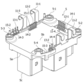
- FIG. 3 is a plan view of the back of a connector block in the electric motor drive control device according to the embodiment of the present invention.
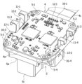
- FIG. 2 is a perspective view of the connector block shown in FIG. 1;
- FIG. 3 is a perspective view for explaining a process of mounting a printed circuit board on the back surface of the connector block shown in FIG. 2;
- 1 is an external perspective view of an electric motor drive control device according to an embodiment of the present invention.
- 5 is an exploded perspective view of the electric motor drive control device shown in FIG. 4.
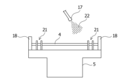
- FIG. FIG. 3 is a front view for explaining a flux application process.
- FIG. 7 is a front view for explaining another example of the flux application process.
- FIG. 7 is an enlarged sectional view for explaining the flow of flux liquid in the soldering terminal portion in the flux application process shown in FIG. 6;
- FIG. 7 is a cross-sectional view for explaining a first modification of the excess flux storage section.
- FIG. 7 is a cross-sectional view for explaining a second modification of the excess flux storage section.
- FIG. 7 is a cross-sectional view for explaining a third modification of the excess flux storage section.
- FIG. 7 is a cross-sectional view for explaining a fourth modification of the excess flux storage section.
- FIG. 7 is a cross-sectional view for explaining a fifth modification of the excess flux storage section.
- FIG. 7 is a cross-sectional view for explaining a sixth modification of the excess flux storage section.
- FIG. 7 is a cross-sectional view for explaining a seventh modification of the excess flux storage section.
- FIG. 7 is a cross-sectional view for explaining an eighth modification of the excess flux storage section.
- FIG. 7 is a cross-sectional view for explaining a ninth modification of the excess flux storage section.
- FIG. 1 is a plan view of the back of the connector block
- FIG. 2 is a perspective view of the connector block seen from the back side
- FIG. 3 is a perspective view for explaining the process of mounting a printed circuit board on the back of the connector block
- 4 is an external perspective view of a drive control device for an electric motor
- FIG. 5 is an exploded perspective view of the drive control device shown in FIG. 4.
- This electric motor drive control device is applied to, for example, an electric steering device of a vehicle, and is used for drive control of an electric motor that generates or assists steering force.
- the electric motor drive control device 10 includes a motor body 2 housed in an exterior member (cover) 1, mounted components 3 for controlling the drive of the motor body 2, and various electronic components.
- the exterior member 1 and the exterior member 6 form a pair and are joined via a sealing material (not shown).
- a motor shaft and a gear 2a attached to the motor shaft protrude from one surface of the exterior member 1, and an opening 6a is formed on the opposing surface of the exterior member 6, which is provided on the front side 5a of the connector block 5.
- the connection opening 5c protrudes.
- the connector block 5 shown in FIGS. 1 and 2 is a molded body in which a portion of a terminal member is sealed.
- the front face 5a of the connector block 5 is provided with a connection opening 5c through which a terminal member is connected to a terminal member of a mating connector.
- thickened collars 5-1 to 5-4 are formed to increase durability and strength.
- sensor input terminals 12-1, 12-2 and CAN communication terminals 13-1, 13-2 are provided on the back surface 5b of this connector block 5.
- the power terminals 11-1 to 11-4 are connected to terminals on the printed circuit board 4 side by TIG welding.
- through holes of the printed circuit board 4 are inserted into the sensor input terminals 12-1, 12-2 and the CAN communication terminals 13-1, 13-2, as shown in FIG. It is a soldering terminal part that is soldered.
- the back surface 5b of the connector block 5 is provided with a recessed portion 14-1 having a rectangular opening.
- a row of sensor input terminals 12-1 is arranged within this recess 14-1 in contact with the long side of the back surface 5b that is away from the peripheral edge.
- the recessed portion 14-1 functions as a storage portion for storing excess flux applied to the sensor input terminal 12-1 and flowing out.
- a barrier portion 15-1 is provided at the peripheral edge of the back surface 5b of the connector block 5 corresponding to the row of sensor input terminals 12-2.
- a recessed portion 14-2 is provided between the barrier portion 15-1 and the sensor input terminal 12-2, in contact with the row of sensor input terminals 12-2. The barrier portion 15-1 and the recessed portion 14-2 form a storage portion for storing excess flux applied to the sensor input terminal 12-2 and flowing out.
- barrier portions 15-2 and 15-3 are provided at the peripheral edge of the connector block rear surface 5b of the CAN communication terminals 13-1 and 13-2.
- Recesses 14-3 and 14-4 are provided between these CAN communication terminals 13-1 and 13-2 and barrier sections 15-2 and 15-3, respectively.
- the barrier part 15-2 and the recessed part 14-3, and the barrier part 15-3 and the recessed part 14-4 each serve as a storage part for storing the excess flux applied to the CAN communication terminals 13-1 and 13-2 and flowing out.
- the sensor input terminal 12-1 located at a distance from the peripheral edge stores excess flux in the recess 14-1.
- the sensor input terminal 12-2 near the peripheral edge is stored in the barrier part 15-1 and the recessed part 14-2.
- the CAN communication terminal 13-1 near the periphery has a barrier portion 15-2 and a recessed portion 14-3
- the CAN communication terminal 13-2 near the periphery has a barrier portion 15-3 and a recessed portion 14-4. The excess flux is stored in each.
- the printed circuit board 4 has a structure in which first and second mounting parts 4a and 4b corresponding to the planar shape of the back surface 5b of the connector block 5 are connected by a flexible part 4c. .
- Semiconductor devices such as FETs and various electronic components are mounted on the first and second mounting sections 4a and 4b.
- the first mounting section 4a is first installed on the back surface 5b of the connector block 5, and the sensor input terminals 12-1, 12-2 and the CAN communication terminal are connected to the through holes of the first mounting section 4a. Insert 13-1 and 13-2.
- the surface of the first mounting portion 4a around these terminals is the area 16-1, 16-2, 16-3, 16-4 where the flux agent is sprayed. After spraying the flux agent, soldering is performed.
- the second mounting section 4b is stacked on the first mounting section 4a, and the printed circuit board 4 is mounted on the back surface 5b of the connector block 5.
- FIG. 6 shows the process of applying flux.
- Flux agent 22 is applied from the spray nozzle 17 to the areas 16-1, 16-2, 16-3, 16-4) surrounded by broken lines around the CAN communication terminals 1, 12-2 and 13-1, 13-2.
- This shows the process of spray coating.
- a girt wall 18 may be provided along the outer periphery of the back surface 5b of the connector block 5, as shown in FIG.
- excess flux flowing out from the sensor input terminal 12-1 (region 16-1) is stored in the storage section formed by the recess 14-1. Further, excess flux flowing out from the sensor input terminal 12-2 portion (region 16-2) is stored in a storage portion made up of the recessed portion 14-2 and the barrier portion 15-1. Similarly, excess flux flowing out from the CAN communication terminal 13-1 portion (region 16-3) is stored in a storage portion consisting of the recessed portion 14-3 and the barrier portion 15-2. Excess flux flowing out from the CAN communication terminal 13-2 portion (area 16-4) is stored in a storage portion consisting of a recessed portion 14-3 and a barrier portion 15-3.
- FIG. 8 shows an enlarged view of the soldering terminal section 21 (sensor input terminals 12-1, 12-2, CAN communication terminals 13-1, 13-2).
- a built-up portion 19 is formed at the base of the soldering terminal portion 21 .
- the built-up portion 19 is formed in a convex shape upward from the back surface 5b of the connector block 5, and the top surface 19a is narrower than the bottom surface 19b. By narrowing the upper surface 19a in this manner, excess flux is easily guided to the recessed portion along the inclined surface 19c, and the amount of flux retained can be reduced.
- the build-up portion 19 can prevent the flux from accumulating at the base of the soldering terminal portion 21 and increase the number of droplets, so that it can prevent the flux from flowing in the form of droplets toward the peripheral edge. Furthermore, the risk of migration due to flux residue entering the interface between the resin of the connector block 5 and the soldering terminal portion 21 can be reduced. Note that by forming an inclined surface or a roundness on the upper surface 19a of the built-up portion 19, the amount of flux retained can be further suppressed.
- FIGS. 9A to 9I are cross-sectional views for explaining various modifications of the excess flux storage section.
- the cross section of the built-up portion 19 is rectangular (the bottom surface and the top surface are the same width) is shown, but it is preferable to have a shape in which the top surface is narrower than the bottom surface as described above, or the built-up portion It is preferable to form a slope or a roundness on the upper surface of 19.
- FIG. 9A shows an example in which the built-up portion 19 is arranged within the recessed portion 14.
- the top surface 19a of the built-up portion 19 is lower than the back surface 5b of the connector block 5, and the upper portion 5d of the outer edge of the connector block 5 is lower than the top surface 19a of the built-up portion 19. Then, the excess flux is stored in the recess 14 up to the upper part 5d of the outer edge of the connector block 5.
- FIG. 9B shows an example in which the built-up portion 19 and the recessed portion 14 are arranged apart from each other.
- the top surface 19a of the built-up part 19 is lower than the back surface 5b of the connector block 5, and the height between the built-up part 19 and the recessed part 14 is the same as the upper part 5d of the outer edge of the connector block 5.
- a separation section 5e is formed. The separating portion 5e and the upper portion 5d of the outer edge portion are lower than the upper surface 19a of the built-up portion 19. Then, the excess flux passes over the separation part 5e and is stored in the recessed part 14 up to the upper part 5d of the outer edge of the connector block 5.
- FIG. 9C shows an example in which the built-up portion 19 is arranged within the recessed portion 14 and the barrier portion 15 is formed at the outer edge of the connector block 5.
- the top surface 19a of the built-up portion 19 is lower than the back surface 5b of the connector block 5, and the barrier portion 15 is higher than the top surface 19a of the built-up portion 19. Then, the excess flux is stored in the recess 14 up to the back surface 5b of the connector block 5.
- FIG. 9D shows an example in which the built-up portion 19 is arranged within the recessed portion 14 and the barrier portion 15 is formed inside the outer edge of the connector block 5.
- the only difference is the position of the barrier part 15, and the other configurations are the same as the example of FIG. 9C, so the same parts are given the same reference numerals and detailed explanation thereof will be omitted.
- FIGS. 9E, 9F, and 9G each show an example in which a groove 20 is further formed in the recessed portion 14 shown in FIG. 9C.
- one end of the groove 20 is formed in contact with the base of the built-up portion 19, and in FIG. 9F, it is formed between the built-up portion 19 and the barrier portion 15.
- FIG. 9G one end of the groove 20 is formed in contact with the base of the barrier portion 15.
- FIG. 9H and 9I each show an example in which the position of the barrier portion 15 is shifted in the configuration shown in FIG. 9E.
- the barrier portion 15 is formed between the groove 20 and the outer edge of the connector block 5, and in FIG. 9I, the barrier portion 15 is formed in contact with one end of the groove 20.
- the same parts are given the same reference numerals and detailed explanation thereof will be omitted.
- various deformations can be considered in the storage section, and excess flux can be stored.
- the excess flux storage section is provided, when mounting a printed circuit board on the back of the connector block, the excess flux applied in the pre-soldering process can be removed. It can be stored in the storage part and prevented from hanging down to the side surface of the connector block. This enables stable supply of high-quality products by suppressing migration caused by flux residue and inhibition of hardening of the seal portion. Furthermore, manufacturing costs can be reduced by reducing the need for visual confirmation of flux residue and manual wiping work.
Landscapes
- Engineering & Computer Science (AREA)
- Microelectronics & Electronic Packaging (AREA)
- Power Engineering (AREA)
- Manufacturing & Machinery (AREA)
- Motor Or Generator Frames (AREA)
Abstract
Description
図1乃至図5はそれぞれ、本発明の実施形態に係る電動モータの駆動制御装置を示している。図1はコネクタブロックの背面の平面図、図2はコネクタブロックを背面側から見た斜視図、図3はコネクタブロックの背面にプリント回路基板を実装する工程について説明するための斜視図である。また、図4は電動モータの駆動制御装置の外観斜視図、図5は図4に示した駆動制御装置の分解斜視図である。
この電動モータの駆動制御装置は、例えば車両の電動ステアリング装置に適用するもので、操舵力を発生あるいはアシストする電動モータの駆動制御に用いられる。
外装部材1と外装部材6はペアをなしており、図示しないシール材を介して接合される。外装部材1の一方の面からモータ軸とこのモータ軸に取り付けられたギヤ2aが突出しており、外装部材6の対向面には開口6aが形成され、コネクタブロック5の正面5a側に設けられた接続間口5cが突出している。
障壁部15-2と窪み部14-3、障壁部15-3と窪み部14-4はそれぞれ、CAN通信端子13-1,13-2に塗布されて流出した過剰フラックスを貯留する貯留部を形成する。
上記塗布工程においては、図7に示すように、コネクタブロック5の背面5bの外周部に沿ったガート壁18を設けても良い。ガート壁18を設けてスプレーノズル17からフラックス剤22を噴霧することで、フラックス剤22の飛散を低減できる。
同様に、CAN通信端子13-1の部分(領域16-3)から流出した過剰フラックスは、窪み部14-3と障壁部15-2からなる貯留部に貯留される。CAN通信端子13-2の部分(領域16-4)から流出した過剰フラックスは、窪み部14-3と障壁部15-3からなる貯留部に貯留される。
なお、肉盛り部19の上面19aに、傾斜面や丸みを形成することで、フラックスの滞留量を更に抑制できる。
上述したように、貯留部には様々な変形が考えられ、過剰フラックスを貯留できる。
これによって、フラックス残渣によるマイグレーションの発生やシール部の硬化阻害を抑えて高品質な製品の安定的供給が可能となる。また、フラックス残渣の目視による確認作業や、手作業による拭き取り作業を低減できることで製造コストを低減できる。
Claims (14)
- 端子部材の一部が露出され、この露出された端子部材が相手側コネクタの端子部材に接続される接続間口を備えるコネクタブロックと、
前記コネクタブロックに結合され、電動モータの駆動制御に使用されるプリント回路基板を収容して封止する外装部材と、を有する電動モータの駆動制御装置において、
前記コネクタブロックは、前記プリント回路基板の収容空間側の背面から前記端子部材が突出した半田付け端子部と、
前記背面に設けられ、前記半田付け端子部に塗布されて流出した過剰フラックスを貯留する貯留部と、を具備することを特徴とする電動モータの駆動制御装置。 - 前記半田付け端子部は、前記プリント回路基板と重なる位置に形成される、ことを特徴とする請求項1に記載の電動モータの駆動制御装置。
- 前記貯留部は、前記半田付け端子部が突出した前記背面の外縁部よりも窪んで形成された窪み部である、ことを特徴とする請求項1に記載の電動モータの駆動制御装置。
- 前記貯留部は、前記半田付け端子部が突出した前記背面の外縁部よりも窪んで形成された窪み部と、前記背面の前記半田付け端子部に対して外縁方向となる位置に立設される障壁部とを有する、ことを特徴とする請求項1に記載の電動モータの駆動制御装置。
- 端子部材の一部が露出され、この露出された端子部材が相手側コネクタの端子部材に接続される接続間口を備えるコネクタブロックと、
前記コネクタブロックに結合され、電動モータの駆動制御に使用されるプリント回路基板を収容して封止する外装部材と、を有する電動モータの駆動制御装置において、
前記コネクタブロックは、前記プリント回路基板の収容空間側の背面から前記端子部材が突出した半田付け端子部と、
前記背面の前記半田付け端子部における外縁側に、前記背面の外縁部よりも低い窪み部と、を具備することを特徴とする電動モータの駆動制御装置。 - 前記半田付け端子部の根元に設けられた肉盛り部を更に備える、ことを特徴とする請求項5に記載の電動モータの駆動制御装置。
- 前記肉盛り部の傾斜部が、前記窪み部に接続される、ことを特徴とする請求項6に記載の電動モータの駆動制御装置。
- 前記半田付け端子部が、前記窪み部内に設けられる、ことを特徴とする請求項5に記載の電動モータの駆動制御装置。
- 前記窪み部が、前記半田付け端子部と最短距離にある前記コネクタブロックの外縁部の方向に配置される、ことを特徴とする請求項5に記載の電動モータの駆動制御装置。
- 前記窪み部が、前記半田付け端子部と分離され、前記半田付け端子部とコネクタブロックの外縁部との間に配置される、ことを特徴とする請求項5に記載の電動モータの駆動制御装置。
- 前記窪み部は、前記コネクタブロックの取り付け固定位置と前記半田付け端子部との間に延設される、ことを特徴とする請求項5に記載の電動モータの駆動制御装置。
- 端子部材の一部が露出され、この露出された端子部材が相手側コネクタの端子部材に接続される接続間口を備えるコネクタブロックと、
前記コネクタブロックに結合され、電動モータの駆動制御に使用されるプリント回路基板を収容して封止する外装部材と、を有する電動モータの駆動制御装置において、
前記コネクタブロックは、前記プリント回路基板の収容空間側の背面から前記端子部材が突出した半田付け端子部と、
前記背面の前記半田付け端子部における外縁側に、前記背面から突出して設けられた障壁部と、を具備することを特徴とする電動モータの駆動制御装置。 - 前記障壁部が、前記コネクタブロックの取り付け固定位置と前記半田付け端子部との間に延設される、ことを特徴とする請求項12に記載の電動モータの駆動制御装置。
- 前記障壁部と前記半田付け端子部との間に、前記背面の外縁部よりも低い窪み部を更に備える、ことを特徴とする請求項13に記載の電動モータの駆動制御装置。
Priority Applications (3)
| Application Number | Priority Date | Filing Date | Title |
|---|---|---|---|
| CN202380016064.8A CN118525421A (zh) | 2022-04-13 | 2023-01-26 | 电动马达的驱动控制装置 |
| US18/838,715 US20250158494A1 (en) | 2022-04-13 | 2023-01-26 | Electric-motor drive control device |
| JP2024514808A JP7652985B2 (ja) | 2022-04-13 | 2023-01-26 | 電動モータの駆動制御装置 |
Applications Claiming Priority (2)
| Application Number | Priority Date | Filing Date | Title |
|---|---|---|---|
| JP2022-066215 | 2022-04-13 | ||
| JP2022066215 | 2022-04-13 |
Publications (1)
| Publication Number | Publication Date |
|---|---|
| WO2023199569A1 true WO2023199569A1 (ja) | 2023-10-19 |
Family
ID=88329570
Family Applications (1)
| Application Number | Title | Priority Date | Filing Date |
|---|---|---|---|
| PCT/JP2023/002368 Ceased WO2023199569A1 (ja) | 2022-04-13 | 2023-01-26 | 電動モータの駆動制御装置 |
Country Status (4)
| Country | Link |
|---|---|
| US (1) | US20250158494A1 (ja) |
| JP (1) | JP7652985B2 (ja) |
| CN (1) | CN118525421A (ja) |
| WO (1) | WO2023199569A1 (ja) |
Citations (5)
| Publication number | Priority date | Publication date | Assignee | Title |
|---|---|---|---|---|
| JPH0613740A (ja) * | 1992-06-25 | 1994-01-21 | Mitsubishi Electric Corp | プリント配線板 |
| JP2000067963A (ja) * | 1998-08-20 | 2000-03-03 | Jst Mfg Co Ltd | 基板表面実装用コネクタ |
| JP2002319443A (ja) * | 2001-04-20 | 2002-10-31 | Jst Mfg Co Ltd | 電気コネクタ |
| JP2006129692A (ja) * | 2004-09-28 | 2006-05-18 | Mabuchi Motor Co Ltd | 小型モータの光学式エンコーダ装置及びその製造方法 |
| JP2019216604A (ja) * | 2014-07-31 | 2019-12-19 | 株式会社デンソー | 駆動装置、および、これを用いた電動パワーステアリング装置 |
Family Cites Families (1)
| Publication number | Priority date | Publication date | Assignee | Title |
|---|---|---|---|---|
| JPH0413740A (ja) * | 1990-05-08 | 1992-01-17 | Asahi Fiber Glass Co Ltd | 熱可塑性樹脂用混入材並びに樹脂成形体 |
-
2023
- 2023-01-26 WO PCT/JP2023/002368 patent/WO2023199569A1/ja not_active Ceased
- 2023-01-26 CN CN202380016064.8A patent/CN118525421A/zh active Pending
- 2023-01-26 US US18/838,715 patent/US20250158494A1/en active Pending
- 2023-01-26 JP JP2024514808A patent/JP7652985B2/ja active Active
Patent Citations (5)
| Publication number | Priority date | Publication date | Assignee | Title |
|---|---|---|---|---|
| JPH0613740A (ja) * | 1992-06-25 | 1994-01-21 | Mitsubishi Electric Corp | プリント配線板 |
| JP2000067963A (ja) * | 1998-08-20 | 2000-03-03 | Jst Mfg Co Ltd | 基板表面実装用コネクタ |
| JP2002319443A (ja) * | 2001-04-20 | 2002-10-31 | Jst Mfg Co Ltd | 電気コネクタ |
| JP2006129692A (ja) * | 2004-09-28 | 2006-05-18 | Mabuchi Motor Co Ltd | 小型モータの光学式エンコーダ装置及びその製造方法 |
| JP2019216604A (ja) * | 2014-07-31 | 2019-12-19 | 株式会社デンソー | 駆動装置、および、これを用いた電動パワーステアリング装置 |
Also Published As
| Publication number | Publication date |
|---|---|
| US20250158494A1 (en) | 2025-05-15 |
| CN118525421A (zh) | 2024-08-20 |
| JP7652985B2 (ja) | 2025-03-27 |
| JPWO2023199569A1 (ja) | 2023-10-19 |
Similar Documents
| Publication | Publication Date | Title |
|---|---|---|
| KR100510220B1 (ko) | 회로 기판 장치 및 그 실장 방법 | |
| JP4867280B2 (ja) | コーティング剤塗布方法 | |
| US7677905B2 (en) | Electronic device and manufacturing method of the same | |
| CN102833970B (zh) | 电控单元 | |
| CN1930931B (zh) | 控制设备 | |
| US20040223304A1 (en) | Distribution unit and electric connection box including the same | |
| US8701971B2 (en) | Printed board and bus bar assembly | |
| US20100002403A1 (en) | Standardized electronics housing having modular contact partners | |
| US7931478B2 (en) | Electrical junction box | |
| DE102011085170A1 (de) | Steuermodul mit verklebter Trägerplatte | |
| US6927347B2 (en) | Printed circuit board having through-hole protected by barrier and method of manufacturing the same | |
| JP2010258360A (ja) | 箱形電子モジュール | |
| JP7591641B2 (ja) | 電子制御装置 | |
| WO2019012898A1 (ja) | 電子制御装置および電子制御装置の製造方法 | |
| JP7652985B2 (ja) | 電動モータの駆動制御装置 | |
| JP4143280B2 (ja) | 実装構造体、該実装構造体の製造方法、印刷用マスク、および印刷方法 | |
| CN100544561C (zh) | 电子设备及其制造方法 | |
| CN115380635B (zh) | 电子控制装置 | |
| TWI653655B (zh) | Relay | |
| GB2317272A (en) | Electronic part with terminal flux trap | |
| JP2009158586A (ja) | 高周波回路ユニット | |
| JPH04336490A (ja) | リフローハンダの形成方法 | |
| JP4716183B2 (ja) | プリント配線基板及び電気機器 | |
| JP2011134689A (ja) | 車両用自動変速機に設けられる電子回路ユニット | |
| JP7163819B2 (ja) | 半導体モジュール |
Legal Events
| Date | Code | Title | Description |
|---|---|---|---|
| 121 | Ep: the epo has been informed by wipo that ep was designated in this application |
Ref document number: 23787992 Country of ref document: EP Kind code of ref document: A1 |
|
| ENP | Entry into the national phase |
Ref document number: 2024514808 Country of ref document: JP Kind code of ref document: A |
|
| WWE | Wipo information: entry into national phase |
Ref document number: 202380016064.8 Country of ref document: CN |
|
| WWE | Wipo information: entry into national phase |
Ref document number: 18838715 Country of ref document: US |
|
| NENP | Non-entry into the national phase |
Ref country code: DE |
|
| 122 | Ep: pct application non-entry in european phase |
Ref document number: 23787992 Country of ref document: EP Kind code of ref document: A1 |
|
| WWP | Wipo information: published in national office |
Ref document number: 18838715 Country of ref document: US |