WO2023190845A1 - 銅箔及び遮光材 - Google Patents
銅箔及び遮光材 Download PDFInfo
- Publication number
- WO2023190845A1 WO2023190845A1 PCT/JP2023/013130 JP2023013130W WO2023190845A1 WO 2023190845 A1 WO2023190845 A1 WO 2023190845A1 JP 2023013130 W JP2023013130 W JP 2023013130W WO 2023190845 A1 WO2023190845 A1 WO 2023190845A1
- Authority
- WO
- WIPO (PCT)
- Prior art keywords
- copper foil
- less
- rough surface
- coating film
- shielding material
- Prior art date
- Legal status (The legal status is an assumption and is not a legal conclusion. Google has not performed a legal analysis and makes no representation as to the accuracy of the status listed.)
- Ceased
Links
Images
Classifications
-
- C—CHEMISTRY; METALLURGY
- C25—ELECTROLYTIC OR ELECTROPHORETIC PROCESSES; APPARATUS THEREFOR
- C25D—PROCESSES FOR THE ELECTROLYTIC OR ELECTROPHORETIC PRODUCTION OF COATINGS; ELECTROFORMING; APPARATUS THEREFOR
- C25D5/00—Electroplating characterised by the process; Pretreatment or after-treatment of workpieces
- C25D5/10—Electroplating with more than one layer of the same or of different metals
- C25D5/12—Electroplating with more than one layer of the same or of different metals at least one layer being of nickel or chromium
-
- B—PERFORMING OPERATIONS; TRANSPORTING
- B32—LAYERED PRODUCTS
- B32B—LAYERED PRODUCTS, i.e. PRODUCTS BUILT-UP OF STRATA OF FLAT OR NON-FLAT, e.g. CELLULAR OR HONEYCOMB, FORM
- B32B15/00—Layered products comprising a layer of metal
- B32B15/01—Layered products comprising a layer of metal all layers being exclusively metallic
-
- C—CHEMISTRY; METALLURGY
- C23—COATING METALLIC MATERIAL; COATING MATERIAL WITH METALLIC MATERIAL; CHEMICAL SURFACE TREATMENT; DIFFUSION TREATMENT OF METALLIC MATERIAL; COATING BY VACUUM EVAPORATION, BY SPUTTERING, BY ION IMPLANTATION OR BY CHEMICAL VAPOUR DEPOSITION, IN GENERAL; INHIBITING CORROSION OF METALLIC MATERIAL OR INCRUSTATION IN GENERAL
- C23F—NON-MECHANICAL REMOVAL OF METALLIC MATERIAL FROM SURFACE; INHIBITING CORROSION OF METALLIC MATERIAL OR INCRUSTATION IN GENERAL; MULTI-STEP PROCESSES FOR SURFACE TREATMENT OF METALLIC MATERIAL INVOLVING AT LEAST ONE PROCESS PROVIDED FOR IN CLASS C23 AND AT LEAST ONE PROCESS COVERED BY SUBCLASS C21D OR C22F OR CLASS C25
- C23F1/00—Etching metallic material by chemical means
- C23F1/10—Etching compositions
- C23F1/14—Aqueous compositions
- C23F1/16—Acidic compositions
- C23F1/18—Acidic compositions for etching copper or alloys thereof
-
- C—CHEMISTRY; METALLURGY
- C25—ELECTROLYTIC OR ELECTROPHORETIC PROCESSES; APPARATUS THEREFOR
- C25D—PROCESSES FOR THE ELECTROLYTIC OR ELECTROPHORETIC PRODUCTION OF COATINGS; ELECTROFORMING; APPARATUS THEREFOR
- C25D1/00—Electroforming
- C25D1/04—Wires; Strips; Foils
-
- C—CHEMISTRY; METALLURGY
- C25—ELECTROLYTIC OR ELECTROPHORETIC PROCESSES; APPARATUS THEREFOR
- C25D—PROCESSES FOR THE ELECTROLYTIC OR ELECTROPHORETIC PRODUCTION OF COATINGS; ELECTROFORMING; APPARATUS THEREFOR
- C25D5/00—Electroplating characterised by the process; Pretreatment or after-treatment of workpieces
- C25D5/34—Pretreatment of metallic surfaces to be electroplated
-
- C—CHEMISTRY; METALLURGY
- C25—ELECTROLYTIC OR ELECTROPHORETIC PROCESSES; APPARATUS THEREFOR
- C25D—PROCESSES FOR THE ELECTROLYTIC OR ELECTROPHORETIC PRODUCTION OF COATINGS; ELECTROFORMING; APPARATUS THEREFOR
- C25D5/00—Electroplating characterised by the process; Pretreatment or after-treatment of workpieces
- C25D5/48—After-treatment of electroplated surfaces
-
- C—CHEMISTRY; METALLURGY
- C25—ELECTROLYTIC OR ELECTROPHORETIC PROCESSES; APPARATUS THEREFOR
- C25D—PROCESSES FOR THE ELECTROLYTIC OR ELECTROPHORETIC PRODUCTION OF COATINGS; ELECTROFORMING; APPARATUS THEREFOR
- C25D7/00—Electroplating characterised by the article coated
- C25D7/06—Wires; Strips; Foils
- C25D7/0614—Strips or foils
-
- G—PHYSICS
- G02—OPTICS
- G02B—OPTICAL ELEMENTS, SYSTEMS OR APPARATUS
- G02B5/00—Optical elements other than lenses
Definitions
- the present invention relates to copper foil and light shielding materials.
- Light-shielding materials which are members with light-shielding properties, are used in optical devices such as cameras and projectors.
- Examples of light shielding materials include resin light shielding materials (for example, see Patent Document 1) in which a black coating film containing carbon black is formed on a film-like resin base material (for example, a polyethylene terephthalate film);
- a metal light-shielding material is known in which a black coating film containing black is formed on a foil-shaped metal base material (for example, copper foil).
- metal foils copper foils made of copper alone or copper alloys have superior conductivity compared to other metal foils, are less likely to generate static electricity, and can be made into foils with sufficient industrial productivity using electrolysis or rolling methods. Therefore, it is suitable as a base material for light-shielding materials because it has characteristics such as excellent economic efficiency and excellent corrosion resistance.
- conventional copper foils have had the problem of low adhesion to coating films as described above.
- An object of the present invention is to provide a copper foil that has high adhesion to a coating film.
- Another object of the present invention is to provide a light-shielding material that not only has excellent light-shielding properties but also has high adhesion between a black coating film and a base material.
- the present inventors focused on the surface shape of copper foil.
- the surface shape of general copper foil includes a pyramid-like uneven shape formed by plating, a glossy smooth shape, and a polished shape that is a transfer of the polished surface of the plating base material. Either of these shapes.
- rolled copper foil it is a rolled shape including rolling marks and oil pits.
- the surface of the copper foil having the above-mentioned surface shape may be subjected to a plating treatment called roughening treatment to form particles made of copper alone or a copper alloy on the surface of the copper foil.
- the copper foil having the above-mentioned surface shape could not be said to have sufficiently high adhesion with a coating film such as a black coating film.
- a coating film such as a black coating film.
- the solvent of the coating solution used when forming a black coating film on copper foil for example, methyl ethyl ketone, toluene, acetone, butyl acetate
- the resin contained in the coating liquid for example, acrylic resin, polyurethane resin, polyester resin
- the unevenness is fine. This is believed to be because the resin that has entered the gap is easily broken, making it difficult to obtain a sufficient anchoring effect.
- the copper foil according to one embodiment of the present invention has a rough surface having an arithmetic mean curvature Spc of 1300 mm -1 or more and 5000 mm -1 or less and a root mean square slope Sdq of 2° or more and 25° or less. or on both surfaces.
- a light shielding material according to another aspect of the present invention includes a base material made of the copper foil according to the above-mentioned one aspect, and a black coating film formed on the rough surface of the two surfaces of the copper foil. , and has an optical density of 6 or more.
- the copper foil according to the present invention has high adhesion to the coating film. Furthermore, the light shielding material according to the present invention not only has excellent light shielding properties but also has high adhesion between the black coating film and the base material.
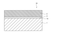
- FIG. 1 is a schematic cross-sectional view illustrating a light shielding material according to an embodiment of the present invention.
- the copper foil 1 according to the present embodiment has a rough surface 1a having an apex arithmetic mean curvature Spc of 1300 mm -1 or more and 5000 mm -1 or less and a root mean square slope Sdq of 2° or more and 25° or less.
- FIG. 1 is an example in which only one surface has a rough surface 1a).
- a rust preventive layer 3 made of nickel (Ni) alone or a nickel alloy and having a thickness of 0.2 nm or more and 300 nm or less may or may not be formed.
- FIG. 1 is an example in which the anticorrosive layer 3 is formed).
- the light shielding material 10 according to the present embodiment includes a base material made of copper foil 1, and a black color formed on the surface having the rough surface 1a of the two surfaces of the copper foil 1. coating film 2, and has an optical density of 6 or more.
- the copper foil 1 according to the present embodiment has the rough surface 1a with the above configuration, it has high adhesion to a coating film containing resin (for example, a black coating film used for a light shielding material). Specifically, if the shape of the unevenness formed on the rough surface of the copper foil is excessively sharp and the sharp unevenness is densely formed, the resin that gets into the narrow gaps between the unevenness easily breaks. Otherwise, there is a risk that a sufficient anchor effect may not be obtained.
- the rough surface 1a of the copper foil 1 according to the present embodiment is a rough surface in which the shape of the formed unevenness is not too sharp and the sharp unevenness is uniformly formed. The resin that has entered is difficult to break, and a sufficient anchoring effect can be obtained. Therefore, it has high adhesion to the coating film.
- the black coating film included in the light shielding material is soft and brittle because it contains a large amount of filler such as carbon black. Therefore, the resin that has entered the narrow gaps between the unevenness formed on the rough surface of the copper foil is likely to break.
- the copper foil 1 according to the present embodiment has the rough surface 1a having the above structure, even if the coating film formed on the surface is a black coating film containing a large amount of filler such as carbon black, Also, the resin that gets into the narrow gaps between the unevenness is difficult to break and a sufficient anchoring effect can be obtained. Therefore, the copper foil 1 according to this embodiment has high adhesion to the black coating film.
- the copper foil 1 according to the present embodiment is suitable as a base material for a light shielding material. That is, the light shielding material 10 according to the present embodiment uses the copper foil 1 having the rough surface 1a having the above structure as a base material, and the black coating film 2 is formed on the surface having the rough surface 1a, so that the light shielding material 10 has a black color. Adhesion between the coating film 2 and the copper foil 1 is high. Further, when the black coating film 2 is formed by coating the coating liquid on the copper foil 1, appearance defects called spots and cissing are less likely to occur. Furthermore, even if the light shielding material 10 is deformed by an external force applied thereto during use, the black coating film 2 is difficult to peel off from the copper foil 1. Furthermore, since the light shielding material 10 according to the present embodiment has an optical density of 6 or more, it has excellent light shielding properties.
- the light shielding material 10 according to the present embodiment can be used as an internal member of an optical device such as a camera or a projector (for example, a member that constitutes the inner wall surface of a camera), a spacer, a shutter, an aperture member, or a ring. It is suitable as a light-shielding material for optical equipment used in, etc.
- An optical device including the light shielding material 10 according to this embodiment is less likely to cause halation or ghosting due to external light.
- the light shielding material 10 according to the present embodiment has excellent light shielding properties even when the copper foil 1 is made thinner, and can be made thinner and lighter, so it is suitable for mobile optical equipment.
- the copper foil 1 and the light shielding material 10 according to this embodiment will be explained in more detail.
- the copper foil 1 according to the present embodiment has a rough surface 1a formed by roughening one or both of the two surfaces of the raw material copper foil, and It can be manufactured by setting the arithmetic mean curvature Spc of 1,300 mm -1 to 5,000 mm -1 and the root mean square slope Sdq of 2° to 25°.
- the type of surface roughening treatment is not particularly limited, but examples include etching treatment, oxidation treatment, redox treatment, mechanical treatment, and plating treatment.
- the etching process is a process in which the surface of the raw copper foil is roughened by contacting the surface with an etching solution and etching it.
- the oxidation treatment is a treatment in which the surface of the raw copper foil is roughened by oxidizing the surface using a gaseous, liquid, or solid oxidizing agent.
- the redox treatment is a treatment in which the surface of raw copper foil is roughened by oxidizing and then reducing the surface.
- Mechanical treatment is a process of roughening the surface of the raw material copper foil by subjecting it to mechanical processing such as sandblasting.
- the plating process is a process of roughening the surface of the raw copper foil by applying plating to form metal particles on the surface of the raw material copper foil.
- micro-etching solution examples include a micro-etching solution consisting of a mixture of sulfuric acid and hydrogen peroxide, and a commercially available micro-etching solution such as MEC Etch Bond CZ-8101, a micro-etching agent manufactured by MEC Co., Ltd. can be mentioned.
- the micro-etching process can be performed by bringing a micro-etching solution into contact with the surface of the raw material copper foil and etching it.
- the method of bringing the micro-etching solution into contact with the surface of the raw copper foil is not particularly limited, but methods include immersion in the micro-etching solution, spraying the micro-etching solution, showering the micro-etching solution, etc. Can be mentioned.
- the time (etching time) for which the surface of the raw material copper foil is brought into contact with the micro-etching solution is not particularly limited, but is preferably 3 seconds or more and 60 seconds or less.
- micro-etching is performed by immersing the raw copper foil in a micro-etching solution, it is preferable to perform the micro-etching while applying ultrasonic vibrations using an ultrasonic generator or the like. Ultrasonic vibrations may be applied over the entire etching time, or may be applied only for a portion of the etching time.
- the output of the ultrasonic vibration is preferably 20 kHz or more and 250 kHz or less. If the output is 20 kHz or more, the micro-etching solution is sufficiently transported to the etching interface, so that the shape of the formed unevenness is not too sharp, and a rough surface with uniformly formed sharp unevenness is easily formed. . Further, if the output is 250 kHz or less, mechanical damage due to ultrasonic vibration is less likely to be applied to the raw copper foil, and the equipment load is likely to be practical.
- the most preferred method is to perform the micro-etching treatment while applying ultrasonic vibration using a micro-etching solution consisting of a mixed solution of sulfuric acid and hydrogen peroxide. According to such micro-etching treatment, the surface of the raw material copper foil can be appropriately roughened.
- the reaction product of the micro-etching solution has a high concentration, it will generally affect the etching rate, so the etching rate will change over time at each uneven location during the micro-etching process.
- the etching shape becomes complicated, the shape of the unevenness formed on the rough surface of the copper foil becomes excessively sharp, and the sharp unevenness is formed in a dense manner.
- the micro-etching solution near the etching interface is rapidly sent far from the etching interface due to cavitation and vibration effects, and micro-etching of the bulk composition is carried out from far away from the etching interface.
- a liquid is delivered near the etching interface. Therefore, it is difficult for the etching rate to change over time at each location of the unevenness. As a result, a rough surface is formed in which the shape of the formed unevenness is not too sharp and the sharp unevenness is uniformly formed.
- the ten-point average roughness Rzjis of the surface of the raw copper foil before roughening treatment is 2 ⁇ m or less.
- This ten-point average roughness Rzjis can be measured using a contact surface roughness measuring machine according to the method specified in JIS B0601:2001. If the ten-point average roughness Rzjis of the surface is 2 ⁇ m or less, the copper foil 1 with high adhesion to the coating film can be easily obtained by the surface roughening treatment.
- the thickness of the raw copper foil before roughening treatment varies depending on the target value of the thickness of the copper foil 1 according to the present embodiment (i.e., the raw copper foil after roughening treatment), but it is 5 ⁇ m or more and 20 ⁇ m or less. It is preferably 5 ⁇ m or more and 18 ⁇ m or less, and even more preferably 6 ⁇ m or more and 18 ⁇ m or less.
- the thickness of the copper foil 1 according to the present embodiment is preferably 5 ⁇ m or more and 18 ⁇ m or less, more preferably 5 ⁇ m or more and 12 ⁇ m or less, and 5. More preferably, the thickness is 5 ⁇ m or more and 12 ⁇ m or less. If the copper foil 1 with a thickness of 5 ⁇ m or more is used as a base material, a light shielding material 10 having sufficient mechanical properties can be obtained. Moreover, if the copper foil 1 with a thickness of 18 ⁇ m or less is used as a base material, a sufficiently thin light shielding material 10 can be obtained.
- the arithmetic mean curvature Spc of the peak of the rough surface 1a of the copper foil 1 must be from 1300 mm -1 to 5000 mm -1 , and from 1400 mm -1 to 5000 mm -1 . It is preferably 1400 mm -1 or more and 4500 mm -1 or less.
- the root mean square slope Sdq of the rough surface 1a of the copper foil 1 must be 2° or more and 25° or less, preferably 3° or more and 25° or less, and 3° or more and 22° or less. is more preferable.
- the arithmetic mean height Sa of the rough surface 1a of the copper foil 1 is preferably 0.03 ⁇ m or more and 0.35 ⁇ m or less, more preferably 0.03 ⁇ m or more and 0.15 ⁇ m or less, and 0.03 ⁇ m or more. More preferably, it is 0.13 ⁇ m or less. When the arithmetic mean height Sa of the rough surface 1a of the copper foil 1 is within the above range, appearance defects are less likely to occur during coating.
- the ten-point average roughness Rzjis of the rough surface 1a of the copper foil 1 is preferably 0.5 ⁇ m or more and 2 ⁇ m or less, more preferably 0.6 ⁇ m or more and 2.0 ⁇ m or less, and 0.6 ⁇ m or more and 1 More preferably, it is .8 ⁇ m or less.
- the lightness L * of the rough surface 1a of the copper foil 1 is preferably 60 or more and 85 or less, more preferably 65 or more and 85 or less.
- appearance defects are less likely to occur during coating, and higher heat resistance is likely to be obtained.
- a rust prevention layer 3 made of nickel alone or a nickel alloy and having a thickness of 0.2 nm or more and 300 nm or less is formed. Good too. If the rust prevention layer 3 is formed, rust formation on the rough surface 1a of the copper foil 1 is suppressed. In addition, since the thickness of the rust prevention layer 3 is thin, the influence of the formation of the rust prevention layer 3 on the arithmetic mean curvature Spc, root mean square slope Sdq, lightness L *, etc. of the peak of the rough surface 1a is small, and the influence of the formation of the rust prevention layer 3 on the peak peak peak peak The arithmetic mean curvature Spc, root mean square slope Sdq, brightness L * , etc. can be sufficiently controlled.
- the type of nickel alloy is not particularly limited, but examples include phosphorus (P), zinc (Zn), silicon (Si), chromium (Cr), iron (Fe), and copper (Cu). Examples include nickel alloys containing at least one element selected from the following.
- the method of forming the anticorrosion layer 3 is not particularly limited, but an example is a plating method.
- the thickness of the anticorrosion layer 3 is not particularly limited, but is preferably 0.2 nm or more and 300 nm or less, more preferably 0.2 nm or more and 40 nm or less, and 0.2 nm or more and 10 nm or less. It is even more preferable. If the thickness of the anticorrosion layer 3 is 0.2 nm or more, the adhesion with the coating film will be higher. Moreover, if the thickness of the anticorrosion layer 3 is 300 nm or less, the influence on the surface shape of the rough surface 1a can be reduced.
- the thickness of the rust prevention layer 3 is 40 nm or less, the curling phenomenon of the copper foil due to the internal stress of the rust prevention layer 3 will be suppressed, and handling during manufacturing and processing of the copper foil will be facilitated. It is possible to reduce machining defects during processing. Furthermore, if the thickness of the anticorrosion layer 3 is 10 nm or less, curling hardly occurs, so processing defects caused by curling can be reduced, and the impact on productivity and cost is also small.
- the coating film is a film containing resin, and contains a resin solution formed by dissolving the resin in a solvent on the surface having the rough surface 1a of the two surfaces of the copper foil 1. It can be formed by applying a coating liquid.
- a black coating film 2 is formed as a coating film on the surface having the rough surface 1a among the two surfaces of the copper foil 1. By using a coating liquid containing a black pigment such as carbon black, a black coating film 2 can be obtained.
- the type of resin contained in the coating film is not particularly limited, but examples include acrylic resins, hydrocarbon resins (e.g., polyester resins, polybutadiene resins), vinyl resins, epoxy resins, and phenolic resins. , melamine resin, urea resin, isocyanate resin, etc. These resins may be used alone or in combination of two or more.
- the type of solvent used in the coating solution is not particularly limited, but examples include ketone solvents such as methyl ethyl ketone and cyclohexanone, ester solvents such as ethyl acetate and methyl acetate, and alcohols such as methanol and ethanol. , toluene, water, etc. These solvents may be used alone or in combination of two or more.
- the optical density of the light shielding material 10 according to the present embodiment needs to be 6 or more, preferably 7 or more, and more preferably 8 or more. If the optical density is 6 or more, the light blocking property of the light blocking material 10 is excellent.
- a coating liquid is applied to the surface having the rough surface 1a of the two surfaces of the copper foil 1 to form the black coating film 2. An example of a method for forming the black coating film 2 will be explained.
- carbon black is dispersed in a resin solution in which the resin is dissolved in a solvent to prepare a coating liquid.
- This coating liquid is applied onto the surface having the rough surface 1a of the two surfaces of the copper foil 1 to form a film of the coating liquid on the surface of the copper foil 1.
- the solvent contained in the coating liquid film is volatilized by heat treatment or the like to form a black coating film 2 on the surface having the rough surface 1a of the two surfaces of the copper foil 1.
- Example ⁇ The present invention will be explained in more detail by showing Examples and Comparative Examples below.
- the Rzjis of the electrolytic deposition finished surface (matte surface) of this electrolytic copper foil is within the range of 0.8 to 1.4 ⁇ m
- the Rzjis of the electrolytic deposition starting surface is within the range of 0.7 to 1.6 ⁇ m.
- the tensile strength of this electrolytic copper foil in a normal state is 320 MPa.
- the matte surface or shiny surface of the electrolytic copper foil was subjected to surface roughening treatment and nickel plating (formation of a rust prevention layer), which will be described later, to obtain a base material.
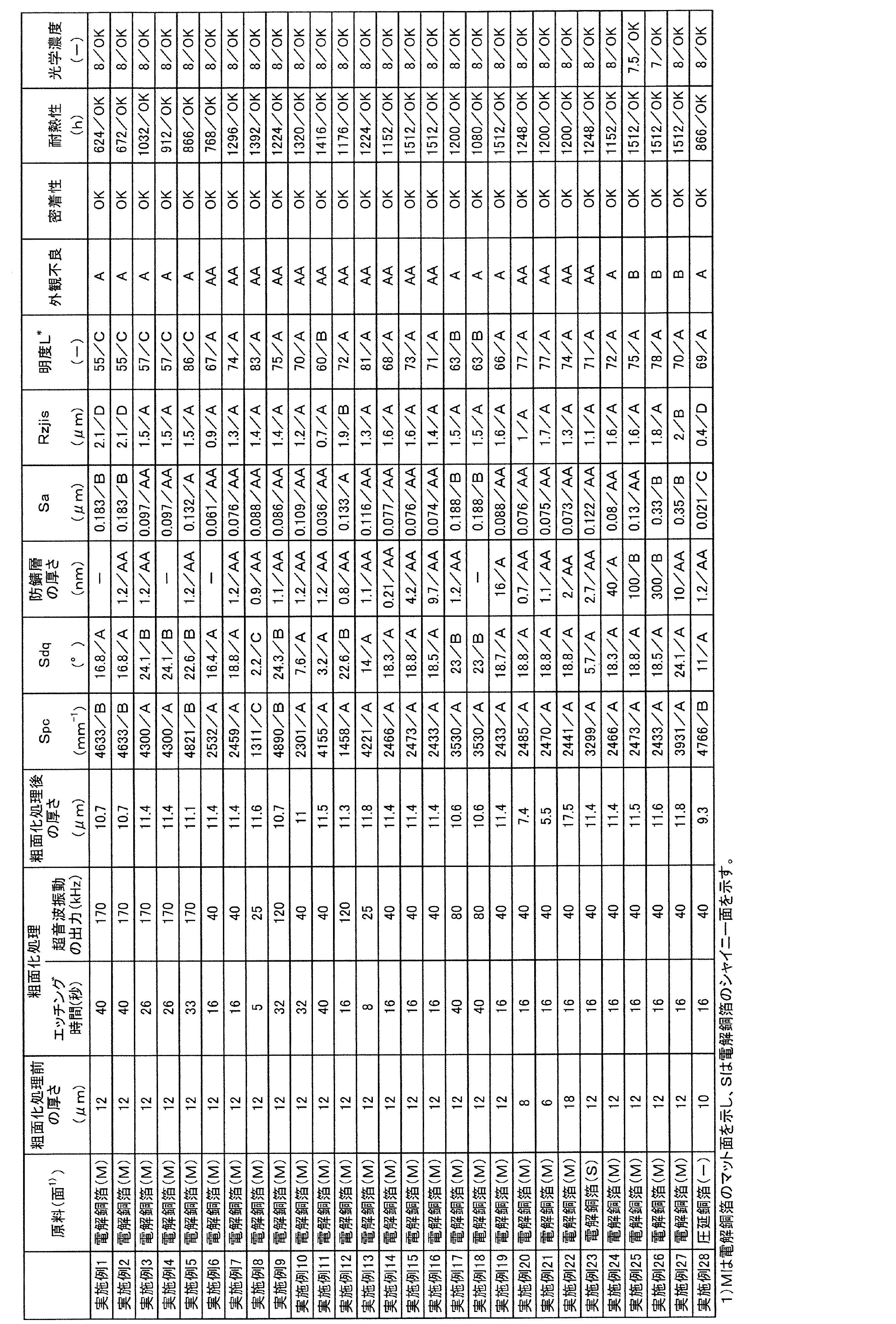
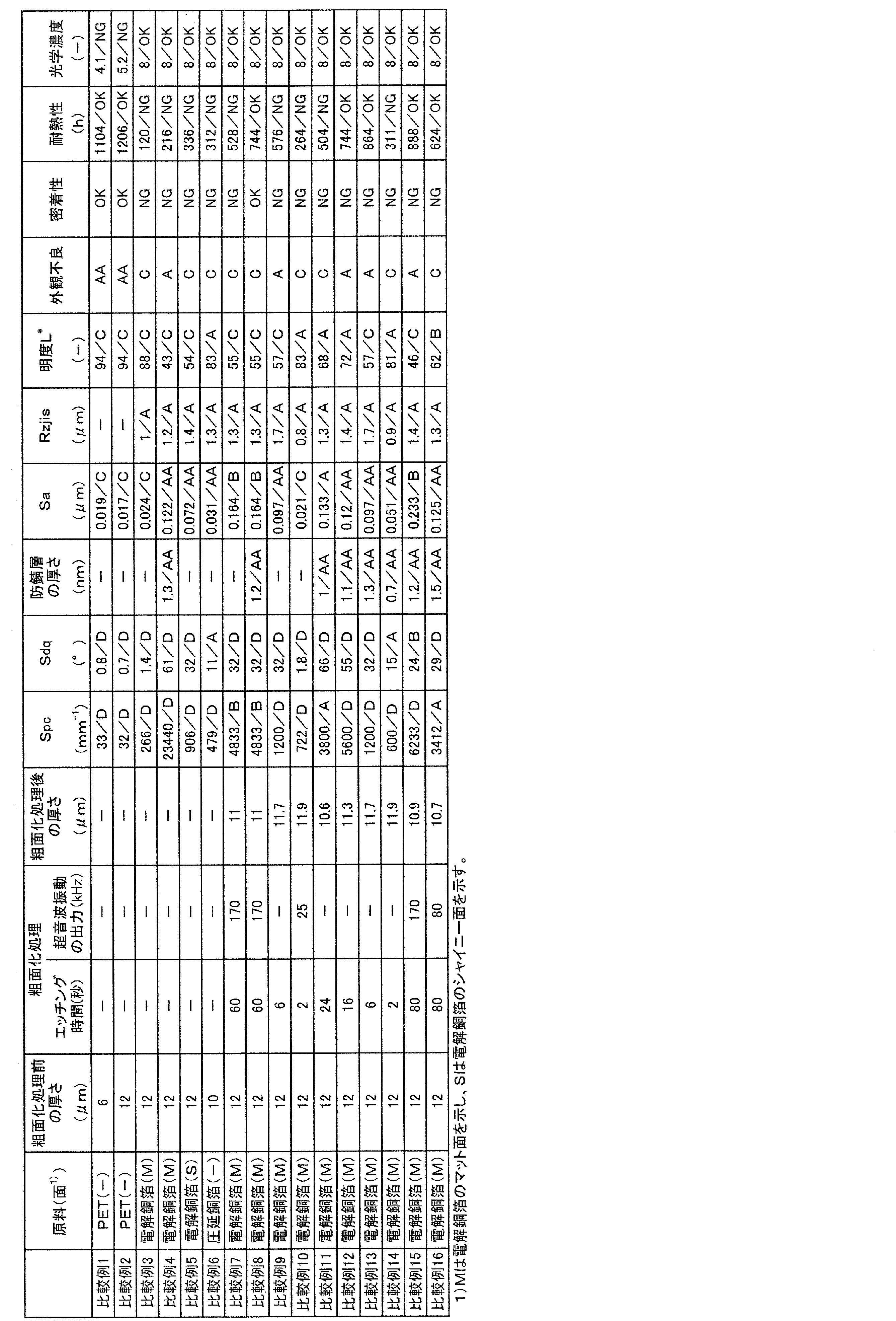
- the roughened and nickel-plated surfaces are as shown in the raw material columns of Tables 1 and 2. However, in Examples 1, 4, 6, and 18 and Comparative Examples 7, 9, and 10, only surface roughening treatment was performed, and nickel plating was not performed.
- a rolled copper foil with a thickness of 10 ⁇ m was prepared as a raw material copper foil that is a raw material for producing the base materials of Example 28 and Comparative Example 6.
- the Rzjis on both sides of this rolled copper foil is within the range of 0.3 to 1.0 ⁇ m.
- the tensile strength of this rolled copper foil in a normal state is 380 MPa.
- one surface of the rolled copper foil was subjected to surface roughening treatment and nickel plating, which will be described later, to form a base material.
- Comparative Example 6 the surface roughening treatment and nickel plating were not performed, and the rolled copper foil was used as the base material.
- Biaxially stretched polyethylene terephthalate (PET) films having the thicknesses shown in Tables 1 and 2 were prepared as resin films that are raw materials for producing the base materials of Comparative Examples 1 and 2.
- the tensile strength of this polyethylene terephthalate film under normal conditions is 205 MPa.
- the polyethylene terephthalate film was used as the base material without roughening treatment or nickel plating.
- Comparative Example 3 the raw material copper foil used in Example 6 was used as a base material without being subjected to surface roughening treatment or nickel plating.
- the black coating film described below was formed on the matte surface.
- electrolytic copper foil F2-WS for printed wiring boards manufactured by Furukawa Electric Co., Ltd. was used as the base material.
- the matte surface of this electrolytic copper foil is plated to form copper particles to give the surface an uneven surface, and then a rust-preventive layer made of zinc, chromium, etc. is applied. is applied.
- the black coating film described below was formed on the matte surface.
- electrolytic copper foil F2-WS for printed wiring boards manufactured by Furukawa Electric Co., Ltd. was used as the base material.
- the shiny surface of this electrolytic copper foil is plated with a rust preventive layer made of zinc, chromium, or the like.
- Example 1 to 28 and Comparative Examples 7, 8, 10, 15, and 16 microetching was performed while applying ultrasonic vibration using an ultrasonic generator.
- the output of ultrasonic vibration is as shown in Tables 1 and 2.
- Comparative Example 9 and Comparative Examples 11 to 14 the micro-etching treatment was performed without applying ultrasonic vibration. Note that the thickness of the copper foil after the surface roughening treatment is shown in Tables 1 and 2.
- the numerical values of the thickness of the rust prevention layer are listed, and if the thickness of the rust prevention layer is 0.2 nm or more and 10 nm or less, it is "AA", and if it is more than 10 nm and 40 nm or less, it is rated “AA”. "A” is used when the thickness exceeds 40 nm and 300 nm or less, and “C” is used when the thickness is less than 0.2 nm or exceeds 300 nm.
- the conditions for nickel plating are as follows.
- Nickel plating conditions Concentration of nickel in plating bath: 40g/L Concentration of boric acid (H 3 BO 3 ) in the plating bath: 5 g/L Concentration of sodium hypophosphite (NaH 2 PO 2 ) in the plating bath: 12 g/L Plating bath temperature: 25°C Plating bath pH: 3.5 Current density: 0.5A/dm 2 Energizing time: 1.5 to 350 seconds
- the characteristics to be evaluated are the ten-point average roughness Rzjis, the arithmetic average height Sa, the arithmetic average curvature Spc of the peak, the root mean square slope Sdq, and the lightness L * .
- a method for evaluating these characteristics will be explained below.
- ⁇ Ten point average roughness Rzjis> The ten-point average roughness Rzjis was measured using a contact surface roughness measuring machine according to the method specified in JIS B0601:2001. The results are shown in Tables 1 and 2.
- the numerical values shown in Tables 1 and 2 are the average values of the measured values at three arbitrary points.
- the values of the ten-point average roughness Rzjis are listed, and if the ten-point average roughness Rzjis is 0.6 ⁇ m or more and 1.8 ⁇ m or less, it is “A”, and if it exceeds 1.8 ⁇ m, it is “A”. If it is 0 ⁇ m or less, it is marked “B”, if it is 0.5 ⁇ m or more and less than 0.6 ⁇ m, it is marked “C”, and if it is less than 0.5 ⁇ m or more than 2.0 ⁇ m, it is marked “D”.
- the arithmetic mean height Sa, arithmetic mean curvature Spc of the peak, and root mean square slope Sdq were measured according to ISO25178 using confocal laser microscopes VK-X1050 and VK-X1000 manufactured by Keyence Corporation. The results are shown in Tables 1 and 2.
- the objective lens magnification of the confocal laser microscope is 100x
- the scan mode is laser confocal
- the measurement size is 2048 x 1536
- the measurement quality is High Precision
- the pitch is 0.08 ⁇ m.
- the numerical values shown in Tables 1 and 2 are the average values of the measured values at three arbitrary points for each of Sa, Spc, and Sdq.
- the numerical value of the arithmetic mean height Sa is written, and if the arithmetic mean height Sa is 0.03 ⁇ m or more and 0.13 ⁇ m or less, it is “AA”, and it is more than 0.13 ⁇ m and 0.15 ⁇ m or less. If it is more than 0.15 ⁇ m, it is written as “B”, and if it is less than 0.03 ⁇ m or more than 0.35 ⁇ m, it is written as “C”.
- the numerical value of the arithmetic mean curvature Spc of the peak is recorded, and if the arithmetic mean curvature Spc of the peak is 1400 mm -1 or more and 4500 mm -1 or less, it is "A”, and if it exceeds 4500 mm -1 If it is 5000 mm -1 or less, it is marked “B”, if it is 1300 mm -1 or more and less than 1400 mm -1 , it is marked “C”, and if it is less than 1300 mm -1 or more than 5000 mm -1 , it is marked "D".
- the lightness L * was measured using an ultraviolet-visible spectrophotometer V-660 (integrating sphere unit) manufactured by JASCO Corporation. Specifically, the total light spectral reflectance at a wavelength of 870 to 200 nm was measured, and the lightness L * was calculated from the spectrum using the software attached to the ultraviolet-visible spectrophotometer. The results are shown in Tables 1 and 2. The numerical values shown in Tables 1 and 2 are the average values of the measured values at three arbitrary points.
- (E) Formation of black coating film A coating liquid was applied to the surface of the substrates of Examples 1 to 28 and Comparative Examples 1 to 16 to form a black coating film on the surface of the substrate, and a light shielding material was applied. Created. In detail, by coating the surface of the base material with a coating liquid using the bar coating method to form a film of the coating liquid, and sufficiently volatilizing the solvent contained in the film of the coating liquid in dry air. , a black coating film was formed. The thickness of the coating liquid before drying was adjusted so that the thickness of the black coating film after drying was 2 ⁇ m.
- a black coating film was formed on the surface that had been subjected to the roughening treatment.
- a black coating film was formed on the surface (matte surface or shiny surface) of the side listed in the raw material column of Table 2.
- the surface on which the black coating film is formed may be on either side.
- composition of the coating liquid is as follows. ⁇ Acrylic polyol (Acrydic A801P manufactured by DIC Corporation (solid content 50% by mass)): 12.2 parts by mass ⁇ Isocyanate (Burnock DN980 manufactured by DIC Corporation (solid content 75% by mass)): 8.5 parts by mass ⁇ Carbon black (Vulcan XC-72 manufactured by Cabot): 6.0 parts by mass ⁇ Methyl ethyl ketone: 42.1 parts by mass ⁇ Toluene: 16.2 parts by mass
- the shape of the bullet or repellent is an irregular shape different from a circular or similar shape, the bullet or repellent whose shape does not fit within a circle with a diameter of 100 ⁇ m is included in the number of bullets or repellent with a diameter of 100 ⁇ m or more. .
- a spot is a part where voids such as air bubbles exist at the interface between the black paint film and the base or inside the black paint film, and the shape of the part is often circular or similar.
- the size is minute.
- a repellent is a recess or hole (a recess that reaches the base material) formed in a part of the black coating film, and the planar shape of the recess and hole is often circular or similar.
- Tables 1 and 2 The evaluation results for poor appearance are shown in Tables 1 and 2.
- Tables 1 and 2 if the total number of particles and repellents with a diameter of 100 ⁇ m or more existing in the evaluation area is 0, "AA”, if the number is 1 or more and 4 or less, "A”, If there are 5 or more and 6 or less, it is marked “B”, and if there are 7 or more, it is marked "C”. Cases where the evaluation is AA, A, and B are considered to be passed, and cases where the evaluation is C are judged to be failed.
- optical density The optical density of the light shielding material was measured using an optical densitometer DD8-N manufactured by Optirius Co., Ltd. The measurement wavelength range was 435-700 nm, and the optical density measurement range was 0-8. The results are shown in Tables 1 and 2. In addition, if the optical density is 6.5 or more, it is considered to be passed and marked as "OK” in Tables 1 and 2, and if it is less than 6.5, it is marked as failed, and in Tables 1 and 2, it is marked as "NG”. I wrote it down. Moreover, the numerical values shown in Tables 1 and 2 are the average values of the measured values at three arbitrary points.
- the copper foils of Examples 1 to 28 have an arithmetic mean curvature Spc of 1300 mm -1 or more and 5000 mm -1 or less at the peak, and a root mean square slope Sdq of 2° or more and 25° or less, so these copper foils can be used as base materials.
- the light-shielding material used as the sample exhibited good appearance, adhesion, and heat resistance, and also exhibited high optical density.
- Comparative Examples 1 and 2 Since the light shielding materials of Comparative Examples 1 and 2 used polyethylene terephthalate film as the base material, as can be seen from Table 2, they exhibited good appearance, adhesion, and heat resistance, but the optical density was poor. That was enough. Further, from the comparison between Comparative Example 1 and Comparative Example 2, it can be seen that the smaller the thickness of the base material, the lower the optical density. Further, from a comparison between Comparative Example 2 and Example 1, it can be seen that even though the thickness of the base material is the same, Comparative Example 2 has a lower optical density.
- the light-shielding materials of Comparative Examples 3 to 6 use copper foil that has not been subjected to surface roughening treatment as a base material, as can be seen from Table 2, the arithmetic mean curvature Spc and root mean square slope Sdq of the peak peaks is outside the above numerical range. Therefore, as can be seen from Table 2, at least one of appearance, adhesion, and heat resistance was poor.
- the light-shielding materials of Comparative Examples 7 to 16 use roughened copper foil as the base material, the arithmetic mean curvature Spc or root mean square slope Sdq of the peak peaks is outside the above numerical range. There is. Therefore, as can be seen from Table 2, at least one of appearance, adhesion, and heat resistance was poor.
Landscapes
- Chemical & Material Sciences (AREA)
- Metallurgy (AREA)
- Materials Engineering (AREA)
- Organic Chemistry (AREA)
- Engineering & Computer Science (AREA)
- Chemical Kinetics & Catalysis (AREA)
- Electrochemistry (AREA)
- Physics & Mathematics (AREA)
- Mechanical Engineering (AREA)
- General Chemical & Material Sciences (AREA)
- Optics & Photonics (AREA)
- General Physics & Mathematics (AREA)
- Laminated Bodies (AREA)
- Electroplating Methods And Accessories (AREA)
- ing And Chemical Polishing (AREA)
- Paints Or Removers (AREA)
Abstract
Description
本発明は、塗膜との密着性が高い銅箔を提供することを課題とする。また、本発明は、優れた遮光性を有することに加えて黒色塗膜と基材との密着性が高い遮光材を提供することを併せて課題とする。
本発明者らは、これらの知見を基に鋭意研究を行った結果、特定の粗面を表面に有することにより、塗膜との密着性が高い銅箔が得られることを見出し、本発明を完成するに至った。
また、本発明の別の態様に係る遮光材は、上記一態様に係る銅箔からなる基材と、銅箔の2つの表面のうち粗面を有する表面の上に形成された黒色塗膜と、を有し、光学濃度が6以上であることを要旨とする。
また、本実施形態に係る遮光材10は、図1に示すように、銅箔1からなる基材と、銅箔1の2つの表面のうち粗面1aを有する表面の上に形成された黒色塗膜2と、を有し、光学濃度が6以上である。
(1)銅箔の製造方法について
本実施形態に係る銅箔1は、原料銅箔が有する2つの表面のうち一方又は両方の表面に粗面化処理を施して粗面1aを設け、山頂点の算術平均曲率Spcを1300mm-1以上5000mm-1以下とするとともに二乗平均平方根傾斜Sdqを2°以上25°以下とすることによって製造することができる。
銅箔1の粗面1aの山頂点の算術平均曲率Spcは、1300mm-1以上5000mm-1以下である必要があり、1400mm-1以上5000mm-1以下であることが好ましく、1400mm-1以上4500mm-1以下であることがより好ましい。
さらに、銅箔1の粗面1aの算術平均高さSaは、0.03μm以上0.35μm以下であることが好ましく、0.03μm以上0.15μm以下であることがより好ましく、0.03μm以上0.13μm以下であることがさらに好ましい。銅箔1の粗面1aの算術平均高さSaが上記範囲内であると、塗膜塗工時の外観不良が発生しにくい。
さらに、銅箔1の粗面1aの明度L*は、60以上85以下であることが好ましく、65以上85以下であることがより好ましい。銅箔1の粗面1aの明度L*が上記範囲内であると、塗膜塗工時の外観不良が発生しにくく、より高い耐熱性が得られやすい。
銅箔1の粗面1aを有する表面の上には、ニッケル単体又はニッケル合金からなり且つ厚さが0.2nm以上300nm以下である防錆層3が形成されていてもよい。防錆層3が形成されていれば、銅箔1の粗面1aの発錆が抑制される。なお、防錆層3の厚さは薄いので、防錆層3の形成による粗面1aの山頂点の算術平均曲率Spc、二乗平均平方根傾斜Sdq、明度L*等への影響は小さく、山頂点の算術平均曲率Spc、二乗平均平方根傾斜Sdq、明度L*等は十分に制御可能である。
防錆層3の形成方法は特に限定されるものではないが、例としてはめっき法が挙げられる。
塗膜は、樹脂を含有する膜であり、銅箔1の2つの表面のうち粗面1aを有する表面の上に、樹脂が溶剤に溶解してなる樹脂溶液を含有する塗工液を塗工することによって形成することができる。本実施形態に係る遮光材10においては、銅箔1の2つの表面のうち粗面1aを有する表面の上に、塗膜として黒色塗膜2が形成されている。カーボンブラック等の黒色顔料が配合された塗工液を用いることにより、塗膜を黒色塗膜2とすることができる。
本実施形態に係る遮光材10の光学濃度は、6以上である必要があり、7以上であることが好ましく、8以上であることがより好ましい。光学濃度が6以上であれば、遮光材10の遮光性が優れている。
本実施形態に係る遮光材10を製造する際には、銅箔1の2つの表面のうち粗面1aを有する表面の上に塗工液を塗工して、黒色塗膜2を形成する。黒色塗膜2を形成する方法の一例を説明する。
以下に実施例及び比較例を示して、本発明をさらに具体的に説明する。
(A)基材
実施例1~28及び比較例7~16の基材を製造するための原料である原料銅箔として、表1、2に示す厚さを有する電解銅箔(両面光沢箔)を用意した。この電解銅箔の電解析出終了面(マット面)のRzjisは0.8~1.4μmの範囲内であり、電解析出開始面(シャイニー面)のRzjisは0.7~1.6μmの範囲内である。また、この電解銅箔の常態における引張強度は320MPaである。
比較例4については、古河電気工業株式会社製のプリント配線板用電解銅箔F2-WSをそのまま基材とした。ただし、この電解銅箔のマット面には、銅からなる粒子を形成して表面に凹凸を付与するめっき処理が施された後に、亜鉛、クロム等で形成された防錆層を設ける防錆めっきが施されている。後述する黒色塗膜は、マット面に形成した。
実施例1~28及び比較例7~16については、銅箔をマイクロエッチング液に浸漬するマイクロエッチング処理により、銅箔の表面に粗面化処理を施した。マイクロエッチング液としては、メック株式会社製のマイクロエッチング剤であるメックエッチボンドCZ-8101を用いた。マイクロエッチング処理の際のマイクロエッチング液の温度は、30℃とした。マイクロエッチング処理を施す時間(エッチング時間)は、表1、2に記載のとおりである。
なお、粗面化処理後の銅箔の厚さを表1、2に示す。
粗面化処理に続いて、実施例2、3、5、実施例7~17、実施例19~28、比較例8、及び比較例11~16については、粗面化処理を施した表面(粗面)に対してニッケルめっきを施すことにより、粗面上に防錆層を形成した。実施例1、4、6、18及び比較例7、9、10については、前述したようにニッケルめっきは施していない。防錆層の厚さは、表1、2に記載のとおりである。なお、表1、2には、防錆層の厚さの数値を記すと共に、防錆層の厚さが0.2nm以上10nm以下である場合は「AA」、10nm超過40nm以下である場合は「A」、40nm超過300nm以下である場合は「B」、0.2nm未満又は300nm超過である場合は「C」と記してある。また、ニッケルめっきの条件は、下記のとおりである。
めっき浴中のニッケルの濃度:40g/L
めっき浴中のホウ酸(H3BO3)の濃度:5g/L
めっき浴中の次亜リン酸ナトリウム(NaH2PO2)の濃度:12g/L
めっき浴の温度:25℃
めっき浴のpH:3.5
電流密度:0.5A/dm2
通電時間:1.5~350秒
粗面化処理を施した銅箔については、粗面化処理を施した側の表面の特性を評価した。粗面化処理を施していない比較例3~5の銅箔については、表2の原料の欄に記載した側の表面(マット面又はシャイニー面)の特性を評価した。比較例1、2、6については、特性を評価する表面は、いずれの側の表面でも差し支えない。
<十点平均粗さRzjis>
十点平均粗さRzjisは、JIS B0601:2001に規定された方法に従って、接触式表面粗さ測定機を用いて測定した。結果を表1、2に示す。表1、2に示した数値は、任意の3点の測定値の平均値である。なお、表1、2には、十点平均粗さRzjisの数値を記すと共に、十点平均粗さRzjisが0.6μm以上1.8μm以下である場合は「A」、1.8μm超過2.0μm以下である場合は「B」、0.5μm以上0.6μm未満である場合は「C」、0.5μm未満又は2.0μm超過である場合は「D」と記してある。
算術平均高さSa、山頂点の算術平均曲率Spc、二乗平均平方根傾斜Sdqは、株式会社キーエンス製の共焦点レーザー顕微鏡VK-X1050及びVK-X1000を用いて、ISO25178に従って測定した。結果を表1、2に示す。
画像処理:平滑化処理、3×3、メディアン
Sフィルター:無し
F-operation:平面傾き補正
Lフィルター:0.025μm
演算対象面積:100μm×100μm
なお、ニッケルめっき層の厚さについては、蛍光X線分光分析を用いて測定した。検量線を用いて銅箔単位面積当たりのニッケル付着質量を測定し、ニッケルの密度8.90g/cm3で除することによって、厚さを算出した。
明度L*は、日本分光株式会社製の紫外可視分光光度計V-660(積分球ユニット)を用いて測定した。詳述すると、波長870~200nmの間での全光線分光反射率を測定し、そのスペクトルから、上記紫外可視分光光度計に付属のソフトウェアを用いて明度L*を算出した。結果を表1、2に示す。表1、2に示した数値は、任意の3点の測定値の平均値である。なお、表1、2には、明度L*の数値を記すと共に、明度L*が65以上85以下である場合は「A」、60以上65未満である場合は「B」、60未満又は85超過である場合は「C」と記してある。
実施例1~28及び比較例1~16の基材の表面に塗工液を塗工して、基材の表面上に黒色塗膜を形成し、遮光材を作製した。詳述すると、基材の表面にバーコート法によって塗工液を塗工して塗工液の膜を形成し、塗工液の膜が含有する溶剤を乾燥空気中で十分に揮発させることによって、黒色塗膜を形成した。乾燥後の黒色塗膜の厚さが2μmになるように、乾燥前の塗工液の膜の厚さを調整した。
・アクリルポリオール(DIC株式会社製のアクリディックA801P(固形分50質量%)):12.2質量部
・イソシアネート(DIC株式会社製のバーノックDN980(固形分75質量%)):8.5質量部
・カーボンブラック(キャボット社製のバルカンXC-72):6.0質量部
・メチルエチルケトン:42.1質量部
・トルエン:16.2質量部
上記のようにして得られた実施例1~28及び比較例1~16の遮光材について、以下の評価を行った。
<外観不良>
黒色塗膜の表面のうち一部の領域を評価領域と定め、該評価領域における外観不良の有無を確認した。すなわち、評価領域に存在する直径100μm以上のブツ及びハジキの合計の個数を計測した。評価領域は、縦200mm、横150mmの長方形状の領域であり、その縦方向は塗工液の塗工時に塗工液を流延した方向である。
JIS K5600-5-4に従って、黒色塗膜に対して鉛筆硬度試験を行った。試験の結果を表1、2に示す。なお、黒色塗膜の剥離が生じない最大硬さが3H以上である場合は合格とし、表1、2においては「OK」と記し、2H以下である場合は不合格とし、表1、2においては「NG」と記した。また、鉛筆硬度試験は任意の3箇所で行い、黒色塗膜の剥離が生じない最大硬さが最も小さかった結果を、評価結果として用いた。
遮光材を縦横100mmの正方形状に切断して、これを試験片とした。この試験片を大気オーブン中で190℃に加熱した。黒色塗膜の外観を目視で確認し、黒色塗膜の剥離が生じるまでの時間を測定した。試験の結果を表1、2に示す。なお、黒色塗膜の剥離が生じるまでの時間が600時間以上である場合を合格とし、表1、2においては「OK」と記し、600時間未満である場合は不合格とし、表1、2においては「NG」と記した。また、1512時間に達しても黒色塗膜の剥離が生じなかった場合は、試験を打ち切り、表1、2には1512時間と記した。
オプトシリウス株式会社製の光学濃度計DD8-Nを使用して、遮光材の光学濃度を測定した。測定波長範囲は435~700nmとし、光学濃度の測定範囲は0~8とした。結果を表1、2に示す。なお、光学濃度が6.5以上である場合は合格とし、表1、2においては「OK」と記し、6.5未満である場合は不合格とし、表1、2においては「NG」と記した。また、表1、2に示した数値は、任意の3点の測定値の平均値である。
1a・・・粗面
2・・・黒色塗膜
3・・・防錆層
10・・・遮光材
Claims (8)
- 山頂点の算術平均曲率Spcが1300mm-1以上5000mm-1以下で且つ二乗平均平方根傾斜Sdqが2°以上25°以下である粗面を、一方又は両方の表面に有する銅箔。
- 前記粗面を有する表面の上に、ニッケル単体又はニッケル合金からなり且つ厚さが0.2nm以上300nm以下である防錆層が形成されている請求項1に記載の銅箔。
- 前記粗面を有する表面の上に、ニッケル単体又はニッケル合金からなり且つ厚さが0.2nm以上40nm以下である防錆層が形成されている請求項1に記載の銅箔。
- 前記粗面を有する表面の上に、ニッケル単体又はニッケル合金からなり且つ厚さが0.2nm以上10nm以下である防錆層が形成されている請求項1に記載の銅箔。
- 前記粗面の算術平均高さSaが0.03μm以上0.35μm以下で且つ十点平均粗さRzjisが0.5μm以上2μm以下である請求項1~4のいずれか一項に記載の銅箔。
- 前記粗面の明度L*が60以上85以下である請求項1~5のいずれか一項に記載の銅箔。
- 光学機器用の遮光材の基材として用いられる請求項1~6のいずれか一項に記載の銅箔。
- 請求項1~7のいずれか一項に記載の銅箔からなる基材と、前記銅箔の2つの表面のうち前記粗面を有する表面の上に形成された黒色塗膜と、を有し、光学濃度が6以上である遮光材。
Priority Applications (3)
| Application Number | Priority Date | Filing Date | Title |
|---|---|---|---|
| CN202380018231.2A CN118574951A (zh) | 2022-03-30 | 2023-03-30 | 铜箔和遮光材料 |
| JP2023575709A JP7458563B2 (ja) | 2022-03-30 | 2023-03-30 | 銅箔及び遮光材 |
| KR1020247023801A KR20240163599A (ko) | 2022-03-30 | 2023-03-30 | 동박 및 차광재 |
Applications Claiming Priority (2)
| Application Number | Priority Date | Filing Date | Title |
|---|---|---|---|
| JP2022-055958 | 2022-03-30 | ||
| JP2022055958 | 2022-03-30 |
Publications (1)
| Publication Number | Publication Date |
|---|---|
| WO2023190845A1 true WO2023190845A1 (ja) | 2023-10-05 |
Family
ID=88202777
Family Applications (1)
| Application Number | Title | Priority Date | Filing Date |
|---|---|---|---|
| PCT/JP2023/013130 Ceased WO2023190845A1 (ja) | 2022-03-30 | 2023-03-30 | 銅箔及び遮光材 |
Country Status (5)
| Country | Link |
|---|---|
| JP (1) | JP7458563B2 (ja) |
| KR (1) | KR20240163599A (ja) |
| CN (1) | CN118574951A (ja) |
| TW (1) | TWI899559B (ja) |
| WO (1) | WO2023190845A1 (ja) |
Citations (3)
| Publication number | Priority date | Publication date | Assignee | Title |
|---|---|---|---|---|
| JP2006089769A (ja) * | 2004-09-21 | 2006-04-06 | Furukawa Circuit Foil Kk | 電解銅箔の製造方法およびプリント配線板 |
| JP2020142831A (ja) * | 2019-03-06 | 2020-09-10 | 株式会社不二製作所 | 粉体接触部材および粉体接触部材の表面処理方法 |
| WO2022176648A1 (ja) * | 2021-02-19 | 2022-08-25 | 日本電解株式会社 | 表面処理銅箔 |
Family Cites Families (4)
| Publication number | Priority date | Publication date | Assignee | Title |
|---|---|---|---|---|
| JPS5984668U (ja) | 1982-11-26 | 1984-06-07 | 日本電気株式会社 | 車両運行記録装置 |
| US7588835B2 (en) * | 2005-03-11 | 2009-09-15 | Hitachi Chemical Company, Ltd. | Method of treating the surface of copper and copper |
| JP5097979B2 (ja) * | 2008-08-25 | 2012-12-12 | メック株式会社 | プリント配線板の製造方法 |
| KR102931323B1 (ko) * | 2020-03-24 | 2026-02-26 | 나믹스 가부시끼가이샤 | 복합 구리 배선 및 레지스트층을 갖는 적층체 |
-
2023
- 2023-03-30 JP JP2023575709A patent/JP7458563B2/ja active Active
- 2023-03-30 KR KR1020247023801A patent/KR20240163599A/ko active Pending
- 2023-03-30 CN CN202380018231.2A patent/CN118574951A/zh active Pending
- 2023-03-30 TW TW112112288A patent/TWI899559B/zh active
- 2023-03-30 WO PCT/JP2023/013130 patent/WO2023190845A1/ja not_active Ceased
Patent Citations (3)
| Publication number | Priority date | Publication date | Assignee | Title |
|---|---|---|---|---|
| JP2006089769A (ja) * | 2004-09-21 | 2006-04-06 | Furukawa Circuit Foil Kk | 電解銅箔の製造方法およびプリント配線板 |
| JP2020142831A (ja) * | 2019-03-06 | 2020-09-10 | 株式会社不二製作所 | 粉体接触部材および粉体接触部材の表面処理方法 |
| WO2022176648A1 (ja) * | 2021-02-19 | 2022-08-25 | 日本電解株式会社 | 表面処理銅箔 |
Also Published As
| Publication number | Publication date |
|---|---|
| JPWO2023190845A1 (ja) | 2023-10-05 |
| CN118574951A (zh) | 2024-08-30 |
| JP7458563B2 (ja) | 2024-03-29 |
| TWI899559B (zh) | 2025-10-01 |
| KR20240163599A (ko) | 2024-11-19 |
| TW202403112A (zh) | 2024-01-16 |
Similar Documents
| Publication | Publication Date | Title |
|---|---|---|
| TWI701361B (zh) | 表面處理銅箔、覆銅積層板及印刷配線板 | |
| JP5512273B2 (ja) | 印刷回路用銅箔及び銅張積層板 | |
| CN105102678B (zh) | 表面处理铜箔及用表面处理铜箔得到的覆铜层压板 | |
| EP2719799A1 (en) | Liquid crystal polymer-copper clad laminate and copper foil used for liquid crystal polymer-copper clad laminate | |
| JP6529684B2 (ja) | 表面処理銅箔及びこれを用いた銅張積層板 | |
| JP4090467B2 (ja) | チップオンフィルム用フレキシブルプリント配線板 | |
| JP5215631B2 (ja) | 表面処理銅箔 | |
| KR20160002702A (ko) | 알루미늄 필름의 접착을 개선시키는 방법 | |
| JP7527501B2 (ja) | 表面処理銅箔、銅張積層板、及びプリント配線板 | |
| WO2013065730A2 (ja) | 印刷回路用銅箔 | |
| WO2013065727A1 (ja) | 印刷回路用銅箔 | |
| TW201736607A (zh) | 具有鍍層的鈦銅箔 | |
| KR101992507B1 (ko) | 전해 구리 합금박 및 캐리어박 부착 전해 구리 합금박 | |
| EP0758840B1 (en) | Copper foil and high-density multi-layered printed circuit board using the copper foil for inner layer circuit | |
| JP2009215604A (ja) | 銅箔とその製造方法 | |
| JPWO2016080314A1 (ja) | 型、型の製造方法、反射防止膜および反射防止膜の製造方法 | |
| TW202028542A (zh) | 鎂鋰合金構件及其製造方法、光學裝置、成像裝置、電子裝置及移動體 | |
| JP6309081B2 (ja) | 型の製造方法および反射防止膜の製造方法 | |
| JP7458563B2 (ja) | 銅箔及び遮光材 | |
| JP2010069748A (ja) | 樹脂被覆アルミニウム板 | |
| WO2005064044A1 (ja) | 褐色化表面処理銅箔及びその製造方法並びにその褐色化表面処理銅箔を用いたプラズマディスプレイの前面パネル用の電磁波遮蔽導電性メッシュ | |
| JP2023126138A (ja) | 合金部材、機器及び合金部材の製造方法 | |
| TW201736895A (zh) | 具有鍍層的鈦銅箔 | |
| TWI470123B (zh) | 鋼鐵表面之黑色鈍化處理方法 | |
| JP2022133238A (ja) | 合金部材、摺動部材、機器及び合金部材の製造方法 |
Legal Events
| Date | Code | Title | Description |
|---|---|---|---|
| 121 | Ep: the epo has been informed by wipo that ep was designated in this application |
Ref document number: 23780853 Country of ref document: EP Kind code of ref document: A1 |
|
| WWE | Wipo information: entry into national phase |
Ref document number: 2023575709 Country of ref document: JP |
|
| WWE | Wipo information: entry into national phase |
Ref document number: 202380018231.2 Country of ref document: CN |
|
| NENP | Non-entry into the national phase |
Ref country code: DE |
|
| 122 | Ep: pct application non-entry in european phase |
Ref document number: 23780853 Country of ref document: EP Kind code of ref document: A1 |