WO2023189834A1 - スパッタリングターゲット、スパッタリングターゲットの製造方法、結晶酸化物薄膜、薄膜トランジスタ、及び電子機器 - Google Patents
スパッタリングターゲット、スパッタリングターゲットの製造方法、結晶酸化物薄膜、薄膜トランジスタ、及び電子機器 Download PDFInfo
- Publication number
- WO2023189834A1 WO2023189834A1 PCT/JP2023/010926 JP2023010926W WO2023189834A1 WO 2023189834 A1 WO2023189834 A1 WO 2023189834A1 JP 2023010926 W JP2023010926 W JP 2023010926W WO 2023189834 A1 WO2023189834 A1 WO 2023189834A1
- Authority
- WO
- WIPO (PCT)
- Prior art keywords
- sintered body
- thin film
- raw material
- less
- sputtering target
- Prior art date
- Legal status (The legal status is an assumption and is not a legal conclusion. Google has not performed a legal analysis and makes no representation as to the accuracy of the status listed.)
- Ceased
Links
Images








Classifications
-
- C—CHEMISTRY; METALLURGY
- C23—COATING METALLIC MATERIAL; COATING MATERIAL WITH METALLIC MATERIAL; CHEMICAL SURFACE TREATMENT; DIFFUSION TREATMENT OF METALLIC MATERIAL; COATING BY VACUUM EVAPORATION, BY SPUTTERING, BY ION IMPLANTATION OR BY CHEMICAL VAPOUR DEPOSITION, IN GENERAL; INHIBITING CORROSION OF METALLIC MATERIAL OR INCRUSTATION IN GENERAL
- C23C—COATING METALLIC MATERIAL; COATING MATERIAL WITH METALLIC MATERIAL; SURFACE TREATMENT OF METALLIC MATERIAL BY DIFFUSION INTO THE SURFACE, BY CHEMICAL CONVERSION OR SUBSTITUTION; COATING BY VACUUM EVAPORATION, BY SPUTTERING, BY ION IMPLANTATION OR BY CHEMICAL VAPOUR DEPOSITION, IN GENERAL
- C23C14/00—Coating by vacuum evaporation, by sputtering or by ion implantation of the coating forming material
- C23C14/22—Coating by vacuum evaporation, by sputtering or by ion implantation of the coating forming material characterised by the process of coating
- C23C14/34—Sputtering
- C23C14/3407—Cathode assembly for sputtering apparatus, e.g. Target
- C23C14/3414—Metallurgical or chemical aspects of target preparation, e.g. casting, powder metallurgy
-
- C—CHEMISTRY; METALLURGY
- C04—CEMENTS; CONCRETE; ARTIFICIAL STONE; CERAMICS; REFRACTORIES
- C04B—LIME, MAGNESIA; SLAG; CEMENTS; COMPOSITIONS THEREOF, e.g. MORTARS, CONCRETE OR LIKE BUILDING MATERIALS; ARTIFICIAL STONE; CERAMICS; REFRACTORIES; TREATMENT OF NATURAL STONE
- C04B35/00—Shaped ceramic products characterised by their composition; Ceramics compositions; Processing powders of inorganic compounds preparatory to the manufacturing of ceramic products
- C04B35/01—Shaped ceramic products characterised by their composition; Ceramics compositions; Processing powders of inorganic compounds preparatory to the manufacturing of ceramic products based on oxide ceramics
-
- C—CHEMISTRY; METALLURGY
- C23—COATING METALLIC MATERIAL; COATING MATERIAL WITH METALLIC MATERIAL; CHEMICAL SURFACE TREATMENT; DIFFUSION TREATMENT OF METALLIC MATERIAL; COATING BY VACUUM EVAPORATION, BY SPUTTERING, BY ION IMPLANTATION OR BY CHEMICAL VAPOUR DEPOSITION, IN GENERAL; INHIBITING CORROSION OF METALLIC MATERIAL OR INCRUSTATION IN GENERAL
- C23C—COATING METALLIC MATERIAL; COATING MATERIAL WITH METALLIC MATERIAL; SURFACE TREATMENT OF METALLIC MATERIAL BY DIFFUSION INTO THE SURFACE, BY CHEMICAL CONVERSION OR SUBSTITUTION; COATING BY VACUUM EVAPORATION, BY SPUTTERING, BY ION IMPLANTATION OR BY CHEMICAL VAPOUR DEPOSITION, IN GENERAL
- C23C14/00—Coating by vacuum evaporation, by sputtering or by ion implantation of the coating forming material
- C23C14/22—Coating by vacuum evaporation, by sputtering or by ion implantation of the coating forming material characterised by the process of coating
- C23C14/34—Sputtering
-
- H—ELECTRICITY
- H10—SEMICONDUCTOR DEVICES; ELECTRIC SOLID-STATE DEVICES NOT OTHERWISE PROVIDED FOR
- H10D—INORGANIC ELECTRIC SEMICONDUCTOR DEVICES
- H10D30/00—Field-effect transistors [FET]
- H10D30/01—Manufacture or treatment
- H10D30/021—Manufacture or treatment of FETs having insulated gates [IGFET]
-
- H—ELECTRICITY
- H10—SEMICONDUCTOR DEVICES; ELECTRIC SOLID-STATE DEVICES NOT OTHERWISE PROVIDED FOR
- H10D—INORGANIC ELECTRIC SEMICONDUCTOR DEVICES
- H10D30/00—Field-effect transistors [FET]
- H10D30/60—Insulated-gate field-effect transistors [IGFET]
- H10D30/67—Thin-film transistors [TFT]
-
- H—ELECTRICITY
- H10—SEMICONDUCTOR DEVICES; ELECTRIC SOLID-STATE DEVICES NOT OTHERWISE PROVIDED FOR
- H10D—INORGANIC ELECTRIC SEMICONDUCTOR DEVICES
- H10D48/00—Individual devices not covered by groups H10D1/00 - H10D44/00
- H10D48/30—Devices controlled by electric currents or voltages
-
- H—ELECTRICITY
- H10—SEMICONDUCTOR DEVICES; ELECTRIC SOLID-STATE DEVICES NOT OTHERWISE PROVIDED FOR
- H10D—INORGANIC ELECTRIC SEMICONDUCTOR DEVICES
- H10D62/00—Semiconductor bodies, or regions thereof, of devices having potential barriers
- H10D62/10—Shapes, relative sizes or dispositions of the regions of the semiconductor bodies; Shapes of the semiconductor bodies
-
- H—ELECTRICITY
- H10—SEMICONDUCTOR DEVICES; ELECTRIC SOLID-STATE DEVICES NOT OTHERWISE PROVIDED FOR
- H10F—INORGANIC SEMICONDUCTOR DEVICES SENSITIVE TO INFRARED RADIATION, LIGHT, ELECTROMAGNETIC RADIATION OF SHORTER WAVELENGTH OR CORPUSCULAR RADIATION
- H10F39/00—Integrated devices, or assemblies of multiple devices, comprising at least one element covered by group H10F30/00, e.g. radiation detectors comprising photodiode arrays
- H10F39/10—Integrated devices
- H10F39/12—Image sensors
-
- H—ELECTRICITY
- H10—SEMICONDUCTOR DEVICES; ELECTRIC SOLID-STATE DEVICES NOT OTHERWISE PROVIDED FOR
- H10P—GENERIC PROCESSES OR APPARATUS FOR THE MANUFACTURE OR TREATMENT OF DEVICES COVERED BY CLASS H10
- H10P14/00—Formation of materials, e.g. in the shape of layers or pillars
- H10P14/20—Formation of materials, e.g. in the shape of layers or pillars of semiconductor materials
- H10P14/29—Formation of materials, e.g. in the shape of layers or pillars of semiconductor materials characterised by the substrates
-
- H—ELECTRICITY
- H10—SEMICONDUCTOR DEVICES; ELECTRIC SOLID-STATE DEVICES NOT OTHERWISE PROVIDED FOR
- H10P—GENERIC PROCESSES OR APPARATUS FOR THE MANUFACTURE OR TREATMENT OF DEVICES COVERED BY CLASS H10
- H10P14/00—Formation of materials, e.g. in the shape of layers or pillars
- H10P14/60—Formation of materials, e.g. in the shape of layers or pillars of insulating materials
Definitions
- the present invention relates to a sputtering target, a method for manufacturing a sputtering target, a crystalline oxide thin film, a thin film transistor, and an electronic device.
- amorphous oxide semiconductors such as InGaZnO have come to be used as channel layers of thin film transistors (hereinafter sometimes referred to as TFTs).
- TFTs thin film transistors
- Oxide semiconductors are characterized by the possibility of large area uniformity like amorphous silicon. Further, an oxide semiconductor is characterized in that it can obtain a mobility of 10 cm 2 /Vs or more, and has a mobility higher than that of amorphous silicon.
- amorphous oxide thin films the source of carriers is oxygen vacancies, and the behavior of electrons is not necessarily stable in response to external factors such as heat, resulting in unstable operation of thin film transistors. There is. Furthermore, if a negative bias is continuously applied to a thin film transistor under visible light irradiation, there is a problem in that the threshold voltage shifts to the negative side (photonegative bias deterioration). For this reason, in recent years, research has been underway to apply a crystalline oxide thin film, rather than an amorphous oxide thin film, to the channel layer of a thin film transistor.
- Patent Document 1 discloses that the gallium content is more than 0.15 and less than 0.45 in Ga/(In+Ga) atomic ratio, and the crystal phase is composed only of In 2 O 3 phase with a bixbite structure. Crystalline oxide thin films have been described. Further, the oxide thin film described in Patent Document 1 is formed using a sputtering target containing an oxide sintered body obtained from raw materials consisting of indium oxide and gallium oxide, and is then etched and annealed. can get. Patent Document 1 describes a TFT using the oxide thin film as a channel material.
- etching can be performed with a general weak acid such as oxalic acid instead of a strong acid such as aqua regia without using a special film formation method. It has been described that a film with a similar shape can be obtained.
- Patent Document 2 describes an oxide sintered body containing indium and gallium as oxides.
- This oxide sintered body has an In 2 O 3 phase with a bixbite type structure as the main crystal phase, and therein, a GaInO 3 phase with a ⁇ -Ga 2 O 3 type structure, or a GaInO 3 phase with a (Ga,In) type structure.
- the 2 O 3 phase is finely dispersed as crystal grains with an average grain size of 5 ⁇ m or less, and the gallium content is 10 at % or more and less than 35 at % in Ga/(In+Ga) atomic ratio.
- a sputtering target obtained from an oxide sintered body described in Patent Document 2 is described.
- Patent Document 3 describes an oxide sintered body made of indium oxide whose crystal structure substantially shows a bixbite structure.
- gallium atoms are solidly dissolved in the indium oxide, and the atomic ratio Ga/(Ga+In) is 0.10 to 0.15.
- a sputtering target obtained from an oxide sintered body described in Patent Document 3 is described.
- Patent Document 2 and Patent Document 3 describe that nodules can be suppressed and abnormal discharge can be prevented by controlling the sputtering target to have an appropriate crystal phase.
- the objects of the present invention are a sputtering target capable of sputtering film formation at high power (high output), a method for manufacturing the sputtering target, a crystalline oxide thin film using the sputtering target, and a thin film transistor including the crystalline oxide thin film. , and an electronic device including the thin film transistor.
- a sputtering target comprising an oxide sintered body containing In element, Ga element, and O element
- the oxide sintered body includes a crystal structure represented by In2O3 ,
- the atomic composition ratio of the Ga element in the oxide sintered body satisfies the following formula (1),
- the oxide sintered body has a bending strength of 140 MPa or more, sputtering target. 8 ⁇ Ga/(In+Ga) ⁇ 20 (1)
- the average grain size of the crystal structure represented by In 2 O 3 is 3 ⁇ m or less, The sputtering target described in [1].
- the actual density measured by the Archimedes method is 6.3 g/cm 3 or more, The sputtering target according to [1] or [2].
- the oxide sintered body includes a crystal structure represented by GaInO 3 .
- the sputtering target according to any one of [1] to [3].
- the oxide sintered body further includes a crystal structure A in which diffraction peaks are observed at each of the following positions (A) to (E) at an incident angle (2 ⁇ ) according to X-ray (CuK ⁇ ray) diffraction measurement.
- the sputtering target according to any one of [1] to [4].
- E 50° or more and 51° or less
- [6] The method for manufacturing a sputtering target according to any one of [1] to [5], A step of preparing raw material powder having a particle size of 0.5 ⁇ m or less; After mixing the raw material powders to obtain a raw material mixture, granulating the raw material mixture to obtain raw material granules; a step of molding the raw material granules to obtain a molded body; sintering the molded body to obtain the oxide sintered body; A method of manufacturing a sputtering target.
- a thin film transistor comprising the crystalline oxide thin film according to [7].
- a sputtering target capable of sputtering film formation at high power (high output)
- a method for manufacturing the sputtering target, a crystalline oxide thin film using the sputtering target, and the crystalline oxide thin film A thin film transistor including the thin film transistor and an electronic device including the thin film transistor can be provided.
- FIG. 2 is a perspective view showing the shape of a target according to an embodiment of the present invention.
- FIG. 2 is a perspective view showing the shape of a target according to an embodiment of the present invention.
- FIG. 2 is a perspective view showing the shape of a target according to an embodiment of the present invention.
- FIG. 2 is a perspective view showing the shape of a target according to an embodiment of the present invention.
- 1 is a longitudinal cross-sectional view showing a thin film transistor according to an embodiment of the present invention.
- 1 is a longitudinal cross-sectional view showing a thin film transistor according to an embodiment of the present invention.
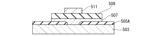
- FIG. 1 is a vertical cross-sectional view showing a quantum tunnel field effect transistor according to an embodiment of the present invention.
- FIG. 1 is a longitudinal cross-sectional view showing a quantum tunnel field effect transistor according to an embodiment of the present invention.
- FIG. 3 is a longitudinal cross-sectional view showing another embodiment of a quantum tunnel field effect transistor.
- FIG. 3 is a vertical cross-sectional view for explaining the manufacturing procedure of a quantum tunnel field effect transistor.
- FIG. 3 is a vertical cross-sectional view for explaining the manufacturing procedure of a quantum tunnel field effect transistor.
- FIG. 3 is a vertical cross-sectional view for explaining the manufacturing procedure of a quantum tunnel field effect transistor.
- FIG. 3 is a vertical cross-sectional view for explaining the manufacturing procedure of a quantum tunnel field effect transistor.
- FIG. 3 is a vertical cross-sectional view for explaining the manufacturing procedure of a quantum tunnel field effect transistor.
- 1 is a top view showing a display device using a thin film transistor according to an embodiment of the present invention.
- 2 is a diagram showing a circuit of a pixel section that can be applied to a pixel of a VA type liquid crystal display device.
- 1 is a diagram showing a circuit of a pixel portion of a display device using an organic EL element.
- 1 is a diagram showing a circuit of a pixel portion of a solid-state image sensor using a thin film transistor according to an embodiment of the present invention.
- 1 is an X-ray diffraction pattern of the oxide sintered body produced in Example 1.
- 2 is a mapping image of oxygen atoms in the oxide sintered body produced in Example 1.
- film or “thin film” and the term “layer” may be interchanged with each other in some cases.
- the "oxide sintered body” may be simply referred to as the "sintered body”.
- a “sputtering target” may be simply referred to as a "target.”
- electrically connected includes a case where a connection is made via "something that has some kind of electrical effect.”
- something that has some kind of electrical effect is not particularly limited as long as it enables transmission and reception of electrical signals between connected objects.
- something that has some kind of electrical action includes electrodes, wiring, switching elements (such as transistors), resistance elements, inductors, capacitors, and other elements with various functions.
- the functions of the source and drain of a transistor may be interchanged when transistors with different polarities are used or when the direction of current changes during circuit operation. Therefore, in this specification and the like, the terms source and drain can be used interchangeably.
- a numerical range expressed using “ ⁇ ” means a range that includes the numerical value written before “ ⁇ ” as the lower limit and the numerical value written after " ⁇ " as the upper limit. do.
- the present inventors invented the present invention based on the following findings. Cracks that occur during sputtering film formation at high power (high output) are caused by the surface of the sputtering target exposed to high-energy plasma becoming highly heated, and the temperature between the surface of the target and the back surface of the target being cooled. This is thought to be due to the generation of thermal stress due to the difference. Examples of parameters related to the occurrence of cracks include (1) flexural strength, (2) thermal conductivity, (3) coefficient of linear expansion, and (4) Young's modulus.
- the above (2) thermal conductivity, (3) coefficient of linear expansion, and (4) Young's modulus can be improved by changing the crystal structure and the ratio of the constituent crystals. You can change the value to some extent.
- (1) the bending strength can be improved by suppressing pores in the sintered body or reducing the average grain size of the crystal phase. Therefore, in order to improve the crack resistance (hereinafter, this resistance may be referred to as power resistance) when sputtering a film at high power (high output), it is effective to increase the bending strength. It is.
- the present inventors have determined that, in a sputtering target equipped with an oxide sintered body containing In element, Ga element, and O element, the crystal structure contained in the sintered body and the atomic composition ratio of Ga element are Through this study, we obtained the knowledge that sputtering film formation at high output is possible. The present inventors also discovered that in a sputtering target equipped with an oxide sintered body containing an In element, a Ga element, and an O element, the crystal structure contained in the sintered body, the atomic composition ratio of the Ga element, and By examining the average grain size of the crystal structure represented by In 2 O 3 , we have found that it becomes possible to form a film by sputtering at high output and to improve crack resistance.
- the sputtering target according to this embodiment includes a sintered body.
- the sintered body becomes a film raw material when forming a film by sputtering. That is, the sputtering target according to the present embodiment includes an oxide sintered body containing In element, Ga element, and O element.
- the sintered body includes a crystal structure represented by In2O3 , the atomic composition ratio of the Ga element in the oxide sintered body satisfies the following formula (1), and the oxide sintered body
- the bending strength is 140 MPa or more. 8 ⁇ Ga/(In+Ga) ⁇ 20 (1)
- In and Ga represent the number of atoms of indium element and gallium element in the sintered body, respectively.
- the sintered body included in the target according to the present embodiment includes a crystal structure represented by In 2 O 3 .
- the sintered body may include another crystal structure such as GaInO 3 in addition to the crystal structure represented by In 2 O 3 .
- the ratio of the crystal structure represented by In 2 O 3 in the sintered body according to the present embodiment is preferably substantially 80% or more in terms of area ratio. Therefore, the crystal structure represented by In 2 O 3 is preferably the main phase in the sintered body included in the target according to the present embodiment.
- the crystal structure represented by In 2 O 3 is a bixbite phase.
- the ratio of the crystal structure represented by In 2 O 3 in the sintered body is determined by measuring the X-ray diffraction (XRD) of the sintered body, and calculating the peak area of the strongest line of each crystal phase and the RIR value ( Reference Intensity Ratio).
- the crystal phase of the sintered body has a crystal structure represented by In 2 O 3 (i.e., a bixbite phase represented by In 2 O 3 ) and a crystal structure represented by GaInO 3 .
- the ratio of the crystal structure represented by In 2 O 3 is the ratio of the crystal structure represented by In 2 O 3 to the entire crystal structure of the crystal structure represented by In 2 O 3 and the crystal structure represented by GaInO 3 . This is the ratio of the crystal structure represented by O3 .
- the crystal phase of the sintered body when the crystal phase of the sintered body is composed of a crystal structure represented by In 2 O 3 , a crystal structure represented by GaInO 3 , and a crystal structure A described below, In 2
- the ratio of the crystal structure represented by O 3 is the ratio of the crystal structure represented by In 2 O 3 to the entire crystal structure of the crystal structure represented by In 2 O 3, the crystal structure represented by GaInO 3 , and the crystal structure A. is the proportion of crystal structure.
- the average grain size of the crystal structure represented by In 2 O 3 contained in the sintered body is preferably 3 ⁇ m or less. That is, it is preferable that the average grain size of the crystal structure represented by In 2 O 3 as the main phase is 3 ⁇ m or less. If the average grain size of the crystal structure represented by In 2 O 3 contained in the sintered body is 3 ⁇ m or less, the bending strength of the sintered body is improved, and as a result, the power resistance is further improved.
- the average grain size of the crystal structure represented by In 2 O 3 is more preferably 2.5 ⁇ m or less, and even more preferably 2 ⁇ m or less.
- the lower limit of the average grain size of the crystal structure represented by In 2 O 3 is not particularly limited, and may be, for example, 1 ⁇ m or more.
- the crystal structure represented by GaInO 3 is included, for example, in addition to the crystal structure represented by In 2 O 3 contained as the main phase, In It is also conceivable to reduce the average grain size of the crystal structure represented by GaInO 3 instead of the average grain size of the crystal structure represented by 2 O 3 .
- the average grain size of the crystal structure represented by GaInO 3 is made small, it is difficult to obtain excellent flexural strength if the average grain size of the crystal structure represented by In 2 O 3 , which is the main phase, is large. .
- the average grain size of the crystal structure represented by In 2 O 3 can be calculated as follows. First, the polished sintered body is observed using a SEM, and a secondary electron image and a backscattered electron image are observed at a magnification of 2000 times. When observing by SEM, the atomic ratio of each crystal particle is determined using energy dispersive X-ray spectroscopy (EDS). Further, the crystal phase is confirmed by measuring the sintered body by X-ray diffraction (XRD). Next, each crystal phase is identified by comparing it with the crystal structure identified by X-ray diffraction (XRD). The crystal grains are measured using the obtained SEM image, and the average value of the grain size is calculated.
- EDS energy dispersive X-ray spectroscopy
- the average grain size of the crystal structure represented by In 2 O 3 can be measured, for example, as follows. If the planar shape of the sintered body is a square, divide the surface of the sintered body into 16 equal areas, cut out 1 cm squares at 16 center points of each square, and perform mirror polishing. Use as a sample for measurement. The measurement surface of the cut out sintered body is further divided into 9 equal areas, and a secondary electron image and a backscattered electron image are observed at 2000x magnification at 9 center points of each square. During SEM observation, EDS measurement is performed and compared with the crystal structure identified by XRD to identify which crystal each crystal particle is.
- the particle size is measured from the obtained SEM image, and the average value of the particle size of the particles within the frame at nine locations is determined. This operation is performed on measurement samples cut out from 16 locations, and the average value of the particle diameters obtained from a total of 144 SEM images is defined as the average particle diameter.
- the grain size is measured based on JIS R 1670:2006, with the grain size of the crystal grains as equivalent circle diameter. Specifically, as a procedure for measuring the equivalent circle diameter, a circular ruler is applied to the grain to be measured in the microstructure photograph, and the diameter corresponding to the area of the grain to be measured is read. For particles with an aspect ratio of 2 or more, the average value of the longest diameter and the shortest diameter is taken as the particle size of the particle. More specifically, this can be confirmed by the method described in the Examples below.
- the crystal phase of the sintered body has a crystal structure represented by In2O3 , and also has an incident angle (2 ⁇ ) determined by X-ray (CuK ⁇ ray) diffraction measurement.
- the crystal structure A includes a crystal structure A in which diffraction peaks are observed at each of the positions (A) to (E) below.
- the sintered body may further include the above-mentioned crystal structure A as a crystal phase contained in the sintered body. preferable. (A) 28° or more, 29° or less (B) 45° or more, less than 46° (C) 46° or more, less than 47° (D) 47° or more, 48° or less (E) 50° or more, 51° or less
- the crystal phase of the sintered body according to this embodiment includes the crystal structure A, it is possible to change the values of the thermal conductivity, linear expansion coefficient, and Young's modulus of the sintered body, and as a result, Even if the film is formed with high power, cracks are more likely to be suppressed.
- the sintered body included in the target according to the present embodiment has a crystal structure in which the content of O element (oxygen element) is different in the elemental mapping image, and a region where the content of O element (oxygen element) is relatively small. It is preferable that the regions have a relatively high content of O element (oxygen element) and a region with a relatively low content of O element are continuous.
- a structure with a low content of O element that is, a structure with many oxygen defects, has a low resistance value.
- the continuous connection (continuous connection) of this crystal structure with a low O element content makes it possible to keep the resistance value of the entire sintered body low, and as a result, it can be formed with high power. Even with a film, the occurrence of cracks can be more easily suppressed. If the resistance value of the sintered body is high, it may cause abnormal discharge and cause cracks to occur when forming a film at high power (high output).
- the elemental mapping image of the sintered body can be evaluated using a scanning electron microscope (SEM)-energy dispersive X-ray spectroscopy (EDS).
- SEM scanning electron microscope
- EDS energy dispersive X-ray spectroscopy
- the surface roughness Ra (arithmetic mean roughness) of the sintered body is preferably 0.5 ⁇ m or less. Further, the sintered body included in the target according to the present embodiment has a surface roughness Ra (arithmetic mean roughness) of 0.5 ⁇ m or less, and has a ground surface without directionality. is preferred.
- the surface roughness Ra of the sintered body is more preferably less than 0.5 ⁇ m, and even more preferably 0.25 ⁇ m or less.
- the surface roughness Ra of the sintered body included in the target according to this embodiment is 0.5 ⁇ m or less, preferably, the surface roughness Ra of the sintered body included in the target according to this embodiment is 0.5 ⁇ m or less, and If the polishing surface has a non-directional polishing surface, abnormal discharge and generation of particles can be prevented. Further, in the sintered body included in the target according to the present embodiment, it is preferable that the surface roughness Rz (maximum height roughness) of the surface of the sintered body is less than 2.0 ⁇ m. When the surface roughness Rz is less than 2.0 ⁇ m, a sputtering target with improved crack resistance is likely to be obtained. Examples of methods for adjusting the surface roughness Ra and surface roughness Rz of the sintered body include the method described below in the sputtering target manufacturing process.
- the atomic composition ratio of the Ga element satisfies the following formula (1). 8 ⁇ Ga/(In+Ga) ⁇ 20 (1)
- the atomic composition ratio of Ga (Ga/(In+Ga)) expressed by the above formula (1) is 8 or more, Ar gas and O 2 commonly used
- Ar gas and O 2 commonly used
- the thin film immediately after forming from becoming a completely crystalline film and from forming a thin film containing microcrystals in the thin film immediately after forming, and to improve patterning during TFT fabrication.
- generation of residue is suppressed.
- a residue may be generated by etching using a weak acid such as oxalic acid when manufacturing a TFT. , it becomes difficult to obtain the desired TFT characteristics.
- Ga/(In+Ga) is more preferably 10 or more, and even more preferably 12 or more.
- the thin film after being formed may be subjected to high-temperature annealing treatment, laser annealing treatment, etc. Even without special annealing treatment, the thin film after being formed can be easily crystallized by heat treatment (annealing treatment) at about 300° C. to 450° C. Furthermore, the thin film can be made larger without using expensive equipment. If the thin film is insufficiently crystallized after the thin film is annealed, the TFT including the insufficiently crystallized thin film may not be able to secure high mobility and stability.
- Ga/(In+Ga) is more preferably 18 or less, and even more preferably 16 or less.
- the sintered body included in the target according to the present embodiment may substantially consist only of In (indium) element, Ga (gallium) element, and O (oxygen) element.
- substantially means that the sintered body according to the present embodiment does not contain other components within the range where the effects of the present invention resulting from the combination of the In element, Ga element, and O element are produced. It means that it is okay to stay.
- the sintered body included in the target according to the present embodiment the sintered body may contain an element that is an impurity.
- the total content of In element and Ga element is preferably 99 at% or more with respect to the total (100 at%) of the metal elements in the sintered body, and 99 It is more preferably .5 atom % or more, and even more preferably 99.9 atom % or more.
- the total content of In element and Ga element may be 100 atomic % with respect to the total of metal elements in the sintered body. Note that in this specification, atomic % may be expressed as at %.
- Impurities are elements that are not intentionally added and are mixed in raw materials, manufacturing processes, etc. That is, impurities are unavoidable impurities that are inevitably included.
- Examples of impurities include alkali metal elements (elements such as Li (lithium), Na (sodium), K (potassium), and Rb (rubidium)), alkaline earth metal elements (elements such as Mg (magnesium), Ca (calcium), ), Sr (strontium), Ba (barium), etc.), H element (hydrogen element), B element (boron element), C element (carbon element), N element (nitrogen element), F element (fluorine element) , Si element (silicon element), and at least one element selected from the group consisting of Cl element (chlorine element), Zr element (zirconium element), Al element (aluminum element), and Sn element (tin element).
- the sintered body may contain H element (hydrogen element).
- the atomic concentration of the H element in the sintered body is preferably 1 ⁇ 10 16 cm ⁇ 3 or more and less than 1 ⁇ 10 18 cm ⁇ 3 .
- the atomic concentration of H element in the sintered body is more preferably 3 ⁇ 10 16 cm ⁇ 3 or more, and even more preferably 5 ⁇ 10 16 cm ⁇ 3 or more. If the H element concentration in the sintered body is too low, the effect of the H element degassed from the adhesion prevention plate of the sputtering chamber during film formation will be large, and the degassed H element will be mixed unevenly into the formed film.
- the atomic concentration of H element in the sintered body is more preferably 5 ⁇ 10 17 cm ⁇ 3 or less, and even more preferably 3 ⁇ 10 17 cm ⁇ 3 or less. If the concentration of H element in the sintered body is too high, a large amount of H element will be mixed into the formed film, which will form a donor level or acceptor level, and as a result, the reliability of TFT will be greatly deteriorated. It may be easier to connect with what you do.
- the sintered body may contain C element (carbon element).
- the lower limit of the atomic concentration of C in the sintered body is not particularly limited, and the amount of impurities during target production may be 1 ⁇ 10 16 cm ⁇ 3 .
- the atomic concentration of C element is preferably 1 ⁇ 10 16 cm ⁇ 3 or more and less than 1 ⁇ 10 18 cm ⁇ 3 .
- the atomic concentration of the C element in the sintered body is more preferably 7 ⁇ 10 17 cm ⁇ 3 or less, and even more preferably 4 ⁇ 10 17 cm ⁇ 3 or less.
- the atomic concentration of the C element is too high, a large amount of the C element will be mixed into the formed film, which will form a donor level or an acceptor level, resulting in a significant deterioration of the reliability of the TFT. It may be easier to connect.
- the sintered body may contain an H element (hydrogen element) and a C element (carbon element).
- the atomic concentrations of the H element and the C element are both 1 ⁇ 10 16 cm ⁇ 3 or more and less than 1 ⁇ 10 18 cm ⁇ 3 . preferable.
- the unit [atoms/cm 3 ] for the atomic concentration of element H and element C is sometimes expressed as [cm ⁇ 3 ].
- the atomic concentration of H element and C element contained in the sintered body can be determined by secondary ion mass spectrometry (SIMS) measurement.
- SIMS secondary ion mass spectrometry
- a dynamic SIMS device can be used for SIMS measurement.
- the sintered body included in the target according to the present embodiment may contain one or more elements selected from the group consisting of positive trivalent, positive tetravalent, and positive pentavalent elements as long as the effect is not impaired. may contain an element (X element).
- the sputtering target according to the present embodiment includes one or more elements selected from the group consisting of In element, Ga element, O element, and positive trivalent, positive tetravalent, and positive pentavalent.
- the oxide sintered body may include an oxide sintered body containing the X element. Even in this case, in one embodiment, the oxide sintered body includes a crystal structure represented by In 2 O 3 , and the atomic composition ratio of the Ga element in the oxide sintered body is as described above. Formula (1) is satisfied, and the oxide sintered body has a bending strength of 140 MPa or more. Further, the sintered body included in the sputtering target in this embodiment may include a crystal structure represented by GaInO 3 or may include the crystal structure A described above. Furthermore, in the sintered body included in the sputtering target in this embodiment, the average grain size of the crystal structure represented by In 2 O 3 may be 3 ⁇ m or less.
- the additive element X element is, for example, Zn (zinc) element, Mg (magnesium) element, Ti (titanium) element, Fe (iron) element, Zr (zirconium) element, Nb (niobium) element, Hf (hafnium) element.
- the additive element X is at least one of Zn (zinc) element and Sn (tin) element.
- the sintered body included in the sputtering target in this embodiment may substantially consist only of In (indium) element, Ga (gallium) element, O (oxygen) element, and X element. "Substantially" has the same meaning as above.
- the total content of In element, Ga element, and X element is 99 atomic % or more with respect to the total (100 atomic %) of the metal elements in the sintered body.
- the content is preferably 99.5 atom % or more, more preferably 99.9 atom % or more.
- the total content of In element, Ga element, and X element may be 100 atomic % with respect to the total of metal elements in the sintered body.
- the amount of element X which is an additive element, is preferably 2 at% or less, more preferably 1 at% or less, and even more preferably 0.5 at% or less.
- amount of the additive element is 2 at % or less, when a TFT is manufactured using the target according to this embodiment, it is easy to obtain a TFT with high mobility and high stability.
- the amount of added elements increases, the obtained TFT may have problems such as a decrease in mobility and a decrease in stability.
- the amount of element X, which is an additive element is expressed by the following formula (2). 0.02 ⁇ (X/(In+Ga+X))...(2)
- In, Ga, and X represent the number of atoms of indium element, gallium element, and X element in the sintered body, respectively.
- the content (atomic ratio) of each metal element in the sintered body can be determined by measuring the abundance of each element by ICP (Inductive Coupled Plasma) measurement or XRF (X-ray Fluorescence) measurement.
- ICP Inductive Coupled Plasma
- XRF X-ray Fluorescence
- An inductively coupled plasma emission spectrometer can be used for ICP measurement.
- a thin film fluorescent X-ray analyzer can be used for the XRF measurement.
- the density measured by the Archimedes method of the sintered body is 6.3 g/cm 3 or more. It is more preferable that the density of the sintered body measured by the Archimedes method is 6.5 g/cm 3 or more.
- the relative density of the sintered body is preferably 97% or more, more preferably 99% or more.
- Relative density means a percentage of the value obtained by dividing the actual density of the oxide sintered body measured by the Archimedes method by the theoretical density of the oxide sintered body.
- the thickness of the sintered body is usually preferably 2 mm or more and 20 mm or less.
- the thickness of the sintered body is more preferably 3 mm or more, and even more preferably 4 mm or more.
- the thickness of the sintered body is more preferably 12 mm or less, even more preferably 9 mm or less, even more preferably 6 mm or less.
- the sintered body included in the target according to this embodiment has a bending strength of 140 MPa or more.
- the bending strength is preferably 150 MPa or more, more preferably 160 MPa or more.
- the bending strength of the sintered body suppresses the occurrence of cracks when a film is formed by sputtering at high power (high output).
- the bending strength of the sintered body is determined based on JIS R 1601:2008 as the average value of the three-point bending strength measurements of 30 test pieces.
- the sintered body included in the target according to this embodiment also exhibits excellent physical properties such as thermal conductivity, coefficient of linear expansion, and Young's modulus.
- the linear expansion coefficient of the sintered body can be measured in accordance with JIS R 1618:2002 at a measurement temperature of 30° C. to 500° C., a temperature increase rate of 10 K/min, and an air atmosphere.
- the Young's modulus of the sintered body can be measured in accordance with JIS R 1602:1995 using an ultrasonic flaw detector at room temperature in the atmosphere.
- the thermal conductivity of the sintered body is determined by measuring the specific heat capacity by the laser flash method (at room temperature, in vacuum) and by measuring the thermal diffusivity by the laser flash method (at room temperature, in the atmosphere) in accordance with JIS R 1611:2010. Then, the thermal conductivity can be calculated from the following formula (Equation 1).
- ⁇ (thermal conductivity) Cp (specific heat capacity) x ⁇ (density) x ⁇ (thermal diffusivity) ... (Math. 1)
- ⁇ is the density of the oxide sintered body.
- the sputtering target according to this embodiment includes an oxide sintered body and cooling and holding members such as a backing plate provided on the oxide sintered body as necessary.
- the material of the backing plate which is a member for holding and cooling the oxide sintered body, is preferably a material with excellent thermal conductivity such as copper.
- the sintered body provided in the sputtering target according to this embodiment has a bonding surface attached to the holding member, and a bonding surface attached to the holding member. It has a sputtering surface which is a surface opposite to the surface and is sputtered.
- the sputtering surface is a smooth surface (that is, a smooth surface with the above-mentioned surface roughness Ra of 0.5 ⁇ m or less), and the surface opposite to the sputtering surface can be used as the bonding surface. preferable.
- the shape of the sputtering target is not particularly limited.
- the sputtering target may be, for example, plate-shaped as shown by reference numeral 1 in FIG. 1A, or cylindrical as shown by reference numeral 1A in FIG. 1B.
- the planar shape may be rectangular as shown by reference numeral 1 in FIG. 1A, or circular as shown by reference numeral 1B in FIG. 1C.
- the oxide sintered body may be integrally molded, or it may be of a multi-segmented type in which a plurality of divided oxide sintered bodies (symbol 1C) are each fixed to the backing plate 3, as shown in FIG. 1D.
- the method for manufacturing a sputtering target according to the present embodiment preferably includes, for example, the following steps.
- a step of preparing a raw material powder having a particle size of 0.5 ⁇ m or less (hereinafter sometimes referred to as a raw material powder preparation step).
- a step of mixing the raw material powders to obtain a raw material mixture, and then granulating the raw material mixture to obtain a raw material granule (hereinafter sometimes referred to as a granulation step).
- a step of molding the raw material granules to obtain a molded body hereinafter sometimes referred to as a molding step).
- a process of sintering the molded body to obtain a sintered body (hereinafter sometimes referred to as a sintering process).
- a preferable method for manufacturing the target according to the present embodiment further includes a step of heat-treating the sintered body (annealing step), a step of at least grinding the sintered body (hereinafter sometimes referred to as a grinding step), At least one selected from the group consisting of a process of cleaning the compact (hereinafter sometimes referred to as a cleaning process), and a process of bonding the sintered body to a backing plate (hereinafter sometimes referred to as a bonding process). It may have one step.
- raw material powder preparation process raw material powder to be used as a raw material for the sintered body included in the sputtering target according to the present embodiment is prepared.
- the raw material powders prepared in the raw material powder preparation step are indium oxide with an average particle size of 0.5 ⁇ m or less, and gallium oxide with an average particle size of 0.5 ⁇ m or less.
- the raw material powder is, if necessary, a raw material powder of a compound containing one or more elements selected from the group consisting of positive trivalence, positive tetravalence, and positive pentavalence, and having an average particle size of 0.5 ⁇ m or less. You may also prepare.
- the raw material powder may be prepared by obtaining a raw material powder having an average particle size of 0.5 ⁇ m or less, or may be prepared by obtaining a raw material powder having an average particle size of more than 0.5 ⁇ m, and the average particle size of the obtained raw material powder. may be adjusted to 0.5 ⁇ m or less.
- the average particle size of the raw material powder prepared in the raw material powder preparation step is preferably 0.1 ⁇ m or more and 0.5 ⁇ m or less.
- the average particle size of the raw material powder is 0.1 ⁇ m or more, aggregation of the raw material powders is easily suppressed, and the raw material powders can be mixed almost uniformly.
- the average particle size of the raw material powder is 0.5 ⁇ m or less, the average particle size of the crystal structure represented by In 2 O 3 contained in the sintered body after sintering can be easily controlled to 3 ⁇ m or less.
- the average particle size of the raw material powder can be calculated by at least one of the following methods: particle size evaluation using a particle size distribution analyzer and specific surface area determined by the BET method. Further, the average particle size of the raw material powder can also be confirmed using a SEM device.
- the average particle size of the obtained raw material powder exceeds 0.5 ⁇ m, it is preferable to pre-pulverize the raw material powder to adjust the average particle size of the raw material powder to 0.5 ⁇ m or less.
- Preliminary pulverization can be performed using a bead mill, a ball mill, a jet mill, or the like.
- the material of the pot used in preliminary crushing is not particularly limited, and examples thereof include agate, alumina, and the like.
- the material of the grinding media (balls) used in the preliminary grinding is not particularly limited, and examples include materials such as alumina and zirconia.
- the grinding time in preliminary grinding is preferably 30 minutes or more and 6 hours or less.
- the grinding time in the preliminary grinding is 30 minutes or more, a sufficient grinding effect can be obtained and it becomes easier to adjust the average particle size to a predetermined average particle size. If the crushing time in preliminary crushing is 6 hours or less, the material of the pot and the material of the ball will be scraped and it will be difficult for foreign matter to get mixed in (contamination will be difficult to occur). When manufactured, it is easy to obtain a TFT with high mobility and high stability.
- a binder, a dispersant, an antifoaming agent, and the like may be appropriately added to the pulverization, if necessary.
- the raw material powders of indium oxide and gallium oxide prepared in the raw material powder preparation step have high purity.
- the purity of each raw material powder is preferably 99% by mass or more, more preferably 99.9% by mass or more, and even more preferably 99.99% by mass or more.
- the raw material powder when using a raw material powder of a compound containing one or more elements selected from the group consisting of positive trivalent, positive tetravalent, and positive pentavalent, the raw material powder also includes raw material powder of indium oxide and gallium oxide. Similarly, high purity is preferred.
- the purity of the raw material powder of a compound containing one or more elements selected from the group consisting of positive trivalence, positive tetravalence, and positive pentavalence is preferably 99% by mass or more, and 99.9% by mass. % or more, and even more preferably 99.99% by mass or more.
- a high-purity raw material powder is used, a sintered body with a dense structure can be obtained, and the volume resistivity of a sputtering target including the sintered body is reduced.
- a TFT is manufactured using a sputtering target including the sintered body, formation of defect levels due to impurities can be suppressed, and a TFT with high mobility and high stability can be obtained.
- the raw material powders prepared in the raw material powder preparation step described above are mixed to form a mixed raw material powder, and if necessary, a dispersant, a thickener, etc. are added to form a raw material mixture.
- the mixed raw material powder may be used as a raw material mixture as it is.
- the raw material mixture is granulated to obtain raw material granules.
- the raw material granules may be referred to as raw material granulated powder.
- a dispersant to break up the agglomeration and a thickener to adjust the viscosity to be suitable for granulation in a spray dryer are added to the raw material powder prepared in the raw material powder preparation process, and then the raw material powder is added to the raw material powder prepared in the raw material powder preparation process.
- a raw material mixture may be obtained by mixing using a ball mill, bead mill, jet mill, or the like. Among these, the device used for water mixing is preferably a bead mill.
- Using a bead mill allows the raw material powder to be mixed uniformly, which allows sufficient sintering at the sintering temperatures described below, making it easier to obtain a sputtering target that allows sputtering film formation at high power (high output).
- the dispersant include ammonia neutralized acrylic acid methacrylic acid copolymer
- examples of the thickener include polyvinyl alcohol.
- the mixing time of the raw material powders is not particularly limited as long as the raw material powders are sufficiently mixed. It is preferable that the mixing time of the raw material powder is, for example, 2 hours or more and 48 hours or less. When the mixing time is 2 hours or more, the raw material powder is likely to be sufficiently mixed. When the mixing time is 48 hours or less, the occurrence of re-agglomeration of the raw material powder is likely to be suppressed. Further, when the mixing time is 48 hours or less, contamination with foreign substances from the pot material, the ball material, etc. is suppressed.
- the granulation process for granulating the raw material mixture can be performed using a spray dryer or the like.
- the shape of the raw material granules obtained in the granulation step is not particularly limited, and is preferably perfectly spherical in order to uniformly fill the mold in the molding step described below.
- the granulation conditions are appropriately selected by adjusting the concentration of the raw material mixture after mixing the raw material powders introduced into the spray dryer, the rotation speed of the spray dryer, the hot air temperature used for drying, etc.
- the raw material mixture obtained above may be used as it is to prepare the raw material granules.
- the calcined raw material mixture may be prepared into a pulverized raw material mixture again by the method described in the pre-pulverization of the raw material powder and then used.
- the particle size of the raw material granules formed by the granulation process is not particularly limited, and is preferably controlled within a range of, for example, 25 ⁇ m or more and 150 ⁇ m or less.
- the particle size of the raw material granules is 25 ⁇ m or more, the slipperiness of the raw material granules on the surface of the mold used in the molding process described later improves, and the raw material granules can be sufficiently filled into the mold. .
- the particle size of the raw material granules is 150 ⁇ m or less, it is possible to prevent the particle size from being too large and reducing the filling rate in the mold.
- the particle size of the raw material granules is more preferably 25 ⁇ m or more and 75 ⁇ m or less.
- the method for obtaining raw material granules having a particle size within a desired range is not particularly limited.
- a method may be used in which raw material granules that have been subjected to granulation treatment are sieved to select raw material granules that fall within a desired particle size range.
- the sieve used in this method is preferably a sieve having openings large enough to allow raw material granules of a desired particle size to pass through.
- the sieves used in this method include a first sieve for sorting the raw material granules based on the lower limit of the particle size range, and a second sieve for sorting the raw material granules based on the upper limit of the particle size range.
- a sieve is used.
- the size is such that raw material granules of less than 25 ⁇ m can pass through, and raw material granules of 25 ⁇ m or more do not pass.
- a sieve (first sieve) having openings raw material granules having a particle size of 25 ⁇ m or more are selected.
- the raw material granules after sorting are passed through a sieve (second sieve) having an opening size that allows raw material granules of 150 ⁇ m or less to pass through, but does not allow raw material granules of more than 150 ⁇ m to pass through. Then, raw material granules with a size of 25 ⁇ m or more and 150 ⁇ m or less are selected.
- the second sieve may be used first, and then the first sieve may be used.
- the method for controlling the particle size range of the raw material granules is not limited to the method using a sieve as described above, and any method may be used as long as the raw material granules to be subjected to the molding process can be controlled within a desired range.
- the raw material granules are molded by a method such as die press molding, cast molding, or injection molding to obtain a molded body.
- a method such as die press molding, cast molding, or injection molding to obtain a molded body.
- CIP cold isostatic pressing
- sintering process In the sintering process, a sintered body is obtained by sintering the molded body obtained in the molding process. In the sintering process, a commonly used sintering method such as pressureless sintering, hot press sintering, or hot isostatic pressing (HIP) sintering can be used. The obtained sintered body becomes a sputtering target material.
- a commonly used sintering method such as pressureless sintering, hot press sintering, or hot isostatic pressing (HIP) sintering can be used.
- the obtained sintered body becomes a sputtering target material.
- the sintering temperature is preferably 1300°C or higher and 1400°C or lower.
- the sintering temperature is 1300° C. or higher, the sintering of the molded body sufficiently progresses, thereby suppressing the generation of a large number of pores in the sintered body, and easily improving the bending strength.
- the sintering temperature is 1400° C. or less, the average grain size of the crystal structure represented by In 2 O 3 contained in the sintered body can be easily controlled to a range of 3 ⁇ m or less, and the bending strength can be easily improved.
- the sintering time is preferably 12 hours or more and 48 hours or less.
- the sintering time is 12 hours or more, the sintering of the molded body sufficiently progresses, thereby suppressing the generation of a large number of pores in the sintered body, and easily improving the bending strength.
- the sintering time is 48 hours or less, the average grain size of the crystal structure represented by In 2 O 3 contained in the sintered body can be easily controlled to a range of 3 ⁇ m or less, and the bending strength can be easily improved.
- the rate of temperature increase from room temperature to the sintering temperature is not particularly limited, and is preferably 0.1° C./min or more and 3° C./min or less.
- the temperature may be maintained at 700° C. or more and 800° C. or less for 1 hour or more and 10 hours or less, and after being maintained at a predetermined temperature for a predetermined time, the temperature may be raised to the sintering temperature.
- Examples of the atmosphere during sintering include an atmosphere of air or oxygen gas, an atmosphere containing air or oxygen gas and a reducing gas, or an atmosphere containing air or oxygen gas and an inert gas.
- Examples of the reducing gas include hydrogen gas, methane gas, and carbon monoxide gas.
- Examples of the inert gas include argon gas and nitrogen gas.
- the obtained sintered body is annealed.
- the annealing step is a step provided as necessary.
- the sintered body is usually treated at a holding temperature of 700° C. or higher and 1100° C. or lower, and for a holding time of 1 hour or more and 5 hours or less.
- the sintered body may be once cooled and then the temperature may be raised again for annealing, or the sintered body may be annealed when the temperature is lowered from the sintering temperature.
- Examples of the atmosphere during annealing include an atmosphere of air or oxygen gas, an atmosphere containing air or oxygen gas and a reducing gas, or an atmosphere containing air or oxygen gas and an inert gas.
- Examples of the reducing gas include hydrogen gas, methane gas, and carbon monoxide gas.
- Examples of the inert gas include argon gas and nitrogen gas.
- the obtained sintered body is cut into an appropriate shape, and the surface of the oxide sintered body is polished. Specifically, the sintered body is cut into a shape suitable for attachment to a sputtering device, and the surface of the oxide sintered body is polished.
- the abrasive grain size of the grindstone used in the grinding process is preferably 100 ⁇ m or less. If the abrasive grain size of the grindstone is 100 ⁇ m or less, cracking of the sintered body can be prevented.
- the grindstone used in the grinding process is preferably a diamond grindstone.
- the grinding depth in the grinding step is preferably 0.3 mm or more, more preferably 0.5 mm or more, and even more preferably 2 mm or more. By grinding the surface of the sintered body by 0.3 mm or more, the portion where the crystal structure fluctuates near the surface can be removed.
- the surface of the sintered body that has undergone the grinding process preferably has a surface roughness Ra (arithmetic mean roughness) of 5 ⁇ m or less.
- the surface of the sintered body that has undergone the grinding process preferably has a surface roughness Rz (maximum height roughness) of less than 2.0 ⁇ m. Further, it is preferable that the surface of the sintered body subjected to the grinding process has a surface roughness Ra (arithmetic mean roughness) of 5 ⁇ m or less and has a ground surface without directionality.
- the sputtered surface of the sintered body may be further mirror-finished.
- known polishing techniques such as mechanical polishing, chemical polishing, and mechanochemical polishing (combination of mechanical polishing and chemical polishing) can be used.
- the polishing method is not limited to these methods.
- the cleaning process In the cleaning process, the sintered body ground in the grinding process is cleaned.
- the cleaning treatment include air blowing and running water washing. When removing foreign matter by air blowing, it is possible to remove the foreign matter more effectively by using a dust collector to draw air from the opposite side of the air blow nozzle.
- ultrasonic cleaning or the like in addition to the cleaning treatment by air blowing or running water cleaning, ultrasonic cleaning or the like may be further performed.
- An effective method for ultrasonic cleaning is to perform multiple oscillations at a frequency of 25 kHz or more and 300 kHz or less. For example, it is preferable to perform ultrasonic cleaning by multiplexing 12 different frequencies at 25 kHz intervals between 25 kHz and 300 kHz.
- the bonding process is a process of bonding the sintered body after the processing process to the backing plate with a low melting point metal (for example, metal indium, metal gallium, etc.).
- a low melting point metal for example, metal indium, metal gallium, etc.
- the bonding rate is preferably 90% or more, more preferably 95% or more, and even more preferably 98% or more.
- the bonding ratio here indicates the area ratio of the surface where the target material and the target support material are bonded via the bonding layer to the area of the surface where the target material and the target support material overlap.
- the bonding rate can be confirmed by, for example, X-ray computed tomography (CT) or ultrasonic flaw detection.
- the sputtering target according to this embodiment since a target having the same atomic composition as the sintered body according to the present embodiment is used, the TFT obtained by sputtering has high mobility and high stability. is obtained.
- the crystalline oxide thin film according to this embodiment is a crystalline oxide thin film using the sputtering target according to this embodiment.
- the crystalline oxide thin film according to this embodiment is obtained by forming a film using the sputtering target according to this embodiment.
- the crystalline oxide thin film according to the present embodiment is produced by, for example, a step of forming an oxide thin film by sputtering using the sputtering target according to the present embodiment (hereinafter sometimes referred to as an oxide thin film deposition step). It is preferable that the oxide film be obtained by a manufacturing method including a step of subjecting an oxide thin film to a heat treatment (hereinafter sometimes referred to as a heat treatment step).
- a heat treatment step a manufacturing method including a step of subjecting an oxide thin film to a heat treatment
- the crystalline oxide thin film according to this embodiment is a crystalline oxide thin film.
- the crystalline oxide thin film according to this embodiment is an amorphous oxide thin film after sputtering film formation and before heat treatment (annealing treatment), and crystallinity is improved by annealing treatment after sputtering film formation. As a result, a crystalline oxide thin film is obtained. Since the crystalline oxide thin film according to this embodiment is a crystalline oxide thin film, a thin film transistor (TFT) including the crystalline oxide thin film according to this embodiment has high mobility and high stability. .
- TFT thin film transistor
- Whether the oxide thin film is amorphous or crystalline can be confirmed by X-ray diffraction (XRD) measurement of each oxide thin film.
- XRD X-ray diffraction
- a gas that does not substantially contain impurity gases is used.
- one or more gases selected from the group consisting of argon, hydrogen, and oxygen, which do not substantially contain impurity gases are used as the sputtering gas.
- the sputtering gas is preferably a mixed gas of argon and oxygen that does not substantially contain impurity gases.
- Sputtering gas "substantially does not contain any impurity gases” means that it does not contain argon, hydrogen, gases that cannot be eliminated (unavoidable impurity gases) such as adsorbed water introduced by gas insertion, chamber leaks, and adsorbed gases. This means that impurity gases other than oxygen are not actively introduced.
- the sputtering gas for example, a commercially available mixed gas of high purity argon and high purity oxygen can be used. Impurities are preferably excluded from the sputter gas if possible.
- the proportion of impurity gas in the sputtering gas is preferably 0.1% by volume or less, more preferably 0.05% by volume or less. If the proportion of impurity gas is 0.1% by volume or less, crystallization of the oxide thin film will proceed without any problem.
- the purity of high-purity argon and high-purity oxygen is preferably 99% by volume or more, more preferably 99.9% by volume or more, and even more preferably 99.99% by volume or more.
- the partial pressure of oxygen in the mixed gas of argon and oxygen which is the sputtering gas, is preferably in the range of 0% to 50% by volume, more preferably in the range of 5% to 30% by volume. If the oxygen partial pressure is within the above range, it will easily crystallize and become a semiconductor upon heating. By changing the oxygen partial pressure, the degree of oxidation of the obtained thin film, that is, the degree of crystallization, can be adjusted.
- the oxygen partial pressure may be appropriately selected as necessary.
- the heat treatment temperature for crystallizing the amorphous thin film after deposition is preferably in the range of 300°C to 450°C, more preferably 300°C to 350°C. If the heat treatment temperature is 300° C. or higher, the oxide thin film can be easily crystallized. When the heat treatment temperature is 450° C. or lower, abnormal growth of crystals and enlargement of crystal grains can be suppressed.
- the heat treatment time for crystallizing the amorphous thin film after film formation is preferably 0.1 hours or more and 5 hours or less, and preferably 0.3 hours or more and 3 hours or less. is more preferable, and even more preferably 0.5 hours or more and 2 hours or less. If the heat treatment time is 0.1 hour or more, crystallization will not occur and the oxide thin film will easily crystallize. If the heat treatment time is 5 hours or less, it is economical.
- the temperature increase rate is preferably 2° C./min or more and 40° C./min or less, more preferably 3° C./min or more and 20° C./min or less. If the temperature increase rate in the heat treatment step is 2° C./min or more, the production efficiency of the oxide thin film will be improved compared to the case where it is less than 1° C./min. If the temperature increase rate in the heat treatment step is 40° C./min or less, metal elements can be uniformly diffused during crystallization, and crystals in which metal is not segregated at grain boundaries can be formed.
- the crystalline oxide thin film according to this embodiment can also be applied to various integrated circuits such as logic circuits, memory circuits, and differential amplifier circuits, and can be applied to electronic devices and the like. Further, the crystalline oxide thin film according to this embodiment can be used in some layers of solar cells, liquid crystal elements, organic electroluminescent elements, inorganic electroluminescent elements, micro organic EL displays, micro LED (Light Emitting Diode) displays, and It can be applied as a part of a layer of a display device such as a mini LED display.
- the crystalline oxide thin film according to this embodiment can be used for solid-state imaging devices, X-ray sensors, power semiconductor devices, touch panels, LSIs (Large Scale Integrated circuits), resistance change memories, DRAMs (Dynamic Random Access Memory), and dielectric It can be applied as part of layers of memory, BEOL (Back End of Line), and microprocessors.
- the crystalline oxide thin film according to this embodiment can be used in semiconductor layers of field effect transistors, electrostatic induction transistors, quantum tunnel field effect transistors, Schottky barrier transistors, Schottky diodes, PN diodes, and resistance elements, and , they can also be adapted as some layers.
- Examples of the thin film transistor according to this embodiment include a thin film transistor including a crystalline oxide thin film according to this embodiment.
- the crystalline oxide thin film according to this embodiment is preferably an oxide semiconductor thin film.
- the crystalline oxide thin film according to this embodiment is preferable to use as a channel layer of a thin film transistor.
- the thin film transistor according to this embodiment has the crystalline oxide thin film according to this embodiment as a channel layer
- other element configurations in the thin film transistor are not particularly limited, and known element configurations can be adopted.
- the thin film transistor according to this embodiment can be suitably used in electronic devices. Specifically, the thin film transistor according to this embodiment can be suitably used in display devices such as liquid crystal displays and organic EL displays.
- the thickness of the channel layer in the thin film transistor according to this embodiment is usually 10 nm or more and 300 nm or less, preferably 20 nm or more and 250 nm or less.
- the channel layer in the thin film transistor according to this embodiment is normally used in an N-type region, but it can be used in a PN junction in combination with various P-type semiconductors such as a P-type Si-based semiconductor, a P-type oxide semiconductor, and a P-type organic semiconductor. It can be used for various semiconductor devices such as type transistors.
- the thin film transistor according to this embodiment can also be applied to various integrated circuits such as field effect transistors, logic circuits, memory circuits, and differential amplifier circuits. Furthermore, in addition to field effect transistors, the present invention can also be applied to electrostatic induction transistors, Schottky barrier transistors, Schottky diodes, and resistive elements. That is, the thin film transistor according to this embodiment can be applied to the applications exemplified in "Applications of Thin Film Transistors" described later.
- the structure of the thin film transistor according to this embodiment can be selected from known structures such as bottom gate, bottom contact, top gate, and top contact without any limitation.
- the thin film transistor according to this embodiment can be suitably used in a display device.
- the thin film transistor 100 includes a silicon wafer 20, a gate insulating film 30, an oxide thin film 40, a source electrode 50, a drain electrode 60, and interlayer insulating films 70 and 70A.
- the silicon wafer 20 is a gate electrode.
- the gate insulating film 30 is an insulating film that blocks conduction between the gate electrode and the oxide thin film 40, and is provided on the silicon wafer 20.
- the oxide thin film 40 is a channel layer and is provided on the gate insulating film 30.
- the crystalline oxide thin film according to this embodiment is used as the oxide thin film 40.
- the source electrode 50 and the drain electrode 60 are conductive terminals for allowing source current and drain current to flow through the oxide thin film 40, and are each provided so as to be in contact with both ends of the oxide thin film 40.
- the interlayer insulating film 70 is an insulating film that blocks electrical conduction between the source electrode 50 and drain electrode 60 and the oxide thin film 40 except for the contact portions.
- the interlayer insulating film 70A is an insulating film that blocks electrical conduction between the source electrode 50 and drain electrode 60 and the oxide thin film 40 except for the contact portions.
- the interlayer insulating film 70A is also an insulating film that blocks electrical conduction between the source electrode 50 and the drain electrode 60.
- the interlayer insulating film 70A is also a channel layer protective layer.
- the structure of the thin film transistor 100A is similar to that of the thin film transistor 100, except that a source electrode 50 and a drain electrode 60 are provided in contact with both the gate insulating film 30 and the oxide thin film 40. are different. Another difference is that an interlayer insulating film 70B is integrally provided so as to cover the gate insulating film 30, the oxide thin film 40, the source electrode 50, and the drain electrode 60.
- the materials for forming the drain electrode 60, the source electrode 50, and the gate electrode can be arbitrarily selected.
- a silicon wafer is used as the substrate, and the silicon wafer also acts as an electrode, but the electrode material is not limited to silicon.
- transparent electrodes such as indium tin oxide (ITO), indium zinc oxide (IZO), ZnO, and SnO2 , metal electrodes such as Al, Ag, Cu, Cr, Ni, Mo, Au, Ti, and Ta, Alternatively, metal electrodes or laminated electrodes made of alloys containing these can be used.
- the gate electrode may be formed on a substrate such as glass.
- interlayer insulating films 70, 70A, and 70B there is no particular restriction on the material for forming the interlayer insulating films 70, 70A, and 70B, and any commonly used material can be selected arbitrarily.
- materials for forming the interlayer insulating films 70, 70A, and 70B for example, compounds represented by MO x , MN x , and MN and y is a real number exceeding 0. The same applies to x and y in the compounds exemplified below.) Specifically, compounds such as SiO 2 , SiO x , SiN x , and SiN x O y can be used as the material.
- the materials include, for example, Al 2 O 3 , Ta 2 O 5 , TiO 2 , MgO, ZrO 2 , CeO 2 , K 2 O, Li 2 O, Na 2 O, Rb 2 O, Sc 2 O 3 , Compounds such as Y2O3 , HfO2 , CaHfO3, PbTiO3 , BaTa2O6 , SrTiO3 , Sm2O3 , and AlN can also be used.
- the valences of the anions (oxygen anions and nitrogen anions) in these oxide compounds and nitride compounds are not particularly limited, and may be real numbers greater than zero.
- the thin film transistor according to this embodiment is a back channel etch type (bottom gate type)
- a protective film on the drain electrode, source electrode, and channel layer.
- durability can be easily improved even when the TFT is driven for a long time.
- a gate insulating film is formed on a channel layer.
- the protective film or insulating film can be formed, for example, by CVD, but this may involve a process using high temperatures. Further, the protective film or the insulating film often contains impurity gas immediately after film formation, and therefore it is preferable to perform heat treatment (annealing treatment). By removing impurity gases through heat treatment, a stable protective film or insulating film can be obtained, making it easier to form a highly durable TFT element.
- the crystalline oxide thin film according to this embodiment it becomes less susceptible to the effects of temperature in the CVD process and subsequent heat treatment, so even when a protective film or insulating film is formed, the TFT characteristics stability can be improved.
- On/Off characteristics are a factor that determines the display performance of a display.
- the On/Off ratio is preferably 6 digits or more.
- the On current is important because of current drive, but the On/Off ratio is preferably 6 digits or more.
- the thin film transistor according to this embodiment preferably has an On/Off ratio of 1 ⁇ 10 6 or more.
- the mobility of the TFT according to this embodiment is preferably 5 cm 2 /Vs or more, and preferably 10 cm 2 /Vs or more.
- the saturation mobility is determined from the transfer characteristics when a drain voltage of 20V is applied. Specifically, it can be calculated by creating a graph of the transfer characteristic Id-Vg, calculating the transconductance (Gm) of each Vg, and finding the saturation mobility using the saturation region formula.
- Id is the current between the source and drain electrodes
- Vg is the gate voltage when voltage Vd is applied between the source and drain electrodes.
- the threshold voltage (Vth) is preferably -3.0V or more and 3.0V or less, more preferably -2.0V or more and 2.0V or less, and even more preferably -1.0V or more and 1.0V or less.
- the threshold voltage (Vth) is ⁇ 3.0 V or higher, a thin film transistor with high mobility can be obtained.
- the threshold voltage (Vth) is 3.0 V or less, a thin film transistor with a small off-state current and a large on-off ratio can be obtained.
- the On/Off ratio is preferably 10 6 or more and 10 12 or less, more preferably 10 7 or more and 10 11 or less, and even more preferably 10 8 or more and 10 10 or less.
- the On/Off ratio is 10 6 or more, a liquid crystal display can be driven.
- the On/Off ratio is 10 12 or less, an organic EL with high contrast can be driven.
- the On/Off ratio is 10 12 or less
- the off current can be reduced to 10 -11 A or less
- the image retention time can be extended, Sensitivity can be improved.
- the crystalline oxide thin film according to this embodiment can also be used in a quantum tunnel field effect transistor (FET).
- FET quantum tunnel field effect transistor
- the quantum tunnel field effect transistor may be referred to as a quantum tunnel field effect transistor.
- FIG. 4 shows a schematic diagram (vertical cross-sectional view) of a quantum tunnel field effect transistor (FET) according to one embodiment.
- the quantum tunnel field effect transistor 501 includes a p-type semiconductor layer 503, an n-type semiconductor layer 507, a gate insulating film 509, a gate electrode 511, a source electrode 513, and a drain electrode 515.
- the p-type semiconductor layer 503, the n-type semiconductor layer 507, the gate insulating film 509, and the gate electrode 511 are stacked in this order.
- Source electrode 513 is provided on p-type semiconductor layer 503.
- Drain electrode 515 is provided on n-type semiconductor layer 507.
- the p-type semiconductor layer 503 is a p-type group IV semiconductor layer, and here is a p-type silicon layer.
- the n-type semiconductor layer 507 here is the n-type oxide thin film according to the above embodiment.
- the source electrode 513 and the drain electrode 515 are conductive films.
- an insulating layer may be formed on the p-type semiconductor layer 503.
- the p-type semiconductor layer 503 and the n-type semiconductor layer 507 are connected through a contact hole, which is a region formed by partially opening an insulating layer.
- the quantum tunnel field effect transistor 501 may include an interlayer insulating film covering its upper surface.
- the quantum tunnel field effect transistor 501 is a quantum tunnel field effect transistor that performs current switching in which the current tunneling through the energy barrier formed by the p-type semiconductor layer 503 and the n-type semiconductor layer 507 is controlled by the voltage of the gate electrode 511. (FET).
- FET field effect transistor
- FIG. 5 shows a schematic diagram (vertical cross-sectional view) of a quantum tunnel field effect transistor 501A according to another embodiment.
- the configuration of quantum tunnel field effect transistor 501A is similar to quantum tunnel field effect transistor 501, except that a silicon oxide layer 505 is formed between p-type semiconductor layer 503 and n-type semiconductor layer 507.
- the presence of the silicon oxide layer allows the off-state current to be reduced.
- the thickness of the silicon oxide layer 505 is preferably 10 nm or less. By setting the thickness of the silicon oxide layer 505 to 10 nm or less, it is possible to prevent tunneling current from flowing, difficulty in forming an energy barrier, and changes in barrier height, thereby reducing tunneling current. , prevent changes.
- the thickness of the silicon oxide layer 505 is preferably 8 nm or less, more preferably 5 nm or less, still more preferably 3 nm or less, and even more preferably 1 nm or less.
- the n-type semiconductor layer 507 is an n-type oxide semiconductor.
- the oxide thin film constituting the n-type semiconductor layer 507 may be amorphous. Since the oxide thin film constituting the n-type semiconductor layer 507 is amorphous, it can be etched with organic acids such as oxalic acid, and the difference in etching speed with other layers becomes large, making it difficult to etch metal layers such as wiring. Etching can be performed well without any adverse effects.
- the oxide thin film constituting the n-type semiconductor layer 507 may be crystalline. Since the oxide thin film constituting the n-type semiconductor layer 507 is crystalline, the band gap becomes larger than in the case of an amorphous film, and the off-state current can be reduced. Since the work function can also be increased, it becomes easier to control the current tunneling through the energy barrier formed by the p-type group IV semiconductor material and the n-type semiconductor layer 507.
- the method for manufacturing the quantum tunnel field effect transistor 501 is not particularly limited, but the following method can be exemplified.
- an insulating film 505A is formed on the p-type semiconductor layer 503, and a contact hole 505B is formed by opening a part of the insulating film 505A by etching or the like.
- an n-type semiconductor layer 507 is formed on the p-type semiconductor layer 503 and the insulating film 505A. At this time, the p-type semiconductor layer 503 and the n-type semiconductor layer 507 are connected via the contact hole 505B.
- a gate insulating film 509 and a gate electrode 511 are formed in this order on the n-type semiconductor layer 507.
- an interlayer insulating film 519 is provided to cover the insulating film 505A, the n-type semiconductor layer 507, the gate insulating film 509, and the gate electrode 511.
- a contact hole 519A is formed by opening a part of the insulating film 505A on the p-type semiconductor layer 503 and the interlayer insulating film 519, and a source electrode 513 is provided in the contact hole 519A.
- a contact hole 519B is formed by opening part of the gate insulating film 509 and interlayer insulating film 519 on the n-type semiconductor layer 507, and a drain electrode 515 is formed in the contact hole 519B.
- the quantum tunnel field effect transistor 501 can be manufactured by the above procedure.
- the quantum tunnel field effect transistor 501A can be manufactured.
- the thin film transistor according to this embodiment is preferably a channel doped thin film transistor.
- a channel-doped thin film transistor is a transistor in which carriers in the channel are properly controlled by n-type doping, rather than by oxygen vacancies, which tend to fluctuate in response to external stimuli such as atmosphere and temperature, resulting in high mobility and high reliability. Compatible effects can be obtained.
- the thin film transistor according to this embodiment can be suitably used in solar cells, display elements (liquid crystal elements, organic electroluminescent elements, inorganic electroluminescent elements, etc.), and power semiconductor elements.
- the thin film transistor according to the present embodiment can be used in display devices (liquid crystal displays, organic EL (electro luminescence) displays, micro organic EL displays, micro LED (light emitting diode) displays, mini LED displays, etc.), solid-state image sensors, touch panels, etc.
- the present invention can be suitably used as a transistor in a device using an active matrix method.
- the thin film transistor according to this embodiment can also be applied to various integrated circuits such as field effect transistors, logic circuits, memory circuits, and differential amplifier circuits, and can be applied to electronic devices and the like.
- the electronic device according to this embodiment preferably includes a thin film transistor.
- the thin film transistor according to this embodiment can be applied not only to field effect transistors but also to static induction transistors and Schottky barrier transistors.
- the thin film transistor according to this embodiment can also be applied as a transistor for sensors such as image sensors, X-ray sensors, and biological sensors.
- FIG. 7A is a top view of the display device according to this embodiment.
- FIG. 7B is a circuit diagram for explaining a circuit of a pixel section when a liquid crystal element is applied to the pixel section of the display device according to this embodiment.
- FIG. 7C is a circuit diagram for explaining a circuit of a pixel section when an organic EL element is applied to the pixel section of the display device according to this embodiment.
- the thin film transistor according to this embodiment can be used as the transistor arranged in the pixel portion. Since the thin film transistor according to this embodiment can easily be an n-channel type, a part of the drive circuit that can be configured with an n-channel transistor is formed on the same substrate as the transistor of the pixel portion. By using the thin film transistor described in this embodiment in the pixel portion and the driver circuit, a highly reliable display device can be provided.
- FIG. 7A An example of a top view of an active matrix display device is shown in FIG. 7A.
- a pixel portion 301, a first scanning line driving circuit 302, a second scanning line driving circuit 303, and a signal line driving circuit 304 are formed on a substrate 300 of the display device.
- a plurality of signal lines are arranged extending from a signal line driving circuit 304, and a plurality of scanning lines are arranged extending from a first scanning line driving circuit 302 and a second scanning line driving circuit 303.
- Pixels each having a display element are provided in a matrix in the intersection area of the scanning line and the signal line.
- the substrate 300 of the display device is connected to a timing control circuit (also referred to as a controller or control IC) via a connection portion such as an FPC (Flexible Printed Circuit).
- a timing control circuit also referred to as a controller or control IC
- FPC Flexible Printed Circuit
- the first scanning line driving circuit 302, the second scanning line driving circuit 303, and the signal line driving circuit 304 are formed on the same substrate 300 as the pixel portion 301. Therefore, the number of externally provided components such as drive circuits is reduced, so that costs can be reduced. Further, when a drive circuit is provided outside the substrate 300, it becomes necessary to extend the wiring, and the number of connections between the wirings increases. When the drive circuits are provided on the same substrate 300, the number of connections between the wirings can be reduced, and reliability or yield can be improved.
- FIG. 7B an example of the circuit configuration of a pixel is shown in FIG. 7B.
- a circuit of a pixel section that can be applied to a pixel section of a VA type liquid crystal display device is shown.
- This circuit of the pixel portion can be applied to a configuration in which one pixel has multiple pixel electrodes. Each pixel electrode is connected to a different transistor, and each transistor is configured to be driven by a different gate signal. Thereby, signals applied to individual pixel electrodes of pixels designed in a multi-domain can be independently controlled.
- the gate wiring 312 of the transistor 316 and the gate wiring 313 of the transistor 317 are separated so that different gate signals can be applied to them.
- a source or drain electrode 314 that functions as a data line is commonly used by the transistor 316 and the transistor 317.
- the thin film transistors according to this embodiment can be used as the transistors 316 and 317. Thereby, a highly reliable liquid crystal display device can be provided.
- a first pixel electrode is electrically connected to the transistor 316, and a second pixel electrode is electrically connected to the transistor 317.
- the first pixel electrode and the second pixel electrode are separated.
- the shapes of the first pixel electrode and the second pixel electrode are not particularly limited.
- the first pixel electrode may have a V-shape.
- the gate electrode of the transistor 316 is connected to the gate wiring 312, and the gate electrode of the transistor 317 is connected to the gate wiring 313.
- the operation timings of the transistor 316 and the transistor 317 can be made different, thereby controlling the orientation of the liquid crystal.
- a storage capacitor may be formed by the capacitor wiring 310, a gate insulating film functioning as a dielectric, and a capacitor electrode electrically connected to the first pixel electrode or the second pixel electrode.
- the multi-domain structure includes a first liquid crystal element 318 and a second liquid crystal element 319 in one pixel.
- the first liquid crystal element 318 is composed of a first pixel electrode, a counter electrode, and a liquid crystal layer therebetween
- the second liquid crystal element 319 is composed of a second pixel electrode, a counter electrode, and a liquid crystal layer therebetween.
- the pixel portion is not limited to the configuration shown in FIG. 7B.
- a switch, a resistive element, a capacitive element, a transistor, a sensor, or a logic circuit may be added to the pixel portion shown in FIG. 7B.
- FIG. 7C Another example of the pixel circuit configuration is shown in FIG. 7C.
- the structure of a pixel portion of a display device using organic EL elements is shown.
- FIG. 7C is a diagram showing an example of an applicable circuit of the pixel section 320.
- an example is shown in which two n-channel transistors are used in one pixel.
- the crystalline oxide thin film according to this embodiment can be used for a channel formation region of an n-channel transistor.
- Digital time gradation driving can be applied to the circuit of the pixel section.
- the thin film transistor according to this embodiment can be used as the switching transistor 321 and the driving transistor 322. Thereby, a highly reliable organic EL display device can be provided.
- the configuration of the circuit of the pixel portion is not limited to the configuration shown in FIG. 7C.
- a switch, a resistive element, a capacitive element, a sensor, a transistor, or a logic circuit may be added to the circuit of the pixel portion shown in FIG. 7C.
- the above is a description of the case where the thin film transistor according to this embodiment is used in a display device.
- a CMOS (complementary metal oxide semiconductor) image sensor is a solid-state imaging device that holds a potential in a signal charge storage section and outputs the potential to a vertical output line via an amplification transistor.
- a CMOS image sensor When there is a leakage current in a reset transistor and/or a transfer transistor included in a CMOS image sensor, charging or discharging occurs due to the leakage current, and the potential of the signal charge storage section changes.
- the potential of the signal charge storage section changes, the potential of the amplification transistor also changes, resulting in a value that deviates from the original potential, and the captured image deteriorates.
- the amplification transistor may be either a thin film transistor or a bulk transistor.
- FIG. 8 is a diagram showing an example of a pixel configuration of a CMOS image sensor.
- a pixel is composed of a photodiode 3002 which is a photoelectric conversion element, a transfer transistor 3004, a reset transistor 3006, an amplification transistor 3008, and various wirings, and a plurality of pixels are arranged in a matrix to form a sensor.
- a selection transistor electrically connected to the amplification transistor 3008 may be provided.
- "OS” written in the transistor symbol indicates an oxide semiconductor (Oxide Semiconductor), and "Si" indicates silicon, which represent materials that are preferable when applied to each transistor. The same applies to subsequent drawings.
- the photodiode 3002 is connected to the source side of the transfer transistor 3004, and a signal charge accumulation section 3010 (FD: also referred to as floating diffusion) is formed on the drain side of the transfer transistor 3004.
- the source of the reset transistor 3006 and the gate of the amplification transistor 3008 are connected to the signal charge storage section 3010 .
- the reset power line 3110 can be deleted.
- the crystal oxide thin film according to this embodiment may be used for the photodiode 3002, and the same material as the oxide thin film used for the transfer transistor 3004 and the reset transistor 3006 may be used.
- the prepared In 2 O 3 raw material powder and the pre-pulverized Ga 2 O 3 raw material powder were mixed to obtain a mixed raw material powder, and then acrylic acid methacrylate was added to this mixed raw material powder as a dispersant.
- Acid copolymer ammonia neutralized product manufactured by Sanmei Kasei Co., Ltd., Banstar A raw material mixture was obtained.
- the obtained raw material mixture was supplied to a spray dryer and granulated at a rotation speed of 12,000 rpm and a hot air temperature of 150° C. to obtain a raw material granulated powder.
- the raw material granulated powder is passed through a 100 mesh sieve to remove raw material granulated powder with a particle size of more than 150 ⁇ m, and then the raw material granulated powder is passed through a 500 mesh sieve to remove raw material granulated powder with a particle size of less than 25 ⁇ m.
- the particle size of the raw material granulated powder was adjusted to a range of 25 ⁇ m or more and 150 ⁇ m or less.
- the raw material granulated powder after adjusting the particle size was uniformly filled into a mold with an inner diameter of 300 mm x 600 mm x 9 mm, and pressure molded using a cold press machine. After pressure molding, molding was carried out at a pressure of 294 MPa using a cold isostatic press device (CIP device) to obtain a molded body.
- CIP device cold isostatic press device
- the three obtained sintered bodies were each cut and surface ground to obtain three oxide sintered bodies measuring 142 mm x 305 mm x 5 mm.
- One of these sheets was used for characteristic evaluation, and two sheets were used for a G1 target [142 mm x 610 mm (divided into 2) x 5 mmt].
- the oxide sintered body was surface ground using a surface grinder using a diamond grindstone having a grindstone grain size of 80 ⁇ m.
- the surface grinding processing conditions are as follows.
- a diamond grinding wheel with an abrasive grain size of 40 ⁇ m After grinding under the above surface grinding conditions, a diamond grinding wheel with an abrasive grain size of 40 ⁇ m, then a diamond grinding wheel with an abrasive grain size of 20 ⁇ m, and a grinding wheel with a fine abrasive grain size are sequentially used under the above surface grinding conditions. Grinding was done.
- a G1 target was manufactured by bonding the two obtained oxide sintered plates (142 mm x 305 mm x 5 mm) to a backing plate made of Cu (copper).
- the plane ground surface is used as the sputtering surface
- the surface opposite to the sputtering surface is used as the bonding surface
- the bonding of the oxide sintered body plate is performed.
- the surface side was bonded to the backing plate.
- the bonding rate was 98% or higher for all targets.
- Example 3 Example 4
- ZnO with an average particle size of 0.8 ⁇ m and SnO 2 with an average particle size of 0.4 ⁇ m were prepared as raw material powders, and the powders shown in Tables 1 and 2 were prepared. It was weighed to obtain the atomic composition ratio (at%).
- ZnO was pre-pulverized under the same conditions as Ga 2 O 3 .
- the average particle size of ZnO after preliminary crushing was 0.32 ⁇ m.
- a sintered body was obtained in the same manner as in Example 1 except for the above. Thereafter, the obtained sintered body was ground and bonded in the same manner as in Example 1 to be used as a sputtering target, and evaluated in the same manner as in Example 1.
- Comparative example 1 to comparative example 3 First, the same In 2 O 3 and Ga 2 O 3 as in Example 1 were prepared as raw material powders and weighed so as to have the atomic composition ratios (at%) shown in Table 3. In Comparative Examples 1 to 3, the raw material powders were not premixed. The raw material powders were then mixed in a planetary ball mill for 4 hours. The raw material powders after mixing were dried and classified to obtain a raw material mixture. The obtained raw material mixture was molded in the same manner as in Example 1. Three compacts were made, and the three obtained compacts were heated to 780°C in an oxygen atmosphere in a sintering furnace, held at 780°C for 5 hours, and further heated to 1400°C.
- the sintering temperature (1400°C) was maintained for 20 hours. Thereafter, it was cooled in a furnace to obtain an oxide sintered body. Note that the temperature increase rate was 2° C./min. Thereafter, it was ground and bonded in the same manner as in Example 1 to obtain a sputtering target, and evaluated in the same manner as in Example 1.
- XRD Measurement and Identification of Crystal Phase The obtained sintered body was subjected to XRD measurement using an X-ray diffraction measuring device to investigate the crystal structure.
- the measurement conditions for the above X-ray diffraction measurement (XRD) are as follows. Equipment: D8 DISCOVER Plus (Bruker Japan Co., Ltd.) X-ray: CuK ⁇ (1.5418 ⁇ )
- the crystal grain size was measured as follows. The surface of the sintered body produced in the same batch as the sputtering target was divided into 16 equal area sections, and 16 center points of each square were cut out to form 1 cm squares. The cut out sputtering target was embedded in resin and mirror-polished using a polishing device (manufactured by Buehler). After the surface was coated with osmium to make it conductive, it was placed in a scanning electron microscope (SEM) device (manufactured by Hitachi High-Tech), and the measurement surface was further divided into 9 equal areas, and 9 points were measured at the center of each square.
- SEM scanning electron microscope
- a secondary electron image and a backscattered electron image were observed at a magnification of 2000 times. Furthermore, EDS measurement was performed during the SEM measurement to determine the atomic ratio of each crystal grain. The crystal structure of each crystal particle was identified by comparing it with the crystal structure identified by XRD. The particle size was measured from the obtained SEM image, and the average value of the particle size of the particles within the frame at nine locations was determined. This operation was performed for each sample cut out from 16 locations, and the average value of the particle sizes obtained from a total of 144 SEM images was defined as the average particle size. For particles with an aspect ratio of less than 2, the grain size of the crystal grain was measured as the equivalent circle diameter based on JIS R1670:2006.
- a circular ruler is applied to the grain to be measured in the microstructure photograph, and the diameter corresponding to the area of the grain to be measured is read.
- the average value of the longest diameter and the shortest diameter was taken as the particle size of the particle.
- the actual density of the sintered body was measured by the Archimedes method. Specifically, it was measured using water at room temperature.
- Power resistance is the maximum value expressed as sputtering power that does not cause cracks in the sputtering target. After discharging sputtering power at DC 1.5 kW for 1 hour, the chamber was opened and the presence or absence of cracks was visually observed. Thereafter, the sputtering power was increased to 1.75 kW, and after discharging at this sputtering power for 1 hour, the chamber was opened and the presence or absence of cracks was visually observed.
- This operation was performed by increasing the sputtering power in steps of 0.25 kW to check for cracks until cracks were confirmed in the sputtering target.
- the maximum power at which no cracking was observed was taken as an index of power resistance. Note that since sputtering power varies depending on the apparatus, the value obtained by dividing the input power by the target area was standardized as the power density.
- the evaluation conditions for power resistance are as follows.
- FIG. 9 shows an X-ray diffraction pattern of the sintered body used in the target produced in Example 1.
- the sintered body obtained in Example 1 has an incident angle (2 ⁇ ) of (A) 28° or more, 29° or less, ( B) 45° or more and less than 46°, (C) 46° or more and less than 47°, (D) 47° or more and 48° or less, and (E) 50° or more and 51° or less. I understand what is shown. Therefore, it can be seen that the sintered body obtained in Example 1 includes crystal structure A.
- FIG. 10 shows a mapping image of oxygen atoms in the sintered body used in the target produced in Example 1. As shown in FIG. 10, it can be seen that the regions where the content of O element is relatively low are continuous. In FIG. 10, the relatively black portions indicate regions where the content of O element is relatively low.
- Oxide thin film (Example 1 to Example 6 and Comparative Example 1 to Comparative Example 6) Using the sputtering targets prepared in Examples 1 to 6 and Comparative Examples 1 to 6, a metal mask was formed on a silicon wafer with a 100 nm thermal oxide film (gate insulating film) by sputtering. A 40 nm thick oxide thin film (oxide semiconductor thin film layer) was formed through the film. At this time, sputtering was performed using high-purity argon and high-purity oxygen gases as sputtering gases. In addition, a sample in which only a 40 nm thick oxide thin film layer was formed on a glass substrate was simultaneously manufactured under the same conditions. As the glass substrate, ABC-G manufactured by Nippon Electric Glass Co., Ltd. was used.
- 1, 1A, 1B, 1C oxide sintered body, 3: backing plate, 20: silicon wafer, 30: gate insulating film, 40: oxide thin film, 50: source electrode, 60: drain electrode, 70: interlayer insulation film, 70A: interlayer insulating film, 70B: interlayer insulating film, 100: thin film transistor, 100A: thin film transistor, 300: substrate, 301: pixel section, 302: first scanning line drive circuit, 303: second scanning line drive circuit , 304: signal line drive circuit, 310: capacitor wiring, 312: gate wiring, 313: gate wiring, 314: drain electrode, 316: transistor, 317: transistor, 318: first liquid crystal element, 319: second liquid crystal Element, 320: Pixel section, 321: Switching transistor, 322: Drive transistor, 3002: Photodiode, 3004: Transfer transistor, 3006: Reset transistor, 3008: Amplification transistor, 3010: Signal charge storage section, 3100: Power line , 3110: Reset power supply line, 3120: Vertical
Landscapes
- Chemical & Material Sciences (AREA)
- Engineering & Computer Science (AREA)
- Organic Chemistry (AREA)
- Ceramic Engineering (AREA)
- Materials Engineering (AREA)
- Structural Engineering (AREA)
- Manufacturing & Machinery (AREA)
- Chemical Kinetics & Catalysis (AREA)
- Mechanical Engineering (AREA)
- Metallurgy (AREA)
- Physical Vapour Deposition (AREA)
- Physical Deposition Of Substances That Are Components Of Semiconductor Devices (AREA)
- Crystallography & Structural Chemistry (AREA)
Priority Applications (3)
| Application Number | Priority Date | Filing Date | Title |
|---|---|---|---|
| CN202380029262.8A CN118922580A (zh) | 2022-03-29 | 2023-03-20 | 溅射靶、溅射靶的制造方法、晶体氧化物薄膜、薄膜晶体管及电子设备 |
| KR1020247031918A KR20240167820A (ko) | 2022-03-29 | 2023-03-20 | 스퍼터링 타깃, 스퍼터링 타깃의 제조 방법, 결정 산화물 박막, 박막 트랜지스터, 및 전자 기기 |
| JP2024511893A JPWO2023189834A1 (https=) | 2022-03-29 | 2023-03-20 |
Applications Claiming Priority (4)
| Application Number | Priority Date | Filing Date | Title |
|---|---|---|---|
| JP2022-054645 | 2022-03-29 | ||
| JP2022054645 | 2022-03-29 | ||
| JP2022-104928 | 2022-06-29 | ||
| JP2022104928 | 2022-06-29 |
Publications (1)
| Publication Number | Publication Date |
|---|---|
| WO2023189834A1 true WO2023189834A1 (ja) | 2023-10-05 |
Family
ID=88201162
Family Applications (1)
| Application Number | Title | Priority Date | Filing Date |
|---|---|---|---|
| PCT/JP2023/010926 Ceased WO2023189834A1 (ja) | 2022-03-29 | 2023-03-20 | スパッタリングターゲット、スパッタリングターゲットの製造方法、結晶酸化物薄膜、薄膜トランジスタ、及び電子機器 |
Country Status (4)
| Country | Link |
|---|---|
| JP (1) | JPWO2023189834A1 (https=) |
| KR (1) | KR20240167820A (https=) |
| TW (1) | TW202407124A (https=) |
| WO (1) | WO2023189834A1 (https=) |
Citations (3)
| Publication number | Priority date | Publication date | Assignee | Title |
|---|---|---|---|---|
| JP2013147423A (ja) * | 2008-06-06 | 2013-08-01 | Idemitsu Kosan Co Ltd | 酸化物薄膜用スパッタリングターゲットおよびその製造法 |
| WO2016136611A1 (ja) * | 2015-02-27 | 2016-09-01 | Jx金属株式会社 | 酸化物焼結体及び該酸化物焼結体からなるスパッタリングターゲット |
| WO2017217529A1 (ja) * | 2016-06-17 | 2017-12-21 | 出光興産株式会社 | 酸化物焼結体及びスパッタリングターゲット |
Family Cites Families (3)
| Publication number | Priority date | Publication date | Assignee | Title |
|---|---|---|---|---|
| WO2009008297A1 (ja) | 2007-07-06 | 2009-01-15 | Sumitomo Metal Mining Co., Ltd. | 酸化物焼結体とその製造方法、ターゲット、及びそれを用いて得られる透明導電膜ならびに透明導電性基材 |
| JP5437825B2 (ja) | 2010-01-15 | 2014-03-12 | 出光興産株式会社 | In−Ga−O系酸化物焼結体、ターゲット、酸化物半導体薄膜及びこれらの製造方法 |
| JP5928657B2 (ja) | 2013-07-16 | 2016-06-01 | 住友金属鉱山株式会社 | 酸化物半導体薄膜および薄膜トランジスタ |
-
2023
- 2023-03-20 JP JP2024511893A patent/JPWO2023189834A1/ja active Pending
- 2023-03-20 KR KR1020247031918A patent/KR20240167820A/ko active Pending
- 2023-03-20 WO PCT/JP2023/010926 patent/WO2023189834A1/ja not_active Ceased
- 2023-03-29 TW TW112111947A patent/TW202407124A/zh unknown
Patent Citations (3)
| Publication number | Priority date | Publication date | Assignee | Title |
|---|---|---|---|---|
| JP2013147423A (ja) * | 2008-06-06 | 2013-08-01 | Idemitsu Kosan Co Ltd | 酸化物薄膜用スパッタリングターゲットおよびその製造法 |
| WO2016136611A1 (ja) * | 2015-02-27 | 2016-09-01 | Jx金属株式会社 | 酸化物焼結体及び該酸化物焼結体からなるスパッタリングターゲット |
| WO2017217529A1 (ja) * | 2016-06-17 | 2017-12-21 | 出光興産株式会社 | 酸化物焼結体及びスパッタリングターゲット |
Also Published As
| Publication number | Publication date |
|---|---|
| JPWO2023189834A1 (https=) | 2023-10-05 |
| KR20240167820A (ko) | 2024-11-28 |
| TW202407124A (zh) | 2024-02-16 |
Similar Documents
| Publication | Publication Date | Title |
|---|---|---|
| TWI760539B (zh) | 濺鍍靶材、氧化物半導體薄膜、薄膜電晶體及電子機器 | |
| CN112512991B (zh) | 晶体化合物、氧化物烧结体、溅射靶、晶质及无定形氧化物薄膜、薄膜晶体管及电子设备 | |
| JP7092746B2 (ja) | 酸化物焼結体、スパッタリングターゲット、酸化物半導体薄膜、薄膜トランジスタ、および電子機器 | |
| CN110447093A (zh) | 氧化物半导体膜、薄膜晶体管、氧化物烧结体以及溅射靶 | |
| TWI755479B (zh) | 非晶質氧化物半導體膜、氧化物燒結體、薄膜電晶體、濺鍍靶、電子機器及非晶質氧化物半導體膜之製造方法 | |
| JP6858107B2 (ja) | 酸化物焼結体、スパッタリングターゲット、非晶質酸化物半導体薄膜、および薄膜トランジスタ | |
| JP6869157B2 (ja) | 酸化物焼結体、スパッタリングターゲット、非晶質酸化物半導体薄膜、および薄膜トランジスタ | |
| TWI805567B (zh) | 氧化物半導體膜、薄膜電晶體、氧化物燒結體及濺鍍靶材 | |
| WO2023189870A1 (ja) | スパッタリングターゲット、スパッタリングターゲットの製造方法、酸化物薄膜、薄膜トランジスタ、及び電子機器 | |
| WO2023189834A1 (ja) | スパッタリングターゲット、スパッタリングターゲットの製造方法、結晶酸化物薄膜、薄膜トランジスタ、及び電子機器 | |
| CN118922580A (zh) | 溅射靶、溅射靶的制造方法、晶体氧化物薄膜、薄膜晶体管及电子设备 | |
| US12618141B2 (en) | Sintered body, sputtering target, oxide thin film, thin film transistor, electronic equipment, and method for producing sintered body | |
| US20250188591A1 (en) | Sintered body, sputtering target, oxide thin film, thin film transistor, electronic equipment, and method for producing sintered body | |
| TW202442610A (zh) | 濺鍍靶材、濺鍍靶材之製造方法、氧化物薄膜、薄膜電晶體及電子機器 | |
| CN118871403A (zh) | 烧结体、溅射靶、氧化物薄膜、薄膜晶体管、电子设备及烧结体的制造方法 | |
| CN118922581A (zh) | 溅射靶、溅射靶的制造方法、氧化物薄膜、薄膜晶体管及电子设备 |
Legal Events
| Date | Code | Title | Description |
|---|---|---|---|
| 121 | Ep: the epo has been informed by wipo that ep was designated in this application |
Ref document number: 23779850 Country of ref document: EP Kind code of ref document: A1 |
|
| ENP | Entry into the national phase |
Ref document number: 2024511893 Country of ref document: JP Kind code of ref document: A |
|
| WWE | Wipo information: entry into national phase |
Ref document number: 202380029262.8 Country of ref document: CN |
|
| NENP | Non-entry into the national phase |
Ref country code: DE |
|
| 122 | Ep: pct application non-entry in european phase |
Ref document number: 23779850 Country of ref document: EP Kind code of ref document: A1 |