WO2023189834A1 - Spattering target, spattering target production method, crystal oxide thin film, thin film transistor, and electronic equipment - Google Patents
Spattering target, spattering target production method, crystal oxide thin film, thin film transistor, and electronic equipment Download PDFInfo
- Publication number
- WO2023189834A1 WO2023189834A1 PCT/JP2023/010926 JP2023010926W WO2023189834A1 WO 2023189834 A1 WO2023189834 A1 WO 2023189834A1 JP 2023010926 W JP2023010926 W JP 2023010926W WO 2023189834 A1 WO2023189834 A1 WO 2023189834A1
- Authority
- WO
- WIPO (PCT)
- Prior art keywords
- sintered body
- thin film
- raw material
- less
- sputtering target
- Prior art date
Links
- 239000013078 crystal Substances 0.000 title claims abstract description 109
- 239000010409 thin film Substances 0.000 title claims description 173
- 238000004519 manufacturing process Methods 0.000 title claims description 31
- 239000000203 mixture Substances 0.000 claims abstract description 48
- PJXISJQVUVHSOJ-UHFFFAOYSA-N indium(III) oxide Inorganic materials [O-2].[O-2].[O-2].[In+3].[In+3] PJXISJQVUVHSOJ-UHFFFAOYSA-N 0.000 claims abstract description 11
- 239000002994 raw material Substances 0.000 claims description 134
- 238000005477 sputtering target Methods 0.000 claims description 77
- 239000000843 powder Substances 0.000 claims description 76
- 238000000034 method Methods 0.000 claims description 75
- 239000002245 particle Substances 0.000 claims description 68
- 239000008187 granular material Substances 0.000 claims description 33
- 238000005245 sintering Methods 0.000 claims description 32
- 238000005259 measurement Methods 0.000 claims description 29
- 238000005452 bending Methods 0.000 claims description 16
- 238000000465 moulding Methods 0.000 claims description 15
- 238000002156 mixing Methods 0.000 claims description 13
- 238000007088 Archimedes method Methods 0.000 claims description 6
- 239000010408 film Substances 0.000 description 102
- 239000010410 layer Substances 0.000 description 75
- 239000004065 semiconductor Substances 0.000 description 59
- 238000004544 sputter deposition Methods 0.000 description 44
- 239000007789 gas Substances 0.000 description 40
- 230000008569 process Effects 0.000 description 36
- 238000000227 grinding Methods 0.000 description 32
- 230000005669 field effect Effects 0.000 description 31
- 238000010438 heat treatment Methods 0.000 description 26
- 229910052760 oxygen Inorganic materials 0.000 description 25
- 239000000463 material Substances 0.000 description 23
- 230000015572 biosynthetic process Effects 0.000 description 22
- 239000001301 oxygen Substances 0.000 description 22
- QVGXLLKOCUKJST-UHFFFAOYSA-N atomic oxygen Chemical compound [O] QVGXLLKOCUKJST-UHFFFAOYSA-N 0.000 description 21
- XKRFYHLGVUSROY-UHFFFAOYSA-N Argon Chemical compound [Ar] XKRFYHLGVUSROY-UHFFFAOYSA-N 0.000 description 20
- 238000002441 X-ray diffraction Methods 0.000 description 20
- 229910052751 metal Inorganic materials 0.000 description 20
- 239000004973 liquid crystal related substance Substances 0.000 description 19
- 239000012535 impurity Substances 0.000 description 18
- 239000011229 interlayer Substances 0.000 description 16
- 238000000137 annealing Methods 0.000 description 15
- 239000012298 atmosphere Substances 0.000 description 14
- 238000005498 polishing Methods 0.000 description 14
- XUIMIQQOPSSXEZ-UHFFFAOYSA-N Silicon Chemical compound [Si] XUIMIQQOPSSXEZ-UHFFFAOYSA-N 0.000 description 13
- 239000002184 metal Substances 0.000 description 13
- 229910052710 silicon Inorganic materials 0.000 description 13
- 239000010703 silicon Substances 0.000 description 13
- 239000000758 substrate Substances 0.000 description 13
- 230000003746 surface roughness Effects 0.000 description 13
- 238000012546 transfer Methods 0.000 description 13
- 229910005191 Ga 2 O 3 Inorganic materials 0.000 description 11
- 229910052733 gallium Inorganic materials 0.000 description 11
- 229910052738 indium Inorganic materials 0.000 description 11
- -1 Alternatively Inorganic materials 0.000 description 10
- GYHNNYVSQQEPJS-UHFFFAOYSA-N Gallium Chemical compound [Ga] GYHNNYVSQQEPJS-UHFFFAOYSA-N 0.000 description 10
- 229910052786 argon Inorganic materials 0.000 description 10
- 230000000694 effects Effects 0.000 description 10
- 238000005401 electroluminescence Methods 0.000 description 10
- 238000005469 granulation Methods 0.000 description 10
- 230000003179 granulation Effects 0.000 description 10
- MUBZPKHOEPUJKR-UHFFFAOYSA-N Oxalic acid Chemical compound OC(=O)C(O)=O MUBZPKHOEPUJKR-UHFFFAOYSA-N 0.000 description 9
- 150000001875 compounds Chemical class 0.000 description 9
- 238000010586 diagram Methods 0.000 description 9
- 238000002360 preparation method Methods 0.000 description 9
- VYPSYNLAJGMNEJ-UHFFFAOYSA-N Silicium dioxide Chemical compound O=[Si]=O VYPSYNLAJGMNEJ-UHFFFAOYSA-N 0.000 description 8
- XLOMVQKBTHCTTD-UHFFFAOYSA-N Zinc monoxide Chemical compound [Zn]=O XLOMVQKBTHCTTD-UHFFFAOYSA-N 0.000 description 8
- 230000000052 comparative effect Effects 0.000 description 8
- 230000002829 reductive effect Effects 0.000 description 8
- 230000003321 amplification Effects 0.000 description 7
- 125000004429 atom Chemical group 0.000 description 7
- 230000004888 barrier function Effects 0.000 description 7
- 239000011324 bead Substances 0.000 description 7
- 238000004140 cleaning Methods 0.000 description 7
- APFVFJFRJDLVQX-UHFFFAOYSA-N indium atom Chemical compound [In] APFVFJFRJDLVQX-UHFFFAOYSA-N 0.000 description 7
- 238000003199 nucleic acid amplification method Methods 0.000 description 7
- 230000001681 protective effect Effects 0.000 description 7
- 229910052814 silicon oxide Inorganic materials 0.000 description 7
- XLYOFNOQVPJJNP-UHFFFAOYSA-N water Substances O XLYOFNOQVPJJNP-UHFFFAOYSA-N 0.000 description 7
- MYMOFIZGZYHOMD-UHFFFAOYSA-N Dioxygen Chemical compound O=O MYMOFIZGZYHOMD-UHFFFAOYSA-N 0.000 description 6
- 239000006061 abrasive grain Substances 0.000 description 6
- 229910003460 diamond Inorganic materials 0.000 description 6
- 239000010432 diamond Substances 0.000 description 6
- 229910001882 dioxygen Inorganic materials 0.000 description 6
- 239000002270 dispersing agent Substances 0.000 description 6
- 238000002149 energy-dispersive X-ray emission spectroscopy Methods 0.000 description 6
- 229910003437 indium oxide Inorganic materials 0.000 description 6
- 238000003860 storage Methods 0.000 description 6
- IJGRMHOSHXDMSA-UHFFFAOYSA-N Atomic nitrogen Chemical compound N#N IJGRMHOSHXDMSA-UHFFFAOYSA-N 0.000 description 5
- UFHFLCQGNIYNRP-UHFFFAOYSA-N Hydrogen Chemical compound [H][H] UFHFLCQGNIYNRP-UHFFFAOYSA-N 0.000 description 5
- 230000002159 abnormal effect Effects 0.000 description 5
- 239000000654 additive Substances 0.000 description 5
- 230000000996 additive effect Effects 0.000 description 5
- 239000003990 capacitor Substances 0.000 description 5
- 238000005530 etching Methods 0.000 description 5
- 238000011156 evaluation Methods 0.000 description 5
- 239000011521 glass Substances 0.000 description 5
- 239000001257 hydrogen Substances 0.000 description 5
- 229910052739 hydrogen Inorganic materials 0.000 description 5
- 230000015654 memory Effects 0.000 description 5
- 230000036961 partial effect Effects 0.000 description 5
- 238000001878 scanning electron micrograph Methods 0.000 description 5
- 239000007921 spray Substances 0.000 description 5
- 239000010936 titanium Substances 0.000 description 5
- 239000011701 zinc Substances 0.000 description 5
- QGZKDVFQNNGYKY-UHFFFAOYSA-N Ammonia Chemical compound N QGZKDVFQNNGYKY-UHFFFAOYSA-N 0.000 description 4
- ATJFFYVFTNAWJD-UHFFFAOYSA-N Tin Chemical compound [Sn] ATJFFYVFTNAWJD-UHFFFAOYSA-N 0.000 description 4
- MCMNRKCIXSYSNV-UHFFFAOYSA-N Zirconium dioxide Chemical compound O=[Zr]=O MCMNRKCIXSYSNV-UHFFFAOYSA-N 0.000 description 4
- 239000002253 acid Substances 0.000 description 4
- 238000001816 cooling Methods 0.000 description 4
- 239000010949 copper Substances 0.000 description 4
- 238000002425 crystallisation Methods 0.000 description 4
- 230000008025 crystallization Effects 0.000 description 4
- 238000000151 deposition Methods 0.000 description 4
- AJNVQOSZGJRYEI-UHFFFAOYSA-N digallium;oxygen(2-) Chemical compound [O-2].[O-2].[O-2].[Ga+3].[Ga+3] AJNVQOSZGJRYEI-UHFFFAOYSA-N 0.000 description 4
- 230000006870 function Effects 0.000 description 4
- 229910001195 gallium oxide Inorganic materials 0.000 description 4
- 230000001965 increasing effect Effects 0.000 description 4
- 239000011261 inert gas Substances 0.000 description 4
- 239000011777 magnesium Substances 0.000 description 4
- 238000013507 mapping Methods 0.000 description 4
- 239000011159 matrix material Substances 0.000 description 4
- VNWKTOKETHGBQD-UHFFFAOYSA-N methane Chemical compound C VNWKTOKETHGBQD-UHFFFAOYSA-N 0.000 description 4
- 238000012545 processing Methods 0.000 description 4
- 238000010298 pulverizing process Methods 0.000 description 4
- 238000012360 testing method Methods 0.000 description 4
- 229910052719 titanium Inorganic materials 0.000 description 4
- 230000005641 tunneling Effects 0.000 description 4
- 239000011787 zinc oxide Substances 0.000 description 4
- OKTJSMMVPCPJKN-UHFFFAOYSA-N Carbon Chemical compound [C] OKTJSMMVPCPJKN-UHFFFAOYSA-N 0.000 description 3
- RTAQQCXQSZGOHL-UHFFFAOYSA-N Titanium Chemical compound [Ti] RTAQQCXQSZGOHL-UHFFFAOYSA-N 0.000 description 3
- HCHKCACWOHOZIP-UHFFFAOYSA-N Zinc Chemical compound [Zn] HCHKCACWOHOZIP-UHFFFAOYSA-N 0.000 description 3
- 229910021417 amorphous silicon Inorganic materials 0.000 description 3
- 238000007664 blowing Methods 0.000 description 3
- 229910052799 carbon Inorganic materials 0.000 description 3
- 230000008859 change Effects 0.000 description 3
- 238000002591 computed tomography Methods 0.000 description 3
- 239000000470 constituent Substances 0.000 description 3
- 229910052802 copper Inorganic materials 0.000 description 3
- 230000008021 deposition Effects 0.000 description 3
- 238000007599 discharging Methods 0.000 description 3
- 230000006698 induction Effects 0.000 description 3
- XEEYBQQBJWHFJM-UHFFFAOYSA-N iron Substances [Fe] XEEYBQQBJWHFJM-UHFFFAOYSA-N 0.000 description 3
- 235000006408 oxalic acid Nutrition 0.000 description 3
- 238000013001 point bending Methods 0.000 description 3
- 239000011148 porous material Substances 0.000 description 3
- 229910052706 scandium Inorganic materials 0.000 description 3
- 238000001004 secondary ion mass spectrometry Methods 0.000 description 3
- 239000011734 sodium Substances 0.000 description 3
- 239000000126 substance Substances 0.000 description 3
- 239000013077 target material Substances 0.000 description 3
- 239000002562 thickening agent Substances 0.000 description 3
- 238000004506 ultrasonic cleaning Methods 0.000 description 3
- 229910052725 zinc Inorganic materials 0.000 description 3
- MUZDXNQOSGWMJJ-UHFFFAOYSA-N 2-methylprop-2-enoic acid;prop-2-enoic acid Chemical compound OC(=O)C=C.CC(=C)C(O)=O MUZDXNQOSGWMJJ-UHFFFAOYSA-N 0.000 description 2
- ZOXJGFHDIHLPTG-UHFFFAOYSA-N Boron Chemical compound [B] ZOXJGFHDIHLPTG-UHFFFAOYSA-N 0.000 description 2
- UGFAIRIUMAVXCW-UHFFFAOYSA-N Carbon monoxide Chemical compound [O+]#[C-] UGFAIRIUMAVXCW-UHFFFAOYSA-N 0.000 description 2
- RYGMFSIKBFXOCR-UHFFFAOYSA-N Copper Chemical compound [Cu] RYGMFSIKBFXOCR-UHFFFAOYSA-N 0.000 description 2
- FYYHWMGAXLPEAU-UHFFFAOYSA-N Magnesium Chemical compound [Mg] FYYHWMGAXLPEAU-UHFFFAOYSA-N 0.000 description 2
- 229910004298 SiO 2 Inorganic materials 0.000 description 2
- QCWXUUIWCKQGHC-UHFFFAOYSA-N Zirconium Chemical compound [Zr] QCWXUUIWCKQGHC-UHFFFAOYSA-N 0.000 description 2
- 239000003082 abrasive agent Substances 0.000 description 2
- 238000005054 agglomeration Methods 0.000 description 2
- 230000002776 aggregation Effects 0.000 description 2
- 229910052782 aluminium Inorganic materials 0.000 description 2
- XAGFODPZIPBFFR-UHFFFAOYSA-N aluminium Chemical compound [Al] XAGFODPZIPBFFR-UHFFFAOYSA-N 0.000 description 2
- PNEYBMLMFCGWSK-UHFFFAOYSA-N aluminium oxide Inorganic materials [O-2].[O-2].[O-2].[Al+3].[Al+3] PNEYBMLMFCGWSK-UHFFFAOYSA-N 0.000 description 2
- 229910021529 ammonia Inorganic materials 0.000 description 2
- 239000002518 antifoaming agent Substances 0.000 description 2
- 239000011230 binding agent Substances 0.000 description 2
- 229910052796 boron Inorganic materials 0.000 description 2
- 239000011575 calcium Substances 0.000 description 2
- 229910002091 carbon monoxide Inorganic materials 0.000 description 2
- 239000000969 carrier Substances 0.000 description 2
- 239000000460 chlorine Substances 0.000 description 2
- 229910052801 chlorine Inorganic materials 0.000 description 2
- 238000009694 cold isostatic pressing Methods 0.000 description 2
- 238000011109 contamination Methods 0.000 description 2
- 238000005336 cracking Methods 0.000 description 2
- 238000005520 cutting process Methods 0.000 description 2
- 230000007547 defect Effects 0.000 description 2
- 230000006866 deterioration Effects 0.000 description 2
- 229910001873 dinitrogen Inorganic materials 0.000 description 2
- 238000009826 distribution Methods 0.000 description 2
- 150000002431 hydrogen Chemical class 0.000 description 2
- 238000003384 imaging method Methods 0.000 description 2
- 238000009616 inductively coupled plasma Methods 0.000 description 2
- 229910052749 magnesium Inorganic materials 0.000 description 2
- 239000013081 microcrystal Substances 0.000 description 2
- 239000010955 niobium Substances 0.000 description 2
- 229910052757 nitrogen Inorganic materials 0.000 description 2
- 125000004430 oxygen atom Chemical group O* 0.000 description 2
- 230000002093 peripheral effect Effects 0.000 description 2
- 230000000704 physical effect Effects 0.000 description 2
- 230000004044 response Effects 0.000 description 2
- 229910052701 rubidium Inorganic materials 0.000 description 2
- 229910052708 sodium Inorganic materials 0.000 description 2
- 229910052715 tantalum Inorganic materials 0.000 description 2
- 230000008646 thermal stress Effects 0.000 description 2
- XOLBLPGZBRYERU-UHFFFAOYSA-N tin dioxide Chemical compound O=[Sn]=O XOLBLPGZBRYERU-UHFFFAOYSA-N 0.000 description 2
- 238000005406 washing Methods 0.000 description 2
- 238000004876 x-ray fluorescence Methods 0.000 description 2
- 229910052726 zirconium Inorganic materials 0.000 description 2
- 229910018072 Al 2 O 3 Inorganic materials 0.000 description 1
- 229910017083 AlN Inorganic materials 0.000 description 1
- 238000004438 BET method Methods 0.000 description 1
- OYPRJOBELJOOCE-UHFFFAOYSA-N Calcium Chemical compound [Ca] OYPRJOBELJOOCE-UHFFFAOYSA-N 0.000 description 1
- ZAMOUSCENKQFHK-UHFFFAOYSA-N Chlorine atom Chemical compound [Cl] ZAMOUSCENKQFHK-UHFFFAOYSA-N 0.000 description 1
- YCKRFDGAMUMZLT-UHFFFAOYSA-N Fluorine atom Chemical compound [F] YCKRFDGAMUMZLT-UHFFFAOYSA-N 0.000 description 1
- DGAQECJNVWCQMB-PUAWFVPOSA-M Ilexoside XXIX Chemical compound C[C@@H]1CC[C@@]2(CC[C@@]3(C(=CC[C@H]4[C@]3(CC[C@@H]5[C@@]4(CC[C@@H](C5(C)C)OS(=O)(=O)[O-])C)C)[C@@H]2[C@]1(C)O)C)C(=O)O[C@H]6[C@@H]([C@H]([C@@H]([C@H](O6)CO)O)O)O.[Na+] DGAQECJNVWCQMB-PUAWFVPOSA-M 0.000 description 1
- 229910018068 Li 2 O Inorganic materials 0.000 description 1
- WHXSMMKQMYFTQS-UHFFFAOYSA-N Lithium Chemical compound [Li] WHXSMMKQMYFTQS-UHFFFAOYSA-N 0.000 description 1
- 229910003781 PbTiO3 Inorganic materials 0.000 description 1
- 239000004372 Polyvinyl alcohol Substances 0.000 description 1
- ZLMJMSJWJFRBEC-UHFFFAOYSA-N Potassium Chemical compound [K] ZLMJMSJWJFRBEC-UHFFFAOYSA-N 0.000 description 1
- 229910006404 SnO 2 Inorganic materials 0.000 description 1
- 229910002370 SrTiO3 Inorganic materials 0.000 description 1
- 229910010413 TiO 2 Inorganic materials 0.000 description 1
- QRSFFHRCBYCWBS-UHFFFAOYSA-N [O].[O] Chemical compound [O].[O] QRSFFHRCBYCWBS-UHFFFAOYSA-N 0.000 description 1
- 238000009825 accumulation Methods 0.000 description 1
- 230000009471 action Effects 0.000 description 1
- 230000002411 adverse Effects 0.000 description 1
- 238000004220 aggregation Methods 0.000 description 1
- 229910052783 alkali metal Inorganic materials 0.000 description 1
- 229910052784 alkaline earth metal Inorganic materials 0.000 description 1
- 229910045601 alloy Inorganic materials 0.000 description 1
- 239000000956 alloy Substances 0.000 description 1
- 150000001450 anions Chemical class 0.000 description 1
- QZPSXPBJTPJTSZ-UHFFFAOYSA-N aqua regia Chemical compound Cl.O[N+]([O-])=O QZPSXPBJTPJTSZ-UHFFFAOYSA-N 0.000 description 1
- 229910052788 barium Inorganic materials 0.000 description 1
- DSAJWYNOEDNPEQ-UHFFFAOYSA-N barium atom Chemical compound [Ba] DSAJWYNOEDNPEQ-UHFFFAOYSA-N 0.000 description 1
- 230000006399 behavior Effects 0.000 description 1
- 230000005540 biological transmission Effects 0.000 description 1
- 229910052791 calcium Inorganic materials 0.000 description 1
- 238000006243 chemical reaction Methods 0.000 description 1
- 229910052804 chromium Inorganic materials 0.000 description 1
- 230000000295 complement effect Effects 0.000 description 1
- 229920001577 copolymer Polymers 0.000 description 1
- 238000001514 detection method Methods 0.000 description 1
- 238000009792 diffusion process Methods 0.000 description 1
- 238000001035 drying Methods 0.000 description 1
- 239000000428 dust Substances 0.000 description 1
- 239000007772 electrode material Substances 0.000 description 1
- 238000011049 filling Methods 0.000 description 1
- 238000007667 floating Methods 0.000 description 1
- 229910052731 fluorine Inorganic materials 0.000 description 1
- 239000011737 fluorine Substances 0.000 description 1
- 229910052732 germanium Inorganic materials 0.000 description 1
- GNPVGFCGXDBREM-UHFFFAOYSA-N germanium atom Chemical compound [Ge] GNPVGFCGXDBREM-UHFFFAOYSA-N 0.000 description 1
- 229910052737 gold Inorganic materials 0.000 description 1
- 229910052735 hafnium Inorganic materials 0.000 description 1
- VBJZVLUMGGDVMO-UHFFFAOYSA-N hafnium atom Chemical compound [Hf] VBJZVLUMGGDVMO-UHFFFAOYSA-N 0.000 description 1
- CJNBYAVZURUTKZ-UHFFFAOYSA-N hafnium(IV) oxide Inorganic materials O=[Hf]=O CJNBYAVZURUTKZ-UHFFFAOYSA-N 0.000 description 1
- 238000001513 hot isostatic pressing Methods 0.000 description 1
- 230000001771 impaired effect Effects 0.000 description 1
- 230000006872 improvement Effects 0.000 description 1
- AMGQUBHHOARCQH-UHFFFAOYSA-N indium;oxotin Chemical compound [In].[Sn]=O AMGQUBHHOARCQH-UHFFFAOYSA-N 0.000 description 1
- 230000001939 inductive effect Effects 0.000 description 1
- 238000002354 inductively-coupled plasma atomic emission spectroscopy Methods 0.000 description 1
- 238000001746 injection moulding Methods 0.000 description 1
- 238000003780 insertion Methods 0.000 description 1
- 230000037431 insertion Effects 0.000 description 1
- 238000009413 insulation Methods 0.000 description 1
- 229910052742 iron Inorganic materials 0.000 description 1
- 238000005304 joining Methods 0.000 description 1
- 229910052747 lanthanoid Inorganic materials 0.000 description 1
- 150000002602 lanthanoids Chemical class 0.000 description 1
- 238000005224 laser annealing Methods 0.000 description 1
- 239000007788 liquid Substances 0.000 description 1
- 229910052744 lithium Inorganic materials 0.000 description 1
- 230000014759 maintenance of location Effects 0.000 description 1
- 238000002844 melting Methods 0.000 description 1
- 230000008018 melting Effects 0.000 description 1
- 229910044991 metal oxide Inorganic materials 0.000 description 1
- 150000004706 metal oxides Chemical class 0.000 description 1
- 229920003145 methacrylic acid copolymer Polymers 0.000 description 1
- 229940117841 methacrylic acid copolymer Drugs 0.000 description 1
- 229910052750 molybdenum Inorganic materials 0.000 description 1
- 229910052759 nickel Inorganic materials 0.000 description 1
- 229910052758 niobium Inorganic materials 0.000 description 1
- GUCVJGMIXFAOAE-UHFFFAOYSA-N niobium atom Chemical compound [Nb] GUCVJGMIXFAOAE-UHFFFAOYSA-N 0.000 description 1
- 150000007524 organic acids Chemical class 0.000 description 1
- 235000005985 organic acids Nutrition 0.000 description 1
- 230000010355 oscillation Effects 0.000 description 1
- 229910052762 osmium Inorganic materials 0.000 description 1
- SYQBFIAQOQZEGI-UHFFFAOYSA-N osmium atom Chemical compound [Os] SYQBFIAQOQZEGI-UHFFFAOYSA-N 0.000 description 1
- 230000003647 oxidation Effects 0.000 description 1
- 238000007254 oxidation reaction Methods 0.000 description 1
- 238000000059 patterning Methods 0.000 description 1
- 229910021420 polycrystalline silicon Inorganic materials 0.000 description 1
- 229920002451 polyvinyl alcohol Polymers 0.000 description 1
- 229910052700 potassium Inorganic materials 0.000 description 1
- 239000011591 potassium Substances 0.000 description 1
- 238000001272 pressureless sintering Methods 0.000 description 1
- 230000002265 prevention Effects 0.000 description 1
- 239000011241 protective layer Substances 0.000 description 1
- 238000011160 research Methods 0.000 description 1
- 239000011347 resin Substances 0.000 description 1
- 229920005989 resin Polymers 0.000 description 1
- IGLNJRXAVVLDKE-UHFFFAOYSA-N rubidium atom Chemical compound [Rb] IGLNJRXAVVLDKE-UHFFFAOYSA-N 0.000 description 1
- FKTOIHSPIPYAPE-UHFFFAOYSA-N samarium(III) oxide Inorganic materials [O-2].[O-2].[O-2].[Sm+3].[Sm+3] FKTOIHSPIPYAPE-UHFFFAOYSA-N 0.000 description 1
- SIXSYDAISGFNSX-UHFFFAOYSA-N scandium atom Chemical compound [Sc] SIXSYDAISGFNSX-UHFFFAOYSA-N 0.000 description 1
- 238000000550 scanning electron microscopy energy dispersive X-ray spectroscopy Methods 0.000 description 1
- 230000035945 sensitivity Effects 0.000 description 1
- LIVNPJMFVYWSIS-UHFFFAOYSA-N silicon monoxide Chemical compound [Si-]#[O+] LIVNPJMFVYWSIS-UHFFFAOYSA-N 0.000 description 1
- 229910052709 silver Inorganic materials 0.000 description 1
- 238000001694 spray drying Methods 0.000 description 1
- 230000003068 static effect Effects 0.000 description 1
- 229910052712 strontium Inorganic materials 0.000 description 1
- CIOAGBVUUVVLOB-UHFFFAOYSA-N strontium atom Chemical compound [Sr] CIOAGBVUUVVLOB-UHFFFAOYSA-N 0.000 description 1
- GUVRBAGPIYLISA-UHFFFAOYSA-N tantalum atom Chemical compound [Ta] GUVRBAGPIYLISA-UHFFFAOYSA-N 0.000 description 1
- 238000000427 thin-film deposition Methods 0.000 description 1
- WFKWXMTUELFFGS-UHFFFAOYSA-N tungsten Chemical compound [W] WFKWXMTUELFFGS-UHFFFAOYSA-N 0.000 description 1
- 229910052721 tungsten Inorganic materials 0.000 description 1
- 239000010937 tungsten Substances 0.000 description 1
- 238000009681 x-ray fluorescence measurement Methods 0.000 description 1
- 229910052727 yttrium Inorganic materials 0.000 description 1
- VWQVUPCCIRVNHF-UHFFFAOYSA-N yttrium atom Chemical compound [Y] VWQVUPCCIRVNHF-UHFFFAOYSA-N 0.000 description 1
- YVTHLONGBIQYBO-UHFFFAOYSA-N zinc indium(3+) oxygen(2-) Chemical compound [O--].[Zn++].[In+3] YVTHLONGBIQYBO-UHFFFAOYSA-N 0.000 description 1
Images


Classifications
-
- C—CHEMISTRY; METALLURGY
- C04—CEMENTS; CONCRETE; ARTIFICIAL STONE; CERAMICS; REFRACTORIES
- C04B—LIME, MAGNESIA; SLAG; CEMENTS; COMPOSITIONS THEREOF, e.g. MORTARS, CONCRETE OR LIKE BUILDING MATERIALS; ARTIFICIAL STONE; CERAMICS; REFRACTORIES; TREATMENT OF NATURAL STONE
- C04B35/00—Shaped ceramic products characterised by their composition; Ceramics compositions; Processing powders of inorganic compounds preparatory to the manufacturing of ceramic products
- C04B35/01—Shaped ceramic products characterised by their composition; Ceramics compositions; Processing powders of inorganic compounds preparatory to the manufacturing of ceramic products based on oxide ceramics
-
- C—CHEMISTRY; METALLURGY
- C23—COATING METALLIC MATERIAL; COATING MATERIAL WITH METALLIC MATERIAL; CHEMICAL SURFACE TREATMENT; DIFFUSION TREATMENT OF METALLIC MATERIAL; COATING BY VACUUM EVAPORATION, BY SPUTTERING, BY ION IMPLANTATION OR BY CHEMICAL VAPOUR DEPOSITION, IN GENERAL; INHIBITING CORROSION OF METALLIC MATERIAL OR INCRUSTATION IN GENERAL
- C23C—COATING METALLIC MATERIAL; COATING MATERIAL WITH METALLIC MATERIAL; SURFACE TREATMENT OF METALLIC MATERIAL BY DIFFUSION INTO THE SURFACE, BY CHEMICAL CONVERSION OR SUBSTITUTION; COATING BY VACUUM EVAPORATION, BY SPUTTERING, BY ION IMPLANTATION OR BY CHEMICAL VAPOUR DEPOSITION, IN GENERAL
- C23C14/00—Coating by vacuum evaporation, by sputtering or by ion implantation of the coating forming material
- C23C14/22—Coating by vacuum evaporation, by sputtering or by ion implantation of the coating forming material characterised by the process of coating
- C23C14/34—Sputtering
-
- H—ELECTRICITY
- H01—ELECTRIC ELEMENTS
- H01L—SEMICONDUCTOR DEVICES NOT COVERED BY CLASS H10
- H01L21/00—Processes or apparatus adapted for the manufacture or treatment of semiconductor or solid state devices or of parts thereof
- H01L21/02—Manufacture or treatment of semiconductor devices or of parts thereof
- H01L21/02104—Forming layers
- H01L21/02107—Forming insulating materials on a substrate
-
- H—ELECTRICITY
- H01—ELECTRIC ELEMENTS
- H01L—SEMICONDUCTOR DEVICES NOT COVERED BY CLASS H10
- H01L27/00—Devices consisting of a plurality of semiconductor or other solid-state components formed in or on a common substrate
- H01L27/14—Devices consisting of a plurality of semiconductor or other solid-state components formed in or on a common substrate including semiconductor components sensitive to infrared radiation, light, electromagnetic radiation of shorter wavelength or corpuscular radiation and specially adapted either for the conversion of the energy of such radiation into electrical energy or for the control of electrical energy by such radiation
- H01L27/144—Devices controlled by radiation
- H01L27/146—Imager structures
-
- H—ELECTRICITY
- H01—ELECTRIC ELEMENTS
- H01L—SEMICONDUCTOR DEVICES NOT COVERED BY CLASS H10
- H01L29/00—Semiconductor devices adapted for rectifying, amplifying, oscillating or switching, or capacitors or resistors with at least one potential-jump barrier or surface barrier, e.g. PN junction depletion layer or carrier concentration layer; Details of semiconductor bodies or of electrodes thereof ; Multistep manufacturing processes therefor
- H01L29/02—Semiconductor bodies ; Multistep manufacturing processes therefor
- H01L29/06—Semiconductor bodies ; Multistep manufacturing processes therefor characterised by their shape; characterised by the shapes, relative sizes, or dispositions of the semiconductor regions ; characterised by the concentration or distribution of impurities within semiconductor regions
-
- H—ELECTRICITY
- H01—ELECTRIC ELEMENTS
- H01L—SEMICONDUCTOR DEVICES NOT COVERED BY CLASS H10
- H01L29/00—Semiconductor devices adapted for rectifying, amplifying, oscillating or switching, or capacitors or resistors with at least one potential-jump barrier or surface barrier, e.g. PN junction depletion layer or carrier concentration layer; Details of semiconductor bodies or of electrodes thereof ; Multistep manufacturing processes therefor
- H01L29/66—Types of semiconductor device ; Multistep manufacturing processes therefor
- H01L29/66007—Multistep manufacturing processes
- H01L29/66075—Multistep manufacturing processes of devices having semiconductor bodies comprising group 14 or group 13/15 materials
- H01L29/66227—Multistep manufacturing processes of devices having semiconductor bodies comprising group 14 or group 13/15 materials the devices being controllable only by the electric current supplied or the electric potential applied, to an electrode which does not carry the current to be rectified, amplified or switched, e.g. three-terminal devices
- H01L29/66409—Unipolar field-effect transistors
- H01L29/66477—Unipolar field-effect transistors with an insulated gate, i.e. MISFET
-
- H—ELECTRICITY
- H01—ELECTRIC ELEMENTS
- H01L—SEMICONDUCTOR DEVICES NOT COVERED BY CLASS H10
- H01L29/00—Semiconductor devices adapted for rectifying, amplifying, oscillating or switching, or capacitors or resistors with at least one potential-jump barrier or surface barrier, e.g. PN junction depletion layer or carrier concentration layer; Details of semiconductor bodies or of electrodes thereof ; Multistep manufacturing processes therefor
- H01L29/66—Types of semiconductor device ; Multistep manufacturing processes therefor
- H01L29/68—Types of semiconductor device ; Multistep manufacturing processes therefor controllable by only the electric current supplied, or only the electric potential applied, to an electrode which does not carry the current to be rectified, amplified or switched
- H01L29/76—Unipolar devices, e.g. field effect transistors
- H01L29/772—Field effect transistors
- H01L29/78—Field effect transistors with field effect produced by an insulated gate
- H01L29/786—Thin film transistors, i.e. transistors with a channel being at least partly a thin film
Definitions
- the present invention relates to a sputtering target, a method for manufacturing a sputtering target, a crystalline oxide thin film, a thin film transistor, and an electronic device.
- amorphous oxide semiconductors such as InGaZnO have come to be used as channel layers of thin film transistors (hereinafter sometimes referred to as TFTs).
- TFTs thin film transistors
- Oxide semiconductors are characterized by the possibility of large area uniformity like amorphous silicon. Further, an oxide semiconductor is characterized in that it can obtain a mobility of 10 cm 2 /Vs or more, and has a mobility higher than that of amorphous silicon.
- amorphous oxide thin films the source of carriers is oxygen vacancies, and the behavior of electrons is not necessarily stable in response to external factors such as heat, resulting in unstable operation of thin film transistors. There is. Furthermore, if a negative bias is continuously applied to a thin film transistor under visible light irradiation, there is a problem in that the threshold voltage shifts to the negative side (photonegative bias deterioration). For this reason, in recent years, research has been underway to apply a crystalline oxide thin film, rather than an amorphous oxide thin film, to the channel layer of a thin film transistor.
- Patent Document 1 discloses that the gallium content is more than 0.15 and less than 0.45 in Ga/(In+Ga) atomic ratio, and the crystal phase is composed only of In 2 O 3 phase with a bixbite structure. Crystalline oxide thin films have been described. Further, the oxide thin film described in Patent Document 1 is formed using a sputtering target containing an oxide sintered body obtained from raw materials consisting of indium oxide and gallium oxide, and is then etched and annealed. can get. Patent Document 1 describes a TFT using the oxide thin film as a channel material.
- etching can be performed with a general weak acid such as oxalic acid instead of a strong acid such as aqua regia without using a special film formation method. It has been described that a film with a similar shape can be obtained.
- Patent Document 2 describes an oxide sintered body containing indium and gallium as oxides.
- This oxide sintered body has an In 2 O 3 phase with a bixbite type structure as the main crystal phase, and therein, a GaInO 3 phase with a ⁇ -Ga 2 O 3 type structure, or a GaInO 3 phase with a (Ga,In) type structure.
- the 2 O 3 phase is finely dispersed as crystal grains with an average grain size of 5 ⁇ m or less, and the gallium content is 10 at % or more and less than 35 at % in Ga/(In+Ga) atomic ratio.
- a sputtering target obtained from an oxide sintered body described in Patent Document 2 is described.
- Patent Document 3 describes an oxide sintered body made of indium oxide whose crystal structure substantially shows a bixbite structure.
- gallium atoms are solidly dissolved in the indium oxide, and the atomic ratio Ga/(Ga+In) is 0.10 to 0.15.
- a sputtering target obtained from an oxide sintered body described in Patent Document 3 is described.
- Patent Document 2 and Patent Document 3 describe that nodules can be suppressed and abnormal discharge can be prevented by controlling the sputtering target to have an appropriate crystal phase.
- the objects of the present invention are a sputtering target capable of sputtering film formation at high power (high output), a method for manufacturing the sputtering target, a crystalline oxide thin film using the sputtering target, and a thin film transistor including the crystalline oxide thin film. , and an electronic device including the thin film transistor.
- a sputtering target comprising an oxide sintered body containing In element, Ga element, and O element
- the oxide sintered body includes a crystal structure represented by In2O3 ,
- the atomic composition ratio of the Ga element in the oxide sintered body satisfies the following formula (1),
- the oxide sintered body has a bending strength of 140 MPa or more, sputtering target. 8 ⁇ Ga/(In+Ga) ⁇ 20 (1)
- the average grain size of the crystal structure represented by In 2 O 3 is 3 ⁇ m or less, The sputtering target described in [1].
- the actual density measured by the Archimedes method is 6.3 g/cm 3 or more, The sputtering target according to [1] or [2].
- the oxide sintered body includes a crystal structure represented by GaInO 3 .
- the sputtering target according to any one of [1] to [3].
- the oxide sintered body further includes a crystal structure A in which diffraction peaks are observed at each of the following positions (A) to (E) at an incident angle (2 ⁇ ) according to X-ray (CuK ⁇ ray) diffraction measurement.
- the sputtering target according to any one of [1] to [4].
- E 50° or more and 51° or less
- [6] The method for manufacturing a sputtering target according to any one of [1] to [5], A step of preparing raw material powder having a particle size of 0.5 ⁇ m or less; After mixing the raw material powders to obtain a raw material mixture, granulating the raw material mixture to obtain raw material granules; a step of molding the raw material granules to obtain a molded body; sintering the molded body to obtain the oxide sintered body; A method of manufacturing a sputtering target.
- a thin film transistor comprising the crystalline oxide thin film according to [7].
- a sputtering target capable of sputtering film formation at high power (high output)
- a method for manufacturing the sputtering target, a crystalline oxide thin film using the sputtering target, and the crystalline oxide thin film A thin film transistor including the thin film transistor and an electronic device including the thin film transistor can be provided.
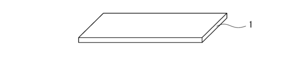
- FIG. 2 is a perspective view showing the shape of a target according to an embodiment of the present invention.
- FIG. 2 is a perspective view showing the shape of a target according to an embodiment of the present invention.
- FIG. 2 is a perspective view showing the shape of a target according to an embodiment of the present invention.
- FIG. 2 is a perspective view showing the shape of a target according to an embodiment of the present invention.
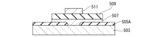
- 1 is a longitudinal cross-sectional view showing a thin film transistor according to an embodiment of the present invention.
- 1 is a longitudinal cross-sectional view showing a thin film transistor according to an embodiment of the present invention.
- FIG. 1 is a vertical cross-sectional view showing a quantum tunnel field effect transistor according to an embodiment of the present invention.
- FIG. 1 is a longitudinal cross-sectional view showing a quantum tunnel field effect transistor according to an embodiment of the present invention.
- FIG. 3 is a longitudinal cross-sectional view showing another embodiment of a quantum tunnel field effect transistor.
- FIG. 3 is a vertical cross-sectional view for explaining the manufacturing procedure of a quantum tunnel field effect transistor.
- FIG. 3 is a vertical cross-sectional view for explaining the manufacturing procedure of a quantum tunnel field effect transistor.
- FIG. 3 is a vertical cross-sectional view for explaining the manufacturing procedure of a quantum tunnel field effect transistor.
- FIG. 3 is a vertical cross-sectional view for explaining the manufacturing procedure of a quantum tunnel field effect transistor.
- FIG. 3 is a vertical cross-sectional view for explaining the manufacturing procedure of a quantum tunnel field effect transistor.
- 1 is a top view showing a display device using a thin film transistor according to an embodiment of the present invention.
- 2 is a diagram showing a circuit of a pixel section that can be applied to a pixel of a VA type liquid crystal display device.
- 1 is a diagram showing a circuit of a pixel portion of a display device using an organic EL element.
- 1 is a diagram showing a circuit of a pixel portion of a solid-state image sensor using a thin film transistor according to an embodiment of the present invention.
- 1 is an X-ray diffraction pattern of the oxide sintered body produced in Example 1.
- 2 is a mapping image of oxygen atoms in the oxide sintered body produced in Example 1.
- film or “thin film” and the term “layer” may be interchanged with each other in some cases.
- the "oxide sintered body” may be simply referred to as the "sintered body”.
- a “sputtering target” may be simply referred to as a "target.”
- electrically connected includes a case where a connection is made via "something that has some kind of electrical effect.”
- something that has some kind of electrical effect is not particularly limited as long as it enables transmission and reception of electrical signals between connected objects.
- something that has some kind of electrical action includes electrodes, wiring, switching elements (such as transistors), resistance elements, inductors, capacitors, and other elements with various functions.
- the functions of the source and drain of a transistor may be interchanged when transistors with different polarities are used or when the direction of current changes during circuit operation. Therefore, in this specification and the like, the terms source and drain can be used interchangeably.
- a numerical range expressed using “ ⁇ ” means a range that includes the numerical value written before “ ⁇ ” as the lower limit and the numerical value written after " ⁇ " as the upper limit. do.
- the present inventors invented the present invention based on the following findings. Cracks that occur during sputtering film formation at high power (high output) are caused by the surface of the sputtering target exposed to high-energy plasma becoming highly heated, and the temperature between the surface of the target and the back surface of the target being cooled. This is thought to be due to the generation of thermal stress due to the difference. Examples of parameters related to the occurrence of cracks include (1) flexural strength, (2) thermal conductivity, (3) coefficient of linear expansion, and (4) Young's modulus.
- the above (2) thermal conductivity, (3) coefficient of linear expansion, and (4) Young's modulus can be improved by changing the crystal structure and the ratio of the constituent crystals. You can change the value to some extent.
- (1) the bending strength can be improved by suppressing pores in the sintered body or reducing the average grain size of the crystal phase. Therefore, in order to improve the crack resistance (hereinafter, this resistance may be referred to as power resistance) when sputtering a film at high power (high output), it is effective to increase the bending strength. It is.
- the present inventors have determined that, in a sputtering target equipped with an oxide sintered body containing In element, Ga element, and O element, the crystal structure contained in the sintered body and the atomic composition ratio of Ga element are Through this study, we obtained the knowledge that sputtering film formation at high output is possible. The present inventors also discovered that in a sputtering target equipped with an oxide sintered body containing an In element, a Ga element, and an O element, the crystal structure contained in the sintered body, the atomic composition ratio of the Ga element, and By examining the average grain size of the crystal structure represented by In 2 O 3 , we have found that it becomes possible to form a film by sputtering at high output and to improve crack resistance.
- the sputtering target according to this embodiment includes a sintered body.
- the sintered body becomes a film raw material when forming a film by sputtering. That is, the sputtering target according to the present embodiment includes an oxide sintered body containing In element, Ga element, and O element.
- the sintered body includes a crystal structure represented by In2O3 , the atomic composition ratio of the Ga element in the oxide sintered body satisfies the following formula (1), and the oxide sintered body
- the bending strength is 140 MPa or more. 8 ⁇ Ga/(In+Ga) ⁇ 20 (1)
- In and Ga represent the number of atoms of indium element and gallium element in the sintered body, respectively.
- the sintered body included in the target according to the present embodiment includes a crystal structure represented by In 2 O 3 .
- the sintered body may include another crystal structure such as GaInO 3 in addition to the crystal structure represented by In 2 O 3 .
- the ratio of the crystal structure represented by In 2 O 3 in the sintered body according to the present embodiment is preferably substantially 80% or more in terms of area ratio. Therefore, the crystal structure represented by In 2 O 3 is preferably the main phase in the sintered body included in the target according to the present embodiment.
- the crystal structure represented by In 2 O 3 is a bixbite phase.
- the ratio of the crystal structure represented by In 2 O 3 in the sintered body is determined by measuring the X-ray diffraction (XRD) of the sintered body, and calculating the peak area of the strongest line of each crystal phase and the RIR value ( Reference Intensity Ratio).
- the crystal phase of the sintered body has a crystal structure represented by In 2 O 3 (i.e., a bixbite phase represented by In 2 O 3 ) and a crystal structure represented by GaInO 3 .
- the ratio of the crystal structure represented by In 2 O 3 is the ratio of the crystal structure represented by In 2 O 3 to the entire crystal structure of the crystal structure represented by In 2 O 3 and the crystal structure represented by GaInO 3 . This is the ratio of the crystal structure represented by O3 .
- the crystal phase of the sintered body when the crystal phase of the sintered body is composed of a crystal structure represented by In 2 O 3 , a crystal structure represented by GaInO 3 , and a crystal structure A described below, In 2
- the ratio of the crystal structure represented by O 3 is the ratio of the crystal structure represented by In 2 O 3 to the entire crystal structure of the crystal structure represented by In 2 O 3, the crystal structure represented by GaInO 3 , and the crystal structure A. is the proportion of crystal structure.
- the average grain size of the crystal structure represented by In 2 O 3 contained in the sintered body is preferably 3 ⁇ m or less. That is, it is preferable that the average grain size of the crystal structure represented by In 2 O 3 as the main phase is 3 ⁇ m or less. If the average grain size of the crystal structure represented by In 2 O 3 contained in the sintered body is 3 ⁇ m or less, the bending strength of the sintered body is improved, and as a result, the power resistance is further improved.
- the average grain size of the crystal structure represented by In 2 O 3 is more preferably 2.5 ⁇ m or less, and even more preferably 2 ⁇ m or less.
- the lower limit of the average grain size of the crystal structure represented by In 2 O 3 is not particularly limited, and may be, for example, 1 ⁇ m or more.
- the crystal structure represented by GaInO 3 is included, for example, in addition to the crystal structure represented by In 2 O 3 contained as the main phase, In It is also conceivable to reduce the average grain size of the crystal structure represented by GaInO 3 instead of the average grain size of the crystal structure represented by 2 O 3 .
- the average grain size of the crystal structure represented by GaInO 3 is made small, it is difficult to obtain excellent flexural strength if the average grain size of the crystal structure represented by In 2 O 3 , which is the main phase, is large. .
- the average grain size of the crystal structure represented by In 2 O 3 can be calculated as follows. First, the polished sintered body is observed using a SEM, and a secondary electron image and a backscattered electron image are observed at a magnification of 2000 times. When observing by SEM, the atomic ratio of each crystal particle is determined using energy dispersive X-ray spectroscopy (EDS). Further, the crystal phase is confirmed by measuring the sintered body by X-ray diffraction (XRD). Next, each crystal phase is identified by comparing it with the crystal structure identified by X-ray diffraction (XRD). The crystal grains are measured using the obtained SEM image, and the average value of the grain size is calculated.
- EDS energy dispersive X-ray spectroscopy
- the average grain size of the crystal structure represented by In 2 O 3 can be measured, for example, as follows. If the planar shape of the sintered body is a square, divide the surface of the sintered body into 16 equal areas, cut out 1 cm squares at 16 center points of each square, and perform mirror polishing. Use as a sample for measurement. The measurement surface of the cut out sintered body is further divided into 9 equal areas, and a secondary electron image and a backscattered electron image are observed at 2000x magnification at 9 center points of each square. During SEM observation, EDS measurement is performed and compared with the crystal structure identified by XRD to identify which crystal each crystal particle is.
- the particle size is measured from the obtained SEM image, and the average value of the particle size of the particles within the frame at nine locations is determined. This operation is performed on measurement samples cut out from 16 locations, and the average value of the particle diameters obtained from a total of 144 SEM images is defined as the average particle diameter.
- the grain size is measured based on JIS R 1670:2006, with the grain size of the crystal grains as equivalent circle diameter. Specifically, as a procedure for measuring the equivalent circle diameter, a circular ruler is applied to the grain to be measured in the microstructure photograph, and the diameter corresponding to the area of the grain to be measured is read. For particles with an aspect ratio of 2 or more, the average value of the longest diameter and the shortest diameter is taken as the particle size of the particle. More specifically, this can be confirmed by the method described in the Examples below.
- the crystal phase of the sintered body has a crystal structure represented by In2O3 , and also has an incident angle (2 ⁇ ) determined by X-ray (CuK ⁇ ray) diffraction measurement.
- the crystal structure A includes a crystal structure A in which diffraction peaks are observed at each of the positions (A) to (E) below.
- the sintered body may further include the above-mentioned crystal structure A as a crystal phase contained in the sintered body. preferable. (A) 28° or more, 29° or less (B) 45° or more, less than 46° (C) 46° or more, less than 47° (D) 47° or more, 48° or less (E) 50° or more, 51° or less
- the crystal phase of the sintered body according to this embodiment includes the crystal structure A, it is possible to change the values of the thermal conductivity, linear expansion coefficient, and Young's modulus of the sintered body, and as a result, Even if the film is formed with high power, cracks are more likely to be suppressed.
- the sintered body included in the target according to the present embodiment has a crystal structure in which the content of O element (oxygen element) is different in the elemental mapping image, and a region where the content of O element (oxygen element) is relatively small. It is preferable that the regions have a relatively high content of O element (oxygen element) and a region with a relatively low content of O element are continuous.
- a structure with a low content of O element that is, a structure with many oxygen defects, has a low resistance value.
- the continuous connection (continuous connection) of this crystal structure with a low O element content makes it possible to keep the resistance value of the entire sintered body low, and as a result, it can be formed with high power. Even with a film, the occurrence of cracks can be more easily suppressed. If the resistance value of the sintered body is high, it may cause abnormal discharge and cause cracks to occur when forming a film at high power (high output).
- the elemental mapping image of the sintered body can be evaluated using a scanning electron microscope (SEM)-energy dispersive X-ray spectroscopy (EDS).
- SEM scanning electron microscope
- EDS energy dispersive X-ray spectroscopy
- the surface roughness Ra (arithmetic mean roughness) of the sintered body is preferably 0.5 ⁇ m or less. Further, the sintered body included in the target according to the present embodiment has a surface roughness Ra (arithmetic mean roughness) of 0.5 ⁇ m or less, and has a ground surface without directionality. is preferred.
- the surface roughness Ra of the sintered body is more preferably less than 0.5 ⁇ m, and even more preferably 0.25 ⁇ m or less.
- the surface roughness Ra of the sintered body included in the target according to this embodiment is 0.5 ⁇ m or less, preferably, the surface roughness Ra of the sintered body included in the target according to this embodiment is 0.5 ⁇ m or less, and If the polishing surface has a non-directional polishing surface, abnormal discharge and generation of particles can be prevented. Further, in the sintered body included in the target according to the present embodiment, it is preferable that the surface roughness Rz (maximum height roughness) of the surface of the sintered body is less than 2.0 ⁇ m. When the surface roughness Rz is less than 2.0 ⁇ m, a sputtering target with improved crack resistance is likely to be obtained. Examples of methods for adjusting the surface roughness Ra and surface roughness Rz of the sintered body include the method described below in the sputtering target manufacturing process.
- the atomic composition ratio of the Ga element satisfies the following formula (1). 8 ⁇ Ga/(In+Ga) ⁇ 20 (1)
- the atomic composition ratio of Ga (Ga/(In+Ga)) expressed by the above formula (1) is 8 or more, Ar gas and O 2 commonly used
- Ar gas and O 2 commonly used
- the thin film immediately after forming from becoming a completely crystalline film and from forming a thin film containing microcrystals in the thin film immediately after forming, and to improve patterning during TFT fabrication.
- generation of residue is suppressed.
- a residue may be generated by etching using a weak acid such as oxalic acid when manufacturing a TFT. , it becomes difficult to obtain the desired TFT characteristics.
- Ga/(In+Ga) is more preferably 10 or more, and even more preferably 12 or more.
- the thin film after being formed may be subjected to high-temperature annealing treatment, laser annealing treatment, etc. Even without special annealing treatment, the thin film after being formed can be easily crystallized by heat treatment (annealing treatment) at about 300° C. to 450° C. Furthermore, the thin film can be made larger without using expensive equipment. If the thin film is insufficiently crystallized after the thin film is annealed, the TFT including the insufficiently crystallized thin film may not be able to secure high mobility and stability.
- Ga/(In+Ga) is more preferably 18 or less, and even more preferably 16 or less.
- the sintered body included in the target according to the present embodiment may substantially consist only of In (indium) element, Ga (gallium) element, and O (oxygen) element.
- substantially means that the sintered body according to the present embodiment does not contain other components within the range where the effects of the present invention resulting from the combination of the In element, Ga element, and O element are produced. It means that it is okay to stay.
- the sintered body included in the target according to the present embodiment the sintered body may contain an element that is an impurity.
- the total content of In element and Ga element is preferably 99 at% or more with respect to the total (100 at%) of the metal elements in the sintered body, and 99 It is more preferably .5 atom % or more, and even more preferably 99.9 atom % or more.
- the total content of In element and Ga element may be 100 atomic % with respect to the total of metal elements in the sintered body. Note that in this specification, atomic % may be expressed as at %.
- Impurities are elements that are not intentionally added and are mixed in raw materials, manufacturing processes, etc. That is, impurities are unavoidable impurities that are inevitably included.
- Examples of impurities include alkali metal elements (elements such as Li (lithium), Na (sodium), K (potassium), and Rb (rubidium)), alkaline earth metal elements (elements such as Mg (magnesium), Ca (calcium), ), Sr (strontium), Ba (barium), etc.), H element (hydrogen element), B element (boron element), C element (carbon element), N element (nitrogen element), F element (fluorine element) , Si element (silicon element), and at least one element selected from the group consisting of Cl element (chlorine element), Zr element (zirconium element), Al element (aluminum element), and Sn element (tin element).
- the sintered body may contain H element (hydrogen element).
- the atomic concentration of the H element in the sintered body is preferably 1 ⁇ 10 16 cm ⁇ 3 or more and less than 1 ⁇ 10 18 cm ⁇ 3 .
- the atomic concentration of H element in the sintered body is more preferably 3 ⁇ 10 16 cm ⁇ 3 or more, and even more preferably 5 ⁇ 10 16 cm ⁇ 3 or more. If the H element concentration in the sintered body is too low, the effect of the H element degassed from the adhesion prevention plate of the sputtering chamber during film formation will be large, and the degassed H element will be mixed unevenly into the formed film.
- the atomic concentration of H element in the sintered body is more preferably 5 ⁇ 10 17 cm ⁇ 3 or less, and even more preferably 3 ⁇ 10 17 cm ⁇ 3 or less. If the concentration of H element in the sintered body is too high, a large amount of H element will be mixed into the formed film, which will form a donor level or acceptor level, and as a result, the reliability of TFT will be greatly deteriorated. It may be easier to connect with what you do.
- the sintered body may contain C element (carbon element).
- the lower limit of the atomic concentration of C in the sintered body is not particularly limited, and the amount of impurities during target production may be 1 ⁇ 10 16 cm ⁇ 3 .
- the atomic concentration of C element is preferably 1 ⁇ 10 16 cm ⁇ 3 or more and less than 1 ⁇ 10 18 cm ⁇ 3 .
- the atomic concentration of the C element in the sintered body is more preferably 7 ⁇ 10 17 cm ⁇ 3 or less, and even more preferably 4 ⁇ 10 17 cm ⁇ 3 or less.
- the atomic concentration of the C element is too high, a large amount of the C element will be mixed into the formed film, which will form a donor level or an acceptor level, resulting in a significant deterioration of the reliability of the TFT. It may be easier to connect.
- the sintered body may contain an H element (hydrogen element) and a C element (carbon element).
- the atomic concentrations of the H element and the C element are both 1 ⁇ 10 16 cm ⁇ 3 or more and less than 1 ⁇ 10 18 cm ⁇ 3 . preferable.
- the unit [atoms/cm 3 ] for the atomic concentration of element H and element C is sometimes expressed as [cm ⁇ 3 ].
- the atomic concentration of H element and C element contained in the sintered body can be determined by secondary ion mass spectrometry (SIMS) measurement.
- SIMS secondary ion mass spectrometry
- a dynamic SIMS device can be used for SIMS measurement.
- the sintered body included in the target according to the present embodiment may contain one or more elements selected from the group consisting of positive trivalent, positive tetravalent, and positive pentavalent elements as long as the effect is not impaired. may contain an element (X element).
- the sputtering target according to the present embodiment includes one or more elements selected from the group consisting of In element, Ga element, O element, and positive trivalent, positive tetravalent, and positive pentavalent.
- the oxide sintered body may include an oxide sintered body containing the X element. Even in this case, in one embodiment, the oxide sintered body includes a crystal structure represented by In 2 O 3 , and the atomic composition ratio of the Ga element in the oxide sintered body is as described above. Formula (1) is satisfied, and the oxide sintered body has a bending strength of 140 MPa or more. Further, the sintered body included in the sputtering target in this embodiment may include a crystal structure represented by GaInO 3 or may include the crystal structure A described above. Furthermore, in the sintered body included in the sputtering target in this embodiment, the average grain size of the crystal structure represented by In 2 O 3 may be 3 ⁇ m or less.
- the additive element X element is, for example, Zn (zinc) element, Mg (magnesium) element, Ti (titanium) element, Fe (iron) element, Zr (zirconium) element, Nb (niobium) element, Hf (hafnium) element.
- the additive element X is at least one of Zn (zinc) element and Sn (tin) element.
- the sintered body included in the sputtering target in this embodiment may substantially consist only of In (indium) element, Ga (gallium) element, O (oxygen) element, and X element. "Substantially" has the same meaning as above.
- the total content of In element, Ga element, and X element is 99 atomic % or more with respect to the total (100 atomic %) of the metal elements in the sintered body.
- the content is preferably 99.5 atom % or more, more preferably 99.9 atom % or more.
- the total content of In element, Ga element, and X element may be 100 atomic % with respect to the total of metal elements in the sintered body.
- the amount of element X which is an additive element, is preferably 2 at% or less, more preferably 1 at% or less, and even more preferably 0.5 at% or less.
- amount of the additive element is 2 at % or less, when a TFT is manufactured using the target according to this embodiment, it is easy to obtain a TFT with high mobility and high stability.
- the amount of added elements increases, the obtained TFT may have problems such as a decrease in mobility and a decrease in stability.
- the amount of element X, which is an additive element is expressed by the following formula (2). 0.02 ⁇ (X/(In+Ga+X))...(2)
- In, Ga, and X represent the number of atoms of indium element, gallium element, and X element in the sintered body, respectively.
- the content (atomic ratio) of each metal element in the sintered body can be determined by measuring the abundance of each element by ICP (Inductive Coupled Plasma) measurement or XRF (X-ray Fluorescence) measurement.
- ICP Inductive Coupled Plasma
- XRF X-ray Fluorescence
- An inductively coupled plasma emission spectrometer can be used for ICP measurement.
- a thin film fluorescent X-ray analyzer can be used for the XRF measurement.
- the density measured by the Archimedes method of the sintered body is 6.3 g/cm 3 or more. It is more preferable that the density of the sintered body measured by the Archimedes method is 6.5 g/cm 3 or more.
- the relative density of the sintered body is preferably 97% or more, more preferably 99% or more.
- Relative density means a percentage of the value obtained by dividing the actual density of the oxide sintered body measured by the Archimedes method by the theoretical density of the oxide sintered body.
- the thickness of the sintered body is usually preferably 2 mm or more and 20 mm or less.
- the thickness of the sintered body is more preferably 3 mm or more, and even more preferably 4 mm or more.
- the thickness of the sintered body is more preferably 12 mm or less, even more preferably 9 mm or less, even more preferably 6 mm or less.
- the sintered body included in the target according to this embodiment has a bending strength of 140 MPa or more.
- the bending strength is preferably 150 MPa or more, more preferably 160 MPa or more.
- the bending strength of the sintered body suppresses the occurrence of cracks when a film is formed by sputtering at high power (high output).
- the bending strength of the sintered body is determined based on JIS R 1601:2008 as the average value of the three-point bending strength measurements of 30 test pieces.
- the sintered body included in the target according to this embodiment also exhibits excellent physical properties such as thermal conductivity, coefficient of linear expansion, and Young's modulus.
- the linear expansion coefficient of the sintered body can be measured in accordance with JIS R 1618:2002 at a measurement temperature of 30° C. to 500° C., a temperature increase rate of 10 K/min, and an air atmosphere.
- the Young's modulus of the sintered body can be measured in accordance with JIS R 1602:1995 using an ultrasonic flaw detector at room temperature in the atmosphere.
- the thermal conductivity of the sintered body is determined by measuring the specific heat capacity by the laser flash method (at room temperature, in vacuum) and by measuring the thermal diffusivity by the laser flash method (at room temperature, in the atmosphere) in accordance with JIS R 1611:2010. Then, the thermal conductivity can be calculated from the following formula (Equation 1).
- ⁇ (thermal conductivity) Cp (specific heat capacity) x ⁇ (density) x ⁇ (thermal diffusivity) ... (Math. 1)
- ⁇ is the density of the oxide sintered body.
- the sputtering target according to this embodiment includes an oxide sintered body and cooling and holding members such as a backing plate provided on the oxide sintered body as necessary.
- the material of the backing plate which is a member for holding and cooling the oxide sintered body, is preferably a material with excellent thermal conductivity such as copper.
- the sintered body provided in the sputtering target according to this embodiment has a bonding surface attached to the holding member, and a bonding surface attached to the holding member. It has a sputtering surface which is a surface opposite to the surface and is sputtered.
- the sputtering surface is a smooth surface (that is, a smooth surface with the above-mentioned surface roughness Ra of 0.5 ⁇ m or less), and the surface opposite to the sputtering surface can be used as the bonding surface. preferable.
- the shape of the sputtering target is not particularly limited.
- the sputtering target may be, for example, plate-shaped as shown by reference numeral 1 in FIG. 1A, or cylindrical as shown by reference numeral 1A in FIG. 1B.
- the planar shape may be rectangular as shown by reference numeral 1 in FIG. 1A, or circular as shown by reference numeral 1B in FIG. 1C.
- the oxide sintered body may be integrally molded, or it may be of a multi-segmented type in which a plurality of divided oxide sintered bodies (symbol 1C) are each fixed to the backing plate 3, as shown in FIG. 1D.
- the method for manufacturing a sputtering target according to the present embodiment preferably includes, for example, the following steps.
- a step of preparing a raw material powder having a particle size of 0.5 ⁇ m or less (hereinafter sometimes referred to as a raw material powder preparation step).
- a step of mixing the raw material powders to obtain a raw material mixture, and then granulating the raw material mixture to obtain a raw material granule (hereinafter sometimes referred to as a granulation step).
- a step of molding the raw material granules to obtain a molded body hereinafter sometimes referred to as a molding step).
- a process of sintering the molded body to obtain a sintered body (hereinafter sometimes referred to as a sintering process).
- a preferable method for manufacturing the target according to the present embodiment further includes a step of heat-treating the sintered body (annealing step), a step of at least grinding the sintered body (hereinafter sometimes referred to as a grinding step), At least one selected from the group consisting of a process of cleaning the compact (hereinafter sometimes referred to as a cleaning process), and a process of bonding the sintered body to a backing plate (hereinafter sometimes referred to as a bonding process). It may have one step.
- raw material powder preparation process raw material powder to be used as a raw material for the sintered body included in the sputtering target according to the present embodiment is prepared.
- the raw material powders prepared in the raw material powder preparation step are indium oxide with an average particle size of 0.5 ⁇ m or less, and gallium oxide with an average particle size of 0.5 ⁇ m or less.
- the raw material powder is, if necessary, a raw material powder of a compound containing one or more elements selected from the group consisting of positive trivalence, positive tetravalence, and positive pentavalence, and having an average particle size of 0.5 ⁇ m or less. You may also prepare.
- the raw material powder may be prepared by obtaining a raw material powder having an average particle size of 0.5 ⁇ m or less, or may be prepared by obtaining a raw material powder having an average particle size of more than 0.5 ⁇ m, and the average particle size of the obtained raw material powder. may be adjusted to 0.5 ⁇ m or less.
- the average particle size of the raw material powder prepared in the raw material powder preparation step is preferably 0.1 ⁇ m or more and 0.5 ⁇ m or less.
- the average particle size of the raw material powder is 0.1 ⁇ m or more, aggregation of the raw material powders is easily suppressed, and the raw material powders can be mixed almost uniformly.
- the average particle size of the raw material powder is 0.5 ⁇ m or less, the average particle size of the crystal structure represented by In 2 O 3 contained in the sintered body after sintering can be easily controlled to 3 ⁇ m or less.
- the average particle size of the raw material powder can be calculated by at least one of the following methods: particle size evaluation using a particle size distribution analyzer and specific surface area determined by the BET method. Further, the average particle size of the raw material powder can also be confirmed using a SEM device.
- the average particle size of the obtained raw material powder exceeds 0.5 ⁇ m, it is preferable to pre-pulverize the raw material powder to adjust the average particle size of the raw material powder to 0.5 ⁇ m or less.
- Preliminary pulverization can be performed using a bead mill, a ball mill, a jet mill, or the like.
- the material of the pot used in preliminary crushing is not particularly limited, and examples thereof include agate, alumina, and the like.
- the material of the grinding media (balls) used in the preliminary grinding is not particularly limited, and examples include materials such as alumina and zirconia.
- the grinding time in preliminary grinding is preferably 30 minutes or more and 6 hours or less.
- the grinding time in the preliminary grinding is 30 minutes or more, a sufficient grinding effect can be obtained and it becomes easier to adjust the average particle size to a predetermined average particle size. If the crushing time in preliminary crushing is 6 hours or less, the material of the pot and the material of the ball will be scraped and it will be difficult for foreign matter to get mixed in (contamination will be difficult to occur). When manufactured, it is easy to obtain a TFT with high mobility and high stability.
- a binder, a dispersant, an antifoaming agent, and the like may be appropriately added to the pulverization, if necessary.
- the raw material powders of indium oxide and gallium oxide prepared in the raw material powder preparation step have high purity.
- the purity of each raw material powder is preferably 99% by mass or more, more preferably 99.9% by mass or more, and even more preferably 99.99% by mass or more.
- the raw material powder when using a raw material powder of a compound containing one or more elements selected from the group consisting of positive trivalent, positive tetravalent, and positive pentavalent, the raw material powder also includes raw material powder of indium oxide and gallium oxide. Similarly, high purity is preferred.
- the purity of the raw material powder of a compound containing one or more elements selected from the group consisting of positive trivalence, positive tetravalence, and positive pentavalence is preferably 99% by mass or more, and 99.9% by mass. % or more, and even more preferably 99.99% by mass or more.
- a high-purity raw material powder is used, a sintered body with a dense structure can be obtained, and the volume resistivity of a sputtering target including the sintered body is reduced.
- a TFT is manufactured using a sputtering target including the sintered body, formation of defect levels due to impurities can be suppressed, and a TFT with high mobility and high stability can be obtained.
- the raw material powders prepared in the raw material powder preparation step described above are mixed to form a mixed raw material powder, and if necessary, a dispersant, a thickener, etc. are added to form a raw material mixture.
- the mixed raw material powder may be used as a raw material mixture as it is.
- the raw material mixture is granulated to obtain raw material granules.
- the raw material granules may be referred to as raw material granulated powder.
- a dispersant to break up the agglomeration and a thickener to adjust the viscosity to be suitable for granulation in a spray dryer are added to the raw material powder prepared in the raw material powder preparation process, and then the raw material powder is added to the raw material powder prepared in the raw material powder preparation process.
- a raw material mixture may be obtained by mixing using a ball mill, bead mill, jet mill, or the like. Among these, the device used for water mixing is preferably a bead mill.
- Using a bead mill allows the raw material powder to be mixed uniformly, which allows sufficient sintering at the sintering temperatures described below, making it easier to obtain a sputtering target that allows sputtering film formation at high power (high output).
- the dispersant include ammonia neutralized acrylic acid methacrylic acid copolymer
- examples of the thickener include polyvinyl alcohol.
- the mixing time of the raw material powders is not particularly limited as long as the raw material powders are sufficiently mixed. It is preferable that the mixing time of the raw material powder is, for example, 2 hours or more and 48 hours or less. When the mixing time is 2 hours or more, the raw material powder is likely to be sufficiently mixed. When the mixing time is 48 hours or less, the occurrence of re-agglomeration of the raw material powder is likely to be suppressed. Further, when the mixing time is 48 hours or less, contamination with foreign substances from the pot material, the ball material, etc. is suppressed.
- the granulation process for granulating the raw material mixture can be performed using a spray dryer or the like.
- the shape of the raw material granules obtained in the granulation step is not particularly limited, and is preferably perfectly spherical in order to uniformly fill the mold in the molding step described below.
- the granulation conditions are appropriately selected by adjusting the concentration of the raw material mixture after mixing the raw material powders introduced into the spray dryer, the rotation speed of the spray dryer, the hot air temperature used for drying, etc.
- the raw material mixture obtained above may be used as it is to prepare the raw material granules.
- the calcined raw material mixture may be prepared into a pulverized raw material mixture again by the method described in the pre-pulverization of the raw material powder and then used.
- the particle size of the raw material granules formed by the granulation process is not particularly limited, and is preferably controlled within a range of, for example, 25 ⁇ m or more and 150 ⁇ m or less.
- the particle size of the raw material granules is 25 ⁇ m or more, the slipperiness of the raw material granules on the surface of the mold used in the molding process described later improves, and the raw material granules can be sufficiently filled into the mold. .
- the particle size of the raw material granules is 150 ⁇ m or less, it is possible to prevent the particle size from being too large and reducing the filling rate in the mold.
- the particle size of the raw material granules is more preferably 25 ⁇ m or more and 75 ⁇ m or less.
- the method for obtaining raw material granules having a particle size within a desired range is not particularly limited.
- a method may be used in which raw material granules that have been subjected to granulation treatment are sieved to select raw material granules that fall within a desired particle size range.
- the sieve used in this method is preferably a sieve having openings large enough to allow raw material granules of a desired particle size to pass through.
- the sieves used in this method include a first sieve for sorting the raw material granules based on the lower limit of the particle size range, and a second sieve for sorting the raw material granules based on the upper limit of the particle size range.
- a sieve is used.
- the size is such that raw material granules of less than 25 ⁇ m can pass through, and raw material granules of 25 ⁇ m or more do not pass.
- a sieve (first sieve) having openings raw material granules having a particle size of 25 ⁇ m or more are selected.
- the raw material granules after sorting are passed through a sieve (second sieve) having an opening size that allows raw material granules of 150 ⁇ m or less to pass through, but does not allow raw material granules of more than 150 ⁇ m to pass through. Then, raw material granules with a size of 25 ⁇ m or more and 150 ⁇ m or less are selected.
- the second sieve may be used first, and then the first sieve may be used.
- the method for controlling the particle size range of the raw material granules is not limited to the method using a sieve as described above, and any method may be used as long as the raw material granules to be subjected to the molding process can be controlled within a desired range.
- the raw material granules are molded by a method such as die press molding, cast molding, or injection molding to obtain a molded body.
- a method such as die press molding, cast molding, or injection molding to obtain a molded body.
- CIP cold isostatic pressing
- sintering process In the sintering process, a sintered body is obtained by sintering the molded body obtained in the molding process. In the sintering process, a commonly used sintering method such as pressureless sintering, hot press sintering, or hot isostatic pressing (HIP) sintering can be used. The obtained sintered body becomes a sputtering target material.
- a commonly used sintering method such as pressureless sintering, hot press sintering, or hot isostatic pressing (HIP) sintering can be used.
- the obtained sintered body becomes a sputtering target material.
- the sintering temperature is preferably 1300°C or higher and 1400°C or lower.
- the sintering temperature is 1300° C. or higher, the sintering of the molded body sufficiently progresses, thereby suppressing the generation of a large number of pores in the sintered body, and easily improving the bending strength.
- the sintering temperature is 1400° C. or less, the average grain size of the crystal structure represented by In 2 O 3 contained in the sintered body can be easily controlled to a range of 3 ⁇ m or less, and the bending strength can be easily improved.
- the sintering time is preferably 12 hours or more and 48 hours or less.
- the sintering time is 12 hours or more, the sintering of the molded body sufficiently progresses, thereby suppressing the generation of a large number of pores in the sintered body, and easily improving the bending strength.
- the sintering time is 48 hours or less, the average grain size of the crystal structure represented by In 2 O 3 contained in the sintered body can be easily controlled to a range of 3 ⁇ m or less, and the bending strength can be easily improved.
- the rate of temperature increase from room temperature to the sintering temperature is not particularly limited, and is preferably 0.1° C./min or more and 3° C./min or less.
- the temperature may be maintained at 700° C. or more and 800° C. or less for 1 hour or more and 10 hours or less, and after being maintained at a predetermined temperature for a predetermined time, the temperature may be raised to the sintering temperature.
- Examples of the atmosphere during sintering include an atmosphere of air or oxygen gas, an atmosphere containing air or oxygen gas and a reducing gas, or an atmosphere containing air or oxygen gas and an inert gas.
- Examples of the reducing gas include hydrogen gas, methane gas, and carbon monoxide gas.
- Examples of the inert gas include argon gas and nitrogen gas.
- the obtained sintered body is annealed.
- the annealing step is a step provided as necessary.
- the sintered body is usually treated at a holding temperature of 700° C. or higher and 1100° C. or lower, and for a holding time of 1 hour or more and 5 hours or less.
- the sintered body may be once cooled and then the temperature may be raised again for annealing, or the sintered body may be annealed when the temperature is lowered from the sintering temperature.
- Examples of the atmosphere during annealing include an atmosphere of air or oxygen gas, an atmosphere containing air or oxygen gas and a reducing gas, or an atmosphere containing air or oxygen gas and an inert gas.
- Examples of the reducing gas include hydrogen gas, methane gas, and carbon monoxide gas.
- Examples of the inert gas include argon gas and nitrogen gas.
- the obtained sintered body is cut into an appropriate shape, and the surface of the oxide sintered body is polished. Specifically, the sintered body is cut into a shape suitable for attachment to a sputtering device, and the surface of the oxide sintered body is polished.
- the abrasive grain size of the grindstone used in the grinding process is preferably 100 ⁇ m or less. If the abrasive grain size of the grindstone is 100 ⁇ m or less, cracking of the sintered body can be prevented.
- the grindstone used in the grinding process is preferably a diamond grindstone.
- the grinding depth in the grinding step is preferably 0.3 mm or more, more preferably 0.5 mm or more, and even more preferably 2 mm or more. By grinding the surface of the sintered body by 0.3 mm or more, the portion where the crystal structure fluctuates near the surface can be removed.
- the surface of the sintered body that has undergone the grinding process preferably has a surface roughness Ra (arithmetic mean roughness) of 5 ⁇ m or less.
- the surface of the sintered body that has undergone the grinding process preferably has a surface roughness Rz (maximum height roughness) of less than 2.0 ⁇ m. Further, it is preferable that the surface of the sintered body subjected to the grinding process has a surface roughness Ra (arithmetic mean roughness) of 5 ⁇ m or less and has a ground surface without directionality.
- the sputtered surface of the sintered body may be further mirror-finished.
- known polishing techniques such as mechanical polishing, chemical polishing, and mechanochemical polishing (combination of mechanical polishing and chemical polishing) can be used.
- the polishing method is not limited to these methods.
- the cleaning process In the cleaning process, the sintered body ground in the grinding process is cleaned.
- the cleaning treatment include air blowing and running water washing. When removing foreign matter by air blowing, it is possible to remove the foreign matter more effectively by using a dust collector to draw air from the opposite side of the air blow nozzle.
- ultrasonic cleaning or the like in addition to the cleaning treatment by air blowing or running water cleaning, ultrasonic cleaning or the like may be further performed.
- An effective method for ultrasonic cleaning is to perform multiple oscillations at a frequency of 25 kHz or more and 300 kHz or less. For example, it is preferable to perform ultrasonic cleaning by multiplexing 12 different frequencies at 25 kHz intervals between 25 kHz and 300 kHz.
- the bonding process is a process of bonding the sintered body after the processing process to the backing plate with a low melting point metal (for example, metal indium, metal gallium, etc.).
- a low melting point metal for example, metal indium, metal gallium, etc.
- the bonding rate is preferably 90% or more, more preferably 95% or more, and even more preferably 98% or more.
- the bonding ratio here indicates the area ratio of the surface where the target material and the target support material are bonded via the bonding layer to the area of the surface where the target material and the target support material overlap.
- the bonding rate can be confirmed by, for example, X-ray computed tomography (CT) or ultrasonic flaw detection.
- the sputtering target according to this embodiment since a target having the same atomic composition as the sintered body according to the present embodiment is used, the TFT obtained by sputtering has high mobility and high stability. is obtained.
- the crystalline oxide thin film according to this embodiment is a crystalline oxide thin film using the sputtering target according to this embodiment.
- the crystalline oxide thin film according to this embodiment is obtained by forming a film using the sputtering target according to this embodiment.
- the crystalline oxide thin film according to the present embodiment is produced by, for example, a step of forming an oxide thin film by sputtering using the sputtering target according to the present embodiment (hereinafter sometimes referred to as an oxide thin film deposition step). It is preferable that the oxide film be obtained by a manufacturing method including a step of subjecting an oxide thin film to a heat treatment (hereinafter sometimes referred to as a heat treatment step).
- a heat treatment step a manufacturing method including a step of subjecting an oxide thin film to a heat treatment
- the crystalline oxide thin film according to this embodiment is a crystalline oxide thin film.
- the crystalline oxide thin film according to this embodiment is an amorphous oxide thin film after sputtering film formation and before heat treatment (annealing treatment), and crystallinity is improved by annealing treatment after sputtering film formation. As a result, a crystalline oxide thin film is obtained. Since the crystalline oxide thin film according to this embodiment is a crystalline oxide thin film, a thin film transistor (TFT) including the crystalline oxide thin film according to this embodiment has high mobility and high stability. .
- TFT thin film transistor
- Whether the oxide thin film is amorphous or crystalline can be confirmed by X-ray diffraction (XRD) measurement of each oxide thin film.
- XRD X-ray diffraction
- a gas that does not substantially contain impurity gases is used.
- one or more gases selected from the group consisting of argon, hydrogen, and oxygen, which do not substantially contain impurity gases are used as the sputtering gas.
- the sputtering gas is preferably a mixed gas of argon and oxygen that does not substantially contain impurity gases.
- Sputtering gas "substantially does not contain any impurity gases” means that it does not contain argon, hydrogen, gases that cannot be eliminated (unavoidable impurity gases) such as adsorbed water introduced by gas insertion, chamber leaks, and adsorbed gases. This means that impurity gases other than oxygen are not actively introduced.
- the sputtering gas for example, a commercially available mixed gas of high purity argon and high purity oxygen can be used. Impurities are preferably excluded from the sputter gas if possible.
- the proportion of impurity gas in the sputtering gas is preferably 0.1% by volume or less, more preferably 0.05% by volume or less. If the proportion of impurity gas is 0.1% by volume or less, crystallization of the oxide thin film will proceed without any problem.
- the purity of high-purity argon and high-purity oxygen is preferably 99% by volume or more, more preferably 99.9% by volume or more, and even more preferably 99.99% by volume or more.
- the partial pressure of oxygen in the mixed gas of argon and oxygen which is the sputtering gas, is preferably in the range of 0% to 50% by volume, more preferably in the range of 5% to 30% by volume. If the oxygen partial pressure is within the above range, it will easily crystallize and become a semiconductor upon heating. By changing the oxygen partial pressure, the degree of oxidation of the obtained thin film, that is, the degree of crystallization, can be adjusted.
- the oxygen partial pressure may be appropriately selected as necessary.
- the heat treatment temperature for crystallizing the amorphous thin film after deposition is preferably in the range of 300°C to 450°C, more preferably 300°C to 350°C. If the heat treatment temperature is 300° C. or higher, the oxide thin film can be easily crystallized. When the heat treatment temperature is 450° C. or lower, abnormal growth of crystals and enlargement of crystal grains can be suppressed.
- the heat treatment time for crystallizing the amorphous thin film after film formation is preferably 0.1 hours or more and 5 hours or less, and preferably 0.3 hours or more and 3 hours or less. is more preferable, and even more preferably 0.5 hours or more and 2 hours or less. If the heat treatment time is 0.1 hour or more, crystallization will not occur and the oxide thin film will easily crystallize. If the heat treatment time is 5 hours or less, it is economical.
- the temperature increase rate is preferably 2° C./min or more and 40° C./min or less, more preferably 3° C./min or more and 20° C./min or less. If the temperature increase rate in the heat treatment step is 2° C./min or more, the production efficiency of the oxide thin film will be improved compared to the case where it is less than 1° C./min. If the temperature increase rate in the heat treatment step is 40° C./min or less, metal elements can be uniformly diffused during crystallization, and crystals in which metal is not segregated at grain boundaries can be formed.
- the crystalline oxide thin film according to this embodiment can also be applied to various integrated circuits such as logic circuits, memory circuits, and differential amplifier circuits, and can be applied to electronic devices and the like. Further, the crystalline oxide thin film according to this embodiment can be used in some layers of solar cells, liquid crystal elements, organic electroluminescent elements, inorganic electroluminescent elements, micro organic EL displays, micro LED (Light Emitting Diode) displays, and It can be applied as a part of a layer of a display device such as a mini LED display.
- the crystalline oxide thin film according to this embodiment can be used for solid-state imaging devices, X-ray sensors, power semiconductor devices, touch panels, LSIs (Large Scale Integrated circuits), resistance change memories, DRAMs (Dynamic Random Access Memory), and dielectric It can be applied as part of layers of memory, BEOL (Back End of Line), and microprocessors.
- the crystalline oxide thin film according to this embodiment can be used in semiconductor layers of field effect transistors, electrostatic induction transistors, quantum tunnel field effect transistors, Schottky barrier transistors, Schottky diodes, PN diodes, and resistance elements, and , they can also be adapted as some layers.
- Examples of the thin film transistor according to this embodiment include a thin film transistor including a crystalline oxide thin film according to this embodiment.
- the crystalline oxide thin film according to this embodiment is preferably an oxide semiconductor thin film.
- the crystalline oxide thin film according to this embodiment is preferable to use as a channel layer of a thin film transistor.
- the thin film transistor according to this embodiment has the crystalline oxide thin film according to this embodiment as a channel layer
- other element configurations in the thin film transistor are not particularly limited, and known element configurations can be adopted.
- the thin film transistor according to this embodiment can be suitably used in electronic devices. Specifically, the thin film transistor according to this embodiment can be suitably used in display devices such as liquid crystal displays and organic EL displays.
- the thickness of the channel layer in the thin film transistor according to this embodiment is usually 10 nm or more and 300 nm or less, preferably 20 nm or more and 250 nm or less.
- the channel layer in the thin film transistor according to this embodiment is normally used in an N-type region, but it can be used in a PN junction in combination with various P-type semiconductors such as a P-type Si-based semiconductor, a P-type oxide semiconductor, and a P-type organic semiconductor. It can be used for various semiconductor devices such as type transistors.
- the thin film transistor according to this embodiment can also be applied to various integrated circuits such as field effect transistors, logic circuits, memory circuits, and differential amplifier circuits. Furthermore, in addition to field effect transistors, the present invention can also be applied to electrostatic induction transistors, Schottky barrier transistors, Schottky diodes, and resistive elements. That is, the thin film transistor according to this embodiment can be applied to the applications exemplified in "Applications of Thin Film Transistors" described later.
- the structure of the thin film transistor according to this embodiment can be selected from known structures such as bottom gate, bottom contact, top gate, and top contact without any limitation.
- the thin film transistor according to this embodiment can be suitably used in a display device.
- the thin film transistor 100 includes a silicon wafer 20, a gate insulating film 30, an oxide thin film 40, a source electrode 50, a drain electrode 60, and interlayer insulating films 70 and 70A.
- the silicon wafer 20 is a gate electrode.
- the gate insulating film 30 is an insulating film that blocks conduction between the gate electrode and the oxide thin film 40, and is provided on the silicon wafer 20.
- the oxide thin film 40 is a channel layer and is provided on the gate insulating film 30.
- the crystalline oxide thin film according to this embodiment is used as the oxide thin film 40.
- the source electrode 50 and the drain electrode 60 are conductive terminals for allowing source current and drain current to flow through the oxide thin film 40, and are each provided so as to be in contact with both ends of the oxide thin film 40.
- the interlayer insulating film 70 is an insulating film that blocks electrical conduction between the source electrode 50 and drain electrode 60 and the oxide thin film 40 except for the contact portions.
- the interlayer insulating film 70A is an insulating film that blocks electrical conduction between the source electrode 50 and drain electrode 60 and the oxide thin film 40 except for the contact portions.
- the interlayer insulating film 70A is also an insulating film that blocks electrical conduction between the source electrode 50 and the drain electrode 60.
- the interlayer insulating film 70A is also a channel layer protective layer.
- the structure of the thin film transistor 100A is similar to that of the thin film transistor 100, except that a source electrode 50 and a drain electrode 60 are provided in contact with both the gate insulating film 30 and the oxide thin film 40. are different. Another difference is that an interlayer insulating film 70B is integrally provided so as to cover the gate insulating film 30, the oxide thin film 40, the source electrode 50, and the drain electrode 60.
- the materials for forming the drain electrode 60, the source electrode 50, and the gate electrode can be arbitrarily selected.
- a silicon wafer is used as the substrate, and the silicon wafer also acts as an electrode, but the electrode material is not limited to silicon.
- transparent electrodes such as indium tin oxide (ITO), indium zinc oxide (IZO), ZnO, and SnO2 , metal electrodes such as Al, Ag, Cu, Cr, Ni, Mo, Au, Ti, and Ta, Alternatively, metal electrodes or laminated electrodes made of alloys containing these can be used.
- the gate electrode may be formed on a substrate such as glass.
- interlayer insulating films 70, 70A, and 70B there is no particular restriction on the material for forming the interlayer insulating films 70, 70A, and 70B, and any commonly used material can be selected arbitrarily.
- materials for forming the interlayer insulating films 70, 70A, and 70B for example, compounds represented by MO x , MN x , and MN and y is a real number exceeding 0. The same applies to x and y in the compounds exemplified below.) Specifically, compounds such as SiO 2 , SiO x , SiN x , and SiN x O y can be used as the material.
- the materials include, for example, Al 2 O 3 , Ta 2 O 5 , TiO 2 , MgO, ZrO 2 , CeO 2 , K 2 O, Li 2 O, Na 2 O, Rb 2 O, Sc 2 O 3 , Compounds such as Y2O3 , HfO2 , CaHfO3, PbTiO3 , BaTa2O6 , SrTiO3 , Sm2O3 , and AlN can also be used.
- the valences of the anions (oxygen anions and nitrogen anions) in these oxide compounds and nitride compounds are not particularly limited, and may be real numbers greater than zero.
- the thin film transistor according to this embodiment is a back channel etch type (bottom gate type)
- a protective film on the drain electrode, source electrode, and channel layer.
- durability can be easily improved even when the TFT is driven for a long time.
- a gate insulating film is formed on a channel layer.
- the protective film or insulating film can be formed, for example, by CVD, but this may involve a process using high temperatures. Further, the protective film or the insulating film often contains impurity gas immediately after film formation, and therefore it is preferable to perform heat treatment (annealing treatment). By removing impurity gases through heat treatment, a stable protective film or insulating film can be obtained, making it easier to form a highly durable TFT element.
- the crystalline oxide thin film according to this embodiment it becomes less susceptible to the effects of temperature in the CVD process and subsequent heat treatment, so even when a protective film or insulating film is formed, the TFT characteristics stability can be improved.
- On/Off characteristics are a factor that determines the display performance of a display.
- the On/Off ratio is preferably 6 digits or more.
- the On current is important because of current drive, but the On/Off ratio is preferably 6 digits or more.
- the thin film transistor according to this embodiment preferably has an On/Off ratio of 1 ⁇ 10 6 or more.
- the mobility of the TFT according to this embodiment is preferably 5 cm 2 /Vs or more, and preferably 10 cm 2 /Vs or more.
- the saturation mobility is determined from the transfer characteristics when a drain voltage of 20V is applied. Specifically, it can be calculated by creating a graph of the transfer characteristic Id-Vg, calculating the transconductance (Gm) of each Vg, and finding the saturation mobility using the saturation region formula.
- Id is the current between the source and drain electrodes
- Vg is the gate voltage when voltage Vd is applied between the source and drain electrodes.
- the threshold voltage (Vth) is preferably -3.0V or more and 3.0V or less, more preferably -2.0V or more and 2.0V or less, and even more preferably -1.0V or more and 1.0V or less.
- the threshold voltage (Vth) is ⁇ 3.0 V or higher, a thin film transistor with high mobility can be obtained.
- the threshold voltage (Vth) is 3.0 V or less, a thin film transistor with a small off-state current and a large on-off ratio can be obtained.
- the On/Off ratio is preferably 10 6 or more and 10 12 or less, more preferably 10 7 or more and 10 11 or less, and even more preferably 10 8 or more and 10 10 or less.
- the On/Off ratio is 10 6 or more, a liquid crystal display can be driven.
- the On/Off ratio is 10 12 or less, an organic EL with high contrast can be driven.
- the On/Off ratio is 10 12 or less
- the off current can be reduced to 10 -11 A or less
- the image retention time can be extended, Sensitivity can be improved.
- the crystalline oxide thin film according to this embodiment can also be used in a quantum tunnel field effect transistor (FET).
- FET quantum tunnel field effect transistor
- the quantum tunnel field effect transistor may be referred to as a quantum tunnel field effect transistor.
- FIG. 4 shows a schematic diagram (vertical cross-sectional view) of a quantum tunnel field effect transistor (FET) according to one embodiment.
- the quantum tunnel field effect transistor 501 includes a p-type semiconductor layer 503, an n-type semiconductor layer 507, a gate insulating film 509, a gate electrode 511, a source electrode 513, and a drain electrode 515.
- the p-type semiconductor layer 503, the n-type semiconductor layer 507, the gate insulating film 509, and the gate electrode 511 are stacked in this order.
- Source electrode 513 is provided on p-type semiconductor layer 503.
- Drain electrode 515 is provided on n-type semiconductor layer 507.
- the p-type semiconductor layer 503 is a p-type group IV semiconductor layer, and here is a p-type silicon layer.
- the n-type semiconductor layer 507 here is the n-type oxide thin film according to the above embodiment.
- the source electrode 513 and the drain electrode 515 are conductive films.
- an insulating layer may be formed on the p-type semiconductor layer 503.
- the p-type semiconductor layer 503 and the n-type semiconductor layer 507 are connected through a contact hole, which is a region formed by partially opening an insulating layer.
- the quantum tunnel field effect transistor 501 may include an interlayer insulating film covering its upper surface.
- the quantum tunnel field effect transistor 501 is a quantum tunnel field effect transistor that performs current switching in which the current tunneling through the energy barrier formed by the p-type semiconductor layer 503 and the n-type semiconductor layer 507 is controlled by the voltage of the gate electrode 511. (FET).
- FET field effect transistor
- FIG. 5 shows a schematic diagram (vertical cross-sectional view) of a quantum tunnel field effect transistor 501A according to another embodiment.
- the configuration of quantum tunnel field effect transistor 501A is similar to quantum tunnel field effect transistor 501, except that a silicon oxide layer 505 is formed between p-type semiconductor layer 503 and n-type semiconductor layer 507.
- the presence of the silicon oxide layer allows the off-state current to be reduced.
- the thickness of the silicon oxide layer 505 is preferably 10 nm or less. By setting the thickness of the silicon oxide layer 505 to 10 nm or less, it is possible to prevent tunneling current from flowing, difficulty in forming an energy barrier, and changes in barrier height, thereby reducing tunneling current. , prevent changes.
- the thickness of the silicon oxide layer 505 is preferably 8 nm or less, more preferably 5 nm or less, still more preferably 3 nm or less, and even more preferably 1 nm or less.
- the n-type semiconductor layer 507 is an n-type oxide semiconductor.
- the oxide thin film constituting the n-type semiconductor layer 507 may be amorphous. Since the oxide thin film constituting the n-type semiconductor layer 507 is amorphous, it can be etched with organic acids such as oxalic acid, and the difference in etching speed with other layers becomes large, making it difficult to etch metal layers such as wiring. Etching can be performed well without any adverse effects.
- the oxide thin film constituting the n-type semiconductor layer 507 may be crystalline. Since the oxide thin film constituting the n-type semiconductor layer 507 is crystalline, the band gap becomes larger than in the case of an amorphous film, and the off-state current can be reduced. Since the work function can also be increased, it becomes easier to control the current tunneling through the energy barrier formed by the p-type group IV semiconductor material and the n-type semiconductor layer 507.
- the method for manufacturing the quantum tunnel field effect transistor 501 is not particularly limited, but the following method can be exemplified.
- an insulating film 505A is formed on the p-type semiconductor layer 503, and a contact hole 505B is formed by opening a part of the insulating film 505A by etching or the like.
- an n-type semiconductor layer 507 is formed on the p-type semiconductor layer 503 and the insulating film 505A. At this time, the p-type semiconductor layer 503 and the n-type semiconductor layer 507 are connected via the contact hole 505B.
- a gate insulating film 509 and a gate electrode 511 are formed in this order on the n-type semiconductor layer 507.
- an interlayer insulating film 519 is provided to cover the insulating film 505A, the n-type semiconductor layer 507, the gate insulating film 509, and the gate electrode 511.
- a contact hole 519A is formed by opening a part of the insulating film 505A on the p-type semiconductor layer 503 and the interlayer insulating film 519, and a source electrode 513 is provided in the contact hole 519A.
- a contact hole 519B is formed by opening part of the gate insulating film 509 and interlayer insulating film 519 on the n-type semiconductor layer 507, and a drain electrode 515 is formed in the contact hole 519B.
- the quantum tunnel field effect transistor 501 can be manufactured by the above procedure.
- the quantum tunnel field effect transistor 501A can be manufactured.
- the thin film transistor according to this embodiment is preferably a channel doped thin film transistor.
- a channel-doped thin film transistor is a transistor in which carriers in the channel are properly controlled by n-type doping, rather than by oxygen vacancies, which tend to fluctuate in response to external stimuli such as atmosphere and temperature, resulting in high mobility and high reliability. Compatible effects can be obtained.
- the thin film transistor according to this embodiment can be suitably used in solar cells, display elements (liquid crystal elements, organic electroluminescent elements, inorganic electroluminescent elements, etc.), and power semiconductor elements.
- the thin film transistor according to the present embodiment can be used in display devices (liquid crystal displays, organic EL (electro luminescence) displays, micro organic EL displays, micro LED (light emitting diode) displays, mini LED displays, etc.), solid-state image sensors, touch panels, etc.
- the present invention can be suitably used as a transistor in a device using an active matrix method.
- the thin film transistor according to this embodiment can also be applied to various integrated circuits such as field effect transistors, logic circuits, memory circuits, and differential amplifier circuits, and can be applied to electronic devices and the like.
- the electronic device according to this embodiment preferably includes a thin film transistor.
- the thin film transistor according to this embodiment can be applied not only to field effect transistors but also to static induction transistors and Schottky barrier transistors.
- the thin film transistor according to this embodiment can also be applied as a transistor for sensors such as image sensors, X-ray sensors, and biological sensors.
- FIG. 7A is a top view of the display device according to this embodiment.
- FIG. 7B is a circuit diagram for explaining a circuit of a pixel section when a liquid crystal element is applied to the pixel section of the display device according to this embodiment.
- FIG. 7C is a circuit diagram for explaining a circuit of a pixel section when an organic EL element is applied to the pixel section of the display device according to this embodiment.
- the thin film transistor according to this embodiment can be used as the transistor arranged in the pixel portion. Since the thin film transistor according to this embodiment can easily be an n-channel type, a part of the drive circuit that can be configured with an n-channel transistor is formed on the same substrate as the transistor of the pixel portion. By using the thin film transistor described in this embodiment in the pixel portion and the driver circuit, a highly reliable display device can be provided.
- FIG. 7A An example of a top view of an active matrix display device is shown in FIG. 7A.
- a pixel portion 301, a first scanning line driving circuit 302, a second scanning line driving circuit 303, and a signal line driving circuit 304 are formed on a substrate 300 of the display device.
- a plurality of signal lines are arranged extending from a signal line driving circuit 304, and a plurality of scanning lines are arranged extending from a first scanning line driving circuit 302 and a second scanning line driving circuit 303.
- Pixels each having a display element are provided in a matrix in the intersection area of the scanning line and the signal line.
- the substrate 300 of the display device is connected to a timing control circuit (also referred to as a controller or control IC) via a connection portion such as an FPC (Flexible Printed Circuit).
- a timing control circuit also referred to as a controller or control IC
- FPC Flexible Printed Circuit
- the first scanning line driving circuit 302, the second scanning line driving circuit 303, and the signal line driving circuit 304 are formed on the same substrate 300 as the pixel portion 301. Therefore, the number of externally provided components such as drive circuits is reduced, so that costs can be reduced. Further, when a drive circuit is provided outside the substrate 300, it becomes necessary to extend the wiring, and the number of connections between the wirings increases. When the drive circuits are provided on the same substrate 300, the number of connections between the wirings can be reduced, and reliability or yield can be improved.
- FIG. 7B an example of the circuit configuration of a pixel is shown in FIG. 7B.
- a circuit of a pixel section that can be applied to a pixel section of a VA type liquid crystal display device is shown.
- This circuit of the pixel portion can be applied to a configuration in which one pixel has multiple pixel electrodes. Each pixel electrode is connected to a different transistor, and each transistor is configured to be driven by a different gate signal. Thereby, signals applied to individual pixel electrodes of pixels designed in a multi-domain can be independently controlled.
- the gate wiring 312 of the transistor 316 and the gate wiring 313 of the transistor 317 are separated so that different gate signals can be applied to them.
- a source or drain electrode 314 that functions as a data line is commonly used by the transistor 316 and the transistor 317.
- the thin film transistors according to this embodiment can be used as the transistors 316 and 317. Thereby, a highly reliable liquid crystal display device can be provided.
- a first pixel electrode is electrically connected to the transistor 316, and a second pixel electrode is electrically connected to the transistor 317.
- the first pixel electrode and the second pixel electrode are separated.
- the shapes of the first pixel electrode and the second pixel electrode are not particularly limited.
- the first pixel electrode may have a V-shape.
- the gate electrode of the transistor 316 is connected to the gate wiring 312, and the gate electrode of the transistor 317 is connected to the gate wiring 313.
- the operation timings of the transistor 316 and the transistor 317 can be made different, thereby controlling the orientation of the liquid crystal.
- a storage capacitor may be formed by the capacitor wiring 310, a gate insulating film functioning as a dielectric, and a capacitor electrode electrically connected to the first pixel electrode or the second pixel electrode.
- the multi-domain structure includes a first liquid crystal element 318 and a second liquid crystal element 319 in one pixel.
- the first liquid crystal element 318 is composed of a first pixel electrode, a counter electrode, and a liquid crystal layer therebetween
- the second liquid crystal element 319 is composed of a second pixel electrode, a counter electrode, and a liquid crystal layer therebetween.
- the pixel portion is not limited to the configuration shown in FIG. 7B.
- a switch, a resistive element, a capacitive element, a transistor, a sensor, or a logic circuit may be added to the pixel portion shown in FIG. 7B.
- FIG. 7C Another example of the pixel circuit configuration is shown in FIG. 7C.
- the structure of a pixel portion of a display device using organic EL elements is shown.
- FIG. 7C is a diagram showing an example of an applicable circuit of the pixel section 320.
- an example is shown in which two n-channel transistors are used in one pixel.
- the crystalline oxide thin film according to this embodiment can be used for a channel formation region of an n-channel transistor.
- Digital time gradation driving can be applied to the circuit of the pixel section.
- the thin film transistor according to this embodiment can be used as the switching transistor 321 and the driving transistor 322. Thereby, a highly reliable organic EL display device can be provided.
- the configuration of the circuit of the pixel portion is not limited to the configuration shown in FIG. 7C.
- a switch, a resistive element, a capacitive element, a sensor, a transistor, or a logic circuit may be added to the circuit of the pixel portion shown in FIG. 7C.
- the above is a description of the case where the thin film transistor according to this embodiment is used in a display device.
- a CMOS (complementary metal oxide semiconductor) image sensor is a solid-state imaging device that holds a potential in a signal charge storage section and outputs the potential to a vertical output line via an amplification transistor.
- a CMOS image sensor When there is a leakage current in a reset transistor and/or a transfer transistor included in a CMOS image sensor, charging or discharging occurs due to the leakage current, and the potential of the signal charge storage section changes.
- the potential of the signal charge storage section changes, the potential of the amplification transistor also changes, resulting in a value that deviates from the original potential, and the captured image deteriorates.
- the amplification transistor may be either a thin film transistor or a bulk transistor.
- FIG. 8 is a diagram showing an example of a pixel configuration of a CMOS image sensor.
- a pixel is composed of a photodiode 3002 which is a photoelectric conversion element, a transfer transistor 3004, a reset transistor 3006, an amplification transistor 3008, and various wirings, and a plurality of pixels are arranged in a matrix to form a sensor.
- a selection transistor electrically connected to the amplification transistor 3008 may be provided.
- "OS” written in the transistor symbol indicates an oxide semiconductor (Oxide Semiconductor), and "Si" indicates silicon, which represent materials that are preferable when applied to each transistor. The same applies to subsequent drawings.
- the photodiode 3002 is connected to the source side of the transfer transistor 3004, and a signal charge accumulation section 3010 (FD: also referred to as floating diffusion) is formed on the drain side of the transfer transistor 3004.
- the source of the reset transistor 3006 and the gate of the amplification transistor 3008 are connected to the signal charge storage section 3010 .
- the reset power line 3110 can be deleted.
- the crystal oxide thin film according to this embodiment may be used for the photodiode 3002, and the same material as the oxide thin film used for the transfer transistor 3004 and the reset transistor 3006 may be used.
- the prepared In 2 O 3 raw material powder and the pre-pulverized Ga 2 O 3 raw material powder were mixed to obtain a mixed raw material powder, and then acrylic acid methacrylate was added to this mixed raw material powder as a dispersant.
- Acid copolymer ammonia neutralized product manufactured by Sanmei Kasei Co., Ltd., Banstar A raw material mixture was obtained.
- the obtained raw material mixture was supplied to a spray dryer and granulated at a rotation speed of 12,000 rpm and a hot air temperature of 150° C. to obtain a raw material granulated powder.
- the raw material granulated powder is passed through a 100 mesh sieve to remove raw material granulated powder with a particle size of more than 150 ⁇ m, and then the raw material granulated powder is passed through a 500 mesh sieve to remove raw material granulated powder with a particle size of less than 25 ⁇ m.
- the particle size of the raw material granulated powder was adjusted to a range of 25 ⁇ m or more and 150 ⁇ m or less.
- the raw material granulated powder after adjusting the particle size was uniformly filled into a mold with an inner diameter of 300 mm x 600 mm x 9 mm, and pressure molded using a cold press machine. After pressure molding, molding was carried out at a pressure of 294 MPa using a cold isostatic press device (CIP device) to obtain a molded body.
- CIP device cold isostatic press device
- the three obtained sintered bodies were each cut and surface ground to obtain three oxide sintered bodies measuring 142 mm x 305 mm x 5 mm.
- One of these sheets was used for characteristic evaluation, and two sheets were used for a G1 target [142 mm x 610 mm (divided into 2) x 5 mmt].
- the oxide sintered body was surface ground using a surface grinder using a diamond grindstone having a grindstone grain size of 80 ⁇ m.
- the surface grinding processing conditions are as follows.
- a diamond grinding wheel with an abrasive grain size of 40 ⁇ m After grinding under the above surface grinding conditions, a diamond grinding wheel with an abrasive grain size of 40 ⁇ m, then a diamond grinding wheel with an abrasive grain size of 20 ⁇ m, and a grinding wheel with a fine abrasive grain size are sequentially used under the above surface grinding conditions. Grinding was done.
- a G1 target was manufactured by bonding the two obtained oxide sintered plates (142 mm x 305 mm x 5 mm) to a backing plate made of Cu (copper).
- the plane ground surface is used as the sputtering surface
- the surface opposite to the sputtering surface is used as the bonding surface
- the bonding of the oxide sintered body plate is performed.
- the surface side was bonded to the backing plate.
- the bonding rate was 98% or higher for all targets.
- Example 3 Example 4
- ZnO with an average particle size of 0.8 ⁇ m and SnO 2 with an average particle size of 0.4 ⁇ m were prepared as raw material powders, and the powders shown in Tables 1 and 2 were prepared. It was weighed to obtain the atomic composition ratio (at%).
- ZnO was pre-pulverized under the same conditions as Ga 2 O 3 .
- the average particle size of ZnO after preliminary crushing was 0.32 ⁇ m.
- a sintered body was obtained in the same manner as in Example 1 except for the above. Thereafter, the obtained sintered body was ground and bonded in the same manner as in Example 1 to be used as a sputtering target, and evaluated in the same manner as in Example 1.
- Comparative example 1 to comparative example 3 First, the same In 2 O 3 and Ga 2 O 3 as in Example 1 were prepared as raw material powders and weighed so as to have the atomic composition ratios (at%) shown in Table 3. In Comparative Examples 1 to 3, the raw material powders were not premixed. The raw material powders were then mixed in a planetary ball mill for 4 hours. The raw material powders after mixing were dried and classified to obtain a raw material mixture. The obtained raw material mixture was molded in the same manner as in Example 1. Three compacts were made, and the three obtained compacts were heated to 780°C in an oxygen atmosphere in a sintering furnace, held at 780°C for 5 hours, and further heated to 1400°C.
- the sintering temperature (1400°C) was maintained for 20 hours. Thereafter, it was cooled in a furnace to obtain an oxide sintered body. Note that the temperature increase rate was 2° C./min. Thereafter, it was ground and bonded in the same manner as in Example 1 to obtain a sputtering target, and evaluated in the same manner as in Example 1.
- XRD Measurement and Identification of Crystal Phase The obtained sintered body was subjected to XRD measurement using an X-ray diffraction measuring device to investigate the crystal structure.
- the measurement conditions for the above X-ray diffraction measurement (XRD) are as follows. Equipment: D8 DISCOVER Plus (Bruker Japan Co., Ltd.) X-ray: CuK ⁇ (1.5418 ⁇ )
- the crystal grain size was measured as follows. The surface of the sintered body produced in the same batch as the sputtering target was divided into 16 equal area sections, and 16 center points of each square were cut out to form 1 cm squares. The cut out sputtering target was embedded in resin and mirror-polished using a polishing device (manufactured by Buehler). After the surface was coated with osmium to make it conductive, it was placed in a scanning electron microscope (SEM) device (manufactured by Hitachi High-Tech), and the measurement surface was further divided into 9 equal areas, and 9 points were measured at the center of each square.
- SEM scanning electron microscope
- a secondary electron image and a backscattered electron image were observed at a magnification of 2000 times. Furthermore, EDS measurement was performed during the SEM measurement to determine the atomic ratio of each crystal grain. The crystal structure of each crystal particle was identified by comparing it with the crystal structure identified by XRD. The particle size was measured from the obtained SEM image, and the average value of the particle size of the particles within the frame at nine locations was determined. This operation was performed for each sample cut out from 16 locations, and the average value of the particle sizes obtained from a total of 144 SEM images was defined as the average particle size. For particles with an aspect ratio of less than 2, the grain size of the crystal grain was measured as the equivalent circle diameter based on JIS R1670:2006.
- a circular ruler is applied to the grain to be measured in the microstructure photograph, and the diameter corresponding to the area of the grain to be measured is read.
- the average value of the longest diameter and the shortest diameter was taken as the particle size of the particle.
- the actual density of the sintered body was measured by the Archimedes method. Specifically, it was measured using water at room temperature.
- Power resistance is the maximum value expressed as sputtering power that does not cause cracks in the sputtering target. After discharging sputtering power at DC 1.5 kW for 1 hour, the chamber was opened and the presence or absence of cracks was visually observed. Thereafter, the sputtering power was increased to 1.75 kW, and after discharging at this sputtering power for 1 hour, the chamber was opened and the presence or absence of cracks was visually observed.
- This operation was performed by increasing the sputtering power in steps of 0.25 kW to check for cracks until cracks were confirmed in the sputtering target.
- the maximum power at which no cracking was observed was taken as an index of power resistance. Note that since sputtering power varies depending on the apparatus, the value obtained by dividing the input power by the target area was standardized as the power density.
- the evaluation conditions for power resistance are as follows.
- FIG. 9 shows an X-ray diffraction pattern of the sintered body used in the target produced in Example 1.
- the sintered body obtained in Example 1 has an incident angle (2 ⁇ ) of (A) 28° or more, 29° or less, ( B) 45° or more and less than 46°, (C) 46° or more and less than 47°, (D) 47° or more and 48° or less, and (E) 50° or more and 51° or less. I understand what is shown. Therefore, it can be seen that the sintered body obtained in Example 1 includes crystal structure A.
- FIG. 10 shows a mapping image of oxygen atoms in the sintered body used in the target produced in Example 1. As shown in FIG. 10, it can be seen that the regions where the content of O element is relatively low are continuous. In FIG. 10, the relatively black portions indicate regions where the content of O element is relatively low.
- Oxide thin film (Example 1 to Example 6 and Comparative Example 1 to Comparative Example 6) Using the sputtering targets prepared in Examples 1 to 6 and Comparative Examples 1 to 6, a metal mask was formed on a silicon wafer with a 100 nm thermal oxide film (gate insulating film) by sputtering. A 40 nm thick oxide thin film (oxide semiconductor thin film layer) was formed through the film. At this time, sputtering was performed using high-purity argon and high-purity oxygen gases as sputtering gases. In addition, a sample in which only a 40 nm thick oxide thin film layer was formed on a glass substrate was simultaneously manufactured under the same conditions. As the glass substrate, ABC-G manufactured by Nippon Electric Glass Co., Ltd. was used.
- 1, 1A, 1B, 1C oxide sintered body, 3: backing plate, 20: silicon wafer, 30: gate insulating film, 40: oxide thin film, 50: source electrode, 60: drain electrode, 70: interlayer insulation film, 70A: interlayer insulating film, 70B: interlayer insulating film, 100: thin film transistor, 100A: thin film transistor, 300: substrate, 301: pixel section, 302: first scanning line drive circuit, 303: second scanning line drive circuit , 304: signal line drive circuit, 310: capacitor wiring, 312: gate wiring, 313: gate wiring, 314: drain electrode, 316: transistor, 317: transistor, 318: first liquid crystal element, 319: second liquid crystal Element, 320: Pixel section, 321: Switching transistor, 322: Drive transistor, 3002: Photodiode, 3004: Transfer transistor, 3006: Reset transistor, 3008: Amplification transistor, 3010: Signal charge storage section, 3100: Power line , 3110: Reset power supply line, 3120: Vertical
Abstract
Provided is a spattering target (1) comprising an oxide sintered compact including an In element, a Ga element, and an O element. Said sintered compact includes a crystal structure represented by In2O3, the atomic composition ratio of the Ga element in the oxide sintered compact satisfies expression (1), and the flexural strength of the oxide sintered compact is 140 MPa or greater. Expression (1): 8 ≤ Ga/(In+Ga) ≤ 20
Description
本発明は、スパッタリングターゲット、スパッタリングターゲットの製造方法、結晶酸化物薄膜、薄膜トランジスタ、及び電子機器に関する。
The present invention relates to a sputtering target, a method for manufacturing a sputtering target, a crystalline oxide thin film, a thin film transistor, and an electronic device.
近年、薄膜トランジスタ(以下、TFTと称する場合がある。)のチャネル層として、多結晶シリコン薄膜、及びアモルファスシリコン薄膜などに加えて、InGaZnOのようなアモルファスの酸化物半導体が使用されるようになってきた。酸化物半導体は、アモルファスシリコンのような大面積均一性が可能であることが特徴である。また、酸化物半導体は、10cm2/Vs以上の移動度が得られ、アモルファスシリコン以上の移動度を持つことが特徴である。
In recent years, in addition to polycrystalline silicon thin films and amorphous silicon thin films, amorphous oxide semiconductors such as InGaZnO have come to be used as channel layers of thin film transistors (hereinafter sometimes referred to as TFTs). Ta. Oxide semiconductors are characterized by the possibility of large area uniformity like amorphous silicon. Further, an oxide semiconductor is characterized in that it can obtain a mobility of 10 cm 2 /Vs or more, and has a mobility higher than that of amorphous silicon.
しかしながら、アモルファス酸化物薄膜において、キャリアの供給源は酸素欠損であり、熱などの外的因子に対して電子の振る舞いが必ずしも安定しないことに起因して、薄膜トランジスタの動作が不安定になるという問題がある。また、可視光照射下で薄膜トランジスタに負バイアスを連続的に印加すると、閾値電圧が負側にシフトする(光負バイアス劣化)現象が生じる、という問題もある。このため、近年、アモルファス酸化物薄膜ではなく、結晶質の酸化物薄膜を、薄膜トランジスタのチャネル層に適用する研究が進められている。
However, in amorphous oxide thin films, the source of carriers is oxygen vacancies, and the behavior of electrons is not necessarily stable in response to external factors such as heat, resulting in unstable operation of thin film transistors. There is. Furthermore, if a negative bias is continuously applied to a thin film transistor under visible light irradiation, there is a problem in that the threshold voltage shifts to the negative side (photonegative bias deterioration). For this reason, in recent years, research has been underway to apply a crystalline oxide thin film, rather than an amorphous oxide thin film, to the channel layer of a thin film transistor.
特許文献1には、ガリウムの含有量がGa/(In+Ga)原子数比で0.15を超えて0.45以下であり、結晶相がビックスバイト型構造のIn2O3相のみによって構成される、結晶質の酸化物薄膜が記載されている。また、特許文献1に記載される酸化物薄膜は、酸化インジウムと酸化ガリウムからなる原料によって得られた酸化物焼結体を含むスパッタリングターゲットを用いて成膜し、エッチング加工、アニール処理することによって得られる。そして、特許文献1には、前記酸化物薄膜をチャネル材料として用いたTFTが記載されている。さらに、特許文献1に記載されるような組成範囲を選択することにより、特殊な成膜方法を使用しなくても、王水等の強酸ではなくシュウ酸などの一般的な弱酸で、エッチング可能な膜を得られることが記載されている。
Patent Document 1 discloses that the gallium content is more than 0.15 and less than 0.45 in Ga/(In+Ga) atomic ratio, and the crystal phase is composed only of In 2 O 3 phase with a bixbite structure. Crystalline oxide thin films have been described. Further, the oxide thin film described in Patent Document 1 is formed using a sputtering target containing an oxide sintered body obtained from raw materials consisting of indium oxide and gallium oxide, and is then etched and annealed. can get. Patent Document 1 describes a TFT using the oxide thin film as a channel material. Furthermore, by selecting the composition range as described in Patent Document 1, etching can be performed with a general weak acid such as oxalic acid instead of a strong acid such as aqua regia without using a special film formation method. It has been described that a film with a similar shape can be obtained.
特許文献2には、インジウムとガリウムを酸化物として含有する酸化物焼結体が記載されている。この酸化物焼結体は、ビックスバイト型構造のIn2O3相が主たる結晶相となり、その中にβ-Ga2O3型構造のGaInO3相、又はGaInO3相と(Ga,In)2O3相が平均粒径5μm以下の結晶粒として微細に分散しており、ガリウムの含有量がGa/(In+Ga)原子数比で10原子%以上35原子%未満である。また、特許文献2に記載される酸化物焼結体から得られるスパッタリングターゲットが記載されている。
Patent Document 2 describes an oxide sintered body containing indium and gallium as oxides. This oxide sintered body has an In 2 O 3 phase with a bixbite type structure as the main crystal phase, and therein, a GaInO 3 phase with a β-Ga 2 O 3 type structure, or a GaInO 3 phase with a (Ga,In) type structure. The 2 O 3 phase is finely dispersed as crystal grains with an average grain size of 5 μm or less, and the gallium content is 10 at % or more and less than 35 at % in Ga/(In+Ga) atomic ratio. Moreover, a sputtering target obtained from an oxide sintered body described in Patent Document 2 is described.
特許文献3には、結晶構造が、実質的にビックスバイト構造を示す酸化インジウムからなる酸化物焼結体が記載されている。当該酸化物焼結体は、前記酸化インジウムにガリウム原子が固溶しており、原子比Ga/(Ga+In)が0.10~0.15である。また、特許文献3に記載される酸化物焼結体から得られるスパッタリングターゲットが記載されている。
Patent Document 3 describes an oxide sintered body made of indium oxide whose crystal structure substantially shows a bixbite structure. In the oxide sintered body, gallium atoms are solidly dissolved in the indium oxide, and the atomic ratio Ga/(Ga+In) is 0.10 to 0.15. Moreover, a sputtering target obtained from an oxide sintered body described in Patent Document 3 is described.
さらに、特許文献2及び特許文献3には、スパッタリングターゲットを適切な結晶相となるように制御することによりノジュールを抑制することや異常放電を防止できることが記載されている。
Further, Patent Document 2 and Patent Document 3 describe that nodules can be suppressed and abnormal discharge can be prevented by controlling the sputtering target to have an appropriate crystal phase.
TFTの製造工程では、生産性の向上、及びTFTの安定性向上を目的として、スパッタリング成膜するときに、高いパワー(高出力)で成膜したいというニーズがある。しかし、高いパワーでスパッタリング成膜を実施すると、成膜中に異常放電(いわゆるアーキング)が発生しやすくなる。さらにスパッタリングターゲット表面が、高エネルギーのプラズマにさらされて高熱になる。そのため、スパッタリングターゲットの表面と冷却されている裏面との間で温度差が生じ、この温度差によって熱応力が発生する。その結果として、スパッタリングターゲットにクラックが発生してしまうという場合がある。
In the TFT manufacturing process, there is a need to perform film formation with high power (high output) when sputtering film formation for the purpose of improving productivity and improving TFT stability. However, when sputtering film formation is performed with high power, abnormal discharge (so-called arcing) tends to occur during film formation. Furthermore, the surface of the sputtering target is exposed to high-energy plasma and becomes extremely hot. Therefore, a temperature difference occurs between the front surface of the sputtering target and the cooled back surface, and this temperature difference generates thermal stress. As a result, cracks may occur in the sputtering target.
従来のスパッタリングターゲットにおいて、高パワーでスパッタリング成膜するときに生じるクラック発生に関する検討は十分ではなく、スパッタリングターゲットは、さらなる改善の余地があった。
In conventional sputtering targets, cracks that occur during high-power sputtering film formation have not been sufficiently studied, and there is room for further improvement in sputtering targets.
本発明の目的は、高いパワー(高出力)でのスパッタリング成膜が可能であるスパッタリングターゲット、当該スパッタリングターゲットの製造方法、当該スパッタリングターゲットを用いた結晶酸化物薄膜、当該結晶酸化物薄膜を含む薄膜トランジスタ、及び当該薄膜トランジスタを含む電子機器を提供することである。
The objects of the present invention are a sputtering target capable of sputtering film formation at high power (high output), a method for manufacturing the sputtering target, a crystalline oxide thin film using the sputtering target, and a thin film transistor including the crystalline oxide thin film. , and an electronic device including the thin film transistor.
[1]
In元素、Ga元素、及びO元素を含む酸化物焼結体を備えるスパッタリングターゲットであって、
前記酸化物焼結体が、In2O3で表される結晶構造を含み、
前記酸化物焼結体中の前記Ga元素の原子組成比が下記式(1)を満たし、
前記酸化物焼結体の抗折強度が140MPa以上である、
スパッタリングターゲット。
8≦Ga/(In+Ga)≦20 ・・・(1) [1]
A sputtering target comprising an oxide sintered body containing In element, Ga element, and O element,
The oxide sintered body includes a crystal structure represented by In2O3 ,
The atomic composition ratio of the Ga element in the oxide sintered body satisfies the following formula (1),
The oxide sintered body has a bending strength of 140 MPa or more,
sputtering target.
8≦Ga/(In+Ga)≦20 (1)
[2]
前記In2O3で表される結晶構造の平均粒径が、3μm以下である、
[1]に記載のスパッタリングターゲット。 [2]
The average grain size of the crystal structure represented by In 2 O 3 is 3 μm or less,
The sputtering target described in [1].
前記In2O3で表される結晶構造の平均粒径が、3μm以下である、
[1]に記載のスパッタリングターゲット。 [2]
The average grain size of the crystal structure represented by In 2 O 3 is 3 μm or less,
The sputtering target described in [1].
[3]
アルキメデス法による実測密度が、6.3g/cm3以上である、
[1]又は[2]に記載のスパッタリングターゲット。 [3]
The actual density measured by the Archimedes method is 6.3 g/cm 3 or more,
The sputtering target according to [1] or [2].
アルキメデス法による実測密度が、6.3g/cm3以上である、
[1]又は[2]に記載のスパッタリングターゲット。 [3]
The actual density measured by the Archimedes method is 6.3 g/cm 3 or more,
The sputtering target according to [1] or [2].
[4]
前記酸化物焼結体が、GaInO3で表される結晶構造を含む、
[1]から[3]のいずれか一項に記載のスパッタリングターゲット。 [4]
The oxide sintered body includes a crystal structure represented by GaInO 3 .
The sputtering target according to any one of [1] to [3].
前記酸化物焼結体が、GaInO3で表される結晶構造を含む、
[1]から[3]のいずれか一項に記載のスパッタリングターゲット。 [4]
The oxide sintered body includes a crystal structure represented by GaInO 3 .
The sputtering target according to any one of [1] to [3].
[5]
前記酸化物焼結体が、さらに、X線(CuKα線)回折測定により入射角(2θ)が、下記(A)~下記(E)の各位置に回折ピークが観測される結晶構造Aを含む、
[1]から[4]のいずれか一項に記載のスパッタリングターゲット。
(A)28°以上、29°以下
(B)45°以上、46°未満
(C)46°以上、47°未満
(D)47°以上、48°以下
(E)50°以上、51°以下 [5]
The oxide sintered body further includes a crystal structure A in which diffraction peaks are observed at each of the following positions (A) to (E) at an incident angle (2θ) according to X-ray (CuKα ray) diffraction measurement. ,
The sputtering target according to any one of [1] to [4].
(A) 28° or more, 29° or less (B) 45° or more, less than 46°
(C) 46° or more and less than 47° (D) 47° or more and 48° or less (E) 50° or more and 51° or less
[6]
[1]から[5]のいずれか一項に記載のスパッタリングターゲットの製造方法であって、
粒径が0.5μm以下である原料粉末を準備する工程と、
前記原料粉末を混合して原料混合物を得た後、前記原料混合物を造粒して、原料造粒物を得る工程と、
前記原料造粒物を成形して成形体を得る工程と、
前記成形体を焼結して前記酸化物焼結体を得る工程と、を有する、
スパッタリングターゲットの製造方法。 [6]
The method for manufacturing a sputtering target according to any one of [1] to [5],
A step of preparing raw material powder having a particle size of 0.5 μm or less;
After mixing the raw material powders to obtain a raw material mixture, granulating the raw material mixture to obtain raw material granules;
a step of molding the raw material granules to obtain a molded body;
sintering the molded body to obtain the oxide sintered body;
A method of manufacturing a sputtering target.
[7]
[1]から[5]のいずれか一項に記載のスパッタリングターゲットを用いた結晶酸化物薄膜。 [7]
A crystalline oxide thin film using the sputtering target according to any one of [1] to [5].
[1]から[5]のいずれか一項に記載のスパッタリングターゲットを用いた結晶酸化物薄膜。 [7]
A crystalline oxide thin film using the sputtering target according to any one of [1] to [5].
[8]
[7]に記載の結晶酸化物薄膜を含む薄膜トランジスタ。 [8]
A thin film transistor comprising the crystalline oxide thin film according to [7].
[7]に記載の結晶酸化物薄膜を含む薄膜トランジスタ。 [8]
A thin film transistor comprising the crystalline oxide thin film according to [7].
[9]
[8]に記載の薄膜トランジスタを含む電子機器。 [9]
An electronic device including the thin film transistor according to [8].
[8]に記載の薄膜トランジスタを含む電子機器。 [9]
An electronic device including the thin film transistor according to [8].
本発明の一態様によれば、高いパワー(高出力)でのスパッタリング成膜が可能であるスパッタリングターゲット、当該スパッタリングターゲットの製造方法、当該スパッタリングターゲットを用いた結晶酸化物薄膜、当該結晶酸化物薄膜を含む薄膜トランジスタ、及び当該薄膜トランジスタを含む電子機器が提供できる。
According to one aspect of the present invention, a sputtering target capable of sputtering film formation at high power (high output), a method for manufacturing the sputtering target, a crystalline oxide thin film using the sputtering target, and the crystalline oxide thin film A thin film transistor including the thin film transistor and an electronic device including the thin film transistor can be provided.
以下、実施の形態について図面等を参照しながら説明する。但し、実施の形態は多くの異なる態様で実施することが可能であり、趣旨及びその範囲から逸脱することなくその形態及び詳細を様々に変更し得ることは当業者であれば容易に理解される。従って、本発明は、以下の実施の形態の記載内容に限定して解釈されない。
Hereinafter, embodiments will be described with reference to the drawings and the like. However, those skilled in the art will readily understand that the embodiments can be implemented in many different ways and that the form and details can be changed in various ways without departing from the spirit and scope of the invention. . Therefore, the present invention should not be interpreted as being limited to the contents described in the following embodiments.
図面において、大きさ、層の厚さ及び領域等は、明瞭化のために誇張されている場合がある。よって、本発明は、図示された大きさ、層の厚さ及び領域等に限定されない。なお、図面は、理想的な例を模式的に示したものであり、本発明は、図面に示す形状及び値等に限定されない。
In the drawings, sizes, layer thicknesses, regions, etc. may be exaggerated for clarity. Therefore, the invention is not limited to the dimensions, layer thicknesses, areas, etc. illustrated. Note that the drawings schematically show ideal examples, and the present invention is not limited to the shapes, values, etc. shown in the drawings.
本明細書にて用いる「第1」、「第2」、「第3」という序数詞は、構成要素の混同を避けるために付されており、数的に特定する旨の記載が無い構成要素については、数的に限定されない。
The ordinal numbers "first," "second," and "third" used in this specification are used to avoid confusion between constituent elements, and refer to constituent elements that are not specified numerically. is not limited in number.
本明細書等において、「膜」又は「薄膜」という用語と、「層」という用語とは、場合によっては、互いに入れ替えることが可能である。
In this specification and the like, the term "film" or "thin film" and the term "layer" may be interchanged with each other in some cases.
本明細書等の焼結体及び酸化物薄膜において、「化合物」という用語と、「結晶相」という用語は、場合によっては、互いに入れ替えることが可能である。
In the sintered body and oxide thin film in this specification, etc., the term "compound" and the term "crystalline phase" can be interchanged with each other depending on the case.
本明細書において、「酸化物焼結体」を単に「焼結体」と称する場合がある。
本明細書において、「スパッタリングターゲット」を単に「ターゲット」と称する場合がある。 In this specification, the "oxide sintered body" may be simply referred to as the "sintered body".
In this specification, a "sputtering target" may be simply referred to as a "target."
本明細書において、「スパッタリングターゲット」を単に「ターゲット」と称する場合がある。 In this specification, the "oxide sintered body" may be simply referred to as the "sintered body".
In this specification, a "sputtering target" may be simply referred to as a "target."
本明細書等において、「電気的に接続」には、「何らかの電気的作用を有するもの」を介して接続されている場合が含まれる。ここで、「何らかの電気的作用を有するもの」は、接続対象間での電気信号の授受を可能とするものであれば、特に制限を受けない。例えば、「何らかの電気的作用を有するもの」には、電極、配線、スイッチング素子(トランジスタなど)、抵抗素子、インダクタ、キャパシタ、及びその他の各種機能を有する素子などが含まれる。
In this specification, etc., "electrically connected" includes a case where a connection is made via "something that has some kind of electrical effect." Here, "something that has some kind of electrical effect" is not particularly limited as long as it enables transmission and reception of electrical signals between connected objects. For example, "something that has some kind of electrical action" includes electrodes, wiring, switching elements (such as transistors), resistance elements, inductors, capacitors, and other elements with various functions.
本明細書等において、トランジスタが有するソースやドレインの機能は、異なる極性のトランジスタを採用する場合又は回路動作において電流の方向が変化する場合などには入れ替わることがある。このため、本明細書等においては、ソースやドレインの用語は、入れ替えて用いることができる。
In this specification and the like, the functions of the source and drain of a transistor may be interchanged when transistors with different polarities are used or when the direction of current changes during circuit operation. Therefore, in this specification and the like, the terms source and drain can be used interchangeably.
本明細書において、「~」を用いて表される数値範囲は、「~」の前に記載される数値を下限値とし、「~」の後に記載される数値を上限値として含む範囲を意味する。
In this specification, a numerical range expressed using "~" means a range that includes the numerical value written before "~" as the lower limit and the numerical value written after "~" as the upper limit. do.
本発明者らは、下記の知見に基づいて本発明を発明した。
高パワー(高出力)でスパッタリング成膜したときに発生するクラックは、高エネルギーのプラズマにさらされたスパッタリングターゲットの表面が高熱になり、ターゲットの表面と、冷却されているターゲットの裏面との温度差により、熱応力が発生することに起因すると考えられる。クラックの発生と関連するパラメータとしては、例えば、(1)抗折強度、(2)熱伝導率、(3)線膨張係数、及び(4)ヤング率などが挙げられる。 The present inventors invented the present invention based on the following findings.
Cracks that occur during sputtering film formation at high power (high output) are caused by the surface of the sputtering target exposed to high-energy plasma becoming highly heated, and the temperature between the surface of the target and the back surface of the target being cooled. This is thought to be due to the generation of thermal stress due to the difference. Examples of parameters related to the occurrence of cracks include (1) flexural strength, (2) thermal conductivity, (3) coefficient of linear expansion, and (4) Young's modulus.
上記の(2)熱伝導率、(3)線膨張係数、及び(4)ヤング率は、例えば、結晶構造を変化させる、及び、構成する結晶の比率を変更する、ことによっても、これら物性の値を多少は変化させることができる。一方、(1)抗折強度は、焼結体中の空孔を抑制したり、結晶相の平均粒径を小さくすることによって、向上させることが可能である。このため、高パワー(高出力)でスパッタリング成膜したときのクラック耐性(以下、この耐性を、パワー耐性と称する場合がある。)を向上させるためには、抗折強度を高くすることが有効である。
The above (2) thermal conductivity, (3) coefficient of linear expansion, and (4) Young's modulus can be improved by changing the crystal structure and the ratio of the constituent crystals. You can change the value to some extent. On the other hand, (1) the bending strength can be improved by suppressing pores in the sintered body or reducing the average grain size of the crystal phase. Therefore, in order to improve the crack resistance (hereinafter, this resistance may be referred to as power resistance) when sputtering a film at high power (high output), it is effective to increase the bending strength. It is.
以上に鑑み、本発明者らは、In元素、Ga元素、及びO元素を含む酸化物焼結体を備えるスパッタリングターゲットにおいて、焼結体に含まれる結晶構造と、Ga元素の原子組成比とを検討することによって、高出力でのスパッタリング成膜が可能になるという知見を得た。
また、本発明者らは、In元素、Ga元素、及びO元素を含む酸化物焼結体を備えるスパッタリングターゲットにおいて、焼結体に含まれる結晶構造と、Ga元素の原子組成比と、さらに、In2O3で表される結晶構造の平均粒径とを検討することによって、高出力でのスパッタリング成膜が可能になるとともに、クラック耐性の向上が可能になるという知見を得た。 In view of the above, the present inventors have determined that, in a sputtering target equipped with an oxide sintered body containing In element, Ga element, and O element, the crystal structure contained in the sintered body and the atomic composition ratio of Ga element are Through this study, we obtained the knowledge that sputtering film formation at high output is possible.
The present inventors also discovered that in a sputtering target equipped with an oxide sintered body containing an In element, a Ga element, and an O element, the crystal structure contained in the sintered body, the atomic composition ratio of the Ga element, and By examining the average grain size of the crystal structure represented by In 2 O 3 , we have found that it becomes possible to form a film by sputtering at high output and to improve crack resistance.
[スパッタリングターゲット]
本実施形態に係るスパッタリングターゲットは、焼結体を備える。当該焼結体は、スパッタリングで成膜するときの膜原料になる。すなわち、本実施形態に係るスパッタリングターゲットは、In元素、Ga元素、及びO元素を含む酸化物焼結体を備える。前記焼結体が、In2O3で表される結晶構造を含み、前記酸化物焼結体中の前記Ga元素の原子組成比が下記式(1)を満たし、前記酸化物焼結体の抗折強度が140MPa以上である。
8≦Ga/(In+Ga)≦20 ・・・(1) [Sputtering target]
The sputtering target according to this embodiment includes a sintered body. The sintered body becomes a film raw material when forming a film by sputtering. That is, the sputtering target according to the present embodiment includes an oxide sintered body containing In element, Ga element, and O element. The sintered body includes a crystal structure represented by In2O3 , the atomic composition ratio of the Ga element in the oxide sintered body satisfies the following formula (1), and the oxide sintered body The bending strength is 140 MPa or more.
8≦Ga/(In+Ga)≦20 (1)
式(1)中、InおよびGaは、それぞれ、焼結体中のインジウム元素およびガリウム元素の原子数を表す。
In formula (1), In and Ga represent the number of atoms of indium element and gallium element in the sintered body, respectively.
<焼結体の結晶粒径>
本実施形態に係るターゲットが備える焼結体において、焼結体は、In2O3で表される結晶構造を含む。当該焼結体は、In2O3で表される結晶構造の他にGaInO3などの別の結晶構造を含んでもよい。 <Crystal grain size of sintered body>
In the sintered body included in the target according to the present embodiment, the sintered body includes a crystal structure represented by In 2 O 3 . The sintered body may include another crystal structure such as GaInO 3 in addition to the crystal structure represented by In 2 O 3 .
本実施形態に係る焼結体におけるIn2O3で表される結晶構造の割合は、面積率で、実質的に80%以上であることが好ましい。したがって、In2O3で表される結晶構造は、本実施形態に係るターゲットが備える焼結体において、主相であることが好ましい。In2O3で表される結晶構造は、ビックスバイト相である。焼結体におけるIn2O3で表される結晶構造の割合は、焼結体のX線回折(XRD:X-ray Diffraction)測定を実施し、各結晶相最強線のピーク面積とRIR値(Reference
Intensity Ratio)から定量した。 The ratio of the crystal structure represented by In 2 O 3 in the sintered body according to the present embodiment is preferably substantially 80% or more in terms of area ratio. Therefore, the crystal structure represented by In 2 O 3 is preferably the main phase in the sintered body included in the target according to the present embodiment. The crystal structure represented by In 2 O 3 is a bixbite phase. The ratio of the crystal structure represented by In 2 O 3 in the sintered body is determined by measuring the X-ray diffraction (XRD) of the sintered body, and calculating the peak area of the strongest line of each crystal phase and the RIR value ( Reference
Intensity Ratio).
焼結体の一態様として、焼結体の結晶相が、In2O3で表される結晶構造(すなわち、In2O3で表されるビックスバイト相)、及びGaInO3で表される結晶構造から構成される場合、In2O3で表される結晶構造の割合は、In2O3で表される結晶構造、及びGaInO3で表される結晶構造の全体の結晶構造に対する、In2O3で表される結晶構造の割合である。
焼結体の一態様として、焼結体の結晶相が、In2O3で表される結晶構造、GaInO3で表される結晶構造、及び後述の結晶構造Aから構成される場合、In2O3で表される結晶構造の割合は、In2O3で表される結晶構造、GaInO3で表される結晶構造、及び結晶構造Aの全体の結晶構造に対する、In2O3で表される結晶構造の割合である。 In one embodiment of the sintered body, the crystal phase of the sintered body has a crystal structure represented by In 2 O 3 (i.e., a bixbite phase represented by In 2 O 3 ) and a crystal structure represented by GaInO 3 . structure, the ratio of the crystal structure represented by In 2 O 3 is the ratio of the crystal structure represented by In 2 O 3 to the entire crystal structure of the crystal structure represented by In 2O 3 and the crystal structure represented by GaInO 3 . This is the ratio of the crystal structure represented by O3 .
In one embodiment of the sintered body, when the crystal phase of the sintered body is composed of a crystal structure represented by In 2 O 3 , a crystal structure represented by GaInO 3 , and a crystal structure A described below, In 2 The ratio of the crystal structure represented by O 3 is the ratio of the crystal structure represented by In 2 O 3 to the entire crystal structure of the crystal structure represented by In 2O 3, the crystal structure represented by GaInO 3 , and the crystal structure A. is the proportion of crystal structure.
焼結体の一態様として、焼結体の結晶相が、In2O3で表される結晶構造、GaInO3で表される結晶構造、及び後述の結晶構造Aから構成される場合、In2O3で表される結晶構造の割合は、In2O3で表される結晶構造、GaInO3で表される結晶構造、及び結晶構造Aの全体の結晶構造に対する、In2O3で表される結晶構造の割合である。 In one embodiment of the sintered body, the crystal phase of the sintered body has a crystal structure represented by In 2 O 3 (i.e., a bixbite phase represented by In 2 O 3 ) and a crystal structure represented by GaInO 3 . structure, the ratio of the crystal structure represented by In 2 O 3 is the ratio of the crystal structure represented by In 2 O 3 to the entire crystal structure of the crystal structure represented by In 2
In one embodiment of the sintered body, when the crystal phase of the sintered body is composed of a crystal structure represented by In 2 O 3 , a crystal structure represented by GaInO 3 , and a crystal structure A described below, In 2 The ratio of the crystal structure represented by O 3 is the ratio of the crystal structure represented by In 2 O 3 to the entire crystal structure of the crystal structure represented by In 2
本実施形態に係るターゲットが備える焼結体において、焼結体に含まれるIn2O3で表される結晶構造の平均粒径は、3μm以下であることが好ましい。つまり、主相であるIn2O3で表される結晶構造の平均粒径が、3μm以下であることが好ましい。焼結体に含まれるIn2O3で表される結晶構造の平均粒径が3μm以下であれば、焼結体の抗折強度が向上し、結果としてパワー耐性がより向上する。In2O3で表される結晶構造の平均粒径は、2.5μm以下であることがより好ましく、2μm以下であることがさらい好ましい。
In2O3で表される結晶構造の平均粒径の下限値は、特に限定されず、例えば、1μm以上であることが挙げられる。
なお、本実施形態に係るターゲットが備える焼結体の一態様において、主相として含むIn2O3で表される結晶構造以外に、例えば、GaInO3で表される結晶構造を含む場合、In2O3で表される結晶構造の平均粒径ではなく、GaInO3で表される結晶構造の平均粒径を小さくすることも考えられる。しかし、GaInO3で表される結晶構造の平均粒径を小さくした場合、主相であるIn2O3で表される結晶構造の平均粒径が大きいと、優れた抗折強度は得られにくい。 In the sintered body included in the target according to the present embodiment, the average grain size of the crystal structure represented by In 2 O 3 contained in the sintered body is preferably 3 μm or less. That is, it is preferable that the average grain size of the crystal structure represented by In 2 O 3 as the main phase is 3 μm or less. If the average grain size of the crystal structure represented by In 2 O 3 contained in the sintered body is 3 μm or less, the bending strength of the sintered body is improved, and as a result, the power resistance is further improved. The average grain size of the crystal structure represented by In 2 O 3 is more preferably 2.5 μm or less, and even more preferably 2 μm or less.
The lower limit of the average grain size of the crystal structure represented by In 2 O 3 is not particularly limited, and may be, for example, 1 μm or more.
In addition, in one aspect of the sintered body included in the target according to the present embodiment, if the crystal structure represented by GaInO 3 is included, for example, in addition to the crystal structure represented by In 2 O 3 contained as the main phase, In It is also conceivable to reduce the average grain size of the crystal structure represented by GaInO 3 instead of the average grain size of the crystal structure represented by 2 O 3 . However, when the average grain size of the crystal structure represented by GaInO 3 is made small, it is difficult to obtain excellent flexural strength if the average grain size of the crystal structure represented by In 2 O 3 , which is the main phase, is large. .
In2O3で表される結晶構造の平均粒径は、以下のようにして算出できる。まず、研磨した焼結体をSEMにより観察し、倍率2000倍で、二次電子像と反射電子像とを観察する。SEMにより観察するときに、エネルギー分散型X線分光法(EDS:Energy Dispersive X-ray Spectroscopy)を用いて、各結晶粒子の原子比率を求める。また、焼結体をX線回折(XRD)測定することにより、結晶相を確認する。次いで、X線回折(XRD)で同定した結晶構造と照らし合わせて、各結晶相を識別する。得られたSEM像により、結晶粒を測定し、粒径の平均値を算出する。
The average grain size of the crystal structure represented by In 2 O 3 can be calculated as follows. First, the polished sintered body is observed using a SEM, and a secondary electron image and a backscattered electron image are observed at a magnification of 2000 times. When observing by SEM, the atomic ratio of each crystal particle is determined using energy dispersive X-ray spectroscopy (EDS). Further, the crystal phase is confirmed by measuring the sintered body by X-ray diffraction (XRD). Next, each crystal phase is identified by comparing it with the crystal structure identified by X-ray diffraction (XRD). The crystal grains are measured using the obtained SEM image, and the average value of the grain size is calculated.
In2O3で表される結晶構造の平均粒径は、具体的には、例えば、以下のようにして測定できる。
焼結体の平面形状が四角形の場合には、焼結体の面を等面積に16分割し、それぞれの四角形の中心点16箇所において、1cm角となるように切り出し、鏡面研磨処理をし、測定用試料とする。切り出した焼結体の測定面をさらに等面積に9分割し、それぞれの四角形の中心点9箇所において、倍率2000倍で二次電子像と反射電子像の観察をする。SEM観察の際に、EDS測定を実施し、XRDで同定した結晶構造と照らし合わせて、各結晶粒子がどの結晶であるかを同定する。得られたSEM像から粒子径を測定し、9箇所の枠内の粒子の粒径の平均値をそれぞれ求める。この作業を、16カ所から切り出した測定用試料について実施して、計144枚のSEM像から得られた粒径の平均値を平均粒径とする。
粒径は、アスペクト比が2未満の粒子については、JIS R 1670:2006に基づき、結晶粒の粒径を円相当径として測定する。円相当径の測定手順としては、具体的には、微構造写真の測定対象グレインに円定規を当て、当該測定対象グレインの面積に相当する直径を読み取る。アスペクト比が2以上の粒子については、最長径と最短径の平均値をその粒子の粒径とする。より具体的は、後述する実施例に記載の方法により確認できる。 Specifically, the average grain size of the crystal structure represented by In 2 O 3 can be measured, for example, as follows.
If the planar shape of the sintered body is a square, divide the surface of the sintered body into 16 equal areas, cut out 1 cm squares at 16 center points of each square, and perform mirror polishing. Use as a sample for measurement. The measurement surface of the cut out sintered body is further divided into 9 equal areas, and a secondary electron image and a backscattered electron image are observed at 2000x magnification at 9 center points of each square. During SEM observation, EDS measurement is performed and compared with the crystal structure identified by XRD to identify which crystal each crystal particle is. The particle size is measured from the obtained SEM image, and the average value of the particle size of the particles within the frame at nine locations is determined. This operation is performed on measurement samples cut out from 16 locations, and the average value of the particle diameters obtained from a total of 144 SEM images is defined as the average particle diameter.
For grains with an aspect ratio of less than 2, the grain size is measured based on JIS R 1670:2006, with the grain size of the crystal grains as equivalent circle diameter. Specifically, as a procedure for measuring the equivalent circle diameter, a circular ruler is applied to the grain to be measured in the microstructure photograph, and the diameter corresponding to the area of the grain to be measured is read. For particles with an aspect ratio of 2 or more, the average value of the longest diameter and the shortest diameter is taken as the particle size of the particle. More specifically, this can be confirmed by the method described in the Examples below.
<焼結体の結晶構造>
本実施形態に係るターゲットが備える焼結体において、焼結体の結晶相が、In2O3で表される結晶構造に加え、さらに、X線(CuKα線)回折測定により入射角(2θ)が、下記(A)~下記(E)の各位置に回折ピークが観測される結晶構造Aを含むことが好ましい。また、焼結体は、焼結体に含まれる結晶相として、In2O3で表される結晶構造、及びGaInO3で表される結晶構造に加え、さらに、上記結晶構造Aを含むことも好ましい。
(A)28°以上、29°以下
(B)45°以上、46°未満
(C)46°以上、47°未満
(D)47°以上、48°以下
(E)50°以上、51°以下 <Crystal structure of sintered body>
In the sintered body included in the target according to the present embodiment, the crystal phase of the sintered body has a crystal structure represented by In2O3 , and also has an incident angle (2θ) determined by X-ray (CuKα ray) diffraction measurement. However, it is preferable that the crystal structure A includes a crystal structure A in which diffraction peaks are observed at each of the positions (A) to (E) below. In addition to the crystal structure represented by In 2 O 3 and the crystal structure represented by GaInO 3 , the sintered body may further include the above-mentioned crystal structure A as a crystal phase contained in the sintered body. preferable.
(A) 28° or more, 29° or less (B) 45° or more, less than 46° (C) 46° or more, less than 47° (D) 47° or more, 48° or less (E) 50° or more, 51° or less
前記(A)~前記(E)の各位置にX線回折ピークが観測されるとは、X線(CuKα線:波長1.5418Å)回折測定により入射角(2θ)が、(A)28°以上、29°以下の位置、(B)45°以上、46°未満の位置、(C)46°以上、47°未満の位置、(D)47°以上、48°以下の位置、及び、(E)50°以上、51°以下のそれぞれの位置に、ピークを有することを指す。
The observation of X-ray diffraction peaks at each of the positions (A) to (E) above means that the incident angle (2θ) is 28° as determined by X-ray (CuKα ray: wavelength 1.5418 Å) diffraction measurement. (B) a position of 45° or more and less than 46°; (C) a position of 46° or more and less than 47°; (D) a position of 47° or more and 48° or less; E) Refers to having peaks at positions of 50° or more and 51° or less.
本実施形態に係る焼結体の結晶相が、結晶構造Aを含むことにより、焼結体の熱伝導度、線膨張係数、及びヤング率の値を変化させることが可能であり、結果として、高パワーで成膜してもクラックの発生がより抑制されやすくなる。
Since the crystal phase of the sintered body according to this embodiment includes the crystal structure A, it is possible to change the values of the thermal conductivity, linear expansion coefficient, and Young's modulus of the sintered body, and as a result, Even if the film is formed with high power, cracks are more likely to be suppressed.
前記(A)~前記(E)の各位置にX線回折ピークが観測されることは、X線回折(XRD)測定により確認できる。具体的には、後述の実施例で詳述する。
The observation of X-ray diffraction peaks at each of the positions (A) to (E) above can be confirmed by X-ray diffraction (XRD) measurement. More specifically, this will be explained in detail in Examples below.
本実施形態に係るターゲットが備える焼結体は、元素マッピング像において、O元素(酸素元素)の含有量が異なる結晶組織であって、O元素(酸素元素)の含有量が相対的に少ない領域と、O元素(酸素元素)の含有量が相対的に多い領域とを持ち、O元素の含有量が相対的に少ない領域は、連続的に連なっていることが好ましい。O元素の含有量が少ない、すなわち酸素欠陥が多い組織は抵抗値が低くなる。このO元素の含有量が少ない結晶組織が連続してつながっている(連続的に連なっている)ことにより、焼結体全体の抵抗値を低く保つことが可能となり、結果として、高パワーで成膜してもクラックの発生がより抑制されやすくなる。焼結体の抵抗値が高い場合、異常放電の原因となり、高パワー(高出力)で成膜するときのクラックが発生する要因となる。
The sintered body included in the target according to the present embodiment has a crystal structure in which the content of O element (oxygen element) is different in the elemental mapping image, and a region where the content of O element (oxygen element) is relatively small. It is preferable that the regions have a relatively high content of O element (oxygen element) and a region with a relatively low content of O element are continuous. A structure with a low content of O element, that is, a structure with many oxygen defects, has a low resistance value. The continuous connection (continuous connection) of this crystal structure with a low O element content makes it possible to keep the resistance value of the entire sintered body low, and as a result, it can be formed with high power. Even with a film, the occurrence of cracks can be more easily suppressed. If the resistance value of the sintered body is high, it may cause abnormal discharge and cause cracks to occur when forming a film at high power (high output).
焼結体の元素マッピング像は、走査型電子顕微鏡(SEM:Scanning lectron icroscope)-エネルギー分散型X線分光法(EDS:Energy Dispersive X-ray Spectroscopy)を用いて評価できる。以下、走査型電子顕微鏡-エネルギー分散型X線分光法を、SEM-EDSと称する。
The elemental mapping image of the sintered body can be evaluated using a scanning electron microscope (SEM)-energy dispersive X-ray spectroscopy (EDS). Hereinafter, scanning electron microscopy-energy dispersive X-ray spectroscopy will be referred to as SEM-EDS.
本実施形態に係るターゲットが備える焼結体において、焼結体の表面粗さRa(算術平均粗さ)が、0.5μm以下であることが好ましい。また、本実施形態に係るターゲットが備える焼結体は、焼結体の表面粗さRa(算術平均粗さ)が、0.5μm以下であるとともに、方向性のない研削面を備えていることが好ましい。焼結体の表面粗さRaは、0.5μm未満であることがより好ましく、0.25μm以下であることがさらに好ましい。本実施形態に係るターゲットが備える焼結体の表面粗さRaが0.5μm以下、好ましくは、本実施形態に係るターゲットが備える焼結体の表面粗さRaが0.5μm以下であり、かつ、方向性のない研磨面を備えている場合、異常放電及びパーティクルの発生を防ぐことができる。さらに、本実施形態に係るターゲットが備える焼結体において、焼結体の表面の表面粗さRz(最大高さ粗さ)が2.0μm未満であることが好ましい。表面粗さRzが2.0μm未満であると、クラック耐性が向上したスパッタリングターゲットが得られやすい。焼結体の表面粗さRa、表面粗さRzを調整する方法としては、後述するスパッタリングターゲットの製造工程で説明する方法が挙げられる。
In the sintered body included in the target according to the present embodiment, the surface roughness Ra (arithmetic mean roughness) of the sintered body is preferably 0.5 μm or less. Further, the sintered body included in the target according to the present embodiment has a surface roughness Ra (arithmetic mean roughness) of 0.5 μm or less, and has a ground surface without directionality. is preferred. The surface roughness Ra of the sintered body is more preferably less than 0.5 μm, and even more preferably 0.25 μm or less. The surface roughness Ra of the sintered body included in the target according to this embodiment is 0.5 μm or less, preferably, the surface roughness Ra of the sintered body included in the target according to this embodiment is 0.5 μm or less, and If the polishing surface has a non-directional polishing surface, abnormal discharge and generation of particles can be prevented. Further, in the sintered body included in the target according to the present embodiment, it is preferable that the surface roughness Rz (maximum height roughness) of the surface of the sintered body is less than 2.0 μm. When the surface roughness Rz is less than 2.0 μm, a sputtering target with improved crack resistance is likely to be obtained. Examples of methods for adjusting the surface roughness Ra and surface roughness Rz of the sintered body include the method described below in the sputtering target manufacturing process.
<Ga元素の原子組成比>
上記のように、本実施形態に係るターゲットが備える焼結体において、前記Ga元素の原子組成比が下記式(1)を満たす。
8≦Ga/(In+Ga)≦20 ・・・(1) <Atomic composition ratio of Ga element>
As described above, in the sintered body included in the target according to the present embodiment, the atomic composition ratio of the Ga element satisfies the following formula (1).
8≦Ga/(In+Ga)≦20 (1)
本実施形態に係るターゲットが備える焼結体において、上記式(1)で表されるGaの原子組成比(Ga/(In+Ga))が、8以上であると、通常用いられるArガス及びO2ガスの混合ガスを用いた成膜において、成膜直後の薄膜が完全な結晶膜になること、及び成膜直後の薄膜に微結晶が混在した薄膜となることが抑制でき、TFT作製時のパターニング加工において、残渣の発生が抑制される。成膜直後の薄膜が、完全な結晶膜となる場合、及び、微結晶が混在した薄膜である場合、TFTを作製するときに、シュウ酸などの弱酸を用いたエッチングによって残渣が発生してしまい、目的とするTFTの特性を得ることが困難となる。Ga/(In+Ga)は10以上であることがより好ましく、12以上であることがさらに好ましい。
In the sintered body included in the target according to the present embodiment, when the atomic composition ratio of Ga (Ga/(In+Ga)) expressed by the above formula (1) is 8 or more, Ar gas and O 2 commonly used When forming a film using a gas mixture, it is possible to prevent the thin film immediately after forming from becoming a completely crystalline film and from forming a thin film containing microcrystals in the thin film immediately after forming, and to improve patterning during TFT fabrication. During processing, generation of residue is suppressed. If the thin film immediately after deposition becomes a completely crystalline film or a thin film containing microcrystals, a residue may be generated by etching using a weak acid such as oxalic acid when manufacturing a TFT. , it becomes difficult to obtain the desired TFT characteristics. Ga/(In+Ga) is more preferably 10 or more, and even more preferably 12 or more.
上記式(1)で表されるGaの原子組成比(Ga/(In+Ga))が、20以下であると、成膜した後の薄膜に対して、高温のアニール処理、及びレーザーアニール処理等の特殊なアニール処理を施さなくても、300℃~450℃程度の熱処理(アニール処理)によって、成膜した後の薄膜を容易に結晶化することができる。さらに、高価な装置を使用しなくても、薄膜を大型化することができる。成膜後の薄膜に対してアニール処理した後の薄膜の結晶化が不十分な場合、結晶化が不十分な薄膜を含むTFTは、高い移動度、及び安定性が確保できなくなる恐れがある。Ga/(In+Ga)は18以下であることがより好ましく、16以下であることがさらに好ましい。
If the atomic composition ratio of Ga (Ga/(In+Ga)) expressed by the above formula (1) is 20 or less, the thin film after being formed may be subjected to high-temperature annealing treatment, laser annealing treatment, etc. Even without special annealing treatment, the thin film after being formed can be easily crystallized by heat treatment (annealing treatment) at about 300° C. to 450° C. Furthermore, the thin film can be made larger without using expensive equipment. If the thin film is insufficiently crystallized after the thin film is annealed, the TFT including the insufficiently crystallized thin film may not be able to secure high mobility and stability. Ga/(In+Ga) is more preferably 18 or less, and even more preferably 16 or less.
本実施形態に係るターゲットが備える焼結体において、焼結体は、実質的にIn(インジウム)元素、Ga(ガリウム)元素、及びO(酸素)元素のみからなっていてもよい。ここで、「実質的に」とは、上記In元素、Ga元素、及びO元素の組合せに起因する本発明の効果が生じる範囲において、本実施形態に係る焼結体が、他の成分を含んでいてもよいことを意味する。この場合において、本実施形態に係るターゲットが備える焼結体において、焼結体は、不純物である元素を含んでいてもよい。焼結体中の金属元素として、In元素とGa元素との合計含有量は、焼結体中の金属元素の合計(100原子%)に対して、99原子%以上であることが好ましく、99.5原子%以上であることがより好ましく、99.9原子%以上であることがさらに好ましい。In元素とGa元素との合計含有量は、焼結体中の金属元素の合計に対して、100原子%であってもよい。なお、本明細書において、原子%をat%と表記する場合がある。
In the sintered body included in the target according to the present embodiment, the sintered body may substantially consist only of In (indium) element, Ga (gallium) element, and O (oxygen) element. Here, "substantially" means that the sintered body according to the present embodiment does not contain other components within the range where the effects of the present invention resulting from the combination of the In element, Ga element, and O element are produced. It means that it is okay to stay. In this case, in the sintered body included in the target according to the present embodiment, the sintered body may contain an element that is an impurity. As the metal elements in the sintered body, the total content of In element and Ga element is preferably 99 at% or more with respect to the total (100 at%) of the metal elements in the sintered body, and 99 It is more preferably .5 atom % or more, and even more preferably 99.9 atom % or more. The total content of In element and Ga element may be 100 atomic % with respect to the total of metal elements in the sintered body. Note that in this specification, atomic % may be expressed as at %.
不純物とは、意図的に添加しない元素であって、原料、及び製造工程等で混入する元素を意味する。すなわち、不純物は、不可避的に含まれる不可避不純物である。以下の説明でも同様である。不純物の例としては、例えば、アルカリ金属元素(Li(リチウム)、Na(ナトリウム)、K(カリウム)、Rb(ルビジウム)等の元素)、アルカリ土類金属元素(Mg(マグネシウム)、Ca(カルシウム)、Sr(ストロンチウム)、Ba(バリウム)等の元素)、H元素(水素元素)、B元素(ホウ素元素)、C元素(炭素元素)、N元素(窒素元素)、F元素(フッ素元素)、Si元素(ケイ素元素)、及びCl元素(塩素元素)、Zr元素(ジルコニウム元素)、Al元素(アルミニウム元素)、Sn元素(スズ元素)からなる群から選ばれる少なくとも一つの元素が挙げられる。
Impurities are elements that are not intentionally added and are mixed in raw materials, manufacturing processes, etc. That is, impurities are unavoidable impurities that are inevitably included. The same applies to the following explanation. Examples of impurities include alkali metal elements (elements such as Li (lithium), Na (sodium), K (potassium), and Rb (rubidium)), alkaline earth metal elements (elements such as Mg (magnesium), Ca (calcium), ), Sr (strontium), Ba (barium), etc.), H element (hydrogen element), B element (boron element), C element (carbon element), N element (nitrogen element), F element (fluorine element) , Si element (silicon element), and at least one element selected from the group consisting of Cl element (chlorine element), Zr element (zirconium element), Al element (aluminum element), and Sn element (tin element).
本実施形態に係るターゲットが備える焼結体において、焼結体は、H元素(水素元素)を含んでいてもよい。焼結体がH元素を含む場合、焼結体中のH元素の原子濃度が、1×1016cm-3以上、1×1018cm-3未満であることが好ましい。
焼結体中のH元素の原子濃度は、3×1016cm-3以上であることがより好ましく、5×1016cm-3以上であることがさらに好ましい。
焼結体中のH元素濃度が少なすぎると、成膜時にスパッタリングチャンバーの防着板から脱ガスしたH元素の影響が大きく、成膜された膜中に脱ガスしたH元素が不均一に混入することとなり、TFT特性の面内均一性が低下しやすくなる場合がある。
焼結体中のH元素の原子濃度は、5×1017cm-3以下であることがより好ましく、3×1017cm-3以下であることがさらに好ましい。
焼結体中のH元素濃度が多すぎると、成膜された膜にH元素が多く混入し、これがドナー準位、もしくはアクセプター準位を形成し、結果的にTFTの信頼性などが大きく劣化することに繋がりやすくなる場合がある。 In the sintered body included in the target according to the present embodiment, the sintered body may contain H element (hydrogen element). When the sintered body contains the H element, the atomic concentration of the H element in the sintered body is preferably 1×10 16 cm −3 or more and less than 1×10 18 cm −3 .
The atomic concentration of H element in the sintered body is more preferably 3×10 16 cm −3 or more, and even more preferably 5×10 16 cm −3 or more.
If the H element concentration in the sintered body is too low, the effect of the H element degassed from the adhesion prevention plate of the sputtering chamber during film formation will be large, and the degassed H element will be mixed unevenly into the formed film. As a result, the in-plane uniformity of TFT characteristics may tend to deteriorate.
The atomic concentration of H element in the sintered body is more preferably 5×10 17 cm −3 or less, and even more preferably 3×10 17 cm −3 or less.
If the concentration of H element in the sintered body is too high, a large amount of H element will be mixed into the formed film, which will form a donor level or acceptor level, and as a result, the reliability of TFT will be greatly deteriorated. It may be easier to connect with what you do.
本実施形態に係るターゲットが備える焼結体において、焼結体は、C元素(炭素元素)を含んでいてもよい。焼結体がC元素を含む場合、焼結体中のCの原子濃度の下限は特に限定されず、ターゲットの製造時の不純物量として1×1016cm-3は含まれていてもよい。焼結体がC元素を含む場合のC元素の原子濃度は、1×1016cm-3以上、1×1018cm-3未満であることが好ましい。焼結体中のC元素の原子濃度は、7×1017cm-3以下であることがより好ましく、4×1017cm-3以下であることがさらに好ましい。
C元素の原子濃度が多すぎると成膜された膜中にC元素が多く混入し、これがドナー準位、もしくはアクセプター準位を形成し、結果的にTFTの信頼性などが大きく劣化することに繋がりやすくなる場合がある。 In the sintered body included in the target according to the present embodiment, the sintered body may contain C element (carbon element). When the sintered body contains the element C, the lower limit of the atomic concentration of C in the sintered body is not particularly limited, and the amount of impurities during target production may be 1×10 16 cm −3 . When the sintered body contains C element, the atomic concentration of C element is preferably 1×10 16 cm −3 or more and less than 1×10 18 cm −3 . The atomic concentration of the C element in the sintered body is more preferably 7×10 17 cm −3 or less, and even more preferably 4×10 17 cm −3 or less.
If the atomic concentration of the C element is too high, a large amount of the C element will be mixed into the formed film, which will form a donor level or an acceptor level, resulting in a significant deterioration of the reliability of the TFT. It may be easier to connect.
本実施形態に係るターゲットが備える焼結体において、焼結体は、H元素(水素元素)及びC元素(炭素元素)を含んでいてもよい。焼結体が、H元素及びC元素のいずれも含む場合、H元素及びC元素の原子濃度は、いずれも、1×1016cm-3以上、1×1018cm-3未満であることが好ましい。なお、本明細書等において、H元素及びC元素の原子濃度における単位[atoms/cm3]は、[cm-3]と表記する場合がある。
In the sintered body included in the target according to the present embodiment, the sintered body may contain an H element (hydrogen element) and a C element (carbon element). When the sintered body contains both the H element and the C element, the atomic concentrations of the H element and the C element are both 1×10 16 cm −3 or more and less than 1×10 18 cm −3 . preferable. Note that in this specification and the like, the unit [atoms/cm 3 ] for the atomic concentration of element H and element C is sometimes expressed as [cm −3 ].
焼結体に含まれる、H元素の原子濃度及びC元素の原子濃度は、二次イオン質量分析(SIMS:Secondary Ion Mass Spectrometry)測定により求めることができる。SIMSの測定には、ダイナミックSIMS装置を用いることができる。
The atomic concentration of H element and C element contained in the sintered body can be determined by secondary ion mass spectrometry (SIMS) measurement. A dynamic SIMS device can be used for SIMS measurement.
本実施形態に係るターゲットが備える焼結体において、焼結体は効果を損なわない範囲で、添加元素として、正3価、正4価、及び正5価からなる群から選択される1つ以上の元素(X元素)を含有していてもよい。
In the sintered body included in the target according to the present embodiment, the sintered body may contain one or more elements selected from the group consisting of positive trivalent, positive tetravalent, and positive pentavalent elements as long as the effect is not impaired. may contain an element (X element).
この場合、本実施形態に係るスパッタリングターゲットは、一態様として、In元素、Ga元素、及びO元素、並びに、正3価、正4価、及び正5価からなる群から選択される1つ以上のX元素を含む酸化物焼結体を備えていてもよい。この場合であっても、前記酸化物焼結体は、一態様において、In2O3で表される結晶構造を含み、前記酸化物焼結体中の前記Ga元素の原子組成比が前述の式(1)を満たし、前記酸化物焼結体の抗折強度が140MPa以上である。また、この一態様におけるスパッタリングターゲットが備える焼結体は、GaInO3で表される結晶構造を含んでいてもよく、前述の結晶構造Aを含んでいてもよい。さらに、この一態様におけるスパッタリングターゲットが備える焼結体において、In2O3で表される結晶構造の平均粒径は、3μm以下であってもよい。
In this case, the sputtering target according to the present embodiment includes one or more elements selected from the group consisting of In element, Ga element, O element, and positive trivalent, positive tetravalent, and positive pentavalent. The oxide sintered body may include an oxide sintered body containing the X element. Even in this case, in one embodiment, the oxide sintered body includes a crystal structure represented by In 2 O 3 , and the atomic composition ratio of the Ga element in the oxide sintered body is as described above. Formula (1) is satisfied, and the oxide sintered body has a bending strength of 140 MPa or more. Further, the sintered body included in the sputtering target in this embodiment may include a crystal structure represented by GaInO 3 or may include the crystal structure A described above. Furthermore, in the sintered body included in the sputtering target in this embodiment, the average grain size of the crystal structure represented by In 2 O 3 may be 3 μm or less.
添加元素であるX元素は、例えば、Zn(亜鉛)元素、Mg(マグネシウム)元素、Ti(チタン)元素、Fe(鉄)元素、Zr(ジルコニウム)元素、Nb(ニオブ)元素、Hf(ハフニウム)元素、Sn(スズ)元素、Si(ケイ素)元素、Ge(ゲルマニウム)元素、Ta(タンタル)元素、W(タングステン)元素、Al(アルミニウム)元素、B(ホウ素)元素、Y(イットリウム)元素、Sc(スカンジウム)元素、及びLn(ランタノイド)元素からなる群から選ばれる少なくとも1種の元素であることが好ましい。これらの中でも、添加元素であるX元素は、Zn(亜鉛)元素、及びSn(スズ)元素の少なくとも1種であることがより好ましい。この一態様におけるスパッタリングターゲットが備える焼結体は、実質的にIn(インジウム)元素、Ga(ガリウム)元素、O(酸素)元素、及びX元素のみからなっていてもよい。「実質的に」とは前述と同様の意味である。例えば、焼結体中の金属元素として、In元素とGa元素とX元素との合計含有量は、焼結体中の金属元素の合計(100原子%)に対して、99原子%以上であることが好ましく、99.5原子%以上であることがより好ましく、99.9原子%以上であることがさらに好ましい。In元素とGa元素とX元素との合計含有量は、焼結体中の金属元素の合計に対して、100原子%であってもよい。
The additive element X element is, for example, Zn (zinc) element, Mg (magnesium) element, Ti (titanium) element, Fe (iron) element, Zr (zirconium) element, Nb (niobium) element, Hf (hafnium) element. Element, Sn (tin) element, Si (silicon) element, Ge (germanium) element, Ta (tantalum) element, W (tungsten) element, Al (aluminum) element, B (boron) element, Y (yttrium) element, It is preferable that it is at least one element selected from the group consisting of Sc (scandium) element and Ln (lanthanoid) element. Among these, it is more preferable that the additive element X is at least one of Zn (zinc) element and Sn (tin) element. The sintered body included in the sputtering target in this embodiment may substantially consist only of In (indium) element, Ga (gallium) element, O (oxygen) element, and X element. "Substantially" has the same meaning as above. For example, as metal elements in the sintered body, the total content of In element, Ga element, and X element is 99 atomic % or more with respect to the total (100 atomic %) of the metal elements in the sintered body. The content is preferably 99.5 atom % or more, more preferably 99.9 atom % or more. The total content of In element, Ga element, and X element may be 100 atomic % with respect to the total of metal elements in the sintered body.
添加元素であるX元素の量は2at%(2原子%)以下であることが好ましく、1at%以下であることがより好ましく、0.5at%以下であることがさらに好ましい。添加元素の量が、2at%以下であれば、本実施形態に係るターゲットを用いてTFTを作製したときに、高移動度、及び安定性の高いTFTを得られやすい。添加元素が多くなると、得られたTFTは、移動度の低下や安定性の低下などの不具合が起こる恐れがある。
なお、添加元素であるX元素の量は下記式(2)で表される。
0.02≧(X/(In+Ga+X)) ・・・(2) The amount of element X, which is an additive element, is preferably 2 at% or less, more preferably 1 at% or less, and even more preferably 0.5 at% or less. When the amount of the additive element is 2 at % or less, when a TFT is manufactured using the target according to this embodiment, it is easy to obtain a TFT with high mobility and high stability. When the amount of added elements increases, the obtained TFT may have problems such as a decrease in mobility and a decrease in stability.
Note that the amount of element X, which is an additive element, is expressed by the following formula (2).
0.02≧(X/(In+Ga+X))...(2)
式(2)中、In、Ga、及びXは、それぞれ、焼結体中のインジウム元素、ガリウム元素、及びX元素の原子数を表す。
In formula (2), In, Ga, and X represent the number of atoms of indium element, gallium element, and X element in the sintered body, respectively.
焼結体における各金属元素の含有量(原子比)は、ICP(Inductive Coupled Plasma)測定又はXRF(X-ray Fluorescence)測定により、各元素の存在量を測定することで求めることができる。ICP測定には、誘導結合プラズマ発光分光分析装置を用いることができる。XRF測定には、薄膜蛍光X線分析装置を用いることができる。
The content (atomic ratio) of each metal element in the sintered body can be determined by measuring the abundance of each element by ICP (Inductive Coupled Plasma) measurement or XRF (X-ray Fluorescence) measurement. An inductively coupled plasma emission spectrometer can be used for ICP measurement. A thin film fluorescent X-ray analyzer can be used for the XRF measurement.
<焼結体の物性>
本実施形態に係るターゲットが備える焼結体において、焼結体のアルキメデス法による実測密度が、6.3g/cm3以上であることが好ましい。焼結体のアルキメデス法による実測密度は、6.5g/cm3以上であることがより好ましい。 <Physical properties of sintered body>
In the sintered body included in the target according to the present embodiment, it is preferable that the density measured by the Archimedes method of the sintered body is 6.3 g/cm 3 or more. It is more preferable that the density of the sintered body measured by the Archimedes method is 6.5 g/cm 3 or more.
焼結体の相対密度は、97%以上であることが好ましく、99%以上であることがより好ましい。相対密度とは、アルキメデス法により測定される酸化物焼結体の実測密度を、酸化物焼結体の理論密度で除した値の百分率であることを意味する。
The relative density of the sintered body is preferably 97% or more, more preferably 99% or more. Relative density means a percentage of the value obtained by dividing the actual density of the oxide sintered body measured by the Archimedes method by the theoretical density of the oxide sintered body.
本実施形態に係るターゲットが備える焼結体において、焼結体の厚みは、通常、2mm以上、20mm以下であることが好ましい。焼結体の厚みは、3mm以上であることがより好ましく、4mm以上であることがさらに好ましい。焼結体の厚みは、12mm以下であることがより好ましく、9mm以下であることがさらに好ましく、6mm以下であることがよりさらに好ましい。
In the sintered body included in the target according to the present embodiment, the thickness of the sintered body is usually preferably 2 mm or more and 20 mm or less. The thickness of the sintered body is more preferably 3 mm or more, and even more preferably 4 mm or more. The thickness of the sintered body is more preferably 12 mm or less, even more preferably 9 mm or less, even more preferably 6 mm or less.
本実施形態に係るターゲットが備える焼結体において、抗折強度は、140MPa以上である。抗折強度は、150MPa以上であることが好ましく、160MPa以上であることがより好ましい。
抗折強度が、140MPa以上であると、焼結体の抗折強度が、高パワー(高出力)でスパッタリング成膜したときのクラックの発生が抑制される。
焼結体の抗折強度は、JIS R 1601:2008に基づき、試験片30本の3点曲げ強さ測定値の平均値として求められる。 The sintered body included in the target according to this embodiment has a bending strength of 140 MPa or more. The bending strength is preferably 150 MPa or more, more preferably 160 MPa or more.
When the bending strength is 140 MPa or more, the bending strength of the sintered body suppresses the occurrence of cracks when a film is formed by sputtering at high power (high output).
The bending strength of the sintered body is determined based on JIS R 1601:2008 as the average value of the three-point bending strength measurements of 30 test pieces.
本実施形態に係るターゲットが備える焼結体は、熱伝導率、線膨張係数、及びヤング率の各物性にも優れた特性を示す。
焼結体の線膨張係数は、JIS R 1618:2002に準拠して、測定温度30℃~500℃、昇温速度10K/min、大気中雰囲気で実施することにより測定できる。
焼結体のヤング率は、JIS R 1602:1995に準拠して、超音波探傷装置を用い、室温、大気中にて実施することにより測定できる。
焼結体の熱伝導率は、JIS R 1611:2010に準拠して、比熱容量をレーザーフラッシュ法(室温、真空中)で測定し、熱拡散率をレーザーフラッシュ法(室温、大気中)で測定し、熱伝導率を下記数式(数1)から算出できる。
λ(熱伝導率)=Cp(比熱容量)×ρ(密度)×α(熱拡散率) ・・・(数1)
ρは、酸化物焼結体の密度である。 The sintered body included in the target according to this embodiment also exhibits excellent physical properties such as thermal conductivity, coefficient of linear expansion, and Young's modulus.
The linear expansion coefficient of the sintered body can be measured in accordance with JIS R 1618:2002 at a measurement temperature of 30° C. to 500° C., a temperature increase rate of 10 K/min, and an air atmosphere.
The Young's modulus of the sintered body can be measured in accordance with JIS R 1602:1995 using an ultrasonic flaw detector at room temperature in the atmosphere.
The thermal conductivity of the sintered body is determined by measuring the specific heat capacity by the laser flash method (at room temperature, in vacuum) and by measuring the thermal diffusivity by the laser flash method (at room temperature, in the atmosphere) in accordance with JIS R 1611:2010. Then, the thermal conductivity can be calculated from the following formula (Equation 1).
λ (thermal conductivity) = Cp (specific heat capacity) x ρ (density) x α (thermal diffusivity) ... (Math. 1)
ρ is the density of the oxide sintered body.
本実施形態に係るスパッタリングターゲットは、酸化物焼結体と、必要に応じて酸化物焼結体に設けられるバッキングプレート等の冷却及び保持用の部材を備える。酸化物焼結体の保持や冷却用の部材であるバッキングプレートの材料は銅等の熱伝導性に優れた材料であることが好ましい。
The sputtering target according to this embodiment includes an oxide sintered body and cooling and holding members such as a backing plate provided on the oxide sintered body as necessary. The material of the backing plate, which is a member for holding and cooling the oxide sintered body, is preferably a material with excellent thermal conductivity such as copper.
本実施形態に係るターゲットが、バッキングプレート等の冷却及び保持用の部材を備える場合、本実施形態に係るスパッタリングターゲットが備える焼結体は、当該保持用の部材にとり付けられるボンディング面と、当該ボンディング面とは反対側の面であって、スパッタリングされるスパッタリング面とを有する。本実施形態においては、スパッタリング面が平滑な面(つまり、上記した表面粗さRaが0.5μm以下などの平滑な面)であり、スパッタリング面とは反対側の面をボンディング面とすることが好ましい。
When the target according to this embodiment includes a cooling and holding member such as a backing plate, the sintered body provided in the sputtering target according to this embodiment has a bonding surface attached to the holding member, and a bonding surface attached to the holding member. It has a sputtering surface which is a surface opposite to the surface and is sputtered. In this embodiment, the sputtering surface is a smooth surface (that is, a smooth surface with the above-mentioned surface roughness Ra of 0.5 μm or less), and the surface opposite to the sputtering surface can be used as the bonding surface. preferable.
スパッタリングターゲットの形状は、特に限定されない。スパッタリングターゲットは、例えば、図1Aの符号1に示すような板状でもよく、図1Bの符号1Aに示すように円筒状でもよい。板状の場合、平面形状は図1Aの符号1に示すような矩形でもよく、図1Cの符号1Bに示すような円形でもよい。酸化物焼結体は一体成形でもよく、図1Dに示すように、複数に分割した酸化物焼結体(符号1C)をバッキングプレート3に各々固定した多分割式でもよい。
The shape of the sputtering target is not particularly limited. The sputtering target may be, for example, plate-shaped as shown by reference numeral 1 in FIG. 1A, or cylindrical as shown by reference numeral 1A in FIG. 1B. In the case of a plate shape, the planar shape may be rectangular as shown by reference numeral 1 in FIG. 1A, or circular as shown by reference numeral 1B in FIG. 1C. The oxide sintered body may be integrally molded, or it may be of a multi-segmented type in which a plurality of divided oxide sintered bodies (symbol 1C) are each fixed to the backing plate 3, as shown in FIG. 1D.
<スパッタリングターゲットの製造方法>
本実施形態に係るターゲットの好ましい製造方法の一例について説明する。
本実施形態に係るスパッタリングターゲットの製造方法は、例えば、以下の工程を有することが好ましい。
粒径が0.5μm以下である原料粉末を準備する工程(以下、原料粉末準備工程と称する場合がある。)。
前記原料粉末を混合して原料混合物を得た後、前記原料混合物を造粒して、原料造粒物を得る工程(以下、造粒工程と称する場合がある。)。
前記原料造粒物を成形して成形体を得る工程(以下、成形工程と称する場合がある。)。
前記成形体を焼結して焼結体を得る工程(以下、焼結工程と称する場合がある。)。 <Method for manufacturing sputtering target>
An example of a preferable method for manufacturing a target according to this embodiment will be described.
The method for manufacturing a sputtering target according to the present embodiment preferably includes, for example, the following steps.
A step of preparing a raw material powder having a particle size of 0.5 μm or less (hereinafter sometimes referred to as a raw material powder preparation step).
A step of mixing the raw material powders to obtain a raw material mixture, and then granulating the raw material mixture to obtain a raw material granule (hereinafter sometimes referred to as a granulation step).
A step of molding the raw material granules to obtain a molded body (hereinafter sometimes referred to as a molding step).
A process of sintering the molded body to obtain a sintered body (hereinafter sometimes referred to as a sintering process).
本実施形態に係るターゲットの好ましい製造方法は、さらに、焼結体を熱処理する工程(アニーリング工程)、焼結体を少なくとも研削する工程(以下、研削工程と称する場合がある。)、研削した焼結体を洗浄する工程(以下、洗浄工程と称する場合がある。)、及び前記焼結体をバッキングプレートにボンディングする工程(以下、ボンディング工程と称する場合がある。)からなる群から選ばれる少なくとも一つ工程を有していてもよい。
A preferable method for manufacturing the target according to the present embodiment further includes a step of heat-treating the sintered body (annealing step), a step of at least grinding the sintered body (hereinafter sometimes referred to as a grinding step), At least one selected from the group consisting of a process of cleaning the compact (hereinafter sometimes referred to as a cleaning process), and a process of bonding the sintered body to a backing plate (hereinafter sometimes referred to as a bonding process). It may have one step.
(原料粉末準備工程)
原料粉末準備工程では、本実施形態に係るスパッタリングターゲットが備える焼結体の原料として用いる原料粉末を準備する。原料粉末準備工程で準備する原料粉末は、平均粒径が0.5μm以下の酸化インジウム、及び平均粒径が0.5μm以下の酸化ガリウムである。原料粉末は、必要に応じて、平均粒径が0.5μm以下である、正3価、正4価、及び正5価からなる群から選択される1つ以上の元素を含む化合物の原料粉末も準備してもよい。原料粉末は、0.5μm以下の平均粒径を有する原料粉末を入手して準備してもよく、0.5μm超の平均粒径を有する原料粉末を入手し、入手した原料粉末の平均粒径を0.5μm以下に調整してもよい。 (Raw material powder preparation process)
In the raw material powder preparation step, raw material powder to be used as a raw material for the sintered body included in the sputtering target according to the present embodiment is prepared. The raw material powders prepared in the raw material powder preparation step are indium oxide with an average particle size of 0.5 μm or less, and gallium oxide with an average particle size of 0.5 μm or less. The raw material powder is, if necessary, a raw material powder of a compound containing one or more elements selected from the group consisting of positive trivalence, positive tetravalence, and positive pentavalence, and having an average particle size of 0.5 μm or less. You may also prepare. The raw material powder may be prepared by obtaining a raw material powder having an average particle size of 0.5 μm or less, or may be prepared by obtaining a raw material powder having an average particle size of more than 0.5 μm, and the average particle size of the obtained raw material powder. may be adjusted to 0.5 μm or less.
原料粉末準備工程で準備する原料粉末の平均粒径は、0.1μm以上、0.5μm以下であることが好ましい。原料粉末の平均粒径が0.1μm以上であると、原料粉末同士の凝集が抑制されやすくなり、原料粉末を均一に近い状態に混合することができる。原料粉末の平均粒径が0.5μm以下であると、焼結後の焼結体に含まれるIn2O3で表される結晶構造の平均粒径を3μm以下に制御しやすくなる。原料粉末の平均粒径は、粒度分布測定装置を用いた粒径評価、及びBET法で求めた比表面積の少なくともいずれかの方法により算出できる。また、原料粉末の平均粒径は、SEM装置によっても確認できる。
The average particle size of the raw material powder prepared in the raw material powder preparation step is preferably 0.1 μm or more and 0.5 μm or less. When the average particle size of the raw material powder is 0.1 μm or more, aggregation of the raw material powders is easily suppressed, and the raw material powders can be mixed almost uniformly. When the average particle size of the raw material powder is 0.5 μm or less, the average particle size of the crystal structure represented by In 2 O 3 contained in the sintered body after sintering can be easily controlled to 3 μm or less. The average particle size of the raw material powder can be calculated by at least one of the following methods: particle size evaluation using a particle size distribution analyzer and specific surface area determined by the BET method. Further, the average particle size of the raw material powder can also be confirmed using a SEM device.
入手した原料粉末の平均粒径が0.5μmを超える場合は、原料粉末の予備粉砕を行い、原料粉末の平均粒径を0.5μm以下に調整することが好ましい。
予備粉砕は、ビーズミル、ボールミル、及びジェットミル等を用いて粉砕することができる。予備粉砕で用いるポットの材質は、特に限定されず、例えば、メノウ、及びアルミナ等の材質が挙げられる。予備粉砕で用いる粉砕メディア(ボール)の材質は、特に限定されず、例えば、アルミナ、及びジルコニア等の材質が挙げられる。
予備粉砕における粉砕時間は、30分以上、6時間以下であることが好ましい。予備粉砕における粉砕時間が30分以上であると、十分な粉砕効果が得られ、予め定められた平均粒径に調整しやすくなる。予備粉砕における粉砕時間が6時間以下であると、ポットの材質、及びボールの材質が削れて異物が混入し難くなり(コンタミネーションが生じ難くなり)、本実施形態に係るターゲットを用いてTFTを作製したときに、高移動度、及び安定性の高いTFTを得られやすい。予備粉砕の際には、必要に応じて、バインダー、分散剤、及び消泡剤等を適宜加えて粉砕してもよい。 When the average particle size of the obtained raw material powder exceeds 0.5 μm, it is preferable to pre-pulverize the raw material powder to adjust the average particle size of the raw material powder to 0.5 μm or less.
Preliminary pulverization can be performed using a bead mill, a ball mill, a jet mill, or the like. The material of the pot used in preliminary crushing is not particularly limited, and examples thereof include agate, alumina, and the like. The material of the grinding media (balls) used in the preliminary grinding is not particularly limited, and examples include materials such as alumina and zirconia.
The grinding time in preliminary grinding is preferably 30 minutes or more and 6 hours or less. When the grinding time in the preliminary grinding is 30 minutes or more, a sufficient grinding effect can be obtained and it becomes easier to adjust the average particle size to a predetermined average particle size. If the crushing time in preliminary crushing is 6 hours or less, the material of the pot and the material of the ball will be scraped and it will be difficult for foreign matter to get mixed in (contamination will be difficult to occur). When manufactured, it is easy to obtain a TFT with high mobility and high stability. During preliminary pulverization, a binder, a dispersant, an antifoaming agent, and the like may be appropriately added to the pulverization, if necessary.
原料粉末準備工程で準備する酸化インジウム、及び酸化ガリウムの原料粉末は、高純度であることが好ましい。原料粉末の純度は、それぞれ、99質量%以上であることが好ましく、99.9質量%以上であることがより好ましく、99.99質量%以上であることがさらに好ましい。また、正3価、正4価、及び正5価からなる群から選択される1つ以上の元素を含む化合物の原料粉末を用いる場合、当該原料粉末も、酸化インジウム、及び酸化ガリウムの原料粉末と同様に、高純度であることが好ましい。例えば、正3価、正4価、及び正5価からなる群から選択される1つ以上の元素を含む化合物の原料粉末の純度は、99質量%以上であることが好ましく、99.9質量%以上であることがより好ましく、99.99質量%以上であることがさらに好ましい。
高純度の原料粉末を用いると、緻密な組織の焼結体が得られ、当該焼結体を備えるスパッタリングターゲットの体積抵抗率が低くなる。また、当該焼結体を備えるスパッタリングターゲットを用いてTFTを作製したときに、不純物による欠陥準位形成を抑制することができ、高移動度、及び安定性の高いTFTを得ることができる。 It is preferable that the raw material powders of indium oxide and gallium oxide prepared in the raw material powder preparation step have high purity. The purity of each raw material powder is preferably 99% by mass or more, more preferably 99.9% by mass or more, and even more preferably 99.99% by mass or more. In addition, when using a raw material powder of a compound containing one or more elements selected from the group consisting of positive trivalent, positive tetravalent, and positive pentavalent, the raw material powder also includes raw material powder of indium oxide and gallium oxide. Similarly, high purity is preferred. For example, the purity of the raw material powder of a compound containing one or more elements selected from the group consisting of positive trivalence, positive tetravalence, and positive pentavalence is preferably 99% by mass or more, and 99.9% by mass. % or more, and even more preferably 99.99% by mass or more.
When a high-purity raw material powder is used, a sintered body with a dense structure can be obtained, and the volume resistivity of a sputtering target including the sintered body is reduced. Further, when a TFT is manufactured using a sputtering target including the sintered body, formation of defect levels due to impurities can be suppressed, and a TFT with high mobility and high stability can be obtained.
(造粒工程)
造粒工程では、まず、上記の原料粉末準備工程で準備した原料粉末を混合して混合原料粉末とし、必要に応じて分散剤および増粘剤等を加えて、原料混合物とする。混合原料粉末をそのまま原料混合物としてもよい。次いで、原料混合物を造粒して、原料造粒物を得る。以下、原料造粒物を原料造粒粉と称する場合がある。 (granulation process)
In the granulation step, first, the raw material powders prepared in the raw material powder preparation step described above are mixed to form a mixed raw material powder, and if necessary, a dispersant, a thickener, etc. are added to form a raw material mixture. The mixed raw material powder may be used as a raw material mixture as it is. Next, the raw material mixture is granulated to obtain raw material granules. Hereinafter, the raw material granules may be referred to as raw material granulated powder.
〔原料粉末の混合〕
原料粉末準備工程で準備した原料粉末に、必要に応じて、凝集を解くための分散剤、及びスプレードライヤーでの造粒に適した粘度に調整するための増粘剤を加え、湿式ボールミル、遊星ボールミル、ビーズミル、及びジェットミル等によって混合して、原料混合物を得てもよい。これらの中でも、水混合に用いる装置は、ビーズミルであることが好ましい。ビーズミルを用いると均一に原料粉末を混合できるため、後述の焼結温度でも十分に焼結することができ、高いパワー(高出力)でのスパッタリング成膜が可能であるスパッタリングターゲットが得られやすくなる。分散剤としては、例えば、アクリル酸メタクリル酸共重合体アンモニア中和物等が挙げられ、増粘剤としては、例えば、ポリビニルアルコール等が挙げられる。 [Mixing of raw material powder]
If necessary, a dispersant to break up the agglomeration and a thickener to adjust the viscosity to be suitable for granulation in a spray dryer are added to the raw material powder prepared in the raw material powder preparation process, and then the raw material powder is added to the raw material powder prepared in the raw material powder preparation process. A raw material mixture may be obtained by mixing using a ball mill, bead mill, jet mill, or the like. Among these, the device used for water mixing is preferably a bead mill. Using a bead mill allows the raw material powder to be mixed uniformly, which allows sufficient sintering at the sintering temperatures described below, making it easier to obtain a sputtering target that allows sputtering film formation at high power (high output). . Examples of the dispersant include ammonia neutralized acrylic acid methacrylic acid copolymer, and examples of the thickener include polyvinyl alcohol.
原料粉末が十分に混合できていれば、原料粉末の混合時間は、特に限定されない。原料粉末の混合時間は、例えば、2時間以上、48時間以下であることが好ましい。混合時間が2時間以上であると、原料粉末が十分に混合されやすい。混合時間が48時間以下であると、原料粉末の再凝集の発生が抑制されやすい。また、混合時間が48時間以下であると、ポットの材質、及びボールの材質等からの異物の混入(コンタミネーション)が抑制される。
The mixing time of the raw material powders is not particularly limited as long as the raw material powders are sufficiently mixed. It is preferable that the mixing time of the raw material powder is, for example, 2 hours or more and 48 hours or less. When the mixing time is 2 hours or more, the raw material powder is likely to be sufficiently mixed. When the mixing time is 48 hours or less, the occurrence of re-agglomeration of the raw material powder is likely to be suppressed. Further, when the mixing time is 48 hours or less, contamination with foreign substances from the pot material, the ball material, etc. is suppressed.
〔原料粉末の造粒〕
原料混合物を造粒するための造粒処理は、スプレードライヤー等を用いて行うことができる。造粒工程で得られる原料造粒物の形状は、特に制限はなく、後述の成形工程における型への均一充填のために、真球状であることが好ましい。 [Granulation of raw material powder]
The granulation process for granulating the raw material mixture can be performed using a spray dryer or the like. The shape of the raw material granules obtained in the granulation step is not particularly limited, and is preferably perfectly spherical in order to uniformly fill the mold in the molding step described below.
造粒条件は、スプレードライヤーに導入する原料粉末の混合後における原料混合物の濃度、スプレードライヤーの回転数、及び乾燥に用いる熱風温度等を調整して適宜選定される。
The granulation conditions are appropriately selected by adjusting the concentration of the raw material mixture after mixing the raw material powders introduced into the spray dryer, the rotation speed of the spray dryer, the hot air temperature used for drying, etc.
仮焼処理を施していない原料混合物を用いて、スプレードライ法によって原料混合物を造粒する場合、原料造粒物の調製は、上記で得られた原料混合物をそのまま用いてもよい。仮焼処理を施した原料混合物を用いる場合は、仮焼処理を施した原料混合物を、原料粉末の予備粉砕で説明した方法により、再度、粉砕した原料混合物に調製してから用いてもよい。
When granulating the raw material mixture by a spray drying method using a raw material mixture that has not been calcined, the raw material mixture obtained above may be used as it is to prepare the raw material granules. When using a calcined raw material mixture, the calcined raw material mixture may be prepared into a pulverized raw material mixture again by the method described in the pre-pulverization of the raw material powder and then used.
本実施形態に係るターゲットの製造方法において、造粒処理によって形成される原料造粒物の粒径は、特に制限はなく、例えば、25μm以上、150μm以下の範囲内に制御することが好ましい。原料造粒物の粒径が25μm以上であると、後述の成形工程で使用する金型の表面に対する原料造粒物の滑り性が向上し、金型内に原料造粒物を充分に充填できる。原料造粒物の粒径が150μm以下であると、粒径が大きすぎて金型内の充填率が低くなることを抑制できる。原料造粒物の粒径は、25μm以上、75μm以下であることがより好ましい。
In the target manufacturing method according to the present embodiment, the particle size of the raw material granules formed by the granulation process is not particularly limited, and is preferably controlled within a range of, for example, 25 μm or more and 150 μm or less. When the particle size of the raw material granules is 25 μm or more, the slipperiness of the raw material granules on the surface of the mold used in the molding process described later improves, and the raw material granules can be sufficiently filled into the mold. . When the particle size of the raw material granules is 150 μm or less, it is possible to prevent the particle size from being too large and reducing the filling rate in the mold. The particle size of the raw material granules is more preferably 25 μm or more and 75 μm or less.
所望の範囲内の粒径である原料造粒物を得る方法は、特に限定されない。例えば、造粒処理を施した原料造粒物を、篩にかけて、所望の粒径範囲に属する原料造粒物を選別する方法が挙げられる。この方法に用いる篩は、所望の粒径の原料造粒物が通過できるサイズの開口部を有する篩であることが好ましい。この方法に用いる篩は、粒径範囲の下限値を基準に原料造粒物を選別するための第1篩と、粒径範囲の上限値を基準に原料造粒物を選別するための第2篩を用いることが好ましい。例えば、原料造粒物の粒径を、25μm以上、150μm以下の範囲内に制御する場合、まず、25μm未満の原料造粒物が通過可能であり、25μm以上の原料造粒物を通過させないサイズの開口部を有する篩(第1篩)を用いて、25μm以上の粒径を有する原料造粒物を選別する。次に、この選別後の原料造粒物を、150μm以下の原料造粒物が通過可能であり、150μmを超える原料造粒物を通過させないサイズの開口部を有する篩(第2篩)を用いて、25μm以上、150μm以下の範囲内の原料造粒物を選別する。第2篩を先に用い、次に第1篩を用いる順番でもよい。
原料造粒物の粒径範囲を制御する方法は、上記のような篩を用いる方法に限定されず、成形工程に供する原料造粒物が、所望の範囲に制御できればよい。 The method for obtaining raw material granules having a particle size within a desired range is not particularly limited. For example, a method may be used in which raw material granules that have been subjected to granulation treatment are sieved to select raw material granules that fall within a desired particle size range. The sieve used in this method is preferably a sieve having openings large enough to allow raw material granules of a desired particle size to pass through. The sieves used in this method include a first sieve for sorting the raw material granules based on the lower limit of the particle size range, and a second sieve for sorting the raw material granules based on the upper limit of the particle size range. Preferably, a sieve is used. For example, when controlling the particle size of raw material granules within the range of 25 μm or more and 150 μm or less, first, the size is such that raw material granules of less than 25 μm can pass through, and raw material granules of 25 μm or more do not pass. Using a sieve (first sieve) having openings, raw material granules having a particle size of 25 μm or more are selected. Next, the raw material granules after sorting are passed through a sieve (second sieve) having an opening size that allows raw material granules of 150 μm or less to pass through, but does not allow raw material granules of more than 150 μm to pass through. Then, raw material granules with a size of 25 μm or more and 150 μm or less are selected. The second sieve may be used first, and then the first sieve may be used.
The method for controlling the particle size range of the raw material granules is not limited to the method using a sieve as described above, and any method may be used as long as the raw material granules to be subjected to the molding process can be controlled within a desired range.
(成形工程)
成形工程では、原料造粒物を、金型プレス成形、鋳込み成形、又は射出成形等の方法により成形して成形体を得る。スパッタリングターゲットとして、焼結密度の高い焼結体を得る場合には、成形工程において、金型プレス成形等により予備成形した後に、冷間静水圧プレス成形(CIP;Cold Isostatic Pressing)等によりさらに圧密化することが好ましい。 (molding process)
In the molding step, the raw material granules are molded by a method such as die press molding, cast molding, or injection molding to obtain a molded body. When obtaining a sintered body with high sintering density as a sputtering target, in the forming process, after preforming by die press molding etc., it is further consolidated by cold isostatic pressing (CIP) etc. It is preferable to
(焼結工程)
焼結工程では、成形工程で得た成形体を、焼結することで、焼結体が得られる。焼結工程においては、常圧焼結、ホットプレス焼結、又は熱間静水圧プレス(HIP;Hot Isostatic Pressing)焼結等の通常行われている焼結方法を用いることができる。得られた焼結体は、スパッタリングターゲット素材となる。 (Sintering process)
In the sintering process, a sintered body is obtained by sintering the molded body obtained in the molding process. In the sintering process, a commonly used sintering method such as pressureless sintering, hot press sintering, or hot isostatic pressing (HIP) sintering can be used. The obtained sintered body becomes a sputtering target material.
焼結温度は、1300℃以上、1400℃以下であることが好ましい。焼結温度が1300℃以上であると、成形体の焼結が十分に進みやすくなることにより、焼結体のポアが多量に発生することが抑制され、抗折強度が向上しやすい。焼結温度が1400℃以下であると、焼結体に含まれるIn2O3で表される結晶構造の平均粒径を3μm以下の範囲に制御しやすくなり、抗折強度が向上しやすい。
The sintering temperature is preferably 1300°C or higher and 1400°C or lower. When the sintering temperature is 1300° C. or higher, the sintering of the molded body sufficiently progresses, thereby suppressing the generation of a large number of pores in the sintered body, and easily improving the bending strength. When the sintering temperature is 1400° C. or less, the average grain size of the crystal structure represented by In 2 O 3 contained in the sintered body can be easily controlled to a range of 3 μm or less, and the bending strength can be easily improved.
焼結時間は、12時間以上、48時間以下であることが好ましい。焼結時間が12時間以上であると、成形体の焼結が十分に進みやすくなることにより、焼結体のポアが多量に発生することが抑制され、抗折強度が向上しやすい。焼結時間が48時間以下であると、焼結体に含まれるIn2O3で表される結晶構造の平均粒径を3μm以下の範囲に制御しやすくなり、抗折強度が向上しやすい。
The sintering time is preferably 12 hours or more and 48 hours or less. When the sintering time is 12 hours or more, the sintering of the molded body sufficiently progresses, thereby suppressing the generation of a large number of pores in the sintered body, and easily improving the bending strength. When the sintering time is 48 hours or less, the average grain size of the crystal structure represented by In 2 O 3 contained in the sintered body can be easily controlled to a range of 3 μm or less, and the bending strength can be easily improved.
焼結工程において、室温から焼結温度に到達するまでの昇温速度は、特に制限はなく、0.1℃/分以上、3℃/分以下とすることが好ましい。
昇温の過程において、700℃以上、800℃以下で、温度を1時間以上、10時間以下保持し、所定温度で所定時間保持した後、焼結温度まで昇温してもよい。 In the sintering process, the rate of temperature increase from room temperature to the sintering temperature is not particularly limited, and is preferably 0.1° C./min or more and 3° C./min or less.
In the process of increasing the temperature, the temperature may be maintained at 700° C. or more and 800° C. or less for 1 hour or more and 10 hours or less, and after being maintained at a predetermined temperature for a predetermined time, the temperature may be raised to the sintering temperature.
焼結時における雰囲気としては、例えば、空気あるいは酸素ガスの雰囲気、空気あるいは酸素ガスと還元性ガスとを含んだ雰囲気、又は空気あるいは酸素ガスと不活性ガスとを含んだ雰囲気が挙げられる。還元性ガスとしては、例えば、水素ガス、メタンガス、及び一酸化炭素ガス等が挙げられる。不活性ガスとしては、例えば、アルゴンガス、及び窒素ガス等が挙げられる。
Examples of the atmosphere during sintering include an atmosphere of air or oxygen gas, an atmosphere containing air or oxygen gas and a reducing gas, or an atmosphere containing air or oxygen gas and an inert gas. Examples of the reducing gas include hydrogen gas, methane gas, and carbon monoxide gas. Examples of the inert gas include argon gas and nitrogen gas.
(熱処理工程(アニーリング工程))
熱処理工程(アニーリング工程)では、得られた焼結体をアニーリングする。本実施形態に係るターゲットの製造方法において、アニーリング工程は、必要に応じて設けられる工程である。アニーリング工程を実施する場合は、通常、700℃以上、1100℃以下の保持温度で、1時間以上、5時間以下の保持時間で、焼結体に処理を施す。
アニーリング工程は、焼結体を、一旦、冷却した後、再度、昇温しアニーリングしてもよいし、焼結温度から降温する際にアニーリングしてもよい。
アニーリング時における雰囲気としては、例えば、空気あるいは酸素ガスの雰囲気、空気あるいは酸素ガスと還元性ガスとを含んだ雰囲気、又は空気あるいは酸素ガスと不活性ガスとを含んだ雰囲気が挙げられる。還元性ガスとしては、例えば、水素ガス、メタンガス、及び一酸化炭素ガス等が挙げられる。不活性ガスとしては、例えば、アルゴンガス、及び窒素ガス等が挙げられる。 (Heat treatment process (annealing process))
In the heat treatment step (annealing step), the obtained sintered body is annealed. In the target manufacturing method according to the present embodiment, the annealing step is a step provided as necessary. When performing the annealing step, the sintered body is usually treated at a holding temperature of 700° C. or higher and 1100° C. or lower, and for a holding time of 1 hour or more and 5 hours or less.
In the annealing step, the sintered body may be once cooled and then the temperature may be raised again for annealing, or the sintered body may be annealed when the temperature is lowered from the sintering temperature.
Examples of the atmosphere during annealing include an atmosphere of air or oxygen gas, an atmosphere containing air or oxygen gas and a reducing gas, or an atmosphere containing air or oxygen gas and an inert gas. Examples of the reducing gas include hydrogen gas, methane gas, and carbon monoxide gas. Examples of the inert gas include argon gas and nitrogen gas.
(研削工程)
研削工程では、得られた焼結体を、適当な形状に切削加工し、酸化物焼結体の表面を研磨する。具体的には、焼結体を、スパッタリング装置への装着に適した形状に、切削加工を施し、酸化物焼結体の表面を研磨する。 (Grinding process)
In the grinding step, the obtained sintered body is cut into an appropriate shape, and the surface of the oxide sintered body is polished. Specifically, the sintered body is cut into a shape suitable for attachment to a sputtering device, and the surface of the oxide sintered body is polished.
研削工程において用いられる砥石の砥粒粒径は、100μm以下であることが好ましい。砥石の砥粒粒径が100μm以下であれば、焼結体の割れを防止できる。研削工程において用いられる砥石は、ダイヤモンド砥石であることが好ましい。研削工程で研削する研削深さは、0.3mm以上であることが好ましく、0.5mm以上であることがより好ましく、2mm以上であることがさらに好ましい。焼結体の表面を0.3mm以上研削することにより、表面付近の結晶構造の変動部分を除去できる。
The abrasive grain size of the grindstone used in the grinding process is preferably 100 μm or less. If the abrasive grain size of the grindstone is 100 μm or less, cracking of the sintered body can be prevented. The grindstone used in the grinding process is preferably a diamond grindstone. The grinding depth in the grinding step is preferably 0.3 mm or more, more preferably 0.5 mm or more, and even more preferably 2 mm or more. By grinding the surface of the sintered body by 0.3 mm or more, the portion where the crystal structure fluctuates near the surface can be removed.
研削工程を経た焼結体の表面は、表面粗さRa(算術平均粗さ)を5μm以下とすることが好ましい。研削工程を経た焼結体の表面は、表面粗さRz(最大高さ粗さ)を2.0μm未満とすることが好ましい。また、研削工程を経た焼結体の表面は、表面粗さRa(算術平均粗さ)が5μm以下であり、方向性のない研削面を備えていることが好ましい。
The surface of the sintered body that has undergone the grinding process preferably has a surface roughness Ra (arithmetic mean roughness) of 5 μm or less. The surface of the sintered body that has undergone the grinding process preferably has a surface roughness Rz (maximum height roughness) of less than 2.0 μm. Further, it is preferable that the surface of the sintered body subjected to the grinding process has a surface roughness Ra (arithmetic mean roughness) of 5 μm or less and has a ground surface without directionality.
焼結体は、さらにスパッタ面に鏡面加工を施してもよい。この鏡面加工(研磨)は機械的な研磨、化学研磨、及びメカノケミカル研磨(機械的な研磨と化学研磨の併用)等の公知の研磨技術を用いることができる。例えば、固定砥粒ポリッシャー(ポリッシュ液は水)で#2000以上にポリッシングしてもよく、遊離砥粒ラップ(研磨材はSiCペースト等)にてラッピング後、研磨材をダイヤモンドペーストに換えて、ラッピングしてもよい。研磨方法はこれらの方法に限定されない。
The sputtered surface of the sintered body may be further mirror-finished. For this mirror polishing (polishing), known polishing techniques such as mechanical polishing, chemical polishing, and mechanochemical polishing (combination of mechanical polishing and chemical polishing) can be used. For example, you can polish to #2000 or higher with a fixed abrasive polisher (polishing liquid is water), and after lapping with a free abrasive wrap (abrasive material is SiC paste, etc.), replace the abrasive material with diamond paste, and then lapping. You may. The polishing method is not limited to these methods.
(洗浄工程)
洗浄工程では、研削工程で研削された焼結体を清浄処理する。清浄処理の方法としては、例えば、エアーブロー、及び流水洗浄等のいずれかの方法が挙げられる。エアーブローで異物を除去する場合には、エアーブローのノズルの向い側から集塵機で吸気を行なうことで、より有効に異物を除去できる。
なお、洗浄工程では、エアーブロー、又は流水洗浄による清浄処理に加えて、さらに超音波洗浄等を実施してもよい。超音波洗浄としては、周波数25kHz以上、300kHz以下の間で多重発振させて行なう方法が有効である。例えば、周波数25kHz以上、300kHz以下の間で、25kHz刻みに、12種類の周波数を多重発振させて超音波洗浄を行なう方法が好ましい。 (Washing process)
In the cleaning process, the sintered body ground in the grinding process is cleaned. Examples of the cleaning treatment include air blowing and running water washing. When removing foreign matter by air blowing, it is possible to remove the foreign matter more effectively by using a dust collector to draw air from the opposite side of the air blow nozzle.
In addition, in the cleaning step, in addition to the cleaning treatment by air blowing or running water cleaning, ultrasonic cleaning or the like may be further performed. An effective method for ultrasonic cleaning is to perform multiple oscillations at a frequency of 25 kHz or more and 300 kHz or less. For example, it is preferable to perform ultrasonic cleaning by multiplexing 12 different frequencies at 25 kHz intervals between 25 kHz and 300 kHz.
(ボンディング工程)
ボンディング工程は、加工工程後の焼結体を、低融点金属(例えば、金属インジウム、及び金属ガリウムなど)で、バッキングプレートにボンディングする工程である。 (bonding process)
The bonding process is a process of bonding the sintered body after the processing process to the backing plate with a low melting point metal (for example, metal indium, metal gallium, etc.).
ボンディング工程は、加工工程後の焼結体を、低融点金属(例えば、金属インジウム、及び金属ガリウムなど)で、バッキングプレートにボンディングする工程である。 (bonding process)
The bonding process is a process of bonding the sintered body after the processing process to the backing plate with a low melting point metal (for example, metal indium, metal gallium, etc.).
スパッタリング時の冷却効率を保つ上でボンディング率は、90%以上とすることが好ましく、95%以上がより好ましく、98%以上がさらに好ましい。ここでいうボンディング率とは、ターゲット材とターゲット支持体との重なり合った面の面積に対して、ターゲット材とターゲット支持体材とが接合層を介して接合されている面の面積割合を示す。ボンディング率は、例えば、X線CT(X-ray Computed Tomography)や超音波探傷等により確認することができる。
In order to maintain cooling efficiency during sputtering, the bonding rate is preferably 90% or more, more preferably 95% or more, and even more preferably 98% or more. The bonding ratio here indicates the area ratio of the surface where the target material and the target support material are bonded via the bonding layer to the area of the surface where the target material and the target support material overlap. The bonding rate can be confirmed by, for example, X-ray computed tomography (CT) or ultrasonic flaw detection.
本実施形態に係るスパッタリングターゲットを用いてスパッタリング成膜すれば、クラック耐性が向上しているので、安定して酸化物薄膜を製造できる。
また、本実施形態に係るスパッタリングターゲットによれば、本実施形態に係る焼結体と同じ原子組成を有するターゲットを用いるため、スパッタリングして得られたTFTは、高移動度であり、高い安定性が得られる。 If sputtering film formation is performed using the sputtering target according to this embodiment, crack resistance is improved, so that an oxide thin film can be stably manufactured.
Further, according to the sputtering target according to the present embodiment, since a target having the same atomic composition as the sintered body according to the present embodiment is used, the TFT obtained by sputtering has high mobility and high stability. is obtained.
[結晶酸化物薄膜]
本実施形態に係る結晶酸化物薄膜は、本実施形態に係るスパッタリングターゲットを用いた結晶酸化物薄膜である。本実施形態に係る結晶酸化物薄膜は、本実施形態に係るスパッタリングターゲットを用いて成膜することにより得られる。本実施形態に係る結晶酸化物薄膜は、例えば、本実施形態に係るスパッタリングターゲットを用い、スパッタリングにより酸化物薄膜を成膜する工程(以下、酸化物薄膜成膜工程と称する場合がある。)と、酸化物薄膜に加熱処理を施す工程(以下、加熱処理工程と称する場合がある。)と、を有する製造方法によって得られることが好ましい。本実施形態に係る結晶酸化物薄膜によれば、本実施形態に係る焼結体と同じ原子組成を有するターゲットを用いて成膜されるため、TFT製造時の加工性に優れるとともに、高移動度であり、安定性の高いTFTが得られる。 [Crystalline oxide thin film]
The crystalline oxide thin film according to this embodiment is a crystalline oxide thin film using the sputtering target according to this embodiment. The crystalline oxide thin film according to this embodiment is obtained by forming a film using the sputtering target according to this embodiment. The crystalline oxide thin film according to the present embodiment is produced by, for example, a step of forming an oxide thin film by sputtering using the sputtering target according to the present embodiment (hereinafter sometimes referred to as an oxide thin film deposition step). It is preferable that the oxide film be obtained by a manufacturing method including a step of subjecting an oxide thin film to a heat treatment (hereinafter sometimes referred to as a heat treatment step). According to the crystalline oxide thin film according to this embodiment, since it is formed using a target having the same atomic composition as the sintered body according to this embodiment, it has excellent workability during TFT manufacturing and has high mobility. Therefore, a highly stable TFT can be obtained.
本実施形態に係る結晶酸化物薄膜は、結晶質の酸化物薄膜である。本実施形態に係る結晶酸化物薄膜は、スパッタリング成膜後、加熱処理(アニール処理)前においてはアモルファス(非晶質)の酸化物薄膜であり、スパッタリング成膜後にアニール処理することにより結晶性が向上して、結晶質の酸化物薄膜となる。本実施形態に係る結晶酸化物薄膜は、結晶質の酸化物薄膜であることにより、本実施形態に係る結晶酸化物薄膜を含む薄膜トランジスタ(TFT)は、高移動度であり、安定性が高くなる。
The crystalline oxide thin film according to this embodiment is a crystalline oxide thin film. The crystalline oxide thin film according to this embodiment is an amorphous oxide thin film after sputtering film formation and before heat treatment (annealing treatment), and crystallinity is improved by annealing treatment after sputtering film formation. As a result, a crystalline oxide thin film is obtained. Since the crystalline oxide thin film according to this embodiment is a crystalline oxide thin film, a thin film transistor (TFT) including the crystalline oxide thin film according to this embodiment has high mobility and high stability. .
酸化物薄膜がアモルファスであること、及び酸化物薄膜が結晶質であることは、それぞれの酸化物薄膜をX線回折(XRD:X-ray Diffraction)測定によって確認することができる。酸化物薄膜をXRD測定したとき、ピークが観察されない場合、酸化物薄膜はアモルファスであると判断でき、ピークが観察される場合は、結晶質と判断される。
Whether the oxide thin film is amorphous or crystalline can be confirmed by X-ray diffraction (XRD) measurement of each oxide thin film. When an oxide thin film is subjected to XRD measurement, if no peak is observed, it can be determined that the oxide thin film is amorphous, and if a peak is observed, it can be determined that the oxide thin film is crystalline.
酸化物薄膜成膜工程では、不純物ガスを実質的に含まないガスを用いる。具体的には、酸化物薄膜成膜工程において、不純物ガスを実質的に含まない、アルゴン、水素、及び酸素からなる群から選択される1種以上のガスをスパッタガスとして用いる。これらの中でも、スパッタガスは、不純物ガスを実質的に含まない、アルゴン、及び酸素の混合ガスであることが好ましい。スパッタガスが「不純物ガスを実質的に含まない」とは、ガスの挿入に伴う吸着水の持ち込み、及びチャンバーのリークや吸着ガス等の排除できないガス(不可避不純物ガス)を除き、アルゴン、水素、及び酸素以外の不純物ガスを積極的に投入しないことを意味する。本実施形態において、スパッタガスとしては、例えば、市販の高純度アルゴン及び高純度酸素の混合ガスを用いることができる。不純物は、可能であれば、スパッタガスから排除することが好ましい。
In the oxide thin film formation process, a gas that does not substantially contain impurity gases is used. Specifically, in the oxide thin film forming step, one or more gases selected from the group consisting of argon, hydrogen, and oxygen, which do not substantially contain impurity gases, are used as the sputtering gas. Among these, the sputtering gas is preferably a mixed gas of argon and oxygen that does not substantially contain impurity gases. Sputtering gas "substantially does not contain any impurity gases" means that it does not contain argon, hydrogen, gases that cannot be eliminated (unavoidable impurity gases) such as adsorbed water introduced by gas insertion, chamber leaks, and adsorbed gases. This means that impurity gases other than oxygen are not actively introduced. In this embodiment, as the sputtering gas, for example, a commercially available mixed gas of high purity argon and high purity oxygen can be used. Impurities are preferably excluded from the sputter gas if possible.
スパッタガス中の不純物ガスの割合は、0.1体積%以下であることが好ましく、0.05体積%以下であることがより好ましい。不純物ガスの割合が0.1体積%以下であれば、酸化物薄膜の結晶化が問題なく進行する。
高純度アルゴン及び高純度酸素の純度は、99体積%以上であることが好ましく、99.9体積%以上であることがより好ましく、99.99体積%以上であることがさらに好ましい。 The proportion of impurity gas in the sputtering gas is preferably 0.1% by volume or less, more preferably 0.05% by volume or less. If the proportion of impurity gas is 0.1% by volume or less, crystallization of the oxide thin film will proceed without any problem.
The purity of high-purity argon and high-purity oxygen is preferably 99% by volume or more, more preferably 99.9% by volume or more, and even more preferably 99.99% by volume or more.
スパッタガスであるアルゴン及び酸素の混合ガス中の酸素分圧は、0体積%~50体積%の範囲であることが好ましく、5体積%~30体積%の範囲であることがより好ましい。酸素分圧が上記範囲であれば加熱時に容易に結晶化して半導体化する。酸素分圧を変えることによって得られる薄膜の酸化度合い、即ち、結晶化の度合いを調節することができる。酸素分圧は必要に応じて適宜選択すればよい。
The partial pressure of oxygen in the mixed gas of argon and oxygen, which is the sputtering gas, is preferably in the range of 0% to 50% by volume, more preferably in the range of 5% to 30% by volume. If the oxygen partial pressure is within the above range, it will easily crystallize and become a semiconductor upon heating. By changing the oxygen partial pressure, the degree of oxidation of the obtained thin film, that is, the degree of crystallization, can be adjusted. The oxygen partial pressure may be appropriately selected as necessary.
加熱処理工程において、成膜後のアモルファスの薄膜を結晶化させるための加熱処理温度は、300℃~450℃の範囲であることが好ましく、300℃~350℃であることがより好ましい。加熱処理温度が300℃以上であれば、酸化物薄膜を結晶化させやすい。
加熱処理温度が450℃以下であれば、結晶が異常成長して結晶粒が大きくなることが抑制できる。 In the heat treatment step, the heat treatment temperature for crystallizing the amorphous thin film after deposition is preferably in the range of 300°C to 450°C, more preferably 300°C to 350°C. If the heat treatment temperature is 300° C. or higher, the oxide thin film can be easily crystallized.
When the heat treatment temperature is 450° C. or lower, abnormal growth of crystals and enlargement of crystal grains can be suppressed.
加熱処理工程において、成膜後のアモルファスの薄膜を結晶化させるための加熱処理時間は、0.1時間以上、5時間以下であることが好ましく、0.3時間以上、3時間以下であることがより好ましく、0.5時間以上、2時間以下であることがさらに好ましい。
加熱処理時間が0.1時間以上であれば、結晶化しないといったことがなく、酸化物薄膜が結晶化し易い。
加熱処理時間が5時間以下であれば、経済性に優れる。 In the heat treatment step, the heat treatment time for crystallizing the amorphous thin film after film formation is preferably 0.1 hours or more and 5 hours or less, and preferably 0.3 hours or more and 3 hours or less. is more preferable, and even more preferably 0.5 hours or more and 2 hours or less.
If the heat treatment time is 0.1 hour or more, crystallization will not occur and the oxide thin film will easily crystallize.
If the heat treatment time is 5 hours or less, it is economical.
加熱処理工程において、昇温速度は、2℃/分以上、40℃/分以下であることが好ましく、3℃/分以上、20℃/分以下であることがより好ましい。
加熱処理工程における昇温速度が2℃/分以上であれば、1℃/分未満の場合に比べて酸化物薄膜の製造効率が向上する。
加熱処理工程における昇温速度が40℃/分以下であれば、結晶化時に金属元素が均一に拡散し、粒界に金属が偏析していない結晶を形成できる。 In the heat treatment step, the temperature increase rate is preferably 2° C./min or more and 40° C./min or less, more preferably 3° C./min or more and 20° C./min or less.
If the temperature increase rate in the heat treatment step is 2° C./min or more, the production efficiency of the oxide thin film will be improved compared to the case where it is less than 1° C./min.
If the temperature increase rate in the heat treatment step is 40° C./min or less, metal elements can be uniformly diffused during crystallization, and crystals in which metal is not segregated at grain boundaries can be formed.
本実施形態に係る結晶酸化物薄膜は、論理回路、メモリ回路、および差動増幅回路等の各種の集積回路にも適用でき、それらを電子機器等に適用することができる。また本実施形態に係る結晶酸化物薄膜は、太陽電池の一部の層、並びに、液晶素子、有機エレクトロルミネッセンス素子、無機エレクトロルミネッセンス素子、マイクロ有機ELディスプレイ、マイクロLED(Light Emitting Diode)ディスプレイ、及びミニLEDディスプレイ等の表示装置の一部の層として適用できる。さらに本実施形態に係る結晶酸化物薄膜は、固体撮像素子、X線センサー、パワー半導体素子、タッチパネル、LSI(Large Scale Integrated circuits)、抵抗変化型メモリ、DRAM(Dynamic Random Access Memory)、強誘電体メモリ、BEOL(Back End of Line)、マイクロプロセッサの一部の層として適用できる。本実施形態に係る結晶酸化物薄膜は、電界効果型トランジスタ、静電誘起型トランジスタ、量子トンネル電界効果型トランジスタ、ショットキー障壁型トランジスタ、ショットキーダイオード、PNダイオード、及び抵抗素子の半導体層、並びに、それらの一部の層としても適応できる。
The crystalline oxide thin film according to this embodiment can also be applied to various integrated circuits such as logic circuits, memory circuits, and differential amplifier circuits, and can be applied to electronic devices and the like. Further, the crystalline oxide thin film according to this embodiment can be used in some layers of solar cells, liquid crystal elements, organic electroluminescent elements, inorganic electroluminescent elements, micro organic EL displays, micro LED (Light Emitting Diode) displays, and It can be applied as a part of a layer of a display device such as a mini LED display. Furthermore, the crystalline oxide thin film according to this embodiment can be used for solid-state imaging devices, X-ray sensors, power semiconductor devices, touch panels, LSIs (Large Scale Integrated circuits), resistance change memories, DRAMs (Dynamic Random Access Memory), and dielectric It can be applied as part of layers of memory, BEOL (Back End of Line), and microprocessors. The crystalline oxide thin film according to this embodiment can be used in semiconductor layers of field effect transistors, electrostatic induction transistors, quantum tunnel field effect transistors, Schottky barrier transistors, Schottky diodes, PN diodes, and resistance elements, and , they can also be adapted as some layers.
[薄膜トランジスタ及び電子機器]
本実施形態に係る薄膜トランジスタとしては、本実施形態に係る結晶酸化物薄膜を含む薄膜トランジスタが挙げられる。本実施形態に係る結晶酸化物薄膜は、酸化物半導体薄膜であることが好ましい。 [Thin film transistors and electronic devices]
Examples of the thin film transistor according to this embodiment include a thin film transistor including a crystalline oxide thin film according to this embodiment. The crystalline oxide thin film according to this embodiment is preferably an oxide semiconductor thin film.
薄膜トランジスタのチャネル層として、本実施形態に係る結晶酸化物薄膜を用いることが好ましい。
It is preferable to use the crystalline oxide thin film according to this embodiment as a channel layer of a thin film transistor.
本実施形態に係る薄膜トランジスタが、本実施形態に係る結晶酸化物薄膜をチャネル層として有している場合、薄膜トランジスタにおける他の素子構成は特に限定されず、公知の素子構成を採用することができる。
When the thin film transistor according to this embodiment has the crystalline oxide thin film according to this embodiment as a channel layer, other element configurations in the thin film transistor are not particularly limited, and known element configurations can be adopted.
本実施形態に係る薄膜トランジスタは、電子機器に好適に用いることができる。
具体的には、本実施形態に係る薄膜トランジスタは、液晶ディスプレイ及び有機ELディスプレイ等の表示装置に好適に用いることができる。 The thin film transistor according to this embodiment can be suitably used in electronic devices.
Specifically, the thin film transistor according to this embodiment can be suitably used in display devices such as liquid crystal displays and organic EL displays.
本実施形態に係る薄膜トランジスタにおけるチャネル層の膜厚は、通常10nm以上、300nm以下であり、好ましくは20nm以上、250nm以下である。
The thickness of the channel layer in the thin film transistor according to this embodiment is usually 10 nm or more and 300 nm or less, preferably 20 nm or more and 250 nm or less.
本実施形態に係る薄膜トランジスタにおけるチャネル層は、通常、N型領域で用いられるが、P型Si系半導体、P型酸化物半導体、及びP型有機半導体等の種々のP型半導体と組合せてPN接合型トランジスタ等の各種の半導体デバイスに利用することができる。
The channel layer in the thin film transistor according to this embodiment is normally used in an N-type region, but it can be used in a PN junction in combination with various P-type semiconductors such as a P-type Si-based semiconductor, a P-type oxide semiconductor, and a P-type organic semiconductor. It can be used for various semiconductor devices such as type transistors.
本実施形態に係る薄膜トランジスタは、電界効果型トランジスタ、論理回路、メモリ回路、および差動増幅回路等各種の集積回路にも適用できる。さらに、電界効果型トランジスタ以外にも静電誘起型トランジスタ、ショットキー障壁型トランジスタ、ショットキーダイオード、および抵抗素子にも適応できる。すなわち、本実施形態に係る薄膜トランジスタは、後述する「薄膜トランジスタの用途」において例示する用途に適用できる。
The thin film transistor according to this embodiment can also be applied to various integrated circuits such as field effect transistors, logic circuits, memory circuits, and differential amplifier circuits. Furthermore, in addition to field effect transistors, the present invention can also be applied to electrostatic induction transistors, Schottky barrier transistors, Schottky diodes, and resistive elements. That is, the thin film transistor according to this embodiment can be applied to the applications exemplified in "Applications of Thin Film Transistors" described later.
本実施形態に係る薄膜トランジスタの構成は、ボトムゲート、ボトムコンタクト、トップゲート、及びトップコンタクト等公知の構成から選ばれる構成を制限なく採用することができる。
本実施形態に係る薄膜トランジスタは、表示装置に好適に用いることができる。 The structure of the thin film transistor according to this embodiment can be selected from known structures such as bottom gate, bottom contact, top gate, and top contact without any limitation.
The thin film transistor according to this embodiment can be suitably used in a display device.
具体的な薄膜トランジスタの例を図2および図3に示す。
図2に示すように、薄膜トランジスタ100は、シリコンウエハ20、ゲート絶縁膜30、酸化物薄膜40、ソース電極50、ドレイン電極60、および層間絶縁膜70、70Aを備える。 Specific examples of thin film transistors are shown in FIGS. 2 and 3.
As shown in FIG. 2, thethin film transistor 100 includes a silicon wafer 20, a gate insulating film 30, an oxide thin film 40, a source electrode 50, a drain electrode 60, and interlayer insulating films 70 and 70A.
図2に示すように、薄膜トランジスタ100は、シリコンウエハ20、ゲート絶縁膜30、酸化物薄膜40、ソース電極50、ドレイン電極60、および層間絶縁膜70、70Aを備える。 Specific examples of thin film transistors are shown in FIGS. 2 and 3.
As shown in FIG. 2, the
シリコンウエハ20はゲート電極である。ゲート絶縁膜30はゲート電極と酸化物薄膜40の導通を遮断する絶縁膜であり、シリコンウエハ20上に設けられる。
酸化物薄膜40はチャネル層であり、ゲート絶縁膜30上に設けられる。酸化物薄膜40には本実施形態に係る結晶酸化物薄膜が用いられる。 Thesilicon wafer 20 is a gate electrode. The gate insulating film 30 is an insulating film that blocks conduction between the gate electrode and the oxide thin film 40, and is provided on the silicon wafer 20.
The oxidethin film 40 is a channel layer and is provided on the gate insulating film 30. The crystalline oxide thin film according to this embodiment is used as the oxide thin film 40.
酸化物薄膜40はチャネル層であり、ゲート絶縁膜30上に設けられる。酸化物薄膜40には本実施形態に係る結晶酸化物薄膜が用いられる。 The
The oxide
ソース電極50およびドレイン電極60は、ソース電流およびドレイン電流を酸化物薄膜40に流すための導電端子であり、酸化物薄膜40の両端近傍に接触するように、各々設けられる。
層間絶縁膜70は、ソース電極50およびドレイン電極60と、酸化物薄膜40の間の接触部分以外の導通を遮断する絶縁膜である。
層間絶縁膜70Aは、ソース電極50およびドレイン電極60と、酸化物薄膜40の間の接触部分以外の導通を遮断する絶縁膜である。層間絶縁膜70Aは、ソース電極50とドレイン電極60の間の導通を遮断する絶縁膜でもある。層間絶縁膜70Aは、チャネル層保護層でもある。 Thesource electrode 50 and the drain electrode 60 are conductive terminals for allowing source current and drain current to flow through the oxide thin film 40, and are each provided so as to be in contact with both ends of the oxide thin film 40.
Theinterlayer insulating film 70 is an insulating film that blocks electrical conduction between the source electrode 50 and drain electrode 60 and the oxide thin film 40 except for the contact portions.
Theinterlayer insulating film 70A is an insulating film that blocks electrical conduction between the source electrode 50 and drain electrode 60 and the oxide thin film 40 except for the contact portions. The interlayer insulating film 70A is also an insulating film that blocks electrical conduction between the source electrode 50 and the drain electrode 60. The interlayer insulating film 70A is also a channel layer protective layer.
層間絶縁膜70は、ソース電極50およびドレイン電極60と、酸化物薄膜40の間の接触部分以外の導通を遮断する絶縁膜である。
層間絶縁膜70Aは、ソース電極50およびドレイン電極60と、酸化物薄膜40の間の接触部分以外の導通を遮断する絶縁膜である。層間絶縁膜70Aは、ソース電極50とドレイン電極60の間の導通を遮断する絶縁膜でもある。層間絶縁膜70Aは、チャネル層保護層でもある。 The
The
The
図3に示すように、薄膜トランジスタ100Aの構造は、薄膜トランジスタ100と同様であるが、ソース電極50およびドレイン電極60を、ゲート絶縁膜30と酸化物薄膜40の両方に接触するように設けている点が異なる。ゲート絶縁膜30、酸化物薄膜40、ソース電極50、およびドレイン電極60を覆うように、層間絶縁膜70Bが一体に設けられている点も異なる。
As shown in FIG. 3, the structure of the thin film transistor 100A is similar to that of the thin film transistor 100, except that a source electrode 50 and a drain electrode 60 are provided in contact with both the gate insulating film 30 and the oxide thin film 40. are different. Another difference is that an interlayer insulating film 70B is integrally provided so as to cover the gate insulating film 30, the oxide thin film 40, the source electrode 50, and the drain electrode 60.
ドレイン電極60、ソース電極50およびゲート電極を形成する材料に特に制限はなく、一般に用いられている材料を任意に選択することができる。図2および図3で挙げた例では、シリコンウエハを基板として用いており、シリコンウエハが電極としても作用するが、電極材料はシリコンに限定されない。
例えば、酸化インジウムスズ(ITO)、酸化インジウム亜鉛(IZO)、ZnO、およびSnO2等の透明電極や、Al、Ag、Cu、Cr、Ni、Mo、Au、Ti、およびTa等の金属電極、またはこれらを含む合金の金属電極や積層電極を用いることができる。
また、図2および図3において、ガラス等の基板上にゲート電極を形成してもよい。 There is no particular restriction on the materials for forming thedrain electrode 60, the source electrode 50, and the gate electrode, and commonly used materials can be arbitrarily selected. In the examples given in FIGS. 2 and 3, a silicon wafer is used as the substrate, and the silicon wafer also acts as an electrode, but the electrode material is not limited to silicon.
For example, transparent electrodes such as indium tin oxide (ITO), indium zinc oxide (IZO), ZnO, and SnO2 , metal electrodes such as Al, Ag, Cu, Cr, Ni, Mo, Au, Ti, and Ta, Alternatively, metal electrodes or laminated electrodes made of alloys containing these can be used.
Furthermore, in FIGS. 2 and 3, the gate electrode may be formed on a substrate such as glass.
例えば、酸化インジウムスズ(ITO)、酸化インジウム亜鉛(IZO)、ZnO、およびSnO2等の透明電極や、Al、Ag、Cu、Cr、Ni、Mo、Au、Ti、およびTa等の金属電極、またはこれらを含む合金の金属電極や積層電極を用いることができる。
また、図2および図3において、ガラス等の基板上にゲート電極を形成してもよい。 There is no particular restriction on the materials for forming the
For example, transparent electrodes such as indium tin oxide (ITO), indium zinc oxide (IZO), ZnO, and SnO2 , metal electrodes such as Al, Ag, Cu, Cr, Ni, Mo, Au, Ti, and Ta, Alternatively, metal electrodes or laminated electrodes made of alloys containing these can be used.
Furthermore, in FIGS. 2 and 3, the gate electrode may be formed on a substrate such as glass.
層間絶縁膜70、70A、及び70Bを形成する材料にも特に制限はなく、一般に用いられている材料を任意に選択できる。層間絶縁膜70、70A、及び70Bを形成する材料として、例えば、MOx、MNx、及びMNxOyで表される化合物が使用できる(ただし、式中のMは金属元素であり、xおよびyは0を超える実数である。以下に例示する化合物中のxおよびyも同様である。)。当該材料は、具体的には、例えば、SiO2、SiOx、SiNx、及びSiNxOy等の化合物を用いることができる。さらに、当該材料は、例えば、Al2O3、Ta2O5、TiO2、MgO、ZrO2、CeO2、K2O、Li2O、Na2O、Rb2O、Sc2O3、Y2O3、HfO2、CaHfO3、PbTiO3、BaTa2O6、SrTiO3、Sm2O3、及びAlN等の化合物も用いることができる。これらの酸化物の化合物及び窒化物の化合物におけるアニオン(酸素アニオン及び窒素アニオン)の価数は特に制限はなく、0を超える実数であればよい。
There is no particular restriction on the material for forming the interlayer insulating films 70, 70A, and 70B, and any commonly used material can be selected arbitrarily. As materials for forming the interlayer insulating films 70, 70A, and 70B, for example, compounds represented by MO x , MN x , and MN and y is a real number exceeding 0. The same applies to x and y in the compounds exemplified below.) Specifically, compounds such as SiO 2 , SiO x , SiN x , and SiN x O y can be used as the material. Further, the materials include, for example, Al 2 O 3 , Ta 2 O 5 , TiO 2 , MgO, ZrO 2 , CeO 2 , K 2 O, Li 2 O, Na 2 O, Rb 2 O, Sc 2 O 3 , Compounds such as Y2O3 , HfO2 , CaHfO3, PbTiO3 , BaTa2O6 , SrTiO3 , Sm2O3 , and AlN can also be used. The valences of the anions (oxygen anions and nitrogen anions) in these oxide compounds and nitride compounds are not particularly limited, and may be real numbers greater than zero.
本実施形態に係る薄膜トランジスタがバックチャネルエッチ型(ボトムゲート型)の場合、ドレイン電極、ソース電極およびチャネル層上に保護膜を設けることが好ましい。保護膜を設けることにより、TFTを長時間駆動した場合でも耐久性が向上しやすくなる。なお、トップゲート型のTFTの場合、例えばチャネル層上にゲート絶縁膜を形成した構造となる。
When the thin film transistor according to this embodiment is a back channel etch type (bottom gate type), it is preferable to provide a protective film on the drain electrode, source electrode, and channel layer. By providing a protective film, durability can be easily improved even when the TFT is driven for a long time. Note that in the case of a top gate type TFT, for example, a gate insulating film is formed on a channel layer.
保護膜または絶縁膜は、例えばCVDにより形成することができるが、その際に高温度によるプロセスになる場合がある。また、保護膜または絶縁膜は、成膜直後は不純物ガスを含有していることが多く、加熱処理(アニール処理)を行うことが好ましい。加熱処理で不純物ガスを取り除くことにより、安定した保護膜または絶縁膜となり、耐久性の高いTFT素子を形成しやすくなる。
The protective film or insulating film can be formed, for example, by CVD, but this may involve a process using high temperatures. Further, the protective film or the insulating film often contains impurity gas immediately after film formation, and therefore it is preferable to perform heat treatment (annealing treatment). By removing impurity gases through heat treatment, a stable protective film or insulating film can be obtained, making it easier to form a highly durable TFT element.
本実施形態に係る結晶酸化物薄膜を用いることにより、CVDプロセスにおける温度の影響、およびその後の加熱処理による影響を受けにくくなるため、保護膜または絶縁膜を形成した場合であっても、TFT特性の安定性を向上させることができる。
By using the crystalline oxide thin film according to this embodiment, it becomes less susceptible to the effects of temperature in the CVD process and subsequent heat treatment, so even when a protective film or insulating film is formed, the TFT characteristics stability can be improved.
トランジスタ特性において、On/Off特性はディスプレイの表示性能を決める要素である。液晶のスイッチングとして薄膜トランジスタを使用する場合は、On/Off比は6ケタ以上であることが好ましい。OLEDの場合は電流駆動のためOn電流が重要だが、On/Off比に関しては同様に6ケタ以上であることが好ましい。
In transistor characteristics, On/Off characteristics are a factor that determines the display performance of a display. When using thin film transistors for switching liquid crystals, the On/Off ratio is preferably 6 digits or more. In the case of an OLED, the On current is important because of current drive, but the On/Off ratio is preferably 6 digits or more.
本実施形態に係る薄膜トランジスタは、On/Off比が1×106以上であることが好ましい。
On/Off比は、Vg=-10VのIdの値をOff電流値とし、Vg=20VのIdの値をOn電流値として、比[On電流値/Off電流値]を決めることにより、求められる。
また、本実施形態に係るTFTの移動度は、5cm2/Vs以上であることが好ましく、10cm2/Vs以上であることが好ましい。
飽和移動度は、ドレイン電圧を20V印加した場合の伝達特性から求められる。具体的に、伝達特性Id-Vgのグラフを作成し、各Vgのトランスコンダクタンス(Gm)を算出し、飽和領域の式により飽和移動度を求めることにより、算出できる。Idはソース・ドレイン電極間の電流、Vgはソース・ドレイン電極間に電圧Vdを印加したときのゲート電圧である。 The thin film transistor according to this embodiment preferably has an On/Off ratio of 1×10 6 or more.
The On/Off ratio can be found by determining the ratio [On current value/Off current value] with the Id value of Vg = -10V as the Off current value and the Id value of Vg = 20V as the On current value. .
Furthermore, the mobility of the TFT according to this embodiment is preferably 5 cm 2 /Vs or more, and preferably 10 cm 2 /Vs or more.
The saturation mobility is determined from the transfer characteristics when a drain voltage of 20V is applied. Specifically, it can be calculated by creating a graph of the transfer characteristic Id-Vg, calculating the transconductance (Gm) of each Vg, and finding the saturation mobility using the saturation region formula. Id is the current between the source and drain electrodes, and Vg is the gate voltage when voltage Vd is applied between the source and drain electrodes.
閾値電圧(Vth)は、-3.0V以上、3.0V以下が好ましく、-2.0V以上、2.0V以下がより好ましく、-1.0V以上、1.0V以下がさらに好ましい。閾値電圧(Vth)が-3.0V以上であると、高移動度の薄膜トランジスタが得られる。閾値電圧(Vth)が3.0V以下であると、オフ電流が小さく、オンオフ比の大きな薄膜トランジスタが得られる。
The threshold voltage (Vth) is preferably -3.0V or more and 3.0V or less, more preferably -2.0V or more and 2.0V or less, and even more preferably -1.0V or more and 1.0V or less. When the threshold voltage (Vth) is −3.0 V or higher, a thin film transistor with high mobility can be obtained. When the threshold voltage (Vth) is 3.0 V or less, a thin film transistor with a small off-state current and a large on-off ratio can be obtained.
閾値電圧(Vth)は、伝達特性のグラフより、ソースとドレイン間の電流値Id=10-9Aでのゲート電圧Vgで定義できる。
On/Off比は106以上、1012以下が好ましく、107以上、1011以下がより好ましく、108以上、1010以下がさらに好ましい。On/Off比が106以上であると、液晶ディスプレイの駆動ができる。On/Off比が1012以下であると、コントラストの大きな有機ELの駆動ができる。また、On/Off比が1012以下であると、オフ電流を10-11A以下にでき、薄膜トランジスタをCMOSイメージセンサーの転送トランジスタまたはリセットトランジスタに用いた場合、画像の保持時間を長くしたり、感度を向上させたりできる。 The threshold voltage (Vth) can be defined by the gate voltage Vg at a current value Id=10 −9 A between the source and drain from the transfer characteristic graph.
The On/Off ratio is preferably 10 6 or more and 10 12 or less, more preferably 10 7 or more and 10 11 or less, and even more preferably 10 8 or more and 10 10 or less. When the On/Off ratio is 10 6 or more, a liquid crystal display can be driven. When the On/Off ratio is 10 12 or less, an organic EL with high contrast can be driven. In addition, when the On/Off ratio is 10 12 or less, the off current can be reduced to 10 -11 A or less, and when a thin film transistor is used as a transfer transistor or a reset transistor of a CMOS image sensor, the image retention time can be extended, Sensitivity can be improved.
<量子トンネル電界効果トランジスタ>
本実施形態に係る結晶酸化物薄膜は、量子トンネル電界効果トランジスタ(FET)に用いることもできる。なお、量子トンネル電界効果トランジスタを、量子トンネル電界効果型トランジスタと称する場合がある。 <Quantum tunnel field effect transistor>
The crystalline oxide thin film according to this embodiment can also be used in a quantum tunnel field effect transistor (FET). Note that the quantum tunnel field effect transistor may be referred to as a quantum tunnel field effect transistor.
図4に、一実施形態に係る、量子トンネル電界効果トランジスタ(FET)の模式図(縦断面図)を示す。
量子トンネル電界効果トランジスタ501は、p型半導体層503、n型半導体層507、ゲート絶縁膜509、ゲート電極511、ソース電極513、およびドレイン電極515を備える。 FIG. 4 shows a schematic diagram (vertical cross-sectional view) of a quantum tunnel field effect transistor (FET) according to one embodiment.
The quantum tunnelfield effect transistor 501 includes a p-type semiconductor layer 503, an n-type semiconductor layer 507, a gate insulating film 509, a gate electrode 511, a source electrode 513, and a drain electrode 515.
量子トンネル電界効果トランジスタ501は、p型半導体層503、n型半導体層507、ゲート絶縁膜509、ゲート電極511、ソース電極513、およびドレイン電極515を備える。 FIG. 4 shows a schematic diagram (vertical cross-sectional view) of a quantum tunnel field effect transistor (FET) according to one embodiment.
The quantum tunnel
p型半導体層503、n型半導体層507、ゲート絶縁膜509、およびゲート電極511は、この順番に積層されている。
ソース電極513は、p型半導体層503上に設けられる。ドレイン電極515はn型半導体層507上に設けられる。
p型半導体層503は、p型のIV族半導体層であり、ここではp型シリコン層である。
n型半導体層507は、ここでは上記実施形態に係るn型の酸化物薄膜である。ソース電極513およびドレイン電極515は導電膜である。 The p-type semiconductor layer 503, the n-type semiconductor layer 507, the gate insulating film 509, and the gate electrode 511 are stacked in this order.
Source electrode 513 is provided on p-type semiconductor layer 503. Drain electrode 515 is provided on n-type semiconductor layer 507.
The p-type semiconductor layer 503 is a p-type group IV semiconductor layer, and here is a p-type silicon layer.
The n-type semiconductor layer 507 here is the n-type oxide thin film according to the above embodiment. The source electrode 513 and the drain electrode 515 are conductive films.
ソース電極513は、p型半導体層503上に設けられる。ドレイン電極515はn型半導体層507上に設けられる。
p型半導体層503は、p型のIV族半導体層であり、ここではp型シリコン層である。
n型半導体層507は、ここでは上記実施形態に係るn型の酸化物薄膜である。ソース電極513およびドレイン電極515は導電膜である。 The p-
The p-
The n-
図4では図示していないが、p型半導体層503上には絶縁層が形成されてもよい。この場合、p型半導体層503とn型半導体層507は、絶縁層を部分的に開口した領域であるコンタクトホールを介して接続されている。図4では図示していないが、量子トンネル電界効果トランジスタ501は、その上面を覆う層間絶縁膜を備えてもよい。
Although not shown in FIG. 4, an insulating layer may be formed on the p-type semiconductor layer 503. In this case, the p-type semiconductor layer 503 and the n-type semiconductor layer 507 are connected through a contact hole, which is a region formed by partially opening an insulating layer. Although not shown in FIG. 4, the quantum tunnel field effect transistor 501 may include an interlayer insulating film covering its upper surface.
量子トンネル電界効果トランジスタ501は、p型半導体層503とn型半導体層507により形成されたエネルギー障壁をトンネリングする電流を、ゲート電極511の電圧により制御する、電流のスイッチングを行う量子トンネル電界効果トランジスタ(FET)である。この構造では、n型半導体層507を構成する酸化物半導体のバンドギャップが大きくなり、オフ電流を小さくすることができる。
The quantum tunnel field effect transistor 501 is a quantum tunnel field effect transistor that performs current switching in which the current tunneling through the energy barrier formed by the p-type semiconductor layer 503 and the n-type semiconductor layer 507 is controlled by the voltage of the gate electrode 511. (FET). In this structure, the band gap of the oxide semiconductor forming the n-type semiconductor layer 507 becomes large, and off-state current can be reduced.
図5に、他の実施形態に係る量子トンネル電界効果トランジスタ501Aの模式図(縦断面図)を示す。
量子トンネル電界効果トランジスタ501Aの構成は、量子トンネル電界効果トランジスタ501と同様であるが、p型半導体層503とn型半導体層507の間に酸化シリコン層505が形成されている点が異なる。酸化シリコン層が有ることにより、オフ電流を小さくすることができる。
酸化シリコン層505の厚みは、10nm以下であることが好ましい。酸化シリコン層505の厚みを10nm以下とすることにより、トンネル電流が流れなかったり、形成されるエネルギー障壁が形成しにくかったり障壁高さが変化したりするのを防止でき、トンネリング電流が低下したり、変化したりするのを防げる。酸化シリコン層505の厚みは、好ましくは、8nm以下、より好ましくは5nm以下、さらに好ましくは3nm以下、さらにより好ましくは1nm以下である。 FIG. 5 shows a schematic diagram (vertical cross-sectional view) of a quantum tunnelfield effect transistor 501A according to another embodiment.
The configuration of quantum tunnelfield effect transistor 501A is similar to quantum tunnel field effect transistor 501, except that a silicon oxide layer 505 is formed between p-type semiconductor layer 503 and n-type semiconductor layer 507. The presence of the silicon oxide layer allows the off-state current to be reduced.
The thickness of thesilicon oxide layer 505 is preferably 10 nm or less. By setting the thickness of the silicon oxide layer 505 to 10 nm or less, it is possible to prevent tunneling current from flowing, difficulty in forming an energy barrier, and changes in barrier height, thereby reducing tunneling current. , prevent changes. The thickness of the silicon oxide layer 505 is preferably 8 nm or less, more preferably 5 nm or less, still more preferably 3 nm or less, and even more preferably 1 nm or less.
量子トンネル電界効果トランジスタ501Aの構成は、量子トンネル電界効果トランジスタ501と同様であるが、p型半導体層503とn型半導体層507の間に酸化シリコン層505が形成されている点が異なる。酸化シリコン層が有ることにより、オフ電流を小さくすることができる。
酸化シリコン層505の厚みは、10nm以下であることが好ましい。酸化シリコン層505の厚みを10nm以下とすることにより、トンネル電流が流れなかったり、形成されるエネルギー障壁が形成しにくかったり障壁高さが変化したりするのを防止でき、トンネリング電流が低下したり、変化したりするのを防げる。酸化シリコン層505の厚みは、好ましくは、8nm以下、より好ましくは5nm以下、さらに好ましくは3nm以下、さらにより好ましくは1nm以下である。 FIG. 5 shows a schematic diagram (vertical cross-sectional view) of a quantum tunnel
The configuration of quantum tunnel
The thickness of the
量子トンネル電界効果トランジスタ501及び501Aにおいても、n型半導体層507はn型酸化物半導体である。
In the quantum tunnel field effect transistors 501 and 501A as well, the n-type semiconductor layer 507 is an n-type oxide semiconductor.
n型半導体層507を構成する酸化物薄膜は、非晶質でもよい。n型半導体層507を構成する酸化物薄膜が非晶質であることにより、蓚酸などの有機酸でエッチング可能となり、他の層とのエッチング速度の差が大きくなり、配線などの金属層への影響もなく、良好にエッチングできる。
The oxide thin film constituting the n-type semiconductor layer 507 may be amorphous. Since the oxide thin film constituting the n-type semiconductor layer 507 is amorphous, it can be etched with organic acids such as oxalic acid, and the difference in etching speed with other layers becomes large, making it difficult to etch metal layers such as wiring. Etching can be performed well without any adverse effects.
n型半導体層507を構成する酸化物薄膜は、結晶質でもよい。n型半導体層507を構成する酸化物薄膜が結晶質であることにより、非晶質の場合よりもバンドギャップが大きくなり、オフ電流を小さくできる。仕事関数も大きくできることから、p型のIV族半導体材料とn型半導体層507により形成されるエネルギー障壁をトンネリングする電流を制御しやすくなる。
The oxide thin film constituting the n-type semiconductor layer 507 may be crystalline. Since the oxide thin film constituting the n-type semiconductor layer 507 is crystalline, the band gap becomes larger than in the case of an amorphous film, and the off-state current can be reduced. Since the work function can also be increased, it becomes easier to control the current tunneling through the energy barrier formed by the p-type group IV semiconductor material and the n-type semiconductor layer 507.
量子トンネル電界効果トランジスタ501の製造方法は、特に限定しないが、以下の方法を例示できる。
まず、図6Aに示すように、p型半導体層503上に絶縁膜505Aを形成し、絶縁膜505Aの一部をエッチング等で開口してコンタクトホール505Bを形成する。
次に、図6Bに示すように、p型半導体層503および絶縁膜505A上にn型半導体層507を形成する。この際、コンタクトホール505Bを介してp型半導体層503とn型半導体層507を接続する。 The method for manufacturing the quantum tunnelfield effect transistor 501 is not particularly limited, but the following method can be exemplified.
First, as shown in FIG. 6A, an insulatingfilm 505A is formed on the p-type semiconductor layer 503, and a contact hole 505B is formed by opening a part of the insulating film 505A by etching or the like.
Next, as shown in FIG. 6B, an n-type semiconductor layer 507 is formed on the p-type semiconductor layer 503 and the insulating film 505A. At this time, the p-type semiconductor layer 503 and the n-type semiconductor layer 507 are connected via the contact hole 505B.
まず、図6Aに示すように、p型半導体層503上に絶縁膜505Aを形成し、絶縁膜505Aの一部をエッチング等で開口してコンタクトホール505Bを形成する。
次に、図6Bに示すように、p型半導体層503および絶縁膜505A上にn型半導体層507を形成する。この際、コンタクトホール505Bを介してp型半導体層503とn型半導体層507を接続する。 The method for manufacturing the quantum tunnel
First, as shown in FIG. 6A, an insulating
Next, as shown in FIG. 6B, an n-
次に、図6Cに示すように、n型半導体層507上に、ゲート絶縁膜509およびゲート電極511をこの順番に形成する。
次に、図6Dに示すように、絶縁膜505A、n型半導体層507、ゲート絶縁膜509およびゲート電極511を覆うように、層間絶縁膜519を設ける。 Next, as shown in FIG. 6C, agate insulating film 509 and a gate electrode 511 are formed in this order on the n-type semiconductor layer 507.
Next, as shown in FIG. 6D, aninterlayer insulating film 519 is provided to cover the insulating film 505A, the n-type semiconductor layer 507, the gate insulating film 509, and the gate electrode 511.
次に、図6Dに示すように、絶縁膜505A、n型半導体層507、ゲート絶縁膜509およびゲート電極511を覆うように、層間絶縁膜519を設ける。 Next, as shown in FIG. 6C, a
Next, as shown in FIG. 6D, an
次に、図6Eに示すように、p型半導体層503上の絶縁膜505Aおよび層間絶縁膜519の一部を開口してコンタクトホール519Aを形成し、コンタクトホール519Aにソース電極513を設ける。
さらに、図6Eに示すように、n型半導体層507上のゲート絶縁膜509および層間絶縁膜519の一部を開口してコンタクトホール519Bを形成し、コンタクトホール519Bにドレイン電極515を形成する。
以上の手順で量子トンネル電界効果トランジスタ501を製造できる。 Next, as shown in FIG. 6E, acontact hole 519A is formed by opening a part of the insulating film 505A on the p-type semiconductor layer 503 and the interlayer insulating film 519, and a source electrode 513 is provided in the contact hole 519A.
Furthermore, as shown in FIG. 6E, acontact hole 519B is formed by opening part of the gate insulating film 509 and interlayer insulating film 519 on the n-type semiconductor layer 507, and a drain electrode 515 is formed in the contact hole 519B.
The quantum tunnelfield effect transistor 501 can be manufactured by the above procedure.
さらに、図6Eに示すように、n型半導体層507上のゲート絶縁膜509および層間絶縁膜519の一部を開口してコンタクトホール519Bを形成し、コンタクトホール519Bにドレイン電極515を形成する。
以上の手順で量子トンネル電界効果トランジスタ501を製造できる。 Next, as shown in FIG. 6E, a
Furthermore, as shown in FIG. 6E, a
The quantum tunnel
なお、p型半導体層503上にn型半導体層507を形成した後で、150℃以上、600℃以下の温度で熱処理を行うことで、p型半導体層503とn型半導体層507の間に酸化シリコン層505を形成できる。この工程を追加することにより、量子トンネル電界効果トランジスタ501Aを製造できる。
Note that after forming the n-type semiconductor layer 507 on the p-type semiconductor layer 503, by performing heat treatment at a temperature of 150° C. or more and 600° C. or less, there is a gap between the p-type semiconductor layer 503 and the n-type semiconductor layer 507. A silicon oxide layer 505 can be formed. By adding this step, the quantum tunnel field effect transistor 501A can be manufactured.
本実施形態に係る薄膜トランジスタは、チャネルドープ型薄膜トランジスタであることが好ましい。チャネルドープ型薄膜トランジスタとは、チャネルのキャリアを、雰囲気および温度等外界の刺激に対して変動しやすい酸素欠損ではなく、n型ドーピングにより適切に制御したトランジスタであり、高移動度と高信頼性を両立する効果が得られる。
The thin film transistor according to this embodiment is preferably a channel doped thin film transistor. A channel-doped thin film transistor is a transistor in which carriers in the channel are properly controlled by n-type doping, rather than by oxygen vacancies, which tend to fluctuate in response to external stimuli such as atmosphere and temperature, resulting in high mobility and high reliability. Compatible effects can be obtained.
<薄膜トランジスタの用途>
本実施形態に係る薄膜トランジスタは、太陽電池、表示素子(液晶素子、有機エレクトロルミネッセンス素子、及び無機エレクトロルミネッセンス素子等)、及びパワー半導体素子に好適に使用できる。本実施形態に係る薄膜トランジスタは、表示装置(液晶ディスプレイ、有機EL(Electro Luminescence)ディスプレイ、マイクロ有機ELディスプレイ、マイクロLED(Light Emitting Diode)ディスプレイ、及びミニLEDディスプレイ等)、固体撮像素子、及びタッチパネル等のアクティブマトリックス方式が用いられる装置のトランジスタとして好適に用いることができる。本実施形態に係る薄膜トランジスタは、電界効果型トランジスタ、論理回路、メモリ回路、及び差動増幅回路等の各種の集積回路にも適用でき、それらを電子機器等に適用することができる。本実施形態に係る電子機器は、薄膜トランジスタを含むことが好ましい。さらに、本実施形態に係る薄膜トランジスタは、電界効果型トランジスタ以外にも静電誘起型トランジスタ、及びショットキー障壁型トランジスタにも適応できる。本実施形態に係る薄膜トランジスタは、イメージセンサー、X線センサー、及び生体センサー用等のセンサー用のトランジスタとしても適応できる。 <Applications of thin film transistors>
The thin film transistor according to this embodiment can be suitably used in solar cells, display elements (liquid crystal elements, organic electroluminescent elements, inorganic electroluminescent elements, etc.), and power semiconductor elements. The thin film transistor according to the present embodiment can be used in display devices (liquid crystal displays, organic EL (electro luminescence) displays, micro organic EL displays, micro LED (light emitting diode) displays, mini LED displays, etc.), solid-state image sensors, touch panels, etc. The present invention can be suitably used as a transistor in a device using an active matrix method. The thin film transistor according to this embodiment can also be applied to various integrated circuits such as field effect transistors, logic circuits, memory circuits, and differential amplifier circuits, and can be applied to electronic devices and the like. The electronic device according to this embodiment preferably includes a thin film transistor. Furthermore, the thin film transistor according to this embodiment can be applied not only to field effect transistors but also to static induction transistors and Schottky barrier transistors. The thin film transistor according to this embodiment can also be applied as a transistor for sensors such as image sensors, X-ray sensors, and biological sensors.
以下、本実施形態に係る薄膜トランジスタを表示装置及び固体撮像素子に用いる場合について、説明する。
Hereinafter, a case where the thin film transistor according to this embodiment is used in a display device and a solid-state image sensor will be described.
まず、本実施形態に係る薄膜トランジスタを表示装置に用いる場合について、図7A~図7Cを参照して説明する。
図7Aは、本実施形態に係る表示装置の上面図である。図7Bは、本実施形態に係る表示装置の画素部に、液晶素子を適用する場合の画素部の回路を説明するための回路図である。また、図7Cは、本実施形態に係る表示装置の画素部に、有機EL素子を適用する場合の画素部の回路を説明するための回路図である。 First, the case where the thin film transistor according to this embodiment is used in a display device will be described with reference to FIGS. 7A to 7C.
FIG. 7A is a top view of the display device according to this embodiment. FIG. 7B is a circuit diagram for explaining a circuit of a pixel section when a liquid crystal element is applied to the pixel section of the display device according to this embodiment. Further, FIG. 7C is a circuit diagram for explaining a circuit of a pixel section when an organic EL element is applied to the pixel section of the display device according to this embodiment.
画素部に配置するトランジスタは、本実施形態に係る薄膜トランジスタを用いることができる。本実施形態に係る薄膜トランジスタはnチャネル型とすることが容易なので、nチャネル型トランジスタで構成できる駆動回路の一部を、画素部のトランジスタと同一基板上に形成する。画素部や駆動回路に本実施の形態に示す薄膜トランジスタを用いることにより、信頼性の高い表示装置を提供できる。
The thin film transistor according to this embodiment can be used as the transistor arranged in the pixel portion. Since the thin film transistor according to this embodiment can easily be an n-channel type, a part of the drive circuit that can be configured with an n-channel transistor is formed on the same substrate as the transistor of the pixel portion. By using the thin film transistor described in this embodiment in the pixel portion and the driver circuit, a highly reliable display device can be provided.
アクティブマトリクス型表示装置の上面図の一例を図7Aに示す。表示装置の基板300上には、画素部301、第1の走査線駆動回路302、第2の走査線駆動回路303、および信号線駆動回路304が形成される。画素部301には、複数の信号線が信号線駆動回路304から延伸して配置され、複数の走査線が第1の走査線駆動回路302、および第2の走査線駆動回路303から延伸して配置される。走査線と信号線との交差領域には、各々、表示素子を有する画素がマトリクス状に設けられる。表示装置の基板300は、FPC(Flexible Printed Circuit)等の接続部を介して、タイミング制御回路(コントローラ、制御ICともいう)に接続される。
An example of a top view of an active matrix display device is shown in FIG. 7A. A pixel portion 301, a first scanning line driving circuit 302, a second scanning line driving circuit 303, and a signal line driving circuit 304 are formed on a substrate 300 of the display device. In the pixel portion 301, a plurality of signal lines are arranged extending from a signal line driving circuit 304, and a plurality of scanning lines are arranged extending from a first scanning line driving circuit 302 and a second scanning line driving circuit 303. Placed. Pixels each having a display element are provided in a matrix in the intersection area of the scanning line and the signal line. The substrate 300 of the display device is connected to a timing control circuit (also referred to as a controller or control IC) via a connection portion such as an FPC (Flexible Printed Circuit).
図7Aでは、第1の走査線駆動回路302、第2の走査線駆動回路303、および信号線駆動回路304は、画素部301と同じ基板300上に形成される。そのため、外部に設ける駆動回路等の部品の数が減るので、コストの低減を図ることができる。また、基板300外部に駆動回路を設けた場合、配線を延伸させる必要が生じ、配線間の接続数が増える。同じ基板300上に駆動回路を設けた場合、その配線間の接続数を減らすことができ、信頼性の向上、または歩留まりの向上を図ることができる。
In FIG. 7A, the first scanning line driving circuit 302, the second scanning line driving circuit 303, and the signal line driving circuit 304 are formed on the same substrate 300 as the pixel portion 301. Therefore, the number of externally provided components such as drive circuits is reduced, so that costs can be reduced. Further, when a drive circuit is provided outside the substrate 300, it becomes necessary to extend the wiring, and the number of connections between the wirings increases. When the drive circuits are provided on the same substrate 300, the number of connections between the wirings can be reduced, and reliability or yield can be improved.
また、画素の回路構成の一例を図7Bに示す。ここでは、VA型液晶表示装置の画素部に適用することができる画素部の回路を示す。
Further, an example of the circuit configuration of a pixel is shown in FIG. 7B. Here, a circuit of a pixel section that can be applied to a pixel section of a VA type liquid crystal display device is shown.
この画素部の回路は、一つの画素に複数の画素電極を有する構成に適用できる。それぞれの画素電極は異なるトランジスタに接続され、各トランジスタは異なるゲート信号で駆動できるように構成されている。これにより、マルチドメイン設計された画素の個々の画素電極に印加する信号を、独立して制御できる。
This circuit of the pixel portion can be applied to a configuration in which one pixel has multiple pixel electrodes. Each pixel electrode is connected to a different transistor, and each transistor is configured to be driven by a different gate signal. Thereby, signals applied to individual pixel electrodes of pixels designed in a multi-domain can be independently controlled.
トランジスタ316のゲート配線312と、トランジスタ317のゲート配線313には、異なるゲート信号を与えられるように分離されている。一方、データ線として機能するソース電極またはドレイン電極314は、トランジスタ316とトランジスタ317で共通に用いられる。トランジスタ316とトランジスタ317は、本実施形態に係る薄膜トランジスタを用いることができる。これにより、信頼性の高い液晶表示装置を提供できる。
The gate wiring 312 of the transistor 316 and the gate wiring 313 of the transistor 317 are separated so that different gate signals can be applied to them. On the other hand, a source or drain electrode 314 that functions as a data line is commonly used by the transistor 316 and the transistor 317. The thin film transistors according to this embodiment can be used as the transistors 316 and 317. Thereby, a highly reliable liquid crystal display device can be provided.
トランジスタ316には、第1の画素電極が電気的に接続され、トランジスタ317には、第2の画素電極が電気的に接続される。第1の画素電極と第2の画素電極とは分離されている。第1の画素電極と第2の画素電極の形状は、特に限定しない。例えば、第1の画素電極は、V字状とすればよい。
A first pixel electrode is electrically connected to the transistor 316, and a second pixel electrode is electrically connected to the transistor 317. The first pixel electrode and the second pixel electrode are separated. The shapes of the first pixel electrode and the second pixel electrode are not particularly limited. For example, the first pixel electrode may have a V-shape.
トランジスタ316のゲート電極はゲート配線312と接続され、トランジスタ317のゲート電極はゲート配線313と接続されている。ゲート配線312とゲート配線313に異なるゲート信号を与えて、トランジスタ316とトランジスタ317の動作タイミングを異ならせ、液晶の配向を制御できる。
The gate electrode of the transistor 316 is connected to the gate wiring 312, and the gate electrode of the transistor 317 is connected to the gate wiring 313. By applying different gate signals to the gate wiring 312 and the gate wiring 313, the operation timings of the transistor 316 and the transistor 317 can be made different, thereby controlling the orientation of the liquid crystal.
また、容量配線310と、誘電体として機能するゲート絶縁膜と、第1の画素電極または第2の画素電極と電気的に接続する容量電極とで、保持容量を形成してもよい。
Further, a storage capacitor may be formed by the capacitor wiring 310, a gate insulating film functioning as a dielectric, and a capacitor electrode electrically connected to the first pixel electrode or the second pixel electrode.
マルチドメイン構造は、一画素に第1の液晶素子318と第2の液晶素子319を備える。第1の液晶素子318は第1の画素電極と対向電極とその間の液晶層とで構成され、第2の液晶素子319は第2の画素電極と対向電極とその間の液晶層とで構成される。
The multi-domain structure includes a first liquid crystal element 318 and a second liquid crystal element 319 in one pixel. The first liquid crystal element 318 is composed of a first pixel electrode, a counter electrode, and a liquid crystal layer therebetween, and the second liquid crystal element 319 is composed of a second pixel electrode, a counter electrode, and a liquid crystal layer therebetween. .
画素部は、図7Bに示す構成に限定されない。図7Bに示す画素部にスイッチ、抵抗素子、容量素子、トランジスタ、センサー、または論理回路を追加してもよい。
The pixel portion is not limited to the configuration shown in FIG. 7B. A switch, a resistive element, a capacitive element, a transistor, a sensor, or a logic circuit may be added to the pixel portion shown in FIG. 7B.
画素の回路構成の他の一例を図7Cに示す。ここでは、有機EL素子を用いた表示装置の画素部の構造を示す。
Another example of the pixel circuit configuration is shown in FIG. 7C. Here, the structure of a pixel portion of a display device using organic EL elements is shown.
図7Cは、適用可能な画素部320の回路の一例を示す図である。ここではnチャネル型のトランジスタを1つの画素に2つ用いる例を示す。本実施形態に係る結晶酸化物薄膜は、nチャネル型のトランジスタのチャネル形成領域に用いることができる。当該画素部の回路は、デジタル時間階調駆動を適用できる。
FIG. 7C is a diagram showing an example of an applicable circuit of the pixel section 320. Here, an example is shown in which two n-channel transistors are used in one pixel. The crystalline oxide thin film according to this embodiment can be used for a channel formation region of an n-channel transistor. Digital time gradation driving can be applied to the circuit of the pixel section.
スイッチング用トランジスタ321および駆動用トランジスタ322には、本実施形態に係る薄膜トランジスタを用いることができる。これにより、信頼性の高い有機EL表示装置を提供することができる。
The thin film transistor according to this embodiment can be used as the switching transistor 321 and the driving transistor 322. Thereby, a highly reliable organic EL display device can be provided.
画素部の回路の構成は、図7Cに示す構成に限定されない。図7Cに示す画素部の回路にスイッチ、抵抗素子、容量素子、センサー、トランジスタまたは論理回路を追加してもよい。
以上が本実施形態に係る薄膜トランジスタを表示装置に用いる場合の説明である。 The configuration of the circuit of the pixel portion is not limited to the configuration shown in FIG. 7C. A switch, a resistive element, a capacitive element, a sensor, a transistor, or a logic circuit may be added to the circuit of the pixel portion shown in FIG. 7C.
The above is a description of the case where the thin film transistor according to this embodiment is used in a display device.
次に、本実施形態に係る薄膜トランジスタを固体撮像素子に用いる場合について、図8を参照して説明する。
Next, a case where the thin film transistor according to this embodiment is used in a solid-state image sensor will be described with reference to FIG. 8.
CMOS(Complementary Metal Oxide Semiconductor)イメージセンサーは、信号電荷蓄積部に電位を保持し、その電位を、増幅トランジスタを介して、垂直出力線に出力する固体撮像素子である。CMOSイメージセンサーに含まれるリセットトランジスタ、および/または転送トランジスタにリーク電流があると、そのリーク電流によって充電または放電が起こり、信号電荷蓄積部の電位が変化する。信号電荷蓄積部の電位が変化すると、増幅トランジスタの電位も変わってしまい、本来の電位からずれた値となり、撮像された映像が劣化してしまう。
A CMOS (complementary metal oxide semiconductor) image sensor is a solid-state imaging device that holds a potential in a signal charge storage section and outputs the potential to a vertical output line via an amplification transistor. When there is a leakage current in a reset transistor and/or a transfer transistor included in a CMOS image sensor, charging or discharging occurs due to the leakage current, and the potential of the signal charge storage section changes. When the potential of the signal charge storage section changes, the potential of the amplification transistor also changes, resulting in a value that deviates from the original potential, and the captured image deteriorates.
本実施形態に係る薄膜トランジスタをCMOSイメージセンサーのリセットトランジスタ、および転送トランジスタに適用した場合の動作の効果を説明する。増幅トランジスタは、薄膜トランジスタまたはバルクトランジスタのどちらを適用しても良い。
The operational effects when the thin film transistor according to this embodiment is applied to a reset transistor and a transfer transistor of a CMOS image sensor will be described. The amplification transistor may be either a thin film transistor or a bulk transistor.
図8は、CMOSイメージセンサーの画素構成の一例を示す図である。画素は光電変換素子であるフォトダイオード3002、転送トランジスタ3004、リセットトランジスタ3006、増幅トランジスタ3008および各種配線で構成されており、マトリクス状に複数の画素が配置されてセンサーを構成する。増幅トランジスタ3008と電気的に接続される選択トランジスタを設けても良い。トランジスタ記号に記してある「OS」は酸化物半導体(Oxide Semiconductor)を、「Si」はシリコンを示しており、それぞれのトランジスタに適用すると好ましい材料を表している。以降の図面についても同様である。
FIG. 8 is a diagram showing an example of a pixel configuration of a CMOS image sensor. A pixel is composed of a photodiode 3002 which is a photoelectric conversion element, a transfer transistor 3004, a reset transistor 3006, an amplification transistor 3008, and various wirings, and a plurality of pixels are arranged in a matrix to form a sensor. A selection transistor electrically connected to the amplification transistor 3008 may be provided. "OS" written in the transistor symbol indicates an oxide semiconductor (Oxide Semiconductor), and "Si" indicates silicon, which represent materials that are preferable when applied to each transistor. The same applies to subsequent drawings.
フォトダイオード3002は、転送トランジスタ3004のソース側に接続されており、転送トランジスタ3004のドレイン側には信号電荷蓄積部3010(FD:フローティングディフュージョンとも呼ぶ)が形成される。信号電荷蓄積部3010にはリセットトランジスタ3006のソース、および増幅トランジスタ3008のゲートが接続されている。別の構成として、リセット電源線3110を削除することもできる。例えば、リセットトランジスタ3006のドレインをリセット電源線3110ではなく、電源線3100または垂直出力線3120につなぐ方法がある。
なお、また、フォトダイオード3002に本実施形態に係る結晶酸化物薄膜を用いても良く、転送トランジスタ3004、リセットトランジスタ3006に用いられる酸化物薄膜と同じ材料を用いてよい。 Thephotodiode 3002 is connected to the source side of the transfer transistor 3004, and a signal charge accumulation section 3010 (FD: also referred to as floating diffusion) is formed on the drain side of the transfer transistor 3004. The source of the reset transistor 3006 and the gate of the amplification transistor 3008 are connected to the signal charge storage section 3010 . Alternatively, the reset power line 3110 can be deleted. For example, there is a method of connecting the drain of the reset transistor 3006 to the power supply line 3100 or the vertical output line 3120 instead of the reset power supply line 3110.
Note that the crystal oxide thin film according to this embodiment may be used for thephotodiode 3002, and the same material as the oxide thin film used for the transfer transistor 3004 and the reset transistor 3006 may be used.
なお、また、フォトダイオード3002に本実施形態に係る結晶酸化物薄膜を用いても良く、転送トランジスタ3004、リセットトランジスタ3006に用いられる酸化物薄膜と同じ材料を用いてよい。 The
Note that the crystal oxide thin film according to this embodiment may be used for the
以下、実施例に基づき本発明を具体的に説明する。本発明は、実施例に限定されない。
Hereinafter, the present invention will be specifically explained based on Examples. The invention is not limited to the examples.
[1]スパッタリングターゲットの製造
(実施例1、実施例2、実施例5、及び実施例6)
In元素、Ga元素、及びO元素を含む酸化物焼結体を含むスパッタリングターゲットを作製した。具体的な手順は以下のとおりである。 [1] Manufacture of sputtering target (Example 1, Example 2, Example 5, and Example 6)
A sputtering target containing an oxide sintered body containing In element, Ga element, and O element was produced. The specific steps are as follows.
まず、原料粉末として、平均粒径0.3μmのIn2O3と、平均粒径1μmのGa2O3とを用意し、表1及び表2に示す原子組成比(at%)となるように秤量した。
表1及び表2中、「金属組成比率[at%]」の表記は、上記の原子組成比(at%)に対応している。「at%」で示されている数値は、インジウム元素、ガリウム元素、亜鉛元素、及びスズ元素の原子組成比を百分率で表した比率を示す。後述の表3から表8中の「金属組成比率[at%]」の表記も同様である。 First, In 2 O 3 with an average particle size of 0.3 μm and Ga 2 O 3 with an average particle size of 1 μm were prepared as raw material powders, and the atomic composition ratios (at%) shown in Tables 1 and 2 were prepared. It was weighed.
In Tables 1 and 2, the expression "metal composition ratio [at%]" corresponds to the above-mentioned atomic composition ratio (at%). The numerical value shown in "at%" indicates the atomic composition ratio of indium element, gallium element, zinc element, and tin element expressed as a percentage. The same applies to the description of "metal composition ratio [at%]" in Tables 3 to 8, which will be described later.
次いで、Ga2O3に、水、バインダー、分散剤、及び消泡剤を加えて、Ga2O3の予備粉砕を行った。予備粉砕には、粉砕機として、ビーズミル(アシザワファインテック製)を使用し、粉砕メディアとして、直径0.1mmのジルコニアビーズを使用して、ビーズミルの周速を14m/sに設定して、3時間粉砕した。
予備粉砕後のGa2O3の粒径は、0.28μm以下であった。予備粉砕後のGa2O3の粒径は、粒度分布測定装置(HORIBA製LA950)とSEM装置で確認した。 Next, water, a binder, a dispersant, and an antifoaming agent were added to Ga 2 O 3 to pre-pulverize the Ga 2 O 3 . For preliminary crushing, a bead mill (manufactured by Ashizawa Finetech) was used as the crusher, zirconia beads with a diameter of 0.1 mm were used as the crushing media, and the peripheral speed of the bead mill was set to 14 m/s. Time crushed.
The particle size of Ga 2 O 3 after preliminary crushing was 0.28 μm or less. The particle size of Ga 2 O 3 after preliminary crushing was confirmed using a particle size distribution measuring device (LA950 manufactured by HORIBA) and a SEM device.
次に、準備したIn2O3の原料粉末と、予備粉砕したGa2O3の原料粉末とを混合して混合原料粉末を得た後、この混合原料粉末に、分散剤として、アクリル酸メタクリル酸共重合体アンモニア中和物(三明化成株式会社製、バンスターX754B)、増粘剤として、ポリビニルアルコール、及び水を加えて、ビーズミルにて2時間混合及び粉砕し、固形分濃度70質量%の原料混合物を得た。得られた原料混合物をスプレードライヤーに供給し、回転数12,000回転、熱風温度150℃の条件で造粒して、原料造粒粉を得た。
Next, the prepared In 2 O 3 raw material powder and the pre-pulverized Ga 2 O 3 raw material powder were mixed to obtain a mixed raw material powder, and then acrylic acid methacrylate was added to this mixed raw material powder as a dispersant. Acid copolymer ammonia neutralized product (manufactured by Sanmei Kasei Co., Ltd., Banstar A raw material mixture was obtained. The obtained raw material mixture was supplied to a spray dryer and granulated at a rotation speed of 12,000 rpm and a hot air temperature of 150° C. to obtain a raw material granulated powder.
次に、原料造粒粉を100メッシュの篩を通すことで150μmを超える粒径の原料造粒粉を除去し、次に500メッシュの篩を通すことで25μm未満の原料造粒粉を除去し、原料造粒粉の粒径を25μm以上、150μm以下の範囲に調整した。
Next, the raw material granulated powder is passed through a 100 mesh sieve to remove raw material granulated powder with a particle size of more than 150 μm, and then the raw material granulated powder is passed through a 500 mesh sieve to remove raw material granulated powder with a particle size of less than 25 μm. The particle size of the raw material granulated powder was adjusted to a range of 25 μm or more and 150 μm or less.
次に、この粒径を調整した後の原料造粒粉を内径300mm×600mm×9mmの金型へ均一に充填し、コールドプレス機にて加圧成形した。加圧成形後、冷間等方圧加圧装置(CIP装置)で294MPaの圧力で成形し、成形体を得た。
Next, the raw material granulated powder after adjusting the particle size was uniformly filled into a mold with an inner diameter of 300 mm x 600 mm x 9 mm, and pressure molded using a cold press machine. After pressure molding, molding was carried out at a pressure of 294 MPa using a cold isostatic press device (CIP device) to obtain a molded body.
成形体を3枚作成し、得られた成形体3枚を、焼結炉にて酸素雰囲気下で780℃まで昇温後、780℃で5時間保持し、さらに1350℃まで昇温し、この焼結温度(1350℃)で20時間保持した。その後、炉冷して酸化物焼結体を得た。なお、昇温速度は2℃/分で行った。
Three compacts were made, and the three obtained compacts were heated to 780°C in an oxygen atmosphere in a sintering furnace, held at 780°C for 5 hours, and further heated to 1350°C. The sintering temperature (1350°C) was maintained for 20 hours. Thereafter, it was cooled in a furnace to obtain an oxide sintered body. Note that the temperature increase rate was 2° C./min.
得られた焼結体3枚をそれぞれ切断、平面研削し、142mm×305mm×5mmtの酸化物焼結体板3枚を得た。このうち1枚を特性評価用に、2枚をG1ターゲット[142mm×610mm(2分割)×5mmt]に用いた。
平面研削は、平面研削盤を用いて、砥石粒径80μmのダイヤモンド砥石を用いて酸化物焼結体を平面研削した。平面研削加工条件は、次のとおりである。
平面研削加工条件:
研削対象物の送り速度v :1m/min
砥石周速度V :500m/min
砥石切込み量(切込み深さt):5μm
砥石の砥粒粒径d :80μm
砥石の種類 :ダイヤモンド砥石 The three obtained sintered bodies were each cut and surface ground to obtain three oxide sintered bodies measuring 142 mm x 305 mm x 5 mm. One of these sheets was used for characteristic evaluation, and two sheets were used for a G1 target [142 mm x 610 mm (divided into 2) x 5 mmt].
For the surface grinding, the oxide sintered body was surface ground using a surface grinder using a diamond grindstone having a grindstone grain size of 80 μm. The surface grinding processing conditions are as follows.
Surface grinding processing conditions:
Feed speed v of the object to be ground: 1 m/min
Grinding wheel peripheral speed V: 500m/min
Grindstone cutting depth (cutting depth t): 5μm
Abrasive particle diameter d of grinding wheel: 80μm
Type of whetstone: Diamond whetstone
上記平面研削加工条件で研削後、砥石の砥粒粒径40μmのダイヤモンド砥石、次いで、砥石の砥粒粒径20μmのダイヤモンド砥石と、細かい砥粒粒径の砥石で、順次、上記平面研削加工条件にて研削加工した。
After grinding under the above surface grinding conditions, a diamond grinding wheel with an abrasive grain size of 40 μm, then a diamond grinding wheel with an abrasive grain size of 20 μm, and a grinding wheel with a fine abrasive grain size are sequentially used under the above surface grinding conditions. Grinding was done.
得られた酸化物焼結体板(142mm×305mm×5mmt)2枚を用い、Cu(銅)製のバッキングプレートにボンディングすることで、G1ターゲットを製造した。ボンディングは、平面研削した面をスパッタリング面とし、スパッタリング面とは反対側の面(砥粒粒径130μmの砥石で粗研磨を実施した面)をボンディング面とし、酸化物焼結体板の当該ボンディング面側をバッキングプレートにボンディングした。すべてのターゲットにおいて、ボンディング率は、98%以上であった。酸化物焼結体板をバッキングプレートへボンディングした際には、酸化物焼結体板にクラックは発生せず、スパッタリングターゲットを良好に製造できた。ボンディング率(接合率)は、X線CTにより確認した。
A G1 target was manufactured by bonding the two obtained oxide sintered plates (142 mm x 305 mm x 5 mm) to a backing plate made of Cu (copper). For bonding, the plane ground surface is used as the sputtering surface, the surface opposite to the sputtering surface (the surface roughly polished with a grindstone with an abrasive grain size of 130 μm) is used as the bonding surface, and the bonding of the oxide sintered body plate is performed. The surface side was bonded to the backing plate. The bonding rate was 98% or higher for all targets. When the oxide sintered body plate was bonded to the backing plate, no cracks occurred in the oxide sintered body plate, and a sputtering target could be successfully manufactured. The bonding rate (joining rate) was confirmed by X-ray CT.
(実施例3、実施例4)
原料粉末として実施例1と同じIn2O3及びGa2O3以外に、平均粒径0.8μmのZnOと平均粒径0.4μmのSnO2とを準備し、表1及び表2に示す原子組成比(at%)となるように秤量した。ZnOはGa2O3と同じ条件で予備粉砕を実施した。予備粉砕後のZnOの平均粒径は、0.32μmであった。これら以外は、実施例1と同様にして、焼結体を得た。その後、得られた焼結体を実施例1と同様に、研削及びボンディングして、スパッタリングターゲットとし、実施例1と同様に評価を行った。 (Example 3, Example 4)
In addition to the same In 2 O 3 and Ga 2 O 3 as in Example 1, ZnO with an average particle size of 0.8 μm and SnO 2 with an average particle size of 0.4 μm were prepared as raw material powders, and the powders shown in Tables 1 and 2 were prepared. It was weighed to obtain the atomic composition ratio (at%). ZnO was pre-pulverized under the same conditions as Ga 2 O 3 . The average particle size of ZnO after preliminary crushing was 0.32 μm. A sintered body was obtained in the same manner as in Example 1 except for the above. Thereafter, the obtained sintered body was ground and bonded in the same manner as in Example 1 to be used as a sputtering target, and evaluated in the same manner as in Example 1.
(比較例1~比較例3)
まず、原料粉末として、実施例1と同じIn2O3及びGa2O3を用意し、表3に示す原子組成比(at%)となるように秤量した。比較例1~比較例3においては、原料粉末の予備混合は施さなかった。
次いで、原料粉末を、遊星ボールミルで4時間混合した。混合後の原料粉末を乾燥、分級して原料混合物を得た。得られた原料混合物を実施例1と同様に成形した。成形体を3枚作成し、得られた成形体3枚を、焼結炉にて酸素雰囲気下で780℃まで昇温後、780℃で5時間保持し、さらに1400℃まで昇温し、この焼結温度(1400℃)で、20時間保持した。その後、炉冷して酸化物焼結体を得た。なお、昇温速度は2℃/分で行った。その後、実施例1と同様に研削及びボンディングして、スパッタリングターゲットとし、実施例1と同様に評価を行った。 (Comparative example 1 to comparative example 3)
First, the same In 2 O 3 and Ga 2 O 3 as in Example 1 were prepared as raw material powders and weighed so as to have the atomic composition ratios (at%) shown in Table 3. In Comparative Examples 1 to 3, the raw material powders were not premixed.
The raw material powders were then mixed in a planetary ball mill for 4 hours. The raw material powders after mixing were dried and classified to obtain a raw material mixture. The obtained raw material mixture was molded in the same manner as in Example 1. Three compacts were made, and the three obtained compacts were heated to 780°C in an oxygen atmosphere in a sintering furnace, held at 780°C for 5 hours, and further heated to 1400°C. The sintering temperature (1400°C) was maintained for 20 hours. Thereafter, it was cooled in a furnace to obtain an oxide sintered body. Note that the temperature increase rate was 2° C./min. Thereafter, it was ground and bonded in the same manner as in Example 1 to obtain a sputtering target, and evaluated in the same manner as in Example 1.
(比較例4~比較例6)
原料粉末として、実施例1と同じIn2O3及びGa2O3を用意し、表4に示す原子組成比(at%)となるように秤量した以外は、実施例1と同様にして、スパッタリングターゲットを得た。 (Comparative Example 4 to Comparative Example 6)
In the same manner as in Example 1, except that the same In 2 O 3 and Ga 2 O 3 as in Example 1 were prepared as raw material powders and weighed to have the atomic composition ratio (at%) shown in Table 4. A sputtering target was obtained.
[1-1]焼結体の評価
<1-A>原子組成比
誘導結合プラズマ発光分光分析装置(ICP-AES、株式会社島津製作所製)により、焼結体の原子組成比を分析した。得られた焼結体は、表1~表4に示す原子組成比であることを確認した。 [1-1] Evaluation of sintered body <1-A> Atomic composition ratio The atomic composition ratio of the sintered body was analyzed using an inductively coupled plasma emission spectrometer (ICP-AES, manufactured by Shimadzu Corporation). It was confirmed that the obtained sintered bodies had the atomic composition ratios shown in Tables 1 to 4.
<1-B>XRDの測定と結晶相の同定
得られた焼結体についてX線回折測定装置によりXRD測定し、結晶構造を調べた。
上記X線回折測定(XRD)の測定条件は以下の通りである。
装置:D8 DISCOVER Plus(ブルカージャパン株式会社)
X線:CuKα(1.5418Å) <1-B> XRD Measurement and Identification of Crystal Phase The obtained sintered body was subjected to XRD measurement using an X-ray diffraction measuring device to investigate the crystal structure.
The measurement conditions for the above X-ray diffraction measurement (XRD) are as follows.
Equipment: D8 DISCOVER Plus (Bruker Japan Co., Ltd.)
X-ray: CuKα (1.5418 Å)
<1-C>結晶粒径の測定
結晶粒径は以下のようにして測定した。スパッタリングターゲットと同一バッチで作成した焼結体の面を当面積に16分割し、それぞれの四角形の中心点16か所を1cm角となるように切り出した。
切り出したスパッタリングターゲットを樹脂包埋し、研磨装置(ビューラー社製)を用いて鏡面研磨した。表面をオスミウムコートにより導電性を付与した後、走査型電子顕微鏡(SEM)装置(日立ハイテク社製)に投入し、測定面をさらに等面積に9分割し、それぞれの四角形の中心点9箇所において、倍率2000倍で二次電子像と反射電子像の観察をした。またSEM測定の際にEDS測定を実施し、各結晶粒子の原子比率を求めた。
XRDで同定した結晶構造と照らし合わせて、各結晶粒子がどの結晶かを同定した。
得られたSEM像から粒子径を測定し、9箇所の枠内の粒子の粒径の平均値をそれぞれ求めた。この作業を16か所から切り出した各サンプルについて実施し、計144枚のSEM像から得られた粒径の平均値を平均粒径とした。
アスペクト比が2未満の粒子については、JIS R1670:2006に基づき、結晶粒の粒径を円相当径として測定した。円相当径の測定手順としては、具体的には、微構造写真の測定対象グレインに円定規を当て、測定対象グレインの面積に相当する直径を読み取る。アスペクト比が2以上の粒子については、最長径と最短径との平均値をその粒子の粒径とした。 <1-C> Measurement of crystal grain size The crystal grain size was measured as follows. The surface of the sintered body produced in the same batch as the sputtering target was divided into 16 equal area sections, and 16 center points of each square were cut out to form 1 cm squares.
The cut out sputtering target was embedded in resin and mirror-polished using a polishing device (manufactured by Buehler). After the surface was coated with osmium to make it conductive, it was placed in a scanning electron microscope (SEM) device (manufactured by Hitachi High-Tech), and the measurement surface was further divided into 9 equal areas, and 9 points were measured at the center of each square. A secondary electron image and a backscattered electron image were observed at a magnification of 2000 times. Furthermore, EDS measurement was performed during the SEM measurement to determine the atomic ratio of each crystal grain.
The crystal structure of each crystal particle was identified by comparing it with the crystal structure identified by XRD.
The particle size was measured from the obtained SEM image, and the average value of the particle size of the particles within the frame at nine locations was determined. This operation was performed for each sample cut out from 16 locations, and the average value of the particle sizes obtained from a total of 144 SEM images was defined as the average particle size.
For particles with an aspect ratio of less than 2, the grain size of the crystal grain was measured as the equivalent circle diameter based on JIS R1670:2006. Specifically, as a procedure for measuring the equivalent circle diameter, a circular ruler is applied to the grain to be measured in the microstructure photograph, and the diameter corresponding to the area of the grain to be measured is read. For particles with an aspect ratio of 2 or more, the average value of the longest diameter and the shortest diameter was taken as the particle size of the particle.
<1-D>密度
得られた酸化物焼結体について、アルキメデス法により測定される焼結体の実測密度を測定した。具体的には、室温で水を使用して測定した。 <1-D> Density Regarding the obtained oxide sintered body, the actual density of the sintered body was measured by the Archimedes method. Specifically, it was measured using water at room temperature.
得られた酸化物焼結体について、アルキメデス法により測定される焼結体の実測密度を測定した。具体的には、室温で水を使用して測定した。 <1-D> Density Regarding the obtained oxide sintered body, the actual density of the sintered body was measured by the Archimedes method. Specifically, it was measured using water at room temperature.
<1-E>抗折強度
得られた酸化物焼結体から、厚さ3mm×幅4mm×全長36mm、断面が長方形の角柱の試験片を30本切り出し、JIS R 1601:2008に基づき、材料試験機(島津製作所製EZ Graph)にて3点曲げ強さを測定し、試験片30本の3点曲げ強さ測定値の平均値を抗折力(抗折強度)とした。 <1-E> Flexural strength Thirty prismatic test pieces with a rectangular cross section, 3 mm thick x 4 mm wide x 36 mm in total length, were cut out from the obtained oxide sintered body, and the material was evaluated based on JIS R 1601:2008. The three-point bending strength was measured using a testing machine (EZ Graph manufactured by Shimadzu Corporation), and the average value of the three-point bending strength measurements of 30 test pieces was taken as the transverse rupture strength (transverse rupture strength).
得られた酸化物焼結体から、厚さ3mm×幅4mm×全長36mm、断面が長方形の角柱の試験片を30本切り出し、JIS R 1601:2008に基づき、材料試験機(島津製作所製EZ Graph)にて3点曲げ強さを測定し、試験片30本の3点曲げ強さ測定値の平均値を抗折力(抗折強度)とした。 <1-E> Flexural strength Thirty prismatic test pieces with a rectangular cross section, 3 mm thick x 4 mm wide x 36 mm in total length, were cut out from the obtained oxide sintered body, and the material was evaluated based on JIS R 1601:2008. The three-point bending strength was measured using a testing machine (EZ Graph manufactured by Shimadzu Corporation), and the average value of the three-point bending strength measurements of 30 test pieces was taken as the transverse rupture strength (transverse rupture strength).
<1-F>パワー耐性
作成したスパッタリングターゲットをスパッタリング装置に装着し、DC放電させクラックの有無を確認した。
パワー耐性は、スパッタリングターゲットに割れが生じない最大限度の、スパッタ電力として表した値である。スパッタ電力をDC1.5kWで1時間放電させた後、チャンバーを解放し、割れの有無を目視で観察した。その後、スパッタ電力を1.75kWに上昇させて、当該スパッタ電力で1時間放電させた後、チャンバーを解放し、割れの有無を目視で観察した。この作業を0.25kW刻みにスパッタ電力を上昇させた電力で割れの確認を行い、スパッタリングターゲットに割れが確認されるまで実施した。割れが確認されなかった最大電力をパワー耐性の指標とした。なお、スパッタ電力は装置によって異なるため、投入電力をターゲット面積で除した値をパワー密度とし規格化した。パワー耐性の評価条件は、以下のとおりである。 <1-F> Power resistance The prepared sputtering target was mounted on a sputtering device, and DC discharge was performed to check for cracks.
Power resistance is the maximum value expressed as sputtering power that does not cause cracks in the sputtering target. After discharging sputtering power at DC 1.5 kW for 1 hour, the chamber was opened and the presence or absence of cracks was visually observed. Thereafter, the sputtering power was increased to 1.75 kW, and after discharging at this sputtering power for 1 hour, the chamber was opened and the presence or absence of cracks was visually observed. This operation was performed by increasing the sputtering power in steps of 0.25 kW to check for cracks until cracks were confirmed in the sputtering target. The maximum power at which no cracking was observed was taken as an index of power resistance. Note that since sputtering power varies depending on the apparatus, the value obtained by dividing the input power by the target area was standardized as the power density. The evaluation conditions for power resistance are as follows.
<装置>
アルバック製SMO-200I <Device>
ULVAC SMO-200I
アルバック製SMO-200I <Device>
ULVAC SMO-200I
<スパッタ条件>
雰囲気ガス:Ar(アルゴン)+O2(酸素)
放電時の酸素分圧:20%
放電前の背圧:2×10⁻⁴Pa
放電時のスパッタ圧:0.5Pa <Sputtering conditions>
Atmospheric gas: Ar (argon) + O 2 (oxygen)
Oxygen partial pressure during discharge: 20%
Back pressure before discharge: 2×10 -4 Pa
Sputtering pressure during discharge: 0.5Pa
雰囲気ガス:Ar(アルゴン)+O2(酸素)
放電時の酸素分圧:20%
放電前の背圧:2×10⁻⁴Pa
放電時のスパッタ圧:0.5Pa <Sputtering conditions>
Atmospheric gas: Ar (argon) + O 2 (oxygen)
Oxygen partial pressure during discharge: 20%
Back pressure before discharge: 2×10 -4 Pa
Sputtering pressure during discharge: 0.5Pa
図9に、実施例1で作製したターゲットに用いられる焼結体のX線回折パターンを示す。図9に示されるように、実施例1で得られた焼結体は、In2O3及びGaInO3の他に、入射角(2θ)として、(A)28°以上、29°以下、(B)45°以上、46°未満、(C)46°以上、47°未満、(D)47°以上、48°以下、及び、(E)50°以上、51°以下の各位置にピークを示すことが分かる。したがって、実施例1で得られた焼結体は、結晶構造Aを含むことが分かる。
FIG. 9 shows an X-ray diffraction pattern of the sintered body used in the target produced in Example 1. As shown in FIG. 9, in addition to In 2 O 3 and GaInO 3 , the sintered body obtained in Example 1 has an incident angle (2θ) of (A) 28° or more, 29° or less, ( B) 45° or more and less than 46°, (C) 46° or more and less than 47°, (D) 47° or more and 48° or less, and (E) 50° or more and 51° or less. I understand what is shown. Therefore, it can be seen that the sintered body obtained in Example 1 includes crystal structure A.
図10に、実施例1で作製したターゲットに用いられる焼結体における酸素原子のマッピング画像を示す。図10に示されるように、O元素の含有量が相対的に少ない領域は、連続的に連なっていることが分かる。図10において、相対的に黒く見える部分がO元素の含有量が相対的に少ない領域を示している。
FIG. 10 shows a mapping image of oxygen atoms in the sintered body used in the target produced in Example 1. As shown in FIG. 10, it can be seen that the regions where the content of O element is relatively low are continuous. In FIG. 10, the relatively black portions indicate regions where the content of O element is relatively low.
[2]酸化物薄膜、及びTFTの作製
[2-1]酸化物薄膜
(実施例1~実施例6、及び比較例1~比較例6)
実施例1~実施例6、及び比較例1~比較例6で作製したスパッタリングターゲットを用いて、それぞれのスパッタリングによって、100nmの熱酸化膜(ゲート絶縁膜)付きのシリコンウエハ上に、メタルマスクを介して40nmの酸化物薄膜(酸化物半導体薄膜層)を形成した。この際、スパッタガスとして高純度アルゴン及び高純度酸素ガスを用いてスパッタリングを行った。
また、膜厚40nmの酸化物薄膜層のみをガラス基板に形成したサンプルも同様の条件で同時に製造した。ガラス基板としては、日本電気硝子株式会社製ABC-Gを用いた。 [2] Production of oxide thin film and TFT [2-1] Oxide thin film (Example 1 to Example 6 and Comparative Example 1 to Comparative Example 6)
Using the sputtering targets prepared in Examples 1 to 6 and Comparative Examples 1 to 6, a metal mask was formed on a silicon wafer with a 100 nm thermal oxide film (gate insulating film) by sputtering. A 40 nm thick oxide thin film (oxide semiconductor thin film layer) was formed through the film. At this time, sputtering was performed using high-purity argon and high-purity oxygen gases as sputtering gases.
In addition, a sample in which only a 40 nm thick oxide thin film layer was formed on a glass substrate was simultaneously manufactured under the same conditions. As the glass substrate, ABC-G manufactured by Nippon Electric Glass Co., Ltd. was used.
[2-2]ソース・ドレイン電極の形成
次に、シリコンウエハ、ゲート絶縁膜、及び酸化物薄膜の順で形成したサンプルにおける酸化物薄膜上に、ソース・ドレインのコンタクトホール形状のメタルマスクを用いてチタン金属をスパッタリングし、ソース・ドレイン電極としてチタン電極を成膜して積層体を作製し、薄膜トランジスタ(TFT)を製造した。得られた積層体を大気中にて350℃で1時間の加熱処理(アニーリング処理)し、薄膜トランジスタ(TFT)の性能を評価した。 [2-2] Formation of source/drain electrodes Next, a metal mask in the shape of source/drain contact holes is used on the oxide thin film in the sample formed in this order of silicon wafer, gate insulating film, and oxide thin film. Then, titanium metal was sputtered to form a film of titanium electrodes as source/drain electrodes, a laminate was produced, and a thin film transistor (TFT) was manufactured. The obtained laminate was subjected to a heat treatment (annealing treatment) at 350° C. for 1 hour in the air, and the performance of the thin film transistor (TFT) was evaluated.
次に、シリコンウエハ、ゲート絶縁膜、及び酸化物薄膜の順で形成したサンプルにおける酸化物薄膜上に、ソース・ドレインのコンタクトホール形状のメタルマスクを用いてチタン金属をスパッタリングし、ソース・ドレイン電極としてチタン電極を成膜して積層体を作製し、薄膜トランジスタ(TFT)を製造した。得られた積層体を大気中にて350℃で1時間の加熱処理(アニーリング処理)し、薄膜トランジスタ(TFT)の性能を評価した。 [2-2] Formation of source/drain electrodes Next, a metal mask in the shape of source/drain contact holes is used on the oxide thin film in the sample formed in this order of silicon wafer, gate insulating film, and oxide thin film. Then, titanium metal was sputtered to form a film of titanium electrodes as source/drain electrodes, a laminate was produced, and a thin film transistor (TFT) was manufactured. The obtained laminate was subjected to a heat treatment (annealing treatment) at 350° C. for 1 hour in the air, and the performance of the thin film transistor (TFT) was evaluated.
<2-A>半導体膜の結晶特性
ガラス基板及び酸化物薄膜層からなるサンプル(つまり、膜厚40nmの酸化物薄膜層のみをガラス基板に形成したサンプル)について、スパッタ後(膜堆積直後)の加熱していない膜、及び、表5~表8に記載の条件で、成膜後の加熱処理をした後の膜の両者の膜を、結晶性をX線回折(XRD)測定によって評価した。加熱前の膜における膜質、及び加熱後の膜における膜質のそれぞれについて、XRD測定でピークが観察されない場合はアモルファス、XRD測定でピークが観察され結晶化した場合は結晶と記載した。 <2-A> Crystal properties of semiconductor film For a sample consisting of a glass substrate and an oxide thin film layer (that is, a sample in which only a 40 nm thick oxide thin film layer was formed on a glass substrate), the following properties were observed after sputtering (immediately after film deposition). The crystallinity of both the unheated film and the film subjected to post-deposition heat treatment under the conditions listed in Tables 5 to 8 was evaluated by X-ray diffraction (XRD) measurement. Regarding the film quality of the film before heating and the film quality of the film after heating, if no peak was observed in XRD measurement, it was described as amorphous, and if a peak was observed in XRD measurement and crystallized, it was described as crystalline.
ガラス基板及び酸化物薄膜層からなるサンプル(つまり、膜厚40nmの酸化物薄膜層のみをガラス基板に形成したサンプル)について、スパッタ後(膜堆積直後)の加熱していない膜、及び、表5~表8に記載の条件で、成膜後の加熱処理をした後の膜の両者の膜を、結晶性をX線回折(XRD)測定によって評価した。加熱前の膜における膜質、及び加熱後の膜における膜質のそれぞれについて、XRD測定でピークが観察されない場合はアモルファス、XRD測定でピークが観察され結晶化した場合は結晶と記載した。 <2-A> Crystal properties of semiconductor film For a sample consisting of a glass substrate and an oxide thin film layer (that is, a sample in which only a 40 nm thick oxide thin film layer was formed on a glass substrate), the following properties were observed after sputtering (immediately after film deposition). The crystallinity of both the unheated film and the film subjected to post-deposition heat treatment under the conditions listed in Tables 5 to 8 was evaluated by X-ray diffraction (XRD) measurement. Regarding the film quality of the film before heating and the film quality of the film after heating, if no peak was observed in XRD measurement, it was described as amorphous, and if a peak was observed in XRD measurement and crystallized, it was described as crystalline.
<2-B>TFTの特性評価
上記[2-2]で作製した保護絶縁膜(SiO2膜)形成前のTFTについて、線形移動度の評価を行った。
線形移動度は、ドレイン電圧に0.1V印加した場合の伝達特性から求めた。具体的に、伝達特性Id-Vgのグラフを作成し、各Vgのトランスコンダクタンス(Gm)を算出し、線形領域の式により移動度を導いた。なお、Gmは∂(Id)/∂(Vg)によって表され、Vgは-10~20Vまで印加し、その範囲での最大移動度を線形移動度と定義した。本発明において特に断らない限り、線形移動度はこの方法で評価した。上記Idはソース・ドレイン電極間の電流、Vgはソース・ドレイン電極間に電圧Vdを印加したときのゲート電圧である。 <2-B> Characteristic evaluation of TFT The linear mobility of the TFT produced in [2-2] above before formation of the protective insulating film (SiO 2 film) was evaluated.
The linear mobility was determined from the transfer characteristics when 0.1 V was applied to the drain voltage. Specifically, a graph of the transfer characteristic Id-Vg was created, the transconductance (Gm) of each Vg was calculated, and the mobility was derived using a linear region equation. Note that Gm is expressed by ∂(Id)/∂(Vg), and Vg was applied from −10 to 20 V, and the maximum mobility in that range was defined as linear mobility. In the present invention, unless otherwise specified, linear mobility was evaluated by this method. The above Id is the current between the source and drain electrodes, and Vg is the gate voltage when voltage Vd is applied between the source and drain electrodes.
1、1A、1B、1C:酸化物焼結体、3:バッキングプレート、20:シリコンウエハ、30:ゲート絶縁膜、40:酸化物薄膜、50:ソース電極、60:ドレイン電極、70:層間絶縁膜、70A:層間絶縁膜、70B:層間絶縁膜、100:薄膜トランジスタ、100A:薄膜トランジスタ、300:基板、301:画素部、302:第1の走査線駆動回路、303:第2の走査線駆動回路、304:信号線駆動回路、310:容量配線、312:ゲート配線、313:ゲート配線、314:ドレイン電極、316:トランジスタ、317:トランジスタ、318:第1の液晶素子、319:第2の液晶素子、320:画素部、321:スイッチング用トランジスタ、322:駆動用トランジスタ、3002:フォトダイオード、3004:転送トランジスタ、3006:リセットトランジスタ、3008:増幅トランジスタ、3010:信号電荷蓄積部、3100:電源線、3110:リセット電源線、3120:垂直出力線、501:量子トンネル電界効果トランジスタ、501A:量子トンネル電界効果トランジスタ、503:p型半導体層、505:酸化シリコン層、505A:絶縁膜、505B:コンタクトホール、507:n型半導体層、509:ゲート絶縁膜、511:ゲート電極、513:ソース電極、515:ドレイン電極、519:層間絶縁膜、519A、519B:コンタクトホール。
1, 1A, 1B, 1C: oxide sintered body, 3: backing plate, 20: silicon wafer, 30: gate insulating film, 40: oxide thin film, 50: source electrode, 60: drain electrode, 70: interlayer insulation film, 70A: interlayer insulating film, 70B: interlayer insulating film, 100: thin film transistor, 100A: thin film transistor, 300: substrate, 301: pixel section, 302: first scanning line drive circuit, 303: second scanning line drive circuit , 304: signal line drive circuit, 310: capacitor wiring, 312: gate wiring, 313: gate wiring, 314: drain electrode, 316: transistor, 317: transistor, 318: first liquid crystal element, 319: second liquid crystal Element, 320: Pixel section, 321: Switching transistor, 322: Drive transistor, 3002: Photodiode, 3004: Transfer transistor, 3006: Reset transistor, 3008: Amplification transistor, 3010: Signal charge storage section, 3100: Power line , 3110: Reset power supply line, 3120: Vertical output line, 501: Quantum tunnel field effect transistor, 501A: Quantum tunnel field effect transistor, 503: P-type semiconductor layer, 505: Silicon oxide layer, 505A: Insulating film, 505B: Contact Hole, 507: n-type semiconductor layer, 509: gate insulating film, 511: gate electrode, 513: source electrode, 515: drain electrode, 519: interlayer insulating film, 519A, 519B: contact hole.
Claims (9)
- In元素、Ga元素、及びO元素を含む酸化物焼結体を備えるスパッタリングターゲットであって、
前記酸化物焼結体が、In2O3で表される結晶構造を含み、
前記酸化物焼結体中の前記Ga元素の原子組成比が下記式(1)を満たし、
前記酸化物焼結体の抗折強度が140MPa以上である、
スパッタリングターゲット。
8≦Ga/(In+Ga)≦20 ・・・(1) A sputtering target comprising an oxide sintered body containing In element, Ga element, and O element,
The oxide sintered body includes a crystal structure represented by In2O3 ,
The atomic composition ratio of the Ga element in the oxide sintered body satisfies the following formula (1),
The oxide sintered body has a bending strength of 140 MPa or more,
sputtering target.
8≦Ga/(In+Ga)≦20 (1) - 前記In2O3で表される結晶構造の平均粒径が、3μm以下である、
請求項1に記載のスパッタリングターゲット。 The average grain size of the crystal structure represented by In 2 O 3 is 3 μm or less,
The sputtering target according to claim 1. - アルキメデス法による実測密度が、6.3g/cm3以上である、
請求項1又は請求項2に記載のスパッタリングターゲット。 The actual density measured by the Archimedes method is 6.3 g/cm 3 or more,
The sputtering target according to claim 1 or claim 2. - 前記酸化物焼結体が、GaInO3で表される結晶構造を含む、
請求項1から請求項3のいずれか一項に記載のスパッタリングターゲット。 The oxide sintered body includes a crystal structure represented by GaInO 3 .
The sputtering target according to any one of claims 1 to 3. - 前記酸化物焼結体が、さらに、X線(CuKα線)回折測定により入射角(2θ)が、下記(A)~下記(E)の各位置に回折ピークが観測される結晶構造Aを含む、
請求項1から請求項4のいずれか一項に記載のスパッタリングターゲット。
(A)28°以上、29°以下
(B)45°以上、46°未満
(C)46°以上、47°未満
(D)47°以上、48°以下
(E)50°以上、51°以下 The oxide sintered body further includes a crystal structure A in which diffraction peaks are observed at each of the following positions (A) to (E) at an incident angle (2θ) according to X-ray (CuKα ray) diffraction measurement. ,
The sputtering target according to any one of claims 1 to 4.
(A) 28° or more, 29° or less (B) 45° or more, less than 46° (C) 46° or more, less than 47° (D) 47° or more, 48° or less (E) 50° or more, 51° or less - 請求項1から請求項5のいずれか一項に記載のスパッタリングターゲットの製造方法であって、
粒径が0.5μm以下である原料粉末を準備する工程と、
前記原料粉末を混合して原料混合物を得た後、前記原料混合物を造粒して、原料造粒物を得る工程と、
前記原料造粒物を成形して成形体を得る工程と、
前記成形体を焼結して前記酸化物焼結体を得る工程と、を有する、
スパッタリングターゲットの製造方法。 A method for manufacturing a sputtering target according to any one of claims 1 to 5, comprising:
A step of preparing raw material powder having a particle size of 0.5 μm or less;
After mixing the raw material powders to obtain a raw material mixture, granulating the raw material mixture to obtain raw material granules;
a step of molding the raw material granules to obtain a molded body;
sintering the molded body to obtain the oxide sintered body;
A method of manufacturing a sputtering target. - 請求項1から請求項5のいずれか一項に記載のスパッタリングターゲットを用いた結晶酸化物薄膜。 A crystalline oxide thin film using the sputtering target according to any one of claims 1 to 5.
- 請求項7に記載の結晶酸化物薄膜を含む薄膜トランジスタ。 A thin film transistor comprising the crystalline oxide thin film according to claim 7.
- 請求項8に記載の薄膜トランジスタを含む電子機器。
An electronic device comprising the thin film transistor according to claim 8.
Applications Claiming Priority (4)
| Application Number | Priority Date | Filing Date | Title |
|---|---|---|---|
| JP2022-054645 | 2022-03-29 | ||
| JP2022054645 | 2022-03-29 | ||
| JP2022104928 | 2022-06-29 | ||
| JP2022-104928 | 2022-06-29 |
Publications (1)
| Publication Number | Publication Date |
|---|---|
| WO2023189834A1 true WO2023189834A1 (en) | 2023-10-05 |
Family
ID=88201162
Family Applications (1)
| Application Number | Title | Priority Date | Filing Date |
|---|---|---|---|
| PCT/JP2023/010926 WO2023189834A1 (en) | 2022-03-29 | 2023-03-20 | Spattering target, spattering target production method, crystal oxide thin film, thin film transistor, and electronic equipment |
Country Status (1)
| Country | Link |
|---|---|
| WO (1) | WO2023189834A1 (en) |
Citations (3)
| Publication number | Priority date | Publication date | Assignee | Title |
|---|---|---|---|---|
| JP2013147423A (en) * | 2008-06-06 | 2013-08-01 | Idemitsu Kosan Co Ltd | Sputtering target for oxide thin film and process for producing the same |
| WO2016136611A1 (en) * | 2015-02-27 | 2016-09-01 | Jx金属株式会社 | Oxide sintered body and sputtering target comprising oxide sintered body |
| WO2017217529A1 (en) * | 2016-06-17 | 2017-12-21 | 出光興産株式会社 | Oxide sintered body and sputtering target |
-
2023
- 2023-03-20 WO PCT/JP2023/010926 patent/WO2023189834A1/en unknown
Patent Citations (3)
| Publication number | Priority date | Publication date | Assignee | Title |
|---|---|---|---|---|
| JP2013147423A (en) * | 2008-06-06 | 2013-08-01 | Idemitsu Kosan Co Ltd | Sputtering target for oxide thin film and process for producing the same |
| WO2016136611A1 (en) * | 2015-02-27 | 2016-09-01 | Jx金属株式会社 | Oxide sintered body and sputtering target comprising oxide sintered body |
| WO2017217529A1 (en) * | 2016-06-17 | 2017-12-21 | 出光興産株式会社 | Oxide sintered body and sputtering target |
Similar Documents
| Publication | Publication Date | Title |
|---|---|---|
| TWI760539B (en) | Sputtering targets, oxide semiconductor thin films, thin film transistors and electronic equipment | |
| CN110447093B (en) | Oxide semiconductor film, thin film transistor, oxide sintered body, and sputtering target | |
| JP7092746B2 (en) | Oxide sintered body, sputtering target, oxide semiconductor thin film, thin film transistor, and electronic device | |
| JP6869157B2 (en) | Oxide sintered body, sputtering target, amorphous oxide semiconductor thin film, and thin film transistor | |
| TWI805567B (en) | Oxide semiconductor film, thin film transistor, oxide sintered body, and sputtering target | |
| TWI755479B (en) | Amorphous oxide semiconductor film, oxide sintered body, thin film transistor, sputtering target, electronic device, and method for producing amorphous oxide semiconductor film | |
| WO2023189834A1 (en) | Spattering target, spattering target production method, crystal oxide thin film, thin film transistor, and electronic equipment | |
| JP6858107B2 (en) | Oxide sintered body, sputtering target, amorphous oxide semiconductor thin film, and thin film transistor | |
| CN112512991B (en) | Crystalline compound, oxide sintered body, sputtering target, crystalline and amorphous oxide thin film, thin film transistor, and electronic device | |
| JP2019064887A (en) | Oxide sintered body, sputtering target, oxide semiconductor thin film, and thin film transistor | |
| TW202407124A (en) | Sputtering targets, manufacturing methods of sputtering targets, crystalline oxide films, thin film transistors, and electronic devices | |
| WO2023176591A1 (en) | Sintered body, sputtering target, oxide thin film, thin film transistor, electronic equipment, and method for producing sintered body | |
| WO2023189870A1 (en) | Sputtering target, method for producing sputtering target, oxide thin film, thin film transistor, and electronic device | |
| JP2019077594A (en) | Oxide sintered body, sputtering target, oxide semiconductor thin film, and thin-film transistor |
Legal Events
| Date | Code | Title | Description |
|---|---|---|---|
| 121 | Ep: the epo has been informed by wipo that ep was designated in this application |
Ref document number: 23779850 Country of ref document: EP Kind code of ref document: A1 |