WO2023189358A1 - メモリ制御装置 - Google Patents
メモリ制御装置 Download PDFInfo
- Publication number
- WO2023189358A1 WO2023189358A1 PCT/JP2023/009080 JP2023009080W WO2023189358A1 WO 2023189358 A1 WO2023189358 A1 WO 2023189358A1 JP 2023009080 W JP2023009080 W JP 2023009080W WO 2023189358 A1 WO2023189358 A1 WO 2023189358A1
- Authority
- WO
- WIPO (PCT)
- Prior art keywords
- command
- memory access
- bank group
- read
- interleave
- Prior art date
- Legal status (The legal status is an assumption and is not a legal conclusion. Google has not performed a legal analysis and makes no representation as to the accuracy of the status listed.)
- Ceased
Links
Images












Classifications
-
- G—PHYSICS
- G11—INFORMATION STORAGE
- G11C—STATIC STORES
- G11C11/00—Digital stores characterised by the use of particular electric or magnetic storage elements; Storage elements therefor
- G11C11/21—Digital stores characterised by the use of particular electric or magnetic storage elements; Storage elements therefor using electric elements
- G11C11/34—Digital stores characterised by the use of particular electric or magnetic storage elements; Storage elements therefor using electric elements using semiconductor devices
- G11C11/40—Digital stores characterised by the use of particular electric or magnetic storage elements; Storage elements therefor using electric elements using semiconductor devices using transistors
- G11C11/401—Digital stores characterised by the use of particular electric or magnetic storage elements; Storage elements therefor using electric elements using semiconductor devices using transistors forming cells needing refreshing or charge regeneration, i.e. dynamic cells
- G11C11/4063—Auxiliary circuits, e.g. for addressing, decoding, driving, writing, sensing or timing
- G11C11/407—Auxiliary circuits, e.g. for addressing, decoding, driving, writing, sensing or timing for memory cells of the field-effect type
- G11C11/409—Read-write [R-W] circuits
- G11C11/4093—Input/output [I/O] data interface arrangements, e.g. data buffers
-
- G—PHYSICS
- G06—COMPUTING OR CALCULATING; COUNTING
- G06F—ELECTRIC DIGITAL DATA PROCESSING
- G06F12/00—Accessing, addressing or allocating within memory systems or architectures
-
- G—PHYSICS
- G06—COMPUTING OR CALCULATING; COUNTING
- G06F—ELECTRIC DIGITAL DATA PROCESSING
- G06F12/00—Accessing, addressing or allocating within memory systems or architectures
- G06F12/02—Addressing or allocation; Relocation
-
- G—PHYSICS
- G06—COMPUTING OR CALCULATING; COUNTING
- G06F—ELECTRIC DIGITAL DATA PROCESSING
- G06F12/00—Accessing, addressing or allocating within memory systems or architectures
- G06F12/02—Addressing or allocation; Relocation
- G06F12/06—Addressing a physical block of locations, e.g. base addressing, module addressing, memory dedication
-
- G—PHYSICS
- G11—INFORMATION STORAGE
- G11C—STATIC STORES
- G11C11/00—Digital stores characterised by the use of particular electric or magnetic storage elements; Storage elements therefor
- G11C11/21—Digital stores characterised by the use of particular electric or magnetic storage elements; Storage elements therefor using electric elements
- G11C11/34—Digital stores characterised by the use of particular electric or magnetic storage elements; Storage elements therefor using electric elements using semiconductor devices
- G11C11/40—Digital stores characterised by the use of particular electric or magnetic storage elements; Storage elements therefor using electric elements using semiconductor devices using transistors
- G11C11/401—Digital stores characterised by the use of particular electric or magnetic storage elements; Storage elements therefor using electric elements using semiconductor devices using transistors forming cells needing refreshing or charge regeneration, i.e. dynamic cells
- G11C11/4063—Auxiliary circuits, e.g. for addressing, decoding, driving, writing, sensing or timing
- G11C11/407—Auxiliary circuits, e.g. for addressing, decoding, driving, writing, sensing or timing for memory cells of the field-effect type
- G11C11/4076—Timing circuits
-
- G—PHYSICS
- G11—INFORMATION STORAGE
- G11C—STATIC STORES
- G11C11/00—Digital stores characterised by the use of particular electric or magnetic storage elements; Storage elements therefor
- G11C11/21—Digital stores characterised by the use of particular electric or magnetic storage elements; Storage elements therefor using electric elements
- G11C11/34—Digital stores characterised by the use of particular electric or magnetic storage elements; Storage elements therefor using electric elements using semiconductor devices
- G11C11/40—Digital stores characterised by the use of particular electric or magnetic storage elements; Storage elements therefor using electric elements using semiconductor devices using transistors
- G11C11/401—Digital stores characterised by the use of particular electric or magnetic storage elements; Storage elements therefor using electric elements using semiconductor devices using transistors forming cells needing refreshing or charge regeneration, i.e. dynamic cells
- G11C11/4063—Auxiliary circuits, e.g. for addressing, decoding, driving, writing, sensing or timing
- G11C11/407—Auxiliary circuits, e.g. for addressing, decoding, driving, writing, sensing or timing for memory cells of the field-effect type
- G11C11/409—Read-write [R-W] circuits
- G11C11/4096—Input/output [I/O] data management or control circuits, e.g. reading or writing circuits, I/O drivers or bit-line switches
-
- G—PHYSICS
- G11—INFORMATION STORAGE
- G11C—STATIC STORES
- G11C7/00—Arrangements for writing information into, or reading information out from, a digital store
- G11C7/10—Input/output [I/O] data interface arrangements, e.g. I/O data control circuits, I/O data buffers
Definitions
- the present disclosure relates to a memory control device.
- a memory control device includes a detection section and a conversion section.
- the detection unit detects switching between read bank group interleave and write request, or switch between write bank group interleaving and read request in the plurality of memory access requests related to received memory access.
- the converter converts read bank group interleaving or write bank group interleaving based on the number of memory access requests for read bank group interleaving or write bank group interleaving and the timing information of the command corresponding to the memory access request immediately before read bank group interleaving or write bank group interleaving. Converts the BL length of a memory access request included in interleaving or write bank group interleaving.
- the number of memory access requests for read bank group interleaving or write bank group interleaving and the timing of a command corresponding to a memory access request immediately before read bank group interleaving or write bank group interleaving are provided. Based on this information, the BL length of the memory access request included in the read bank group interleave or the write bank group interleave is converted. This makes it possible to select the BL length in consideration of the efficiency of access to the DRAM.
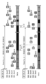
- FIG. 1 is a diagram illustrating an example of the operation of a command scheduler.
- FIG. 2 is a diagram illustrating an example of the operation following FIG. 1.
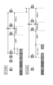
- FIG. 3 is a diagram illustrating an example of the operation of the command scheduler.
- FIG. 4 is a diagram illustrating an example of the operation of the command scheduler.
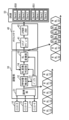
- FIG. 5 is a diagram illustrating a schematic configuration example of an information processing system including a memory control device according to an embodiment of the present disclosure.
- FIG. 6 is a diagram showing the concept of FIFO memory.
- FIG. 7 is a diagram illustrating an example of data stored in the FIFO memory.
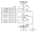
- FIG. 8 is a diagram illustrating an example of the operation of the RW switching detection section.
- FIG. 1 is a diagram illustrating an example of the operation of a command scheduler.
- FIG. 2 is a diagram illustrating an example of the operation following FIG. 1.
- FIG. 3 is a diagram illustrating an example of the operation of the command scheduler.
- FIG. 9 is a diagram showing conditions for determining whether to convert the BL length of a command included in 2BG interleaving.
- FIG. 10 is a diagram illustrating the conditions of FIG. 9.
- FIG. 11 is a diagram illustrating the conditions of FIG. 9.
- FIG. 12 is a diagram illustrating the conditions of FIG. 9.
- FIG. 13 is a diagram illustrating an example of the operation of the BL conversion determination section.
- FIG. 14 is a diagram illustrating an example of the operation of the BL conversion determination section.
- FIG. 15 is a diagram illustrating an example of the operation of the BL conversion determination section.
- FIG. 16 is a diagram illustrating an example of the operation of the BL conversion section.
- FIG. 17 is a diagram illustrating an example of data stored in the FIFO memory.
- FIG. 10 is a diagram illustrating the conditions of FIG. 9.
- FIG. 11 is a diagram illustrating the conditions of FIG. 9.
- FIG. 12 is a diagram illustrating the conditions of FIG. 9.
- FIG. 18 is a diagram illustrating an example of a memory access request string after conversion by the BL conversion unit.
- FIG. 19 is a diagram illustrating an example of data stored in the FIFO memory.
- FIG. 20 is a diagram illustrating an example of a memory access request sequence after conversion by the BL conversion unit.
- FIG. 21 is a diagram illustrating an example of an out-of-order execution procedure.
- FIG. 22 is a diagram illustrating an example of an out-of-order execution procedure.
- FIG. 23 is a diagram illustrating an example of the operation of the command scheduler when an access request sequence that changes from a read request to a write request is input.
- FIG. 24 is a diagram illustrating an example of the operation of the command scheduler when an access request sequence that changes from a write request to a read request is input.
- FIG. 25 is a diagram illustrating a modified example of the schematic configuration of the information processing system of FIG. 5.
- FIG. 26 is a diagram illustrating a modified example of the schematic configuration of the information processing system in FIG. 5.
- FIG. 27 is a diagram showing conditions for determining whether to convert the BL length of a command included in 2BG interleaving.
- FIG. 28 is a diagram illustrating the conditions of FIG. 27.
- FIG. 29 is a diagram showing an example of data stored in the FIFO memory.
- FIG. 30 is a diagram illustrating an example of an access request string after conversion by the BL conversion unit.
- SDRAM synchronous DRAM
- This SDRAM is a DRAM that operates in synchronization with a clock signal, and is often composed of a plurality of banks.
- LPDDR5 and LPDDR5X are DRAM standards defined by JEDEC (Join Electron Device Engineering Council).
- FIGS. 1 and 2 show an example of the operation of the command scheduler when interleaving is performed in two bank groups.
- FIG. 2 shows an example of the operation following FIG. 1.
- the upper rows of FIGS. 1 and 2 show an example of the operation of the command scheduler when the BL length is BL16.
- the lower portions of FIGS. 1 and 2 show an example of the operation of the command scheduler when the BL length is BL32.
- the commands output to the address command lines are divided into bank groups and bank addresses, and the data output to the data lines are divided into bank groups and bank addresses. are represented in different patterns. Note that in the data line, blacked out areas indicate that no data is output.
- ⁇ tRRD Shortest interval between ACT-ACT ⁇ tFAW: Period in which up to four ACTs may exist
- ⁇ tRCD Shortest interval between ACT-READ or ACT-MASKED WRITE
- ⁇ tRCD_W Shortest interval between ACT-WRITE ⁇ nRBTP: READ- burst end-PRE shortest interval tRPpb: PRE-ACT shortest interval tWR: WRTE recovery time
- FIGS. 3 and 4 illustrate an example of the operation of the command scheduler.
- the upper rows of FIGS. 3 and 4 show an example of the operation of the command scheduler when the BL length is BL16.
- the lower portions of FIGS. 3 and 4 show an example of the operation of the command scheduler when the BL length is BL32.
- the data line of DRAM is shared for reading and writing. Therefore, a penalty time is required when switching from read to write or from write to read.
- BL/n_min of BL16 is 2, while BL/n_min of BL32 is 6. Therefore, as shown in FIGS. 3 and 4, it can be seen that the timing at which a write command is issued may be earlier in BL16 than in BL32, depending on the usage status of the data line. Therefore, it can be seen that in the latest generation standards, BL16 is sometimes more efficient in accessing the DRAM than BL32.
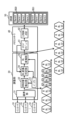
- FIG. 5 shows an example of a schematic configuration of an information processing system including a memory control device according to an embodiment of the present disclosure.
- the information processing system includes, for example, a plurality of initiators 10, an adjustment section 30, a memory controller 40, and a DRAM 50, as shown in FIG.
- the DRAM 50 is a DRAM compliant with LPDDR5 or LPDDR5X.
- two bank groups BG0 and GB1 are defined in the DRAM 50.
- four banks Bank0, Bank1, Bank2, and Bank3 are defined in each bank group BG0, GB1.
- the respective numbers of bank groups and banks in the DRAM 50 are not limited to the above example.
- LPDDR5 or LPDDR5X it is possible to dynamically change the drive frequency. Furthermore, LPDDR5 or LPDDR5X has a plurality of bank modes, which are ways to use the bank configuration, and the specification that the bank mode changes depending on the drive frequency has been standardized.
- the 16B (Bank) mode is used at a low drive frequency
- the BG (Bank Group) mode is used at a high drive frequency.
- the BG mode in the case of data transfer by BL32, data transfer in response to a command is performed with a period of 16 BL (1nCK).
- Such a transfer penalty on the data line is a regulation specific to the BG mode. However, since transfer data of another bank group can be entered during this transfer penalty period, it is possible to issue transfer data continuously on the data line.
- the plurality of initiators 10 write data to or read data from the DRAM 50 via the adjustment unit 30 and the memory controller 40.
- Each initiator 10 is, for example, a central processing unit (CPU) or a functional block.
- Each initiator 10 issues a memory access request for writing or reading data to or from the DRAM 50 and outputs it to the adjustment unit 30.
- This memory access request includes, for example, a logical address in a virtual storage area given to each initiator 10, a BL length that is the length of data to be accessed, identification information for identifying the initiator 10, and a transfer direction. included. The transfer direction here indicates whether it is a write request for writing data or a read request for reading data.
- Each initiator 10 outputs write data to be written to the DRAM 50 to the adjustment unit 30 in accordance with a data output instruction from the adjustment unit 30.
- Each initiator 10 communicates with the adjustment unit 30 using, for example, a protocol defined by AMBA (Advanced Microcontroller Bus Architecture) (for example, AXI (Advanced eXtensible Interface) protocol).
- AMBA Advanced Microcontroller Bus Architecture
- AXI Advanced eXtensible Interface
- the adjustment section 30 includes, for example, as shown in FIG. 5, an arbitration section 31, an RW switching detection section 32, a buffer 33, a BL conversion determination section 34, and a BL conversion section 35.
- the arbitration unit 31 converts the logical address included in the memory access request output from each initiator 10 into a physical address corresponding to the DRAM 50.
- the physical address referred to herein is an address that indicates a bank, row, and column that constitute the DRAM 50, and refers to a bank address, a row address, and a column address. By converting a logical address into a physical address in this way, the bank address, row address, and column address in the DRAM 50 are indicated in the converted memory access request.
- the arbitration unit 31 further performs arbitration based on the physical addresses indicated in the plurality of memory access requests obtained from the plurality of initiators 10. For example, when receiving memory access requests from each initiator 10 at the same time, the arbitration unit 31 suppresses output of a memory access request having the same bank address as the memory access request output to the RW switching detection unit 32 immediately before. . That is, when the arbitration unit 31 receives a plurality of memory access requests, it outputs to the RW switching detection unit 32 a memory access request that has a different bank address from the memory access request output to the RW switching detection unit 32 immediately before. In this way, the arbitration unit 31 uses the interleaving method to adjust the order in which multiple memory access requests are output to the RW switching detection unit 32.
- the arbitration unit 31 adjusts the output order of the plurality of memory access requests to the RW switching detection unit 32 using an interleaving method for each bank group. At this time, the arbitration unit 31 adds the bank group identifier to the memory access request.
- the arbitration unit 31 sends a write request corresponding to the memory access request to the initiator 10 identified by the identification information indicated in the memory access request. Instructs to output data.
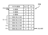
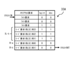
- the buffer 33 includes, for example, a FIFO (First-In First-Out) memory 33A as shown in FIG.
- FIFO First-In First-Out
- a FIFO memory 33A a plurality of memory access requests are stored in the order of storage, and when a new memory access request is stored in the FIFO memory 33A, the memory access request with the oldest storage order is output from the FIFO memory 33A.
- bank group information bgint and division necessity information dev are associated with each stored memory access request. Every time a new memory access request is stored, the FIFO memory 33A outputs the memory access request with the oldest storage order in the FIFO memory 33A to the BL converter 35 along with bank group information bgint and division necessity information dev.
- the bank group information bgint is a flag for determining whether among the plurality of memory access requests stored in the FIFO memory 33A, it is a BG interleaved memory access request placed immediately before switching between read and write. For example, when the bank group information bgint is "1", it means that it is a memory access request for BG interleave arranged immediately before switching between read and write. Further, for example, when the bank group information bgint is "0", it means that the request is not a memory access request for BG interleaving arranged immediately before switching between read and write.
- the division necessity information dev is a flag for determining whether or not to convert the BL length of the BG interleave memory access request included in the FIFO memory 33A from BL32 to BL16. For example, when the division necessity information dev is "1", it means that the BL length of the memory access request needs to be converted from BL32 to BL16. Further, for example, when the division necessity information dev is "0", it means that there is no need to convert the BL length of the memory access request from BL32 to BL16.
- the RW switching detection unit 32 detects a switch from read BG interleave (read request) to a write request or a switch from write BG interleave (write request) to a read request in a plurality of memory access requests stored in the buffer 33. . For example, suppose that a plurality of memory access requests as shown in FIG. 7 are stored in the FIFO memory 33A. At this time, the RW switching detection unit 32 detects the difference between the read request and the write request in the memory access request (read request) whose storage order is the fifth oldest and the memory access request (write request) whose storage order is the sixth oldest. Detect switching.
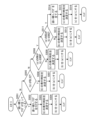
- FIG. 8 shows an example of the procedure for detecting the above-mentioned switching in the RW switching detection section 32.
- the RW switching detection unit 32 sets the parameter i indicating the storage order to 0 (step S101).
- the RW switching detection unit 32 determines whether the parameter i is smaller than the latest storage order N-1 (step S102). As a result, if i ⁇ N-1 is satisfied (step S102; Y), the RW switching detection unit 32 compares the memory access request with the storage order i and the memory access request with the storage order i+1, It is determined whether both are read requests or write requests (step S103).
- step S103; Y the RW switching detection unit 32 adds 1 to the parameter i (step S104), and returns to step S102. If neither is a read request or a write request (step S103; N), the RW switching detection unit 32 changes the read request to the write request in the memory access request whose storage order is i and the memory access request whose storage order is i+1. , or from a write request to a read request. Then, the RW switching detection unit 32 writes "1" to the bank group information bgint corresponding to the memory access request with the storage order i, and proceeds to determine whether BL conversion is necessary (step S105).
- the RW switching detection unit 32 outputs the parameter i to the BL conversion determination unit 34 as information about the switching (RW switching information). Note that in step S102, if i ⁇ N-1 is not satisfied (step S102; N), this process is performed assuming that there is no switching from a read request to a write request or from a write request to a read request. finish.
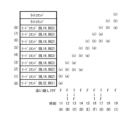
- the BL conversion determination unit 34 and the BL conversion unit 35 determine the number of memory access requests for the 2BG interleave IL-a (read BG group interleave or write BG interleave) immediately before the switching, and the memory access request immediately before the 2BG interleave IL-a.
- the BL length of the memory access request included in the 2BG interleaved IL-a is converted based on the timing information of the command Cmd-a (first command) corresponding to Ra. Note that "2BG interleaving" refers to interleaving into two bank groups.
- the BL conversion determining unit 34 and the BL converting unit 35 determine whether to convert the BL length of the memory access request included in the 2BG interleaved IL-a based on the conditions shown in FIG. .
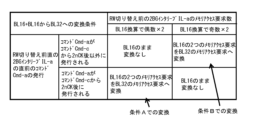
- FIG. 9 shows the conditions for determining whether to convert the BL length of the memory access request included in the 2BG interleaved IL-a.
- FIG. 9 shows conditions for converting the BL length of a memory access request included in 2BG interleaved IL-a from BL32 to BL16.
- the BL conversion determination unit 34 and the BL conversion unit 35 convert the BL length of the memory access request included in the 2BG interleaved IL-a from BL32 to BL16 when either of the following two conditions is satisfied.
- command Cmd-b included in condition A below is a command corresponding to the memory access request R-b immediately preceding the memory access request R-a.
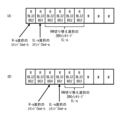
- FIGS. 10(A) and 10(B) are diagrams explaining the 2BG interleave IL-a, command Cmd-a, and command Cmd-b.
- FIG. 10A a case is illustrated in which the 2BG interleaving IL-a is configured to interleave two bank groups BG2 and BG3 with four read commands of BL32.
- FIG. 10B a case is illustrated in which the 2BG interleave IL-a is configured to interleave two bank groups BG2 and BG3 with two read commands of BL32.
- command Cmd-a is a read command of BL32 for bank group BG1
- command Cmd-b is a read command of BL32 for bank group BG2.
- command Cmd-a is a read command for BL32 for bank group BG1
- command Cmd-b is a read command for BL32 for bank group BG0.
- FIG. 11(A) shows an example of the timing at which each command is output to the command access line CA when a plurality of commands are arranged in the order shown in FIG. 10(A).
- FIG. 11B shows an example of the timing at which each transfer data is output to the data line DQ when each command is output to the command access line CA at the timing shown in FIG. 11A.
- command Cmd-a is issued 2nCK after command Cmd-b is issued.
- FIG. 12(A) shows an example of the timing at which each command is output to the command access line CA when a plurality of commands are arranged in the order shown in FIG. 10(A).
- FIG. 12B shows an example of the timing at which each transfer data is output to the data line DQ when each command is output to the command access line CA at the timing shown in FIG. 12A.
- command Cmd-a is issued 6nCK after command Cmd-b is issued.
- command Cmd-a When command Cmd-a is issued 2nCK after command Cmd-b is issued, the data line DQ is You can see that it is filled in without any gaps. However, if command Cmd-a is issued 6nCK after command Cmd-b is issued, the data transfer for command Cmd-a is performed with a gap of BL16 minutes (1nCK). The gap is not filled with the transfer data corresponding to command Cmd-b and remains empty. Conditions under which such a gap occurs corresponds to condition A.
- FIG. 13 shows an example of a procedure for determining whether or not BL conversion is necessary in the BL conversion determination unit 34.
- FIG. 13 illustrates the FIFO memory 33A in which all flags have been initialized.
- the BL conversion determination unit 34 first copies the parameter i acquired from the RW switching detection unit 32 to the parameter j (step S201). Next, the BL conversion determination unit 34 determines whether the parameter j is 0 or more (step S202). If the parameter j is 0 or more (step S202; Y), the BL conversion determination unit 34 accesses the memory access request whose storage order is j stored in the FIFO memory 33A, and accesses the memory access request whose storage order is j. Read the BG identifier included in the access request.
- the BL conversion determination unit 34 records in the internal memory the identifiers of BGs and their number (the number of BGs) included in the memory access requests accessed from the start of execution of step S201 until now (step S203). .
- the BL conversion determination unit 34 further records in the internal memory the number of memory access requests that have been accessed since the start of execution of step S201. If the parameter j is a negative value (step S202; N), the process moves to a determination of whether or not division information is generated (step S204).
- the BL conversion determination unit 34 determines whether the number of BGs recorded in the internal memory is greater than 2 (step S205). If the number of BGs recorded in the internal memory is greater than 2 (step S205; Y), the process moves to a division necessity information generation determination (step S204). If the number of BGs recorded in the internal memory is 2 or less (step S205; N), it is determined whether or not the two most recently recorded BG identifiers are equal to each other among the BG identifiers recorded in the internal memory. (Step S206).
- step S206; Y If the identifiers of the two most recently recorded BGs are equal to each other (step S206; Y), the BL conversion determination unit 34 determines that the most recently accessed memory access request is not a valid request, and ends this process. do. If the identifiers of the two most recently recorded BGs are different from each other (step S206; N), the BL conversion determination unit 34 determines that the most recently accessed memory access request is a valid request. Then, the BL conversion determination unit 34 writes "1" to the bank group information bgint corresponding to the memory access request whose storage order is j, which is stored in the FIFO memory 33A. The BL conversion determination unit 34 further subtracts 1 from the parameter j (step S207), and returns to step S202.
- FIG. 14 shows an example of a determination procedure for generating division necessity information (step S204) in the BL conversion determination unit 34.
- FIG. 14 shows an example of the FIFO memory 33A in which the flag after the processing shown in FIG. 13 has been written.
- the BL conversion determination unit 34 determines whether the parameter j is 0 (step S301). If the parameter j is 0 (step S301; Y), the BL conversion determination unit 34 proceeds to create division necessity information (step S302). If the parameter j is not 0 (step S301; N), the BL conversion determination unit 34 ends the determination of generation of division necessity information.
- FIG. 15 shows an example of a procedure for creating division necessity information in the BL conversion determination unit 34.
- FIG. 15 shows an example of the FIFO memory 33A in which the flag after the processing shown in FIG. 15 has been written.
- the BL conversion determination unit 34 determines whether the number of memory access requests recorded in the internal memory is an even number ⁇ 2 (step S401).
- the above-mentioned "number of memory access requests recorded in internal memory” is the number of memory access requests of the BG interleave IL-a (the number of memory access requests when converted to BL16 equivalent).
- the BL conversion determination unit 34 uses the command Based on the issue timing information obtained from the scheduler 41, it is determined whether command Cmd-a is shifted by 2nCK from command Cmd-b (step S402).
- the issuance timing (issuance time) of command Cmd-b and the issuance timing (issuance time) of command Cmd-a are obtained from the issuance timing information obtained from the command scheduler 41.
- the BL conversion determination unit 34 can determine whether command Cmd-a is shifted by 2nCK from command Cmd-b from these issuing times.
- the BL conversion determination unit 34 responds to the memory access request of the BG interleave IL-a in the FIFO memory 33A. "1" is written in the division necessity information dev (step S403).
- step S401 if the number of memory access requests for BG interleaved IL-a (the number of memory access requests when converted to BL16 equivalent) is an odd number x 2 (step S401; N), the BL conversion determination unit 34 determines whether command Cmd-a is shifted by 2nCK from command Cmd-b based on the issuance timing information obtained from command scheduler 41 (step S404). Specifically, it is assumed that the issuance timing (issuance time) of command Cmd-b and the issuance timing (issuance time) of command Cmd-a are obtained from the issuance timing information obtained from the command scheduler 41. At this time, the BL conversion determination unit 34 can determine whether command Cmd-a is shifted by 2nCK from command Cmd-b from these issuing times.
- step S404 if the command Cmd-a is shifted by 2nCK from the command Cmd-b (step S404; Y), the BL conversion determination unit 34 responds to the memory access request of the BG interleave IL-a in the FIFO memory 33A. "1" is written in the division necessity information dev (step S403).
- step S404 if memory access request R-a is not shifted by 2nCK from memory access request R-b (step S404; N), or in step S402, memory access request R-a is not shifted by 2nCK from memory access request R-b.
- the BL conversion determination unit 34 writes "0" to the division necessity information dev corresponding to the memory access request of the BG interleave IL-a in the FIFO memory 33A (step S405). ).
- FIG. 16 shows an example of a BL conversion procedure in the BL conversion unit 35.
- the FIFO memory 33A outputs the memory access request with the oldest storage order in the FIFO memory 33A to the BL conversion unit 35 together with the division necessity information dev.
- the BL conversion unit 35 determines whether the division necessity information dev is "1" (step S501). As a result, if the division necessity information dev is "1" (step S501; Y), the BL conversion unit 35 converts the BL length of the memory access request from BL32 to BL16 (step S502).
- the BL conversion unit 35 divides the memory access request of BL32 into two memory access requests of BL16. If the division necessity information dev is "0" (step S501; N), the BL conversion unit 35 does not change the BL length of the memory access request as BL32 (step S503).
- FIG. 17 shows an example of the FIFO memory 33A after the flag writing process is performed when condition A is satisfied.
- the output from the BL conversion unit 35 when a plurality of memory access requests are sequentially input to the FIFO memory 33A shown in FIG. 17 will be described.
- the memory access request with the oldest storage order in the FIFO memory 33A (read request at the beginning of 2BG interleaved IL-a (BL32, BG2)) and division necessity information dev are It is output to the BL conversion section 35.
- the memory access request with the oldest storage order in the FIFO memory 33A (second read request (BL32, BG3) of 2BG interleaved IL-a) and division necessity information dev is output to the BL conversion section 35.
- the BL conversion unit 35 thereafter outputs a memory access request to the memory controller 40 in the same manner as described above.
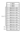
- a memory access request string as shown in FIG. 18 is input to the memory controller 40.
- a plurality of memory access requests input to the memory controller 40 are arranged in order from the bottom.
- FIG. 19 shows an example of the FIFO memory 33A after the flag writing process is performed when condition B is satisfied. Below, the output from the BL converter 35 when a plurality of commands are sequentially input to the FIFO memory 33A shown in FIG. 19 will be described.
- the memory access request with the oldest storage order in the FIFO memory 33A (read request at the beginning of 2BG interleaved IL-a (BL32, BG2)) and division necessity information dev are It is output to the BL conversion section 35.
- the memory access request with the oldest storage order in the FIFO memory 33A (second read request (BL32, BG3) of 2BG interleaved IL-a) and division necessity information dev is output to the BL conversion section 35.
- the BL conversion unit 35 thereafter outputs a memory access request to the memory controller 40 in the same manner as described above.
- a memory access request string as shown in FIG. 20 is input to the memory controller 40.
- a plurality of memory access requests input to the memory controller 40 are arranged in order from the bottom.
- the memory controller 40 includes a command scheduler 41 and an LPDDR-PHY (hereinafter simply referred to as "physical layer") 42.
- the command scheduler 41 issues commands to the DRAM 50 based on the memory access request input from the adjustment unit 30. At this time, the command scheduler 41 generates issue timing information of the command to be issued, and outputs the command to the physical layer 42 according to the generated issue timing information. The command scheduler 41 outputs the generated issue timing information to the BL conversion determination unit 34.
- the command scheduler 41 issues commands to a plurality of bank groups in the DRAM 50 using a bank group interleaving method to access the bank groups in parallel.
- the memory controller 40 outputs the write data stored in the internal buffer to the DRAM 50 in synchronization with the command issuance.
- the memory controller 40 reads read data from the DRAM 50 and stores it in an internal buffer in synchronization with the command issuance.
- the physical layer 42 outputs commands supplied in synchronization with the operating clock of the memory controller 40 and write data stored in an internal buffer based on the memory clock of the DRAM 50. Further, the physical layer 42 stores data read out in synchronization with the memory clock in the DRAM 50 in an internal buffer in synchronization with the operation clock of the memory controller 40.
- the command scheduler 41 has a function (out-of-order execution function) of rearranging the access order in order to improve the efficiency of memory access.
- the out-of-order execution function will be explained below.
- FIG. 21 shows an example of an out-of-order execution procedure.
- the command scheduler 41 determines whether the overtaking flag is set (step S501). As a result, if the overtaking flag is set (step S501; Y), the command scheduler 41 clears the overtaking flag (step S502). At this time, the command scheduler 41 determines the issue time of the command corresponding to (b), and sets the command corresponding to (b) as the command corresponding to (a) (steps S502, S503).
- step S501; N the command scheduler 41 determines whether the BL length of the command corresponding to (b) is BL32 (step S505). As a result, if the BL length of the command corresponding to (b) is BL32 (step S505; Y), the command scheduler 41 determines the issue time of the command corresponding to (b), and The corresponding command is set as the command corresponding to (a) (steps S506, S507).
- the command scheduler 41 determines whether the command corresponding to (a) and the command corresponding to (b) are mutually read commands or It is determined whether it is a write command (step S508). As a result, if the command corresponding to (a) and the command corresponding to (b) are not read commands or write commands (step S508; N), the command scheduler 41 commands the command corresponding to (b). The issuance time of is determined, and the command corresponding to (b) is set as the command corresponding to (a) (steps S509, S510).
- the command scheduler 41 determines that the BG of the command corresponding to (a) is It is determined whether it is equal to the BG of the command corresponding to (b) (step S511). As a result, if the BG of the command corresponding to (a) is different from the BG of the command corresponding to (b) (step S511; N), the command scheduler 41 issues the command corresponding to (b). The time is determined, and the command corresponding to (b) is made the command corresponding to (a) (steps S512, S513).
- step S511; Y If the BG of the command corresponding to (a) is equal to the BG of the command corresponding to (b) (step S511; Y), the command scheduler 41 sets an overtaking flag (step S514). Subsequently, the command scheduler 41 determines the issue time of the command corresponding to (c), and sets the command corresponding to (c) as the command corresponding to (a) (steps S515, S516).
- FIG. 22 shows an example of a command string generated by the command scheduler 41. Each time in FIG. 22 is an issuance time determined for the command corresponding to (b), and the command corresponding to (c) is the next oldest command after the command corresponding to (b).
- the command scheduler 41 has no overtaking flag set, the BL length of the command corresponding to (b) is BL16, and the command corresponding to (a) and ( Assume that the commands corresponding to b) are both read commands, and the BG of the command corresponding to (a) is different from the BG of the command corresponding to (b) (steps S501; N, 505; N , S508; Y, S511; N).
- the command scheduler 41 sets the issue time of the command corresponding to (b) to t1 (step S512).
- the command scheduler 41 outputs the command corresponding to (a) to the physical layer 42, and changes the command corresponding to (b) to the command corresponding to (a) (step S513).
- the command scheduler 41 determines that the overtaking flag is not set, the BL length of the command corresponding to (b) is BL16, and the BL length of the command corresponding to (a) is Assume that the command and the command corresponding to (b) are both read commands, and the BG of the command corresponding to (a) is equal to the BG of the command corresponding to (b) (step S501; N , 505; N, S508; Y, S511; Y). At this time, the command scheduler 41 sets an overtaking flag and sets the issuing time of the command corresponding to (c) to t2 (steps S514, S515). Furthermore, the command scheduler 41 outputs the command corresponding to (a) to the physical layer 42, and changes the command corresponding to (c) to the command corresponding to (a) (step S516).
- step S501 if the overtaking flag is set (step S501; Y), the command scheduler 41 clears the overtaking flag (step S502). At this time, the command scheduler 41 sets the issue time of the command corresponding to (b) to t3 (step S503). Furthermore, the command scheduler 41 outputs the command corresponding to (a) to the physical layer 42, and changes the command corresponding to (b) to the command corresponding to (a) (step S504).
- the command scheduler 41 determines that the overtaking flag is not set, the BL length of the command corresponding to (b) is BL16, and the command corresponding to (a) is not set. Assume that the command and the command corresponding to (b) are both read commands, and the BG of the command corresponding to (a) is different from the BG of the command corresponding to (b) (step S501; N, 505; N, S508; Y, S511; N). At this time, the command scheduler 41 sets the issue time of the command corresponding to (b) to t4 (step S512). Furthermore, the command scheduler 41 outputs the command corresponding to (a) to the physical layer 42, and changes the command corresponding to (b) to the command corresponding to (a) (step S513).
- the command scheduler 41 determines that the overtaking flag is not set, the BL length of the command corresponding to (b) is BL16, and the command corresponding to (a) is Assume that the command and the command corresponding to (b) are both read commands, and the BG of the command corresponding to (a) is different from the BG of the command corresponding to (b) (step S501; N, 505; N, S508; Y, S511; N). At this time, the command scheduler 41 sets the issue time of the command corresponding to (b) to t5 (step S512). Furthermore, the command scheduler 41 outputs the command corresponding to (a) to the physical layer 42, and changes the command corresponding to (b) to the command corresponding to (a) (step S513).
- the command scheduler 41 determines that the overtaking flag is not set, the BL length of the command corresponding to (b) is BL16, and the command corresponding to (a) is not set. Assume that the command and the command corresponding to (b) are both read commands, and the BG of the command corresponding to (a) is equal to the BG of the command corresponding to (b) (step S501; N , 505; N, S508; Y, S511; Y). At this time, the command scheduler 41 sets an overtaking flag and sets the issuing time of the command corresponding to (c) to t6 (steps S514, S515). Furthermore, the command scheduler 41 outputs the command corresponding to (a) to the physical layer 42, and changes the command corresponding to (c) to the command corresponding to (a) (step S516).
- the command scheduler 41 assumes that the overtaking flag is set, as shown in FIG. 22(G) (step S501; Y). At this time, the command scheduler 41 clears the overtaking flag and sets the issuing time of the command corresponding to (b) to t7 (steps S502, S503). Furthermore, the command scheduler 41 outputs the command corresponding to (a) to the physical layer 42, and changes the command corresponding to (b) to the command corresponding to (a) (step S504).
- the command scheduler 41 determines that the overtaking flag is not set, the BL length of the command corresponding to (b) is BL16, and the command corresponding to (a) is not set. Assume that the command and the command corresponding to (b) are both read commands, and the BG of the command corresponding to (a) is different from the BG of the command corresponding to (b) (step S501; N, 505; N, S508; Y, S511; N). At this time, the command scheduler 41 sets the issue time of the command corresponding to (b) to t8 (step S512). Furthermore, the command scheduler 41 outputs the command corresponding to (a) to the physical layer 42, and changes the command corresponding to (b) to the command corresponding to (a) (step S513).
- the command scheduler 41 assumes that the overtaking flag is not set and the BL length of the command corresponding to FIG. 22(b) is BL32 (step S501; , 505; Y). At this time, the command scheduler 41 sets the issue time of the command corresponding to (b) to t9 (step S506). Furthermore, the command scheduler 41 outputs the command corresponding to (a) to the physical layer 42, and changes the command corresponding to (b) to the command corresponding to (a) (step S507).
- the command scheduler 41 executes out-of-order.
- FIG. 23 shows an example of the operation of the command scheduler 41 when a command sequence changing from a read command to a write command is input.
- the upper part of FIG. 23 shows an example of the operation of the command scheduler 41 when the BL length is BL32.
- the lower part of FIG. 23 shows an example of the operation of converting the BL length of a plurality of read commands (BL32, BG3) of a specific BG interleave from BL32 to BL16 in the operation of the command scheduler 41 shown in the upper part of FIG. It is represented.
- a specific BG interleave refers to a BG interleave that is composed of a plurality of commands whose division necessity information dev is "1".
- the commands output to the address command line are shown divided by bank group and bank address, and the data output to the data line appears to be different for each bank group and bank address. It is expressed as. Note that in the data line, blacked out areas indicate that no data is output.
- FIG. 24 shows an example of the operation of the command scheduler 41 when a command sequence changing from a write command to a read command is input.
- the upper part of FIG. 24 shows an example of the operation of the command scheduler 41 when the BL length is BL32.
- the lower part of FIG. 24 shows an example of the operation of converting the BL length of multiple read commands (BL32, BG3) of a specific BG interleave from BL32 to BL16 in the operation of the command scheduler 41 shown in the upper part of FIG. It is represented.
- a specific BG interleave refers to a BG interleave that is composed of a plurality of commands whose division necessity information dev is "1".
- the commands output to the address command line are shown divided by bank group and bank address, and the data output to the data line appears to be different for each bank group and bank address. It is expressed as. Note that in the data line, blacked out areas indicate that no data is output.
- read BG interleaving is performed based on the number of memory access requests for read BG interleaving or write BG interleaving and the timing information of the command corresponding to the memory access request immediately before read bank group interleaving or write bank group interleaving.
- the BL length of the memory access request included in the write BG interleave is converted. This makes it possible to select the BL length in consideration of the efficiency of access to the DRAM 50. As a result, access to the DRAM 50 can be executed more efficiently in a DRAM standard that has a BG and supports multiple BL lengths, such as LPDDR5 or LPDDR5X.
- the BL length of the memory access request included in the read BG interleave or the write BG interleave is converted from BL32 to BL16. This makes it possible to select the BL length in consideration of the efficiency of access to the DRAM 50. As a result, access to the DRAM 50 can be executed more efficiently in a DRAM standard that has a BG and supports multiple BL lengths, such as LPDDR5 or LPDDR5X.
- the present embodiment it is determined whether or not to convert the BL lengths of multiple memory access requests to which flags have been added based on the issue timing information obtained from the command scheduler 41, and the flags are set according to the determination result. It is written into the FIFO memory 33A of the buffer 33 as division necessity information dev. This makes it possible to select the BL length in consideration of the efficiency of access to the DRAM 50 using the FIFO memory 33A. As a result, access to the DRAM 50 can be executed more efficiently in a DRAM standard that has a BG and supports multiple BL lengths, such as LPDDR5 or LPDDR5X.
- a memory controller 60 may be provided in place of the adjustment section 30 and the memory controller 40.
- the memory controller 60 has a command scheduler 43 and a physical layer 42.
- the command scheduler 43 includes, for example, a buffer 43a, an RW switching detection section 32, a BL conversion section 35, a BL conversion determination section 34, and a command issuing section 43b.
- the buffer 43a includes, for example, a FIFO memory 33A. Each time the buffer 43a receives a memory access request from the arbitration unit 31, the buffer 43a stores the received memory access request in the FIFO memory 33A.
- the BL conversion unit 35 outputs the memory access request output from the FIFO memory 33A of the buffer 43a to the command issuing unit 43b.
- the command issuing unit 43b issues a command to the DRAM 50 based on the memory access request input from the BL converting unit 35. For example, the command issuing unit 43b issues commands to a plurality of bank groups in the DRAM 50 using a bank group interleaving method for accessing in parallel. The command issuing unit 43b outputs the write data stored in the internal buffer to the DRAM 50 in synchronization with issuing the command. The command issuing unit 43b reads read data from the DRAM 50 and stores it in an internal buffer in synchronization with command issuing.
- the function of the adjustment section 30 is built into the memory controller 60.
- the command buffer within the memory controller 60 can be used as the buffer 43a.
- the command issuing unit 43b may output information about the usage status of the DQ pins managed within the memory controller 60 to the BL conversion determining unit 34.
- the BL conversion determination unit 34 determines whether or not a vacant space as shown in FIG. whether or not). As a result, if it is determined that a vacant space as shown in FIG. 12(B) occurs in the DQ pin (that is, the above-mentioned condition A is satisfied), the BL length of the command included in the 2BG interleaved IL-a is Convert from BL32 to BL16. Even in this case, it is possible to select the BL length in consideration of the efficiency of access to the DRAM 50. As a result, access to the DRAM 50 can be executed more efficiently in the latest generation DRAM standards such as LPDDR5 or LPDDR5X.
- the BL length included in the memory access request input from each initiator 10 was always BL32.
- the BL length included in a part of the memory access request input from each initiator 10 may be, for example, BL16 as shown in FIG. 26.
- FIG. 27 shows the conditions for determining whether to convert the BL length of the command included in the 2BG interleaved IL-a.
- FIG. 27 shows conditions for converting the BL length of a command included in 2BG interleaved IL-a from BL16 to BL32.
- the BL conversion determination unit 34 and the BL conversion unit 35 convert the BL length of the command included in the 2BG interleaved IL-a from BL16 to BL32 when neither of the following two conditions is satisfied.
- FIGS. 28(A) and 28(B) are diagrams for explaining 2BG interleave IL-a, command Cmd-a, and command Cmd-b.
- FIG. 28A illustrates a case where the 2BG interleave IL-a is configured to interleave two bank groups BG2 and BG3 with eight read requests of BL16.
- FIG. 29B a case is illustrated in which the 2BG interleave IL-a is configured to interleave two bank groups BG2 and BG3 with four read commands of BL16.
- the command Cmd-a immediately before the 2BG interleave IL-a is a read command of BL32 for bank group BG1
- the command Cmd-b immediately before command Cmd-a is the command for bank group BG2.
- the command Cmd-a immediately before the 2BG interleave IL-a is a read command of BL32 for bank group BG1
- the command Cmd-b immediately before the command Cmd-a is the command for the bank group BG1. This is a read command for BL32 for group BG0.
- the BL length of the memory access request included in the read BG interleave or the write BG interleave is converted from BL16 to BL32. This makes it possible to select the BL length in consideration of the efficiency of access to the DRAM 50. As a result, access to the DRAM 50 can be executed more efficiently in a DRAM standard that has a BG and supports multiple BL lengths, such as LPDDR5 or LPDDR5X.
- the command scheduler 41 may interleave three bank groups.
- the BL conversion determination unit 34 and the BL conversion unit 35 determine the number of memory access requests for 3BG interleave IL-b (read BG group interleave or write BG interleave) immediately before the read/write switching, and the number of memory access requests for 3BG interleave IL-b (read BG group interleave or write BG interleave)
- the BL length of the memory access request included in the 3BG interleave IL-b is converted based on the timing information of the command Cmd-a (first command) corresponding to the immediately preceding memory access request Ra.
- 3BG interleaving refers to interleaving into three bank groups.
- the BL conversion determination unit 34 and the BL conversion unit 35 determine whether to convert the BL length of the memory access request included in the 3BG interleaved IL-b based on condition A or condition B described below. may be judged.
- the buffer 33 stores, for example, the FIFO memory 33A shown in FIG.
- FIG. 29 shows an example of the FIFO memory 33A in which flags are written after flag writing processing is performed when condition A is satisfied.
- the output from the BL conversion unit 35 when a plurality of memory access requests are sequentially input to the FIFO memory 33A shown in FIG. 29 will be described.
- the memory access request with the oldest storage order in the FIFO memory 33A (read request at the beginning of 3BG interleaved IL-b (BL32, BG1)) and division necessity information dev are It is output to the BL conversion section 35.
- the memory access request with the oldest storage order in the FIFO memory 33A (second read request (BL32, BG3) of 3BG interleaved IL-b) and division necessity information dev is output to the BL conversion section 35.
- the BL conversion unit 35 outputs commands to the memory controller 40 in the same manner as described above.
- a memory access request string as shown in FIG. 30 is input to the memory controller 40.
- a plurality of memory access requests input to the memory controller 40 are arranged in order from the bottom.
- the BL length of the memory access request included in the 3BG interleaved IL-b is converted. Even in this case, it is possible to select the BL length in consideration of the efficiency of access to the DRAM 50. As a result, access to the DRAM 50 can be executed more efficiently in a DRAM standard that has a BG and supports multiple BL lengths, such as LPDDR5 or LPDDR5X.
- the command scheduler 41 may interleave M bank groups.
- the BL conversion determination unit 34 and the BL conversion unit 35 determine the number of memory access requests for MBG interleaved IL-b (M ⁇ 4) immediately before the read/write switching and the memory access request immediately before the MBG interleaved IL-b.
- the BL length of the memory access request included in the MBG interleave IL-b may be converted based on the timing information of the command Cmd-a (first command) corresponding to the request Ra.
- “MBG interleaving” refers to interleaving into M bank groups.
- the BL conversion determination unit 34 and the BL conversion unit 35 determine whether or not to convert the BL length of the memory access request included in the 3BG interleaved IL-b based on condition A or condition B described below. may be judged.
- the present disclosure can take the following configuration.
- a detection unit that detects switching between read bank group interleave and write request or switch between write bank group interleave and read request in a plurality of memory access requests related to received memory access; Based on the number of memory access requests for the read bank group interleave or the write bank group interleave, and the timing information of the first command corresponding to the memory access request immediately before the read bank group interleave or the write bank group interleave, A conversion unit that converts a BL length of a memory access request included in read bank group interleaving or the write bank group interleaving.
- the conversion unit converts the BL length of the memory access request included in the read bank group interleave or the write bank group interleave from BL32 to BL16 when either of the following two conditions is satisfied.
- memory controller ⁇ Condition A
- the number of memory access requests of the read bank group interleave or the write bank group interleave when converted to BL16 equivalent is an even number x 2
- the first command is a second command immediately before the first command. Issued at a timing other than 2nCK after
- the number of memory access requests of the read bank group interleave or the write bank group interleave when converted to BL16 equivalent is an odd number x 2, and the first command is issued at a timing 2nCK after the second command.
- the number of memory access requests of the read bank group interleave or the write bank group interleave when converted to BL16 equivalent is an odd number x 2, and the first command is issued at a timing 2nCK after the second command.
- a storage unit that stores the plurality of memory access requests, bank group information and division necessity information associated with each of the commands; Among the plurality of memory access requests, it is determined whether or not there is a memory access request that corresponds to the read bank group interleave or the write bank group interleave, and a flag according to the determination result is set as the bank group information.
- the memory control device further comprising: a determination unit that writes to the storage unit.
- the determination unit determines whether or not to convert the BL lengths of the plurality of memory access requests to which the flag is attached, based on the timing information, and sets the flag according to the determination result as the division necessity information.
- the memory control device according to (4), wherein the memory control device writes to the storage unit.
- the number of memory access requests for read bank group interleaving or write bank group interleaving and the timing of a command corresponding to a memory access request immediately before read bank group interleaving or write bank group interleaving are provided. Based on this information, the BL length of the memory access request included in the read bank group interleave or the write bank group interleave is converted. This makes it possible to select the BL length in consideration of the efficiency of access to the DRAM. As a result, access to DRAM can be executed more efficiently in a DRAM standard that has a BG and supports multiple BL lengths, such as LPDDR5 or LPDDR5X. Note that the effects of the present disclosure are not necessarily limited to the effects described herein, and may be any effects described in this specification.
Landscapes
- Engineering & Computer Science (AREA)
- Microelectronics & Electronic Packaging (AREA)
- Computer Hardware Design (AREA)
- Theoretical Computer Science (AREA)
- Physics & Mathematics (AREA)
- General Engineering & Computer Science (AREA)
- General Physics & Mathematics (AREA)
- Databases & Information Systems (AREA)
- Dram (AREA)
- Memory System (AREA)
- Information Retrieval, Db Structures And Fs Structures Therefor (AREA)
Abstract
Description
従来、メモリシステムとして、価格、バス帯域および容量の点において有利である同期DRAM(SDRAM:Synchronous Dynamic Random Access Memory)が広く用いられている。このSDRAMは、クロック信号に同期して動作するDRAMであり、多くの場合、複数のバンクにより構成される。
・ACT:Activeコマンド
・READ16:BL16のリードコマンド
・READ32:BL32のリードコマンド
・PRE:Prechargeコマンド
・コマンドクロック=800MHz
・tRRD=3nCK
・tFAW=15ns
・tRCD=15nCK
・tRCD_W=7nCK
・nRBTP=4nCK
・tRPpb=15nCK
・tWR=27nCK
・RL=18
(図ではReadからDQまでの遅延がRL=0として表現されている)
・WL=9
(図ではWriteからDQまで遅延がWL=0で表現されている)
・tFAW:最大4つのACTが存在してもよい期間
・tRCD:ACT-READもしくはACT-MASKEDWRITEの最短間隔
・tRCD_W:ACT-WRITEの最短間隔
・nRBTP:READ-burst end-PREの最短間隔
・tRPpb:PRE-ACTの最短間隔
・tWR:WRTE recovery time
・ACT:Activeコマンド
・R16:BL16のリードコマンド
・R32:BL32のリードコマンド
・PRE:Prechargeコマンド
・Write:ライトコマンド
[構成]
図5は、本開示の一実施の形態に係るメモリ制御装置を備えた情報処理システムの概略構成の一例を表したものである。情報処理システムは、例えば、図5に示したように、複数のイニシエータ10と、調整部30と、メモリコントローラ40と、DRAM50とを備えている。
DRAM50は、LPDDR5もしくはLPDDR5Xに準拠するDRAMである。DRAM50には、例えば、図5に示したように、2つのバンクグループBG0,GB1が規定されている。各バンクグループBG0,GB1には、例えば、4つのバンクBank0,Bank1,Bank2,Bank3が規定されている。なお、DRAM50におけるバンクグループおよびバンクのそれぞれの数は、上記の例には限定されない。
複数のイニシエータ10は、調整部30およびメモリコントローラ40を介して、DRAM50に対するデータの書き込みもしくは読み出しを行う。各イニシエータ10は、例えば、中央演算処理装置(CPU:Central Processing Unit)または機能ブロックなどである。
調整部30は、例えば、図5に示したように、調停部31、RW切替検出部32、バッファ33、BL変換判定部34およびBL変換部35を有している。
2BGインタリーブIL-aのメモリアクセス要求数(BL16相当に換算したときのメモリアクセス要求数)が偶数×2となっており、かつ、コマンドCmd-aがコマンドCmd-aの直前のコマンドCmd-b(第2コマンド)から2nCK後以外のタイミングで発行されること
・条件B
2BGインタリーブIL-aのメモリアクセス要求数(BL16相当に換算したときのメモリアクセス要求数)が奇数×2となっており、かつ、コマンドCmd-aがコマンドCmd-bから2nCK後のタイミングで発行されること
次に、本実施の形態に係る情報処理システムの効果について説明する。
以下、上記実施の形態に係る情報処理システムの変形例について説明する。以下の変形例では、上記実施の形態と共通の構成に同一の符号を付して説明する。
上記実施の形態およびその変形例において、例えば、図25に示したように、調整部30およびメモリコントローラ40の代わりに、メモリコントローラ60が設けられていてもよい。メモリコントローラ60は、コマンドスケジューラ43および物理層42を有している。コマンドスケジューラ43は、例えば、バッファ43a、RW切替検出部32、BL変換部35、BL変換判定部34およびコマンド発行部43bを有している。
上記実施の形態および変形例Aでは、各イニシエータ10から入力されるメモリアクセス要求に含まれるBL長が常にBL32となっていた。しかし、上記実施の形態および変形例Aにおいて、各イニシエータ10から入力されるメモリアクセス要求の一部に含まれるBL長が、例えば、図26に示したようにBL16となっていてもよい。
2BGインタリーブIL-aのメモリアクセス要求数(BL16相当に換算したときのメモリアクセス要求数)が偶数×2となっており、かつ、コマンドCmd-aがコマンドCmd-aの直前のコマンドCmd-b(第2コマンド)から2nCK後以外のタイミングで発行されること
・条件B
2BGインタリーブIL-aのメモリアクセス要求数(BL16相当に換算したときのメモリアクセス要求数)が奇数×2となっており、かつ、コマンドCmd-aがコマンドCmd-bから2nCK後のタイミングで発行されること
上記実施の形態および変形例A,Bにおいて、コマンドスケジューラ41が、3つのバンクグループにインタリーブしてもよい。このとき、BL変換判定部34およびBL変換部35は、リード・ライトの切り替えの直前の3BGインタリーブIL-b(リードBGグループインタリーブもしくはライトBGインタリーブ)のメモリアクセス要求数と、3BGインタリーブIL-bの直前のメモリアクセス要求R-aに対応するコマンドCmd-a(第1コマンド)のタイミング情報とに基づいて、3BGインタリーブIL-bに含まれるメモリアクセス要求のBL長を変換する。なお、「3BGインタリーブ」とは、3つのバンクグループにインタリーブすることを指している。このとき、BL変換判定部34およびBL変換部35は、以下に記載の条件Aまたは条件Bに基づいて、3BGインタリーブIL-bに含まれるメモリアクセス要求のBL長の変換を実行するか否かを判断してもよい。
3BGインタリーブIL-aのメモリアクセス要求数(BL16相当に換算したときのメモリアクセス要求数)が偶数×2となっており、かつ、コマンドCmd-aがコマンドCmd-aの直前のコマンドCmd-b(第2コマンド)から2nCK後以外のタイミングで発行されること
・条件B
3BGインタリーブIL-aのメモリアクセス要求数(BL16相当に換算したときのメモリアクセス要求数)が奇数×2となっており、かつ、コマンドCmd-aがコマンドCmd-bから2nCK後のタイミングで発行されること
MBGインタリーブIL-aのメモリアクセス要求数(BL16相当に換算したときのメモリアクセス要求数)が偶数×2となっており、かつ、コマンドCmd-aがコマンドCmd-aの直前のコマンドCmd-b(第2コマンド)から2nCK後以外のタイミングで発行されること
・条件B
MBGインタリーブIL-aのメモリアクセス要求数(BL16相当に換算したときのメモリアクセス要求数)が奇数×2となっており、かつ、コマンドCmd-aがコマンドCmd-bから2nCK後のタイミングで発行されること
(1)
受け付けたメモリアクセスに関する複数のメモリアクセス要求において、リードバンクグループインタリーブとライト要求との切り替え、もしくはライトバンクグループインタリーブとリード要求との切り替えを検出する検出部と、
前記リードバンクグループインタリーブもしくは前記ライトバンクグループインタリーブのメモリアクセス要求数と、前記リードバンクグループインタリーブもしくは前記ライトバンクグループインタリーブの直前のメモリアクセス要求に対応する第1コマンドのタイミング情報とに基づいて、前記リードバンクグループインタリーブもしくは前記ライトバンクグループインタリーブに含まれるメモリアクセス要求のBL長を変換する変換部と
を備えた
メモリ制御装置。
(2)
前記変換部は、以下の2つのいずれかの条件を満たす場合に、前記リードバンクグループインタリーブもしくは前記ライトバンクグループインタリーブに含まれるメモリアクセス要求のBL長をBL32からBL16に変換する
(1)に記載のメモリ制御装置。
・条件A
前記リードバンクグループインタリーブもしくは前記ライトバンクグループインタリーブの、BL16相当に換算したときのメモリアクセス要求数が偶数×2となっており、かつ、前記第1コマンドが前記第1コマンドの直前の第2コマンドから2nCK後以外のタイミングで発行されること
・条件B
前記リードバンクグループインタリーブもしくは前記ライトバンクグループインタリーブの、BL16相当に換算したときのメモリアクセス要求数が奇数×2となっており、かつ、前記第1コマンドが前記第2コマンドから2nCK後のタイミングで発行されること
(3)
前記変換部は、以下の2つのいずれの条件も満たさない場合に、前記リードバンクグループインタリーブもしくは前記ライトバンクグループインタリーブに含まれるコマンドのBL長をBL16からBL32に変換する
(1)に記載のメモリ制御装置。
・条件A
前記リードバンクグループインタリーブもしくは前記ライトバンクグループインタリーブの、BL16相当に換算したときのメモリアクセス要求数が偶数×2となっており、かつ、前記第1コマンドが前記第1コマンドの直前の前記第2コマンドから2nCK後以外のタイミングで発行されること
・条件B
前記リードバンクグループインタリーブもしくは前記ライトバンクグループインタリーブの、BL16相当に換算したときのメモリアクセス要求数が奇数×2となっており、かつ、前記第1コマンドが前記第2コマンドから2nCK後のタイミングで発行されること
(4)
前記複数のメモリアクセス要求と、前記コマンドごとに対応付けられたバンクグループ情報および分割要否情報とを記憶する記憶部と、
前記複数のメモリアクセス要求において、前記リードバンクグループインタリーブもしくは前記ライトバンクグループインタリーブに該当するメモリアクセス要求が存在するか否かを判定し、その判定結果に応じたフラグを、前記バンクグループ情報として前記記憶部に書き込む判定部と
を更に備えた
(1)または(2)に記載のメモリ制御装置。
(5)
前記判定部は、前記タイミング情報に基づいて、前記フラグが付与された複数のメモリアクセス要求のBL長を変換するか否か判定し、その判定結果に応じたフラグを、前記分割要否情報として前記記憶部に書き込む
(4)に記載のメモリ制御装置。
Claims (5)
- 受け付けたメモリアクセスに関する複数のメモリアクセス要求において、リードバンクグループインタリーブとライト要求との切り替え、もしくはライトバンクグループインタリーブとリード要求との切り替えを検出する検出部と、
前記リードバンクグループインタリーブもしくは前記ライトバンクグループインタリーブのメモリアクセス要求数と、前記リードバンクグループインタリーブもしくは前記ライトバンクグループインタリーブの直前のメモリアクセス要求に対応する第1コマンドのタイミング情報とに基づいて、前記リードバンクグループインタリーブもしくは前記ライトバンクグループインタリーブに含まれるメモリアクセス要求のBL長を変換する変換部と
を備えた
メモリ制御装置。 - 前記変換部は、以下の2つのいずれかの条件を満たす場合に、前記リードバンクグループインタリーブもしくは前記ライトバンクグループインタリーブに含まれるメモリアクセス要求のBL長をBL32からBL16に変換する
請求項1に記載のメモリ制御装置。
・条件A
前記リードバンクグループインタリーブもしくは前記ライトバンクグループインタリーブの、BL16相当に換算したときのメモリアクセス要求数が偶数×2となっており、かつ、前記第1コマンドが前記第1コマンドの直前の第2コマンドから2nCK後以外のタイミングで発行されること
・条件B
前記リードバンクグループインタリーブもしくは前記ライトバンクグループインタリーブの、BL16相当に換算したときのメモリアクセス要求数が奇数×2となっており、かつ、前記第1コマンドが前記第2コマンドから2nCK後のタイミングで発行されること - 前記変換部は、以下の2つのいずれの条件も満たさない場合に、前記リードバンクグループインタリーブもしくは前記ライトバンクグループインタリーブに含まれるコマンドのBL長をBL16からBL32に変換する
請求項1に記載のメモリ制御装置。
・条件A
前記リードバンクグループインタリーブもしくは前記ライトバンクグループインタリーブの、BL16相当に換算したときのメモリアクセス要求数が偶数×2となっており、かつ、前記第1コマンドが前記第1コマンドの直前の前記第2コマンドから2nCK後以外のタイミングで発行されること
・条件B
前記リードバンクグループインタリーブもしくは前記ライトバンクグループインタリーブの、BL16相当に換算したときのメモリアクセス要求数が奇数×2となっており、かつ、前記第1コマンドが前記第2コマンドから2nCK後のタイミングで発行されること - 前記複数のメモリアクセス要求と、前記コマンドごとに対応付けられたバンクグループ情報および分割要否情報とを記憶する記憶部と、
前記複数のメモリアクセス要求において、前記リードバンクグループインタリーブもしくは前記ライトバンクグループインタリーブに該当するメモリアクセス要求が存在するか否かを判定し、その判定結果に応じたフラグを、前記バンクグループ情報として前記記憶部に書き込む判定部と
を更に備えた
請求項1に記載のメモリ制御装置。 - 前記判定部は、前記タイミング情報に基づいて、前記フラグが付与された複数のメモリアクセス要求のBL長を変換するか否か判定し、その判定結果に応じたフラグを、前記分割要否情報として前記記憶部に書き込む
請求項4に記載のメモリ制御装置。
Priority Applications (2)
| Application Number | Priority Date | Filing Date | Title |
|---|---|---|---|
| US18/849,180 US20250232801A1 (en) | 2022-03-31 | 2023-03-09 | Memory control device |
| CN202380028757.9A CN118946879A (zh) | 2022-03-31 | 2023-03-09 | 存储器控制装置 |
Applications Claiming Priority (2)
| Application Number | Priority Date | Filing Date | Title |
|---|---|---|---|
| JP2022-059698 | 2022-03-31 | ||
| JP2022059698A JP2023150543A (ja) | 2022-03-31 | 2022-03-31 | メモリ制御装置 |
Publications (1)
| Publication Number | Publication Date |
|---|---|
| WO2023189358A1 true WO2023189358A1 (ja) | 2023-10-05 |
Family
ID=88200648
Family Applications (1)
| Application Number | Title | Priority Date | Filing Date |
|---|---|---|---|
| PCT/JP2023/009080 Ceased WO2023189358A1 (ja) | 2022-03-31 | 2023-03-09 | メモリ制御装置 |
Country Status (4)
| Country | Link |
|---|---|
| US (1) | US20250232801A1 (ja) |
| JP (1) | JP2023150543A (ja) |
| CN (1) | CN118946879A (ja) |
| WO (1) | WO2023189358A1 (ja) |
Citations (4)
| Publication number | Priority date | Publication date | Assignee | Title |
|---|---|---|---|---|
| JP2001135079A (ja) * | 1999-11-04 | 2001-05-18 | Ricoh Co Ltd | メモリ制御装置 |
| WO2016185879A1 (ja) * | 2015-05-20 | 2016-11-24 | ソニー株式会社 | メモリ制御回路およびメモリ制御方法 |
| US20160378366A1 (en) * | 2015-06-24 | 2016-12-29 | Intel Corporation | Internal consecutive row access for long burst length |
| JP2020187747A (ja) * | 2019-05-10 | 2020-11-19 | 三星電子株式会社Samsung Electronics Co.,Ltd. | 高帯域幅メモリシステム及びメモリアドレス方法 |
Family Cites Families (6)
| Publication number | Priority date | Publication date | Assignee | Title |
|---|---|---|---|---|
| US7149824B2 (en) * | 2002-07-10 | 2006-12-12 | Micron Technology, Inc. | Dynamically setting burst length of memory device by applying signal to at least one external pin during a read or write transaction |
| JP4940894B2 (ja) * | 2006-10-30 | 2012-05-30 | 株式会社日立製作所 | 同期型メモリ回路 |
| US7779174B2 (en) * | 2006-11-03 | 2010-08-17 | Samsung Electronics Co., Ltd. | Method and apparatus for dynamically changing burst length using direct memory access control |
| US8635487B2 (en) * | 2010-03-15 | 2014-01-21 | International Business Machines Corporation | Memory interface having extended strobe burst for write timing calibration |
| US8856579B2 (en) * | 2010-03-15 | 2014-10-07 | International Business Machines Corporation | Memory interface having extended strobe burst for read timing calibration |
| US10074413B2 (en) * | 2016-03-17 | 2018-09-11 | Toshiba Memory Corporation | Semiconductor storage device |
-
2022
- 2022-03-31 JP JP2022059698A patent/JP2023150543A/ja active Pending
-
2023
- 2023-03-09 WO PCT/JP2023/009080 patent/WO2023189358A1/ja not_active Ceased
- 2023-03-09 US US18/849,180 patent/US20250232801A1/en active Pending
- 2023-03-09 CN CN202380028757.9A patent/CN118946879A/zh active Pending
Patent Citations (4)
| Publication number | Priority date | Publication date | Assignee | Title |
|---|---|---|---|---|
| JP2001135079A (ja) * | 1999-11-04 | 2001-05-18 | Ricoh Co Ltd | メモリ制御装置 |
| WO2016185879A1 (ja) * | 2015-05-20 | 2016-11-24 | ソニー株式会社 | メモリ制御回路およびメモリ制御方法 |
| US20160378366A1 (en) * | 2015-06-24 | 2016-12-29 | Intel Corporation | Internal consecutive row access for long burst length |
| JP2020187747A (ja) * | 2019-05-10 | 2020-11-19 | 三星電子株式会社Samsung Electronics Co.,Ltd. | 高帯域幅メモリシステム及びメモリアドレス方法 |
Also Published As
| Publication number | Publication date |
|---|---|
| US20250232801A1 (en) | 2025-07-17 |
| CN118946879A (zh) | 2024-11-12 |
| JP2023150543A (ja) | 2023-10-16 |
Similar Documents
| Publication | Publication Date | Title |
|---|---|---|
| US8661180B2 (en) | Memory controlling device and memory controlling method | |
| US8799565B2 (en) | Memory controlling device | |
| JP5351145B2 (ja) | メモリ制御装置、メモリシステム、半導体集積回路およびメモリ制御方法 | |
| JP5428687B2 (ja) | メモリ制御装置 | |
| JP2004164641A (ja) | メモリバンクへのアドレスのマッピングをするメモリコントローラ | |
| US7707328B2 (en) | Memory access control circuit | |
| WO2016185879A1 (ja) | メモリ制御回路およびメモリ制御方法 | |
| JP2014035628A (ja) | 情報処理装置、メモリ制御装置およびその制御方法 | |
| US20160110286A1 (en) | Data writing method and memory system | |
| US7436728B2 (en) | Fast random access DRAM management method including a method of comparing the address and suspending and storing requests | |
| US20020114210A1 (en) | Semiconductor memory device and information processing unit | |
| CN101903868B (zh) | 存储装置以及其控制方法 | |
| JP2011013835A (ja) | メモリシステム、メモリアクセス方法、及びプログラム | |
| WO2023189358A1 (ja) | メモリ制御装置 | |
| JP2012226491A (ja) | メモリ制御装置、集積回路、情報処理装置およびメモリ制御方法 | |
| JP2001256106A (ja) | メモリアクセスシステム | |
| CN113539322B (zh) | 包括多个区域的存储器件、存储器控制器以及存储系统 | |
| JPH1139216A (ja) | 半導体記憶装置及びキャッシュメモリシステム | |
| JP2009032055A (ja) | データ記憶装置 | |
| JP2002149487A (ja) | メモリアクセス装置および遅延データ発生装置 | |
| WO2024247717A1 (ja) | メモリコントローラおよびメモリ制御方法 | |
| JP2006139488A (ja) | メモリ制御回路 | |
| JP2009181221A (ja) | メモリ制御方法 |
Legal Events
| Date | Code | Title | Description |
|---|---|---|---|
| 121 | Ep: the epo has been informed by wipo that ep was designated in this application |
Ref document number: 23779384 Country of ref document: EP Kind code of ref document: A1 |
|
| WWE | Wipo information: entry into national phase |
Ref document number: 202380028757.9 Country of ref document: CN |
|
| WWE | Wipo information: entry into national phase |
Ref document number: 18849180 Country of ref document: US |
|
| NENP | Non-entry into the national phase |
Ref country code: DE |
|
| 122 | Ep: pct application non-entry in european phase |
Ref document number: 23779384 Country of ref document: EP Kind code of ref document: A1 |
|
| WWP | Wipo information: published in national office |
Ref document number: 18849180 Country of ref document: US |