WO2023189109A1 - Composant électronique et son procédé de production - Google Patents
Composant électronique et son procédé de production Download PDFInfo
- Publication number
- WO2023189109A1 WO2023189109A1 PCT/JP2023/007288 JP2023007288W WO2023189109A1 WO 2023189109 A1 WO2023189109 A1 WO 2023189109A1 JP 2023007288 W JP2023007288 W JP 2023007288W WO 2023189109 A1 WO2023189109 A1 WO 2023189109A1
- Authority
- WO
- WIPO (PCT)
- Prior art keywords
- layer
- resistance
- insulating layer
- region
- wiring layer
- Prior art date
Links
- 238000004519 manufacturing process Methods 0.000 title claims description 13
- 239000004065 semiconductor Substances 0.000 claims abstract description 104
- 239000010408 film Substances 0.000 claims description 58
- 229910019974 CrSi Inorganic materials 0.000 claims description 13
- VYPSYNLAJGMNEJ-UHFFFAOYSA-N Silicium dioxide Chemical compound O=[Si]=O VYPSYNLAJGMNEJ-UHFFFAOYSA-N 0.000 claims description 13
- 229910052814 silicon oxide Inorganic materials 0.000 claims description 13
- 229910052751 metal Inorganic materials 0.000 claims description 6
- 239000002184 metal Substances 0.000 claims description 6
- 239000010409 thin film Substances 0.000 claims description 5
- 230000001678 irradiating effect Effects 0.000 claims description 3
- 230000000149 penetrating effect Effects 0.000 claims 2
- 239000010410 layer Substances 0.000 description 895
- 230000004888 barrier function Effects 0.000 description 89
- NRTOMJZYCJJWKI-UHFFFAOYSA-N Titanium nitride Chemical compound [Ti]#N NRTOMJZYCJJWKI-UHFFFAOYSA-N 0.000 description 42
- 239000010936 titanium Substances 0.000 description 36
- 239000002356 single layer Substances 0.000 description 30
- 229910045601 alloy Inorganic materials 0.000 description 22
- 239000000956 alloy Substances 0.000 description 22
- 230000015572 biosynthetic process Effects 0.000 description 20
- 239000011347 resin Substances 0.000 description 18
- 229920005989 resin Polymers 0.000 description 18
- 229910016570 AlCu Inorganic materials 0.000 description 12
- 239000010949 copper Substances 0.000 description 12
- 238000000034 method Methods 0.000 description 12
- WFKWXMTUELFFGS-UHFFFAOYSA-N tungsten Chemical compound [W] WFKWXMTUELFFGS-UHFFFAOYSA-N 0.000 description 12
- 229910052721 tungsten Inorganic materials 0.000 description 12
- 239000010937 tungsten Substances 0.000 description 12
- 229910052581 Si3N4 Inorganic materials 0.000 description 11
- 238000002161 passivation Methods 0.000 description 11
- 150000001875 compounds Chemical class 0.000 description 10
- 239000000463 material Substances 0.000 description 10
- HQVNEWCFYHHQES-UHFFFAOYSA-N silicon nitride Chemical compound N12[Si]34N5[Si]62N3[Si]51N64 HQVNEWCFYHHQES-UHFFFAOYSA-N 0.000 description 10
- 239000000758 substrate Substances 0.000 description 10
- 238000004544 sputter deposition Methods 0.000 description 9
- XUIMIQQOPSSXEZ-UHFFFAOYSA-N Silicon Chemical compound [Si] XUIMIQQOPSSXEZ-UHFFFAOYSA-N 0.000 description 8
- 229910052802 copper Inorganic materials 0.000 description 8
- 229910052710 silicon Inorganic materials 0.000 description 8
- 239000010703 silicon Substances 0.000 description 8
- HBMJWWWQQXIZIP-UHFFFAOYSA-N silicon carbide Chemical compound [Si+]#[C-] HBMJWWWQQXIZIP-UHFFFAOYSA-N 0.000 description 8
- 229910010271 silicon carbide Inorganic materials 0.000 description 8
- 230000005684 electric field Effects 0.000 description 7
- 238000005530 etching Methods 0.000 description 7
- 238000000227 grinding Methods 0.000 description 7
- 238000005229 chemical vapour deposition Methods 0.000 description 6
- 230000003071 parasitic effect Effects 0.000 description 6
- 238000005498 polishing Methods 0.000 description 6
- 239000000126 substance Substances 0.000 description 6
- MZLGASXMSKOWSE-UHFFFAOYSA-N tantalum nitride Chemical compound [Ta]#N MZLGASXMSKOWSE-UHFFFAOYSA-N 0.000 description 6
- 238000009966 trimming Methods 0.000 description 6
- 230000010354 integration Effects 0.000 description 5
- 229910000789 Aluminium-silicon alloy Inorganic materials 0.000 description 4
- RYGMFSIKBFXOCR-UHFFFAOYSA-N Copper Chemical compound [Cu] RYGMFSIKBFXOCR-UHFFFAOYSA-N 0.000 description 4
- 239000006061 abrasive grain Substances 0.000 description 4
- 229910052782 aluminium Inorganic materials 0.000 description 4
- 239000003795 chemical substances by application Substances 0.000 description 4
- 229910021420 polycrystalline silicon Inorganic materials 0.000 description 4
- 229920005591 polysilicon Polymers 0.000 description 4
- DYRBFMPPJATHRF-UHFFFAOYSA-N chromium silicon Chemical compound [Si].[Cr] DYRBFMPPJATHRF-UHFFFAOYSA-N 0.000 description 3
- JBRZTFJDHDCESZ-UHFFFAOYSA-N AsGa Chemical compound [As]#[Ga] JBRZTFJDHDCESZ-UHFFFAOYSA-N 0.000 description 2
- 229910002601 GaN Inorganic materials 0.000 description 2
- 229910001218 Gallium arsenide Inorganic materials 0.000 description 2
- JMASRVWKEDWRBT-UHFFFAOYSA-N Gallium nitride Chemical compound [Ga]#N JMASRVWKEDWRBT-UHFFFAOYSA-N 0.000 description 2
- 239000004642 Polyimide Substances 0.000 description 2
- 229910000676 Si alloy Inorganic materials 0.000 description 2
- NWAIGJYBQQYSPW-UHFFFAOYSA-N azanylidyneindigane Chemical compound [In]#N NWAIGJYBQQYSPW-UHFFFAOYSA-N 0.000 description 2
- 238000004140 cleaning Methods 0.000 description 2
- PMHQVHHXPFUNSP-UHFFFAOYSA-M copper(1+);methylsulfanylmethane;bromide Chemical compound Br[Cu].CSC PMHQVHHXPFUNSP-UHFFFAOYSA-M 0.000 description 2
- 238000005520 cutting process Methods 0.000 description 2
- 230000000694 effects Effects 0.000 description 2
- 230000005669 field effect Effects 0.000 description 2
- 239000011810 insulating material Substances 0.000 description 2
- 229920001721 polyimide Polymers 0.000 description 2
- 238000000137 annealing Methods 0.000 description 1
- 239000003990 capacitor Substances 0.000 description 1
- ASAMIKIYIFIKFS-UHFFFAOYSA-N chromium;oxosilicon Chemical compound [Cr].[Si]=O ASAMIKIYIFIKFS-UHFFFAOYSA-N 0.000 description 1
- 239000004020 conductor Substances 0.000 description 1
- 238000002474 experimental method Methods 0.000 description 1
- 230000012447 hatching Effects 0.000 description 1
- 239000012212 insulator Substances 0.000 description 1
- 238000003754 machining Methods 0.000 description 1
- 239000011159 matrix material Substances 0.000 description 1
- 230000002093 peripheral effect Effects 0.000 description 1
- 229920002577 polybenzoxazole Polymers 0.000 description 1
- 238000011084 recovery Methods 0.000 description 1
- 239000002344 surface layer Substances 0.000 description 1
Images


Classifications
-
- H—ELECTRICITY
- H01—ELECTRIC ELEMENTS
- H01L—SEMICONDUCTOR DEVICES NOT COVERED BY CLASS H10
- H01L21/00—Processes or apparatus adapted for the manufacture or treatment of semiconductor or solid state devices or of parts thereof
- H01L21/70—Manufacture or treatment of devices consisting of a plurality of solid state components formed in or on a common substrate or of parts thereof; Manufacture of integrated circuit devices or of parts thereof
- H01L21/71—Manufacture of specific parts of devices defined in group H01L21/70
- H01L21/768—Applying interconnections to be used for carrying current between separate components within a device comprising conductors and dielectrics
-
- H—ELECTRICITY
- H01—ELECTRIC ELEMENTS
- H01L—SEMICONDUCTOR DEVICES NOT COVERED BY CLASS H10
- H01L21/00—Processes or apparatus adapted for the manufacture or treatment of semiconductor or solid state devices or of parts thereof
- H01L21/70—Manufacture or treatment of devices consisting of a plurality of solid state components formed in or on a common substrate or of parts thereof; Manufacture of integrated circuit devices or of parts thereof
- H01L21/77—Manufacture or treatment of devices consisting of a plurality of solid state components or integrated circuits formed in, or on, a common substrate
- H01L21/78—Manufacture or treatment of devices consisting of a plurality of solid state components or integrated circuits formed in, or on, a common substrate with subsequent division of the substrate into plural individual devices
- H01L21/82—Manufacture or treatment of devices consisting of a plurality of solid state components or integrated circuits formed in, or on, a common substrate with subsequent division of the substrate into plural individual devices to produce devices, e.g. integrated circuits, each consisting of a plurality of components
- H01L21/822—Manufacture or treatment of devices consisting of a plurality of solid state components or integrated circuits formed in, or on, a common substrate with subsequent division of the substrate into plural individual devices to produce devices, e.g. integrated circuits, each consisting of a plurality of components the substrate being a semiconductor, using silicon technology
-
- H—ELECTRICITY
- H01—ELECTRIC ELEMENTS
- H01L—SEMICONDUCTOR DEVICES NOT COVERED BY CLASS H10
- H01L27/00—Devices consisting of a plurality of semiconductor or other solid-state components formed in or on a common substrate
- H01L27/02—Devices consisting of a plurality of semiconductor or other solid-state components formed in or on a common substrate including semiconductor components specially adapted for rectifying, oscillating, amplifying or switching and having potential barriers; including integrated passive circuit elements having potential barriers
- H01L27/04—Devices consisting of a plurality of semiconductor or other solid-state components formed in or on a common substrate including semiconductor components specially adapted for rectifying, oscillating, amplifying or switching and having potential barriers; including integrated passive circuit elements having potential barriers the substrate being a semiconductor body
Definitions
- the present disclosure relates to electronic components and methods of manufacturing the same.
- Patent Document 1 discloses a silicon substrate, an insulating layer formed on the silicon substrate, a polysilicon resistance element formed on the insulating layer, and a polysilicon resistance element connected to the polysilicon resistance element on the polysilicon resistance element.
- a semiconductor device including wiring is disclosed.
- An object of the present disclosure is to provide an electronic component that facilitates the formation of appropriate notches in a resistance layer, and a method for manufacturing the same.
- An embodiment of the present disclosure includes a semiconductor layer having a first main surface and a second main surface opposite to the first main surface, a lower insulating layer formed on the first main surface of the semiconductor layer, and a lower insulating layer formed on the first main surface of the semiconductor layer; a resistance layer formed on the insulating layer and having a notch extending in a predetermined first direction from a part of the periphery thereof; and an upper insulating layer formed on the lower insulating layer so as to cover the resistance layer.
- an uneven structure formed in a predetermined region of the first main surface of the semiconductor layer including at least a region immediately below the resistive layer, the uneven structure is in a direction along the first main surface and in a direction along the first main surface.
- an electronic component that includes a plurality of grooves arranged at equal intervals in a second direction perpendicular to the direction and extending parallel to the first direction, and a convex portion that is a portion between two adjacent grooves. .
- An embodiment of the present disclosure includes a step of forming an uneven structure in a predetermined region of the first main surface of a semiconductor layer having a first main surface and a second main surface opposite thereto; forming a lower insulating film on the main surface; forming a resistive layer on the lower insulating film; and forming an upper insulating film on the lower insulating film so as to cover the resistive layer.
- the predetermined region is a region including at least a region immediately below the resistance layer on the first main surface of the semiconductor layer, and in the step of forming the uneven structure, the predetermined region is The uneven structure is formed by forming a plurality of grooves extending parallel to the first direction at regular intervals in a second direction perpendicular to the first direction.
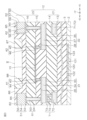
- FIG. 1 is a schematic plan view showing an electronic component according to an embodiment of the present invention, and is a plan view showing a form in which a resistance layer is incorporated.
- FIG. 2 is a sectional view taken along the line II-II shown in FIG.
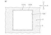
- FIG. 3 is an enlarged view of region III in FIG.
- FIG. 4 is an enlarged plan view for explaining the planar shape of the resistance layer.
- FIG. 5 is an enlarged plan view showing a part of the first main surface of the semiconductor layer.
- FIG. 6A is a cross-sectional view showing a part of the manufacturing process of the electronic component shown in FIG. 1, and is a cross-sectional view corresponding to the cut plane of FIG. 2.
- FIG. FIG. 6B is a cross-sectional view showing the next step of FIG. 6A.
- FIG. 6C is a cross-sectional view showing the next step of FIG. 6B.
- FIG. 6D is a cross-sectional view showing the next step of FIG. 6C.
- FIG. 6E is a cross-sectional view showing the next step of FIG. 6D.
- FIG. 6F is a cross-sectional view showing the next step of FIG. 6E.
- FIG. 6G is a cross-sectional view showing the next step of FIG. 6F.
- FIG. 6H is a cross-sectional view showing the next step of FIG. 6G.
- FIG. 6I is a cross-sectional view showing the next step of FIG. 6H.
- FIG. 6J is a cross-sectional view showing the next step of FIG. 6I.
- FIG. 6K is a cross-sectional view showing the next step of FIG. 6J.
- FIG. 6L is a cross-sectional view showing the next step of FIG. 6K.
- FIG. 6M is a cross-sectional view showing the next step from FIG. 6L.
- FIG. 6L is a cross-sectional view showing the next step of FIG. 6M.
- FIG. 6O is a cross-sectional view showing the next step of FIG. 6N.
- FIG. 6P is a cross-sectional view showing the next step of FIG. 6O.
- FIG. 6Q is a cross-sectional view showing the next step of FIG. 6P.
- FIG. 6R is a cross-sectional view showing the next step of FIG. 6Q.
- FIG. 6S is a cross-sectional view showing the next step of FIG. 6R.
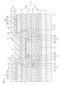
- FIG. 7 is a plan view for explaining the uneven structure of the first sample.
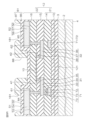
- FIG. 8 is a plan view for explaining the uneven structure of the second to seventh samples.
- FIG. 9 is a plan view for explaining the uneven structure of the eighth and ninth samples.
- FIG. 10 is a plan view for explaining the uneven structure of the tenth and eleventh samples.
- FIG. 11 is a plan view for explaining the uneven structure of the 12th and 13th samples.
- An embodiment of the present disclosure includes a semiconductor layer having a first main surface and a second main surface opposite to the first main surface, a lower insulating layer formed on the first main surface of the semiconductor layer, and a lower insulating layer formed on the first main surface of the semiconductor layer; a resistance layer formed on the insulating layer and having a notch extending in a predetermined first direction from a part of the periphery thereof; and an upper insulating layer formed on the lower insulating layer so as to cover the resistance layer.
- an electronic component that includes a plurality of grooves arranged at equal intervals in a second direction perpendicular to the direction and extending parallel to the first direction, and a convex portion that is a portion between two adjacent grooves. .
- the resistance layer has a first opposing side made up of two sides parallel to the second direction and a second opposing side made up of two two sides parallel to the first direction in plan view.
- the cutout portion extends from a mid-length portion of one of the first opposing sides toward the other of the first opposing sides.
- An embodiment of the present disclosure includes a first via electrode embedded in the lower insulating layer and having an upper end connected to a portion of the resistive layer near one of the second opposing sides; a second via electrode embedded in the insulating layer and having an upper end connected to a portion of the resistive film near the other of the second opposing sides.
- An embodiment of the present disclosure includes a first lower wiring layer formed in a region on the lower insulating layer side with respect to the resistive layer and electrically connected to the first via electrode; and a second lower wiring layer formed in a region on the lower insulating layer side and electrically connected to the second via electrode.
- the first lower wiring layer extends from the inside to the outside of the resistance layer with respect to one of the second opposing sides in a plan view
- the second lower wiring layer extends from the inside to the outside of the resistance layer with respect to the other of the second opposing sides in a plan view, and connects the first lower wiring layer and the second lower wiring layer.
- the side wiring layers are arranged at intervals in the second direction in plan view.
- the resistance layer is connected in series to the first lower wiring layer and the second lower wiring layer.
- An embodiment of the present disclosure includes a first upper wiring layer formed on the upper insulating layer and electrically connected to the first lower wiring layer; and a second upper wiring layer electrically connected to the lower wiring layer.
- the resistance layer is connected in series to the first upper wiring layer and the second upper wiring layer.
- a first long via penetrates through the upper insulating layer and a part of the lower insulating layer and is electrically connected to the first lower wiring layer and the first upper wiring layer.
- a second long via electrode that penetrates through the upper insulating layer and part of the lower insulating layer and is electrically connected to the second lower wiring layer and the second upper wiring layer.
- the resistance layer is located in a straight line connecting the first long via electrode and the second long via electrode in plan view.
- the semiconductor layer includes a device region in which a functional device is formed and an outer region outside the device region, and the resistive layer is formed in the outer region in plan view.
- the resistance layer is made of a metal thin film containing at least one of CrSi, CrSiO, and CrSiN.
- the depth of the groove is 100 nm or more and 300 nm or less, and the width of the groove and the interval between the grooves are 0.2 ⁇ m or more and 1 ⁇ m or less.
- the depth of the groove is 150 nm or more and 300 nm or less, and the width of the groove and the interval between the grooves are 0.2 ⁇ m or more and 1 ⁇ m or less.
- the lower insulating layer includes a plurality of laminated lower silicon oxide films
- the upper insulating layer is formed on the lower insulating layer to cover the resistive film. includes an upper silicon oxide film.
- An embodiment of the present disclosure includes a step of forming an uneven structure in a predetermined region of the first main surface of a semiconductor layer having a first main surface and a second main surface opposite thereto; forming a lower insulating film on the main surface; forming a resistive layer on the lower insulating film; and forming an upper insulating film on the lower insulating film so as to cover the resistive layer.
- the predetermined region is a region including at least a region immediately below the resistance layer on the first main surface of the semiconductor layer, and in the step of forming the uneven structure, the predetermined region is The uneven structure is formed by forming a plurality of grooves extending parallel to the first direction at regular intervals in a second direction perpendicular to the first direction.
- FIG. 1 is a schematic plan view showing an electronic component 1 according to an embodiment of the present invention, and is a plan view showing a form in which a resistance layer 10 is incorporated.
- the +X direction is a predetermined direction along the surface of the semiconductor layer 2 in a plan view
- the +Y direction is a direction along the surface of the semiconductor layer 2 in a plan view and is orthogonal to the +X direction
- the -X direction is the opposite direction to the +X direction
- the -Y direction is the opposite direction to the +Y direction.
- the electronic component 1 is a semiconductor device including various functional devices formed using a conductive material, a semiconductor material, or the properties of a semiconductor material.
- the electronic component 1 includes a chip-shaped semiconductor layer 2 formed in the shape of a rectangular parallelepiped.
- the semiconductor layer 2 includes a first main surface 3 on one side, a second main surface 4 on the other side, and side surfaces 5A, 5B, 5C, and 5D connecting the first main surface 3 and the second main surface 4.
- the first main surface 3 is a device formation surface.
- the first principal surface 3 and the second principal surface 4 are formed into a rectangular shape (in this embodiment, a square shape) in a plan view (hereinafter simply referred to as "plan view") seen from the normal direction thereof. .
- the semiconductor layer 2 may be a Si semiconductor layer containing Si (silicon) as an example of a semiconductor material.
- the Si semiconductor layer may have a stacked structure including a Si semiconductor substrate and a Si epitaxial layer.
- the Si semiconductor layer may have a single layer structure made of a Si semiconductor substrate.
- the semiconductor layer 2 is made of a Si semiconductor substrate.
- the semiconductor layer 2 may be a SiC semiconductor layer containing SiC (silicon carbide) as an example of a semiconductor material.
- the SiC semiconductor layer may have a stacked structure including a SiC semiconductor substrate and a SiC epitaxial layer.
- the SiC semiconductor layer may have a single layer structure made of a SiC semiconductor substrate.
- the semiconductor layer 2 may be a compound semiconductor layer containing a compound semiconductor material as an example of a semiconductor material.
- the compound semiconductor layer may have a stacked structure including a compound semiconductor substrate and a compound semiconductor epitaxial layer.
- the compound semiconductor layer may have a single layer structure made of a compound semiconductor substrate.
- the compound semiconductor material may be a III-V compound semiconductor material.
- the semiconductor layer 2 contains at least one of AlN (aluminum nitride), InN (indium nitride), GaN (gallium nitride), and GaAs (gallium arsenide), which are examples of III-V compound semiconductor materials. Good too.
- the semiconductor layer 2 includes a device region 6 and an outer region 7.
- the device area 6 is an area where functional devices are formed.
- the device region 6 is formed at intervals from the side surfaces 5A to 5D of the semiconductor layer 2 in the inner region.
- the device region 6 is formed into an L-shape in plan view.
- the planar shape of the device region 6 is arbitrary and is not limited to the planar shape shown in FIG.
- a functional device is formed in the semiconductor layer 2. More specifically, the functional device is formed using the first main surface 3 of the semiconductor layer 2 and/or the surface layer portion of the first main surface 3.
- the functional device may include at least one of a passive device, a semiconductor rectifying device, and a semiconductor switching device. Passive devices may include semiconductor passive devices.
- the passive device may include at least one of a resistor, a capacitor, and a coil.
- the semiconductor rectifier device may include at least one of a pn junction diode, a Zener diode, a Schottky barrier diode, and a fast recovery diode.
- the semiconductor switching device may include at least one of a BJT (Bipolar Junction Transistor), a MISFET (Metal Insulator Field Effect Transistor), an IGBT (Insulated Gate Bipolar Junction Transistor), and a JFET (Junction Field Effect Transistor). good.
- BJT Bipolar Junction Transistor
- MISFET Metal Insulator Field Effect Transistor
- IGBT Insulated Gate Bipolar Junction Transistor
- JFET Joint Field Effect Transistor
- the functional device may include a circuit network in which at least two of a passive device (semiconductor passive device), a semiconductor rectifier device, and a semiconductor switching device are selectively combined.
- the circuitry may form part or all of an integrated circuit.
- the integrated circuit may include SSI (Small Scale Integration), LSI (Large Scale Integration), MSI (Medium Scale Integration), VLSI (Very Large Scale Integration), and ULSI (Ultra-Very Large Scale Integration).
- SSI Small Scale Integration
- LSI Large Scale Integration
- MSI Medium Scale Integration
- VLSI Very Large Scale Integration
- ULSI Ultra-Very Large Scale Integration
- the outer area 7 is an area outside the device area 6.
- the outer region 7 does not contain any functional devices.
- the outer region 7 is divided into a region between the side surfaces 5A to 5D of the semiconductor layer 2 and the device region 6.
- the outer region 7 is formed into a rectangular shape in plan view.
- the planar shape of the outer region 7 is arbitrary and is not limited to the planar shape shown in FIG.
- the arrangement and planar shape of the outer region 7 are arbitrary and are not limited to the arrangement and planar shape shown in FIG.
- the outer region 7 may be formed at the center of the first main surface 3 in plan view.
- a resistance circuit 11 including a resistance layer 10 made of a metal thin film is formed in the outer region 7 at a distance from the first main surface 3 of the semiconductor layer 2. That is, in this embodiment, the resistance circuit 11 (resistance layer 10) is formed avoiding the device region 6 in plan view. The resistance circuit 11 (resistance layer 10) is electrically connected to the functional device.
- the resistance circuit 11 (resistance layer 10) in the outer region 7, the electrical influence of the resistance circuit 11 on the device region 6 is suppressed, and the electrical influence of the device region 6 on the resistance circuit 11 is suppressed. can.
- parasitic capacitance between device region 6 and resistance circuit 11 can be suppressed. In other words, it is possible to reduce noise and improve the Q value.
- the resistance circuit 11 includes one resistance layer 10
- the resistance circuit 11 may include a plurality of (two or more) resistance layers 10.
- the resistance layer 10 resistance circuit 11
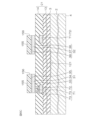
- FIG. 2 is a sectional view taken along the line II-II shown in FIG. 1.
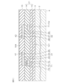
- FIG. 3 is an enlarged view of region III in FIG.
- FIG. 4 is a plan view for explaining the planar shape of the resistance layer 10.
- FIG. 5 is an enlarged plan view showing a part of the first main surface of the semiconductor layer.
- a multilayer wiring structure 12 is formed on the first main surface 3 of the semiconductor layer 2.
- the multilayer wiring structure 12 has a laminated structure in which a plurality of insulating layers are stacked, and includes a plurality of wiring layers selectively formed within the plurality of insulating layers.
- the multilayer wiring structure 12 includes, for example, a first insulating layer 13, a second insulating layer 14, a third insulating layer 15, and a fourth insulating layer 16, which are laminated in this order from the first main surface 3 side of the semiconductor layer 2.
- the terms “first,” “second,” “third,” and “fourth” regarding the first to fourth insulating layers 13 to 16 are used to identify the insulating layers in the drawings. , not intended to be permuted.
- the number of laminated insulating layers in the multilayer wiring structure 12 is arbitrary and is not limited to the number of laminated layers shown in FIG. 2. Therefore, the multilayer wiring structure 12 may include less than four insulating layers, or may include five or more insulating layers.
- the first to fourth insulating layers 13 to 16 each have a main surface.
- the main surfaces of the first to fourth insulating layers 13 to 16 are each formed flat.
- the main surfaces of the first to fourth insulating layers 13 to 16 extend parallel to the first main surface 3 of the semiconductor layer 2, respectively.
- the main surfaces of the first to fourth insulating layers 13 to 16 may each be a ground surface.
- the fourth insulating layer 16 is an example of an "upper insulating layer" in the present disclosure.
- the insulating layers 13, 14, and 15 interposed between the semiconductor layer 2 and the fourth insulating layer 16 correspond to "lower insulating layers" in the present disclosure.
- the first to fourth insulating layers 13 to 16 may each have a laminated structure including a silicon oxide film and a silicon nitride film.
- a silicon nitride film may be formed on the silicon oxide film, or a silicon oxide film may be formed on the silicon nitride film.
- the first to fourth insulating layers 13 to 16 may each have a single layer structure made of a silicon oxide film or a silicon nitride film.
- the first to fourth insulating layers 13 to 16 are preferably formed of the same type of insulating material.
- the first to fourth insulating layers 13 to 16 each have a single layer structure made of a silicon oxide film.
- the thickness of the first to fourth insulating layers 13 to 16 may be 100 nm or more and 3500 nm or less, respectively.
- the thickness of the first to fourth insulating layers 13 to 16 is 100 nm or more and 500 nm or less, 500 nm or more and 1000 nm or less, 1000 nm or more and 1500 nm or less, 1500 nm or more and 2000 nm or less, 2000 nm or more and 2500 nm or less, or 2500 nm or more and 3000 nm or less, or 3000 nm, respectively. It may be greater than or equal to 3500 nm or less.
- the thickness of the first to fourth insulating layers 13 to 16 is preferably 100 nm or more and 1500 nm or less, respectively.
- the thicknesses of the first to fourth insulating layers 13 to 16 may be equal to each other or may be different from each other.
- the multilayer wiring structure 12 includes a connection circuit formation layer 21 and a resistance circuit formation layer 22 that are formed in different layers.
- connection circuit formation layer 21 is formed on the first main surface 3 side of the semiconductor layer 2.
- the connection circuit forming layer 21 includes a first insulating layer 13 and a second insulating layer 14.
- the connection circuit forming layer 21 is a layer whose purpose is to electrically connect the device region 6 (functional device) and the outer region 7 (resistance circuit 11). The specific structure of the connection circuit forming layer 21 will be described later.
- the resistance circuit formation layer 22 is formed on the connection circuit formation layer 21.
- the resistance circuit formation layer 22 includes a third insulating layer 15 and a fourth insulating layer 16.
- the resistance circuit formation layer 22 is a layer whose one purpose is to form the resistance circuit 11 (resistance layer 10) in the outer region 7.
- the resistance circuit 11 includes a first lower wiring layer 31 , a second lower wiring layer 32 , a resistance layer 10 , a first via electrode 41 , a second via electrode 42 , a first upper wiring layer 51 , and a second upper wiring layer 52 , a first long via electrode 61 and a second long via electrode 62.
- the first lower wiring layer 31 and the second lower wiring layer 32 are arranged on the connection circuit forming layer 21 (second insulating layer 14) with an interval in the X direction.
- the first lower wiring layer 31 and the second lower wiring layer 32 are covered with the third insulating layer 15.
- the first lower wiring layer 31 has a laminated structure in which a plurality of electrode layers are laminated.
- the first lower wiring layer 31 includes a first barrier layer 33, a main body layer 34, and a second barrier layer 35, which are laminated in this order from above the connection circuit forming layer 21 (fourth insulating layer 16).
- the first barrier layer 33 has a stacked structure including a Ti layer and a TiN layer stacked in this order from above the connection circuit forming layer 21 (second insulating layer 14).
- the first barrier layer 33 may have a single layer structure consisting of a Ti layer or a TiN layer.
- the main body layer 34 has a resistance value that is less than the resistance value of the first barrier layer 33 and the resistance value of the second barrier layer 35.
- the main body layer 34 has a thickness that exceeds the thickness of the first barrier layer 33 and the thickness of the second barrier layer 35.
- the main body layer 34 may contain at least one of Al, Cu, an AlSiCu alloy, an AlSi alloy, and an AlCu alloy.
- the main body layer 34 has a single layer structure consisting of an AlCu alloy layer.
- the second barrier layer 35 has a laminated structure including a Ti layer and a TiN layer laminated in this order from above the main body layer 34.
- the second barrier layer 35 may have a single layer structure consisting of a Ti layer or a TiN layer.
- the second lower wiring layer 32 is arranged on the +X side with respect to the second lower wiring layer 32.
- the second lower wiring layer 32 has a laminated structure in which a plurality of electrode layers are laminated.
- the second lower wiring layer 32 includes a first barrier layer 36, a main body layer 37, and a second barrier layer 38, which are laminated in this order from above the connection circuit forming layer 21 (second insulating layer 14).
- the first barrier layer 36 has a stacked structure including a Ti layer and a TiN layer stacked in this order from above the connection circuit forming layer 21 (second insulating layer 14).
- the first barrier layer 36 may have a single layer structure consisting of a Ti layer or a TiN layer.
- the main body layer 37 has a resistance value that is less than the resistance value of the first barrier layer 36 and the resistance value of the second barrier layer 38.
- Body layer 37 has a thickness that exceeds the thickness of first barrier layer 36 and the thickness of second barrier layer 38 .
- the main body layer 37 may contain at least one of Al, Cu, AlSiCu alloy, AlSi alloy, and AlCu alloy.
- the main body layer 37 has a single layer structure consisting of an AlCu alloy layer.
- the second barrier layer 38 has a laminated structure including a Ti layer and a TiN layer laminated in this order from above the main body layer 37.
- the second barrier layer 38 may have a single layer structure consisting of a Ti layer or a TiN layer.
- the resistance layer 10 is arranged on the third insulating layer 15. As shown in FIG. 4, the resistance layer 10 has a rectangular shape (rectangular shape) long in the X direction in plan view, and has a pair of first opposing sides 101 parallel to the X direction and a pair of first opposing sides 101 parallel to the Y direction. It has two opposing sides 102. The resistance layer 10 is arranged so as to straddle the first lower wiring layer 31 and the second lower wiring layer 32 in a plan view.
- the resistance layer 10 includes a first end 10a on the ⁇ X side, a second end 10b on the +X side, and a connecting portion 10c that connects the first end 10a and the second end 10b.
- the first end 10a of the resistance layer 10 is arranged on the +X side end of the surface of the first lower wiring layer 31.
- the second end 10b of the resistance layer 10 is arranged on the -X side end of the surface of the second lower wiring layer 32.
- the resistance layer 10 includes one notch 110 formed in the connection portion 10c.
- the cutout portion 110 extends in a direction (Y direction) that intersects the direction in which the connecting portion 10c extends. In this embodiment, the cutout portion 110 extends in the Y direction from one side 101 of the first opposing sides 101 parallel to the X direction in the resistance layer 10 toward the other side 101. Note that the cutout portion 110 is omitted in FIGS. 1 to 3.
- the notch 110 is a laser beam machining mark where a part of the connecting portion 10c is cut by laser beam irradiation.
- the cutout portion 110 extends the current path in the resistance layer 10 . This increases the resistance value of the resistance layer 10.
- the resistance value of the resistance layer 10 can be adjusted in an increasing direction by the notch 110.
- the connecting portion 10c extends in a band shape in the area between the first end 10a and the second end 10b.
- the connecting portion 10c extends in a band shape along a straight line connecting the first end 10a and the second end 10b.
- the first end 10a, the second end 10b, and the connection portion 10c of the resistance layer 10 are formed to have a uniform width.
- the resistance layer 10 is preferably made of a metal thin film containing at least one of CrSi (chromium silicon alloy), CrSiO (chromium silicon oxide alloy), and CrSiN (chromium silicon nitride alloy). It is particularly preferable that the resistance layer 10 contains CrSi.
- the resistance layer 10 may have a single layer structure made of a CrSi film, a CrSiO film, or a CrSiN film. In this embodiment, the resistance layer 10 has a single layer structure made of a CrSi film.
- the resistance layer 10 may be composed of a metal thin film containing at least one of CrSi (chromium silicon alloy), TaN (tantalum nitride), and TiN (titanium nitride).
- the resistance layer 10 may have a single layer structure made of a TaN film or a TiN film.
- the resistance layer 10 may have a laminated structure including a CrSi film and a TaN film laminated in any order.
- the resistance layer 10 may have a laminated structure including a CrSi film and a TiN film laminated in any order.
- the resistance layer 10 may have a laminated structure including a TaN film and a TiN film laminated in any order.
- the resistance layer 10 may have a stacked structure including a CrSi film, a TaN film, and a TiN film stacked in any order.
- the thickness of the resistance layer 10 may be 0.1 nm or more and 100 nm or less.
- the thickness of the resistance layer 10 is 0.1 nm or more and 10 nm or less, 10 nm or more and 20 nm or less, 20 nm or more and 30 nm or less, 30 nm or more and 40 nm or less, 40 nm or more and 50 nm or less, 50 nm or more and 60 nm or less, 60 nm or more and 70 nm or less, 70 nm or more and 80 nm or less, It may be 80 nm or more and 90 nm or less, or 90 nm or more and 100 nm or less.
- the thickness of the resistance layer 10 is preferably 1 nm or more and 20 nm or less.
- the resistance layer 10 is interposed in a region between the third insulating layer 15 and the fourth insulating layer 16. More specifically, the resistance layer 10 is formed in a film shape on the main surface of the third insulating layer 15. On the main surface of the third insulating layer 15, no film-like or layer-like wiring other than the resistance layer 10 is formed in the device region 6 and the outer region 7. The third insulating layer 15 is provided to form the resistance layer 10.
- the resistive layer 10 By arranging the resistive layer 10 in the outer region 7, the electrical influence of the resistive layer 10 on the device region 6 can be suppressed, and the electrical influence of the device region 6 on the resistive layer 10 can be suppressed. For example, parasitic capacitance between device region 6 and resistance layer 10 can be suppressed. In other words, it is possible to reduce noise and improve the Q value.
- the first via electrode 41 is electrically connected to the resistance layer 10 and the first lower wiring layer 31.
- the second via electrode 42 is electrically connected to the resistance layer 10 and the second lower wiring layer 32.
- the first via electrode 41 is embedded in the third insulating layer 15 and exposed from the main surface of the third insulating layer 15.
- the second via electrode 42 is embedded in the third insulating layer 15 at a distance from the first via electrode 41 in the X direction, and is exposed from the main surface of the third insulating layer 15 .
- the second via electrode 42 is arranged on the +X side with respect to the first via electrode 41.
- the upper end of the first via electrode 41 is electrically connected to the first end 10a of the resistance layer 10.
- the lower end of the first via electrode 41 is electrically connected to the +X side end of the first lower wiring layer 31 .
- the upper end of the second via electrode 42 is electrically connected to the second end 10b of the resistance layer 10.
- the lower end of the second via electrode 42 is electrically connected to the -X side end of the second lower wiring layer 32.
- the resistance layer 10 is electrically connected to the first via electrode 41 and the second via electrode 42. Further, the first end portion 10a of the resistance layer 10 is electrically connected to the first lower wiring layer 31 via the first via electrode 41. Further, the second end portion 10b of the resistance layer 10 is electrically connected to the second lower wiring layer 32 via the second via electrode 42. Thereby, the resistance layer 10 is connected in series to the first lower wiring layer 31 and the second lower wiring layer 32.
- the first via electrode 41 is formed into a circular shape in plan view.
- the planar shape of the first via electrode 41 is arbitrary.
- the first via electrode 41 may be formed into a polygonal shape such as a triangular, quadrangular, or hexagonal shape, or an elliptical shape in plan view, instead of a circular shape.
- the first via electrode 41 is formed in a tapered shape whose width narrows from the upper end toward the lower end when viewed in cross section.
- the first via electrode 41 has a laminated structure including a main body layer 43 and a barrier layer 44.
- the main body layer 43 is embedded in the third insulating layer 15 .
- the main body layer 43 may contain tungsten (W) or copper (Cu).
- the main body layer 43 has a single layer structure made of a tungsten layer.
- the barrier layer 44 is interposed between the third insulating layer 15 and the main body layer 43.
- the barrier layer 44 has a laminated structure in which a plurality of electrode layers are laminated.
- the barrier layer 44 includes a Ti layer and a TiN layer formed in this order from the third insulating layer 15.
- the barrier layer 44 may have a single layer structure consisting of a Ti layer or a TiN layer.
- the second via electrode 42 is formed into a circular shape in plan view.
- the planar shape of the second via electrode 42 is arbitrary.
- the second via electrode 42 may be formed into a polygonal shape such as a triangular, quadrangular, or hexagonal shape, or an elliptical shape in plan view, instead of a circular shape.
- the second via electrode 42 is formed in a tapered shape whose width narrows from the upper end toward the lower end in a cross-sectional view.
- the second via electrode 42 has a laminated structure including a main body layer 45 and a barrier layer 46.
- the main body layer 45 is embedded in the third insulating layer 15 .
- Main body layer 45 may include tungsten (W) or copper (Cu).
- the main body layer 45 has a single layer structure made of a tungsten layer.
- the barrier layer 46 is interposed between the third insulating layer 15 and the main body layer 45.
- the barrier layer 46 has a laminated structure in which a plurality of electrode layers are laminated.
- the barrier layer 46 includes a Ti layer and a TiN layer formed in this order from the third insulating layer 15.
- the barrier layer 46 may have a single layer structure consisting of a Ti layer or a TiN layer.
- the first upper wiring layer 51 is formed on the fourth insulating layer 16.
- the first upper wiring layer 51 forms one of the uppermost wiring layers of the multilayer wiring structure 12.
- the first upper wiring layer 51 is electrically connected to the first lower wiring layer 31.
- the second upper wiring layer 52 is formed on the fourth insulating layer 16 at a distance from the first upper wiring layer 51 in the X direction.
- the first upper wiring layer 51 is arranged on the -X side with respect to the resistance layer 10
- the second upper wiring layer 52 is arranged on the +X side with respect to the resistance layer 10.
- the second upper wiring layer 52 forms one of the uppermost wiring layers of the multilayer wiring structure 12.
- the second upper wiring layer 52 is electrically connected to the second lower wiring layer 32.
- the resistance layer 10 is electrically connected to the first upper wiring layer 51 via the first lower wiring layer 31. Further, the resistance layer 10 is electrically connected to the second upper wiring layer 52 via the second lower wiring layer 32. The resistance layer 10 is connected in series to the first upper wiring layer 51 and the second upper wiring layer 52 via the first lower wiring layer 31 and the second lower wiring layer 32 .
- the first upper wiring layer 51 is formed at a distance from the resistance layer 10 in plan view.
- the first upper wiring layer 51 does not overlap the resistance layer 10 in plan view.
- the entire resistance layer 10 is exposed from the first upper wiring layer 51 in plan view.
- the second upper wiring layer 52 is formed at a distance from the resistance layer 10 in plan view.
- the second upper wiring layer 52 does not overlap the resistance layer 10 in plan view.
- the entire resistance layer 10 is exposed from the second upper wiring layer 52 in plan view.
- the resistance layer 10 is formed in a region between the first upper wiring layer 51 and the second upper wiring layer 52 in plan view. Thereby, parasitic capacitance can be suppressed in the region between the resistance layer 10 and the first upper wiring layer 51. Furthermore, parasitic capacitance can be suppressed in the region between the resistance layer 10 and the second upper wiring layer 52.
- the resistance layer 10 is formed at a distance from the first upper wiring layer 51 and the second upper wiring layer 52 in plan view. Thereby, parasitic capacitance can be appropriately suppressed in the region between the resistance layer 10 and the first upper wiring layer 51. Furthermore, parasitic capacitance can be appropriately suppressed in the region between the resistance layer 10 and the second upper wiring layer 52.
- the thickness of the first upper wiring layer 51 and the second upper wiring layer 52 may be 100 nm or more and 15000 nm or less.
- the thickness of the first upper wiring layer 51 and the second upper wiring layer 52 is 100 nm or more and 1500 nm or less, 1500 nm or more and 3000 nm or less, 3000 nm or more and 4500 nm or less, 4500 nm or more and 6000 nm or less, 6000 nm or more and 7500 nm or less, 7500 nm or more and 9000 nm or less, and 9000 nm or more.
- the thickness of the first upper wiring layer 51 and the second upper wiring layer 52 is approximately 2200 nm.
- the first upper wiring layer 51 has a laminated structure in which a plurality of electrode layers are laminated.
- the first upper wiring layer 51 includes a first barrier layer 53, a main body layer 54, and a second barrier layer 55, which are laminated in this order from above the fourth insulating layer 16.
- the first barrier layer 53 has a stacked structure including a Ti layer and a TiN layer stacked in this order from above the fourth insulating layer 16.
- the first barrier layer 53 may have a single layer structure consisting of a Ti layer or a TiN layer.
- the main body layer 54 has a resistance value that is less than the resistance value of the first barrier layer 53 and the resistance value of the second barrier layer 55.
- the main body layer 54 has a thickness that exceeds the thickness of the first barrier layer 53 and the thickness of the second barrier layer 55.
- the main body layer 54 may contain at least one of Al, Cu, AlSiCu alloy, AlSi alloy, and AlCu alloy.
- the main body layer 54 has a single layer structure made of an AlCu alloy layer.
- the second barrier layer 55 has a laminated structure including a Ti layer and a TiN layer laminated in this order from above the main body layer 54.
- the second barrier layer 55 may have a single layer structure consisting of a Ti layer or a TiN layer.
- the second upper wiring layer 52 has a laminated structure in which a plurality of electrode layers are laminated.
- the second upper wiring layer 52 includes a first barrier layer 56, a main body layer 57, and a second barrier layer 58, which are laminated in this order from above the fourth insulating layer 16.
- the first barrier layer 56 has a stacked structure including a Ti layer and a TiN layer stacked in this order from above the fourth insulating layer 16.
- the first barrier layer 56 may have a single layer structure consisting of a Ti layer or a TiN layer.
- the main body layer 57 has a resistance value that is less than the resistance value of the first barrier layer 56 and the resistance value of the second barrier layer 58.
- Body layer 57 has a thickness that exceeds the thickness of first barrier layer 56 and the thickness of second barrier layer 58.
- the main body layer 57 may contain at least one of Al, Cu, AlSiCu alloy, AlSi alloy, and AlCu alloy.
- the main body layer 57 has a single-layer structure made of an AlCu alloy layer.
- the second barrier layer 58 has a laminated structure including a Ti layer and a TiN layer laminated in this order from above the main body layer 57.
- the second barrier layer 58 may have a single layer structure consisting of a Ti layer or a TiN layer.
- the first long via electrode 61 is electrically connected to the first lower wiring layer 31 and the first upper wiring layer 51.
- the second long via electrode 62 is electrically connected to the second lower wiring layer 32 and the second upper wiring layer 52.
- the resistance layer 10 is electrically connected to the first upper wiring layer 51 via the first via electrode 41, the first lower wiring layer 31, and the first long via electrode 61. Further, the resistance layer 10 is electrically connected to the second upper wiring layer 52 via the second via electrode 42, the second lower wiring layer 32, and the second long via electrode 62.
- the first long via electrode 61 is formed on the side (-X side) of the resistance layer 10. In this embodiment, the first long via electrode 61 is located on a straight line connecting the first via electrode 41 and the second via electrode 42.
- the second long via electrode 62 is formed on the side (+X side) of the resistance layer 10 at a distance from the first long via electrode 61 in the X direction. In this embodiment, the second long via electrode 62 faces the first long via electrode 61 with the resistance layer 10 in between. The second long via electrode 62 is located on a straight line connecting the first via electrode 41 and the second via electrode 42.
- the resistance layer 10 is located on the straight line connecting the first long via electrode 61 and the second long via electrode 62.
- the resistance layer 10 is located on a straight line connecting the first via electrode 41, the second via electrode 42, the first long via electrode 61, and the second long via electrode 62.
- the resistance layer 10 extends along a straight line connecting the first long via electrode 61 and the second long via electrode 62.
- the first long via electrode 61 is formed into a circular shape in plan view.
- the planar shape of the first long via electrode 61 is arbitrary.
- the first long via electrode 61 may be formed into a polygonal shape such as a triangular, quadrangular, or hexagonal shape, or an elliptical shape in plan view, instead of a circular shape.
- the first long via electrode 61 penetrates the third insulating layer 15 and the fourth insulating layer 16, is embedded in the third insulating layer 15 and the fourth insulating layer 16, and is exposed from the main surface of the fourth insulating layer 16. .
- the upper end of the first long via electrode 61 is electrically connected to the +X direction end of the first upper wiring layer 51.
- the lower end of the first long via electrode 61 is electrically connected to the ⁇ X direction end of the first lower wiring layer 31.
- the first long via electrode 61 is formed in a tapered shape whose width narrows from the upper end toward the lower end in a cross-sectional view.
- the first long via electrode 61 has a laminated structure including a main body layer 63 and a barrier layer 64.
- the main body layer 63 is embedded in the third insulating layer 15 and the fourth insulating layer 16.
- the main body layer 63 may contain tungsten (W) or copper (Cu).
- the main body layer 63 has a single layer structure made of a tungsten layer.
- the barrier layer 64 is interposed between the main body layer 63 and the third insulating layer 15 and between the main body layer 63 and the fourth insulating layer 16.
- the barrier layer 64 has a laminated structure in which a plurality of electrode layers are laminated.
- the barrier layer 64 includes a Ti layer and a TiN layer formed in this order starting from the third insulating layer 15.
- the barrier layer may have a single layer structure consisting of a Ti layer or a TiN layer.
- the second long via electrode 62 is formed into a circular shape in plan view.
- the planar shape of the second long via electrode 62 is arbitrary.
- the second long via electrode 62 may be formed into a polygonal shape such as a triangular, quadrangular, or hexagonal shape, or an elliptical shape in plan view, instead of a circular shape.
- the second long via electrode 62 penetrates the third insulating layer 15 and the fourth insulating layer 16, is embedded in the third insulating layer 15 and the fourth insulating layer 16, and is exposed from the main surface of the fourth insulating layer 16. .
- the upper end of the second long via electrode 62 is electrically connected to the -X side end of the second upper wiring layer 52.
- the lower end of the second long via electrode 62 is electrically connected to the +X side end of the second lower wiring layer 32.
- the second long via electrode 62 is formed in a tapered shape whose width narrows from the upper end toward the lower end in a cross-sectional view.
- the second long via electrode 62 has a laminated structure including a main body layer 65 and a barrier layer 66.
- the main body layer 65 is embedded in the third insulating layer 15 and the fourth insulating layer 16.
- the main body layer 65 may include tungsten (W) or copper (Cu).
- the main body layer 65 has a single layer structure made of a tungsten layer.
- the barrier layer 66 is interposed between the main body layer 65 and the third insulating layer 15 and between the main body layer 65 and the fourth insulating layer 16.
- the barrier layer 66 has a laminated structure in which a plurality of electrode layers are laminated.
- the barrier layer 66 includes a Ti layer and a TiN layer formed in this order starting from the third insulating layer 15.
- the barrier layer 66 may have a single layer structure consisting of a Ti layer or a TiN layer.
- connection circuit forming layer 21 includes wiring 71 that electrically connects the functional device and the resistance layer 10.
- the wiring 71 is selectively formed in the first insulating layer 13 and the second insulating layer 14 and routed from the device region 6 to the outer region 7 .
- the wiring 71 includes one or more connection wiring layers 72 electrically connected to the functional devices in the device region 6.
- One or more connection wiring layers 72 are formed on either or both of the first insulating layer 13 and the second insulating layer 14 .
- FIG. 2 shows an example in which two connection wiring layers 72 are formed on the first insulating layer 13.
- connection wiring layers 72 are selectively routed from the device region 6 to the outer region 7.
- the connection wiring layer 72 has the same laminated structure as the first lower wiring layer 31 (second lower wiring layer 32) and the first upper wiring layer 51 (second upper wiring layer 52). A detailed description of the connection wiring layer 72 will be omitted.
- the wiring 71 includes one or more connection via electrodes 73.
- One or more connection via electrodes 73 connect one or more connection wiring layers 72 to any first lower wiring layer 31 (second lower wiring layer 32) or any first upper wiring layer 51 (second lower wiring layer 32). 2 upper wiring layer 52).
- connection via electrodes 73 are formed on either or both of the first insulating layer 13 and the second insulating layer 14.
- FIG. 2 shows an example in which one connection wiring layer 72 is connected to the first lower wiring layer 31 by two connection via electrodes 73.
- connection via electrode 73 has the same laminated structure as the first via electrode 41 (second via electrode 42) and the first long via electrode 61 (second long via electrode 62). A detailed description of the connection via electrode 73 will be omitted.
- a top insulating layer 81 is formed on the multilayer wiring structure 12.
- the uppermost insulating layer 81 selectively covers the first upper wiring layer 51 and the second upper wiring layer 52.
- the uppermost insulating layer 81 covers the connection portion between the first upper wiring layer 51 and the first long via electrode 61 in a plan view.
- the uppermost insulating layer 81 covers the connection portion between the second upper wiring layer 52 and the second long via electrode 62 in plan view.
- a first pad opening 82 and a second pad opening 83 are formed in the uppermost insulating layer 81 in the outer region 7 .
- the first pad opening 82 exposes a part of the first upper wiring layer 51 as a first pad region 84 . More specifically, the first pad opening 82 exposes a region of the first upper wiring layer 51 other than the connecting portion between the first upper wiring layer 51 and the first long via electrode 61 as a first pad region 84. .
- the second pad opening 83 exposes a part of the second upper wiring layer 52 as a second pad region 85. More specifically, the second pad opening 83 exposes a region of the second upper wiring layer 52 other than the connecting portion between the second upper wiring layer 52 and the second long via electrode 62 as a second pad region 85. .
- the uppermost insulating layer 81 has a laminated structure including a passivation layer 86 and a resin layer 87.
- the resin layer 87 is shown by hatching for clarity.
- An opening 88 for laser trimming for forming a notch 110 in the resistance layer 10 is formed in the resin layer 87 in a region between the first upper wiring layer 51 and the second upper wiring layer 52 in plan view. There is.
- the opening 88 is formed directly above a region of the resistance layer 10 including the connection portion 10c and its peripheral portion.
- the passivation layer 86 may have a laminated structure including a silicon oxide film and a silicon nitride film.
- a silicon nitride film may be formed on the silicon oxide film, or a silicon oxide film may be formed on the silicon nitride film.
- the passivation layer 86 may have a single layer structure made of a silicon oxide film or a silicon nitride film.
- the passivation layer 86 is formed of an insulating material different from that of the multilayer wiring structure 12.
- the passivation layer 86 has a single layer structure made of a silicon nitride film.
- the resin layer 87 may contain a photosensitive resin.
- the photosensitive resin may be of positive type or negative type.
- the resin layer 87 includes polyimide as an example of a negative type photosensitive resin.
- the resin layer 87 may contain polybenzoxazole as an example of a positive type photosensitive resin.
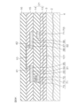
- the direction in which the notch 110 of the resistive layer 10 extends is referred to as a first direction, which is a direction along the main surface of the resistive layer 10 and perpendicular to the first direction (in this example In some cases, the X direction) is referred to as the second direction.
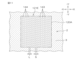
- a region of the first principal surface 3 of the semiconductor layer 2 that includes at least a region immediately below the resistive layer 10 (hereinafter referred to as the "irregularity forming region 120") has an uneven surface.
- a structure 121 is formed.
- the unevenness forming region 120 is set in a region directly below the resistance layer 10 on the first main surface 3 of the semiconductor layer 2 .
- the uneven structure 121 includes a plurality of grooves 122 extending parallel to the first direction (Y direction) at equal intervals in the second direction (X direction), and a convex portion 123 that is a portion between adjacent grooves 122. Contains.
- the width L of the groove 122 is preferably 0.2 nm or more and 1 ⁇ m or less.
- the interval S between the grooves 122 (width of the convex portion 123) is preferably 0.2 nm or more and 1 ⁇ m or less. It is preferable that the width L of the grooves 122 and the interval S between the grooves 122 be equal. That is, the width L of the grooves 122 and the interval S between the grooves 122 are preferably the same, and the width L of the grooves 122 and the interval S between the grooves 122 are preferably 0.2 nm or more and 1 ⁇ m or less. In this embodiment, the width L of the grooves 122 and the interval S between the grooves 122 are 0.5 ⁇ m.
- the depth of the groove 122 is preferably 100 nm or more and 300 nm or less, more preferably 150 nm or more and 300 nm or less. In this embodiment, the depth of groove 122 is 250 nm.
- an area wider than the area immediately below the resistance layer 10 on the first main surface 3 of the semiconductor layer 2 may be set as the unevenness forming area 120.
- a region on the first main surface 3 of the semiconductor layer 2 including a region immediately below the resistance layer 10 and a region in the vicinity thereof may be set as the unevenness forming region 120.
- a region of the first main surface 3 of the semiconductor layer 2 that belongs to the outer region 6 may be set as the unevenness forming region 120.
- 6A to 6S are cross-sectional views for explaining an example of a method for manufacturing the electronic component 1 shown in FIG. 1.
- 6A to 6S are cross-sectional views of portions corresponding to FIG. 2.
- a silicon wafer (not shown) is prepared as a source substrate for the semiconductor layer 2.
- a plurality of component formation areas corresponding to a plurality of electronic components 1 are arranged and set in a matrix on the surface of the silicon wafer.
- a boundary area (scribe line) is provided between adjacent component forming areas.
- the boundary region is a belt-shaped region having a substantially constant width, and is formed in a grid shape extending in two orthogonal directions. After performing the necessary steps on the silicon wafer, a plurality of electronic components 1 are obtained by cutting the silicon wafer along the boundary region.
- semiconductor layer (silicon wafer) 2 on which device region 6 and outer region 7 are formed is prepared. Then, a concave-convex structure 121 is formed in a concavo-convex formation region 120 including a region on the first main surface 3 of the semiconductor layer 2 that is to be directly under the resistive layer 10 .
- a mask (not shown) having a predetermined pattern is formed on the first main surface 3 of the semiconductor layer 2.
- the mask has a plurality of openings that expose regions in the first main surface 3 of the semiconductor layer 2 where the plurality of grooves 122 are to be formed.
- connection circuit formation layer 21 of the multilayer wiring structure 12 is formed on the first main surface 3 of the semiconductor layer 2.
- the connection circuit forming layer 21 includes a first insulating layer 13 , a second insulating layer 14 , one or more connection wiring layers 72 , and one or more connection via electrodes 73 .
- the first insulating layer 13 and the second insulating layer 14 are planarized by a CMP (Chemical Mechanical Polishing) method using an abrasive. A detailed description of the process of forming the connection circuit forming layer 21 will be omitted.
- CMP Chemical Mechanical Polishing
- a first base wiring layer 151 that becomes the base of the first lower wiring layer 31 and the second lower wiring layer 32 is formed on the connection circuit forming layer 21.
- the step of forming the first base wiring layer 151 includes a step of forming a first barrier layer 152, a main body layer 153, and a second barrier layer 154 in this order on the connection circuit forming layer 21.
- the step of forming the first barrier layer 152 includes the step of forming a Ti layer and a TiN layer in this order on the connection circuit forming layer 21.
- the Ti layer and the TiN layer may each be formed by sputtering.
- the step of forming the main body layer 153 includes the step of forming an AlCu alloy layer on the first barrier layer 152.
- the AlCu alloy layer may be formed by sputtering.
- the step of forming the second barrier layer 154 includes the step of forming a Ti layer and a TiN layer on the main body layer 153 in this order.
- the Ti layer and the TiN layer may each be formed by sputtering.
- a mask 155 having a predetermined pattern is formed on the first base wiring layer 151.
- the mask 155 has an opening 156 that covers the region of the first base wiring layer 151 where the first lower wiring layer 31 and the second lower wiring layer 32 are to be formed, and exposes the other region.
- first base wiring layer 151 is divided into the first lower wiring layer 31 and the second lower wiring layer 32.
- Mask 155 is then removed.
- the third insulating layer 15 covering the first lower wiring layer 31 and the second lower wiring layer 32 is formed on the connection circuit forming layer 21.
- the third insulating layer 15 may be formed by a CVD (Chemical Vapor Deposition) method.
- a first via hole 157 that exposes the first lower wiring layer 31 and a second via hole 158 that exposes the second lower wiring layer 32 are formed in the third insulating layer 15. .
- a mask 159 having a predetermined pattern is formed on the third insulating layer 15.
- the mask 159 has a plurality of openings 160 that expose regions in the third insulating layer 15 where the first via hole 157 and the second via hole 158 are to be formed.
- a base electrode layer 161 that becomes the base of the first via electrode 41 and the second via electrode 42 is formed on the third insulating layer 15.
- the step of forming the base electrode layer 161 includes the step of forming a barrier layer 162 and a main body layer 163 on the third insulating layer 15 in this order.
- the step of forming the barrier layer 162 includes the step of forming a Ti layer and a TiN layer on the third insulating layer 15 in this order.
- the Ti layer and the TiN layer may each be formed by sputtering.
- the process of forming body layer 163 includes forming a tungsten layer on barrier layer 162.
- the tungsten layer may be formed by CVD.
- a step of removing base electrode layer 161 is performed.
- Base electrode layer 161 is removed until third insulating layer 15 is exposed.
- the step of removing base electrode layer 161 may include a step of removing base electrode layer 161 by grinding.
- the grinding process of the base electrode layer 161 is performed by a CMP (Chemical Mechanical Polishing) method using an abrasive (abrasive).
- the step of grinding the base electrode layer 161 may include a step of planarizing the main surface of the third insulating layer 15.
- the first via electrode 41 is formed within the first via hole 157.
- a second via electrode 42 is formed within the second via hole 158.
- the polishing agent (abrasive grains) adhering to the main surface of third insulating layer 15 is removed by cleaning using a chemical solution.
- a part of the third insulating layer 15 is removed with a chemical solution together with the polishing agent (abrasive grains).
- Base resistance layer 164 that becomes the base of resistance layer 10 is formed on the main surface of third insulating layer 15.
- Base resistance layer 164 includes CrSi.
- Base resistance layer 164 may be formed by sputtering.
- the base resistance layer 164 (CrSi) is crystallized.
- the step of crystallizing the base resistance layer 164 includes annealing at a temperature and time such that the base resistance layer 164 (CrSi) is crystallized.
- the base resistance layer 164 may be heated at a temperature of 400° or more and 600° or less for 60 minutes or more and 120 minutes or less.
- a mask 166 having a predetermined pattern is formed on the base resistance layer 164.
- the mask 166 has an opening 167 that covers the region of the base resistance layer 164 where the resistance layer 10 is to be formed and exposes the other region.
- a fourth insulating layer 16 covering the resistance layer 10 is formed on the third insulating layer 15.
- the fourth insulating layer 16 may be formed by a CVD method.
- a first via hole 168 that exposes the first lower wiring layer 31 and a second via hole 169 that exposes the second lower wiring layer 32 are connected to the third insulating layer 15 and the fourth insulating layer. Formed in layer 16.
- a mask 170 having a predetermined pattern is formed on the fourth insulating layer 16.
- the mask 170 has a plurality of openings 171 that expose regions in the fourth insulating layer 16 where the first via hole 168 and the second via hole 169 are to be formed.
- a base electrode layer 172 that becomes the base of the first long via electrode 61 and the second long via electrode 62 is formed on the fourth insulating layer 16.
- the step of forming the base electrode layer 172 includes the step of forming a barrier layer 173 and a main body layer 174 on the fourth insulating layer 16 in this order.
- the step of forming the barrier layer 173 includes the step of forming a Ti layer and a TiN layer on the fourth insulating layer 16 in this order.
- the Ti layer and the TiN layer may each be formed by sputtering.
- the process of forming body layer 174 includes forming a tungsten layer on barrier layer 173.
- the tungsten layer may be formed by CVD.
- a step of removing base electrode layer 172 is performed.
- Base electrode layer 172 is removed until fourth insulating layer 16 is exposed.
- the step of removing base electrode layer 172 may include a step of removing base electrode layer 172 by grinding.
- the step of grinding the base electrode layer 172 is performed by a CMP method using an abrasive (abrasive).
- the step of grinding the base electrode layer 172 may include a step of planarizing the main surface of the fourth insulating layer 16.
- the first long via electrode 61 and the second long via electrode 62 are formed in the first via hole 168 and the second via hole 169, respectively.
- the polishing agent (abrasive grains) adhering to the main surface of the fourth insulating layer 16 may be removed by cleaning using a chemical solution.
- a portion of the fourth insulating layer 16 may be removed together with a polishing agent (abrasive grains) using a chemical solution.
- a second base wiring layer 175 that becomes the base of the first upper wiring layer 51 and the second upper wiring layer 52 is formed on the fourth insulating layer 16.
- the step of forming the second base wiring layer 175 includes a step of forming a first barrier layer 176, a main body layer 177, and a second barrier layer 178 in this order on the fourth insulating layer 16.
- the step of forming the first barrier layer 176 includes the step of forming a Ti layer and a TiN layer on the fourth insulating layer 16 in this order.
- the Ti layer and the TiN layer may each be formed by sputtering.
- the step of forming the main body layer 177 includes the step of forming an AlCu alloy layer on the first barrier layer 176.
- the AlCu alloy layer may be formed by sputtering.
- the step of forming the second barrier layer 178 includes the step of forming a Ti layer and a TiN layer on the main body layer 177 in this order.
- the Ti layer and the TiN layer may each be formed by sputtering.
- a mask 179 having a predetermined pattern is formed on the second base wiring layer 175.
- the mask 179 has an opening 180 in the outer region 7 that covers a region of the second base wiring layer 175 where the first upper wiring layer 51 and the second upper wiring layer 52 are to be formed, and exposes the other region. There is.
- the second base wiring layer 175 is divided into the first upper wiring layer 51 and the second upper wiring layer 52. Moreover, thereby, the multilayer wiring structure 12 including the connection circuit formation layer 21 and the resistance circuit formation layer 22 is formed on the first main surface 3 of the semiconductor layer 2. Mask 179 is then removed.
- a passivation layer 86 is formed on the multilayer wiring structure 12.
- Passivation layer 86 includes silicon nitride.
- Passivation layer 86 may be formed by a CVD method.
- the resin layer 87 is applied on top of the passivation layer 86.
- the resin layer 87 may contain polyimide as an example of a negative type photosensitive resin.
- resin layer 87 is selectively exposed and then developed. As a result, an opening 88 for laser trimming and a plurality of openings 181 that become the bases of the first pad opening 82 and the second pad opening 83 are formed in the resin layer 87.
- a notch 110 is formed in the resistance layer 10 by laser trimming.
- laser light is irradiated toward the resistance layer 10 from the opening 88 of the resin layer 87.
- a cut is made in the resistance layer 10.
- trimming is stopped.
- the electronic component 1 is manufactured through the steps including the above.
- a predetermined region including the region immediately below the resistance layer 10 on the first main surface 3 of the semiconductor layer 2
- An electronic component in which the uneven structure 121 is not formed will be referred to as a reference example.
- the first main surface of the semiconductor layer 2 is formed to be a flat surface over the entire area.
- the laser incident light and the reflected light reflected from the first main surface 3 of the semiconductor layer 2 interfere.
- locations with high electric field strength and locations with low electric field strength appear alternately in the thickness direction.
- the height position where the electric field strength is high and the height position where the electric field strength is low are determined by the wavelength of the laser light and the material (refractive index) of the member constituting the multilayer wiring structure 12.
- the resistance layer 10 In order to form the notch 110 in the resistance layer 10, the resistance layer 10 needs to be placed at a position in the thickness direction in the multilayer wiring structure 12 where the electric field strength is high. However, since there are variations in the film thickness of the insulating layer (lower insulating layer) between the semiconductor layer 2 and the resistance layer 10 within the wafer plane, the resistance layer 10 and the semiconductor layer 2 in each component forming area vary. There is variation in the distance between. As a result, among the plurality of component formation regions on the wafer surface, the resistance layer 10 is disposed at a position where the electric field strength is low, and it becomes impossible to form the notch 110 in the resistance layer 10 in some parts.
- a concave-convex structure 121 is formed in a concavo-convex formation region 120 including a region immediately below the resistive layer 10 on the first main surface 3 of the semiconductor layer 2 .
- the uneven structure 121 includes a plurality of grooves 122 extending parallel to the first direction (Y direction) at equal intervals in the second direction (X direction), and a convex portion 123 that is a portion between two adjacent grooves 122. including.
- a plurality of samples corresponding to a plurality of types of resistor components having a structure substantially similar to that shown in FIG. 2 but having different uneven structures in the uneven formation region 120 were prepared.
- the resistance layer 10 used had a length in the X direction and a length in the Y direction of 50 ⁇ m.
- the region immediately below the resistance layer 10 on the first main surface 3 of the semiconductor layer 2 was set as the unevenness forming region 120A.
- a sample corresponding to one type of resistor component was created by preparing a wafer having multiple component forming areas and creating the corresponding type of resistor component in each component forming area. Specifically, the following 1st to 13th samples were prepared.
- the uneven structure 121A consists of one recess 130 formed in the uneven formation region 120A.
- the planar area of the recess 130 is approximately equal to the planar area of the unevenness forming region 120A.
- the depth of the recess 130 is 250 nm.
- the uneven structure 121B has a plurality of first grooves 131 extending parallel to the X direction at equal intervals in the Y direction, and a Y groove at equal intervals in the X direction. It has a plurality of second grooves 132 that extend parallel to the direction, and a plurality of convex portions 133 that are square in plan view and surrounded by the first groove 131 and the second groove 132. The interval between two adjacent first grooves 131 and the interval between two adjacent second grooves 132 are equal. The depth of the first groove 131 and the second groove 132 is 250 nm.
- the differences between the second to seventh samples are as follows.
- Second sample In plan view, the length of one side of the convex portion 133 is 1 ⁇ m, and the ratio of the total area of the upper surface of the convex portion 133 to the entire unevenness forming region 80 is 75%.
- the length of one side of the convex portion 133 is 1 ⁇ m, and the ratio of the total area of the upper surface of the convex portion 133 to the entire unevenness forming region 80 is 50%.
- the length of one side of the convex portion 133 is 1 ⁇ m, and the ratio of the total area of the upper surface of the convex portion 133 to the entire unevenness forming region 80 is 25%.
- the length of one side of the convex portion 133 is 0.5 ⁇ m, and the ratio of the total area of the upper surface of the convex portion 133 to the entire unevenness forming region 80 is 50%.
- the length of one side of the convex portion 133 is 0.5 ⁇ m, and the ratio of the total area of the upper surface of the convex portion 133 to the entire unevenness forming region 80 is 25%.
- the length of one side of the convex portion 133 is 0.35 ⁇ m, and the ratio of the total area of the upper surface of the convex portion 133 to the entire unevenness forming region 80 is 37%.
- the unevenness 121C has a plurality of first grooves 134 extending parallel to the X direction at equal intervals in the Y direction, and a plurality of first grooves 134 extending in the Y direction at equal intervals in the X direction. It has a plurality of second grooves 135 that extend in parallel to , and a plurality of convex portions 136 that are circular in plan view and surrounded by the first grooves 134 and the second grooves 135 . The distance between two adjacent first grooves 134 and the distance between two adjacent second grooves 135 are equal. The plurality of convex portions 136 are arranged at equal intervals in the X direction and the Y direction. The depth of the first groove 134 and the second groove 135 is 250 nm. The differences between the 8th and 9th samples are as follows.
- the diameter of the convex portion 136 is 1 ⁇ m, and the interval between two convex portions 136 adjacent to each other in the X direction (the distance between two convex portions 136 adjacent to each other in the Y direction) is 0.5 ⁇ m. be.
- the diameter of the convex portion 136 is 1 ⁇ m, and the interval between two convex portions 136 adjacent to each other in the X direction (the distance between two convex portions 136 adjacent to each other in the Y direction) is 0.26 ⁇ m. be.
- the uneven structure 121D includes a plurality of grooves 141 extending parallel to the second direction (X direction) at equal intervals in the first direction (Y direction), It consists of a convex portion 142 that is a portion between two adjacent grooves 141.
- the depth of the groove 141 is 250 nm.
- Width L of groove 141 and interval S between grooves 141 are 1 ⁇ m.
- Width L of groove 141 and interval S between grooves 141 are 0.5 ⁇ m.
- the uneven structure 121E is arranged in the first direction (Y direction) at equal intervals in the second direction (X direction). It consists of a plurality of grooves 143 extending parallel to the , and a convex portion 144 that is a portion between two adjacent grooves 143 . The depth of the groove 143 is 250 nm.
- the differences between the 12th and 13th samples are as follows.
- Width L of groove 143 and interval S of groove 143 are 1 ⁇ m.
- Width L of groove 143 and interval S between grooves 143 are 0.5 ⁇ m.
- a laser beam is irradiated perpendicularly to the central length of the main surface of the resistive layer 10 in the second direction (X direction) for each of the plurality of resistive components selected in advance for each sample, and the laser beam is directed in the first direction. (Y direction). Then, it was determined whether the resistance layer 10 could be cut based on whether the resistance value changed.
- the wavelength of the laser light is 1064 nm.
- the resistance layer 10 could not be cut in all 20 samples (20NG/20).
- the resistance layer 10 could not be cut in three out of six samples (3NG/6).
- the resistance layer 10 could not be cut in 6 out of 6 samples (6NG/6).
- the resistance layer 10 could not be cut in 5 out of 6 samples (5NG/6).
- the resistance layer 10 could not be cut in 5 out of 6 samples (5NG/6).
- the resistance layer 10 could not be cut in 11 out of 20 samples (11NG/20).
- the resistance layer 10 could not be cut in one of the 20 samples (1NG/20).
- the 12th sample and the 13th sample have a lower ratio of resistive components for which the resistive layer 10 cannot be cut compared to the number of components to be inspected compared to the other first to eleventh samples.
- the cutting direction of the resistance layer 10 is the first direction (Y direction)
- the direction along the main surface of the resistance layer 10 and orthogonal to the first direction is the second direction (X direction)
- the unevenness is formed.
Landscapes
- Engineering & Computer Science (AREA)
- Power Engineering (AREA)
- Physics & Mathematics (AREA)
- Condensed Matter Physics & Semiconductors (AREA)
- General Physics & Mathematics (AREA)
- Computer Hardware Design (AREA)
- Microelectronics & Electronic Packaging (AREA)
- Manufacturing & Machinery (AREA)
- Semiconductor Integrated Circuits (AREA)
Abstract
Un composant électronique selon la présente invention comprend : une couche semi-conductrice ayant une première surface principale et une seconde surface principale qui est sur le côté inverse de la première surface principale ; une couche isolante inférieure formée sur la première surface principale de la couche semi-conductrice ; une couche de résistance qui est formée sur la couche isolante inférieure et qui a une section d'encoche s'étendant dans une première direction prescrite à partir d'une partie de la périphérie de la couche de résistance ; une couche isolante supérieure formée sur la couche isolante inférieure de façon à recouvrir la couche de résistance ; et une structure d'aspérité formée dans une région prescrite sur la première surface principale de la couche semi-conductrice, ladite région prescrite comprenant au moins une région directement au-dessous de la couche de résistance. La structure d'aspérité comprend : une pluralité de rainures qui sont agencées à des intervalles égaux dans une seconde direction, qui est une direction le long de la première surface principale et est orthogonale à la première direction, et qui s'étendent parallèlement à la première direction ; et des saillies dont chacune est une partie entre deux rainures voisines.
Applications Claiming Priority (2)
| Application Number | Priority Date | Filing Date | Title |
|---|---|---|---|
| JP2022052630 | 2022-03-28 | ||
| JP2022-052630 | 2022-03-28 |
Publications (1)
| Publication Number | Publication Date |
|---|---|
| WO2023189109A1 true WO2023189109A1 (fr) | 2023-10-05 |
Family
ID=88200602
Family Applications (1)
| Application Number | Title | Priority Date | Filing Date |
|---|---|---|---|
| PCT/JP2023/007288 WO2023189109A1 (fr) | 2022-03-28 | 2023-02-28 | Composant électronique et son procédé de production |
Country Status (1)
| Country | Link |
|---|---|
| WO (1) | WO2023189109A1 (fr) |
Citations (3)
| Publication number | Priority date | Publication date | Assignee | Title |
|---|---|---|---|---|
| JPH1022452A (ja) * | 1996-07-02 | 1998-01-23 | Denso Corp | 半導体装置およびその製造方法 |
| JPH10144866A (ja) * | 1996-11-06 | 1998-05-29 | Denso Corp | 半導体装置およびその製造方法 |
| JP2020155604A (ja) * | 2019-03-20 | 2020-09-24 | ローム株式会社 | 電子部品 |
-
2023
- 2023-02-28 WO PCT/JP2023/007288 patent/WO2023189109A1/fr unknown
Patent Citations (3)
| Publication number | Priority date | Publication date | Assignee | Title |
|---|---|---|---|---|
| JPH1022452A (ja) * | 1996-07-02 | 1998-01-23 | Denso Corp | 半導体装置およびその製造方法 |
| JPH10144866A (ja) * | 1996-11-06 | 1998-05-29 | Denso Corp | 半導体装置およびその製造方法 |
| JP2020155604A (ja) * | 2019-03-20 | 2020-09-24 | ローム株式会社 | 電子部品 |
Similar Documents
| Publication | Publication Date | Title |
|---|---|---|
| US20190244763A1 (en) | Chip capacitor and method for manufacturing the same | |
| US6534374B2 (en) | Single damascene method for RF IC passive component integration in copper interconnect process | |
| US8048763B2 (en) | Semiconductor device manufacturing method | |
| KR100709775B1 (ko) | 반도체 소자 및 그 제조 방법 | |
| US20150162396A1 (en) | Semiconductor device and method for manufacturing semiconductor device | |
| JP2017212299A (ja) | 半導体装置およびその製造方法 | |
| US11637100B2 (en) | Semiconductor device having capacitor and resistor and a method of forming the same | |
| US20110318900A1 (en) | Semiconductor device and method of manufacturing the same | |
| WO2023189109A1 (fr) | Composant électronique et son procédé de production | |
| JP7340948B2 (ja) | 電子部品 | |
| US11189685B2 (en) | Resistance element and manufacturing method of resistance element | |
| US7298020B2 (en) | Semiconductor device and method of manufacturing the same | |
| US20220302028A1 (en) | Electronic component | |
| US20210305157A1 (en) | Electronic component | |
| US20230343578A1 (en) | Semiconductor device manufacturing method and wafer structural object | |
| US8022525B2 (en) | Semiconductor device and method of manufacturing semiconductor device | |
| JP6655469B2 (ja) | 半導体装置およびその製造方法 | |
| JP7232679B2 (ja) | 電子部品 | |
| JP7440212B2 (ja) | 薄膜抵抗およびその製造方法、ならびに、薄膜抵抗を備えた電子部品 | |
| US11408925B2 (en) | Semiconductor element and method for identifying semiconductor element | |
| KR100854925B1 (ko) | 반도체 소자 및 그 제조방법 | |
| WO2021177071A1 (fr) | Composant électronique | |
| KR100221688B1 (ko) | 반도체 장치 및 그의 제조 방법 | |
| CN117096138A (zh) | 半导体装置 | |
| TW202301557A (zh) | 半導體元件 |
Legal Events
| Date | Code | Title | Description |
|---|---|---|---|
| 121 | Ep: the epo has been informed by wipo that ep was designated in this application |
Ref document number: 23779139 Country of ref document: EP Kind code of ref document: A1 |