WO2023188756A1 - 半導体装置 - Google Patents
半導体装置 Download PDFInfo
- Publication number
- WO2023188756A1 WO2023188756A1 PCT/JP2023/002430 JP2023002430W WO2023188756A1 WO 2023188756 A1 WO2023188756 A1 WO 2023188756A1 JP 2023002430 W JP2023002430 W JP 2023002430W WO 2023188756 A1 WO2023188756 A1 WO 2023188756A1
- Authority
- WO
- WIPO (PCT)
- Prior art keywords
- gate
- gate electrode
- conductive part
- semiconductor device
- conductive
- Prior art date
- Legal status (The legal status is an assumption and is not a legal conclusion. Google has not performed a legal analysis and makes no representation as to the accuracy of the status listed.)
- Ceased
Links
Images




Classifications
-
- H—ELECTRICITY
- H10—SEMICONDUCTOR DEVICES; ELECTRIC SOLID-STATE DEVICES NOT OTHERWISE PROVIDED FOR
- H10D—INORGANIC ELECTRIC SEMICONDUCTOR DEVICES
- H10D30/00—Field-effect transistors [FET]
- H10D30/60—Insulated-gate field-effect transistors [IGFET]
- H10D30/64—Double-diffused metal-oxide semiconductor [DMOS] FETs
- H10D30/66—Vertical DMOS [VDMOS] FETs
- H10D30/668—Vertical DMOS [VDMOS] FETs having trench gate electrodes, e.g. UMOS transistors
-
- H—ELECTRICITY
- H10—SEMICONDUCTOR DEVICES; ELECTRIC SOLID-STATE DEVICES NOT OTHERWISE PROVIDED FOR
- H10D—INORGANIC ELECTRIC SEMICONDUCTOR DEVICES
- H10D62/00—Semiconductor bodies, or regions thereof, of devices having potential barriers
- H10D62/10—Shapes, relative sizes or dispositions of the regions of the semiconductor bodies; Shapes of the semiconductor bodies
- H10D62/124—Shapes, relative sizes or dispositions of the regions of semiconductor bodies or of junctions between the regions
- H10D62/126—Top-view geometrical layouts of the regions or the junctions
- H10D62/127—Top-view geometrical layouts of the regions or the junctions of cellular field-effect devices, e.g. multicellular DMOS transistors or IGBTs
-
- H—ELECTRICITY
- H10—SEMICONDUCTOR DEVICES; ELECTRIC SOLID-STATE DEVICES NOT OTHERWISE PROVIDED FOR
- H10D—INORGANIC ELECTRIC SEMICONDUCTOR DEVICES
- H10D64/00—Electrodes of devices having potential barriers
- H10D64/111—Field plates
- H10D64/117—Recessed field plates, e.g. trench field plates or buried field plates
-
- H—ELECTRICITY
- H10—SEMICONDUCTOR DEVICES; ELECTRIC SOLID-STATE DEVICES NOT OTHERWISE PROVIDED FOR
- H10D—INORGANIC ELECTRIC SEMICONDUCTOR DEVICES
- H10D64/00—Electrodes of devices having potential barriers
- H10D64/60—Electrodes characterised by their materials
- H10D64/66—Electrodes having a conductor capacitively coupled to a semiconductor by an insulator, e.g. MIS electrodes
- H10D64/661—Electrodes having a conductor capacitively coupled to a semiconductor by an insulator, e.g. MIS electrodes the conductor comprising a layer of silicon contacting the insulator, e.g. polysilicon having vertical doping variation
- H10D64/662—Electrodes having a conductor capacitively coupled to a semiconductor by an insulator, e.g. MIS electrodes the conductor comprising a layer of silicon contacting the insulator, e.g. polysilicon having vertical doping variation the conductor further comprising additional layers, e.g. multiple silicon layers having different crystal structures
-
- H—ELECTRICITY
- H10—SEMICONDUCTOR DEVICES; ELECTRIC SOLID-STATE DEVICES NOT OTHERWISE PROVIDED FOR
- H10D—INORGANIC ELECTRIC SEMICONDUCTOR DEVICES
- H10D64/00—Electrodes of devices having potential barriers
- H10D64/20—Electrodes characterised by their shapes, relative sizes or dispositions
- H10D64/23—Electrodes carrying the current to be rectified, amplified, oscillated or switched, e.g. sources, drains, anodes or cathodes
- H10D64/251—Source or drain electrodes for field-effect devices
- H10D64/252—Source or drain electrodes for field-effect devices for vertical or pseudo-vertical devices
- H10D64/2527—Source or drain electrodes for field-effect devices for vertical or pseudo-vertical devices for vertical devices wherein the source or drain electrodes are recessed in semiconductor bodies
-
- H—ELECTRICITY
- H10—SEMICONDUCTOR DEVICES; ELECTRIC SOLID-STATE DEVICES NOT OTHERWISE PROVIDED FOR
- H10D—INORGANIC ELECTRIC SEMICONDUCTOR DEVICES
- H10D64/00—Electrodes of devices having potential barriers
- H10D64/20—Electrodes characterised by their shapes, relative sizes or dispositions
- H10D64/27—Electrodes not carrying the current to be rectified, amplified, oscillated or switched, e.g. gates
- H10D64/311—Gate electrodes for field-effect devices
- H10D64/411—Gate electrodes for field-effect devices for FETs
- H10D64/511—Gate electrodes for field-effect devices for FETs for IGFETs
- H10D64/512—Disposition of the gate electrodes, e.g. buried gates
- H10D64/513—Disposition of the gate electrodes, e.g. buried gates within recesses in the substrate, e.g. trench gates, groove gates or buried gates
Definitions
- the present disclosure relates to a semiconductor device.
- Patent Document 1 A MISFET having a trench gate structure including a gate trench, an insulating layer, a bottom electrode, and an opening electrode is known (see, for example, Patent Document 1).
- Patent Document 1 discloses that the opening side electrode functions as a gate electrode and contains conductive polysilicon.
- a semiconductor device includes a semiconductor layer, a trench formed in the semiconductor layer and including sidewalls, an insulating layer formed on the semiconductor layer, and a gate electrode disposed in the trench. It is equipped with The insulating layer includes a gate insulating portion interposed between the semiconductor layer and the gate electrode and covering the sidewall of the trench.
- the gate electrode includes a first conductive part in contact with the gate insulating part and a second conductive part including a side surface in contact with the first conductive part, the first conductive part being made of polysilicon, and the first conductive part being in contact with the first conductive part.
- the second conductive part is made of metal.
- gate resistance can be reduced while suppressing changes in gate threshold voltage.
- FIG. 1 is a schematic plan view of an exemplary semiconductor device according to a first embodiment.
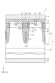
- FIG. 2 is a schematic cross-sectional view of the gate trench taken along line F2-F2 in FIG.
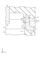
- FIG. 3 is a partially enlarged view of FIG. 2.
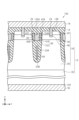
- FIG. 4 is a schematic cross-sectional view of the gate trench taken along line F4-F4 in FIG.
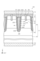
- FIG. 5 is a schematic cross-sectional view of an exemplary semiconductor device according to the second embodiment.
- FIG. 6 is a schematic cross-sectional view of an exemplary semiconductor device according to the third embodiment.
- FIG. 7 is a schematic cross-sectional view showing a modified example of the gate electrode.
- FIG. 8 is a schematic cross-sectional view showing a modified example of the gate contact.
- FIG. 1 is a schematic plan view of an exemplary semiconductor device 10 according to a first embodiment.
- planar view used in the present disclosure refers to viewing the semiconductor device 10 in the Z-axis direction of the mutually orthogonal XYZ axes shown in FIG. Unless explicitly stated otherwise, “planar view” refers to viewing the semiconductor device 10 from above along the Z-axis.
- the semiconductor device 10 is, for example, a metal-insulator-semiconductor field effect transistor (MISFET) having a trench gate structure.
- Semiconductor device 10 includes a semiconductor layer 12 and an insulating layer 14 formed on semiconductor layer 12.
- the semiconductor layer 12 can be formed from silicon (Si), for example.
- the semiconductor layer 12 includes a first surface 12A, which will be described later with reference to FIG. 2, and a second surface 12B opposite to the first surface 12A.
- the Z-axis direction may be a direction perpendicular to the first surface 12A and the second surface 12B of the semiconductor layer 12. Since the semiconductor layer 12 is covered with the insulating layer 14, only the rectangular outer edge of the semiconductor layer 12 is shown in FIG.
- the insulating layer 14 can be formed from a silicon oxide film (SiO 2 ), for example. Insulating layer 14 may additionally or alternatively include a layer formed from an insulating material different from SiO2 , such as silicon nitride (SiN).
- the semiconductor device 10 may further include a gate wiring 16 formed on the insulating layer 14 and a source wiring 18 formed on the insulating layer 14.
- the source wiring 18 is separated from the gate wiring 16.
- the gate wiring 16 and the source wiring 18 are made of at least one of titanium (Ti), nickel (Ni), gold (Au), silver (Ag), copper (Cu), aluminum (Al), a copper alloy, and an aluminum alloy. It can be formed from one.
- the gate wiring 16 can generally extend along the outer edge of the semiconductor layer 12.
- the gate wiring 16 includes a first gate wiring part 16X1 and a second gate wiring part 16X2 extending in the X-axis direction, and a third gate wiring part 16Y1 and a fourth gate wiring part 16Y2 extending in the Y-axis direction. including.
- the first gate wiring section 16X1 is connected between one end of the third gate wiring section 16Y1 and one end of the fourth gate wiring section 16Y2.
- the second gate wiring section 16X2 is connected to the other end of the third gate wiring section 16Y1, but is not connected to the other end of the fourth gate wiring section 16Y2.
- the gate wiring 16 may further include a gate pad portion 16P. In the example of FIG. 1, the other end of the fourth gate wiring section 16Y2 is connected to the gate pad section 16P.
- the source wiring 18 may include an inner source wiring part 18a that is at least partially surrounded by the gate wiring 16, and an outer source wiring part 18b that surrounds the gate wiring 16. Further, the source wiring 18 can further include a source connection part 18c that connects the inner source wiring part 18a and the outer source wiring part 18b.
- the gate wiring 16 forms an open loop that partially surrounds the inner source wiring portion 18a.
- the source connecting portion 18c is arranged at a location where the loop of the gate wiring 16 is open, so that the inner source wiring portion 18a can be connected to the outer source wiring portion 18b.
- the source connection portion 18c passes between the second gate wiring portion 16X2 and the gate pad portion 16P.
- the loop of the gate wiring 16 may be opened at different locations.
- the gate wiring 16 may form a closed loop in plan view.
- the semiconductor device 10 further includes a gate trench 20 (also simply referred to as trench 20) formed in the semiconductor layer 12.
- the gate trench 20 can be arranged so as to at least partially overlap both the gate wiring 16 and the source wiring 18 in a plan view.
- the semiconductor device 10 may include a plurality of gate trenches 20, and some of the plurality of gate trenches 20 may be aligned parallel to each other at equal intervals.
- the gate trench 20 extends in the X-axis direction and is arranged to intersect with the third gate interconnection section 16Y1 or the fourth gate interconnection section 16Y2 in plan view.
- the semiconductor device 10 may further include a gate contact plug 22 and a source contact plug 24 that penetrate the insulating layer 14.
- Gate contact plug 22 is coupled to gate wiring 16 .
- the gate contact plug 22 can be placed in a region where the gate trench 20 and the gate wiring 16 intersect in plan view.
- Source contact plug 24 is coupled to source wiring 18 .
- the source contact plug 24 extends parallel to the gate trenches 20 and can be placed between the two gate trenches 20 .
- the semiconductor device 10 may further include a termination trench 26 formed in the semiconductor layer 12.
- the termination trench 26 includes a first termination trench portion 26X1 and a second termination trench portion 26X2 extending in the X-axis direction, and a third termination trench portion 26Y1 and a fourth termination trench portion 26Y2 extending in the Y-axis direction.
- the plurality of gate trenches 20 aligned parallel to each other are arranged between the first termination trench portion 26X1 and the second termination trench portion 26X2 in plan view.
- the third termination trench portion 26Y1 overlaps with the inner source wiring portion 18a in plan view.
- the fourth termination trench portion 26Y2 overlaps with the outer source wiring portion 18b in plan view.
- the gate trench 20 extends between and communicates with the third termination trench portion 26Y1 and the fourth termination trench portion 26Y2. Therefore, the gate trench 20 overlaps both the inner source wiring part 18a and the outer source wiring part 18b in plan view.
- the semiconductor device 10 may further include a first field plate contact plug 28 and a second field plate contact plug 30 that penetrate the insulating layer 14.
- the first field plate contact plug 28 is coupled to the inner source wiring portion 18a.
- the first field plate contact plug 28 overlaps the third end trench portion 26Y1 in plan view.
- the second field plate contact plug 30 is coupled to the outer source wiring portion 18b.
- the second field plate contact plug 30 overlaps with the fourth end trench portion 26Y2 in plan view.
- Each of the gate contact plug 22, source contact plug 24, first field plate contact plug 28, and second field plate contact plug 30 can be formed from any metal material.
- each contact plug 22, 24, 28, 30 may be formed from at least one of tungsten (W), titanium (Ti), and titanium nitride (TiN).
- semiconductor device 10 may not include termination trench 26.
- field plate contact plugs 28 and 30 may be arranged to overlap the ends of each gate trench 20.
- the semiconductor device 10 may further include a gate trench 20 extending in the Y-axis direction, and the first gate wiring part 16X1 and the second gate wiring part 16X2 intersect with the gate trench 20 extending in the Y-axis direction. It's okay.
- the semiconductor device 10 may not include the source wiring 18.
- the field plate contact plug 30 may be arranged to overlap the end of each gate trench 20.
- FIG. 2 is a schematic cross-sectional view of the semiconductor device 10 of FIG. 1 taken along line F2-F2.
- the semiconductor layer 12 may include a semiconductor substrate 32 and an epitaxial layer 34 formed on the semiconductor substrate 32.
- the semiconductor substrate 32 includes the first surface 12A of the semiconductor layer 12, and the epitaxial layer 34 includes the second surface 12B of the semiconductor layer 12.
- the semiconductor substrate 32 may be a Si substrate, for example.
- the semiconductor substrate 32 corresponds to the drain region of the MISFET.
- the epitaxial layer 34 may be a Si layer epitaxially grown on a Si substrate.
- Epitaxial layer 34 can include a drift region 36 , a body region 38 formed on drift region 36 , and a source region 40 formed on body region 38 .
- Source region 40 may include second surface 12B of semiconductor layer 12.
- the drain region (semiconductor substrate 32) may be an n-type region containing n-type impurities.
- the n-type impurity concentration of the drain region (semiconductor substrate 32) can be set to 1 ⁇ 10 18 cm ⁇ 3 or more and 1 ⁇ 10 20 cm ⁇ 3 or less.
- the drain region (semiconductor substrate 32) may have a thickness of 50 ⁇ m or more and 450 ⁇ m or less.
- the drift region 36 may be an n-type region containing n-type impurities at a lower concentration than the drain region (semiconductor substrate 32).
- the n-type impurity concentration of the drift region 36 can be set to 1 ⁇ 10 15 cm ⁇ 3 or more and 1 ⁇ 10 18 cm ⁇ 3 or less.
- the drift region 36 may have a thickness of 1 ⁇ m or more and 25 ⁇ m or less.
- Body region 38 may be a p-type region containing p-type impurities.
- the p-type impurity concentration of the body region 38 can be set to 1 ⁇ 10 16 cm ⁇ 3 or more and 1 ⁇ 10 18 cm ⁇ 3 or less.
- Body region 38 may have a thickness of 0.2 ⁇ m or more and 1.0 ⁇ m or less.
- Source region 40 may be an n-type region containing a higher concentration of n-type impurities than drift region 36 .
- the n-type impurity concentration of the source region 40 can be set to 1 ⁇ 10 19 cm ⁇ 3 or more and 1 ⁇ 10 21 cm ⁇ 3 or less.
- the source region 40 may have a thickness of 0.1 ⁇ m or more and 1 ⁇ m or less.
- the n-type is also referred to as a first conductivity type, and the p-type is also referred to as a second conductivity type.
- the n-type impurity may be, for example, phosphorus (P) or arsenic (As).
- the p-type impurity may be, for example, boron (B), aluminum (Al), or the like.
- the gate trench 20 has an opening in the second surface 12B of the semiconductor layer 12 and has a depth in the Z-axis direction. Gate trench 20 extends through source region 40 and body region 38 of semiconductor layer 12 to drift region 36 . Gate trench 20 has sidewalls 20A and a bottom wall 20B, and bottom wall 20B is adjacent to drift region 36. The depth of the gate trench 20 may be 1 ⁇ m or more and 10 ⁇ m or less.
- the sidewall 20A of the gate trench 20 may extend in a direction perpendicular to the second surface 12B of the semiconductor layer 12 (Z-axis direction), or may be inclined with respect to the Z-axis direction. In one example, the sidewall 20A may be inclined with respect to the Z-axis direction so that the width of the gate trench 20 becomes smaller toward the bottom wall 20B. Further, the bottom wall 20B of the gate trench 20 does not necessarily have to be flat, and may be partially or entirely curved, for example.
- the semiconductor device 10 further includes a gate electrode 42 and a field plate electrode 44 arranged within the gate trench 20.
- the gate electrode 42 may be an electrode configured to be applied with a gate voltage
- the field plate electrode 44 may be an electrode configured to be applied with a reference voltage (or source voltage).
- the gate electrode 42 includes a top surface 42A covered with the insulating layer 14 and a bottom surface 42B opposite to the top surface 42A.
- Field plate electrode 44 is arranged below gate electrode 42 within gate trench 20 . More specifically, the field plate electrode 44 is arranged between the bottom surface 42B of the gate electrode 42 and the bottom wall 20B of the gate trench 20. At least a portion of the bottom surface 42B of the gate electrode 42 faces the field plate electrode 44 with the insulating layer 14 in between.
- the gate electrode 42 further includes a side surface 42C that faces the side wall 20A of the gate trench 20.
- the upper surface 42A of the gate electrode 42 can be located below the second surface 12B of the semiconductor layer 12. Further, the bottom surface 42B of the gate electrode 42 is located near the interface between the drift region 36 and the body region 38 in the Z-axis direction, and preferably may be located below the interface.
- the top surface 42A and bottom surface 42B of the gate electrode 42 may be flat or curved.
- the gate electrode 42 and the field plate electrode 44 are surrounded by the insulating layer 14.
- Field plate electrode 44 may have a smaller width than gate electrode 42 . Due to the relatively small width of field plate electrode 44, the thickness of insulating layer 14 surrounding field plate electrode 44 is relatively large. Thereby, electric field concentration within the gate trench 20 can be alleviated.
- the insulating layer 14 includes a gate insulating portion 46 interposed between the gate electrode 42 and the semiconductor layer 12 and covering the side wall 20A of the gate trench 20.
- the gate insulating portion 46 is a part of the insulating layer 14 between the side surface 42C of the gate electrode 42 and the side wall 20A of the gate trench 20.
- the gate insulating portion 46 is in contact with both the side surface 42C of the gate electrode 42 and the side wall 20A of the gate trench 20. That is, the gate electrode 42 faces the semiconductor layer 12 with the gate insulating section 46 interposed therebetween.
- a predetermined voltage is applied to the gate electrode 42, a channel is formed in the p-type body region 38 adjacent to the gate insulating portion 46.
- the semiconductor device 10 can control the flow of electrons in the Z-axis direction between the n-type source region 40 and the n-type drift region 36 via this channel.
- Semiconductor layer 12 may further include contact region 48 .
- Contact region 48 may be a p-type region containing p-type impurities.
- the p-type impurity concentration of the contact region 48 is higher than that of the body region 38, and can be set to 1 ⁇ 10 19 cm ⁇ 3 or more and 1 ⁇ 10 21 cm ⁇ 3 or less.
- Source contact plug 24 extends through insulating layer 14 and source region 40 to contact contact region 48 . The source contact plug 24 can electrically connect the source wiring 18 formed on the insulating layer 14 to the contact region 48 of the semiconductor layer 12.
- the semiconductor device 10 may further include a drain electrode 50 formed on the first surface 12A of the semiconductor layer 12.
- the drain electrode 50 is adjacent to and electrically connected to the drain region (semiconductor substrate 32).
- Drain electrode 50 is formed from at least one of titanium (Ti), nickel (Ni), gold (Au), silver (Ag), copper (Cu), aluminum (Al), copper alloy, and aluminum alloy. be able to.
- the gate electrode 42 includes a first conductive part 52 and a second conductive part 54 including a side surface 54A in contact with the first conductive part 52.
- the second conductive part 54 may be embedded in a recess 52A formed in the first conductive part 52.
- the first conductive portion 52 includes a side surface 42C and a bottom surface 42B of the gate electrode 42.
- a portion of the upper surface 42A of the gate electrode 42 is included in the second conductive part 54, and the rest of the upper surface 42A of the gate electrode 42 is included in the first conductive part 52.
- the first conductive part 52 is in contact with the gate insulating part 46. More specifically, the first conductive portion 52 is in contact with the gate insulating portion 46 via the side surface 42C of the gate electrode 42. Therefore, the first conductive portion 52 faces the body region 38 of the semiconductor layer 12 with the gate insulating portion 46 interposed therebetween.
- the first conductive part 52 is made of polysilicon
- the second conductive part 54 is made of metal.
- the second conductive portion 54 may be made of a metal containing at least one of tungsten (W), titanium (Ti), titanium nitride (TiN), and nickel (Ni).
- the second conductive portion 54 may include titanium nitride as a barrier metal and tungsten as an embedded metal.
- titanium nitride may be formed along the recess 52A of the first conductive portion 52, and tungsten may be embedded on the titanium nitride. By forming titanium nitride along the recessed portion 52A, diffusion of tungsten into the first conductive portion 52 (polysilicon) can be suppressed.
- the second conductive part 54 has a resistivity lower than that of the first conductive part 52.
- polysilicon may be doped with impurities.
- the field plate electrode 44 can be formed from polysilicon. In another example, field plate electrode 44 may be formed from metal. In that case, the field plate electrode 44 may be formed from the same metal as the second conductive portion 54.
- FIG. 3 is a partially enlarged view of FIG. 2.
- the thickness of the first conductive part 52 between the bottom surface 42B of the gate electrode 42 and the second conductive part 54 is T1
- the thickness of the first conductive part 52 between the bottom surface 42B of the gate electrode 42 and the second conductive part 54 is T1.
- the thickness of the first conductive portion 52 is assumed to be T2.
- the thickness T1 corresponds to the distance between the bottom surface 42B of the gate electrode 42 and the second conductive portion 54. Note that the thickness T1 is a dimension in the Z-axis direction.
- the thickness T2 corresponds to the distance between the side surface 42C of the gate electrode 42 and the second conductive portion 54 (side surface 54A). Note that the thickness T2 is a dimension in a direction perpendicular to the side surface 42C.
- the thickness T1 is also referred to as the bottom thickness T1 of the first conductive part 52, and the thickness T2 is also referred to as the side thickness T2 of the first conductive part 52.
- the thickness of the gate insulating portion 46 is assumed to be T3.
- Thickness T3 corresponds to the distance between side wall 20A of gate trench 20 and side surface 42C of gate electrode 42. Note that the thickness T3 is a dimension in a direction perpendicular to the side wall 20A.
- the bottom thickness T1 of the first conductive part 52 may be the same as the side thickness T2 of the first conductive part 52. More preferably, the bottom thickness T1 of the first conductive part 52 may be smaller than the side thickness T2 of the first conductive part 52. Since the first conductive part 52 made of polysilicon has a higher resistivity than the second conductive part 54 made of metal, the smaller the bottom thickness T1 of the first conductive part 52 is, the more Gate resistance of the semiconductor device 10 can be reduced. Therefore, the bottom thickness T1 of the first conductive portion 52 may be made as small as possible. For example, the bottom thickness T1 of the first conductive portion 52 may be less than or equal to the thickness T3 of the gate insulating portion 46.
- the gate resistance of the semiconductor device 10 can be further reduced.
- the side thickness T2 of the first conductive portion 52 can be set in consideration of both the gate resistance and the gate threshold voltage.
- the side thickness T2 of the first conductive portion 52 may be greater than the thickness T3 of the gate insulating portion 46.
- FIG. 4 is a schematic cross-sectional view of the semiconductor device 10 of FIG. 1 taken along line F4-F4. Unlike FIG. 3, FIG. 4 shows a cross section of a region where the gate wiring 16 is formed on the insulating layer 14.
- the gate contact plug 22 is configured to connect the gate wiring 16 to the gate electrode 42.
- the gate contact plug 22 extends through the insulating layer 14 between the upper surface 42A of the gate electrode 42 and the gate wiring 16.
- the width of the gate contact plug 22 in the Y-axis direction is smaller than the width of the gate electrode 42, but may be larger than the width of the second conductive portion 54. Therefore, the gate contact plug 22 is in contact with the first conductive part 52 and the second conductive part 54.
- the gate electrode 42 includes a first conductive portion 52 in contact with the gate insulating portion 46 and a second conductive portion 54 including a side surface 54A in contact with the first conductive portion 52.
- the first conductive part 52 is made of polysilicon
- the second conductive part 54 is made of metal.
- metal is a material that has a lower resistivity than polysilicon. Therefore, since the gate electrode 42 includes the second conductive portion 54 made of metal, the gate resistance of the semiconductor device 10 can be reduced.
- the gate threshold voltage of the semiconductor device 10 is influenced by the relationship of work functions (energy difference between the vacuum level and the Fermi level) between materials facing each other with the gate insulating section 46 in between.
- the body region 38 of the semiconductor layer 12 faces the gate electrode 42 with the gate insulating portion 46 interposed therebetween. Therefore, the relationship between the work function of the material forming the body region 38 of the semiconductor layer 12 (silicon containing p-type impurities in this embodiment) and the work function of the material forming the gate electrode 42 influences the gate threshold voltage.
- the gate electrode 42 is made entirely of metal, the gate resistance is reduced, but the gate threshold voltage changes from the case where the gate electrode 42 is made of polysilicon.
- the first conductive part 52 is in contact with the gate insulating part 46, so the first conductive part 52 faces the semiconductor layer 12 (body region 38) with the gate insulating part 46 in between. ing. Therefore, even if the gate electrode 42 includes the second conductive part 54 made of metal, changes in the gate threshold voltage can be suppressed because the first conductive part 52 is made of polysilicon. .
- the semiconductor device 10 of this embodiment has the following advantages.
- the gate electrode 42 includes a first conductive part 52 in contact with the gate insulating part 46 and a second conductive part 54 including a side surface 54A in contact with the first conductive part 52.
- the first conductive part 52 is made of polysilicon, and the second conductive part 54 is made of metal. Therefore, gate resistance can be reduced while suppressing changes in gate threshold voltage.
- the thickness T1 of the first conductive part 52 between the bottom surface 42B of the gate electrode 42 and the second conductive part 54 is the same as the thickness T1 of the first conductive part 52 between the bottom surface 42B of the gate electrode 42 and the second conductive part 54. It may be smaller than the thickness T2 of 52.
- the thickness T2 of the first conductive part 52 between the side surface 42C of the gate electrode 42 and the second conductive part 54 is made too small, it may affect the gate threshold voltage.
- the thickness T1 of the first conductive part 52 between the bottom surface 42B of the gate electrode 42 and the second conductive part 54 is reduced, the influence on the gate threshold voltage is small. Therefore, by making the thickness T1 smaller than the thickness T2, it is possible to further reduce the gate resistance while suppressing changes in the gate threshold voltage.
- the thickness T2 of the first conductive part 52 between the side surface 42C of the gate electrode 42 and the second conductive part 54 may be larger than the thickness T3 of the gate insulating part 46. If the thickness T2 of the first conductive part 52 between the side surface 42C of the gate electrode 42 and the second conductive part 54 is made too small, it may affect the gate threshold voltage. Therefore, by making the thickness of the gate insulating part 46 larger than T3, it is possible to suppress changes in the gate threshold voltage.
- the semiconductor device 10 may include a field plate electrode 44 disposed below the gate electrode 42 in the gate trench 20. Thereby, even when the impurity concentration in the epitaxial layer 34 is increased to reduce the on-resistance of the semiconductor device 10, the breakdown voltage can be maintained. Furthermore, since the gate-drain capacitance can be reduced, the switching speed of the semiconductor device 10 can be improved.
- FIG. 5 is a schematic cross-sectional view of an exemplary semiconductor device 100 according to the second embodiment.
- the same components as those of the semiconductor device 10 are given the same reference numerals. Furthermore, detailed description of the same components as those of the semiconductor device 10 will be omitted.
- the gate electrode 42 includes a first conductive part 102 made of polysilicon and a second conductive part 104 made of metal.
- the first conductive portion 102 is in contact with the gate insulating portion 46 .
- the second conductive part 104 includes a side surface 104A that is in contact with the first conductive part 102.
- the second conductive part 104 extends from the top surface 42A of the gate electrode 42 to the bottom surface 42B.
- the first conductive portion 102 has an opening 102A that penetrates from the top surface 42A of the gate electrode 42 to the bottom surface 42B.
- the second conductive portion 104 is embedded within the opening 102A.
- the proportion of the second conductive portion 104 in the gate electrode 42 can be increased compared to the first embodiment. Therefore, in the semiconductor device 100, gate resistance can be further reduced while suppressing changes in gate threshold voltage.
- FIG. 6 is a schematic cross-sectional view of an exemplary semiconductor device 200 according to the third embodiment.
- the same components as those of the semiconductor device 10 are given the same reference numerals. Furthermore, detailed description of the same components as those of the semiconductor device 10 will be omitted.
- the semiconductor device 200 includes a gate electrode 202 placed within the gate trench 20. Unlike the first embodiment and the second embodiment, no other electrode is arranged below the gate electrode 202.
- the gate electrode 202 includes a top surface 202A covered with the insulating layer 14 and a bottom surface 202B opposite to the top surface 202A.
- a bottom surface 202B of the gate electrode 202 faces the bottom wall 20B of the gate trench 20 with the insulating layer 14 in between.
- the gate electrode 202 further includes a side surface 202C that faces the side wall 20A of the gate trench 20.
- the upper surface 202A of the gate electrode 202 can be located below the second surface 12B of the semiconductor layer 12. Further, the bottom surface 202B of the gate electrode 202 can be located below the interface between the drift region 36 and the body region 38 in the Z-axis direction.
- the top surface 202A and bottom surface 202B of the gate electrode 202 may be flat or curved.
- the gate electrode 202 is surrounded by the insulating layer 14.
- the insulating layer 14 includes a gate insulating portion 46 interposed between the gate electrode 202 and the semiconductor layer 12 and covering the side wall 20A of the gate trench 20.
- the gate insulating portion 46 is a part of the insulating layer 14 between the side surface 202C of the gate electrode 202 and the side wall 20A of the gate trench 20.
- the gate insulating portion 46 is in contact with both the side surface 202C of the gate electrode 202 and the side wall 20A of the gate trench 20.
- the gate electrode 202 includes a first conductive part 204 and a second conductive part 206 including a side surface 206A in contact with the first conductive part 204.
- the second conductive part 206 may be embedded in a recess 204A formed in the first conductive part 204.
- the first conductive portion 204 includes a side surface 202C and a bottom surface 202B of the gate electrode 202.
- a portion of the upper surface 202A of the gate electrode 202 is included in the second conductive section 206, and the rest of the upper surface 202A of the gate electrode 202 is included in the first conductive section 204.
- the first conductive portion 204 is in contact with the gate insulating portion 46 . More specifically, the first conductive portion 204 is in contact with the gate insulating portion 46 via the side surface 202C of the gate electrode 202.
- the first conductive part 204 is made of polysilicon
- the second conductive part 206 is made of metal.
- the second conductive part 206 may be made of a metal containing at least one of tungsten (W), titanium (Ti), titanium nitride (TiN), and nickel (Ni).
- the second conductive portion 206 may include titanium nitride as a barrier metal and tungsten as an embedded metal.
- titanium nitride may be formed along the recess 204A of the first conductive portion 204, and tungsten may be embedded on the titanium nitride.
- tungsten may be embedded on the titanium nitride.
- metal is a material that has a lower resistivity than polysilicon, so the second conductive part 206 has a lower resistivity than the first conductive part 204.
- polysilicon may be doped with impurities.
- the thickness of the first conductive part 204 between the bottom surface 202B of the gate electrode 202 and the second conductive part 206 is the same as the thickness of the first conductive part 204 between the side surface 202C of the gate electrode 202 and the second conductive part 206. It can be the same. In order to further reduce gate resistance, the thickness of the first conductive part 204 between the bottom surface 202B of the gate electrode 202 and the second conductive part 206 is the same as that between the side surface 202C of the gate electrode 202 and the second conductive part 206. The thickness may be smaller than the thickness of the first conductive part 204 in .
- the thickness of the first conductive part 204 between the bottom surface 202B of the gate electrode 202 and the second conductive part 206 may be increased. may be larger than the thickness of the first conductive part 204 between the side surface 202C of the gate electrode 202 and the second conductive part 206. This is because as the thickness of the first conductive part 204 between the bottom surface 202B of the gate electrode 202 and the second conductive part 206 increases, the depth of the recessed part 204A of the first conductive part 204 becomes smaller.
- the gate resistance of the semiconductor device 200 can be further reduced.
- the thickness of the first conductive part 204 between the side surface 202C of the gate electrode 202 and the second conductive part 206 is too small, it may affect the gate threshold voltage of the semiconductor device 200. Therefore, the thickness of the first conductive part 204 between the side surface 202C of the gate electrode 202 and the second conductive part 206 may be greater than the thickness of the gate insulating part 46.
- the gate electrode 202 includes a first conductive part 204 made of polysilicon and in contact with the gate insulating part 46, and a second conductive part 206 made of metal and including the side surface 206A in contact with the first conductive part 204. Contains. Therefore, in the third embodiment as well, as in the first embodiment, gate resistance can be reduced while suppressing changes in gate threshold voltage.
- FIG. 7 is an enlarged cross-sectional view showing the gate electrode 42 when the side surface 54A of the second conductive portion 54 is not parallel to the side surface 42C of the gate electrode 42.
- the side surface 42C of the gate electrode 42 may be formed substantially parallel to the side wall 20A.
- the side wall 20A of the gate trench 20 is inclined with respect to the Z-axis direction and the side surface 54A of the second conductive part 54 extends in the Z-axis direction
- the side of the first conductive part 52 The portion thickness T2 becomes smaller at a position closer to the bottom surface 42B of the gate electrode 42.
- the side thickness T2b of the gate electrode 42 at a position close to the bottom surface 42B is smaller than the side thickness T2a at a position close to the top surface 42A of the gate electrode 42.
- the side thickness T2 of the first conductive portion 52 may affect the gate threshold voltage of the semiconductor device 10.
- the first conductive portion 52 is adjusted such that the portion having the smallest thickness T2 has a thickness that does not affect the gate threshold voltage. can be configured.
- FIG. 8 shows the arrangement of the gate contact plug 22 on the gate electrode 42 when the gate contact plug 22 has a relatively small width.
- the width of the gate contact plug 22 in the Y-axis direction is smaller than the width of the gate electrode 42 and smaller than the width of the second conductive portion 54.
- the bottom of the gate contact plug 22 is in contact with the second conductive part 54 but not with the first conductive part 52.
- the W contained in the second conductive part 54 is It may be in contact with TiN contained in 22.
- the second conductive portion 206 may extend from the top surface 202A to the bottom surface 202B of the gate electrode 202. Thereby, gate resistance can be further reduced while suppressing changes in gate threshold voltage.
- each region within the semiconductor layer 12 may be reversed. That is, the p-type region may be made into an n-type region, and the n-type region may be made into a p-type region.
- the various examples described herein can be combined to the extent not technically inconsistent.
- the term “on” includes the meanings of “on” and “above” unless the context clearly dictates otherwise.
- the phrase “the first layer is formed on the second layer” refers to the fact that in some embodiments the first layer may be directly disposed on the second layer in contact with the second layer, but in other embodiments. It is contemplated that the first layer may be placed above the second layer without contacting the second layer. That is, the term “on” does not exclude structures in which other layers are formed between the first layer and the second layer.
- the Z-axis direction used in this specification does not necessarily need to be a vertical direction, nor does it need to completely coincide with the vertical direction.
- the X-axis direction may be a vertical direction
- the Y-axis direction may be a vertical direction.
- the insulating layer (14) includes a gate insulating part (46) interposed between the semiconductor layer (12) and the gate electrode (42) and covering the side wall (20A) of the trench (20),
- the gate electrode (42) is a first conductive part (52) in contact with the gate insulating part (46); a second conductive part (54) including a side surface (54A) in contact with the first conductive part (52);
- the first conductive part (52) is made of polysilicon, and the second conductive part (54) is made of metal.
- the gate electrode (42) includes a side surface (42C) opposite to the sidewall (20A) of the trench (20), The semiconductor device according to appendix 1, wherein the first conductive portion (52) includes the side surface (42C) of the gate electrode (42).
- the gate electrode (42) includes a bottom surface (42B) opposite to the top surface (42A), The semiconductor device according to appendix 4 or 5, wherein the first conductive portion (52) includes the bottom surface (42B) of the gate electrode (42).
- the gate electrode (42) includes a bottom surface (42B) opposite to the top surface (42A), The semiconductor device according to appendix 4 or 5, wherein the second conductive portion (104) extends from the top surface (42A) to the bottom surface (42B) of the gate electrode (42).
- the thickness (T1) of the first conductive part (52) between the bottom surface (42B) of the gate electrode (42) and the second conductive part (54) is the same as the side surface of the gate electrode (42). (42C) and the second conductive portion (54), the semiconductor device is smaller than the thickness (T2) of the first conductive portion (52).
- the thickness (T1) of the first conductive part (52) between the bottom surface (42B) of the gate electrode (42) and the second conductive part (54) is equal to the thickness of the gate insulating part (46).
- the gate contact plug (22) extends through the insulating layer (14) between the upper surface (42A) of the gate electrode (42) and the gate wiring (16), and extends through the first conductive portion. (52) and the semiconductor device according to any one of appendices 4 to 9, which is in contact with the second conductive portion (54).
- the thickness (T2) of the first conductive part (52) between the side surface (42C) of the gate electrode (42) and the second conductive part (54) is equal to the thickness of the gate insulating part (46).
- the semiconductor layer (12) includes a first conductivity type drift region (36), a second conductivity type body region (38) formed on the drift region (36), and a second conductivity type body region (38) formed on the body region (38).
- the semiconductor device according to any one of Supplementary Notes 1 to 14.
- SYMBOLS 10 100, 200... Semiconductor device 12... Semiconductor layer 12... First surface 12B... Second surface 14... Insulating layer 16... Gate wiring 18... Source wiring 20... Gate trench (trench) 20A... Side wall 20B... Bottom wall 22... Gate contact plug 24... Source contact plug 26... Termination trench 28... First field plate contact plug 30... Second field plate contact plug 32... Semiconductor substrate 34... Epitaxial layer 36...
- Drift region 38 ...Body region 40...Source region 42, 202...Gate electrode 42A, 202A...Top surface 42B, 202B...Bottom surface 42C, 202C...Side surface 44...Field plate electrode 46...Gate insulator 48...Contact region 50...Drain electrode 52, 102, 204...First conductive part 52A, 204A...Concave part 102A...Opening 54,104,206...Second conductive part 54A, 104A, 206A...Side surface
Landscapes
- Electrodes Of Semiconductors (AREA)
Priority Applications (2)
| Application Number | Priority Date | Filing Date | Title |
|---|---|---|---|
| JP2024511307A JPWO2023188756A1 (https=) | 2022-03-28 | 2023-01-26 | |
| US18/895,395 US20250015176A1 (en) | 2022-03-28 | 2024-09-25 | Semiconductor device |
Applications Claiming Priority (2)
| Application Number | Priority Date | Filing Date | Title |
|---|---|---|---|
| JP2022051510 | 2022-03-28 | ||
| JP2022-051510 | 2022-03-28 |
Related Child Applications (1)
| Application Number | Title | Priority Date | Filing Date |
|---|---|---|---|
| US18/895,395 Continuation US20250015176A1 (en) | 2022-03-28 | 2024-09-25 | Semiconductor device |
Publications (1)
| Publication Number | Publication Date |
|---|---|
| WO2023188756A1 true WO2023188756A1 (ja) | 2023-10-05 |
Family
ID=88200795
Family Applications (1)
| Application Number | Title | Priority Date | Filing Date |
|---|---|---|---|
| PCT/JP2023/002430 Ceased WO2023188756A1 (ja) | 2022-03-28 | 2023-01-26 | 半導体装置 |
Country Status (3)
| Country | Link |
|---|---|
| US (1) | US20250015176A1 (https=) |
| JP (1) | JPWO2023188756A1 (https=) |
| WO (1) | WO2023188756A1 (https=) |
Families Citing this family (1)
| Publication number | Priority date | Publication date | Assignee | Title |
|---|---|---|---|---|
| JPWO2023100500A1 (https=) * | 2021-11-30 | 2023-06-08 |
Citations (5)
| Publication number | Priority date | Publication date | Assignee | Title |
|---|---|---|---|---|
| US20120187474A1 (en) * | 2011-01-20 | 2012-07-26 | Rexer Christopher L | Trench Power MOSFET With Reduced On-Resistance |
| JP2014175314A (ja) * | 2013-03-05 | 2014-09-22 | Rohm Co Ltd | 半導体装置 |
| JP2017045776A (ja) * | 2015-08-24 | 2017-03-02 | ローム株式会社 | 半導体装置およびその製造方法 |
| US20170338309A1 (en) * | 2016-05-18 | 2017-11-23 | Excelliance Mos Corporation | Power mosfet |
| JP2018133579A (ja) * | 2018-04-18 | 2018-08-23 | ローム株式会社 | 半導体装置 |
-
2023
- 2023-01-26 WO PCT/JP2023/002430 patent/WO2023188756A1/ja not_active Ceased
- 2023-01-26 JP JP2024511307A patent/JPWO2023188756A1/ja active Pending
-
2024
- 2024-09-25 US US18/895,395 patent/US20250015176A1/en active Pending
Patent Citations (5)
| Publication number | Priority date | Publication date | Assignee | Title |
|---|---|---|---|---|
| US20120187474A1 (en) * | 2011-01-20 | 2012-07-26 | Rexer Christopher L | Trench Power MOSFET With Reduced On-Resistance |
| JP2014175314A (ja) * | 2013-03-05 | 2014-09-22 | Rohm Co Ltd | 半導体装置 |
| JP2017045776A (ja) * | 2015-08-24 | 2017-03-02 | ローム株式会社 | 半導体装置およびその製造方法 |
| US20170338309A1 (en) * | 2016-05-18 | 2017-11-23 | Excelliance Mos Corporation | Power mosfet |
| JP2018133579A (ja) * | 2018-04-18 | 2018-08-23 | ローム株式会社 | 半導体装置 |
Also Published As
| Publication number | Publication date |
|---|---|
| JPWO2023188756A1 (https=) | 2023-10-05 |
| US20250015176A1 (en) | 2025-01-09 |
Similar Documents
| Publication | Publication Date | Title |
|---|---|---|
| US12439620B2 (en) | Semiconductor device | |
| US20240421199A1 (en) | Semiconductor device | |
| US20240387648A1 (en) | Semiconductor device | |
| WO2023188756A1 (ja) | 半導体装置 | |
| US20240363710A1 (en) | Semiconductor device | |
| US12501652B2 (en) | Semiconductor device | |
| JP7801977B2 (ja) | 半導体装置 | |
| WO2024053267A1 (ja) | 半導体装置 | |
| CN111710721A (zh) | Edmos器件结构 | |
| EP4307381A1 (en) | Field-effect transistor | |
| JP2024067820A (ja) | 半導体装置 | |
| US10978586B2 (en) | Switching device | |
| JP2023069720A (ja) | 半導体装置 | |
| US20240055474A1 (en) | Semiconductor device | |
| US20240355889A1 (en) | Semiconductor device | |
| US20240322035A1 (en) | Semiconductor device | |
| JP2026000268A (ja) | 半導体装置 | |
| WO2023188755A1 (ja) | 半導体装置 | |
| JP2025173226A (ja) | 半導体装置および半導体装置の製造方法 | |
| JP2025147937A (ja) | 半導体装置 | |
| JP2026039734A (ja) | 半導体装置 | |
| CN120813007A (zh) | 半导体装置 | |
| JP2026050161A (ja) | 半導体装置及びその製造方法 | |
| JP2025187244A (ja) | 半導体装置 | |
| JP2023100097A (ja) | 半導体装置 |
Legal Events
| Date | Code | Title | Description |
|---|---|---|---|
| 121 | Ep: the epo has been informed by wipo that ep was designated in this application |
Ref document number: 23778794 Country of ref document: EP Kind code of ref document: A1 |
|
| ENP | Entry into the national phase |
Ref document number: 2024511307 Country of ref document: JP Kind code of ref document: A |
|
| NENP | Non-entry into the national phase |
Ref country code: DE |
|
| 122 | Ep: pct application non-entry in european phase |
Ref document number: 23778794 Country of ref document: EP Kind code of ref document: A1 |