WO2023182313A1 - SUBSTRAT AVEC NANO-TIGES D'OXYDE DE GALLIUM DE TYPE β, PROCÉDÉ DE FABRICATION DUDIT SUBSTRAT ET DISPOSITIF D'EXTRACTION DE BIOMOLÉCULES - Google Patents
SUBSTRAT AVEC NANO-TIGES D'OXYDE DE GALLIUM DE TYPE β, PROCÉDÉ DE FABRICATION DUDIT SUBSTRAT ET DISPOSITIF D'EXTRACTION DE BIOMOLÉCULES Download PDFInfo
- Publication number
- WO2023182313A1 WO2023182313A1 PCT/JP2023/011021 JP2023011021W WO2023182313A1 WO 2023182313 A1 WO2023182313 A1 WO 2023182313A1 JP 2023011021 W JP2023011021 W JP 2023011021W WO 2023182313 A1 WO2023182313 A1 WO 2023182313A1
- Authority
- WO
- WIPO (PCT)
- Prior art keywords
- gallium oxide
- substrate
- type gallium
- oxide nanorods
- nanorods
- Prior art date
Links
- AJNVQOSZGJRYEI-UHFFFAOYSA-N digallium;oxygen(2-) Chemical compound [O-2].[O-2].[O-2].[Ga+3].[Ga+3] AJNVQOSZGJRYEI-UHFFFAOYSA-N 0.000 title claims abstract description 332
- 229910001195 gallium oxide Inorganic materials 0.000 title claims abstract description 331
- 239000002073 nanorod Substances 0.000 title claims abstract description 295
- 239000000758 substrate Substances 0.000 title claims abstract description 285
- 238000004519 manufacturing process Methods 0.000 title claims description 46
- 238000000605 extraction Methods 0.000 title claims description 17
- 239000001301 oxygen Substances 0.000 claims description 88
- 229910052760 oxygen Inorganic materials 0.000 claims description 88
- QVGXLLKOCUKJST-UHFFFAOYSA-N atomic oxygen Chemical compound [O] QVGXLLKOCUKJST-UHFFFAOYSA-N 0.000 claims description 73
- 239000013078 crystal Substances 0.000 claims description 73
- 239000007789 gas Substances 0.000 claims description 58
- 238000000034 method Methods 0.000 claims description 51
- CBENFWSGALASAD-UHFFFAOYSA-N Ozone Chemical compound [O-][O+]=O CBENFWSGALASAD-UHFFFAOYSA-N 0.000 claims description 49
- 238000006243 chemical reaction Methods 0.000 claims description 36
- 229910052733 gallium Inorganic materials 0.000 claims description 27
- GYHNNYVSQQEPJS-UHFFFAOYSA-N Gallium Chemical compound [Ga] GYHNNYVSQQEPJS-UHFFFAOYSA-N 0.000 claims description 26
- 239000002245 particle Substances 0.000 claims description 15
- 239000000470 constituent Substances 0.000 claims description 13
- 238000002441 X-ray diffraction Methods 0.000 claims description 12
- 238000009832 plasma treatment Methods 0.000 claims description 7
- 239000000203 mixture Substances 0.000 claims description 4
- 239000010410 layer Substances 0.000 description 30
- 239000011261 inert gas Substances 0.000 description 23
- MYMOFIZGZYHOMD-UHFFFAOYSA-N Dioxygen Chemical compound O=O MYMOFIZGZYHOMD-UHFFFAOYSA-N 0.000 description 20
- 239000000463 material Substances 0.000 description 16
- 238000010586 diagram Methods 0.000 description 12
- 229910001882 dioxygen Inorganic materials 0.000 description 12
- 238000010438 heat treatment Methods 0.000 description 11
- 230000005540 biological transmission Effects 0.000 description 10
- 238000010899 nucleation Methods 0.000 description 10
- 230000006911 nucleation Effects 0.000 description 10
- 239000000523 sample Substances 0.000 description 10
- 229920005989 resin Polymers 0.000 description 9
- 239000011347 resin Substances 0.000 description 9
- -1 and at that time Chemical compound 0.000 description 8
- 210000004027 cell Anatomy 0.000 description 8
- 239000012535 impurity Substances 0.000 description 8
- 125000004430 oxygen atom Chemical group O* 0.000 description 6
- 238000001878 scanning electron micrograph Methods 0.000 description 6
- 239000002070 nanowire Substances 0.000 description 5
- 241000700605 Viruses Species 0.000 description 4
- 238000001000 micrograph Methods 0.000 description 4
- 239000004065 semiconductor Substances 0.000 description 4
- 238000012546 transfer Methods 0.000 description 4
- 241000894006 Bacteria Species 0.000 description 3
- 229910005191 Ga 2 O 3 Inorganic materials 0.000 description 3
- 229910002601 GaN Inorganic materials 0.000 description 3
- 238000000089 atomic force micrograph Methods 0.000 description 3
- 230000015572 biosynthetic process Effects 0.000 description 3
- 239000010408 film Substances 0.000 description 3
- 238000005259 measurement Methods 0.000 description 3
- 230000005855 radiation Effects 0.000 description 3
- 238000002128 reflection high energy electron diffraction Methods 0.000 description 3
- 229910052710 silicon Inorganic materials 0.000 description 3
- 229920000089 Cyclic olefin copolymer Polymers 0.000 description 2
- 239000004698 Polyethylene Substances 0.000 description 2
- 240000004808 Saccharomyces cerevisiae Species 0.000 description 2
- XUIMIQQOPSSXEZ-UHFFFAOYSA-N Silicon Chemical compound [Si] XUIMIQQOPSSXEZ-UHFFFAOYSA-N 0.000 description 2
- 239000002253 acid Substances 0.000 description 2
- XECAHXYUAAWDEL-UHFFFAOYSA-N acrylonitrile butadiene styrene Chemical compound C=CC=C.C=CC#N.C=CC1=CC=CC=C1 XECAHXYUAAWDEL-UHFFFAOYSA-N 0.000 description 2
- 239000004676 acrylonitrile butadiene styrene Substances 0.000 description 2
- 229920000122 acrylonitrile butadiene styrene Polymers 0.000 description 2
- 229920001893 acrylonitrile styrene Polymers 0.000 description 2
- 239000012491 analyte Substances 0.000 description 2
- 230000008901 benefit Effects 0.000 description 2
- 238000001816 cooling Methods 0.000 description 2
- 239000004205 dimethyl polysiloxane Substances 0.000 description 2
- 238000002003 electron diffraction Methods 0.000 description 2
- 238000005516 engineering process Methods 0.000 description 2
- 210000001808 exosome Anatomy 0.000 description 2
- 239000007788 liquid Substances 0.000 description 2
- 238000002156 mixing Methods 0.000 description 2
- 238000012986 modification Methods 0.000 description 2
- 230000004048 modification Effects 0.000 description 2
- 238000001451 molecular beam epitaxy Methods 0.000 description 2
- 229920000435 poly(dimethylsiloxane) Polymers 0.000 description 2
- 229920003229 poly(methyl methacrylate) Polymers 0.000 description 2
- 229920000573 polyethylene Polymers 0.000 description 2
- 239000004926 polymethyl methacrylate Substances 0.000 description 2
- SCUZVMOVTVSBLE-UHFFFAOYSA-N prop-2-enenitrile;styrene Chemical compound C=CC#N.C=CC1=CC=CC=C1 SCUZVMOVTVSBLE-UHFFFAOYSA-N 0.000 description 2
- 229910052594 sapphire Inorganic materials 0.000 description 2
- 239000010980 sapphire Substances 0.000 description 2
- 239000010703 silicon Substances 0.000 description 2
- 238000004381 surface treatment Methods 0.000 description 2
- 229920001187 thermosetting polymer Polymers 0.000 description 2
- 229920000178 Acrylic resin Polymers 0.000 description 1
- 239000004925 Acrylic resin Substances 0.000 description 1
- 235000001674 Agaricus brunnescens Nutrition 0.000 description 1
- 229910018072 Al 2 O 3 Inorganic materials 0.000 description 1
- 241000228212 Aspergillus Species 0.000 description 1
- 241000193738 Bacillus anthracis Species 0.000 description 1
- 244000063299 Bacillus subtilis Species 0.000 description 1
- 235000014469 Bacillus subtilis Nutrition 0.000 description 1
- 241000222120 Candida <Saccharomycetales> Species 0.000 description 1
- 241000193155 Clostridium botulinum Species 0.000 description 1
- 241000193449 Clostridium tetani Species 0.000 description 1
- 241000711573 Coronaviridae Species 0.000 description 1
- 241000588724 Escherichia coli Species 0.000 description 1
- 241000233866 Fungi Species 0.000 description 1
- JMASRVWKEDWRBT-UHFFFAOYSA-N Gallium nitride Chemical compound [Ga]#N JMASRVWKEDWRBT-UHFFFAOYSA-N 0.000 description 1
- 241000712079 Measles morbillivirus Species 0.000 description 1
- 229920000877 Melamine resin Polymers 0.000 description 1
- 229910020068 MgAl Inorganic materials 0.000 description 1
- 108700011259 MicroRNAs Proteins 0.000 description 1
- 241000187479 Mycobacterium tuberculosis Species 0.000 description 1
- 241001263478 Norovirus Species 0.000 description 1
- 239000004642 Polyimide Substances 0.000 description 1
- 239000004743 Polypropylene Substances 0.000 description 1
- 239000004793 Polystyrene Substances 0.000 description 1
- 229920001328 Polyvinylidene chloride Polymers 0.000 description 1
- 241000589517 Pseudomonas aeruginosa Species 0.000 description 1
- 241000702670 Rotavirus Species 0.000 description 1
- 241000710799 Rubella virus Species 0.000 description 1
- 241000607142 Salmonella Species 0.000 description 1
- 241000607768 Shigella Species 0.000 description 1
- 229910004298 SiO 2 Inorganic materials 0.000 description 1
- 241000580858 Simian-Human immunodeficiency virus Species 0.000 description 1
- 229910002367 SrTiO Inorganic materials 0.000 description 1
- 241000191940 Staphylococcus Species 0.000 description 1
- 241000194017 Streptococcus Species 0.000 description 1
- 241000223238 Trichophyton Species 0.000 description 1
- 229920001807 Urea-formaldehyde Polymers 0.000 description 1
- 241000607626 Vibrio cholerae Species 0.000 description 1
- 229920000180 alkyd Polymers 0.000 description 1
- 238000004458 analytical method Methods 0.000 description 1
- 210000000601 blood cell Anatomy 0.000 description 1
- 210000001124 body fluid Anatomy 0.000 description 1
- 239000010839 body fluid Substances 0.000 description 1
- 230000015556 catabolic process Effects 0.000 description 1
- 210000002390 cell membrane structure Anatomy 0.000 description 1
- 239000011247 coating layer Substances 0.000 description 1
- 238000004891 communication Methods 0.000 description 1
- 238000002425 crystallisation Methods 0.000 description 1
- 230000008025 crystallization Effects 0.000 description 1
- 239000012531 culture fluid Substances 0.000 description 1
- 230000003247 decreasing effect Effects 0.000 description 1
- 230000000694 effects Effects 0.000 description 1
- 230000005684 electric field Effects 0.000 description 1
- 239000003822 epoxy resin Substances 0.000 description 1
- 210000003743 erythrocyte Anatomy 0.000 description 1
- 230000005281 excited state Effects 0.000 description 1
- 238000007667 floating Methods 0.000 description 1
- 150000002258 gallium Chemical class 0.000 description 1
- QZQVBEXLDFYHSR-UHFFFAOYSA-N gallium(III) oxide Inorganic materials O=[Ga]O[Ga]=O QZQVBEXLDFYHSR-UHFFFAOYSA-N 0.000 description 1
- 239000011521 glass Substances 0.000 description 1
- 210000003714 granulocyte Anatomy 0.000 description 1
- LNEPOXFFQSENCJ-UHFFFAOYSA-N haloperidol Chemical compound C1CC(O)(C=2C=CC(Cl)=CC=2)CCN1CCCC(=O)C1=CC=C(F)C=C1 LNEPOXFFQSENCJ-UHFFFAOYSA-N 0.000 description 1
- 208000006454 hepatitis Diseases 0.000 description 1
- 231100000283 hepatitis Toxicity 0.000 description 1
- 210000000265 leukocyte Anatomy 0.000 description 1
- 210000004698 lymphocyte Anatomy 0.000 description 1
- 230000007246 mechanism Effects 0.000 description 1
- 125000002496 methyl group Chemical group [H]C([H])([H])* 0.000 description 1
- 239000002679 microRNA Substances 0.000 description 1
- 210000003470 mitochondria Anatomy 0.000 description 1
- 108020004707 nucleic acids Proteins 0.000 description 1
- 150000007523 nucleic acids Chemical class 0.000 description 1
- 102000039446 nucleic acids Human genes 0.000 description 1
- 230000003287 optical effect Effects 0.000 description 1
- 239000003960 organic solvent Substances 0.000 description 1
- 230000003647 oxidation Effects 0.000 description 1
- 238000007254 oxidation reaction Methods 0.000 description 1
- 230000001590 oxidative effect Effects 0.000 description 1
- 150000002926 oxygen Chemical class 0.000 description 1
- 239000005011 phenolic resin Substances 0.000 description 1
- 229920003023 plastic Polymers 0.000 description 1
- 239000004033 plastic Substances 0.000 description 1
- 239000004417 polycarbonate Substances 0.000 description 1
- 229920000515 polycarbonate Polymers 0.000 description 1
- 229920000647 polyepoxide Polymers 0.000 description 1
- 229920001721 polyimide Polymers 0.000 description 1
- 229920000193 polymethacrylate Polymers 0.000 description 1
- 229920001155 polypropylene Polymers 0.000 description 1
- 229920001296 polysiloxane Polymers 0.000 description 1
- 229920002223 polystyrene Polymers 0.000 description 1
- 239000004810 polytetrafluoroethylene Substances 0.000 description 1
- 229920001343 polytetrafluoroethylene Polymers 0.000 description 1
- 229920002635 polyurethane Polymers 0.000 description 1
- 239000004814 polyurethane Substances 0.000 description 1
- 229920002689 polyvinyl acetate Polymers 0.000 description 1
- 239000011118 polyvinyl acetate Substances 0.000 description 1
- 239000004800 polyvinyl chloride Substances 0.000 description 1
- 229920000915 polyvinyl chloride Polymers 0.000 description 1
- 239000005033 polyvinylidene chloride Substances 0.000 description 1
- 238000002360 preparation method Methods 0.000 description 1
- 230000008569 process Effects 0.000 description 1
- 230000001737 promoting effect Effects 0.000 description 1
- 210000001995 reticulocyte Anatomy 0.000 description 1
- 239000012488 sample solution Substances 0.000 description 1
- 210000002966 serum Anatomy 0.000 description 1
- 229920002379 silicone rubber Polymers 0.000 description 1
- 238000001179 sorption measurement Methods 0.000 description 1
- 239000000725 suspension Substances 0.000 description 1
- 229920005992 thermoplastic resin Polymers 0.000 description 1
- 239000010409 thin film Substances 0.000 description 1
- 230000007704 transition Effects 0.000 description 1
- 241000701161 unidentified adenovirus Species 0.000 description 1
- 241001529453 unidentified herpesvirus Species 0.000 description 1
- 241000712461 unidentified influenza virus Species 0.000 description 1
- 229920006337 unsaturated polyester resin Polymers 0.000 description 1
- 210000002700 urine Anatomy 0.000 description 1
- 229940118696 vibrio cholerae Drugs 0.000 description 1
Images


Classifications
-
- C—CHEMISTRY; METALLURGY
- C12—BIOCHEMISTRY; BEER; SPIRITS; WINE; VINEGAR; MICROBIOLOGY; ENZYMOLOGY; MUTATION OR GENETIC ENGINEERING
- C12M—APPARATUS FOR ENZYMOLOGY OR MICROBIOLOGY; APPARATUS FOR CULTURING MICROORGANISMS FOR PRODUCING BIOMASS, FOR GROWING CELLS OR FOR OBTAINING FERMENTATION OR METABOLIC PRODUCTS, i.e. BIOREACTORS OR FERMENTERS
- C12M1/00—Apparatus for enzymology or microbiology
-
- C—CHEMISTRY; METALLURGY
- C23—COATING METALLIC MATERIAL; COATING MATERIAL WITH METALLIC MATERIAL; CHEMICAL SURFACE TREATMENT; DIFFUSION TREATMENT OF METALLIC MATERIAL; COATING BY VACUUM EVAPORATION, BY SPUTTERING, BY ION IMPLANTATION OR BY CHEMICAL VAPOUR DEPOSITION, IN GENERAL; INHIBITING CORROSION OF METALLIC MATERIAL OR INCRUSTATION IN GENERAL
- C23C—COATING METALLIC MATERIAL; COATING MATERIAL WITH METALLIC MATERIAL; SURFACE TREATMENT OF METALLIC MATERIAL BY DIFFUSION INTO THE SURFACE, BY CHEMICAL CONVERSION OR SUBSTITUTION; COATING BY VACUUM EVAPORATION, BY SPUTTERING, BY ION IMPLANTATION OR BY CHEMICAL VAPOUR DEPOSITION, IN GENERAL
- C23C14/00—Coating by vacuum evaporation, by sputtering or by ion implantation of the coating forming material
- C23C14/06—Coating by vacuum evaporation, by sputtering or by ion implantation of the coating forming material characterised by the coating material
- C23C14/08—Oxides
-
- C—CHEMISTRY; METALLURGY
- C23—COATING METALLIC MATERIAL; COATING MATERIAL WITH METALLIC MATERIAL; CHEMICAL SURFACE TREATMENT; DIFFUSION TREATMENT OF METALLIC MATERIAL; COATING BY VACUUM EVAPORATION, BY SPUTTERING, BY ION IMPLANTATION OR BY CHEMICAL VAPOUR DEPOSITION, IN GENERAL; INHIBITING CORROSION OF METALLIC MATERIAL OR INCRUSTATION IN GENERAL
- C23C—COATING METALLIC MATERIAL; COATING MATERIAL WITH METALLIC MATERIAL; SURFACE TREATMENT OF METALLIC MATERIAL BY DIFFUSION INTO THE SURFACE, BY CHEMICAL CONVERSION OR SUBSTITUTION; COATING BY VACUUM EVAPORATION, BY SPUTTERING, BY ION IMPLANTATION OR BY CHEMICAL VAPOUR DEPOSITION, IN GENERAL
- C23C16/00—Chemical coating by decomposition of gaseous compounds, without leaving reaction products of surface material in the coating, i.e. chemical vapour deposition [CVD] processes
- C23C16/22—Chemical coating by decomposition of gaseous compounds, without leaving reaction products of surface material in the coating, i.e. chemical vapour deposition [CVD] processes characterised by the deposition of inorganic material, other than metallic material
- C23C16/30—Deposition of compounds, mixtures or solid solutions, e.g. borides, carbides, nitrides
- C23C16/40—Oxides
-
- C—CHEMISTRY; METALLURGY
- C30—CRYSTAL GROWTH
- C30B—SINGLE-CRYSTAL GROWTH; UNIDIRECTIONAL SOLIDIFICATION OF EUTECTIC MATERIAL OR UNIDIRECTIONAL DEMIXING OF EUTECTOID MATERIAL; REFINING BY ZONE-MELTING OF MATERIAL; PRODUCTION OF A HOMOGENEOUS POLYCRYSTALLINE MATERIAL WITH DEFINED STRUCTURE; SINGLE CRYSTALS OR HOMOGENEOUS POLYCRYSTALLINE MATERIAL WITH DEFINED STRUCTURE; AFTER-TREATMENT OF SINGLE CRYSTALS OR A HOMOGENEOUS POLYCRYSTALLINE MATERIAL WITH DEFINED STRUCTURE; APPARATUS THEREFOR
- C30B23/00—Single-crystal growth by condensing evaporated or sublimed materials
- C30B23/02—Epitaxial-layer growth
-
- C—CHEMISTRY; METALLURGY
- C30—CRYSTAL GROWTH
- C30B—SINGLE-CRYSTAL GROWTH; UNIDIRECTIONAL SOLIDIFICATION OF EUTECTIC MATERIAL OR UNIDIRECTIONAL DEMIXING OF EUTECTOID MATERIAL; REFINING BY ZONE-MELTING OF MATERIAL; PRODUCTION OF A HOMOGENEOUS POLYCRYSTALLINE MATERIAL WITH DEFINED STRUCTURE; SINGLE CRYSTALS OR HOMOGENEOUS POLYCRYSTALLINE MATERIAL WITH DEFINED STRUCTURE; AFTER-TREATMENT OF SINGLE CRYSTALS OR A HOMOGENEOUS POLYCRYSTALLINE MATERIAL WITH DEFINED STRUCTURE; APPARATUS THEREFOR
- C30B29/00—Single crystals or homogeneous polycrystalline material with defined structure characterised by the material or by their shape
- C30B29/10—Inorganic compounds or compositions
- C30B29/16—Oxides
-
- C—CHEMISTRY; METALLURGY
- C30—CRYSTAL GROWTH
- C30B—SINGLE-CRYSTAL GROWTH; UNIDIRECTIONAL SOLIDIFICATION OF EUTECTIC MATERIAL OR UNIDIRECTIONAL DEMIXING OF EUTECTOID MATERIAL; REFINING BY ZONE-MELTING OF MATERIAL; PRODUCTION OF A HOMOGENEOUS POLYCRYSTALLINE MATERIAL WITH DEFINED STRUCTURE; SINGLE CRYSTALS OR HOMOGENEOUS POLYCRYSTALLINE MATERIAL WITH DEFINED STRUCTURE; AFTER-TREATMENT OF SINGLE CRYSTALS OR A HOMOGENEOUS POLYCRYSTALLINE MATERIAL WITH DEFINED STRUCTURE; APPARATUS THEREFOR
- C30B29/00—Single crystals or homogeneous polycrystalline material with defined structure characterised by the material or by their shape
- C30B29/60—Single crystals or homogeneous polycrystalline material with defined structure characterised by the material or by their shape characterised by shape
- C30B29/62—Whiskers or needles
-
- G—PHYSICS
- G01—MEASURING; TESTING
- G01N—INVESTIGATING OR ANALYSING MATERIALS BY DETERMINING THEIR CHEMICAL OR PHYSICAL PROPERTIES
- G01N33/00—Investigating or analysing materials by specific methods not covered by groups G01N1/00 - G01N31/00
- G01N33/48—Biological material, e.g. blood, urine; Haemocytometers
- G01N33/50—Chemical analysis of biological material, e.g. blood, urine; Testing involving biospecific ligand binding methods; Immunological testing
- G01N33/53—Immunoassay; Biospecific binding assay; Materials therefor
-
- H—ELECTRICITY
- H01—ELECTRIC ELEMENTS
- H01L—SEMICONDUCTOR DEVICES NOT COVERED BY CLASS H10
- H01L21/00—Processes or apparatus adapted for the manufacture or treatment of semiconductor or solid state devices or of parts thereof
- H01L21/02—Manufacture or treatment of semiconductor devices or of parts thereof
- H01L21/02104—Forming layers
- H01L21/02107—Forming insulating materials on a substrate
Definitions
- the present specification relates to a substrate with ⁇ -type gallium oxide nanorods, a method for manufacturing the same, and a device for extracting biomolecules.
- Gallium oxide (Ga 2 O 3 ) has various crystal structures including ⁇ type, ⁇ type, ⁇ type, ⁇ type, and ⁇ type. Among these, ⁇ -type gallium oxide ( ⁇ -type Ga 2 O 3 ) is a stable phase at low temperature and normal pressure.
- the crystal system of ⁇ -type gallium oxide is monoclinic, and the lattice constants are 12.214 ⁇ for the a-axis, that is, the [100] axis, 3.0371 ⁇ for the b-axis, that is, the [010] axis, and 3.0371 ⁇ for the c-axis, that is, the [001 ] axis is 5.7981 ⁇ , and the angle ( ⁇ ) between the a-axis and c-axis is 103.83°.
- the band gap of ⁇ -type gallium oxide is about 4.5 eV to 4.9 eV, which is larger than the band gap of 3.26 eV of a 4H-SiC substrate and the band gap of 3.39 eV of GaN. Therefore, ⁇ -type gallium oxide is expected to be a semiconductor material with high dielectric breakdown strength.
- Patent Document 1 discloses that gallium element is supplied from a first cell inside a vacuum chamber to a ⁇ -type gallium oxide substrate, and oxygen gas containing ozone is supplied to the ⁇ -type gallium oxide substrate. Techniques for growing gallium single crystal films are disclosed. Furthermore, Non-Patent Document 1 discloses a technique in which a molecular beam epitaxy (MBE) apparatus is used to grow ⁇ -type gallium oxide, and at that time, oxygen gas is treated with RF-plasma.
- MBE molecular beam epitaxy
- Patent Document 2 describes the use of ZnO nanowires as a chip for extracting biomolecules.
- the growth temperature of the gallium oxide film is relatively high at 700° C. or higher, and the growth rate is also relatively slow at about 0.1 ⁇ m/h. Further, gallium oxide obtained by the method described in Patent Document 1 is also inferior in terms of crystallinity.
- nanorods oriented perpendicularly to the main surface of the substrate there is no known example in which nanorods made of ⁇ -type gallium oxide are grown on a substrate.
- nanorods and nanowires can have various forms and shapes, but for example, when nanorods and nanowires are oriented perpendicular to the main surface of the substrate, the analyte solution can flow easily when applied to biological devices. It has the advantage of being easy to form a pn junction structure in light receiving and emitting elements, and has high industrial applicability.
- an object of the present invention is to provide a novel substrate with ⁇ -type gallium oxide nanorods, which includes ⁇ -type gallium oxide nanorods aligned perpendicularly to the main surface of the substrate, and a method for manufacturing the same.
- Another object of the present invention is to provide a biomolecule extraction device using the substrate with ⁇ -type gallium oxide nanorods.
- the present invention relates to the following 1 to 17.
- a substrate having a pair of main surfaces, and a plurality of ⁇ -type gallium oxide nanorods formed on at least one main surface of the substrate, A substrate with ⁇ -type gallium oxide nanorods, wherein the ⁇ -type gallium oxide nanorods are oriented perpendicularly to the main surface.
- 3. The substrate with ⁇ -type gallium oxide nanorods according to 1 above, wherein the substrate is a single crystal substrate. 4. 2.
- the substrate with ⁇ -type gallium oxide nanorods according to 1 above wherein the substrate is a single-crystal substrate of ⁇ -type gallium oxide. 5.
- the substrate with ⁇ -type gallium oxide nanorods according to 1 above in which a peak attributed to the (001) plane is observed by symmetric X-ray diffraction. 6.
- the substrate with ⁇ -type gallium oxide nanorods according to 5 above wherein the half width of the peak attributed to the (001) plane is 15 arcsec or more and 50 arcsec or less.
- 7. The substrate with ⁇ -type gallium oxide nanorods according to 1 above, wherein substantially no dislocations exist in the ⁇ -type gallium oxide nanorods. 8. 2.
- a biomolecule extraction device having a substrate with ⁇ -type gallium oxide nanorods according to any one of 1 to 10 above, A device for extracting biomolecules, comprising a microchannel formed on the substrate, and the ⁇ -type gallium oxide nanorods are formed within the microchannel. 12. Place the substrate inside the reaction chamber, Converting a mixed gas containing oxygen and ozone into plasma to dissociate the ozone into oxygen constituent particles, supplying the mixture to a reaction chamber under reduced pressure, supplying elemental gallium to the reaction chamber; A method for manufacturing a substrate with ⁇ -type gallium oxide nanorods, the method comprising epitaxially growing a plurality of ⁇ -type gallium oxide nanorods on the substrate. 13. 13.
- the present invention provides for the first time a substrate with ⁇ -type gallium oxide nanorods, which has a plurality of ⁇ -type gallium oxide nanorods on at least one main surface of the substrate, and the ⁇ -type gallium oxide nanorods are oriented perpendicularly to the main surface. It is something.
- the method for manufacturing a substrate with ⁇ -type gallium oxide nanorods according to the present invention not only provides a substrate with ⁇ -type gallium oxide nanorods having the above-mentioned characteristics, but also allows for a fast growth rate in epitaxial growth of ⁇ -type gallium oxide and a low growth temperature. It is highly productive because it can be adopted.
- a substrate with ⁇ -type gallium oxide nanorods including ⁇ -type gallium oxide nanorods with excellent crystallinity can be obtained.
- Such a substrate with ⁇ -type gallium oxide nanorods has high industrial applicability.
- ⁇ -type gallium oxide has a large band gap of 4.6 eV and is transparent. Therefore, optical measurement is possible when biomolecules are captured, making them extremely useful as a device for extracting biomolecules.
- FIG. 1 is a schematic cross-sectional view showing an example of a substrate with ⁇ -type gallium oxide nanorods according to an embodiment of the present invention.
- FIG. 2 is a schematic configuration diagram showing an example of a manufacturing apparatus used for manufacturing a substrate with ⁇ -type gallium oxide nanorods according to an embodiment of the present invention.
- FIG. 3 is a scanning electron micrograph showing the surface of a substrate with ⁇ -type gallium oxide nanorods.
- FIG. 4 is a scanning electron micrograph showing a cross section of a substrate with ⁇ -type gallium oxide nanorods.
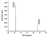
- FIG. 5 is a symmetrical X-ray diffraction diagram of a substrate with ⁇ -type gallium oxide nanorods.
- FIG. 1 is a schematic cross-sectional view showing an example of a substrate with ⁇ -type gallium oxide nanorods according to an embodiment of the present invention.
- FIG. 2 is a schematic configuration diagram showing an example of a manufacturing apparatus used for manufacturing a substrate with ⁇ -
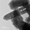
- FIG. 6 is a diagram showing a transmission electron microscope image of ⁇ -type gallium oxide nanorods on a substrate with ⁇ -type gallium oxide nanorods.
- FIG. 7 is a diagram showing a high-magnification transmission electron microscope image of ⁇ -type gallium oxide nanorods on a substrate with ⁇ -type gallium oxide nanorods.
- FIG. 8 shows an atomic force microscope (AFM) image and a reflection high-energy electron diffraction (RHEED) pattern of the surface of a ⁇ -type gallium oxide single crystal substrate with (001) plane orientation treated with oxygen radicals. be.
- AFM atomic force microscope
- RHEED reflection high-energy electron diffraction
- a single crystal substrate means a substrate whose entire substrate is a single crystal.
- oxygen constituent particles are oxygen atoms containing singlet oxygen atoms and triplet oxygen atoms, oxygen molecules, ozone, or particles containing these in an excited state.
- ⁇ indicating a numerical range is used to include the numerical values written before and after it as the lower limit and upper limit.
- a substrate with ⁇ -type gallium oxide nanorods has a substrate having a pair of main surfaces, and a plurality of ⁇ -type gallium oxide nanorods formed on at least one main surface of the substrate, The ⁇ -type gallium oxide nanorods are oriented perpendicularly to the main surface.
- the term " ⁇ -type gallium oxide nanorods vertically aligned" means that the longitudinal direction of the ⁇ -type gallium oxide nanorods is substantially perpendicular to a reference plane. Specifically, this means that the angle of the center line of the nanorod measured with a scanning electron microscope (SEM) is within 90 ⁇ 15° with respect to the main surface, and more preferably within 90 ⁇ 10°.
- FIG. 1 is a schematic cross-sectional view showing an example of a substrate 100 with ⁇ -type gallium oxide nanorods according to an embodiment of the present invention.
- the substrate 100 with ⁇ -type gallium oxide nanorods includes a substrate 110 and a plurality of ⁇ -type gallium oxide nanorods 120 formed on the substrate 110.
- ⁇ -type gallium oxide nanorods 120 are formed on the first main surface 110a of the substrate 110.
- the ⁇ -type gallium oxide nanorods 120 are oriented perpendicularly to the main surface 110a.
- the ⁇ -type gallium oxide nanorods 120 may be provided on at least one main surface of the substrate 110, that is, the first main surface 110a, and may be provided on both main surfaces. However, from the viewpoint of epitaxial growth of the ⁇ -type gallium oxide nanorods 120, the ⁇ -type gallium oxide nanorods 120 are preferably provided only on the first main surface 110a.
- the substrate 110 examples include, but are not limited to, a single crystal substrate, a polycrystalline substrate, a resin substrate, a glass substrate, and the like.
- the substrate 110 is preferably a single crystal substrate from the viewpoint of improving the crystallinity of the ⁇ -type gallium oxide nanorods.
- single crystal substrates include ⁇ -type gallium oxide single crystal substrates, silicon single crystal substrates, gallium nitride single crystal substrates, sapphire single crystal substrates, other oxide single crystal substrates, SiC single crystal substrates, etc. From the viewpoint of improving performance, a ⁇ -type gallium oxide single crystal substrate is preferable, and from the viewpoint of productivity, a silicon single crystal substrate, a sapphire single crystal substrate, or another oxide single crystal substrate is preferable.
- the oxide include MgO, MgAl 2 O 4 , SrTiO 3 , and ZrO 2 .
- ⁇ -type gallium oxide nanorods can be grown on a substrate.
- the ⁇ -type gallium oxide single crystal substrate conventionally known ones can be used, but for example, a substrate grown by crystal growth using the Czochralski method or the floating zone (FZ) method and then cut and polished is preferably used.
- the ⁇ -type gallium oxide single crystal substrate is more preferably a (001) plane-oriented substrate. Further, it is more preferable to form the ⁇ -type gallium oxide nanorods on the (001) plane-oriented main surface as the first main surface.
- resin substrates examples include polyethylene, polypropylene, polyvinyl chloride, polyvinylidene chloride, polystyrene, polyvinyl acetate, polytetrafluoroethylene, ABS (acrylonitrile butadiene styrene) resin, AS (acrylonitrile styrene) resin, and acrylic resin (polymethacrylate).
- thermoplastic resins such as methyl acid, etc.
- thermosetting resins such as phenol resins, epoxy resins, melamine resins, urea resins, unsaturated polyester resins, alkyd resins, polyurethanes, thermosetting polyimides, and silicone rubbers.
- the ⁇ -type gallium oxide nanorods 120 are nanorods formed, for example, by crystal growth, preferably epitaxial growth, of ⁇ -type gallium oxide on a substrate.
- the ⁇ -type gallium oxide nanorods 120 may be nanorods formed by epitaxially growing ⁇ -type gallium oxide on another substrate and transferred onto the substrate 110 by a method that will be exemplified later.
- a plurality of ⁇ -type gallium oxide nanorods 120 are formed on the first main surface 110a of the substrate 110, and are oriented perpendicularly to the first main surface 110a.
- the ⁇ -type gallium oxide nanorods may be single crystal or polycrystalline, but from the viewpoint of the yield and characteristics of semiconductor devices, a single crystal or a crystal close to a single crystal is preferable, and is composed of a single crystal. It is more preferable.
- a crystal close to a single crystal means that the entire nanorod consists of a single crystal with the same atomic arrangement.
- the ⁇ -type gallium oxide nanorods are preferably (001)-oriented single crystals. Note that when n-type or p-type ⁇ -type gallium oxide nanorods are formed by mixing a small amount of impurities, the ⁇ -type gallium oxide nanorods may contain these impurities.
- an index of its crystallinity includes the presence or absence of a peak of ⁇ -type gallium oxide attributed to the (001) plane by symmetric X-ray diffraction.
- a peak attributed to the (001) plane be observed by symmetrical X-ray diffraction.
- Examples of the peak of ⁇ -type gallium oxide attributed to the (001) plane include peaks of the (002) plane, (004) plane, and the like. This makes it possible to confirm the presence of a ⁇ -type gallium oxide nanorod single crystal in the ⁇ -type gallium oxide nanorods.
- symmetrical X-ray diffraction measurement for example, CuK ⁇ rays are used as a radiation source, the X-rays are irradiated onto the surface of the substrate at a Bragg diffraction angle ⁇ , and the diffracted X-rays are detected at a detector at ⁇ -2 ⁇ . Do it by rotating.
- a diffraction peak is obtained at .28°. Therefore, if a diffraction peak is obtained at the above-mentioned Bragg diffraction angle, it can be attributed to the peak of the (001) plane of ⁇ -type gallium oxide.
- the full width at half maximum (FWHM, Full Width Half Maximum) of the peak attributed to the (001) plane is 15 arcsec or more and 50 arcsec or less.
- the crystallinity of the ⁇ -type gallium oxide single crystal can be quantitatively evaluated based on the half-width of such a peak.
- the lower limit of the half-value width is not particularly limited, but, for example, the half-value width is preferably 15 arcsec or more, and more preferably 20 arcsec or more. Such half width can be measured by X-ray diffraction rocking curve measurement.
- substantially no dislocations exist in the ⁇ -type gallium oxide nanorods.
- the substantial absence of dislocations in the ⁇ -type gallium oxide nanorods can be confirmed by observing the ⁇ -type gallium oxide nanorods using a transmission electron microscope. Specifically, if 10 or more nanorods are observed using a transmission electron microscope and no dislocations are observed, it can be determined that there are substantially no dislocations in the ⁇ -type gallium oxide nanorods.
- the height of the ⁇ -type gallium oxide nanorods is preferably 0.5 ⁇ m or more and 50 ⁇ m or less.
- the height of the ⁇ -type gallium oxide nanorod is preferably 0.5 ⁇ m or more, more preferably 0.8 ⁇ m or more, and even more preferably 1 ⁇ m or more, since it is suitable for flowing a sample solution in biological device applications.
- the upper limit of the height of the ⁇ -type gallium oxide nanorods is not particularly limited, but from the viewpoint of productivity and ease of controlling the quality of the ⁇ -type gallium oxide nanorods, the height is preferably 50 ⁇ m or less.
- the height of the ⁇ -type gallium oxide nanorods may be, for example, 0.8 ⁇ m or more and 30 ⁇ m or less, or 1 ⁇ m or more and 20 ⁇ m or less.
- the height of the ⁇ -type gallium oxide nanorods can be determined, for example, by observing a cross section of the substrate with the ⁇ -type gallium oxide nanorods using a scanning electron microscope and measuring the length from the main surface of the substrate to the top of the nanorods. Note that it is preferable that the heights of 10 or more nanorods are measured and the average value thereof is within the above range.
- the thickness of the ⁇ -type gallium oxide nanorods is preferably 10 nm to 200 nm. From the viewpoint of strength, the thickness of the ⁇ -type gallium oxide nanorod is preferably 10 nm or more, more preferably 20 nm or more, even more preferably 30 nm or more, and even more preferably 40 nm or more. On the other hand, from the viewpoint of increasing the density, the thickness of the ⁇ -type gallium oxide nanorods is preferably 200 nm or less, more preferably 150 nm or less, even more preferably 120 nm or less, and even more preferably 100 nm or less.
- the thickness of the ⁇ -type gallium oxide nanorods can be determined, for example, by observing the ⁇ -type gallium oxide nanorods using a transmission electron microscope and measuring the diameter of the ⁇ -type gallium oxide nanorods. Note that it is preferable that the diameters of 10 or more nanorods are measured and the average value is within the above range.
- the density of ⁇ -type gallium oxide nanorods formed per 1 ⁇ m 2 of the main surface of the substrate is preferably 20 to 10,000 nanorods/ ⁇ m 2 .
- the density is preferably 20 lines/ ⁇ m 2 or more, more preferably 50 lines/ ⁇ m 2 or more, even more preferably 80 lines/ ⁇ m 2 or more, and more preferably 100 lines/ ⁇ m 2 or more from the viewpoint of biological device performance and light receiving/emitting device performance. More preferred.
- the density is preferably 10000 lines/ ⁇ m 2 or less, more preferably 1000 lines/ ⁇ m 2 or less, even more preferably 800 lines/ ⁇ m 2 or less, and more preferably 500 lines/ ⁇ m 2 or less from the viewpoint of the difficulty of device production. More preferred.
- the height of the ⁇ -type gallium oxide nanorods can be determined, for example, by observing the surface of the substrate with ⁇ -type gallium oxide nanorods using a scanning electron microscope and measuring the number of nanorods per unit area.
- ⁇ -type gallium oxide nanorods can be formed on a substrate without using a buffer layer. Therefore, a buffer layer may or may not be provided between the ⁇ -type gallium oxide nanorods and the substrate.
- the buffer layer is a layer inserted mainly for the purpose of alleviating lattice mismatch, and is a layer having a thickness of 20 nm or more, for example.
- a nucleation layer may be provided between the ⁇ -type gallium oxide nanorods and the substrate.
- the nucleation layer is a layer inserted for the purpose of promoting crystallization of ⁇ -type gallium oxide, and its thickness is, for example, less than 20 nm, preferably less than 10 nm, and more preferably less than 5 nm.
- the nucleation layer may be a continuous layer or a discontinuous layer. Examples of the nucleation layer include a layer containing an element different from that of the substrate, or a surface-modified layer formed by modifying the surface of the substrate.
- the above-mentioned buffer layer may be, for example, a single crystal film of the material with a predetermined thickness, a layer formed by gradually changing the composition of a mixed crystal of the material and a different material, or a superlattice structure of the material and a different material.
- the nucleation layer refers to a thin film or layer having a lattice constant different from that of the adsorption layer or the material in question.
- the surface modified layer is a layer obtained by modifying the surface of a substrate such as a single crystal substrate, and makes it easier for the nanorods to grow by matching the polarity with the nanorods.
- the presence of a nucleation layer can be determined from the difference in atomic arrangement observed by cross-sectional TEM (transmission electron microscope) observation.
- the substrate with ⁇ -type gallium oxide nanorods according to the embodiment of the present invention has the ⁇ -type gallium oxide nanorods oriented perpendicularly to at least one main surface of the substrate, so that the analyte solution can easily flow in the biological device. It has advantages such as easy formation of a pn junction structure in a light emitting device, and is highly applicable industrially, which is preferable.
- Such a substrate with ⁇ -type gallium oxide nanorods can be suitably used in various applications such as biosensors, biodevices such as biomolecule extraction devices, microchannel devices, ultraviolet light emitting/receiving elements, and radiation detectors.
- the present invention relates to a biomolecule extraction device having a substrate with ⁇ -type gallium oxide nanorods according to an embodiment of the present invention. That is, the biomolecule extraction device according to the embodiment of the present invention has the above-mentioned substrate with ⁇ -type gallium oxide nanorods, includes a microchannel formed on the substrate, and the ⁇ -type gallium oxide nanorods have the above-described ⁇ -type gallium oxide nanorods. It is formed within the microchannel.
- a biomolecule extraction device is a device that can extract biomolecules from a sample by flowing the sample through its microchannel.
- the biomolecules contained in the sample are adsorbed by the ⁇ -type gallium oxide nanorods formed within the microchannel, and the solution other than the adsorbed biomolecules passes through the microchannel. This separates biomolecules from the sample.
- a part of the microchannel or the nanorods may be charged depending on the type of biomolecule to be extracted. Examples of the charging method include applying an electric field to the microchannel, and forming a coating layer on the surface of the ⁇ -type gallium oxide nanorod.
- the microchannel formed on the substrate is not particularly limited as long as it functions as a channel for flowing a sample, but it may be a channel-shaped recess formed on at least one main surface of the substrate, for example. good.
- the depth and width of the microchannel are not particularly limited and can be adjusted depending on the target biomolecule; however, if the spatial volume of the microchannel is made too small, pressure loss tends to increase.
- the depth and width may each be 1 ⁇ m or more.
- a mechanism for introducing or collecting a sample may be provided at an end thereof, as a sample inputting part or a sample collecting part.
- the biomolecule extraction device is similar to the substrate with ⁇ -type gallium oxide nanorods according to the embodiment of the present invention, except that it includes ⁇ -type gallium oxide nanorods in the microchannel formed on the substrate.
- the method for forming ⁇ -type gallium oxide nanorods in a microchannel is not particularly limited. For example, by forming ⁇ -type gallium oxide nanorods on a substrate on which a microchannel has been formed in advance, ⁇ -type gallium oxide nanorods can be formed in a microchannel. Gallium oxide nanorods may also be formed. Further, the substrate with ⁇ -type gallium oxide nanorods on which ⁇ -type gallium oxide nanorods are formed may be processed so that the ⁇ -type gallium oxide nanorods are provided in the microchannel.
- a convex portion on the main surface of the substrate serving as a template. That is, a mold is formed by forming ⁇ -type gallium oxide nanorods on the convex portion, and a material of another substrate is applied and hardened on the main surface of the mold that includes the ⁇ -type gallium oxide nanorods (provided with the convex portion). It is preferable to form another substrate by a method such as.
- the substrate with ⁇ -type gallium oxide nanorods obtained by this method in which the ⁇ -type gallium oxide nanorods are transferred to another substrate, recesses corresponding to the protrusions of the mold are formed on the other substrate, and these are formed as microchannels. Become. Furthermore, since the ⁇ -type gallium oxide nanorods are transferred into the recesses, a biomolecule extraction device including the ⁇ -type gallium oxide nanorods in the microchannel can be obtained. According to this method, the ⁇ -type gallium oxide nanorods to be transferred are embedded in the recesses, and even if the sample inflow speed is increased, the nanowires are difficult to separate from the microchannel, which is preferable. Note that when the ⁇ -type gallium oxide nanorods are transferred by this method, the ⁇ -type gallium oxide nanorods may be grown again after the transfer.
- the above-mentioned resin substrate is suitably used as another substrate.
- a resin for the resin substrate that is light-transmissive and has no affinity with biomolecules.
- the material include cycloolefin polymer (COP), polydimethylsiloxane (PDMS), polymethyl methacrylate (PMMA), polycarbonate (PC), plastics such as hard polyethylene, and silicone.
- Samples used in biomolecule extraction devices include, for example, liquids containing biomolecules as described below, and specifically, culture fluids, body fluids such as serum and urine, and suspensions containing cells, viruses, bacteria, etc. Examples include liquids and the like.
- biomolecules that can be extracted by the biomolecule extraction device include exosomes containing microRNA, and nucleic acids contained in cells, viruses, bacteria, and the like.
- cells include those having a cell membrane structure, such as Staphylococcus, Bacillus subtilis, E. coli, Salmonella, Pseudomonas aeruginosa, Vibrio cholerae, Shigella, Bacillus anthrax, Mycobacterium tuberculosis, Clostridium botulinum, Clostridium tetani, Streptococcus, etc.
- bacteria granulocytes, lymphocytes, reticulocytes, red blood cells, white blood cells, blood cells such as platelets, and the like.
- viruses examples include norovirus, rotavirus, influenza virus, adenovirus, coronavirus, measles virus, rubella virus, hepatitis virus, herpes virus, and HIV.
- examples of the fungus include mushrooms, molds, and yeast, and specific examples include Trichophyton, Candida, Aspergillus, and Yeast.
- mitochondria and extracellular vesicles can also be cited as biomolecules.
- a method for manufacturing a substrate with ⁇ -type gallium oxide nanorods includes, for example, the following steps 1 to 4.
- Step 1 Step of installing a substrate inside the reaction chamber.
- Step 2 A step of turning a mixed gas containing oxygen and ozone into plasma, dissociating the ozone into oxygen constituent particles, and supplying the resulting particles to the reaction chamber under reduced pressure.
- Step 3 Along with Step 2, a step of supplying gallium element to the reaction chamber.
- Step 4 A step of epitaxially growing ⁇ -type gallium oxide nanorods on the substrate.
- the manufacturing apparatus 1000 includes a reaction chamber 1100, a substrate placement section 1200, a gallium element supply device 1300, an oxygen element supply device 1400, and a heating device 1220.
- the reaction chamber 1100 is a place where ⁇ -type gallium oxide nanorods are epitaxially grown on the substrate 110.
- the inside of the reaction chamber 1100 is equipped with a substrate placement section 1200 and a susceptor 1210, and the substrate 110 is placed in the substrate placement section 1200, and the substrate 110 is supported by the susceptor 1210.
- the substrate placement section 1200 in the reaction chamber 1100 can be heated by a heating device 1220, and the substrate 110 can be set to a desired temperature. It is preferable that the temperature of the substrate placement section 1200 be raised to 0° C. or higher, and preferably to room temperature or higher, using a heating device. Further, the upper limit of the heating temperature is not particularly limited, but it is sufficient if it can be heated to, for example, 700°C.
- a gallium element supply device 1300 supplies gallium element (Ga) to the placed substrate 110 .
- This gallium element supply device 1300 is not particularly limited as long as it can supply gallium element, but for example, a Knudsen cell can be mentioned.
- the gallium element supply device 1300 has a shutter 1310, which allows communication between the gallium element supply device 1300 and the reaction chamber 1100 to be made or shut off.
- the gallium element supply device 1300 may include a heating device and a cooling device.
- oxygen constituent particles are supplied to the arranged substrate 110 by an oxygen element supply device 1400.
- This oxygen element supply device 1400 includes a plasma generation section 1450 and, if necessary, a shutter 1410.
- the shutter 1410 allows the oxygen element supply device 1400 and the reaction chamber 1100 to communicate with each other or disconnects them from each other.
- the oxygen element supply device 1400 may include a heating device and a cooling device.
- the oxygen constituent particles supplied to the substrate 110 by the oxygen element supply device 1400 are obtained by converting a mixed gas containing oxygen and ozone into plasma by the plasma generation unit 1450, and dissociating ozone.
- oxygen gas is supplied from the oxygen gas supply unit 1500 toward the oxygen element supply device 1400.
- Oxygen gas passes through an oxygen gas supply pipe 1810 and flows into the ozonizer 1700 while its flow rate is adjusted by a mass flow controller 1820.
- a portion of the oxygen gas that has flowed into the ozonizer 1700 is converted into ozone, resulting in a mixed gas containing oxygen and ozone.
- An example of such an ozonizer 1700 is a first plasma generator that turns oxygen gas into plasma.
- the ozonizer 1700 preferably has the ability to increase the concentration of ozone to the total of oxygen and ozone to 10% by volume or more, more preferably 20% by volume or more, and even more preferably 25% by volume or more. .
- the mixed gas containing oxygen and ozone generated by the ozonizer 1700 passes through the ozone/oxygen mixed gas supply pipe 1830 and flows into the oxygen element supply device 1400 while the flow rate is adjusted by the mass flow controller 1840.
- the ozonizer 1700 and the oxygen element supply device 1400 may be directly connected, and in that case, the ozone-oxygen mixed gas supply pipe 1830 and the mass flow controller 1840 are unnecessary.
- an inert gas is supplied to the oxygen element supply device 1400 from an inert gas supply section 1600.
- the inert gas include rare gases such as Ar gas and He gas.
- the supply of the inert gas is optional.
- the inert gas passes through the inert gas supply pipe 1850 from the inert gas supply section 1600 and flows into the oxygen element supply device 1400 while the flow rate is adjusted by the mass flow controller 1860.
- the mixed gas containing oxygen and ozone and the inert gas may flow into the oxygen element supply device 1400 separately, but as shown in FIG. may be supplied to the oxygen element supply device 1400 in a mixed state.
- the mixed gas supply pipe 1870 is a pipe for supplying a mixed gas containing oxygen and ozone and an inert gas for generating plasma to the oxygen element supply device 1400.
- the inert gas supply section 1600, inert gas supply pipe 1850, and mass flow controller 1860 are unnecessary.
- the manufacturing apparatus 1000 may include an impurity element supply unit (not shown) that supplies impurities.
- the impurity element supply section supplies an impurity element to grow n-type gallium oxide or p-type gallium oxide.
- the impurity element supply section may be, for example, a Knudsen cell; in this case, the Knudsen cell is heated to evaporate, for example, Si or Sn in the case of an n-type, and Mg in the case of a p-type, and the evaporated gas is supplied to the reaction chamber 1100. do. As a result, ⁇ -type gallium oxide doped with these impurity elements can be grown.
- Step 1 the substrate 110 is installed inside the reaction chamber 1100. That is, the substrate 110 is placed on the substrate placement section 1200 and supported by the susceptor 1210. Then, the substrate placement section 1200 is heated using the heating device 1220 to heat the substrate 110 to a desired temperature, and the reaction chamber 1100 is depressurized in preparation for the subsequent step 2. Note that the internal pressure of the reaction chamber 1100 and the temperature of the substrate placement part 1200, that is, the temperature of the substrate 110, are preferably set to the internal pressure and temperature described in (Step 4) described later.
- the various substrates mentioned above can be suitably used.
- a nucleation layer may be formed on the surface of the substrate 110, or ⁇ -type gallium oxide nanorods may be directly formed on the surface of the substrate 110. Formation of the nucleation layer facilitates the growth of ⁇ -type gallium oxide nanorods.
- a method of performing oxygen plasma treatment on the surface of the substrate 110 can be used. Oxygen plasma treatment is a surface treatment in which a mixed gas containing oxygen and ozone is turned into plasma, and the ozone is dissociated into oxygen constituent particles.
- a nucleation layer made of a different material may be formed on the surface of the substrate 110. Examples of the different materials in this case include SiO 2 , Si 3 N 4 , Al 2 O 3 , In 2 O 3 , AlN, GaN, and InN.
- Step 2 a mixed gas containing oxygen and ozone is turned into plasma, and the ozone is dissociated into oxygen constituent particles, which are then supplied to the reaction chamber 1100 under reduced pressure. Specifically, as described above, a part of the oxygen gas supplied from the oxygen gas supply section 1500 to the ozonizer 1700 is plasma-treated by the first plasma generated by the ozonizer 1700 and becomes ozone. A mixed gas containing ozone and ozone is obtained. This is supplied to the oxygen element supply device 1400 via the mixed gas supply pipe 1870.
- the ozonizer 1700 adjusts the concentration of ozone to the total of oxygen and ozone to 10% by volume or more, more preferably 20% by volume or more, and still more preferably 25% by volume or more.
- the upper limit of the ozone concentration is not particularly limited, but is usually 50% by volume or less.
- an inert gas such as Ar gas is supplied from the inert gas supply unit 1600 to the oxygen element supply device 1400 via the mixed gas supply pipe 1870.
- the mixed gas containing oxygen and ozone and the inert gas are mixed inside the mixed gas supply pipe 1870 to form a mixed gas containing oxygen, ozone, and the inert gas.
- the mixing ratio of the mixed gas containing oxygen and ozone and the inert gas is 100 parts by volume of the mixed gas containing oxygen and ozone, and the ratio of the inert gas is 350 parts by volume from the viewpoint of plasma ignition. It is preferably at least 400 parts by volume, more preferably at least 400 parts by volume. Further, from the viewpoint of the density of oxygen radicals, the proportion of the inert gas is preferably 1900 parts by volume or less, more preferably 1500 parts by volume or less, even more preferably 1000 parts by volume or less, and even more preferably 460 parts by volume or less. That is, the proportion of the inert gas is preferably 350 parts by volume to 1900 parts by volume, more preferably 400 parts to 1500 parts by volume, even more preferably 400 parts to 1000 parts by volume, even more preferably 400 parts to 460 parts by volume. preferable.
- oxygen radicals with strong oxidizing power containing a large amount of singlet oxygen atoms O( 1 D) are thought to be generated.
- the oxygen radicals include singlet oxygen atoms O( 1 D) and triplet oxygen atoms O( 3 P). Singlet oxygen atoms O( 1 D) transition to triplet oxygen atoms O( 3 P) at a predetermined rate.
- Ozone dissociated into oxygen molecules and oxygen radicals in this manner is referred to as oxygen constituent particles, and is supplied to the reaction chamber 1100 under reduced pressure. Note that this does not preclude that not only the oxygen constituent particles but also a mixed gas containing non-plasmaized oxygen and ozone may be supplied to the reaction chamber 1100 under reduced pressure.
- step 3 gallium element is supplied to the reaction chamber 1100 under reduced pressure. That is, gallium element (Ga) is supplied from the gallium element supply device 1300 to the reaction chamber 1100 under reduced pressure. As a result, the supplied Ga reacts with the oxygen radicals provided in step 2 on the surface of the substrate 110, and ⁇ -type gallium oxide nanorods are generated on the surface of the substrate 110. Specifically, near the surface of the substrate 110, Ga reacts with singlet oxygen atoms O( 1 D) or triplet oxygen atoms O( 3 P) to which singlet oxygen atoms O( 1 D) have transitioned. , ⁇ -type gallium oxide nanorods grow.
- the gas pressure supplied from the oxygen element supply device 1400 containing oxygen constituent particles in step 2 is preferably 1.0 ⁇ 10 ⁇ 5 Pa or higher, and 1.0 ⁇ 10 ⁇ 4 Pa from the viewpoint of supplying sufficient oxygen radicals.
- the pressure is more preferably 1.0 ⁇ 10 ⁇ 3 Pa or more, and even more preferably 1.0 ⁇ 10 ⁇ 3 Pa or more.
- the gas pressure supplied from the oxygen element supply device 1400 containing oxygen constituent particles in step 2 is preferably 1.0 ⁇ 10 ⁇ 1 Pa or less, and 1.0 ⁇ 10 ⁇ 2 More preferably, it is less than Pa.
- the gas pressure supplied from the oxygen element supply device 1400 is preferably 1.0 ⁇ 10 ⁇ 5 Pa to 1.0 ⁇ 10 ⁇ 1 Pa, and preferably 1.0 ⁇ 10 ⁇ 4 Pa to 1.0 ⁇ 10 ⁇ 1 Pa is more preferable, and 1.0 ⁇ 10 ⁇ 3 Pa to 1.0 ⁇ 10 ⁇ 2 Pa is even more preferable.
- the gas pressure supplied from the gallium element supply device 1300 in step 3 is preferably 1.0 ⁇ 10 -8 Pa or more, more preferably 1.0 ⁇ 10 -7 Pa or more, from the viewpoint of supplying sufficient Ga element. More preferably, it is 1.0 ⁇ 10 ⁇ 6 Pa or more.
- the gas pressure supplied from the gallium element supply device 1300 is high and the amount of Ga element supplied is too large, it becomes thermodynamically difficult to grow ⁇ -type gallium oxide. is preferably 1.0 ⁇ 10 ⁇ 2 Pa or less, more preferably 1.0 ⁇ 10 ⁇ 3 Pa or less.
- the gas pressure supplied from the gallium element supply device 1300 is preferably 1.0 ⁇ 10 ⁇ 8 Pa to 1.0 ⁇ 10 ⁇ 2 Pa, and 1.0 ⁇ 10 ⁇ 7 Pa to 1.0 ⁇ 10 ⁇ 3 Pa is more preferable, and 1.0 ⁇ 10 ⁇ 6 Pa to 1.0 ⁇ 10 ⁇ 3 Pa is even more preferable.
- Step 4 is a step in which ⁇ -type gallium oxide is epitaxially grown on the substrate 110 by the steps 2 and 3 described above.
- the internal pressure of the reaction chamber 1100 is preferably 0.005 Pa or more, more preferably 0.01 Pa or more, from the viewpoint of the exhaust capacity of the apparatus. Further, from the viewpoint of the mean free path of oxygen radicals and gallium, the internal pressure is preferably 0.1 Pa or less, more preferably 0.05 Pa or less. That is, the internal pressure of the reaction chamber 1100 is preferably 0.005 Pa to 0.1 Pa, more preferably 0.01 Pa to 0.05 Pa.
- the temperature of the substrate 110 is preferably 200° C. or higher, more preferably 250° C. or higher, and even more preferably 300° C. or higher, from the viewpoint of crystal growth. Further, from the viewpoint of growth rate, the growth temperature is preferably 500°C or lower, more preferably 400°C or lower. That is, the growth temperature is preferably 200°C to 500°C, more preferably 250°C to 400°C, even more preferably 3000°C to 400°C. Note that the growth temperature is defined, for example, as a set temperature in the heating device 1220.
- the plasma output is preferably 300 W or more, more preferably 350 W or more, and even more preferably 400 W or more.
- the plasma output is preferably 800 W or less, more preferably 750 W or less, and even more preferably 700 W or less.
- the mixed gas in step 3 is supplied to the reaction chamber at a flow rate of 0.2 sccm to 1.0 sccm. It is preferable. From the viewpoint of the amount of oxygen radicals required to generate ⁇ -type gallium oxide, the flow rate is preferably 0.2 sccm or more, more preferably 0.4 sccm or more, and even more preferably 0.6 sccm or more.
- the flow rate is preferably 1.0 sccm or less, more preferably 0.95 sccm or less, and even more preferably 0.90 sccm or less.
- both the plasma output and the flow rate of the mixed gas are within the above ranges.
- Methods for making the ⁇ -type gallium oxide nanorods relatively thick include, for example, increasing the gas pressure supplied from the gallium element supply device, decreasing the supply amount of a mixed gas containing oxygen and ozone, etc. can be mentioned.
- methods for increasing the length of the ⁇ -type gallium oxide nanorods include relatively increasing the growth rate of the ⁇ -type gallium oxide nanorods, increasing the time for crystal growth, and the like.
- Methods for relatively increasing the growth rate of ⁇ -type gallium oxide nanorods include, for example, increasing the gas pressure supplied from the gallium element supply device, increasing the supply amount of a mixed gas containing oxygen and ozone, etc. Can be mentioned.
- Methods for relatively increasing the density of ⁇ -type gallium oxide nanorods include, for example, increasing the growth rate of ⁇ -type gallium oxide nanorods, increasing the supply amount of a mixed gas containing oxygen and ozone, and supplying gallium element. Examples include lowering the gas pressure supplied from the device.
- a substrate with ⁇ -type gallium oxide nanorods according to an embodiment of the present invention can be obtained. According to this method, not only can a substrate with ⁇ -type gallium oxide nanorods having the above-mentioned characteristics be obtained, but also the growth rate in the epitaxial growth of ⁇ -type gallium oxide is fast and a low growth temperature can be used, resulting in excellent productivity.
- ⁇ -type gallium oxide nanorods can be attached to the substrate without requiring a buffer layer. be made to grow upwards.
- a substrate with ⁇ -type gallium oxide nanorods including ⁇ -type gallium oxide nanorods with excellent crystallinity can be obtained.
- a substrate with ⁇ -type gallium oxide nanorods having excellent crystallinity is highly applicable industrially and is preferred.
- ⁇ -type gallium oxide nanorods according to an embodiment of the present invention can be obtained by using a substrate with ⁇ -type gallium oxide nanorods obtained by the above method as a template, and transferring ⁇ -type gallium oxide nanorods included in the template to another substrate. It may also be manufactured by As a method for transferring the ⁇ -type gallium oxide nanorods to another substrate, for example, another substrate is formed by applying and curing the material of another substrate on the surface of the template having the ⁇ -type gallium oxide nanorods. There is a method of transferring the ⁇ -type gallium oxide nanorods onto another substrate by then peeling off the substrate provided in the template.
- the ⁇ -type gallium oxide nanorods may be grown again on another substrate.
- the above-mentioned resin substrate is preferably used, for example.
- the ⁇ -type gallium oxide nanorods included in the template are oriented perpendicularly to the main surface of the substrate, so that they can be oriented perpendicularly to the main surface of another substrate. ⁇ -type gallium oxide nanorods can be obtained.
- ⁇ -type gallium oxide nanorods were epitaxially grown on a ⁇ -type gallium oxide single crystal substrate according to the following procedure to obtain a substrate with ⁇ -type gallium oxide nanorods.
- a ⁇ -type gallium oxide single crystal substrate whose bulk was oriented in the (001) plane was washed with an organic solvent, then washed with an acid, and dried. Thereafter, a ⁇ -type gallium oxide single crystal substrate was placed on the substrate placement section 1200 so that the (001) plane was the surface, and supported by a susceptor 1210. Thereafter, oxygen plasma treatment was performed for 15 minutes under the following conditions.
- Plasma output 600W
- Gas used Ar and mixed gas (O 2 + O 3 )
- Ar flow rate 3.2 sccm
- O2 + O3 flow rate 0.8sccm
- Reaction chamber pressure 6.0 ⁇ 10 ⁇ 5 Torr (8.0 ⁇ 10 ⁇ 3 Pa)
- Substrate temperature set temperature of heating device: 300°C
- the substrate temperature (set temperature of the heating device) was subsequently set to 300° C., and the gas pressure supplied from the gallium element supply device 1300 was set to 8.5 ⁇ 10 ⁇ 7 Torr (1.1 ⁇ 10 ⁇ 4 Pa).
- gallium oxide was epitaxially grown for 60 minutes to obtain a substrate with ⁇ -type gallium oxide nanorods. Note that the pressure inside the reaction chamber during growth was 6.0 ⁇ 10 ⁇ 5 Torr (8.0 ⁇ 10 ⁇ 3 Pa).
- FIG. 3 is a scanning electron micrograph showing the surface of the obtained substrate with ⁇ -type gallium oxide nanorods.
- FIG. 3(a) is a scanning electron micrograph at a magnification of 20,000 times
- FIG. 3(b) is a scanning electron micrograph at a magnification of 50,000 times.
- FIG. 4 is a scanning electron micrograph showing a cross section of the obtained substrate with ⁇ -type gallium oxide nanorods, and the photographing magnification is 20,000 times.
- FIGS. 3 and 4 it was confirmed that the growth on the ⁇ -type gallium oxide single crystal substrate ( ⁇ -type gallium oxide nanorods) had a very beautiful nanorod shape.
- the ⁇ -type gallium oxide nanorods were oriented perpendicularly to the main surface of the ⁇ -type gallium oxide single crystal substrate on which the ⁇ -type gallium oxide nanorods were formed.
- the height of the ⁇ -type gallium oxide nanorods was 1.6 ⁇ m.
- the thickness of the ⁇ -type gallium oxide nanorods was 90 nm.
- the density of ⁇ -type gallium oxide nanorods was about 40/ ⁇ m 2 per 1 ⁇ m 2 of the main surface of the ⁇ -type gallium oxide single crystal substrate.
- the growth rate of the ⁇ -type gallium oxide nanorods was 26.7 nm/min (1.6 ⁇ m/hour).
- ⁇ -type gallium oxide nanorods could be formed at a very fast growth rate on the (001) plane of the ⁇ -type gallium oxide single crystal substrate. Furthermore, the formed ⁇ -type gallium oxide nanorods are columnar, substantially perpendicular to the main surface, and have a relatively uniform diameter, which is very good. Furthermore, the growth temperature is extremely low at 300°C. Conventionally, it has been possible to form ⁇ -type gallium oxide nanorods in a beautiful shape that are oriented perpendicular to the plane formed on the substrate.
- ⁇ -type gallium oxide nanorods composed of Furthermore, it can be said that there is no example in which ⁇ -type gallium oxide nanorods composed of single crystals could be formed at a relatively high growth rate and at a relatively low temperature as in this example.
- a plurality of ⁇ -type gallium oxide nanorods are provided on at least one main surface of a substrate, and the ⁇ -type gallium oxide nanorods are oriented perpendicularly to the main surface. This is the first time that a printed circuit board has been provided, and the effects of the present invention are obvious.
- FIG. 5 is a symmetrical X-ray diffraction diagram of the obtained substrate with ⁇ -type gallium oxide nanorods. The horizontal axis in FIG. 5 is 2 ⁇ - ⁇ , and the vertical axis is intensity.
- FIG. 6 is a diagram showing a transmission electron microscope image of ⁇ -type gallium oxide nanorods on a substrate with ⁇ -type gallium oxide nanorods, and the observation magnification is 250,000 times.
- FIG. 7 is a diagram showing a high-magnification transmission electron microscope image of ⁇ -type gallium oxide nanorods on a substrate with ⁇ -type gallium oxide nanorods, and the observation magnification is 600,000 times.
- FIGS. 7(a) and 7(b) are diagrams showing the arrangement of the atomic planes of ⁇ -type gallium oxide nanorods at different observation positions, respectively.
- FIG. 8 shows an atomic force microscope (AFM) image and a reflection high-speed electron diffraction (RHEED) pattern of the surface of a ⁇ -type gallium oxide single crystal substrate with (001) plane orientation treated with oxygen radicals. It is a diagram.
- FIG. 8(a) is a diagram showing an atomic force microscope (AFM) image
- FIG. 8(b) is a diagram showing a reflection high-speed electron diffraction (RHEED) pattern. From FIG. 8, it was confirmed that the surface condition of the ⁇ -type gallium oxide single crystal substrate before growing ⁇ -type gallium oxide was good due to the surface treatment with oxygen radicals.
- the ⁇ -type gallium oxide single-crystal nanorods grown on the (001)-oriented ⁇ -type gallium oxide single-crystal substrate by the above method were (001)-oriented single crystals. According to the present invention, it is possible to produce ⁇ -type gallium oxide single crystal nanorods that are nearly perfect crystals with almost no dislocations, and therefore have high industrial applicability.
- a substrate having a pair of main surfaces, and a plurality of ⁇ -type gallium oxide nanorods formed on at least one main surface of the substrate, A substrate with ⁇ -type gallium oxide nanorods, wherein the ⁇ -type gallium oxide nanorods are oriented perpendicularly to the main surface.
- 3. The substrate with ⁇ -type gallium oxide nanorods according to 1 or 2 above, wherein the substrate is a single crystal substrate. 4. 4.
- 9. The substrate with ⁇ -type gallium oxide nanorods according to any one of 1 to 8 above, wherein the ⁇ -type gallium oxide nanorods have a thickness of 10 nm to 200 nm. 10.
- a method for manufacturing a substrate with ⁇ -type gallium oxide nanorods the method comprising epitaxially growing a plurality of ⁇ -type gallium oxide nanorods on the substrate. 13. 13. The method for manufacturing a substrate with ⁇ -type gallium oxide nanorods as described in 12 above, wherein the plasma generation is performed at a plasma output of 300W to 800W. 14. 14.
- Substrate 110 with ⁇ -type gallium oxide nanorods Substrate 110a First main surface 120 ⁇ -type gallium oxide nanorods 1000 Manufacturing device 1100 Reaction chamber 1200 Substrate placement section 1210 Susceptor 1220 Heating device 1300 Gallium element supply device 1310, 1410 Shutter 1400 Oxygen element supply device 1450 Plasma generation section 1500 Oxygen gas supply section 1600 Inert gas supply section 1700 Ozonizer 1810 Oxygen gas supply pipe 1820, 1840, 1860 Mass flow controller 1830 Ozone oxygen mixed gas supply pipe 1850 Inert gas supply pipe 1870 Mixed gas supply pipe
Landscapes
- Chemical & Material Sciences (AREA)
- Engineering & Computer Science (AREA)
- Health & Medical Sciences (AREA)
- Organic Chemistry (AREA)
- Life Sciences & Earth Sciences (AREA)
- Metallurgy (AREA)
- Materials Engineering (AREA)
- Bioinformatics & Cheminformatics (AREA)
- Biotechnology (AREA)
- Immunology (AREA)
- Biomedical Technology (AREA)
- Crystallography & Structural Chemistry (AREA)
- Wood Science & Technology (AREA)
- Hematology (AREA)
- General Health & Medical Sciences (AREA)
- General Physics & Mathematics (AREA)
- Biochemistry (AREA)
- Chemical Kinetics & Catalysis (AREA)
- Zoology (AREA)
- Mechanical Engineering (AREA)
- Physics & Mathematics (AREA)
- Inorganic Chemistry (AREA)
- Urology & Nephrology (AREA)
- Microbiology (AREA)
- Medicinal Chemistry (AREA)
- Molecular Biology (AREA)
- Cell Biology (AREA)
- Pathology (AREA)
- General Chemical & Material Sciences (AREA)
- Food Science & Technology (AREA)
- Sustainable Development (AREA)
- Analytical Chemistry (AREA)
- Genetics & Genomics (AREA)
- General Engineering & Computer Science (AREA)
- Condensed Matter Physics & Semiconductors (AREA)
- Manufacturing & Machinery (AREA)
- Computer Hardware Design (AREA)
- Microelectronics & Electronic Packaging (AREA)
- Power Engineering (AREA)
- Crystals, And After-Treatments Of Crystals (AREA)
Abstract
La présente invention concerne un substrat avec des nano-tiges d'oxyde de gallium de type β qui comprend : un substrat ayant une paire de surfaces principales ; et une pluralité de nano-tiges d'oxyde de gallium de type β qui sont formées sur le substrat. Les nanotiges d'oxyde de gallium de type β sont disposées en réseau de manière à être perpendiculaires à au moins l'une des surfaces principales du substrat.
Applications Claiming Priority (4)
| Application Number | Priority Date | Filing Date | Title |
|---|---|---|---|
| JP2022050538 | 2022-03-25 | ||
| JP2022-050538 | 2022-03-25 | ||
| JP2022-119938 | 2022-07-27 | ||
| JP2022119938 | 2022-07-27 |
Publications (1)
| Publication Number | Publication Date |
|---|---|
| WO2023182313A1 true WO2023182313A1 (fr) | 2023-09-28 |
Family
ID=88101091
Family Applications (1)
| Application Number | Title | Priority Date | Filing Date |
|---|---|---|---|
| PCT/JP2023/011021 WO2023182313A1 (fr) | 2022-03-25 | 2023-03-20 | SUBSTRAT AVEC NANO-TIGES D'OXYDE DE GALLIUM DE TYPE β, PROCÉDÉ DE FABRICATION DUDIT SUBSTRAT ET DISPOSITIF D'EXTRACTION DE BIOMOLÉCULES |
Country Status (1)
| Country | Link |
|---|---|
| WO (1) | WO2023182313A1 (fr) |
Citations (6)
| Publication number | Priority date | Publication date | Assignee | Title |
|---|---|---|---|---|
| JP2005239524A (ja) * | 2004-02-27 | 2005-09-08 | Japan Science & Technology Agency | β−Ga2O3ナノロッドとその製造方法 |
| JP2016051796A (ja) * | 2014-08-29 | 2016-04-11 | 株式会社タムラ製作所 | 半導体素子及びその製造方法 |
| JP2016064961A (ja) * | 2014-09-25 | 2016-04-28 | 株式会社Flosfia | 結晶性積層構造体の製造方法および半導体装置 |
| JP2019067915A (ja) * | 2017-09-29 | 2019-04-25 | 株式会社タムラ製作所 | 電界効果トランジスタ |
| WO2020071175A1 (fr) * | 2018-10-04 | 2020-04-09 | 株式会社Adeka | Matière première servant à la formation de film mince destinée à être utilisée dans un procédé de dépôt de couche atomique, matière première servant à la formation de film mince, procédé de production de film mince, et composé |
| WO2021131331A1 (fr) * | 2019-12-23 | 2021-07-01 | 国立研究開発法人物質・材料研究機構 | Puce d'inspection biomoléculaire pour détection de fluorescence |
-
2023
- 2023-03-20 WO PCT/JP2023/011021 patent/WO2023182313A1/fr unknown
Patent Citations (6)
| Publication number | Priority date | Publication date | Assignee | Title |
|---|---|---|---|---|
| JP2005239524A (ja) * | 2004-02-27 | 2005-09-08 | Japan Science & Technology Agency | β−Ga2O3ナノロッドとその製造方法 |
| JP2016051796A (ja) * | 2014-08-29 | 2016-04-11 | 株式会社タムラ製作所 | 半導体素子及びその製造方法 |
| JP2016064961A (ja) * | 2014-09-25 | 2016-04-28 | 株式会社Flosfia | 結晶性積層構造体の製造方法および半導体装置 |
| JP2019067915A (ja) * | 2017-09-29 | 2019-04-25 | 株式会社タムラ製作所 | 電界効果トランジスタ |
| WO2020071175A1 (fr) * | 2018-10-04 | 2020-04-09 | 株式会社Adeka | Matière première servant à la formation de film mince destinée à être utilisée dans un procédé de dépôt de couche atomique, matière première servant à la formation de film mince, procédé de production de film mince, et composé |
| WO2021131331A1 (fr) * | 2019-12-23 | 2021-07-01 | 国立研究開発法人物質・材料研究機構 | Puce d'inspection biomoléculaire pour détection de fluorescence |
Similar Documents
| Publication | Publication Date | Title |
|---|---|---|
| Kong et al. | Growth rate, surface morphology, and defect microstructures of β–SiC films chemically vapor deposited on 6H–SiC substrates | |
| Chichibu et al. | Helicon-wave-excited-plasma sputtering epitaxy of ZnO on sapphire (0001) substrates | |
| Chen et al. | ZnO thin films synthesized by chemical vapor deposition | |
| JP2008303119A (ja) | 高機能性Ga2O3単結晶膜及びその製造方法 | |
| CN101941681A (zh) | 制备带隙单调连续变化的硫硒化镉纳米材料的方法及装置 | |
| Osipov et al. | Structural and optical properties of high quality ZnO thin film on Si with SiC buffer layer | |
| Zhang et al. | Routes to grow well‐aligned arrays of ZnSe nanowires and nanorods | |
| Liu et al. | Crystallography and cathodoluminescence of pyramid-like GaN nanorods epitaxially grown on a sapphire substrate | |
| WO2023182313A1 (fr) | SUBSTRAT AVEC NANO-TIGES D'OXYDE DE GALLIUM DE TYPE β, PROCÉDÉ DE FABRICATION DUDIT SUBSTRAT ET DISPOSITIF D'EXTRACTION DE BIOMOLÉCULES | |
| Zeghouane et al. | Formation of voids in selective area growth of InN nanorods in SiNx on GaN templates | |
| Xia et al. | Growth rate control and phase diagram of wafer-scale Ga2O3 films by MOCVD | |
| Xue et al. | Fabrication of GaN nanowires by ammoniating Ga2O3/Al2O3 thin films deposited on Si (111) with radio frequency magnetron sputtering | |
| WO2023182312A1 (fr) | SUBSTRAT AVEC FILM D'OXYDE DE β-GALLIUM ET SON PROCÉDÉ DE PRODUCTION | |
| El‐Shaer et al. | CBE growth of high‐quality ZnO epitaxial layers | |
| Hu et al. | Synthesis and Photoluminscence Properties of Morphology-and Microstructure-Controlled S-Doped ZnO Nanostructures | |
| Nishitani-Gamo et al. | Interfacial structures of oriented diamond on Si (100) characterized by confocal Raman spectroscopy | |
| CN114108087B (zh) | 一种正交相五氧化二钽单晶薄膜的制备方法 | |
| CN113308741B (zh) | 一种氮化镓单晶材料、其制备方法及应用 | |
| CN105019028B (zh) | 一种制备特定形貌和晶体结构的InAs纳米线的方法 | |
| Kong et al. | Growth and microstructural characterization of catalyst-free ZnO nanostructures grown on sapphire and GaN by thermal evaporation | |
| CN113380603B (zh) | 高硼组分二维iii族多元氮化物混合晶体及其制备方法 | |
| Liu et al. | Homoepitaxial growth of high-quality GaN nanoarrays for enhanced UV luminescence | |
| Jiang et al. | Epitaxy of diamond on Si (100) and surface-roughening-induced crystal misorientation | |
| Bakin | SiC Homoepitaxy and Heteroepitaxy | |
| Chubenko et al. | Seed layer assisted hydrothermal deposition of low-resistivity ZnO thin films |
Legal Events
| Date | Code | Title | Description |
|---|---|---|---|
| 121 | Ep: the epo has been informed by wipo that ep was designated in this application |
Ref document number: 23774908 Country of ref document: EP Kind code of ref document: A1 |