WO2023182313A1 - SUBSTRATE WITH β-TYPE GALLIUM OXIDE NANO-RODS, MANUFACTURING METHOD SAID SUBSTRATE, AND BIOMOLECULE EXTRACTION DEVICE - Google Patents
SUBSTRATE WITH β-TYPE GALLIUM OXIDE NANO-RODS, MANUFACTURING METHOD SAID SUBSTRATE, AND BIOMOLECULE EXTRACTION DEVICE Download PDFInfo
- Publication number
- WO2023182313A1 WO2023182313A1 PCT/JP2023/011021 JP2023011021W WO2023182313A1 WO 2023182313 A1 WO2023182313 A1 WO 2023182313A1 JP 2023011021 W JP2023011021 W JP 2023011021W WO 2023182313 A1 WO2023182313 A1 WO 2023182313A1
- Authority
- WO
- WIPO (PCT)
- Prior art keywords
- gallium oxide
- substrate
- type gallium
- oxide nanorods
- nanorods
- Prior art date
Links
- AJNVQOSZGJRYEI-UHFFFAOYSA-N digallium;oxygen(2-) Chemical compound [O-2].[O-2].[O-2].[Ga+3].[Ga+3] AJNVQOSZGJRYEI-UHFFFAOYSA-N 0.000 title claims abstract description 332
- 229910001195 gallium oxide Inorganic materials 0.000 title claims abstract description 331
- 239000002073 nanorod Substances 0.000 title claims abstract description 295
- 239000000758 substrate Substances 0.000 title claims abstract description 285
- 238000004519 manufacturing process Methods 0.000 title claims description 46
- 238000000605 extraction Methods 0.000 title claims description 17
- 239000001301 oxygen Substances 0.000 claims description 88
- 229910052760 oxygen Inorganic materials 0.000 claims description 88
- QVGXLLKOCUKJST-UHFFFAOYSA-N atomic oxygen Chemical compound [O] QVGXLLKOCUKJST-UHFFFAOYSA-N 0.000 claims description 73
- 239000013078 crystal Substances 0.000 claims description 73
- 239000007789 gas Substances 0.000 claims description 58
- 238000000034 method Methods 0.000 claims description 51
- CBENFWSGALASAD-UHFFFAOYSA-N Ozone Chemical compound [O-][O+]=O CBENFWSGALASAD-UHFFFAOYSA-N 0.000 claims description 49
- 238000006243 chemical reaction Methods 0.000 claims description 36
- 229910052733 gallium Inorganic materials 0.000 claims description 27
- GYHNNYVSQQEPJS-UHFFFAOYSA-N Gallium Chemical compound [Ga] GYHNNYVSQQEPJS-UHFFFAOYSA-N 0.000 claims description 26
- 239000002245 particle Substances 0.000 claims description 15
- 239000000470 constituent Substances 0.000 claims description 13
- 238000002441 X-ray diffraction Methods 0.000 claims description 12
- 238000009832 plasma treatment Methods 0.000 claims description 7
- 239000000203 mixture Substances 0.000 claims description 4
- 239000010410 layer Substances 0.000 description 30
- 239000011261 inert gas Substances 0.000 description 23
- MYMOFIZGZYHOMD-UHFFFAOYSA-N Dioxygen Chemical compound O=O MYMOFIZGZYHOMD-UHFFFAOYSA-N 0.000 description 20
- 239000000463 material Substances 0.000 description 16
- 238000010586 diagram Methods 0.000 description 12
- 229910001882 dioxygen Inorganic materials 0.000 description 12
- 238000010438 heat treatment Methods 0.000 description 11
- 230000005540 biological transmission Effects 0.000 description 10
- 238000010899 nucleation Methods 0.000 description 10
- 230000006911 nucleation Effects 0.000 description 10
- 239000000523 sample Substances 0.000 description 10
- 229920005989 resin Polymers 0.000 description 9
- 239000011347 resin Substances 0.000 description 9
- -1 and at that time Chemical compound 0.000 description 8
- 210000004027 cell Anatomy 0.000 description 8
- 239000012535 impurity Substances 0.000 description 8
- 125000004430 oxygen atom Chemical group O* 0.000 description 6
- 238000001878 scanning electron micrograph Methods 0.000 description 6
- 239000002070 nanowire Substances 0.000 description 5
- 241000700605 Viruses Species 0.000 description 4
- 238000001000 micrograph Methods 0.000 description 4
- 239000004065 semiconductor Substances 0.000 description 4
- 238000012546 transfer Methods 0.000 description 4
- 241000894006 Bacteria Species 0.000 description 3
- 229910005191 Ga 2 O 3 Inorganic materials 0.000 description 3
- 229910002601 GaN Inorganic materials 0.000 description 3
- 238000000089 atomic force micrograph Methods 0.000 description 3
- 230000015572 biosynthetic process Effects 0.000 description 3
- 239000010408 film Substances 0.000 description 3
- 238000005259 measurement Methods 0.000 description 3
- 230000005855 radiation Effects 0.000 description 3
- 238000002128 reflection high energy electron diffraction Methods 0.000 description 3
- 229910052710 silicon Inorganic materials 0.000 description 3
- 229920000089 Cyclic olefin copolymer Polymers 0.000 description 2
- 239000004698 Polyethylene Substances 0.000 description 2
- 240000004808 Saccharomyces cerevisiae Species 0.000 description 2
- XUIMIQQOPSSXEZ-UHFFFAOYSA-N Silicon Chemical compound [Si] XUIMIQQOPSSXEZ-UHFFFAOYSA-N 0.000 description 2
- 239000002253 acid Substances 0.000 description 2
- XECAHXYUAAWDEL-UHFFFAOYSA-N acrylonitrile butadiene styrene Chemical compound C=CC=C.C=CC#N.C=CC1=CC=CC=C1 XECAHXYUAAWDEL-UHFFFAOYSA-N 0.000 description 2
- 239000004676 acrylonitrile butadiene styrene Substances 0.000 description 2
- 229920000122 acrylonitrile butadiene styrene Polymers 0.000 description 2
- 229920001893 acrylonitrile styrene Polymers 0.000 description 2
- 239000012491 analyte Substances 0.000 description 2
- 230000008901 benefit Effects 0.000 description 2
- 238000001816 cooling Methods 0.000 description 2
- 239000004205 dimethyl polysiloxane Substances 0.000 description 2
- 238000002003 electron diffraction Methods 0.000 description 2
- 238000005516 engineering process Methods 0.000 description 2
- 210000001808 exosome Anatomy 0.000 description 2
- 239000007788 liquid Substances 0.000 description 2
- 238000002156 mixing Methods 0.000 description 2
- 238000012986 modification Methods 0.000 description 2
- 230000004048 modification Effects 0.000 description 2
- 238000001451 molecular beam epitaxy Methods 0.000 description 2
- 229920000435 poly(dimethylsiloxane) Polymers 0.000 description 2
- 229920003229 poly(methyl methacrylate) Polymers 0.000 description 2
- 229920000573 polyethylene Polymers 0.000 description 2
- 239000004926 polymethyl methacrylate Substances 0.000 description 2
- SCUZVMOVTVSBLE-UHFFFAOYSA-N prop-2-enenitrile;styrene Chemical compound C=CC#N.C=CC1=CC=CC=C1 SCUZVMOVTVSBLE-UHFFFAOYSA-N 0.000 description 2
- 229910052594 sapphire Inorganic materials 0.000 description 2
- 239000010980 sapphire Substances 0.000 description 2
- 239000010703 silicon Substances 0.000 description 2
- 238000004381 surface treatment Methods 0.000 description 2
- 229920001187 thermosetting polymer Polymers 0.000 description 2
- 229920000178 Acrylic resin Polymers 0.000 description 1
- 239000004925 Acrylic resin Substances 0.000 description 1
- 235000001674 Agaricus brunnescens Nutrition 0.000 description 1
- 229910018072 Al 2 O 3 Inorganic materials 0.000 description 1
- 241000228212 Aspergillus Species 0.000 description 1
- 241000193738 Bacillus anthracis Species 0.000 description 1
- 244000063299 Bacillus subtilis Species 0.000 description 1
- 235000014469 Bacillus subtilis Nutrition 0.000 description 1
- 241000222120 Candida <Saccharomycetales> Species 0.000 description 1
- 241000193155 Clostridium botulinum Species 0.000 description 1
- 241000193449 Clostridium tetani Species 0.000 description 1
- 241000711573 Coronaviridae Species 0.000 description 1
- 241000588724 Escherichia coli Species 0.000 description 1
- 241000233866 Fungi Species 0.000 description 1
- JMASRVWKEDWRBT-UHFFFAOYSA-N Gallium nitride Chemical compound [Ga]#N JMASRVWKEDWRBT-UHFFFAOYSA-N 0.000 description 1
- 241000712079 Measles morbillivirus Species 0.000 description 1
- 229920000877 Melamine resin Polymers 0.000 description 1
- 229910020068 MgAl Inorganic materials 0.000 description 1
- 108700011259 MicroRNAs Proteins 0.000 description 1
- 241000187479 Mycobacterium tuberculosis Species 0.000 description 1
- 241001263478 Norovirus Species 0.000 description 1
- 239000004642 Polyimide Substances 0.000 description 1
- 239000004743 Polypropylene Substances 0.000 description 1
- 239000004793 Polystyrene Substances 0.000 description 1
- 229920001328 Polyvinylidene chloride Polymers 0.000 description 1
- 241000589517 Pseudomonas aeruginosa Species 0.000 description 1
- 241000702670 Rotavirus Species 0.000 description 1
- 241000710799 Rubella virus Species 0.000 description 1
- 241000607142 Salmonella Species 0.000 description 1
- 241000607768 Shigella Species 0.000 description 1
- 229910004298 SiO 2 Inorganic materials 0.000 description 1
- 241000580858 Simian-Human immunodeficiency virus Species 0.000 description 1
- 229910002367 SrTiO Inorganic materials 0.000 description 1
- 241000191940 Staphylococcus Species 0.000 description 1
- 241000194017 Streptococcus Species 0.000 description 1
- 241000223238 Trichophyton Species 0.000 description 1
- 229920001807 Urea-formaldehyde Polymers 0.000 description 1
- 241000607626 Vibrio cholerae Species 0.000 description 1
- 229920000180 alkyd Polymers 0.000 description 1
- 238000004458 analytical method Methods 0.000 description 1
- 210000000601 blood cell Anatomy 0.000 description 1
- 210000001124 body fluid Anatomy 0.000 description 1
- 239000010839 body fluid Substances 0.000 description 1
- 230000015556 catabolic process Effects 0.000 description 1
- 210000002390 cell membrane structure Anatomy 0.000 description 1
- 239000011247 coating layer Substances 0.000 description 1
- 238000004891 communication Methods 0.000 description 1
- 238000002425 crystallisation Methods 0.000 description 1
- 230000008025 crystallization Effects 0.000 description 1
- 239000012531 culture fluid Substances 0.000 description 1
- 230000003247 decreasing effect Effects 0.000 description 1
- 230000000694 effects Effects 0.000 description 1
- 230000005684 electric field Effects 0.000 description 1
- 239000003822 epoxy resin Substances 0.000 description 1
- 210000003743 erythrocyte Anatomy 0.000 description 1
- 230000005281 excited state Effects 0.000 description 1
- 238000007667 floating Methods 0.000 description 1
- 150000002258 gallium Chemical class 0.000 description 1
- QZQVBEXLDFYHSR-UHFFFAOYSA-N gallium(III) oxide Inorganic materials O=[Ga]O[Ga]=O QZQVBEXLDFYHSR-UHFFFAOYSA-N 0.000 description 1
- 239000011521 glass Substances 0.000 description 1
- 210000003714 granulocyte Anatomy 0.000 description 1
- LNEPOXFFQSENCJ-UHFFFAOYSA-N haloperidol Chemical compound C1CC(O)(C=2C=CC(Cl)=CC=2)CCN1CCCC(=O)C1=CC=C(F)C=C1 LNEPOXFFQSENCJ-UHFFFAOYSA-N 0.000 description 1
- 208000006454 hepatitis Diseases 0.000 description 1
- 231100000283 hepatitis Toxicity 0.000 description 1
- 210000000265 leukocyte Anatomy 0.000 description 1
- 210000004698 lymphocyte Anatomy 0.000 description 1
- 230000007246 mechanism Effects 0.000 description 1
- 125000002496 methyl group Chemical group [H]C([H])([H])* 0.000 description 1
- 239000002679 microRNA Substances 0.000 description 1
- 210000003470 mitochondria Anatomy 0.000 description 1
- 108020004707 nucleic acids Proteins 0.000 description 1
- 150000007523 nucleic acids Chemical class 0.000 description 1
- 102000039446 nucleic acids Human genes 0.000 description 1
- 230000003287 optical effect Effects 0.000 description 1
- 239000003960 organic solvent Substances 0.000 description 1
- 230000003647 oxidation Effects 0.000 description 1
- 238000007254 oxidation reaction Methods 0.000 description 1
- 230000001590 oxidative effect Effects 0.000 description 1
- 150000002926 oxygen Chemical class 0.000 description 1
- 239000005011 phenolic resin Substances 0.000 description 1
- 229920003023 plastic Polymers 0.000 description 1
- 239000004033 plastic Substances 0.000 description 1
- 239000004417 polycarbonate Substances 0.000 description 1
- 229920000515 polycarbonate Polymers 0.000 description 1
- 229920000647 polyepoxide Polymers 0.000 description 1
- 229920001721 polyimide Polymers 0.000 description 1
- 229920000193 polymethacrylate Polymers 0.000 description 1
- 229920001155 polypropylene Polymers 0.000 description 1
- 229920001296 polysiloxane Polymers 0.000 description 1
- 229920002223 polystyrene Polymers 0.000 description 1
- 239000004810 polytetrafluoroethylene Substances 0.000 description 1
- 229920001343 polytetrafluoroethylene Polymers 0.000 description 1
- 229920002635 polyurethane Polymers 0.000 description 1
- 239000004814 polyurethane Substances 0.000 description 1
- 229920002689 polyvinyl acetate Polymers 0.000 description 1
- 239000011118 polyvinyl acetate Substances 0.000 description 1
- 239000004800 polyvinyl chloride Substances 0.000 description 1
- 229920000915 polyvinyl chloride Polymers 0.000 description 1
- 239000005033 polyvinylidene chloride Substances 0.000 description 1
- 238000002360 preparation method Methods 0.000 description 1
- 230000008569 process Effects 0.000 description 1
- 230000001737 promoting effect Effects 0.000 description 1
- 210000001995 reticulocyte Anatomy 0.000 description 1
- 239000012488 sample solution Substances 0.000 description 1
- 210000002966 serum Anatomy 0.000 description 1
- 229920002379 silicone rubber Polymers 0.000 description 1
- 238000001179 sorption measurement Methods 0.000 description 1
- 239000000725 suspension Substances 0.000 description 1
- 229920005992 thermoplastic resin Polymers 0.000 description 1
- 239000010409 thin film Substances 0.000 description 1
- 230000007704 transition Effects 0.000 description 1
- 241000701161 unidentified adenovirus Species 0.000 description 1
- 241001529453 unidentified herpesvirus Species 0.000 description 1
- 241000712461 unidentified influenza virus Species 0.000 description 1
- 229920006337 unsaturated polyester resin Polymers 0.000 description 1
- 210000002700 urine Anatomy 0.000 description 1
- 229940118696 vibrio cholerae Drugs 0.000 description 1
Images


Classifications
-
- C—CHEMISTRY; METALLURGY
- C12—BIOCHEMISTRY; BEER; SPIRITS; WINE; VINEGAR; MICROBIOLOGY; ENZYMOLOGY; MUTATION OR GENETIC ENGINEERING
- C12M—APPARATUS FOR ENZYMOLOGY OR MICROBIOLOGY; APPARATUS FOR CULTURING MICROORGANISMS FOR PRODUCING BIOMASS, FOR GROWING CELLS OR FOR OBTAINING FERMENTATION OR METABOLIC PRODUCTS, i.e. BIOREACTORS OR FERMENTERS
- C12M1/00—Apparatus for enzymology or microbiology
-
- C—CHEMISTRY; METALLURGY
- C23—COATING METALLIC MATERIAL; COATING MATERIAL WITH METALLIC MATERIAL; CHEMICAL SURFACE TREATMENT; DIFFUSION TREATMENT OF METALLIC MATERIAL; COATING BY VACUUM EVAPORATION, BY SPUTTERING, BY ION IMPLANTATION OR BY CHEMICAL VAPOUR DEPOSITION, IN GENERAL; INHIBITING CORROSION OF METALLIC MATERIAL OR INCRUSTATION IN GENERAL
- C23C—COATING METALLIC MATERIAL; COATING MATERIAL WITH METALLIC MATERIAL; SURFACE TREATMENT OF METALLIC MATERIAL BY DIFFUSION INTO THE SURFACE, BY CHEMICAL CONVERSION OR SUBSTITUTION; COATING BY VACUUM EVAPORATION, BY SPUTTERING, BY ION IMPLANTATION OR BY CHEMICAL VAPOUR DEPOSITION, IN GENERAL
- C23C14/00—Coating by vacuum evaporation, by sputtering or by ion implantation of the coating forming material
- C23C14/06—Coating by vacuum evaporation, by sputtering or by ion implantation of the coating forming material characterised by the coating material
- C23C14/08—Oxides
-
- C—CHEMISTRY; METALLURGY
- C23—COATING METALLIC MATERIAL; COATING MATERIAL WITH METALLIC MATERIAL; CHEMICAL SURFACE TREATMENT; DIFFUSION TREATMENT OF METALLIC MATERIAL; COATING BY VACUUM EVAPORATION, BY SPUTTERING, BY ION IMPLANTATION OR BY CHEMICAL VAPOUR DEPOSITION, IN GENERAL; INHIBITING CORROSION OF METALLIC MATERIAL OR INCRUSTATION IN GENERAL
- C23C—COATING METALLIC MATERIAL; COATING MATERIAL WITH METALLIC MATERIAL; SURFACE TREATMENT OF METALLIC MATERIAL BY DIFFUSION INTO THE SURFACE, BY CHEMICAL CONVERSION OR SUBSTITUTION; COATING BY VACUUM EVAPORATION, BY SPUTTERING, BY ION IMPLANTATION OR BY CHEMICAL VAPOUR DEPOSITION, IN GENERAL
- C23C16/00—Chemical coating by decomposition of gaseous compounds, without leaving reaction products of surface material in the coating, i.e. chemical vapour deposition [CVD] processes
- C23C16/22—Chemical coating by decomposition of gaseous compounds, without leaving reaction products of surface material in the coating, i.e. chemical vapour deposition [CVD] processes characterised by the deposition of inorganic material, other than metallic material
- C23C16/30—Deposition of compounds, mixtures or solid solutions, e.g. borides, carbides, nitrides
- C23C16/40—Oxides
-
- C—CHEMISTRY; METALLURGY
- C30—CRYSTAL GROWTH
- C30B—SINGLE-CRYSTAL GROWTH; UNIDIRECTIONAL SOLIDIFICATION OF EUTECTIC MATERIAL OR UNIDIRECTIONAL DEMIXING OF EUTECTOID MATERIAL; REFINING BY ZONE-MELTING OF MATERIAL; PRODUCTION OF A HOMOGENEOUS POLYCRYSTALLINE MATERIAL WITH DEFINED STRUCTURE; SINGLE CRYSTALS OR HOMOGENEOUS POLYCRYSTALLINE MATERIAL WITH DEFINED STRUCTURE; AFTER-TREATMENT OF SINGLE CRYSTALS OR A HOMOGENEOUS POLYCRYSTALLINE MATERIAL WITH DEFINED STRUCTURE; APPARATUS THEREFOR
- C30B23/00—Single-crystal growth by condensing evaporated or sublimed materials
- C30B23/02—Epitaxial-layer growth
-
- C—CHEMISTRY; METALLURGY
- C30—CRYSTAL GROWTH
- C30B—SINGLE-CRYSTAL GROWTH; UNIDIRECTIONAL SOLIDIFICATION OF EUTECTIC MATERIAL OR UNIDIRECTIONAL DEMIXING OF EUTECTOID MATERIAL; REFINING BY ZONE-MELTING OF MATERIAL; PRODUCTION OF A HOMOGENEOUS POLYCRYSTALLINE MATERIAL WITH DEFINED STRUCTURE; SINGLE CRYSTALS OR HOMOGENEOUS POLYCRYSTALLINE MATERIAL WITH DEFINED STRUCTURE; AFTER-TREATMENT OF SINGLE CRYSTALS OR A HOMOGENEOUS POLYCRYSTALLINE MATERIAL WITH DEFINED STRUCTURE; APPARATUS THEREFOR
- C30B29/00—Single crystals or homogeneous polycrystalline material with defined structure characterised by the material or by their shape
- C30B29/10—Inorganic compounds or compositions
- C30B29/16—Oxides
-
- C—CHEMISTRY; METALLURGY
- C30—CRYSTAL GROWTH
- C30B—SINGLE-CRYSTAL GROWTH; UNIDIRECTIONAL SOLIDIFICATION OF EUTECTIC MATERIAL OR UNIDIRECTIONAL DEMIXING OF EUTECTOID MATERIAL; REFINING BY ZONE-MELTING OF MATERIAL; PRODUCTION OF A HOMOGENEOUS POLYCRYSTALLINE MATERIAL WITH DEFINED STRUCTURE; SINGLE CRYSTALS OR HOMOGENEOUS POLYCRYSTALLINE MATERIAL WITH DEFINED STRUCTURE; AFTER-TREATMENT OF SINGLE CRYSTALS OR A HOMOGENEOUS POLYCRYSTALLINE MATERIAL WITH DEFINED STRUCTURE; APPARATUS THEREFOR
- C30B29/00—Single crystals or homogeneous polycrystalline material with defined structure characterised by the material or by their shape
- C30B29/60—Single crystals or homogeneous polycrystalline material with defined structure characterised by the material or by their shape characterised by shape
- C30B29/62—Whiskers or needles
-
- G—PHYSICS
- G01—MEASURING; TESTING
- G01N—INVESTIGATING OR ANALYSING MATERIALS BY DETERMINING THEIR CHEMICAL OR PHYSICAL PROPERTIES
- G01N33/00—Investigating or analysing materials by specific methods not covered by groups G01N1/00 - G01N31/00
- G01N33/48—Biological material, e.g. blood, urine; Haemocytometers
- G01N33/50—Chemical analysis of biological material, e.g. blood, urine; Testing involving biospecific ligand binding methods; Immunological testing
- G01N33/53—Immunoassay; Biospecific binding assay; Materials therefor
-
- H—ELECTRICITY
- H01—ELECTRIC ELEMENTS
- H01L—SEMICONDUCTOR DEVICES NOT COVERED BY CLASS H10
- H01L21/00—Processes or apparatus adapted for the manufacture or treatment of semiconductor or solid state devices or of parts thereof
- H01L21/02—Manufacture or treatment of semiconductor devices or of parts thereof
- H01L21/02104—Forming layers
- H01L21/02107—Forming insulating materials on a substrate
Definitions
- the present specification relates to a substrate with ⁇ -type gallium oxide nanorods, a method for manufacturing the same, and a device for extracting biomolecules.
- Gallium oxide (Ga 2 O 3 ) has various crystal structures including ⁇ type, ⁇ type, ⁇ type, ⁇ type, and ⁇ type. Among these, ⁇ -type gallium oxide ( ⁇ -type Ga 2 O 3 ) is a stable phase at low temperature and normal pressure.
- the crystal system of ⁇ -type gallium oxide is monoclinic, and the lattice constants are 12.214 ⁇ for the a-axis, that is, the [100] axis, 3.0371 ⁇ for the b-axis, that is, the [010] axis, and 3.0371 ⁇ for the c-axis, that is, the [001 ] axis is 5.7981 ⁇ , and the angle ( ⁇ ) between the a-axis and c-axis is 103.83°.
- the band gap of ⁇ -type gallium oxide is about 4.5 eV to 4.9 eV, which is larger than the band gap of 3.26 eV of a 4H-SiC substrate and the band gap of 3.39 eV of GaN. Therefore, ⁇ -type gallium oxide is expected to be a semiconductor material with high dielectric breakdown strength.
- Patent Document 1 discloses that gallium element is supplied from a first cell inside a vacuum chamber to a ⁇ -type gallium oxide substrate, and oxygen gas containing ozone is supplied to the ⁇ -type gallium oxide substrate. Techniques for growing gallium single crystal films are disclosed. Furthermore, Non-Patent Document 1 discloses a technique in which a molecular beam epitaxy (MBE) apparatus is used to grow ⁇ -type gallium oxide, and at that time, oxygen gas is treated with RF-plasma.
- MBE molecular beam epitaxy
- Patent Document 2 describes the use of ZnO nanowires as a chip for extracting biomolecules.
- the growth temperature of the gallium oxide film is relatively high at 700° C. or higher, and the growth rate is also relatively slow at about 0.1 ⁇ m/h. Further, gallium oxide obtained by the method described in Patent Document 1 is also inferior in terms of crystallinity.
- nanorods oriented perpendicularly to the main surface of the substrate there is no known example in which nanorods made of ⁇ -type gallium oxide are grown on a substrate.
- nanorods and nanowires can have various forms and shapes, but for example, when nanorods and nanowires are oriented perpendicular to the main surface of the substrate, the analyte solution can flow easily when applied to biological devices. It has the advantage of being easy to form a pn junction structure in light receiving and emitting elements, and has high industrial applicability.
- an object of the present invention is to provide a novel substrate with ⁇ -type gallium oxide nanorods, which includes ⁇ -type gallium oxide nanorods aligned perpendicularly to the main surface of the substrate, and a method for manufacturing the same.
- Another object of the present invention is to provide a biomolecule extraction device using the substrate with ⁇ -type gallium oxide nanorods.
- the present invention relates to the following 1 to 17.
- a substrate having a pair of main surfaces, and a plurality of ⁇ -type gallium oxide nanorods formed on at least one main surface of the substrate, A substrate with ⁇ -type gallium oxide nanorods, wherein the ⁇ -type gallium oxide nanorods are oriented perpendicularly to the main surface.
- 3. The substrate with ⁇ -type gallium oxide nanorods according to 1 above, wherein the substrate is a single crystal substrate. 4. 2.
- the substrate with ⁇ -type gallium oxide nanorods according to 1 above wherein the substrate is a single-crystal substrate of ⁇ -type gallium oxide. 5.
- the substrate with ⁇ -type gallium oxide nanorods according to 1 above in which a peak attributed to the (001) plane is observed by symmetric X-ray diffraction. 6.
- the substrate with ⁇ -type gallium oxide nanorods according to 5 above wherein the half width of the peak attributed to the (001) plane is 15 arcsec or more and 50 arcsec or less.
- 7. The substrate with ⁇ -type gallium oxide nanorods according to 1 above, wherein substantially no dislocations exist in the ⁇ -type gallium oxide nanorods. 8. 2.
- a biomolecule extraction device having a substrate with ⁇ -type gallium oxide nanorods according to any one of 1 to 10 above, A device for extracting biomolecules, comprising a microchannel formed on the substrate, and the ⁇ -type gallium oxide nanorods are formed within the microchannel. 12. Place the substrate inside the reaction chamber, Converting a mixed gas containing oxygen and ozone into plasma to dissociate the ozone into oxygen constituent particles, supplying the mixture to a reaction chamber under reduced pressure, supplying elemental gallium to the reaction chamber; A method for manufacturing a substrate with ⁇ -type gallium oxide nanorods, the method comprising epitaxially growing a plurality of ⁇ -type gallium oxide nanorods on the substrate. 13. 13.
- the present invention provides for the first time a substrate with ⁇ -type gallium oxide nanorods, which has a plurality of ⁇ -type gallium oxide nanorods on at least one main surface of the substrate, and the ⁇ -type gallium oxide nanorods are oriented perpendicularly to the main surface. It is something.
- the method for manufacturing a substrate with ⁇ -type gallium oxide nanorods according to the present invention not only provides a substrate with ⁇ -type gallium oxide nanorods having the above-mentioned characteristics, but also allows for a fast growth rate in epitaxial growth of ⁇ -type gallium oxide and a low growth temperature. It is highly productive because it can be adopted.
- a substrate with ⁇ -type gallium oxide nanorods including ⁇ -type gallium oxide nanorods with excellent crystallinity can be obtained.
- Such a substrate with ⁇ -type gallium oxide nanorods has high industrial applicability.
- ⁇ -type gallium oxide has a large band gap of 4.6 eV and is transparent. Therefore, optical measurement is possible when biomolecules are captured, making them extremely useful as a device for extracting biomolecules.
- FIG. 1 is a schematic cross-sectional view showing an example of a substrate with ⁇ -type gallium oxide nanorods according to an embodiment of the present invention.
- FIG. 2 is a schematic configuration diagram showing an example of a manufacturing apparatus used for manufacturing a substrate with ⁇ -type gallium oxide nanorods according to an embodiment of the present invention.
- FIG. 3 is a scanning electron micrograph showing the surface of a substrate with ⁇ -type gallium oxide nanorods.
- FIG. 4 is a scanning electron micrograph showing a cross section of a substrate with ⁇ -type gallium oxide nanorods.
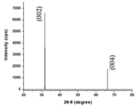
- FIG. 5 is a symmetrical X-ray diffraction diagram of a substrate with ⁇ -type gallium oxide nanorods.
- FIG. 1 is a schematic cross-sectional view showing an example of a substrate with ⁇ -type gallium oxide nanorods according to an embodiment of the present invention.
- FIG. 2 is a schematic configuration diagram showing an example of a manufacturing apparatus used for manufacturing a substrate with ⁇ -
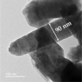
- FIG. 6 is a diagram showing a transmission electron microscope image of ⁇ -type gallium oxide nanorods on a substrate with ⁇ -type gallium oxide nanorods.
- FIG. 7 is a diagram showing a high-magnification transmission electron microscope image of ⁇ -type gallium oxide nanorods on a substrate with ⁇ -type gallium oxide nanorods.
- FIG. 8 shows an atomic force microscope (AFM) image and a reflection high-energy electron diffraction (RHEED) pattern of the surface of a ⁇ -type gallium oxide single crystal substrate with (001) plane orientation treated with oxygen radicals. be.
- AFM atomic force microscope
- RHEED reflection high-energy electron diffraction
- a single crystal substrate means a substrate whose entire substrate is a single crystal.
- oxygen constituent particles are oxygen atoms containing singlet oxygen atoms and triplet oxygen atoms, oxygen molecules, ozone, or particles containing these in an excited state.
- ⁇ indicating a numerical range is used to include the numerical values written before and after it as the lower limit and upper limit.
- a substrate with ⁇ -type gallium oxide nanorods has a substrate having a pair of main surfaces, and a plurality of ⁇ -type gallium oxide nanorods formed on at least one main surface of the substrate, The ⁇ -type gallium oxide nanorods are oriented perpendicularly to the main surface.
- the term " ⁇ -type gallium oxide nanorods vertically aligned" means that the longitudinal direction of the ⁇ -type gallium oxide nanorods is substantially perpendicular to a reference plane. Specifically, this means that the angle of the center line of the nanorod measured with a scanning electron microscope (SEM) is within 90 ⁇ 15° with respect to the main surface, and more preferably within 90 ⁇ 10°.
- FIG. 1 is a schematic cross-sectional view showing an example of a substrate 100 with ⁇ -type gallium oxide nanorods according to an embodiment of the present invention.
- the substrate 100 with ⁇ -type gallium oxide nanorods includes a substrate 110 and a plurality of ⁇ -type gallium oxide nanorods 120 formed on the substrate 110.
- ⁇ -type gallium oxide nanorods 120 are formed on the first main surface 110a of the substrate 110.
- the ⁇ -type gallium oxide nanorods 120 are oriented perpendicularly to the main surface 110a.
- the ⁇ -type gallium oxide nanorods 120 may be provided on at least one main surface of the substrate 110, that is, the first main surface 110a, and may be provided on both main surfaces. However, from the viewpoint of epitaxial growth of the ⁇ -type gallium oxide nanorods 120, the ⁇ -type gallium oxide nanorods 120 are preferably provided only on the first main surface 110a.
- the substrate 110 examples include, but are not limited to, a single crystal substrate, a polycrystalline substrate, a resin substrate, a glass substrate, and the like.
- the substrate 110 is preferably a single crystal substrate from the viewpoint of improving the crystallinity of the ⁇ -type gallium oxide nanorods.
- single crystal substrates include ⁇ -type gallium oxide single crystal substrates, silicon single crystal substrates, gallium nitride single crystal substrates, sapphire single crystal substrates, other oxide single crystal substrates, SiC single crystal substrates, etc. From the viewpoint of improving performance, a ⁇ -type gallium oxide single crystal substrate is preferable, and from the viewpoint of productivity, a silicon single crystal substrate, a sapphire single crystal substrate, or another oxide single crystal substrate is preferable.
- the oxide include MgO, MgAl 2 O 4 , SrTiO 3 , and ZrO 2 .
- ⁇ -type gallium oxide nanorods can be grown on a substrate.
- the ⁇ -type gallium oxide single crystal substrate conventionally known ones can be used, but for example, a substrate grown by crystal growth using the Czochralski method or the floating zone (FZ) method and then cut and polished is preferably used.
- the ⁇ -type gallium oxide single crystal substrate is more preferably a (001) plane-oriented substrate. Further, it is more preferable to form the ⁇ -type gallium oxide nanorods on the (001) plane-oriented main surface as the first main surface.
- resin substrates examples include polyethylene, polypropylene, polyvinyl chloride, polyvinylidene chloride, polystyrene, polyvinyl acetate, polytetrafluoroethylene, ABS (acrylonitrile butadiene styrene) resin, AS (acrylonitrile styrene) resin, and acrylic resin (polymethacrylate).
- thermoplastic resins such as methyl acid, etc.
- thermosetting resins such as phenol resins, epoxy resins, melamine resins, urea resins, unsaturated polyester resins, alkyd resins, polyurethanes, thermosetting polyimides, and silicone rubbers.
- the ⁇ -type gallium oxide nanorods 120 are nanorods formed, for example, by crystal growth, preferably epitaxial growth, of ⁇ -type gallium oxide on a substrate.
- the ⁇ -type gallium oxide nanorods 120 may be nanorods formed by epitaxially growing ⁇ -type gallium oxide on another substrate and transferred onto the substrate 110 by a method that will be exemplified later.
- a plurality of ⁇ -type gallium oxide nanorods 120 are formed on the first main surface 110a of the substrate 110, and are oriented perpendicularly to the first main surface 110a.
- the ⁇ -type gallium oxide nanorods may be single crystal or polycrystalline, but from the viewpoint of the yield and characteristics of semiconductor devices, a single crystal or a crystal close to a single crystal is preferable, and is composed of a single crystal. It is more preferable.
- a crystal close to a single crystal means that the entire nanorod consists of a single crystal with the same atomic arrangement.
- the ⁇ -type gallium oxide nanorods are preferably (001)-oriented single crystals. Note that when n-type or p-type ⁇ -type gallium oxide nanorods are formed by mixing a small amount of impurities, the ⁇ -type gallium oxide nanorods may contain these impurities.
- an index of its crystallinity includes the presence or absence of a peak of ⁇ -type gallium oxide attributed to the (001) plane by symmetric X-ray diffraction.
- a peak attributed to the (001) plane be observed by symmetrical X-ray diffraction.
- Examples of the peak of ⁇ -type gallium oxide attributed to the (001) plane include peaks of the (002) plane, (004) plane, and the like. This makes it possible to confirm the presence of a ⁇ -type gallium oxide nanorod single crystal in the ⁇ -type gallium oxide nanorods.
- symmetrical X-ray diffraction measurement for example, CuK ⁇ rays are used as a radiation source, the X-rays are irradiated onto the surface of the substrate at a Bragg diffraction angle ⁇ , and the diffracted X-rays are detected at a detector at ⁇ -2 ⁇ . Do it by rotating.
- a diffraction peak is obtained at .28°. Therefore, if a diffraction peak is obtained at the above-mentioned Bragg diffraction angle, it can be attributed to the peak of the (001) plane of ⁇ -type gallium oxide.
- the full width at half maximum (FWHM, Full Width Half Maximum) of the peak attributed to the (001) plane is 15 arcsec or more and 50 arcsec or less.
- the crystallinity of the ⁇ -type gallium oxide single crystal can be quantitatively evaluated based on the half-width of such a peak.
- the lower limit of the half-value width is not particularly limited, but, for example, the half-value width is preferably 15 arcsec or more, and more preferably 20 arcsec or more. Such half width can be measured by X-ray diffraction rocking curve measurement.
- substantially no dislocations exist in the ⁇ -type gallium oxide nanorods.
- the substantial absence of dislocations in the ⁇ -type gallium oxide nanorods can be confirmed by observing the ⁇ -type gallium oxide nanorods using a transmission electron microscope. Specifically, if 10 or more nanorods are observed using a transmission electron microscope and no dislocations are observed, it can be determined that there are substantially no dislocations in the ⁇ -type gallium oxide nanorods.
- the height of the ⁇ -type gallium oxide nanorods is preferably 0.5 ⁇ m or more and 50 ⁇ m or less.
- the height of the ⁇ -type gallium oxide nanorod is preferably 0.5 ⁇ m or more, more preferably 0.8 ⁇ m or more, and even more preferably 1 ⁇ m or more, since it is suitable for flowing a sample solution in biological device applications.
- the upper limit of the height of the ⁇ -type gallium oxide nanorods is not particularly limited, but from the viewpoint of productivity and ease of controlling the quality of the ⁇ -type gallium oxide nanorods, the height is preferably 50 ⁇ m or less.
- the height of the ⁇ -type gallium oxide nanorods may be, for example, 0.8 ⁇ m or more and 30 ⁇ m or less, or 1 ⁇ m or more and 20 ⁇ m or less.
- the height of the ⁇ -type gallium oxide nanorods can be determined, for example, by observing a cross section of the substrate with the ⁇ -type gallium oxide nanorods using a scanning electron microscope and measuring the length from the main surface of the substrate to the top of the nanorods. Note that it is preferable that the heights of 10 or more nanorods are measured and the average value thereof is within the above range.
- the thickness of the ⁇ -type gallium oxide nanorods is preferably 10 nm to 200 nm. From the viewpoint of strength, the thickness of the ⁇ -type gallium oxide nanorod is preferably 10 nm or more, more preferably 20 nm or more, even more preferably 30 nm or more, and even more preferably 40 nm or more. On the other hand, from the viewpoint of increasing the density, the thickness of the ⁇ -type gallium oxide nanorods is preferably 200 nm or less, more preferably 150 nm or less, even more preferably 120 nm or less, and even more preferably 100 nm or less.
- the thickness of the ⁇ -type gallium oxide nanorods can be determined, for example, by observing the ⁇ -type gallium oxide nanorods using a transmission electron microscope and measuring the diameter of the ⁇ -type gallium oxide nanorods. Note that it is preferable that the diameters of 10 or more nanorods are measured and the average value is within the above range.
- the density of ⁇ -type gallium oxide nanorods formed per 1 ⁇ m 2 of the main surface of the substrate is preferably 20 to 10,000 nanorods/ ⁇ m 2 .
- the density is preferably 20 lines/ ⁇ m 2 or more, more preferably 50 lines/ ⁇ m 2 or more, even more preferably 80 lines/ ⁇ m 2 or more, and more preferably 100 lines/ ⁇ m 2 or more from the viewpoint of biological device performance and light receiving/emitting device performance. More preferred.
- the density is preferably 10000 lines/ ⁇ m 2 or less, more preferably 1000 lines/ ⁇ m 2 or less, even more preferably 800 lines/ ⁇ m 2 or less, and more preferably 500 lines/ ⁇ m 2 or less from the viewpoint of the difficulty of device production. More preferred.
- the height of the ⁇ -type gallium oxide nanorods can be determined, for example, by observing the surface of the substrate with ⁇ -type gallium oxide nanorods using a scanning electron microscope and measuring the number of nanorods per unit area.
- ⁇ -type gallium oxide nanorods can be formed on a substrate without using a buffer layer. Therefore, a buffer layer may or may not be provided between the ⁇ -type gallium oxide nanorods and the substrate.
- the buffer layer is a layer inserted mainly for the purpose of alleviating lattice mismatch, and is a layer having a thickness of 20 nm or more, for example.
- a nucleation layer may be provided between the ⁇ -type gallium oxide nanorods and the substrate.
- the nucleation layer is a layer inserted for the purpose of promoting crystallization of ⁇ -type gallium oxide, and its thickness is, for example, less than 20 nm, preferably less than 10 nm, and more preferably less than 5 nm.
- the nucleation layer may be a continuous layer or a discontinuous layer. Examples of the nucleation layer include a layer containing an element different from that of the substrate, or a surface-modified layer formed by modifying the surface of the substrate.
- the above-mentioned buffer layer may be, for example, a single crystal film of the material with a predetermined thickness, a layer formed by gradually changing the composition of a mixed crystal of the material and a different material, or a superlattice structure of the material and a different material.
- the nucleation layer refers to a thin film or layer having a lattice constant different from that of the adsorption layer or the material in question.
- the surface modified layer is a layer obtained by modifying the surface of a substrate such as a single crystal substrate, and makes it easier for the nanorods to grow by matching the polarity with the nanorods.
- the presence of a nucleation layer can be determined from the difference in atomic arrangement observed by cross-sectional TEM (transmission electron microscope) observation.
- the substrate with ⁇ -type gallium oxide nanorods according to the embodiment of the present invention has the ⁇ -type gallium oxide nanorods oriented perpendicularly to at least one main surface of the substrate, so that the analyte solution can easily flow in the biological device. It has advantages such as easy formation of a pn junction structure in a light emitting device, and is highly applicable industrially, which is preferable.
- Such a substrate with ⁇ -type gallium oxide nanorods can be suitably used in various applications such as biosensors, biodevices such as biomolecule extraction devices, microchannel devices, ultraviolet light emitting/receiving elements, and radiation detectors.
- the present invention relates to a biomolecule extraction device having a substrate with ⁇ -type gallium oxide nanorods according to an embodiment of the present invention. That is, the biomolecule extraction device according to the embodiment of the present invention has the above-mentioned substrate with ⁇ -type gallium oxide nanorods, includes a microchannel formed on the substrate, and the ⁇ -type gallium oxide nanorods have the above-described ⁇ -type gallium oxide nanorods. It is formed within the microchannel.
- a biomolecule extraction device is a device that can extract biomolecules from a sample by flowing the sample through its microchannel.
- the biomolecules contained in the sample are adsorbed by the ⁇ -type gallium oxide nanorods formed within the microchannel, and the solution other than the adsorbed biomolecules passes through the microchannel. This separates biomolecules from the sample.
- a part of the microchannel or the nanorods may be charged depending on the type of biomolecule to be extracted. Examples of the charging method include applying an electric field to the microchannel, and forming a coating layer on the surface of the ⁇ -type gallium oxide nanorod.
- the microchannel formed on the substrate is not particularly limited as long as it functions as a channel for flowing a sample, but it may be a channel-shaped recess formed on at least one main surface of the substrate, for example. good.
- the depth and width of the microchannel are not particularly limited and can be adjusted depending on the target biomolecule; however, if the spatial volume of the microchannel is made too small, pressure loss tends to increase.
- the depth and width may each be 1 ⁇ m or more.
- a mechanism for introducing or collecting a sample may be provided at an end thereof, as a sample inputting part or a sample collecting part.
- the biomolecule extraction device is similar to the substrate with ⁇ -type gallium oxide nanorods according to the embodiment of the present invention, except that it includes ⁇ -type gallium oxide nanorods in the microchannel formed on the substrate.
- the method for forming ⁇ -type gallium oxide nanorods in a microchannel is not particularly limited. For example, by forming ⁇ -type gallium oxide nanorods on a substrate on which a microchannel has been formed in advance, ⁇ -type gallium oxide nanorods can be formed in a microchannel. Gallium oxide nanorods may also be formed. Further, the substrate with ⁇ -type gallium oxide nanorods on which ⁇ -type gallium oxide nanorods are formed may be processed so that the ⁇ -type gallium oxide nanorods are provided in the microchannel.
- a convex portion on the main surface of the substrate serving as a template. That is, a mold is formed by forming ⁇ -type gallium oxide nanorods on the convex portion, and a material of another substrate is applied and hardened on the main surface of the mold that includes the ⁇ -type gallium oxide nanorods (provided with the convex portion). It is preferable to form another substrate by a method such as.
- the substrate with ⁇ -type gallium oxide nanorods obtained by this method in which the ⁇ -type gallium oxide nanorods are transferred to another substrate, recesses corresponding to the protrusions of the mold are formed on the other substrate, and these are formed as microchannels. Become. Furthermore, since the ⁇ -type gallium oxide nanorods are transferred into the recesses, a biomolecule extraction device including the ⁇ -type gallium oxide nanorods in the microchannel can be obtained. According to this method, the ⁇ -type gallium oxide nanorods to be transferred are embedded in the recesses, and even if the sample inflow speed is increased, the nanowires are difficult to separate from the microchannel, which is preferable. Note that when the ⁇ -type gallium oxide nanorods are transferred by this method, the ⁇ -type gallium oxide nanorods may be grown again after the transfer.
- the above-mentioned resin substrate is suitably used as another substrate.
- a resin for the resin substrate that is light-transmissive and has no affinity with biomolecules.
- the material include cycloolefin polymer (COP), polydimethylsiloxane (PDMS), polymethyl methacrylate (PMMA), polycarbonate (PC), plastics such as hard polyethylene, and silicone.
- Samples used in biomolecule extraction devices include, for example, liquids containing biomolecules as described below, and specifically, culture fluids, body fluids such as serum and urine, and suspensions containing cells, viruses, bacteria, etc. Examples include liquids and the like.
- biomolecules that can be extracted by the biomolecule extraction device include exosomes containing microRNA, and nucleic acids contained in cells, viruses, bacteria, and the like.
- cells include those having a cell membrane structure, such as Staphylococcus, Bacillus subtilis, E. coli, Salmonella, Pseudomonas aeruginosa, Vibrio cholerae, Shigella, Bacillus anthrax, Mycobacterium tuberculosis, Clostridium botulinum, Clostridium tetani, Streptococcus, etc.
- bacteria granulocytes, lymphocytes, reticulocytes, red blood cells, white blood cells, blood cells such as platelets, and the like.
- viruses examples include norovirus, rotavirus, influenza virus, adenovirus, coronavirus, measles virus, rubella virus, hepatitis virus, herpes virus, and HIV.
- examples of the fungus include mushrooms, molds, and yeast, and specific examples include Trichophyton, Candida, Aspergillus, and Yeast.
- mitochondria and extracellular vesicles can also be cited as biomolecules.
- a method for manufacturing a substrate with ⁇ -type gallium oxide nanorods includes, for example, the following steps 1 to 4.
- Step 1 Step of installing a substrate inside the reaction chamber.
- Step 2 A step of turning a mixed gas containing oxygen and ozone into plasma, dissociating the ozone into oxygen constituent particles, and supplying the resulting particles to the reaction chamber under reduced pressure.
- Step 3 Along with Step 2, a step of supplying gallium element to the reaction chamber.
- Step 4 A step of epitaxially growing ⁇ -type gallium oxide nanorods on the substrate.
- the manufacturing apparatus 1000 includes a reaction chamber 1100, a substrate placement section 1200, a gallium element supply device 1300, an oxygen element supply device 1400, and a heating device 1220.
- the reaction chamber 1100 is a place where ⁇ -type gallium oxide nanorods are epitaxially grown on the substrate 110.
- the inside of the reaction chamber 1100 is equipped with a substrate placement section 1200 and a susceptor 1210, and the substrate 110 is placed in the substrate placement section 1200, and the substrate 110 is supported by the susceptor 1210.
- the substrate placement section 1200 in the reaction chamber 1100 can be heated by a heating device 1220, and the substrate 110 can be set to a desired temperature. It is preferable that the temperature of the substrate placement section 1200 be raised to 0° C. or higher, and preferably to room temperature or higher, using a heating device. Further, the upper limit of the heating temperature is not particularly limited, but it is sufficient if it can be heated to, for example, 700°C.
- a gallium element supply device 1300 supplies gallium element (Ga) to the placed substrate 110 .
- This gallium element supply device 1300 is not particularly limited as long as it can supply gallium element, but for example, a Knudsen cell can be mentioned.
- the gallium element supply device 1300 has a shutter 1310, which allows communication between the gallium element supply device 1300 and the reaction chamber 1100 to be made or shut off.
- the gallium element supply device 1300 may include a heating device and a cooling device.
- oxygen constituent particles are supplied to the arranged substrate 110 by an oxygen element supply device 1400.
- This oxygen element supply device 1400 includes a plasma generation section 1450 and, if necessary, a shutter 1410.
- the shutter 1410 allows the oxygen element supply device 1400 and the reaction chamber 1100 to communicate with each other or disconnects them from each other.
- the oxygen element supply device 1400 may include a heating device and a cooling device.
- the oxygen constituent particles supplied to the substrate 110 by the oxygen element supply device 1400 are obtained by converting a mixed gas containing oxygen and ozone into plasma by the plasma generation unit 1450, and dissociating ozone.
- oxygen gas is supplied from the oxygen gas supply unit 1500 toward the oxygen element supply device 1400.
- Oxygen gas passes through an oxygen gas supply pipe 1810 and flows into the ozonizer 1700 while its flow rate is adjusted by a mass flow controller 1820.
- a portion of the oxygen gas that has flowed into the ozonizer 1700 is converted into ozone, resulting in a mixed gas containing oxygen and ozone.
- An example of such an ozonizer 1700 is a first plasma generator that turns oxygen gas into plasma.
- the ozonizer 1700 preferably has the ability to increase the concentration of ozone to the total of oxygen and ozone to 10% by volume or more, more preferably 20% by volume or more, and even more preferably 25% by volume or more. .
- the mixed gas containing oxygen and ozone generated by the ozonizer 1700 passes through the ozone/oxygen mixed gas supply pipe 1830 and flows into the oxygen element supply device 1400 while the flow rate is adjusted by the mass flow controller 1840.
- the ozonizer 1700 and the oxygen element supply device 1400 may be directly connected, and in that case, the ozone-oxygen mixed gas supply pipe 1830 and the mass flow controller 1840 are unnecessary.
- an inert gas is supplied to the oxygen element supply device 1400 from an inert gas supply section 1600.
- the inert gas include rare gases such as Ar gas and He gas.
- the supply of the inert gas is optional.
- the inert gas passes through the inert gas supply pipe 1850 from the inert gas supply section 1600 and flows into the oxygen element supply device 1400 while the flow rate is adjusted by the mass flow controller 1860.
- the mixed gas containing oxygen and ozone and the inert gas may flow into the oxygen element supply device 1400 separately, but as shown in FIG. may be supplied to the oxygen element supply device 1400 in a mixed state.
- the mixed gas supply pipe 1870 is a pipe for supplying a mixed gas containing oxygen and ozone and an inert gas for generating plasma to the oxygen element supply device 1400.
- the inert gas supply section 1600, inert gas supply pipe 1850, and mass flow controller 1860 are unnecessary.
- the manufacturing apparatus 1000 may include an impurity element supply unit (not shown) that supplies impurities.
- the impurity element supply section supplies an impurity element to grow n-type gallium oxide or p-type gallium oxide.
- the impurity element supply section may be, for example, a Knudsen cell; in this case, the Knudsen cell is heated to evaporate, for example, Si or Sn in the case of an n-type, and Mg in the case of a p-type, and the evaporated gas is supplied to the reaction chamber 1100. do. As a result, ⁇ -type gallium oxide doped with these impurity elements can be grown.
- Step 1 the substrate 110 is installed inside the reaction chamber 1100. That is, the substrate 110 is placed on the substrate placement section 1200 and supported by the susceptor 1210. Then, the substrate placement section 1200 is heated using the heating device 1220 to heat the substrate 110 to a desired temperature, and the reaction chamber 1100 is depressurized in preparation for the subsequent step 2. Note that the internal pressure of the reaction chamber 1100 and the temperature of the substrate placement part 1200, that is, the temperature of the substrate 110, are preferably set to the internal pressure and temperature described in (Step 4) described later.
- the various substrates mentioned above can be suitably used.
- a nucleation layer may be formed on the surface of the substrate 110, or ⁇ -type gallium oxide nanorods may be directly formed on the surface of the substrate 110. Formation of the nucleation layer facilitates the growth of ⁇ -type gallium oxide nanorods.
- a method of performing oxygen plasma treatment on the surface of the substrate 110 can be used. Oxygen plasma treatment is a surface treatment in which a mixed gas containing oxygen and ozone is turned into plasma, and the ozone is dissociated into oxygen constituent particles.
- a nucleation layer made of a different material may be formed on the surface of the substrate 110. Examples of the different materials in this case include SiO 2 , Si 3 N 4 , Al 2 O 3 , In 2 O 3 , AlN, GaN, and InN.
- Step 2 a mixed gas containing oxygen and ozone is turned into plasma, and the ozone is dissociated into oxygen constituent particles, which are then supplied to the reaction chamber 1100 under reduced pressure. Specifically, as described above, a part of the oxygen gas supplied from the oxygen gas supply section 1500 to the ozonizer 1700 is plasma-treated by the first plasma generated by the ozonizer 1700 and becomes ozone. A mixed gas containing ozone and ozone is obtained. This is supplied to the oxygen element supply device 1400 via the mixed gas supply pipe 1870.
- the ozonizer 1700 adjusts the concentration of ozone to the total of oxygen and ozone to 10% by volume or more, more preferably 20% by volume or more, and still more preferably 25% by volume or more.
- the upper limit of the ozone concentration is not particularly limited, but is usually 50% by volume or less.
- an inert gas such as Ar gas is supplied from the inert gas supply unit 1600 to the oxygen element supply device 1400 via the mixed gas supply pipe 1870.
- the mixed gas containing oxygen and ozone and the inert gas are mixed inside the mixed gas supply pipe 1870 to form a mixed gas containing oxygen, ozone, and the inert gas.
- the mixing ratio of the mixed gas containing oxygen and ozone and the inert gas is 100 parts by volume of the mixed gas containing oxygen and ozone, and the ratio of the inert gas is 350 parts by volume from the viewpoint of plasma ignition. It is preferably at least 400 parts by volume, more preferably at least 400 parts by volume. Further, from the viewpoint of the density of oxygen radicals, the proportion of the inert gas is preferably 1900 parts by volume or less, more preferably 1500 parts by volume or less, even more preferably 1000 parts by volume or less, and even more preferably 460 parts by volume or less. That is, the proportion of the inert gas is preferably 350 parts by volume to 1900 parts by volume, more preferably 400 parts to 1500 parts by volume, even more preferably 400 parts to 1000 parts by volume, even more preferably 400 parts to 460 parts by volume. preferable.
- oxygen radicals with strong oxidizing power containing a large amount of singlet oxygen atoms O( 1 D) are thought to be generated.
- the oxygen radicals include singlet oxygen atoms O( 1 D) and triplet oxygen atoms O( 3 P). Singlet oxygen atoms O( 1 D) transition to triplet oxygen atoms O( 3 P) at a predetermined rate.
- Ozone dissociated into oxygen molecules and oxygen radicals in this manner is referred to as oxygen constituent particles, and is supplied to the reaction chamber 1100 under reduced pressure. Note that this does not preclude that not only the oxygen constituent particles but also a mixed gas containing non-plasmaized oxygen and ozone may be supplied to the reaction chamber 1100 under reduced pressure.
- step 3 gallium element is supplied to the reaction chamber 1100 under reduced pressure. That is, gallium element (Ga) is supplied from the gallium element supply device 1300 to the reaction chamber 1100 under reduced pressure. As a result, the supplied Ga reacts with the oxygen radicals provided in step 2 on the surface of the substrate 110, and ⁇ -type gallium oxide nanorods are generated on the surface of the substrate 110. Specifically, near the surface of the substrate 110, Ga reacts with singlet oxygen atoms O( 1 D) or triplet oxygen atoms O( 3 P) to which singlet oxygen atoms O( 1 D) have transitioned. , ⁇ -type gallium oxide nanorods grow.
- the gas pressure supplied from the oxygen element supply device 1400 containing oxygen constituent particles in step 2 is preferably 1.0 ⁇ 10 ⁇ 5 Pa or higher, and 1.0 ⁇ 10 ⁇ 4 Pa from the viewpoint of supplying sufficient oxygen radicals.
- the pressure is more preferably 1.0 ⁇ 10 ⁇ 3 Pa or more, and even more preferably 1.0 ⁇ 10 ⁇ 3 Pa or more.
- the gas pressure supplied from the oxygen element supply device 1400 containing oxygen constituent particles in step 2 is preferably 1.0 ⁇ 10 ⁇ 1 Pa or less, and 1.0 ⁇ 10 ⁇ 2 More preferably, it is less than Pa.
- the gas pressure supplied from the oxygen element supply device 1400 is preferably 1.0 ⁇ 10 ⁇ 5 Pa to 1.0 ⁇ 10 ⁇ 1 Pa, and preferably 1.0 ⁇ 10 ⁇ 4 Pa to 1.0 ⁇ 10 ⁇ 1 Pa is more preferable, and 1.0 ⁇ 10 ⁇ 3 Pa to 1.0 ⁇ 10 ⁇ 2 Pa is even more preferable.
- the gas pressure supplied from the gallium element supply device 1300 in step 3 is preferably 1.0 ⁇ 10 -8 Pa or more, more preferably 1.0 ⁇ 10 -7 Pa or more, from the viewpoint of supplying sufficient Ga element. More preferably, it is 1.0 ⁇ 10 ⁇ 6 Pa or more.
- the gas pressure supplied from the gallium element supply device 1300 is high and the amount of Ga element supplied is too large, it becomes thermodynamically difficult to grow ⁇ -type gallium oxide. is preferably 1.0 ⁇ 10 ⁇ 2 Pa or less, more preferably 1.0 ⁇ 10 ⁇ 3 Pa or less.
- the gas pressure supplied from the gallium element supply device 1300 is preferably 1.0 ⁇ 10 ⁇ 8 Pa to 1.0 ⁇ 10 ⁇ 2 Pa, and 1.0 ⁇ 10 ⁇ 7 Pa to 1.0 ⁇ 10 ⁇ 3 Pa is more preferable, and 1.0 ⁇ 10 ⁇ 6 Pa to 1.0 ⁇ 10 ⁇ 3 Pa is even more preferable.
- Step 4 is a step in which ⁇ -type gallium oxide is epitaxially grown on the substrate 110 by the steps 2 and 3 described above.
- the internal pressure of the reaction chamber 1100 is preferably 0.005 Pa or more, more preferably 0.01 Pa or more, from the viewpoint of the exhaust capacity of the apparatus. Further, from the viewpoint of the mean free path of oxygen radicals and gallium, the internal pressure is preferably 0.1 Pa or less, more preferably 0.05 Pa or less. That is, the internal pressure of the reaction chamber 1100 is preferably 0.005 Pa to 0.1 Pa, more preferably 0.01 Pa to 0.05 Pa.
- the temperature of the substrate 110 is preferably 200° C. or higher, more preferably 250° C. or higher, and even more preferably 300° C. or higher, from the viewpoint of crystal growth. Further, from the viewpoint of growth rate, the growth temperature is preferably 500°C or lower, more preferably 400°C or lower. That is, the growth temperature is preferably 200°C to 500°C, more preferably 250°C to 400°C, even more preferably 3000°C to 400°C. Note that the growth temperature is defined, for example, as a set temperature in the heating device 1220.
- the plasma output is preferably 300 W or more, more preferably 350 W or more, and even more preferably 400 W or more.
- the plasma output is preferably 800 W or less, more preferably 750 W or less, and even more preferably 700 W or less.
- the mixed gas in step 3 is supplied to the reaction chamber at a flow rate of 0.2 sccm to 1.0 sccm. It is preferable. From the viewpoint of the amount of oxygen radicals required to generate ⁇ -type gallium oxide, the flow rate is preferably 0.2 sccm or more, more preferably 0.4 sccm or more, and even more preferably 0.6 sccm or more.
- the flow rate is preferably 1.0 sccm or less, more preferably 0.95 sccm or less, and even more preferably 0.90 sccm or less.
- both the plasma output and the flow rate of the mixed gas are within the above ranges.
- Methods for making the ⁇ -type gallium oxide nanorods relatively thick include, for example, increasing the gas pressure supplied from the gallium element supply device, decreasing the supply amount of a mixed gas containing oxygen and ozone, etc. can be mentioned.
- methods for increasing the length of the ⁇ -type gallium oxide nanorods include relatively increasing the growth rate of the ⁇ -type gallium oxide nanorods, increasing the time for crystal growth, and the like.
- Methods for relatively increasing the growth rate of ⁇ -type gallium oxide nanorods include, for example, increasing the gas pressure supplied from the gallium element supply device, increasing the supply amount of a mixed gas containing oxygen and ozone, etc. Can be mentioned.
- Methods for relatively increasing the density of ⁇ -type gallium oxide nanorods include, for example, increasing the growth rate of ⁇ -type gallium oxide nanorods, increasing the supply amount of a mixed gas containing oxygen and ozone, and supplying gallium element. Examples include lowering the gas pressure supplied from the device.
- a substrate with ⁇ -type gallium oxide nanorods according to an embodiment of the present invention can be obtained. According to this method, not only can a substrate with ⁇ -type gallium oxide nanorods having the above-mentioned characteristics be obtained, but also the growth rate in the epitaxial growth of ⁇ -type gallium oxide is fast and a low growth temperature can be used, resulting in excellent productivity.
- ⁇ -type gallium oxide nanorods can be attached to the substrate without requiring a buffer layer. be made to grow upwards.
- a substrate with ⁇ -type gallium oxide nanorods including ⁇ -type gallium oxide nanorods with excellent crystallinity can be obtained.
- a substrate with ⁇ -type gallium oxide nanorods having excellent crystallinity is highly applicable industrially and is preferred.
- ⁇ -type gallium oxide nanorods according to an embodiment of the present invention can be obtained by using a substrate with ⁇ -type gallium oxide nanorods obtained by the above method as a template, and transferring ⁇ -type gallium oxide nanorods included in the template to another substrate. It may also be manufactured by As a method for transferring the ⁇ -type gallium oxide nanorods to another substrate, for example, another substrate is formed by applying and curing the material of another substrate on the surface of the template having the ⁇ -type gallium oxide nanorods. There is a method of transferring the ⁇ -type gallium oxide nanorods onto another substrate by then peeling off the substrate provided in the template.
- the ⁇ -type gallium oxide nanorods may be grown again on another substrate.
- the above-mentioned resin substrate is preferably used, for example.
- the ⁇ -type gallium oxide nanorods included in the template are oriented perpendicularly to the main surface of the substrate, so that they can be oriented perpendicularly to the main surface of another substrate. ⁇ -type gallium oxide nanorods can be obtained.
- ⁇ -type gallium oxide nanorods were epitaxially grown on a ⁇ -type gallium oxide single crystal substrate according to the following procedure to obtain a substrate with ⁇ -type gallium oxide nanorods.
- a ⁇ -type gallium oxide single crystal substrate whose bulk was oriented in the (001) plane was washed with an organic solvent, then washed with an acid, and dried. Thereafter, a ⁇ -type gallium oxide single crystal substrate was placed on the substrate placement section 1200 so that the (001) plane was the surface, and supported by a susceptor 1210. Thereafter, oxygen plasma treatment was performed for 15 minutes under the following conditions.
- Plasma output 600W
- Gas used Ar and mixed gas (O 2 + O 3 )
- Ar flow rate 3.2 sccm
- O2 + O3 flow rate 0.8sccm
- Reaction chamber pressure 6.0 ⁇ 10 ⁇ 5 Torr (8.0 ⁇ 10 ⁇ 3 Pa)
- Substrate temperature set temperature of heating device: 300°C
- the substrate temperature (set temperature of the heating device) was subsequently set to 300° C., and the gas pressure supplied from the gallium element supply device 1300 was set to 8.5 ⁇ 10 ⁇ 7 Torr (1.1 ⁇ 10 ⁇ 4 Pa).
- gallium oxide was epitaxially grown for 60 minutes to obtain a substrate with ⁇ -type gallium oxide nanorods. Note that the pressure inside the reaction chamber during growth was 6.0 ⁇ 10 ⁇ 5 Torr (8.0 ⁇ 10 ⁇ 3 Pa).
- FIG. 3 is a scanning electron micrograph showing the surface of the obtained substrate with ⁇ -type gallium oxide nanorods.
- FIG. 3(a) is a scanning electron micrograph at a magnification of 20,000 times
- FIG. 3(b) is a scanning electron micrograph at a magnification of 50,000 times.
- FIG. 4 is a scanning electron micrograph showing a cross section of the obtained substrate with ⁇ -type gallium oxide nanorods, and the photographing magnification is 20,000 times.
- FIGS. 3 and 4 it was confirmed that the growth on the ⁇ -type gallium oxide single crystal substrate ( ⁇ -type gallium oxide nanorods) had a very beautiful nanorod shape.
- the ⁇ -type gallium oxide nanorods were oriented perpendicularly to the main surface of the ⁇ -type gallium oxide single crystal substrate on which the ⁇ -type gallium oxide nanorods were formed.
- the height of the ⁇ -type gallium oxide nanorods was 1.6 ⁇ m.
- the thickness of the ⁇ -type gallium oxide nanorods was 90 nm.
- the density of ⁇ -type gallium oxide nanorods was about 40/ ⁇ m 2 per 1 ⁇ m 2 of the main surface of the ⁇ -type gallium oxide single crystal substrate.
- the growth rate of the ⁇ -type gallium oxide nanorods was 26.7 nm/min (1.6 ⁇ m/hour).
- ⁇ -type gallium oxide nanorods could be formed at a very fast growth rate on the (001) plane of the ⁇ -type gallium oxide single crystal substrate. Furthermore, the formed ⁇ -type gallium oxide nanorods are columnar, substantially perpendicular to the main surface, and have a relatively uniform diameter, which is very good. Furthermore, the growth temperature is extremely low at 300°C. Conventionally, it has been possible to form ⁇ -type gallium oxide nanorods in a beautiful shape that are oriented perpendicular to the plane formed on the substrate.
- ⁇ -type gallium oxide nanorods composed of Furthermore, it can be said that there is no example in which ⁇ -type gallium oxide nanorods composed of single crystals could be formed at a relatively high growth rate and at a relatively low temperature as in this example.
- a plurality of ⁇ -type gallium oxide nanorods are provided on at least one main surface of a substrate, and the ⁇ -type gallium oxide nanorods are oriented perpendicularly to the main surface. This is the first time that a printed circuit board has been provided, and the effects of the present invention are obvious.
- FIG. 5 is a symmetrical X-ray diffraction diagram of the obtained substrate with ⁇ -type gallium oxide nanorods. The horizontal axis in FIG. 5 is 2 ⁇ - ⁇ , and the vertical axis is intensity.
- FIG. 6 is a diagram showing a transmission electron microscope image of ⁇ -type gallium oxide nanorods on a substrate with ⁇ -type gallium oxide nanorods, and the observation magnification is 250,000 times.
- FIG. 7 is a diagram showing a high-magnification transmission electron microscope image of ⁇ -type gallium oxide nanorods on a substrate with ⁇ -type gallium oxide nanorods, and the observation magnification is 600,000 times.
- FIGS. 7(a) and 7(b) are diagrams showing the arrangement of the atomic planes of ⁇ -type gallium oxide nanorods at different observation positions, respectively.
- FIG. 8 shows an atomic force microscope (AFM) image and a reflection high-speed electron diffraction (RHEED) pattern of the surface of a ⁇ -type gallium oxide single crystal substrate with (001) plane orientation treated with oxygen radicals. It is a diagram.
- FIG. 8(a) is a diagram showing an atomic force microscope (AFM) image
- FIG. 8(b) is a diagram showing a reflection high-speed electron diffraction (RHEED) pattern. From FIG. 8, it was confirmed that the surface condition of the ⁇ -type gallium oxide single crystal substrate before growing ⁇ -type gallium oxide was good due to the surface treatment with oxygen radicals.
- the ⁇ -type gallium oxide single-crystal nanorods grown on the (001)-oriented ⁇ -type gallium oxide single-crystal substrate by the above method were (001)-oriented single crystals. According to the present invention, it is possible to produce ⁇ -type gallium oxide single crystal nanorods that are nearly perfect crystals with almost no dislocations, and therefore have high industrial applicability.
- a substrate having a pair of main surfaces, and a plurality of ⁇ -type gallium oxide nanorods formed on at least one main surface of the substrate, A substrate with ⁇ -type gallium oxide nanorods, wherein the ⁇ -type gallium oxide nanorods are oriented perpendicularly to the main surface.
- 3. The substrate with ⁇ -type gallium oxide nanorods according to 1 or 2 above, wherein the substrate is a single crystal substrate. 4. 4.
- 9. The substrate with ⁇ -type gallium oxide nanorods according to any one of 1 to 8 above, wherein the ⁇ -type gallium oxide nanorods have a thickness of 10 nm to 200 nm. 10.
- a method for manufacturing a substrate with ⁇ -type gallium oxide nanorods the method comprising epitaxially growing a plurality of ⁇ -type gallium oxide nanorods on the substrate. 13. 13. The method for manufacturing a substrate with ⁇ -type gallium oxide nanorods as described in 12 above, wherein the plasma generation is performed at a plasma output of 300W to 800W. 14. 14.
- Substrate 110 with ⁇ -type gallium oxide nanorods Substrate 110a First main surface 120 ⁇ -type gallium oxide nanorods 1000 Manufacturing device 1100 Reaction chamber 1200 Substrate placement section 1210 Susceptor 1220 Heating device 1300 Gallium element supply device 1310, 1410 Shutter 1400 Oxygen element supply device 1450 Plasma generation section 1500 Oxygen gas supply section 1600 Inert gas supply section 1700 Ozonizer 1810 Oxygen gas supply pipe 1820, 1840, 1860 Mass flow controller 1830 Ozone oxygen mixed gas supply pipe 1850 Inert gas supply pipe 1870 Mixed gas supply pipe
Abstract
The present invention pertains to a substrate with β-type gallium oxide nano rods that includes: a substrate having a pair of main surfaces; and a plurality of β-type gallium oxide nano rods which are formed on the substrate. The β-type gallium oxide nano rods are arrayed so as to be perpendicular to at least one of the main surfaces of the substrate.
Description
本明細書は、β型酸化ガリウムナノロッド付き基板及びその製造方法並びに生体分子抽出用デバイスに関する。
The present specification relates to a substrate with β-type gallium oxide nanorods, a method for manufacturing the same, and a device for extracting biomolecules.
酸化ガリウム(Ga2O3)は、α型、β型、γ型、δ型、ε型と種々の結晶構造をとる。これらのうちβ型酸化ガリウム(β型Ga2O3)は低温常圧において安定相である。β型酸化ガリウムの結晶系は単斜晶であり、格子定数は、a軸、すなわち[100]軸が12.214Å、b軸、すなわち[010]軸が3.0371Å、c軸、すなわち[001]軸が5.7981Åであり、a軸とc軸間の角度(β)が103.83°であることが知られている。β型酸化ガリウムのバンドギャップは4.5eVから4.9eV程度であり、4H-SiC基板のバンドギャップ3.26eVやGaNのバンドギャップ3.39eVよりも大きい。このため、β型酸化ガリウムは、高い絶縁破壊強度を備える半導体材料として期待されている。
Gallium oxide (Ga 2 O 3 ) has various crystal structures including α type, β type, γ type, δ type, and ε type. Among these, β-type gallium oxide (β-type Ga 2 O 3 ) is a stable phase at low temperature and normal pressure. The crystal system of β-type gallium oxide is monoclinic, and the lattice constants are 12.214 Å for the a-axis, that is, the [100] axis, 3.0371 Å for the b-axis, that is, the [010] axis, and 3.0371 Å for the c-axis, that is, the [001 ] axis is 5.7981 Å, and the angle (β) between the a-axis and c-axis is 103.83°. The band gap of β-type gallium oxide is about 4.5 eV to 4.9 eV, which is larger than the band gap of 3.26 eV of a 4H-SiC substrate and the band gap of 3.39 eV of GaN. Therefore, β-type gallium oxide is expected to be a semiconductor material with high dielectric breakdown strength.
例えば、特許文献1には、真空槽の内部に第1のセルからガリウム元素をβ型酸化ガリウム基板に供給し、オゾンを含む酸素ガスをβ型酸化ガリウム基板に供給することにより、β型酸化ガリウム単結晶膜を成長させる技術が開示されている。また、非特許文献1には、β型酸化ガリウムを成長させるために分子線エピタキシー(MBE)装置を用い、その際に酸素ガスをrf-プラズマにより処理する技術が開示されている。
For example, Patent Document 1 discloses that gallium element is supplied from a first cell inside a vacuum chamber to a β-type gallium oxide substrate, and oxygen gas containing ozone is supplied to the β-type gallium oxide substrate. Techniques for growing gallium single crystal films are disclosed. Furthermore, Non-Patent Document 1 discloses a technique in which a molecular beam epitaxy (MBE) apparatus is used to grow β-type gallium oxide, and at that time, oxygen gas is treated with RF-plasma.
また、半導体材料等の各種材料をナノロッドやナノワイヤの形態として、バイオデバイスや受発光素子といった種々のデバイスに応用することが検討されている。例えば特許文献2には、ZnOナノワイヤを生体分子の抽出用チップに用いることが記載されている。
In addition, consideration is being given to applying various materials such as semiconductor materials in the form of nanorods and nanowires to various devices such as biodevices and light-receiving/receiving elements. For example, Patent Document 2 describes the use of ZnO nanowires as a chip for extracting biomolecules.
特許文献1に記載の方法は、酸化ガリウム膜の成長温度が700℃以上と比較的高く、成長速度も約0.1μm/hと比較的遅い。また、特許文献1に記載の方法で得られる酸化ガリウムは、結晶性の点でも劣る。
In the method described in Patent Document 1, the growth temperature of the gallium oxide film is relatively high at 700° C. or higher, and the growth rate is also relatively slow at about 0.1 μm/h. Further, gallium oxide obtained by the method described in Patent Document 1 is also inferior in terms of crystallinity.
上記のように、酸化ガリウムに関しては半導体材料の成長技術が未熟であり、良い成長技術が見出されていない。とりわけ、基板の主面に対し垂直配向した形態のナノロッドに関して、β型酸化ガリウムから構成されるものを基板上に成長させた例は未だ知られていない。なお、ナノロッドやナノワイヤの形態や形状は様々であり得るが、例えばナノロッドやナノワイヤが基板の主面に対して垂直配向している場合、生体デバイスなどに応用する際に被検体溶液が流しやすい、受発光素子においてpn接合構造が作りやすい等の利点があり、工業的に応用性が高い。
As mentioned above, the growth technology for semiconductor materials for gallium oxide is immature, and no good growth technology has been found. In particular, with regard to nanorods oriented perpendicularly to the main surface of the substrate, there is no known example in which nanorods made of β-type gallium oxide are grown on a substrate. Note that nanorods and nanowires can have various forms and shapes, but for example, when nanorods and nanowires are oriented perpendicular to the main surface of the substrate, the analyte solution can flow easily when applied to biological devices. It has the advantage of being easy to form a pn junction structure in light receiving and emitting elements, and has high industrial applicability.
そこで本発明は、基板の主面に対し垂直配向した形態のβ型酸化ガリウムナノロッドを備える、新規なβ型酸化ガリウムナノロッド付き基板及びその製造方法を提供することを目的とする。また本発明は、上記β型酸化ガリウムナノロッド付き基板を用いた生体分子抽出用デバイスを提供することを目的とする。
Therefore, an object of the present invention is to provide a novel substrate with β-type gallium oxide nanorods, which includes β-type gallium oxide nanorods aligned perpendicularly to the main surface of the substrate, and a method for manufacturing the same. Another object of the present invention is to provide a biomolecule extraction device using the substrate with β-type gallium oxide nanorods.
本発明は、以下の1~17に関する。
1.一対の主面を有する基板と、前記基板の少なくとも一方の主面上に形成された複数のβ型酸化ガリウムナノロッドとを有し、
前記β型酸化ガリウムナノロッドは前記主面に対し垂直配向している、β型酸化ガリウムナノロッド付き基板。
2.前記β型酸化ガリウムナノロッドはβ型酸化ガリウムの単結晶で構成される、前記1に記載のβ型酸化ガリウムナノロッド付き基板。
3.前記基板は単結晶基板である、前記1に記載のβ型酸化ガリウムナノロッド付き基板。
4.前記基板はβ型酸化ガリウムの単結晶基板である、前記1に記載のβ型酸化ガリウムナノロッド付き基板。
5.対称X線回折により(001)面に帰属されるピークが観察される、前記1に記載のβ型酸化ガリウムナノロッド付き基板。
6.前記(001)面に帰属されるピークの半値幅が15arcsec以上50arcsec以下である、前記5に記載のβ型酸化ガリウムナノロッド付き基板。
7.前記β型酸化ガリウムナノロッド内に転位が実質的に存在しない、前記1に記載のβ型酸化ガリウムナノロッド付き基板。
8.前記β型酸化ガリウムナノロッドの高さが0.5μm以上50μm以下である、前記1に記載のβ型酸化ガリウムナノロッド付き基板。
9.前記β型酸化ガリウムナノロッドの太さが10nm~200nmである、前記1に記載のβ型酸化ガリウムナノロッド付き基板。
10.前記基板の前記主面1μm2あたりに形成された前記β型酸化ガリウムナノロッドの密度が20~10000本/μm2である、前記1に記載のβ型酸化ガリウムナノロッド付き基板。
11.前記1~10のいずれか1に記載のβ型酸化ガリウムナノロッド付き基板を有する生体分子抽出用デバイスであって、
前記基板上に形成されたマイクロ流路を備え、前記β型酸化ガリウムナノロッドは前記マイクロ流路内に形成されている、生体分子抽出用デバイス。
12.反応室の内部に基板を設置し、
酸素とオゾンとを含む混合ガスをプラズマ化して前記オゾンを酸素構成粒子に解離させ、減圧下の反応室に供給するとともに、
ガリウム元素を前記反応室に供給し、
前記基板の上に複数のβ型酸化ガリウムのナノロッドをエピタキシャル成長させることを含む、β型酸化ガリウムナノロッド付き基板の製造方法。
13.前記プラズマ化をプラズマ出力300W~800Wで行う、前記12に記載のβ型酸化ガリウムナノロッド付き基板の製造方法。
14.前記混合ガスを流量0.2sccm~1.0sccmで前記反応室に供給する、前記12又は13に記載のβ型酸化ガリウムナノロッド付き基板の製造方法。
15.前記基板の表面に対し酸素プラズマ処理を行い、その後、前記複数のβ型酸化ガリウムのナノロッドをエピタキシャル成長させる、前記12又は13に記載のβ型酸化ガリウムナノロッド付き基板の製造方法。
16.前記複数のβ型酸化ガリウムのナノロッドをエピタキシャル成長させる際の成長温度が200℃以上500℃以下である、前記12又は13に記載のβ型酸化ガリウムナノロッド付き基板の製造方法。
17.前記混合ガスの、前記酸素と前記オゾンとの合計に対する前記オゾンの濃度を10体積%以上とする、前記12又は13に記載のβ型酸化ガリウムナノロッド付き基板の製造方法。 The present invention relates to the following 1 to 17.
1. a substrate having a pair of main surfaces, and a plurality of β-type gallium oxide nanorods formed on at least one main surface of the substrate,
A substrate with β-type gallium oxide nanorods, wherein the β-type gallium oxide nanorods are oriented perpendicularly to the main surface.
2. 2. The substrate with β-type gallium oxide nanorods according to 1 above, wherein the β-type gallium oxide nanorods are composed of a single crystal of β-type gallium oxide.
3. 2. The substrate with β-type gallium oxide nanorods according to 1 above, wherein the substrate is a single crystal substrate.
4. 2. The substrate with β-type gallium oxide nanorods according to 1 above, wherein the substrate is a single-crystal substrate of β-type gallium oxide.
5. 2. The substrate with β-type gallium oxide nanorods according to 1 above, in which a peak attributed to the (001) plane is observed by symmetric X-ray diffraction.
6. 5. The substrate with β-type gallium oxide nanorods according to 5 above, wherein the half width of the peak attributed to the (001) plane is 15 arcsec or more and 50 arcsec or less.
7. 2. The substrate with β-type gallium oxide nanorods according to 1 above, wherein substantially no dislocations exist in the β-type gallium oxide nanorods.
8. 2. The substrate with β-type gallium oxide nanorods according to 1 above, wherein the β-type gallium oxide nanorods have a height of 0.5 μm or more and 50 μm or less.
9. 2. The substrate with β-type gallium oxide nanorods according to 1 above, wherein the β-type gallium oxide nanorods have a thickness of 10 nm to 200 nm.
10. 2. The substrate with β-type gallium oxide nanorods according to 1, wherein the density of the β-type gallium oxide nanorods formed per 1 μm 2 of the main surface of the substrate is 20 to 10,000 pieces/μm 2 .
11. A biomolecule extraction device having a substrate with β-type gallium oxide nanorods according to any one of 1 to 10 above,
A device for extracting biomolecules, comprising a microchannel formed on the substrate, and the β-type gallium oxide nanorods are formed within the microchannel.
12. Place the substrate inside the reaction chamber,
Converting a mixed gas containing oxygen and ozone into plasma to dissociate the ozone into oxygen constituent particles, supplying the mixture to a reaction chamber under reduced pressure,
supplying elemental gallium to the reaction chamber;
A method for manufacturing a substrate with β-type gallium oxide nanorods, the method comprising epitaxially growing a plurality of β-type gallium oxide nanorods on the substrate.
13. 13. The method for manufacturing a substrate with β-type gallium oxide nanorods as described in 12 above, wherein the plasma generation is performed at a plasma output of 300W to 800W.
14. 14. The method for producing a substrate with β-type gallium oxide nanorods as described in 12 or 13 above, wherein the mixed gas is supplied to the reaction chamber at a flow rate of 0.2 sccm to 1.0 sccm.
15. 14. The method for manufacturing a substrate with β-type gallium oxide nanorods as described in 12 or 13 above, wherein the surface of the substrate is subjected to oxygen plasma treatment, and then the plurality of β-type gallium oxide nanorods are epitaxially grown.
16. 14. The method for manufacturing a substrate with β-type gallium oxide nanorods according to 12 or 13 above, wherein the growth temperature when epitaxially growing the plurality of β-type gallium oxide nanorods is 200° C. or higher and 500° C. or lower.
17. 14. The method for manufacturing a substrate with β-type gallium oxide nanorods as described in 12 or 13 above, wherein the concentration of the ozone with respect to the total of the oxygen and the ozone in the mixed gas is 10% by volume or more.
本発明は、基板の少なくとも一方の主面に複数のβ型酸化ガリウムナノロッドを備え、当該β型酸化ガリウムナノロッドが上記主面に対し垂直配向しているβ型酸化ガリウムナノロッド付き基板を初めて提供するものである。
本発明に係るβ型酸化ガリウムナノロッド付き基板の製造方法は、上記特徴を有するβ型酸化ガリウムナノロッド付き基板が得られるのみならず、β型酸化ガリウムのエピタキシャル成長における成長速度が速く、低い成長温度を採用できるため、生産性に優れる。また、本発明に係るβ型酸化ガリウムナノロッド付き基板の製造方法によれば、結晶性に優れたβ型酸化ガリウムナノロッドを備えるβ型酸化ガリウムナノロッド付き基板が得られる。かかるβ型酸化ガリウムナノロッド付き基板は工業的に応用性が高い。
また本発明によれば、上記β型酸化ガリウムナノロッド付き基板を用いた生体分子抽出用デバイスを提供できる。β型酸化ガリウムのバンドギャップは4.6eVと大きく透明である。このため、バイオ分子を捕捉した際に光学測定が可能で、生体分子抽出用デバイスとして極めて有用である。 The present invention provides for the first time a substrate with β-type gallium oxide nanorods, which has a plurality of β-type gallium oxide nanorods on at least one main surface of the substrate, and the β-type gallium oxide nanorods are oriented perpendicularly to the main surface. It is something.
The method for manufacturing a substrate with β-type gallium oxide nanorods according to the present invention not only provides a substrate with β-type gallium oxide nanorods having the above-mentioned characteristics, but also allows for a fast growth rate in epitaxial growth of β-type gallium oxide and a low growth temperature. It is highly productive because it can be adopted. Further, according to the method for manufacturing a substrate with β-type gallium oxide nanorods according to the present invention, a substrate with β-type gallium oxide nanorods including β-type gallium oxide nanorods with excellent crystallinity can be obtained. Such a substrate with β-type gallium oxide nanorods has high industrial applicability.
Further, according to the present invention, it is possible to provide a biomolecule extraction device using the above-mentioned substrate with β-type gallium oxide nanorods. β-type gallium oxide has a large band gap of 4.6 eV and is transparent. Therefore, optical measurement is possible when biomolecules are captured, making them extremely useful as a device for extracting biomolecules.
以下、本発明を詳細に説明するが、本発明は以下の実施形態に限定されるものではなく、本発明の要旨を逸脱しない範囲において、任意に変形して実施できる。
本明細書において、単結晶基板とは、基板全体が単結晶である基板を意味する。
本明細書において、酸素構成粒子とは、一重項酸素原子と三重項酸素原子とを含む酸素原子、酸素分子、オゾン、またはこれらの励起状態を含む粒子である。
本明細書において、数値範囲を示す「~」は、その前後に記載された数値を下限値および上限値として含む意味で使用される。 The present invention will be described in detail below, but the present invention is not limited to the following embodiments, and can be implemented with arbitrary modifications within the scope of the gist of the present invention.
In this specification, a single crystal substrate means a substrate whose entire substrate is a single crystal.
In this specification, oxygen constituent particles are oxygen atoms containing singlet oxygen atoms and triplet oxygen atoms, oxygen molecules, ozone, or particles containing these in an excited state.
In this specification, "~" indicating a numerical range is used to include the numerical values written before and after it as the lower limit and upper limit.
〔β型酸化ガリウムナノロッド付き基板〕
本発明の実施形態に係るβ型酸化ガリウムナノロッド付き基板は、一対の主面を有する基板と、前記基板の少なくとも一方の主面上に形成された複数のβ型酸化ガリウムナノロッドとを有し、前記β型酸化ガリウムナノロッドは前記主面に対し垂直配向している。本明細書において、β型酸化ガリウムナノロッドが垂直配向しているとは、基準となる面に対し、β型酸化ガリウムナノロッドの長手方向が実質的に垂直であることをいう。これは、具体的には走査型電子顕微鏡(SEM)で測定されるナノロッドの中心線の角度が主面に対して90±15°以内であることをいい、90±10°以内がより好ましい。 [Substrate with β-type gallium oxide nanorods]
A substrate with β-type gallium oxide nanorods according to an embodiment of the present invention has a substrate having a pair of main surfaces, and a plurality of β-type gallium oxide nanorods formed on at least one main surface of the substrate, The β-type gallium oxide nanorods are oriented perpendicularly to the main surface. In this specification, the term "β-type gallium oxide nanorods vertically aligned" means that the longitudinal direction of the β-type gallium oxide nanorods is substantially perpendicular to a reference plane. Specifically, this means that the angle of the center line of the nanorod measured with a scanning electron microscope (SEM) is within 90±15° with respect to the main surface, and more preferably within 90±10°.
図1は、本発明の実施形態に係るβ型酸化ガリウムナノロッド付き基板100の一例を示す概略断面図である。図1に示すように、β型酸化ガリウムナノロッド付き基板100は、基板110と、基板110上に形成された複数のβ型酸化ガリウムナノロッド120と、を有する。図1において、β型酸化ガリウムナノロッド120は基板110の第1主面110a上に形成されている。β型酸化ガリウムナノロッド120は、主面110aに対し垂直配向している。
FIG. 1 is a schematic cross-sectional view showing an example of a substrate 100 with β-type gallium oxide nanorods according to an embodiment of the present invention. As shown in FIG. 1, the substrate 100 with β-type gallium oxide nanorods includes a substrate 110 and a plurality of β-type gallium oxide nanorods 120 formed on the substrate 110. In FIG. 1, β-type gallium oxide nanorods 120 are formed on the first main surface 110a of the substrate 110. The β-type gallium oxide nanorods 120 are oriented perpendicularly to the main surface 110a.
β型酸化ガリウムナノロッド120は基板110の少なくとも一方の主面、すなわち、第1主面110a上に少なくとも設けられればよく、両方の主面上に設けられてもよい。ただし、β型酸化ガリウムナノロッド120のエピタキシャル成長の観点からは、β型酸化ガリウムナノロッド120は第1主面110a上にのみ設けられることが好ましい。
The β-type gallium oxide nanorods 120 may be provided on at least one main surface of the substrate 110, that is, the first main surface 110a, and may be provided on both main surfaces. However, from the viewpoint of epitaxial growth of the β-type gallium oxide nanorods 120, the β-type gallium oxide nanorods 120 are preferably provided only on the first main surface 110a.
(基板)
基板110としては、特に限定されないが、単結晶基板、多結晶基板、樹脂基板、ガラス基板等が挙げられる。基板110は、β型酸化ガリウムナノロッドの結晶性を向上する観点から、単結晶基板が好ましい。 (substrate)
Examples of thesubstrate 110 include, but are not limited to, a single crystal substrate, a polycrystalline substrate, a resin substrate, a glass substrate, and the like. The substrate 110 is preferably a single crystal substrate from the viewpoint of improving the crystallinity of the β-type gallium oxide nanorods.
基板110としては、特に限定されないが、単結晶基板、多結晶基板、樹脂基板、ガラス基板等が挙げられる。基板110は、β型酸化ガリウムナノロッドの結晶性を向上する観点から、単結晶基板が好ましい。 (substrate)
Examples of the
また、単結晶基板としてはβ型酸化ガリウムの単結晶基板、シリコン単結晶基板、窒化ガリウム単結晶基板、サファイア単結晶基板、その他酸化物の単結晶基板、SiC単結晶基板等が挙げられ、結晶性を向上する観点からはβ型酸化ガリウムの単結晶基板が好ましく、生産性の観点からはシリコン単結晶基板、サファイア単結晶基板、その他酸化物の単結晶基板が好ましい。なお、酸化物としては、例えば、MgO、MgAl2O4、SrTiO3、ZrO2等が挙げられる。本発明の実施形態において、後述する製造方法を用いることにより、基板として上記単結晶基板、特にβ型酸化ガリウムの単結晶基板を採用した場合でも、後述するバッファ層を介することを必須とせずにβ型酸化ガリウムナノロッドを基板上に成長させられる。
Examples of single crystal substrates include β-type gallium oxide single crystal substrates, silicon single crystal substrates, gallium nitride single crystal substrates, sapphire single crystal substrates, other oxide single crystal substrates, SiC single crystal substrates, etc. From the viewpoint of improving performance, a β-type gallium oxide single crystal substrate is preferable, and from the viewpoint of productivity, a silicon single crystal substrate, a sapphire single crystal substrate, or another oxide single crystal substrate is preferable. Note that examples of the oxide include MgO, MgAl 2 O 4 , SrTiO 3 , and ZrO 2 . In the embodiment of the present invention, by using the manufacturing method described below, even when the above-mentioned single-crystal substrate, especially the β-type gallium oxide single-crystal substrate, is used as the substrate, it is not necessary to use the buffer layer described below. β-type gallium oxide nanorods can be grown on a substrate.
β型酸化ガリウムの単結晶基板としては、従来公知のものを使用できるが、例えばチョクラルスキー法やフローティングゾーン(FZ)法で結晶成長して切断研磨した基板が好適に用いられる。β型酸化ガリウムの単結晶基板は、β型酸化ガリウムナノロッドの結晶性を向上する観点から、(001)面配向の基板であることがより好ましい。また、当該(001)面配向した側の主面を第1主面として、その上にβ型酸化ガリウムナノロッドを形成することがさらに好ましい。
As the β-type gallium oxide single crystal substrate, conventionally known ones can be used, but for example, a substrate grown by crystal growth using the Czochralski method or the floating zone (FZ) method and then cut and polished is preferably used. From the viewpoint of improving the crystallinity of the β-type gallium oxide nanorods, the β-type gallium oxide single crystal substrate is more preferably a (001) plane-oriented substrate. Further, it is more preferable to form the β-type gallium oxide nanorods on the (001) plane-oriented main surface as the first main surface.
樹脂基板としては、例えば、ポリエチレン、ポリプロピレン、ポリ塩化ビニル、ポリ塩化ビニリデン、ポリスチレン、ポリ酢酸ビニル、ポリテトラフルオロエチレン、ABS(アクリロニトリルブタジエンスチレン)樹脂、AS(アクリロニトリルスチレン)樹脂、アクリル樹脂(ポリメタクリル酸メチル等)等の熱可塑性樹脂;フェノール樹脂、エポキシ樹脂、メラミン樹脂、尿素樹脂、不飽和ポリエステル樹脂、アルキド樹脂、ポリウレタン、熱硬化性ポリイミド、シリコーンゴム等の熱硬化性樹脂が挙げられる。
Examples of resin substrates include polyethylene, polypropylene, polyvinyl chloride, polyvinylidene chloride, polystyrene, polyvinyl acetate, polytetrafluoroethylene, ABS (acrylonitrile butadiene styrene) resin, AS (acrylonitrile styrene) resin, and acrylic resin (polymethacrylate). Examples include thermoplastic resins such as methyl acid, etc.; thermosetting resins such as phenol resins, epoxy resins, melamine resins, urea resins, unsaturated polyester resins, alkyd resins, polyurethanes, thermosetting polyimides, and silicone rubbers.
(β型酸化ガリウムナノロッド)
β型酸化ガリウムナノロッド120は、例えばβ型酸化ガリウムを基板上に結晶成長、好ましくはエピタキシャル成長させることで形成されるナノロッドである。又は、β型酸化ガリウムナノロッド120は、他の基板上にβ型酸化ガリウムをエピタキシャル成長させることで形成されたナノロッドを、後に例示する方法等により基板110上に転写したものであってもよい。β型酸化ガリウムナノロッド120は、基板110の第1主面110a上に複数形成され、第1主面110aに対し垂直配向している。 (β-type gallium oxide nanorod)
The β-typegallium oxide nanorods 120 are nanorods formed, for example, by crystal growth, preferably epitaxial growth, of β-type gallium oxide on a substrate. Alternatively, the β-type gallium oxide nanorods 120 may be nanorods formed by epitaxially growing β-type gallium oxide on another substrate and transferred onto the substrate 110 by a method that will be exemplified later. A plurality of β-type gallium oxide nanorods 120 are formed on the first main surface 110a of the substrate 110, and are oriented perpendicularly to the first main surface 110a.
β型酸化ガリウムナノロッド120は、例えばβ型酸化ガリウムを基板上に結晶成長、好ましくはエピタキシャル成長させることで形成されるナノロッドである。又は、β型酸化ガリウムナノロッド120は、他の基板上にβ型酸化ガリウムをエピタキシャル成長させることで形成されたナノロッドを、後に例示する方法等により基板110上に転写したものであってもよい。β型酸化ガリウムナノロッド120は、基板110の第1主面110a上に複数形成され、第1主面110aに対し垂直配向している。 (β-type gallium oxide nanorod)
The β-type
β型酸化ガリウムナノロッドは、単結晶であっても多結晶であってもよいが、半導体デバイスの歩留まり、特性の観点から、単結晶又は単結晶に近い結晶体が好ましく、単結晶で構成されることがより好ましい。ここで、単結晶に近い結晶体とは、ナノロッド全体が同じ原子配列している一つの結晶体から成ることをいう。
The β-type gallium oxide nanorods may be single crystal or polycrystalline, but from the viewpoint of the yield and characteristics of semiconductor devices, a single crystal or a crystal close to a single crystal is preferable, and is composed of a single crystal. It is more preferable. Here, a crystal close to a single crystal means that the entire nanorod consists of a single crystal with the same atomic arrangement.
β型酸化ガリウムナノロッドは、β型酸化ガリウムナノロッドの結晶性を向上する観点から、(001)面配向の単結晶であることが好ましい。なお、少量の不純物を混入することでn型もしくはp型のβ型酸化ガリウムナノロッドを形成する場合には、β型酸化ガリウムナノロッドはそれらの不純物を含んでいてもよい。
From the viewpoint of improving the crystallinity of the β-type gallium oxide nanorods, the β-type gallium oxide nanorods are preferably (001)-oriented single crystals. Note that when n-type or p-type β-type gallium oxide nanorods are formed by mixing a small amount of impurities, the β-type gallium oxide nanorods may contain these impurities.
β型酸化ガリウムナノロッドが単結晶である場合、その結晶性の指標として、対称X線回折により(001)面に帰属されるβ型酸化ガリウムのピークの有無が挙げられる。同ピークが観察されることで、β型酸化ガリウム単結晶の存在を確認できる。すなわち、β型酸化ガリウムナノロッド付き基板において、対称X線回折により(001)面に帰属されるピークが観察されることが好ましい。上記(001)面に帰属されるβ型酸化ガリウムのピークとは、例えば(002)面、(004)面等のピークが挙げられる。これにより、β型酸化ガリウムナノロッドにおけるβ型酸化ガリウムナノロッド単結晶の存在を確認できる。
When the β-type gallium oxide nanorod is a single crystal, an index of its crystallinity includes the presence or absence of a peak of β-type gallium oxide attributed to the (001) plane by symmetric X-ray diffraction. By observing the same peak, the presence of β-type gallium oxide single crystal can be confirmed. That is, in the substrate with β-type gallium oxide nanorods, it is preferable that a peak attributed to the (001) plane be observed by symmetrical X-ray diffraction. Examples of the peak of β-type gallium oxide attributed to the (001) plane include peaks of the (002) plane, (004) plane, and the like. This makes it possible to confirm the presence of a β-type gallium oxide nanorod single crystal in the β-type gallium oxide nanorods.
対称X線回折測定は、例えば、線源としてCuKα線を用い、X線の入射角は基板の表面に対してBragg回折角θで照射し、回折されたX線をθ-2θで検出器を回転して行う。かかる測定で得られた対称X線回折のパターンにおいて、Ga2O3(002)面はBragg回折角2θ=31.74°に、Ga2O3(600)面は、Bragg回折角2θ=66.28°に、それぞれ回折ピークが得られる。そこで、上記Bragg回折角に回折ピークが得られれば、β型酸化ガリウムの(001)面のピークと帰属できる。
In symmetrical X-ray diffraction measurement, for example, CuKα rays are used as a radiation source, the X-rays are irradiated onto the surface of the substrate at a Bragg diffraction angle θ, and the diffracted X-rays are detected at a detector at θ-2θ. Do it by rotating. In the symmetrical X-ray diffraction pattern obtained in this measurement, the Ga 2 O 3 (002) plane has a Bragg diffraction angle 2θ = 31.74°, and the Ga 2 O 3 (600) plane has a Bragg diffraction angle 2θ = 66°. A diffraction peak is obtained at .28°. Therefore, if a diffraction peak is obtained at the above-mentioned Bragg diffraction angle, it can be attributed to the peak of the (001) plane of β-type gallium oxide.
また、上記(001)面に帰属されるピークの半値幅(FWHM,Full Width Half Maximum)は15arcsec以上50arcsec以下であることが好ましい。かかるピークの半値幅により、β型酸化ガリウム単結晶の結晶性を定量的に評価できる。半値幅が小さいほど、完全結晶に近い単結晶を得る観点から好ましい。したがって、半値幅は50arcsec以下が好ましく、45arcsec以下がより好ましく、40arcsec以下がさらに好ましい。一方で、半値幅の下限値は特に限定されないが、例えば半値幅は15arcsec以上が好ましく、20arcsec以上がより好ましい。かかる半値幅は、X線回折ロッキングカーブ測定により測定できる。
Furthermore, it is preferable that the full width at half maximum (FWHM, Full Width Half Maximum) of the peak attributed to the (001) plane is 15 arcsec or more and 50 arcsec or less. The crystallinity of the β-type gallium oxide single crystal can be quantitatively evaluated based on the half-width of such a peak. The smaller the half-value width is, the more preferable it is from the viewpoint of obtaining a single crystal that is close to a perfect crystal. Therefore, the half width is preferably 50 arcsec or less, more preferably 45 arcsec or less, and even more preferably 40 arcsec or less. On the other hand, the lower limit of the half-value width is not particularly limited, but, for example, the half-value width is preferably 15 arcsec or more, and more preferably 20 arcsec or more. Such half width can be measured by X-ray diffraction rocking curve measurement.
また、完全結晶に近い単結晶を得る観点からは、β型酸化ガリウムナノロッド内に転位が実質的に存在しないことが好ましい。β型酸化ガリウムナノロッド内に転位が実質的に存在しないことは、β型酸化ガリウムナノロッドを透過電子顕微鏡により観察することで確認できる。具体的には、透過電子顕微鏡により10個以上のナノロッドを観察して転位が観察できない場合、β型酸化ガリウムナノロッド内に転位が実質的に存在しないと判断できる。
Furthermore, from the viewpoint of obtaining a near-perfect single crystal, it is preferable that substantially no dislocations exist in the β-type gallium oxide nanorods. The substantial absence of dislocations in the β-type gallium oxide nanorods can be confirmed by observing the β-type gallium oxide nanorods using a transmission electron microscope. Specifically, if 10 or more nanorods are observed using a transmission electron microscope and no dislocations are observed, it can be determined that there are substantially no dislocations in the β-type gallium oxide nanorods.
β型酸化ガリウムナノロッドの高さは0.5μm以上50μm以下であることが好ましい。β型酸化ガリウムナノロッドの高さは、生体デバイス応用で被検体溶液を流す等の際に好適である点から0.5μm以上が好ましく、0.8μm以上がより好ましく、1μm以上がさらに好ましい。一方で、β型酸化ガリウムナノロッドの高さの上限は特に限定されないが、生産性や、β型酸化ガリウムナノロッドの品質の制御しやすさの観点から、高さは50μm以下が好ましい。β型酸化ガリウムナノロッドの高さは、例えば0.8μm以上30μm以下であってもよく、1μm以上20μm以下であってもよい。β型酸化ガリウムナノロッドの高さは例えば走査型電子顕微鏡によりβ型酸化ガリウムナノロッド付き基板の断面を観察し、基板の主面からナノロッドの頂点までの長さを測定することで求められる。なお、10本以上のナノロッドについて高さを測定し、その平均値が上記範囲にあることが好ましい。
The height of the β-type gallium oxide nanorods is preferably 0.5 μm or more and 50 μm or less. The height of the β-type gallium oxide nanorod is preferably 0.5 μm or more, more preferably 0.8 μm or more, and even more preferably 1 μm or more, since it is suitable for flowing a sample solution in biological device applications. On the other hand, the upper limit of the height of the β-type gallium oxide nanorods is not particularly limited, but from the viewpoint of productivity and ease of controlling the quality of the β-type gallium oxide nanorods, the height is preferably 50 μm or less. The height of the β-type gallium oxide nanorods may be, for example, 0.8 μm or more and 30 μm or less, or 1 μm or more and 20 μm or less. The height of the β-type gallium oxide nanorods can be determined, for example, by observing a cross section of the substrate with the β-type gallium oxide nanorods using a scanning electron microscope and measuring the length from the main surface of the substrate to the top of the nanorods. Note that it is preferable that the heights of 10 or more nanorods are measured and the average value thereof is within the above range.
β型酸化ガリウムナノロッドの太さは10nm~200nmであることが好ましい。β型酸化ガリウムナノロッドの太さは強度の観点から10nm以上が好ましく、20nm以上がより好ましく、30nm以上がさらに好ましく、40nm以上がよりさらに好ましい。一方で、β型酸化ガリウムナノロッドの太さはその密度を高める観点から200nm以下が好ましく、150nm以下がより好ましく、120nm以下がさらに好ましく、100nm以下がよりさらに好ましい。β型酸化ガリウムナノロッドの太さは例えば透過電子顕微鏡によりβ型酸化ガリウムナノロッドを観察し、β型酸化ガリウムナノロッドの直径を測定することで求められる。なお、10本以上のナノロッドについて直径を測定し、その平均値が上記範囲にあることが好ましい。
The thickness of the β-type gallium oxide nanorods is preferably 10 nm to 200 nm. From the viewpoint of strength, the thickness of the β-type gallium oxide nanorod is preferably 10 nm or more, more preferably 20 nm or more, even more preferably 30 nm or more, and even more preferably 40 nm or more. On the other hand, from the viewpoint of increasing the density, the thickness of the β-type gallium oxide nanorods is preferably 200 nm or less, more preferably 150 nm or less, even more preferably 120 nm or less, and even more preferably 100 nm or less. The thickness of the β-type gallium oxide nanorods can be determined, for example, by observing the β-type gallium oxide nanorods using a transmission electron microscope and measuring the diameter of the β-type gallium oxide nanorods. Note that it is preferable that the diameters of 10 or more nanorods are measured and the average value is within the above range.
基板の主面1μm2あたりに形成されたβ型酸化ガリウムナノロッドの密度は20~10000本/μm2であることが好ましい。密度は生体デバイス性能、受発光デバイス性能の観点から20本/μm2以上が好ましく、50本/μm2以上がより好ましく、80本/μm2以上がさらに好ましく、100本/μm2以上がよりさらに好ましい。一方で、密度はデバイス製作の難易度の観点から10000本/μm2以下が好ましく、1000本/μm2以下がより好ましく、800本/μm2以下がさらに好ましく、500本/μm2以下がよりさらに好ましい。β型酸化ガリウムナノロッドの高さは例えば走査型電子顕微鏡によりβ型酸化ガリウムナノロッド付き基板の表面を観察し、単位面積当たりのナノロッドの本数を測定することで求められる。
The density of β-type gallium oxide nanorods formed per 1 μm 2 of the main surface of the substrate is preferably 20 to 10,000 nanorods/μm 2 . The density is preferably 20 lines/μm 2 or more, more preferably 50 lines/μm 2 or more, even more preferably 80 lines/μm 2 or more, and more preferably 100 lines/μm 2 or more from the viewpoint of biological device performance and light receiving/emitting device performance. More preferred. On the other hand, the density is preferably 10000 lines/μm 2 or less, more preferably 1000 lines/μm 2 or less, even more preferably 800 lines/μm 2 or less, and more preferably 500 lines/μm 2 or less from the viewpoint of the difficulty of device production. More preferred. The height of the β-type gallium oxide nanorods can be determined, for example, by observing the surface of the substrate with β-type gallium oxide nanorods using a scanning electron microscope and measuring the number of nanorods per unit area.
(β型酸化ガリウムナノロッド付き基板)
本発明の実施形態においては、バッファ層を介することなく基板上にβ型酸化ガリウムナノロッドを形成できる。したがって、β型酸化ガリウムナノロッドと基板の間には、バッファ層を備えてもよいし、備えなくてもよい。バッファ層とは、主に格子不整合を緩和する目的で挿入される層であり、例えば20nm以上の厚みを有する層である。 (Substrate with β-type gallium oxide nanorods)
In embodiments of the present invention, β-type gallium oxide nanorods can be formed on a substrate without using a buffer layer. Therefore, a buffer layer may or may not be provided between the β-type gallium oxide nanorods and the substrate. The buffer layer is a layer inserted mainly for the purpose of alleviating lattice mismatch, and is a layer having a thickness of 20 nm or more, for example.
β型酸化ガリウムナノロッドと基板の間には、核生成層を備えてもよい。核生成層は、β型酸化ガリウムの結晶化を促進する目的で挿入される層であり、その厚みは例えば20nm未満であり、好ましくは10nm未満であり、より好ましくは5nm未満である。核生成層は、連続層であってもよく、不連続層であってもよい。核生成層としては、例えば基板とは異種の元素を含む層、あるいは基板表面を改質して形成される表面改質層などが挙げられる。
A nucleation layer may be provided between the β-type gallium oxide nanorods and the substrate. The nucleation layer is a layer inserted for the purpose of promoting crystallization of β-type gallium oxide, and its thickness is, for example, less than 20 nm, preferably less than 10 nm, and more preferably less than 5 nm. The nucleation layer may be a continuous layer or a discontinuous layer. Examples of the nucleation layer include a layer containing an element different from that of the substrate, or a surface-modified layer formed by modifying the surface of the substrate.
なお、上述のバッファ層は、例えば所定の厚さの当該材料の単結晶の膜、当該材料と異なる材料との混晶を漸次組成を変えて形成した層又は当該材料と異種材料の超格子構造を成長させた層等のことを言う。一方で、核生成層は吸着層や当該材料と異なる格子定数を持つ薄い膜又は層を言う。表面改質層は単結晶基板等の基板表面を改質した層であり、ナノロッドと極性が合うようにするなどしてナノロッドが成長しやすくするものである。
核生成層の存在は、断面TEM(透過型電子顕微鏡)観察による原子配列の異同から判断できる。 The above-mentioned buffer layer may be, for example, a single crystal film of the material with a predetermined thickness, a layer formed by gradually changing the composition of a mixed crystal of the material and a different material, or a superlattice structure of the material and a different material. Refers to the layer that has grown. On the other hand, the nucleation layer refers to a thin film or layer having a lattice constant different from that of the adsorption layer or the material in question. The surface modified layer is a layer obtained by modifying the surface of a substrate such as a single crystal substrate, and makes it easier for the nanorods to grow by matching the polarity with the nanorods.
The presence of a nucleation layer can be determined from the difference in atomic arrangement observed by cross-sectional TEM (transmission electron microscope) observation.
本発明の実施形態に係るβ型酸化ガリウムナノロッド付き基板は、β型酸化ガリウムナノロッドが基板の少なくとも一方の主面に対し垂直配向していることで、生体デバイスにおいて被検体溶液が流しやすい、受発光素子においてpn接合構造が作りやすい等の利点があり、工業的に応用性が高く好ましい。かかるβ型酸化ガリウムナノロッド付き基板は、バイオセンサー、生体分子抽出用デバイス等のバイオデバイス、マイクロ流路デバイス、紫外線用受発光素子、放射線検出器といった種々の用途に好適に使用され得る。
The substrate with β-type gallium oxide nanorods according to the embodiment of the present invention has the β-type gallium oxide nanorods oriented perpendicularly to at least one main surface of the substrate, so that the analyte solution can easily flow in the biological device. It has advantages such as easy formation of a pn junction structure in a light emitting device, and is highly applicable industrially, which is preferable. Such a substrate with β-type gallium oxide nanorods can be suitably used in various applications such as biosensors, biodevices such as biomolecule extraction devices, microchannel devices, ultraviolet light emitting/receiving elements, and radiation detectors.
(生体分子抽出用デバイス)
本発明は、本発明の実施形態に係るβ型酸化ガリウムナノロッド付き基板を有する生体分子抽出用デバイスに関する。すなわち、本発明の実施形態に係る生体分子抽出用デバイスは、上述のβ型酸化ガリウムナノロッド付き基板を有し、前記基板上に形成されたマイクロ流路を備え、前記β型酸化ガリウムナノロッドは前記マイクロ流路内に形成されている。 (Biomolecule extraction device)
The present invention relates to a biomolecule extraction device having a substrate with β-type gallium oxide nanorods according to an embodiment of the present invention. That is, the biomolecule extraction device according to the embodiment of the present invention has the above-mentioned substrate with β-type gallium oxide nanorods, includes a microchannel formed on the substrate, and the β-type gallium oxide nanorods have the above-described β-type gallium oxide nanorods. It is formed within the microchannel.
生体分子抽出用デバイスは、そのマイクロ流路にサンプルを流すことで、サンプルから生体分子を抽出できるデバイスである。マイクロ流路にサンプルを流すと、サンプルが含有する生体分子はマイクロ流路内に形成されたβ型酸化ガリウムナノロッドに吸着され、吸着された生体分子以外の溶液はマイクロ流路を通過する。これにより、サンプルから生体分子が分離される。なお、抽出したい生体分子の種類等に応じてマイクロ流路の一部やナノロッドを帯電させてもよい。帯電させる方法としては、例えばマイクロ流路に電場をかける方法や、β型酸化ガリウムナノロッドの表面にさらに被覆層を形成することが挙げられる。
A biomolecule extraction device is a device that can extract biomolecules from a sample by flowing the sample through its microchannel. When a sample flows through the microchannel, the biomolecules contained in the sample are adsorbed by the β-type gallium oxide nanorods formed within the microchannel, and the solution other than the adsorbed biomolecules passes through the microchannel. This separates biomolecules from the sample. Note that a part of the microchannel or the nanorods may be charged depending on the type of biomolecule to be extracted. Examples of the charging method include applying an electric field to the microchannel, and forming a coating layer on the surface of the β-type gallium oxide nanorod.
基板上に形成されたマイクロ流路とは、サンプルを流す流路として機能するものであれば特に限定されないが、例えば基板の少なくとも一方の主面に形成された流路状の凹部であってもよい。マイクロ流路の深さ及び幅は特に制限は無く、目的とする生体分子に応じて調整すればよいが、マイクロ流路の空間体積を小さくし過ぎると圧力損失が大きくなる傾向にあることから、例えば、深さ及び幅をそれぞれ1μm以上としてもよい。
The microchannel formed on the substrate is not particularly limited as long as it functions as a channel for flowing a sample, but it may be a channel-shaped recess formed on at least one main surface of the substrate, for example. good. The depth and width of the microchannel are not particularly limited and can be adjusted depending on the target biomolecule; however, if the spatial volume of the microchannel is made too small, pressure loss tends to increase. For example, the depth and width may each be 1 μm or more.
また、マイクロ流路において、サンプル投入部またはサンプル回収部として、その端部等にサンプルを投入または回収するための機構を備えてもよい。
Furthermore, in the microchannel, a mechanism for introducing or collecting a sample may be provided at an end thereof, as a sample inputting part or a sample collecting part.
生体分子抽出用デバイスは、基板上に形成されたマイクロ流路内にβ型酸化ガリウムナノロッドを備えることを除けば、本発明の実施形態に係るβ型酸化ガリウムナノロッド付き基板と同様である。マイクロ流路内にβ型酸化ガリウムナノロッドを形成する方法は特に限定されず、例えば、予めマイクロ流路が形成された基板上にβ型酸化ガリウムナノロッドを形成することでマイクロ流路内にβ型酸化ガリウムナノロッドを形成してもよい。また、β型酸化ガリウムナノロッドが形成されたβ型酸化ガリウムナノロッド付き基板を、マイクロ流路内にβ型酸化ガリウムナノロッドを備える形態になるよう加工してもよい。
The biomolecule extraction device is similar to the substrate with β-type gallium oxide nanorods according to the embodiment of the present invention, except that it includes β-type gallium oxide nanorods in the microchannel formed on the substrate. The method for forming β-type gallium oxide nanorods in a microchannel is not particularly limited. For example, by forming β-type gallium oxide nanorods on a substrate on which a microchannel has been formed in advance, β-type gallium oxide nanorods can be formed in a microchannel. Gallium oxide nanorods may also be formed. Further, the substrate with β-type gallium oxide nanorods on which β-type gallium oxide nanorods are formed may be processed so that the β-type gallium oxide nanorods are provided in the microchannel.
また、後述する、別の基板にβ型酸化ガリウムナノロッドが転写されたβ型酸化ガリウムナノロッド付き基板を得る方法において、鋳型となる基板の主面上に凸部を形成することも好ましい。すなわち、当該凸部上にβ型酸化ガリウムナノロッドを形成して鋳型を形成し、当該鋳型のβ型酸化ガリウムナノロッドを備える(凸部を備える)主面上に別の基板の材料を塗布及び硬化する等の方法により別の基板を形成することが好ましい。この方法により得られる、別の基板にβ型酸化ガリウムナノロッドが転写されたβ型酸化ガリウムナノロッド付き基板においては、別の基板に鋳型の凸部に対応する凹部が形成され、これがマイクロ流路となる。さらに、当該凹部内にβ型酸化ガリウムナノロッドが転写されるので、マイクロ流路内にβ型酸化ガリウムナノロッドを備える生体分子抽出用デバイスが得られる。この方法によれば、転写されるβ型酸化ガリウムナノロッドは凹部内に埋め込まれることとなり、サンプルの流入速度を速くしても、ナノワイヤがマイクロ流路から剥離し難くなるため好ましい。なお、この方法でβ型酸化ガリウムナノロッドを転写した場合、転写後にβ型酸化ガリウムナノロッドを再度成長させてもよい。
In addition, in the method for obtaining a substrate with β-type gallium oxide nanorods in which β-type gallium oxide nanorods are transferred to another substrate, which will be described later, it is also preferable to form a convex portion on the main surface of the substrate serving as a template. That is, a mold is formed by forming β-type gallium oxide nanorods on the convex portion, and a material of another substrate is applied and hardened on the main surface of the mold that includes the β-type gallium oxide nanorods (provided with the convex portion). It is preferable to form another substrate by a method such as. In the substrate with β-type gallium oxide nanorods obtained by this method, in which the β-type gallium oxide nanorods are transferred to another substrate, recesses corresponding to the protrusions of the mold are formed on the other substrate, and these are formed as microchannels. Become. Furthermore, since the β-type gallium oxide nanorods are transferred into the recesses, a biomolecule extraction device including the β-type gallium oxide nanorods in the microchannel can be obtained. According to this method, the β-type gallium oxide nanorods to be transferred are embedded in the recesses, and even if the sample inflow speed is increased, the nanowires are difficult to separate from the microchannel, which is preferable. Note that when the β-type gallium oxide nanorods are transferred by this method, the β-type gallium oxide nanorods may be grown again after the transfer.
転写により生体分子抽出用デバイスを得る場合には、別の基板として、例えば上述した樹脂基板が好適に用いられる。なかでも、生体分子を抽出した後に、生体分子抽出用デバイスをそのまま目的とする生体分子の分析に使用する場合は、樹脂基板における樹脂として光透過性があり生体分子と非親和性の樹脂が望ましく、例えば、シクロオレフィンポリマー(COP)、ポリジメチルシロキサン(PDMS)、ポリメチルメタクリレート(PMMA)、ポリカーボネート(PC)、硬質ポリエチレン製等のプラスチック、シリコン等が挙げられる。
When obtaining a biomolecule extraction device by transfer, the above-mentioned resin substrate, for example, is suitably used as another substrate. In particular, when using the biomolecule extraction device as is for analysis of the target biomolecules after extracting biomolecules, it is desirable to use a resin for the resin substrate that is light-transmissive and has no affinity with biomolecules. Examples of the material include cycloolefin polymer (COP), polydimethylsiloxane (PDMS), polymethyl methacrylate (PMMA), polycarbonate (PC), plastics such as hard polyethylene, and silicone.
生体分子抽出用デバイスに用いられるサンプルとしては、例えば後述する生体分子を含有する液体が挙げられ、具体的には培養液、血清・尿等の体液、細胞、ウイルス、菌等を含有する懸濁液等が例示される。
Samples used in biomolecule extraction devices include, for example, liquids containing biomolecules as described below, and specifically, culture fluids, body fluids such as serum and urine, and suspensions containing cells, viruses, bacteria, etc. Examples include liquids and the like.
また、生体分子抽出用デバイスにより抽出され得る生体分子としては、microRNAを含有するエクソソームや、細胞、ウイルス及び菌等に含まれる核酸が例示される。細胞としては例えば細胞膜構造を有するものが挙げられ、例えばブドウ球菌、枯草菌、大腸菌、サルモネラ菌、緑膿菌、コレラ菌、赤痢菌、炭疽菌、結核菌、ボツリヌス菌、破傷風菌、レンサ球菌等の細菌類、顆粒球、リンパ球、網赤血球、赤血球、白血球、血小板等の血球細胞等が挙げられる。ウイルスとしては、例えばノロウイルス、ロタウイルス、インフルエンザウイルス、アデノウイルス、コロナウイルス、麻疹ウイルス、風疹ウイルス、肝炎ウイルス、ヘルペスウイルス、HIV等が挙げられる。菌としては例えばキノコ、カビ、酵母などが挙げられ、具体的には、白癬菌、カンジダ、アスペルギルス、出願酵母等が挙げられる。また、エクソソーム以外にも、ミトコンドリア、細胞外小嚢も生体分子として挙げられる。
Furthermore, examples of biomolecules that can be extracted by the biomolecule extraction device include exosomes containing microRNA, and nucleic acids contained in cells, viruses, bacteria, and the like. Examples of cells include those having a cell membrane structure, such as Staphylococcus, Bacillus subtilis, E. coli, Salmonella, Pseudomonas aeruginosa, Vibrio cholerae, Shigella, Bacillus anthrax, Mycobacterium tuberculosis, Clostridium botulinum, Clostridium tetani, Streptococcus, etc. Examples include bacteria, granulocytes, lymphocytes, reticulocytes, red blood cells, white blood cells, blood cells such as platelets, and the like. Examples of viruses include norovirus, rotavirus, influenza virus, adenovirus, coronavirus, measles virus, rubella virus, hepatitis virus, herpes virus, and HIV. Examples of the fungus include mushrooms, molds, and yeast, and specific examples include Trichophyton, Candida, Aspergillus, and Yeast. In addition to exosomes, mitochondria and extracellular vesicles can also be cited as biomolecules.
〔β型酸化ガリウムナノロッド付き基板の製造方法〕
本発明の実施形態に係るβ型酸化ガリウムナノロッド付き基板の製造方法は、例えば、下記工程1~工程4を含む。
工程1:反応室の内部に基板を設置する工程。
工程2:酸素とオゾンとを含む混合ガスをプラズマ化して、オゾンを酸素構成粒子に解離させ、減圧下の上記反応室に供給する工程。
工程3:工程2とともに、ガリウム元素を上記反応室に供給する工程。
工程4:上記基板の上にβ型酸化ガリウムナノロッドをエピタキシャル成長させる工程。 [Method for manufacturing substrate with β-type gallium oxide nanorods]
A method for manufacturing a substrate with β-type gallium oxide nanorods according to an embodiment of the present invention includes, for example, the following steps 1 to 4.
Step 1: Step of installing a substrate inside the reaction chamber.
Step 2: A step of turning a mixed gas containing oxygen and ozone into plasma, dissociating the ozone into oxygen constituent particles, and supplying the resulting particles to the reaction chamber under reduced pressure.
Step 3: Along with Step 2, a step of supplying gallium element to the reaction chamber.
Step 4: A step of epitaxially growing β-type gallium oxide nanorods on the substrate.
各工程に関する説明に先立ち、図2を参照しながら、用いる製造装置の一実施形態について説明する。なお、本発明の実施形態に係る製造方法に用いる製造装置は、下記に限定されない。
Prior to the description of each process, one embodiment of the manufacturing apparatus used will be described with reference to FIG. 2. Note that the manufacturing apparatus used in the manufacturing method according to the embodiment of the present invention is not limited to the following.
(製造装置)
本発明の実施形態に係る製造方法において、例えば図2の概略構成図に示した製造装置1000を使用できる。
製造装置1000は、反応室1100、基板配置部1200、ガリウム元素供給装置1300、酸素元素供給装置1400、及び加熱装置1220を備える。 (Manufacturing equipment)
In the manufacturing method according to the embodiment of the present invention, for example, themanufacturing apparatus 1000 shown in the schematic configuration diagram of FIG. 2 can be used.
Themanufacturing apparatus 1000 includes a reaction chamber 1100, a substrate placement section 1200, a gallium element supply device 1300, an oxygen element supply device 1400, and a heating device 1220.
本発明の実施形態に係る製造方法において、例えば図2の概略構成図に示した製造装置1000を使用できる。
製造装置1000は、反応室1100、基板配置部1200、ガリウム元素供給装置1300、酸素元素供給装置1400、及び加熱装置1220を備える。 (Manufacturing equipment)
In the manufacturing method according to the embodiment of the present invention, for example, the
The
反応室1100とは、基板110の上にβ型酸化ガリウムナノロッドをエピタキシャル成長させる場所である。反応室1100の内部には、基板配置部1200とサセプター1210とを備え、基板配置部1200に基板110を配置し、かかる基板110をサセプター1210により支持する。
The reaction chamber 1100 is a place where β-type gallium oxide nanorods are epitaxially grown on the substrate 110. The inside of the reaction chamber 1100 is equipped with a substrate placement section 1200 and a susceptor 1210, and the substrate 110 is placed in the substrate placement section 1200, and the substrate 110 is supported by the susceptor 1210.
反応室1100中の基板配置部1200は、加熱装置1220により加熱でき、基板110を所望の温度に設定できる。加熱装置により、基板配置部1200の温度を0℃以上とでき、室温以上とできることが好ましい。また、加熱温度の上限は特に限定されないが、例えば700℃まで加熱できれば十分である。
The substrate placement section 1200 in the reaction chamber 1100 can be heated by a heating device 1220, and the substrate 110 can be set to a desired temperature. It is preferable that the temperature of the substrate placement section 1200 be raised to 0° C. or higher, and preferably to room temperature or higher, using a heating device. Further, the upper limit of the heating temperature is not particularly limited, but it is sufficient if it can be heated to, for example, 700°C.
配置された基板110に対して、ガリウム元素供給装置1300によりガリウム元素(Ga)を供給する。このガリウム元素供給装置1300は、ガリウム元素を供給できれば特に限定されないが、例えばクヌーセンセルが挙げられる。
クヌーセンセルの場合にはガリウム元素供給装置1300は、シャッター1310を有し、これにより、ガリウム元素供給装置1300と反応室1100とを連通させ、又は遮断する。ガリウム元素供給装置1300は、加熱装置や冷却装置を有していてもよい。 A galliumelement supply device 1300 supplies gallium element (Ga) to the placed substrate 110 . This gallium element supply device 1300 is not particularly limited as long as it can supply gallium element, but for example, a Knudsen cell can be mentioned.
In the case of a Knudsen cell, the galliumelement supply device 1300 has a shutter 1310, which allows communication between the gallium element supply device 1300 and the reaction chamber 1100 to be made or shut off. The gallium element supply device 1300 may include a heating device and a cooling device.
クヌーセンセルの場合にはガリウム元素供給装置1300は、シャッター1310を有し、これにより、ガリウム元素供給装置1300と反応室1100とを連通させ、又は遮断する。ガリウム元素供給装置1300は、加熱装置や冷却装置を有していてもよい。 A gallium
In the case of a Knudsen cell, the gallium
また、配置された基板110に対して、酸素元素供給装置1400により酸素構成粒子を供給する。この酸素元素供給装置1400は、プラズマ発生部1450と、必要により、さらにシャッター1410を有する。シャッター1410により、酸素元素供給装置1400と反応室1100とを連通させ、又は遮断する。酸素元素供給装置1400は、加熱装置や冷却装置を有していてもよい。
Further, oxygen constituent particles are supplied to the arranged substrate 110 by an oxygen element supply device 1400. This oxygen element supply device 1400 includes a plasma generation section 1450 and, if necessary, a shutter 1410. The shutter 1410 allows the oxygen element supply device 1400 and the reaction chamber 1100 to communicate with each other or disconnects them from each other. The oxygen element supply device 1400 may include a heating device and a cooling device.
酸素元素供給装置1400により基板110に対して供給する酸素構成粒子は、酸素とオゾンとを含む混合ガスをプラズマ発生部1450によりプラズマ化して、オゾンが解離したものである。
The oxygen constituent particles supplied to the substrate 110 by the oxygen element supply device 1400 are obtained by converting a mixed gas containing oxygen and ozone into plasma by the plasma generation unit 1450, and dissociating ozone.
具体的には、酸素ガス供給部1500より、酸素元素供給装置1400に向かって酸素ガスを供給する。酸素ガスは酸素ガス供給管1810を通って、マスフローコントローラー1820により流量が調整されながら、オゾナイザー1700に流入する。
Specifically, oxygen gas is supplied from the oxygen gas supply unit 1500 toward the oxygen element supply device 1400. Oxygen gas passes through an oxygen gas supply pipe 1810 and flows into the ozonizer 1700 while its flow rate is adjusted by a mass flow controller 1820.
オゾナイザー1700に流入した酸素ガスは、その一部がオゾン化され、酸素とオゾンとを含む混合ガスとなる。このようなオゾナイザー1700として、例えば、酸素ガスをプラズマ化する第1プラズマ発生装置が挙げられる。
オゾナイザー1700は、酸素とオゾンの合計に対するオゾンの濃度を10体積%以上とする能力を有することが好ましく、同体積は、より好ましくは20体積%以上であり、さらに好ましくは25体積%以上である。 A portion of the oxygen gas that has flowed into theozonizer 1700 is converted into ozone, resulting in a mixed gas containing oxygen and ozone. An example of such an ozonizer 1700 is a first plasma generator that turns oxygen gas into plasma.
Theozonizer 1700 preferably has the ability to increase the concentration of ozone to the total of oxygen and ozone to 10% by volume or more, more preferably 20% by volume or more, and even more preferably 25% by volume or more. .
オゾナイザー1700は、酸素とオゾンの合計に対するオゾンの濃度を10体積%以上とする能力を有することが好ましく、同体積は、より好ましくは20体積%以上であり、さらに好ましくは25体積%以上である。 A portion of the oxygen gas that has flowed into the
The
オゾナイザー1700により発生させた酸素とオゾンとを含む混合ガスは、オゾン酸素混合ガス供給管1830を通って、マスフローコントローラー1840により流量が調整されながら、酸素元素供給装置1400に流入する。
なお、オゾナイザー1700と酸素元素供給装置1400とを直結させてもよく、その場合には、オゾン酸素混合ガス供給管1830及びマスフローコントローラー1840は不要である。 The mixed gas containing oxygen and ozone generated by theozonizer 1700 passes through the ozone/oxygen mixed gas supply pipe 1830 and flows into the oxygen element supply device 1400 while the flow rate is adjusted by the mass flow controller 1840.
Note that theozonizer 1700 and the oxygen element supply device 1400 may be directly connected, and in that case, the ozone-oxygen mixed gas supply pipe 1830 and the mass flow controller 1840 are unnecessary.
なお、オゾナイザー1700と酸素元素供給装置1400とを直結させてもよく、その場合には、オゾン酸素混合ガス供給管1830及びマスフローコントローラー1840は不要である。 The mixed gas containing oxygen and ozone generated by the
Note that the
酸素元素供給装置1400には、上記酸素とオゾンとを含む混合ガスの他、不活性ガス供給部1600より、不活性ガスが供給される。不活性ガスは、例えば、ArガスやHeガスなどの希ガス等が挙げられる。ただし、酸素とオゾンとを含む混合ガスがあれば、不活性ガスがなくても後述するプラズマ化は可能であるため、不活性ガスの供給は任意である。
In addition to the above-mentioned mixed gas containing oxygen and ozone, an inert gas is supplied to the oxygen element supply device 1400 from an inert gas supply section 1600. Examples of the inert gas include rare gases such as Ar gas and He gas. However, as long as there is a mixed gas containing oxygen and ozone, it is possible to generate plasma, which will be described later, even without an inert gas, so the supply of the inert gas is optional.
不活性ガスは、不活性ガス供給部1600から不活性ガス供給管1850を通り、マスフローコントローラー1860により流量が調整されながら、酸素元素供給装置1400に流入する。
The inert gas passes through the inert gas supply pipe 1850 from the inert gas supply section 1600 and flows into the oxygen element supply device 1400 while the flow rate is adjusted by the mass flow controller 1860.
上記酸素とオゾンとを含む混合ガスと不活性ガスは、酸素元素供給装置1400に別々に流入してもよいが、図2に示すように、混合ガス供給管1870に両ガスが流入し、それらが混合した状態で、酸素元素供給装置1400に供給されてもよい。すなわち、混合ガス供給管1870は、酸素元素供給装置1400にプラズマを発生させるための、酸素とオゾンとを含む混合ガスと、不活性ガスとが混合されたガスを供給するための管である。
The mixed gas containing oxygen and ozone and the inert gas may flow into the oxygen element supply device 1400 separately, but as shown in FIG. may be supplied to the oxygen element supply device 1400 in a mixed state. That is, the mixed gas supply pipe 1870 is a pipe for supplying a mixed gas containing oxygen and ozone and an inert gas for generating plasma to the oxygen element supply device 1400.
なお、プラズマを発生させるための混合ガスが不活性ガスを含まない場合、上記不活性ガス供給部1600、不活性ガス供給管1850及びマスフローコントローラー1860は不要である。
Note that if the mixed gas for generating plasma does not contain an inert gas, the inert gas supply section 1600, inert gas supply pipe 1850, and mass flow controller 1860 are unnecessary.
製造装置1000は、上記の他、不純物を供給する不純物元素供給部(図示せず)を備えていてもよい。不純物元素供給部は、n型酸化ガリウムもしくはp型酸化ガリウムを成長させるために不純物元素を供給する。不純物元素供給部は例えばクヌーセンセルであってもよく、この場合、クヌーセンセルを加熱して、例えばn型の場合はSiまたはSnを、p型の場合はMgを蒸発させて反応室1100に供給する。これにより、これら不純物元素がドーピングされたβ型酸化ガリウムを成長させられる。
In addition to the above, the manufacturing apparatus 1000 may include an impurity element supply unit (not shown) that supplies impurities. The impurity element supply section supplies an impurity element to grow n-type gallium oxide or p-type gallium oxide. The impurity element supply section may be, for example, a Knudsen cell; in this case, the Knudsen cell is heated to evaporate, for example, Si or Sn in the case of an n-type, and Mg in the case of a p-type, and the evaporated gas is supplied to the reaction chamber 1100. do. As a result, β-type gallium oxide doped with these impurity elements can be grown.
(工程1)
工程1では、反応室1100の内部に基板110を設置する。すなわち、基板110を基板配置部1200に載置し、サセプター1210で支持する。そして、加熱装置1220を用いて基板配置部1200を加熱し、基板110を所望の温度まで加熱し、続く工程2に備えて反応室1100を減圧する。
なお、反応室1100の内圧や基板配置部1200の温度、すなわち、基板110の温度については、後述する(工程4)にて記載する内圧や温度とすることが好ましい。 (Step 1)
In step 1, thesubstrate 110 is installed inside the reaction chamber 1100. That is, the substrate 110 is placed on the substrate placement section 1200 and supported by the susceptor 1210. Then, the substrate placement section 1200 is heated using the heating device 1220 to heat the substrate 110 to a desired temperature, and the reaction chamber 1100 is depressurized in preparation for the subsequent step 2.
Note that the internal pressure of thereaction chamber 1100 and the temperature of the substrate placement part 1200, that is, the temperature of the substrate 110, are preferably set to the internal pressure and temperature described in (Step 4) described later.
工程1では、反応室1100の内部に基板110を設置する。すなわち、基板110を基板配置部1200に載置し、サセプター1210で支持する。そして、加熱装置1220を用いて基板配置部1200を加熱し、基板110を所望の温度まで加熱し、続く工程2に備えて反応室1100を減圧する。
なお、反応室1100の内圧や基板配置部1200の温度、すなわち、基板110の温度については、後述する(工程4)にて記載する内圧や温度とすることが好ましい。 (Step 1)
In step 1, the
Note that the internal pressure of the
基板110としては、上述した種々の基板を好適に使用できる。
As the substrate 110, the various substrates mentioned above can be suitably used.
続く工程2に供する前に、基板110の表面に核生成層を形成してもよく、基板110の表面上に直接β型酸化ガリウムナノロッドを形成してもよい。
核生成層を形成することにより、β型酸化ガリウムナノロッドが成長しやすくなる。
核生成層として表面改質層を形成する場合には、基板110の表面に対して、例えば酸素プラズマ処理を行う方法が挙げられる。酸素プラズマ処理とは、酸素とオゾンとを含む混合ガスをプラズマ化し、上記オゾンを酸素構成粒子に解離させたガスで行う表面処理である。
また、基板110の表面に、異種材料による核生成層を形成してもよい。この場合の異種材料とは、例えばSiO2、Si3N4、Al2O3、In2O3、AlN、GaN、InN等が挙げられる。 Before being subjected to the subsequent step 2, a nucleation layer may be formed on the surface of thesubstrate 110, or β-type gallium oxide nanorods may be directly formed on the surface of the substrate 110.
Formation of the nucleation layer facilitates the growth of β-type gallium oxide nanorods.
In the case of forming a surface modified layer as a nucleation layer, for example, a method of performing oxygen plasma treatment on the surface of thesubstrate 110 can be used. Oxygen plasma treatment is a surface treatment in which a mixed gas containing oxygen and ozone is turned into plasma, and the ozone is dissociated into oxygen constituent particles.
Further, a nucleation layer made of a different material may be formed on the surface of thesubstrate 110. Examples of the different materials in this case include SiO 2 , Si 3 N 4 , Al 2 O 3 , In 2 O 3 , AlN, GaN, and InN.
核生成層を形成することにより、β型酸化ガリウムナノロッドが成長しやすくなる。
核生成層として表面改質層を形成する場合には、基板110の表面に対して、例えば酸素プラズマ処理を行う方法が挙げられる。酸素プラズマ処理とは、酸素とオゾンとを含む混合ガスをプラズマ化し、上記オゾンを酸素構成粒子に解離させたガスで行う表面処理である。
また、基板110の表面に、異種材料による核生成層を形成してもよい。この場合の異種材料とは、例えばSiO2、Si3N4、Al2O3、In2O3、AlN、GaN、InN等が挙げられる。 Before being subjected to the subsequent step 2, a nucleation layer may be formed on the surface of the
Formation of the nucleation layer facilitates the growth of β-type gallium oxide nanorods.
In the case of forming a surface modified layer as a nucleation layer, for example, a method of performing oxygen plasma treatment on the surface of the
Further, a nucleation layer made of a different material may be formed on the surface of the
(工程2)
工程2では、酸素とオゾンとを含む混合ガスをプラズマ化して、オゾンを酸素構成粒子に解離させ、減圧下の上記反応室1100に供給する。
具体的には、上述したように、酸素ガス供給部1500からオゾナイザー1700に供給された酸素ガスの一部が、オゾナイザー1700で発生させた第1プラズマによりプラズマ処理されてオゾンとなることで、酸素とオゾンとを含む混合ガスが得られる。これを、混合ガス供給管1870を介して、酸素元素供給装置1400に供給する。 (Step 2)
In step 2, a mixed gas containing oxygen and ozone is turned into plasma, and the ozone is dissociated into oxygen constituent particles, which are then supplied to thereaction chamber 1100 under reduced pressure.
Specifically, as described above, a part of the oxygen gas supplied from the oxygengas supply section 1500 to the ozonizer 1700 is plasma-treated by the first plasma generated by the ozonizer 1700 and becomes ozone. A mixed gas containing ozone and ozone is obtained. This is supplied to the oxygen element supply device 1400 via the mixed gas supply pipe 1870.
工程2では、酸素とオゾンとを含む混合ガスをプラズマ化して、オゾンを酸素構成粒子に解離させ、減圧下の上記反応室1100に供給する。
具体的には、上述したように、酸素ガス供給部1500からオゾナイザー1700に供給された酸素ガスの一部が、オゾナイザー1700で発生させた第1プラズマによりプラズマ処理されてオゾンとなることで、酸素とオゾンとを含む混合ガスが得られる。これを、混合ガス供給管1870を介して、酸素元素供給装置1400に供給する。 (Step 2)
In step 2, a mixed gas containing oxygen and ozone is turned into plasma, and the ozone is dissociated into oxygen constituent particles, which are then supplied to the
Specifically, as described above, a part of the oxygen gas supplied from the oxygen
オゾナイザー1700により、酸素とオゾンの合計に対するオゾンの濃度を10体積%以上とすることが好ましく、より好ましくは20体積%以上であり、さらに好ましくは25体積%以上である。オゾンの濃度の上限は特に限定されないが、通常50体積%以下となる。
It is preferable that the ozonizer 1700 adjusts the concentration of ozone to the total of oxygen and ozone to 10% by volume or more, more preferably 20% by volume or more, and still more preferably 25% by volume or more. The upper limit of the ozone concentration is not particularly limited, but is usually 50% by volume or less.
また、所望により、Arガス等の不活性ガスを、不活性ガス供給部1600から混合ガス供給管1870を介して、酸素元素供給装置1400に供給する。この場合、酸素とオゾンとを含む混合ガスと、不活性ガスとは、混合ガス供給管1870の内部で混合され、酸素とオゾンと不活性ガスとを含む混合ガスとなる。
Additionally, if desired, an inert gas such as Ar gas is supplied from the inert gas supply unit 1600 to the oxygen element supply device 1400 via the mixed gas supply pipe 1870. In this case, the mixed gas containing oxygen and ozone and the inert gas are mixed inside the mixed gas supply pipe 1870 to form a mixed gas containing oxygen, ozone, and the inert gas.
酸素とオゾンとを含む混合ガスと、不活性ガスとを混合する割合は、酸素とオゾンとを含む混合ガスを100体積部とした場合、不活性ガスの割合は、プラズマ点火の観点から、350体積部以上が好ましく、400体積部以上がより好ましい。また、酸素ラジカルの密度の観点から、上記不活性ガスの割合は、1900体積部以下が好ましく、1500体積部以下がより好ましく、1000体積部以下がさらに好ましく、460体積部以下がよりさらに好ましい。すなわち、不活性ガスの割合は350体積部~1900体積部が好ましく、400体積部~1500体積部がより好ましく、400体積部~1000体積部がさらに好ましく、400体積部~460体積部がよりさらに好ましい。
The mixing ratio of the mixed gas containing oxygen and ozone and the inert gas is 100 parts by volume of the mixed gas containing oxygen and ozone, and the ratio of the inert gas is 350 parts by volume from the viewpoint of plasma ignition. It is preferably at least 400 parts by volume, more preferably at least 400 parts by volume. Further, from the viewpoint of the density of oxygen radicals, the proportion of the inert gas is preferably 1900 parts by volume or less, more preferably 1500 parts by volume or less, even more preferably 1000 parts by volume or less, and even more preferably 460 parts by volume or less. That is, the proportion of the inert gas is preferably 350 parts by volume to 1900 parts by volume, more preferably 400 parts to 1500 parts by volume, even more preferably 400 parts to 1000 parts by volume, even more preferably 400 parts to 460 parts by volume. preferable.
混合ガス供給管1870を介して酸素元素供給装置1400に供給された混合ガスは、酸素元素供給装置1400内のプラズマ発生部1450により発生した第2プラズマにより、主にオゾンが分解し、酸素分子と、一重項酸素原子O(1D)を多量に含む酸化力の強い酸素ラジカルと、が発生すると考えられる。上記酸素ラジカルとは、一重項酸素原子O(1D)と三重項酸素原子O(3P)とを含む。一重項酸素原子O(1D)は、所定の割合で三重項酸素原子O(3P)に遷移する。
このように、オゾンが酸素分子と酸素ラジカルとに解離したものを酸素構成粒子と称し、減圧下の反応室1100に供給される。なお、減圧下の反応室1100には、酸素構成粒子のみではなく、プラズマ化されていない酸素とオゾンとを含む混合ガスも共に供給されることを何ら排除するものではない。 In the mixed gas supplied to the oxygenelement supply device 1400 via the mixed gas supply pipe 1870, mainly ozone is decomposed by the second plasma generated by the plasma generation section 1450 in the oxygen element supply device 1400, and oxygen molecules and oxygen molecules are decomposed. , oxygen radicals with strong oxidizing power containing a large amount of singlet oxygen atoms O( 1 D) are thought to be generated. The oxygen radicals include singlet oxygen atoms O( 1 D) and triplet oxygen atoms O( 3 P). Singlet oxygen atoms O( 1 D) transition to triplet oxygen atoms O( 3 P) at a predetermined rate.
Ozone dissociated into oxygen molecules and oxygen radicals in this manner is referred to as oxygen constituent particles, and is supplied to thereaction chamber 1100 under reduced pressure. Note that this does not preclude that not only the oxygen constituent particles but also a mixed gas containing non-plasmaized oxygen and ozone may be supplied to the reaction chamber 1100 under reduced pressure.
このように、オゾンが酸素分子と酸素ラジカルとに解離したものを酸素構成粒子と称し、減圧下の反応室1100に供給される。なお、減圧下の反応室1100には、酸素構成粒子のみではなく、プラズマ化されていない酸素とオゾンとを含む混合ガスも共に供給されることを何ら排除するものではない。 In the mixed gas supplied to the oxygen
Ozone dissociated into oxygen molecules and oxygen radicals in this manner is referred to as oxygen constituent particles, and is supplied to the
(工程3)
工程3では、上記工程2と共に、ガリウム元素を上記減圧下の反応室1100に供給する。
すなわち、ガリウム元素供給装置1300からガリウム元素(Ga)を減圧下の反応室1100に供給する。その結果、供給されたGaは、基板110の表面で、工程2で供された酸素ラジカル等と反応し、基板110の表面上にβ型酸化ガリウムナノロッドが生成される。
具体的には、基板110の表面付近では、Gaと一重項酸素原子O(1D)又は一重項酸素原子O(1D)が遷移した三重項酸素原子O(3P)とが反応して、β型酸化ガリウムナノロッドが成長する。基板110の表面に、多くの一重項酸素原子O(1D)又は一重項酸素原子O(1D)が遷移した三重項酸素原子O(3P)が到達すると、結晶性に優れるβ型酸化ガリウムナノロッドが成長する。このβ型酸化ガリウムナノロッドの成長速度は、従来の製造装置を用いる場合のβ型酸化ガリウムナノロッドの成長速度よりも速い。 (Step 3)
In step 3, along with step 2, gallium element is supplied to thereaction chamber 1100 under reduced pressure.
That is, gallium element (Ga) is supplied from the galliumelement supply device 1300 to the reaction chamber 1100 under reduced pressure. As a result, the supplied Ga reacts with the oxygen radicals provided in step 2 on the surface of the substrate 110, and β-type gallium oxide nanorods are generated on the surface of the substrate 110.
Specifically, near the surface of thesubstrate 110, Ga reacts with singlet oxygen atoms O( 1 D) or triplet oxygen atoms O( 3 P) to which singlet oxygen atoms O( 1 D) have transitioned. , β-type gallium oxide nanorods grow. When many singlet oxygen atoms O ( 1 D) or triplet oxygen atoms O ( 3 P) to which singlet oxygen atoms O ( 1 D) have transitioned reach the surface of the substrate 110, β-type oxidation with excellent crystallinity occurs. Gallium nanorods grow. The growth rate of these β-type gallium oxide nanorods is faster than the growth rate of β-type gallium oxide nanorods when using a conventional manufacturing apparatus.
工程3では、上記工程2と共に、ガリウム元素を上記減圧下の反応室1100に供給する。
すなわち、ガリウム元素供給装置1300からガリウム元素(Ga)を減圧下の反応室1100に供給する。その結果、供給されたGaは、基板110の表面で、工程2で供された酸素ラジカル等と反応し、基板110の表面上にβ型酸化ガリウムナノロッドが生成される。
具体的には、基板110の表面付近では、Gaと一重項酸素原子O(1D)又は一重項酸素原子O(1D)が遷移した三重項酸素原子O(3P)とが反応して、β型酸化ガリウムナノロッドが成長する。基板110の表面に、多くの一重項酸素原子O(1D)又は一重項酸素原子O(1D)が遷移した三重項酸素原子O(3P)が到達すると、結晶性に優れるβ型酸化ガリウムナノロッドが成長する。このβ型酸化ガリウムナノロッドの成長速度は、従来の製造装置を用いる場合のβ型酸化ガリウムナノロッドの成長速度よりも速い。 (Step 3)
In step 3, along with step 2, gallium element is supplied to the
That is, gallium element (Ga) is supplied from the gallium
Specifically, near the surface of the
工程2で酸素構成粒子を含む酸素元素供給装置1400から供給するガス圧は、十分な酸素ラジカルを供給する観点から、1.0×10⁻⁵Pa以上が好ましく、1.0×10⁻⁴Pa以上がより好ましく、1.0×10⁻³Pa以上が更に好ましい。また十分な酸素ラジカルを発生させる観点から、工程2で酸素構成粒子を含む酸素元素供給装置1400から供給するガス圧は、1.0×10⁻¹Pa以下が好ましく、1.0×10⁻²Pa以下がより好ましい。すなわち、酸素元素供給装置1400から供給するガス圧は、1.0×10⁻⁵Pa~1.0×10⁻¹Paが好ましく、1.0×10⁻⁴Pa~1.0×10⁻¹Paがより好ましく、1.0×10⁻³Pa~1.0×10⁻²Paが更に好ましい。
The gas pressure supplied from the oxygen element supply device 1400 containing oxygen constituent particles in step 2 is preferably 1.0×10 −5 Pa or higher, and 1.0×10 −4 Pa from the viewpoint of supplying sufficient oxygen radicals. The pressure is more preferably 1.0×10 −3 Pa or more, and even more preferably 1.0×10 −3 Pa or more. Further, from the viewpoint of generating sufficient oxygen radicals, the gas pressure supplied from the oxygen element supply device 1400 containing oxygen constituent particles in step 2 is preferably 1.0×10 −1 Pa or less, and 1.0×10 −2 More preferably, it is less than Pa. That is, the gas pressure supplied from the oxygen element supply device 1400 is preferably 1.0×10 −5 Pa to 1.0×10 −1 Pa, and preferably 1.0×10 −4 Pa to 1.0×10 −1 Pa is more preferable, and 1.0×10 −3 Pa to 1.0×10 −2 Pa is even more preferable.
工程3でガリウム元素供給装置1300から供給するガス圧は、十分なGa元素を供給する観点から、1.0×10⁻⁸Pa以上が好ましく、1.0×10⁻⁷Pa以上がより好ましく、1.0×10⁻⁶Pa以上が更に好ましい。またガリウム元素供給装置1300から供給するガス圧が高くGa元素の供給量が多すぎると熱力学的にβ型酸化ガリウムが成長しにくくなるため、工程3でガリウム元素供給装置1300から供給するガス圧は、1.0×10⁻²Pa以下が好ましく、1.0×10⁻³Pa以下がより好ましい。すなわち、ガリウム元素供給装置1300から供給するガス圧は、1.0×10⁻⁸Pa~1.0×10⁻²Paが好ましく、1.0×10⁻⁷Pa~1.0×10⁻³Paがより好ましく、1.0×10⁻⁶Pa~1.0×10⁻³Paが更に好ましい。
The gas pressure supplied from the gallium element supply device 1300 in step 3 is preferably 1.0 × 10 -8 Pa or more, more preferably 1.0 × 10 -7 Pa or more, from the viewpoint of supplying sufficient Ga element. More preferably, it is 1.0×10 −6 Pa or more. In addition, if the gas pressure supplied from the gallium element supply device 1300 is high and the amount of Ga element supplied is too large, it becomes thermodynamically difficult to grow β-type gallium oxide. is preferably 1.0×10 −2 Pa or less, more preferably 1.0×10 −3 Pa or less. That is, the gas pressure supplied from the gallium element supply device 1300 is preferably 1.0×10 −8 Pa to 1.0×10 −2 Pa, and 1.0×10 −7 Pa to 1.0×10 −3 Pa is more preferable, and 1.0×10 −6 Pa to 1.0×10 −3 Pa is even more preferable.
(工程4)
工程4は、上記工程2及び工程3により、基板110の上にβ型酸化ガリウムがエピタキシャル成長される工程である。
反応室1100の内圧は、装置の排気能力の観点から、0.005Pa以上が好ましく、0.01Pa以上がより好ましい。また、酸素ラジカルやガリウムの平均自由行程の観点から、上記内圧は0.1Pa以下が好ましく、0.05Pa以下がより好ましい。すなわち、反応室1100の内圧は0.005Pa~0.1Paが好ましく、0.01Pa~0.05Paがより好ましい。 (Step 4)
Step 4 is a step in which β-type gallium oxide is epitaxially grown on thesubstrate 110 by the steps 2 and 3 described above.
The internal pressure of thereaction chamber 1100 is preferably 0.005 Pa or more, more preferably 0.01 Pa or more, from the viewpoint of the exhaust capacity of the apparatus. Further, from the viewpoint of the mean free path of oxygen radicals and gallium, the internal pressure is preferably 0.1 Pa or less, more preferably 0.05 Pa or less. That is, the internal pressure of the reaction chamber 1100 is preferably 0.005 Pa to 0.1 Pa, more preferably 0.01 Pa to 0.05 Pa.
工程4は、上記工程2及び工程3により、基板110の上にβ型酸化ガリウムがエピタキシャル成長される工程である。
反応室1100の内圧は、装置の排気能力の観点から、0.005Pa以上が好ましく、0.01Pa以上がより好ましい。また、酸素ラジカルやガリウムの平均自由行程の観点から、上記内圧は0.1Pa以下が好ましく、0.05Pa以下がより好ましい。すなわち、反応室1100の内圧は0.005Pa~0.1Paが好ましく、0.01Pa~0.05Paがより好ましい。 (Step 4)
Step 4 is a step in which β-type gallium oxide is epitaxially grown on the
The internal pressure of the
基板110の温度、すなわちβ型酸化ガリウムのエピタキシャル成長を行う成長温度は、結晶を成長させる観点から、200℃以上が好ましく、250℃以上がより好ましく、300℃以上がさらに好ましい。また、成長速度の観点から、成長温度は500℃以下が好ましく、400℃以下がさらに好ましい。すなわち、成長温度は200℃~500℃が好ましく、250℃~400℃がより好ましく、3000℃~400℃がさらに好ましい。なお、成長温度は、例えば加熱装置1220における設定温度として定義される。
The temperature of the substrate 110, that is, the growth temperature at which β-type gallium oxide is epitaxially grown, is preferably 200° C. or higher, more preferably 250° C. or higher, and even more preferably 300° C. or higher, from the viewpoint of crystal growth. Further, from the viewpoint of growth rate, the growth temperature is preferably 500°C or lower, more preferably 400°C or lower. That is, the growth temperature is preferably 200°C to 500°C, more preferably 250°C to 400°C, even more preferably 3000°C to 400°C. Note that the growth temperature is defined, for example, as a set temperature in the heating device 1220.
上記製造方法において、β型酸化ガリウムナノロッドが形成される主面に対して垂直配向したβ型酸化ガリウムナノロッドを形成する観点からは、以下の条件を満たすことが好ましい。
例えば、β型酸化ガリウムナノロッドが形成される主面に対して垂直配向したβ型酸化ガリウムナノロッドを形成する観点から、工程2におけるプラズマ化をプラズマ出力300W~800Wで行うことが好ましい。プラズマ出力は、β型酸化ガリウムナノロッドを成長するために必要な酸素ラジカルの量の観点から、300W以上が好ましく、350W以上がより好ましく、400W以上がさらに好ましい。一方で、プラズマ出力は、ナノロッドを形成させる観点から、800W以下が好ましく、750W以下がより好ましく、700W以下さらに好ましい。 In the above manufacturing method, from the viewpoint of forming β-type gallium oxide nanorods oriented perpendicularly to the main surface on which the β-type gallium oxide nanorods are formed, it is preferable that the following conditions are satisfied.
For example, from the viewpoint of forming β-type gallium oxide nanorods oriented perpendicularly to the main surface on which the β-type gallium oxide nanorods are formed, it is preferable to perform plasma generation in step 2 at a plasma output of 300 W to 800 W. From the viewpoint of the amount of oxygen radicals required to grow β-type gallium oxide nanorods, the plasma output is preferably 300 W or more, more preferably 350 W or more, and even more preferably 400 W or more. On the other hand, from the viewpoint of forming nanorods, the plasma output is preferably 800 W or less, more preferably 750 W or less, and even more preferably 700 W or less.
また、β型酸化ガリウムナノロッドが形成される主面に対して垂直配向したβ型酸化ガリウムナノロッドを形成する観点から、工程3における混合ガスは流量0.2sccm~1.0sccmで反応室に供給することが好ましい。流量は、β型酸化ガリウムが生成される必要な酸素ラジカル量の観点から、0.2sccm以上が好ましく、0.4sccm以上がより好ましく、0.6sccm以上がさらに好ましい。一方で、流量は、β型酸化ガリウムのナノロッドを形成させる観点から、1.0sccm以下が好ましく、0.95sccm以下がより好ましく、0.90sccm以下がさらに好ましい。
In addition, from the viewpoint of forming β-type gallium oxide nanorods oriented perpendicularly to the main surface on which β-type gallium oxide nanorods are formed, the mixed gas in step 3 is supplied to the reaction chamber at a flow rate of 0.2 sccm to 1.0 sccm. It is preferable. From the viewpoint of the amount of oxygen radicals required to generate β-type gallium oxide, the flow rate is preferably 0.2 sccm or more, more preferably 0.4 sccm or more, and even more preferably 0.6 sccm or more. On the other hand, from the viewpoint of forming β-type gallium oxide nanorods, the flow rate is preferably 1.0 sccm or less, more preferably 0.95 sccm or less, and even more preferably 0.90 sccm or less.
また、上記プラズマ出力と、上記混合ガスの流量とを、ともに上記範囲内とすることがさらに好ましい。
Further, it is more preferable that both the plasma output and the flow rate of the mixed gas are within the above ranges.
また、β型酸化ガリウムナノロッドの形状等を好適に制御する方法として、以下が例示される。
β型酸化ガリウムナノロッドの太さを比較的太くする方法として、例えば、ガリウム元素供給装置から供給するガス圧を比較的大きくすること、酸素とオゾンとを含む混合ガスの供給量を低くすること等が挙げられる。
β型酸化ガリウムナノロッドの長さを比較的長くする方法として、例えば、β型酸化ガリウムナノロッドの成長速度を比較的大きくすること、結晶を成長させる時間を比較的長くすること等が挙げられる。
β型酸化ガリウムナノロッドの成長速度を比較的大きくする方法として、例えば、ガリウム元素供給装置から供給するガス圧を比較的大きくすること、酸素とオゾンとを含む混合ガスの供給量を増やすこと等が挙げられる。
β型酸化ガリウムナノロッドの密度を比較的大きくする方法として、例えば、β型酸化ガリウムナノロッドの成長速度を比較的大きくすること、酸素とオゾンとを含む混合ガスの供給量を増やすこと、ガリウム元素供給装置から供給するガス圧を低くすること等が挙げられる。 Moreover, the following is exemplified as a method for suitably controlling the shape etc. of β-type gallium oxide nanorods.
Methods for making the β-type gallium oxide nanorods relatively thick include, for example, increasing the gas pressure supplied from the gallium element supply device, decreasing the supply amount of a mixed gas containing oxygen and ozone, etc. can be mentioned.
Examples of methods for increasing the length of the β-type gallium oxide nanorods include relatively increasing the growth rate of the β-type gallium oxide nanorods, increasing the time for crystal growth, and the like.
Methods for relatively increasing the growth rate of β-type gallium oxide nanorods include, for example, increasing the gas pressure supplied from the gallium element supply device, increasing the supply amount of a mixed gas containing oxygen and ozone, etc. Can be mentioned.
Methods for relatively increasing the density of β-type gallium oxide nanorods include, for example, increasing the growth rate of β-type gallium oxide nanorods, increasing the supply amount of a mixed gas containing oxygen and ozone, and supplying gallium element. Examples include lowering the gas pressure supplied from the device.
以上例示した製造方法により、本発明の実施形態に係るβ型酸化ガリウムナノロッド付き基板が得られる。かかる方法によれば、上述の特徴を有するβ型酸化ガリウムナノロッド付き基板が得られるのみならず、β型酸化ガリウムのエピタキシャル成長における成長速度が速く、低い成長温度を採用できるため、生産性に優れる。また、本製造方法を用いることにより、基板として上述の単結晶基板、特にβ型酸化ガリウムの単結晶基板を採用した場合でも、バッファ層を介することを必須とせずにβ型酸化ガリウムナノロッドを基板上に成長させられる。加えて、かかる製造方法によれば、結晶性に優れたβ型酸化ガリウムナノロッドを備えるβ型酸化ガリウムナノロッド付き基板が得られる。結晶性に優れるβ型酸化ガリウムナノロッド付き基板は工業的に応用性が高く好ましい。
By the manufacturing method exemplified above, a substrate with β-type gallium oxide nanorods according to an embodiment of the present invention can be obtained. According to this method, not only can a substrate with β-type gallium oxide nanorods having the above-mentioned characteristics be obtained, but also the growth rate in the epitaxial growth of β-type gallium oxide is fast and a low growth temperature can be used, resulting in excellent productivity. In addition, by using this manufacturing method, even when the above-mentioned single crystal substrate, especially a β-type gallium oxide single crystal substrate, is used as the substrate, β-type gallium oxide nanorods can be attached to the substrate without requiring a buffer layer. be made to grow upwards. In addition, according to this manufacturing method, a substrate with β-type gallium oxide nanorods including β-type gallium oxide nanorods with excellent crystallinity can be obtained. A substrate with β-type gallium oxide nanorods having excellent crystallinity is highly applicable industrially and is preferred.
なお、本発明の実施形態に係るβ型酸化ガリウムナノロッド付き基板の製造方法はこれに限定されない。例えば、本発明の実施形態に係るβ型酸化ガリウムナノロッドは、上記の方法で得られたβ型酸化ガリウムナノロッド付き基板を鋳型として、鋳型が備えるβ型酸化ガリウムナノロッドを別の基板に転写する方法等によって製造されてもよい。β型酸化ガリウムナノロッドを別の基板に転写する方法としては、例えば鋳型のβ型酸化ガリウムナノロッドを備える面上に、別の基板の材料を塗布及び硬化する等の方法によって別の基板を形成し、その後、鋳型が備える基板を剥離することで、別の基板上にβ型酸化ガリウムナノロッドを転写する方法が挙げられる。
Note that the method for manufacturing the substrate with β-type gallium oxide nanorods according to the embodiment of the present invention is not limited to this. For example, β-type gallium oxide nanorods according to an embodiment of the present invention can be obtained by using a substrate with β-type gallium oxide nanorods obtained by the above method as a template, and transferring β-type gallium oxide nanorods included in the template to another substrate. It may also be manufactured by As a method for transferring the β-type gallium oxide nanorods to another substrate, for example, another substrate is formed by applying and curing the material of another substrate on the surface of the template having the β-type gallium oxide nanorods. There is a method of transferring the β-type gallium oxide nanorods onto another substrate by then peeling off the substrate provided in the template.
転写後に、別の基板上のβ型酸化ガリウムナノロッドを再度成長させてもよい。また、別の基板の材料を塗布及び硬化する等の方法によって別の基板を形成する場合、例えば上述した樹脂基板が好適に用いられる。転写によりβ型酸化ガリウムナノロッド付き基板を得る場合も、鋳型が備えるβ型酸化ガリウムナノロッドが基板の主面に対して垂直配向していることで、別の基板の主面に対して垂直配向したβ型酸化ガリウムナノロッドが得られうる。
After the transfer, the β-type gallium oxide nanorods may be grown again on another substrate. Furthermore, when another substrate is formed by a method such as applying and curing a material for another substrate, the above-mentioned resin substrate is preferably used, for example. When obtaining a substrate with β-type gallium oxide nanorods by transfer, the β-type gallium oxide nanorods included in the template are oriented perpendicularly to the main surface of the substrate, so that they can be oriented perpendicularly to the main surface of another substrate. β-type gallium oxide nanorods can be obtained.
以下に実施例を挙げ、本発明を具体的に説明するが、本発明はこれらに限定されない。
The present invention will be specifically described below with reference to Examples, but the present invention is not limited thereto.
(β型酸化ガリウムナノロッド付き基板の製造)
図2に示す構成の製造装置1000を用いて、β型酸化ガリウムの単結晶基板上に、下記手順によりβ型酸化ガリウムナノロッドをエピタキシャル成長させ、β型酸化ガリウムナノロッド付き基板を得た。 (Production of substrate with β-type gallium oxide nanorods)
Using themanufacturing apparatus 1000 having the configuration shown in FIG. 2, β-type gallium oxide nanorods were epitaxially grown on a β-type gallium oxide single crystal substrate according to the following procedure to obtain a substrate with β-type gallium oxide nanorods.
図2に示す構成の製造装置1000を用いて、β型酸化ガリウムの単結晶基板上に、下記手順によりβ型酸化ガリウムナノロッドをエピタキシャル成長させ、β型酸化ガリウムナノロッド付き基板を得た。 (Production of substrate with β-type gallium oxide nanorods)
Using the
まず、バルクが(001)面配向であるβ型酸化ガリウム単結晶基板を有機溶剤により洗浄し、次いで酸により洗浄して乾燥させた。その後、β型酸化ガリウム単結晶基板を(001)面が表面となるように、基板配置部1200に載置し、サセプター1210で支持した。
その後、次の条件で酸素プラズマ処理を15分間行った。
(条件)
プラズマ出力:600W、
使用ガス:Ar及び混合ガス(O2+O3)、
Ar流量:3.2sccm、
O2+O3流量:0.8sccm、
反応室内圧力:6.0×10⁻⁵Torr(8.0×10⁻³Pa)、
基板温度(加熱装置の設定温度):300℃ First, a β-type gallium oxide single crystal substrate whose bulk was oriented in the (001) plane was washed with an organic solvent, then washed with an acid, and dried. Thereafter, a β-type gallium oxide single crystal substrate was placed on thesubstrate placement section 1200 so that the (001) plane was the surface, and supported by a susceptor 1210.
Thereafter, oxygen plasma treatment was performed for 15 minutes under the following conditions.
(conditions)
Plasma output: 600W,
Gas used: Ar and mixed gas (O 2 + O 3 ),
Ar flow rate: 3.2 sccm,
O2 + O3 flow rate: 0.8sccm,
Reaction chamber pressure: 6.0×10 −5 Torr (8.0×10 −3 Pa),
Substrate temperature (set temperature of heating device): 300℃
その後、次の条件で酸素プラズマ処理を15分間行った。
(条件)
プラズマ出力:600W、
使用ガス:Ar及び混合ガス(O2+O3)、
Ar流量:3.2sccm、
O2+O3流量:0.8sccm、
反応室内圧力:6.0×10⁻⁵Torr(8.0×10⁻³Pa)、
基板温度(加熱装置の設定温度):300℃ First, a β-type gallium oxide single crystal substrate whose bulk was oriented in the (001) plane was washed with an organic solvent, then washed with an acid, and dried. Thereafter, a β-type gallium oxide single crystal substrate was placed on the
Thereafter, oxygen plasma treatment was performed for 15 minutes under the following conditions.
(conditions)
Plasma output: 600W,
Gas used: Ar and mixed gas (O 2 + O 3 ),
Ar flow rate: 3.2 sccm,
O2 + O3 flow rate: 0.8sccm,
Reaction chamber pressure: 6.0×10 −5 Torr (8.0×10 −3 Pa),
Substrate temperature (set temperature of heating device): 300℃
酸素プラズマ処理の後、引き続き基板温度(加熱装置の設定温度)を300℃として、ガリウム元素供給装置1300から供給するガス圧を8.5×10⁻⁷Torr(1.1×10⁻⁴Pa)として酸化ガリウムを60分間エピタキシャル成長させ、β型酸化ガリウムナノロッド付き基板を得た。なお、成長中の反応室内の圧力は6.0×10⁻⁵Torr(8.0×10⁻³Pa)とした。
After the oxygen plasma treatment, the substrate temperature (set temperature of the heating device) was subsequently set to 300° C., and the gas pressure supplied from the gallium element supply device 1300 was set to 8.5×10 −7 Torr (1.1×10 −4 Pa). As a result, gallium oxide was epitaxially grown for 60 minutes to obtain a substrate with β-type gallium oxide nanorods. Note that the pressure inside the reaction chamber during growth was 6.0×10 −5 Torr (8.0×10 −3 Pa).
図3は、得られたβ型酸化ガリウムナノロッド付き基板の表面を示す走査型電子顕微鏡写真である。図3の(a)は倍率が20000倍の走査型電子顕微鏡写真であり、図3の(b)は倍率が50000倍の走査型電子顕微鏡写真である。
また図4は、得られたβ型酸化ガリウムナノロッド付き基板の断面を示す走査型電子顕微鏡写真であり、撮影倍率は20000倍である。
図3及び図4に示すように、β型酸化ガリウム単結晶基板上の成長物(β型酸化ガリウムナノロッド)は非常に綺麗なナノロッド状であることが確認された。また、β型酸化ガリウムナノロッドはβ型酸化ガリウム単結晶基板のβ型酸化ガリウムナノロッドが形成されている主面に対して垂直配向していた。
図4に示すように、β型酸化ガリウムナノロッドの高さは1.6μmであった。また後述の図6に示すように、β型酸化ガリウムナノロッドの太さは90nmであった。図4より、β型酸化ガリウムナノロッドの密度はβ型酸化ガリウム単結晶基板の主面1μm2あたり約40本/μm2であった。β型酸化ガリウムナノロッドの成長速度は、26.7nm/min(1.6μm/hour)であった。 FIG. 3 is a scanning electron micrograph showing the surface of the obtained substrate with β-type gallium oxide nanorods. FIG. 3(a) is a scanning electron micrograph at a magnification of 20,000 times, and FIG. 3(b) is a scanning electron micrograph at a magnification of 50,000 times.
Moreover, FIG. 4 is a scanning electron micrograph showing a cross section of the obtained substrate with β-type gallium oxide nanorods, and the photographing magnification is 20,000 times.
As shown in FIGS. 3 and 4, it was confirmed that the growth on the β-type gallium oxide single crystal substrate (β-type gallium oxide nanorods) had a very beautiful nanorod shape. Furthermore, the β-type gallium oxide nanorods were oriented perpendicularly to the main surface of the β-type gallium oxide single crystal substrate on which the β-type gallium oxide nanorods were formed.
As shown in FIG. 4, the height of the β-type gallium oxide nanorods was 1.6 μm. Further, as shown in FIG. 6, which will be described later, the thickness of the β-type gallium oxide nanorods was 90 nm. From FIG. 4, the density of β-type gallium oxide nanorods was about 40/μm 2 per 1 μm 2 of the main surface of the β-type gallium oxide single crystal substrate. The growth rate of the β-type gallium oxide nanorods was 26.7 nm/min (1.6 μm/hour).
このように、上記実施例では、β型酸化ガリウム単結晶基板の(001)面上に非常に速い成長速度で比較的高さのあるβ型酸化ガリウムナノロッドを形成できた。さらに、形成されたβ型酸化ガリウムナノロッドは柱状でほぼ主面に垂直であり、また、直径も比較的均一であり非常に良い。また、成長温度も300℃と非常に低い。従来、このように基板上に形成される面に対し垂直配向したβ型酸化ガリウムナノロッドを綺麗な形状で形成できたこと、特に、β型酸化ガリウム単結晶基板の(001)面上に単結晶で構成されるβ型酸化ガリウムナノロッドを形成できたことの報告例はない。ましてや本実施例のように比較的速い成長速度かつ比較的低温で、単結晶で構成されるβ型酸化ガリウムナノロッドを形成できた事例は全くないといえる。これに対し、本発明によれば、基板の少なくとも一方の主面に複数のβ型酸化ガリウムナノロッドを備え、当該β型酸化ガリウムナノロッドが上記主面に対し垂直配向しているβ型酸化ガリウムナノロッド付き基板を初めて提供するものであり、本発明の効果は明らかである。
In this way, in the above example, relatively tall β-type gallium oxide nanorods could be formed at a very fast growth rate on the (001) plane of the β-type gallium oxide single crystal substrate. Furthermore, the formed β-type gallium oxide nanorods are columnar, substantially perpendicular to the main surface, and have a relatively uniform diameter, which is very good. Furthermore, the growth temperature is extremely low at 300°C. Conventionally, it has been possible to form β-type gallium oxide nanorods in a beautiful shape that are oriented perpendicular to the plane formed on the substrate. There are no reports of the formation of β-type gallium oxide nanorods composed of Furthermore, it can be said that there is no example in which β-type gallium oxide nanorods composed of single crystals could be formed at a relatively high growth rate and at a relatively low temperature as in this example. In contrast, according to the present invention, a plurality of β-type gallium oxide nanorods are provided on at least one main surface of a substrate, and the β-type gallium oxide nanorods are oriented perpendicularly to the main surface. This is the first time that a printed circuit board has been provided, and the effects of the present invention are obvious.
得られたβ型酸化ガリウムナノロッド付き基板について、対称X線回折測定を行った。線源はCuKα線を用い、X線の入射角は基板の表面に対してBragg回折角θで照射し、回折されたX線をθ-2θで検出器を回転して回折角を測定した。
図5は、得られたβ型酸化ガリウムナノロッド付き基板の対称X線回折図である。図5の横軸は2θ-θであり、縦軸は強度である。 Symmetrical X-ray diffraction measurements were performed on the obtained substrate with β-type gallium oxide nanorods. A CuKα ray was used as a radiation source, and the incident angle of X-rays was such that the surface of the substrate was irradiated with a Bragg diffraction angle θ, and the diffraction angle of the diffracted X-rays was measured by rotating a detector at θ-2θ.
FIG. 5 is a symmetrical X-ray diffraction diagram of the obtained substrate with β-type gallium oxide nanorods. The horizontal axis in FIG. 5 is 2θ-θ, and the vertical axis is intensity.
図5に示すように、β型酸化ガリウムの(002)面のピークとβ型酸化ガリウムの(004)面のピークが観測された。これより、β型酸化ガリウムナノロッドはβ型酸化ガリウムの単結晶で構成されることが明確となった。
As shown in FIG. 5, a peak of the (002) plane of β-type gallium oxide and a peak of the (004) plane of β-type gallium oxide were observed. From this, it is clear that the β-type gallium oxide nanorods are composed of a single crystal of β-type gallium oxide.
また、β型酸化ガリウムの(002)面のピークの半値幅をX線回折ロッキングカーブ(XRC)で測定したところ、その数値は20arcsecであり、成長させたβ型酸化ガリウムナノロッドがほぼ完全結晶であることが確認された。
In addition, when the half-value width of the peak of the (002) plane of β-type gallium oxide was measured using an X-ray diffraction rocking curve (XRC), the value was 20 arcsec, indicating that the grown β-type gallium oxide nanorods were almost completely crystalline. It was confirmed that there is.
また、得られたβ型酸化ガリウムナノロッド付き基板について透過電子顕微鏡観察を行った。図6は、β型酸化ガリウムナノロッド付き基板におけるβ型酸化ガリウムナノロッドの透過電子顕微鏡像を示す図であり、観察倍率は25万倍である。図7は、β型酸化ガリウムナノロッド付き基板におけるβ型酸化ガリウムナノロッドの高倍率透過電子顕微鏡像を示す図であり、観察倍率は60万倍である。図7の(a)と図7の(b)はそれぞれ異なる観察位置でのβ型酸化ガリウムナノロッドの原子面の配列を示す図である。
Furthermore, the obtained substrate with β-type gallium oxide nanorods was observed using a transmission electron microscope. FIG. 6 is a diagram showing a transmission electron microscope image of β-type gallium oxide nanorods on a substrate with β-type gallium oxide nanorods, and the observation magnification is 250,000 times. FIG. 7 is a diagram showing a high-magnification transmission electron microscope image of β-type gallium oxide nanorods on a substrate with β-type gallium oxide nanorods, and the observation magnification is 600,000 times. FIGS. 7(a) and 7(b) are diagrams showing the arrangement of the atomic planes of β-type gallium oxide nanorods at different observation positions, respectively.
図6及び図7に例示したように、透過電子顕微鏡により多くのβ型酸化ガリウムナノロッドを観察したが、10個以上のナノロッドにおいて転位が確認されず、β型酸化ガリウムナノロッド内に転位が実質的に存在しないことが確認された。
As illustrated in FIGS. 6 and 7, many β-type gallium oxide nanorods were observed using a transmission electron microscope, but dislocations were not confirmed in more than 10 nanorods, and there were substantially no dislocations within the β-type gallium oxide nanorods. It was confirmed that it does not exist.
また、図8は、(001)面配向のβ型酸化ガリウム単結晶基板を酸素ラジカルで表面処理した後の表面の原子間力顕微鏡(AFM)像及び反射高速電子線回折(RHEED)パターンを示す図である。図8の(a)が原子間力顕微鏡(AFM)像を示す図であり、図8の(b)が反射高速電子線回折(RHEED)パターンを示す図である。図8から、酸素ラジカルで表面処理したことで、β型酸化ガリウムを成長する前のβ型酸化ガリウム単結晶基板の表面状態は良好であったことが確認された。
Furthermore, FIG. 8 shows an atomic force microscope (AFM) image and a reflection high-speed electron diffraction (RHEED) pattern of the surface of a β-type gallium oxide single crystal substrate with (001) plane orientation treated with oxygen radicals. It is a diagram. FIG. 8(a) is a diagram showing an atomic force microscope (AFM) image, and FIG. 8(b) is a diagram showing a reflection high-speed electron diffraction (RHEED) pattern. From FIG. 8, it was confirmed that the surface condition of the β-type gallium oxide single crystal substrate before growing β-type gallium oxide was good due to the surface treatment with oxygen radicals.
以上のように、上記方法で(001)面配向したβ型酸化ガリウム単結晶基板上に成長させたβ型酸化ガリウム単結晶ナノロッドは(001)配向した単結晶であった。本発明によれば、転位がほとんどない完全結晶に近いβ型酸化ガリウム単結晶ナノロッドを製造できるため、工業的に応用性が高い。
As described above, the β-type gallium oxide single-crystal nanorods grown on the (001)-oriented β-type gallium oxide single-crystal substrate by the above method were (001)-oriented single crystals. According to the present invention, it is possible to produce β-type gallium oxide single crystal nanorods that are nearly perfect crystals with almost no dislocations, and therefore have high industrial applicability.
以上説明した通り、本明細書には次の事項が開示されている。
1.一対の主面を有する基板と、前記基板の少なくとも一方の主面上に形成された複数のβ型酸化ガリウムナノロッドとを有し、
前記β型酸化ガリウムナノロッドは前記主面に対し垂直配向している、β型酸化ガリウムナノロッド付き基板。
2.前記β型酸化ガリウムナノロッドはβ型酸化ガリウムの単結晶で構成される、前記1に記載のβ型酸化ガリウムナノロッド付き基板。
3.前記基板は単結晶基板である、前記1又は2に記載のβ型酸化ガリウムナノロッド付き基板。
4.前記基板はβ型酸化ガリウムの単結晶基板である、前記1~3のいずれか1に記載のβ型酸化ガリウムナノロッド付き基板。
5.対称X線回折により(001)面に帰属されるピークが観察される、前記1~4のいずれか1に記載のβ型酸化ガリウムナノロッド付き基板。
6.前記(001)面に帰属されるピークの半値幅が15arcsec以上50arcsec以下である、前記5に記載のβ型酸化ガリウムナノロッド付き基板。
7.前記β型酸化ガリウムナノロッド内に転位が実質的に存在しない、前記1~6のいずれか1に記載のβ型酸化ガリウムナノロッド付き基板。
8.前記β型酸化ガリウムナノロッドの高さが0.5μm以上50μm以下である、前記1~7のいずれか1に記載のβ型酸化ガリウムナノロッド付き基板。
9.前記β型酸化ガリウムナノロッドの太さが10nm~200nmである、前記1~8のいずれか1に記載のβ型酸化ガリウムナノロッド付き基板。
10.前記基板の前記主面1μm2あたりに形成された前記β型酸化ガリウムナノロッドの密度が20~10000本/μm2である、前記1~9のいずれか1に記載のβ型酸化ガリウムナノロッド付き基板。
11.前記1~10のいずれか1に記載のβ型酸化ガリウムナノロッド付き基板を有する生体分子抽出用デバイスであって、
前記基板上に形成されたマイクロ流路を備え、前記β型酸化ガリウムナノロッドは前記マイクロ流路内に形成されている、生体分子抽出用デバイス。
12.反応室の内部に基板を設置し、
酸素とオゾンとを含む混合ガスをプラズマ化して前記オゾンを酸素構成粒子に解離させ、減圧下の反応室に供給するとともに、
ガリウム元素を前記反応室に供給し、
前記基板の上に複数のβ型酸化ガリウムのナノロッドをエピタキシャル成長させることを含む、β型酸化ガリウムナノロッド付き基板の製造方法。
13.前記プラズマ化をプラズマ出力300W~800Wで行う、前記12に記載のβ型酸化ガリウムナノロッド付き基板の製造方法。
14.前記混合ガスを流量0.2sccm~1.0sccmで前記反応室に供給する、前記12又は13に記載のβ型酸化ガリウムナノロッド付き基板の製造方法。
15.前記基板の表面に対し酸素プラズマ処理を行い、その後、前記複数のβ型酸化ガリウムのナノロッドをエピタキシャル成長させる、前記12~14のいずれか1に記載のβ型酸化ガリウムナノロッド付き基板の製造方法。
16.前記複数のβ型酸化ガリウムのナノロッドをエピタキシャル成長させる際の成長温度が200℃以上500℃以下である、前記12~15のいずれか1に記載のβ型酸化ガリウムナノロッド付き基板の製造方法。
17.前記混合ガスの、前記酸素と前記オゾンとの合計に対する前記オゾンの濃度を10体積%以上とする、前記12~16のいずれか1に記載のβ型酸化ガリウムナノロッド付き基板の製造方法。 As explained above, the following matters are disclosed in this specification.
1. a substrate having a pair of main surfaces, and a plurality of β-type gallium oxide nanorods formed on at least one main surface of the substrate,
A substrate with β-type gallium oxide nanorods, wherein the β-type gallium oxide nanorods are oriented perpendicularly to the main surface.
2. 2. The substrate with β-type gallium oxide nanorods according to 1 above, wherein the β-type gallium oxide nanorods are composed of a single crystal of β-type gallium oxide.
3. 3. The substrate with β-type gallium oxide nanorods according to 1 or 2 above, wherein the substrate is a single crystal substrate.
4. 4. The substrate with β-type gallium oxide nanorods according to any one of 1 to 3 above, wherein the substrate is a single-crystal substrate of β-type gallium oxide.
5. 5. The substrate with β-type gallium oxide nanorods according to any one of 1 to 4 above, in which a peak attributed to the (001) plane is observed by symmetric X-ray diffraction.
6. 5. The substrate with β-type gallium oxide nanorods according to 5 above, wherein the half width of the peak attributed to the (001) plane is 15 arcsec or more and 50 arcsec or less.
7. 7. The substrate with β-type gallium oxide nanorods according to any one of 1 to 6 above, wherein there are substantially no dislocations in the β-type gallium oxide nanorods.
8. 8. The substrate with β-type gallium oxide nanorods according to any one of 1 to 7 above, wherein the β-type gallium oxide nanorods have a height of 0.5 μm or more and 50 μm or less.
9. 9. The substrate with β-type gallium oxide nanorods according to any one of 1 to 8 above, wherein the β-type gallium oxide nanorods have a thickness of 10 nm to 200 nm.
10. The substrate with β-type gallium oxide nanorods according to any one of 1 to 9 above, wherein the β-type gallium oxide nanorods formed per 1 μm 2 of the main surface of the substrate have a density of 20 to 10,000 pieces/μm 2 . .
11. A biomolecule extraction device having a substrate with β-type gallium oxide nanorods according to any one of 1 to 10 above,
A device for extracting biomolecules, comprising a microchannel formed on the substrate, and the β-type gallium oxide nanorods are formed within the microchannel.
12. Place the substrate inside the reaction chamber,
Converting a mixed gas containing oxygen and ozone into plasma to dissociate the ozone into oxygen constituent particles, supplying the mixture to a reaction chamber under reduced pressure,
supplying elemental gallium to the reaction chamber;
A method for manufacturing a substrate with β-type gallium oxide nanorods, the method comprising epitaxially growing a plurality of β-type gallium oxide nanorods on the substrate.
13. 13. The method for manufacturing a substrate with β-type gallium oxide nanorods as described in 12 above, wherein the plasma generation is performed at a plasma output of 300W to 800W.
14. 14. The method for producing a substrate with β-type gallium oxide nanorods as described in 12 or 13 above, wherein the mixed gas is supplied to the reaction chamber at a flow rate of 0.2 sccm to 1.0 sccm.
15. 15. The method for producing a substrate with β-type gallium oxide nanorods according to any one of 12 to 14, wherein the surface of the substrate is subjected to oxygen plasma treatment, and then the plurality of β-type gallium oxide nanorods are epitaxially grown.
16. 16. The method for producing a substrate with β-type gallium oxide nanorods according to any one of 12 to 15 above, wherein the growth temperature when epitaxially growing the plurality of β-type gallium oxide nanorods is 200° C. or higher and 500° C. or lower.
17. 17. The method for producing a substrate with β-type gallium oxide nanorods according to any one of 12 to 16 above, wherein the concentration of the ozone with respect to the total of the oxygen and ozone in the mixed gas is 10% by volume or more.
本発明を詳細にまた特定の実施態様を参照して説明したが、本発明の精神と範囲を逸脱することなく様々な変更や修正を加えることができることは当業者にとって明らかである。本出願は、2022年3月25日出願の日本特許出願(特願2022-050538)及び2022年7月27日出願の日本特許出願(特願2022-119938)に基づくものであり、その内容はここに参照として取り込まれる。
Although the invention has been described in detail and with reference to specific embodiments, it will be apparent to those skilled in the art that various changes and modifications can be made without departing from the spirit and scope of the invention. This application is based on the Japanese patent application filed on March 25, 2022 (Japanese patent application No. 2022-050538) and the Japanese patent application filed on July 27, 2022 (Japanese patent application No. 2022-119938). Incorporated here as a reference.
100 β型酸化ガリウムナノロッド付き基板
110 基板
110a 第1主面
120 β型酸化ガリウムナノロッド
1000 製造装置
1100 反応室
1200 基板配置部
1210 サセプター
1220 加熱装置
1300 ガリウム元素供給装置
1310,1410 シャッター
1400 酸素元素供給装置
1450 プラズマ発生部
1500 酸素ガス供給部
1600 不活性ガス供給部
1700 オゾナイザー
1810 酸素ガス供給管
1820,1840,1860 マスフローコントローラー
1830 オゾン酸素混合ガス供給管
1850 不活性ガス供給管
1870 混合ガス供給管 100Substrate 110 with β-type gallium oxide nanorods Substrate 110a First main surface 120 β-type gallium oxide nanorods 1000 Manufacturing device 1100 Reaction chamber 1200 Substrate placement section 1210 Susceptor 1220 Heating device 1300 Gallium element supply device 1310, 1410 Shutter 1400 Oxygen element supply device 1450 Plasma generation section 1500 Oxygen gas supply section 1600 Inert gas supply section 1700 Ozonizer 1810 Oxygen gas supply pipe 1820, 1840, 1860 Mass flow controller 1830 Ozone oxygen mixed gas supply pipe 1850 Inert gas supply pipe 1870 Mixed gas supply pipe
110 基板
110a 第1主面
120 β型酸化ガリウムナノロッド
1000 製造装置
1100 反応室
1200 基板配置部
1210 サセプター
1220 加熱装置
1300 ガリウム元素供給装置
1310,1410 シャッター
1400 酸素元素供給装置
1450 プラズマ発生部
1500 酸素ガス供給部
1600 不活性ガス供給部
1700 オゾナイザー
1810 酸素ガス供給管
1820,1840,1860 マスフローコントローラー
1830 オゾン酸素混合ガス供給管
1850 不活性ガス供給管
1870 混合ガス供給管 100
Claims (17)
- 一対の主面を有する基板と、前記基板の少なくとも一方の主面上に形成された複数のβ型酸化ガリウムナノロッドとを有し、
前記β型酸化ガリウムナノロッドは前記主面に対し垂直配向している、β型酸化ガリウムナノロッド付き基板。 a substrate having a pair of main surfaces, and a plurality of β-type gallium oxide nanorods formed on at least one main surface of the substrate,
A substrate with β-type gallium oxide nanorods, wherein the β-type gallium oxide nanorods are oriented perpendicularly to the main surface. - 前記β型酸化ガリウムナノロッドはβ型酸化ガリウムの単結晶で構成される、請求項1に記載のβ型酸化ガリウムナノロッド付き基板。 The substrate with β-type gallium oxide nanorods according to claim 1, wherein the β-type gallium oxide nanorods are composed of a single crystal of β-type gallium oxide.
- 前記基板は単結晶基板である、請求項1に記載のβ型酸化ガリウムナノロッド付き基板。 The substrate with β-type gallium oxide nanorods according to claim 1, wherein the substrate is a single crystal substrate.
- 前記基板はβ型酸化ガリウムの単結晶基板である、請求項1に記載のβ型酸化ガリウムナノロッド付き基板。 The substrate with β-type gallium oxide nanorods according to claim 1, wherein the substrate is a single-crystal substrate of β-type gallium oxide.
- 対称X線回折により(001)面に帰属されるピークが観察される、請求項1に記載のβ型酸化ガリウムナノロッド付き基板。 The substrate with β-type gallium oxide nanorods according to claim 1, wherein a peak attributed to the (001) plane is observed by symmetric X-ray diffraction.
- 前記(001)面に帰属されるピークの半値幅が15arcsec以上50arcsec以下である、請求項5に記載のβ型酸化ガリウムナノロッド付き基板。 The substrate with β-type gallium oxide nanorods according to claim 5, wherein the half width of the peak attributed to the (001) plane is 15 arcsec or more and 50 arcsec or less.
- 前記β型酸化ガリウムナノロッド内に転位が実質的に存在しない、請求項1に記載のβ型酸化ガリウムナノロッド付き基板。 The substrate with β-type gallium oxide nanorods according to claim 1, wherein there are substantially no dislocations in the β-type gallium oxide nanorods.
- 前記β型酸化ガリウムナノロッドの高さが0.5μm以上50μm以下である、請求項1に記載のβ型酸化ガリウムナノロッド付き基板。 The substrate with β-type gallium oxide nanorods according to claim 1, wherein the height of the β-type gallium oxide nanorods is 0.5 μm or more and 50 μm or less.
- 前記β型酸化ガリウムナノロッドの太さが10nm~200nmである、請求項1に記載のβ型酸化ガリウムナノロッド付き基板。 The substrate with β-type gallium oxide nanorods according to claim 1, wherein the β-type gallium oxide nanorods have a thickness of 10 nm to 200 nm.
- 前記基板の前記主面1μm2あたりに形成された前記β型酸化ガリウムナノロッドの密度が20~10000本/μm2である、請求項1に記載のβ型酸化ガリウムナノロッド付き基板。 The substrate with β-type gallium oxide nanorods according to claim 1, wherein the density of the β-type gallium oxide nanorods formed per 1 μm 2 of the main surface of the substrate is 20 to 10,000 pieces/μm 2 .
- 請求項1~10のいずれか1項に記載のβ型酸化ガリウムナノロッド付き基板を有する生体分子抽出用デバイスであって、
前記基板上に形成されたマイクロ流路を備え、前記β型酸化ガリウムナノロッドは前記マイクロ流路内に形成されている、生体分子抽出用デバイス。 A biomolecule extraction device comprising a substrate with β-type gallium oxide nanorods according to any one of claims 1 to 10,
A device for extracting biomolecules, comprising a microchannel formed on the substrate, and the β-type gallium oxide nanorods are formed within the microchannel. - 反応室の内部に基板を設置し、
酸素とオゾンとを含む混合ガスをプラズマ化して前記オゾンを酸素構成粒子に解離させ、減圧下の反応室に供給するとともに、
ガリウム元素を前記反応室に供給し、
前記基板の上に複数のβ型酸化ガリウムのナノロッドをエピタキシャル成長させることを含む、β型酸化ガリウムナノロッド付き基板の製造方法。 Place the substrate inside the reaction chamber,
Converting a mixed gas containing oxygen and ozone into plasma to dissociate the ozone into oxygen constituent particles, supplying the mixture to a reaction chamber under reduced pressure,
supplying elemental gallium to the reaction chamber;
A method for manufacturing a substrate with β-type gallium oxide nanorods, the method comprising epitaxially growing a plurality of β-type gallium oxide nanorods on the substrate. - 前記プラズマ化をプラズマ出力300W~800Wで行う、請求項12に記載のβ型酸化ガリウムナノロッド付き基板の製造方法。 The method for manufacturing a substrate with β-type gallium oxide nanorods according to claim 12, wherein the plasma generation is performed at a plasma output of 300W to 800W.
- 前記混合ガスを流量0.2sccm~1.0sccmで前記反応室に供給する、請求項12又は13に記載のβ型酸化ガリウムナノロッド付き基板の製造方法。 The method for manufacturing a substrate with β-type gallium oxide nanorods according to claim 12 or 13, wherein the mixed gas is supplied to the reaction chamber at a flow rate of 0.2 sccm to 1.0 sccm.
- 前記基板の表面に対し酸素プラズマ処理を行い、その後、前記複数のβ型酸化ガリウムのナノロッドをエピタキシャル成長させる、請求項12又は13に記載のβ型酸化ガリウムナノロッド付き基板の製造方法。 The method for manufacturing a substrate with β-type gallium oxide nanorods according to claim 12 or 13, wherein the surface of the substrate is subjected to oxygen plasma treatment, and then the plurality of β-type gallium oxide nanorods are epitaxially grown.
- 前記複数のβ型酸化ガリウムのナノロッドをエピタキシャル成長させる際の成長温度が200℃以上500℃以下である、請求項12又は13に記載のβ型酸化ガリウムナノロッド付き基板の製造方法。 The method for manufacturing a substrate with β-type gallium oxide nanorods according to claim 12 or 13, wherein the growth temperature when epitaxially growing the plurality of β-type gallium oxide nanorods is 200° C. or more and 500° C. or less.
- 前記混合ガスの、前記酸素と前記オゾンとの合計に対する前記オゾンの濃度を10体積%以上とする、請求項12又は13に記載のβ型酸化ガリウムナノロッド付き基板の製造方法。 The method for manufacturing a substrate with β-type gallium oxide nanorods according to claim 12 or 13, wherein the concentration of the ozone with respect to the total of the oxygen and the ozone in the mixed gas is 10% by volume or more.
Applications Claiming Priority (4)
| Application Number | Priority Date | Filing Date | Title |
|---|---|---|---|
| JP2022050538 | 2022-03-25 | ||
| JP2022-050538 | 2022-03-25 | ||
| JP2022119938 | 2022-07-27 | ||
| JP2022-119938 | 2022-07-27 |
Publications (1)
| Publication Number | Publication Date |
|---|---|
| WO2023182313A1 true WO2023182313A1 (en) | 2023-09-28 |
Family
ID=88101091
Family Applications (1)
| Application Number | Title | Priority Date | Filing Date |
|---|---|---|---|
| PCT/JP2023/011021 WO2023182313A1 (en) | 2022-03-25 | 2023-03-20 | SUBSTRATE WITH β-TYPE GALLIUM OXIDE NANO-RODS, MANUFACTURING METHOD SAID SUBSTRATE, AND BIOMOLECULE EXTRACTION DEVICE |
Country Status (1)
| Country | Link |
|---|---|
| WO (1) | WO2023182313A1 (en) |
Citations (6)
| Publication number | Priority date | Publication date | Assignee | Title |
|---|---|---|---|---|
| JP2005239524A (en) * | 2004-02-27 | 2005-09-08 | Japan Science & Technology Agency | BETA-Ga2O3 NANOROD AND ITS MANUFACTURING METHOD |
| JP2016051796A (en) * | 2014-08-29 | 2016-04-11 | 株式会社タムラ製作所 | Semiconductor element and manufacturing method of the same |
| JP2016064961A (en) * | 2014-09-25 | 2016-04-28 | 株式会社Flosfia | Method of manufacturing crystalline laminate structure, and semiconductor device |
| JP2019067915A (en) * | 2017-09-29 | 2019-04-25 | 株式会社タムラ製作所 | Field effect transistor |
| WO2020071175A1 (en) * | 2018-10-04 | 2020-04-09 | 株式会社Adeka | Raw material for thin film formation use for use in atomic layer deposition method, raw material for thin film formation use, method for producing thin film, and compound |
| WO2021131331A1 (en) * | 2019-12-23 | 2021-07-01 | 国立研究開発法人物質・材料研究機構 | Biomolecular inspection chip for fluorescence detection |
-
2023
- 2023-03-20 WO PCT/JP2023/011021 patent/WO2023182313A1/en unknown
Patent Citations (6)
| Publication number | Priority date | Publication date | Assignee | Title |
|---|---|---|---|---|
| JP2005239524A (en) * | 2004-02-27 | 2005-09-08 | Japan Science & Technology Agency | BETA-Ga2O3 NANOROD AND ITS MANUFACTURING METHOD |
| JP2016051796A (en) * | 2014-08-29 | 2016-04-11 | 株式会社タムラ製作所 | Semiconductor element and manufacturing method of the same |
| JP2016064961A (en) * | 2014-09-25 | 2016-04-28 | 株式会社Flosfia | Method of manufacturing crystalline laminate structure, and semiconductor device |
| JP2019067915A (en) * | 2017-09-29 | 2019-04-25 | 株式会社タムラ製作所 | Field effect transistor |
| WO2020071175A1 (en) * | 2018-10-04 | 2020-04-09 | 株式会社Adeka | Raw material for thin film formation use for use in atomic layer deposition method, raw material for thin film formation use, method for producing thin film, and compound |
| WO2021131331A1 (en) * | 2019-12-23 | 2021-07-01 | 国立研究開発法人物質・材料研究機構 | Biomolecular inspection chip for fluorescence detection |
Similar Documents
| Publication | Publication Date | Title |
|---|---|---|
| Kong et al. | Growth rate, surface morphology, and defect microstructures of β–SiC films chemically vapor deposited on 6H–SiC substrates | |
| Chichibu et al. | Helicon-wave-excited-plasma sputtering epitaxy of ZnO on sapphire (0001) substrates | |
| Chen et al. | ZnO thin films synthesized by chemical vapor deposition | |
| JP2008303119A (en) | HIGHLY FUNCTIONAL Ga2O3 SINGLE CRYSTAL FILM AND METHOD FOR PRODUCING THE SAME | |
| CN101941681A (en) | Method and device for preparing cadmium selenide sulfide nano material with monotonous and continuous variable band gap | |
| Osipov et al. | Structural and optical properties of high quality ZnO thin film on Si with SiC buffer layer | |
| Zhang et al. | Routes to grow well‐aligned arrays of ZnSe nanowires and nanorods | |
| Liu et al. | Crystallography and cathodoluminescence of pyramid-like GaN nanorods epitaxially grown on a sapphire substrate | |
| WO2023182313A1 (en) | SUBSTRATE WITH β-TYPE GALLIUM OXIDE NANO-RODS, MANUFACTURING METHOD SAID SUBSTRATE, AND BIOMOLECULE EXTRACTION DEVICE | |
| Zeghouane et al. | Formation of voids in selective area growth of InN nanorods in SiNx on GaN templates | |
| Xia et al. | Growth rate control and phase diagram of wafer-scale Ga2O3 films by MOCVD | |
| Xue et al. | Fabrication of GaN nanowires by ammoniating Ga2O3/Al2O3 thin films deposited on Si (111) with radio frequency magnetron sputtering | |
| WO2023182312A1 (en) | SUBSTRATE WITH β-GALLIUM OXIDE FILM AND PRODUCTION METHOD THEREFOR | |
| El‐Shaer et al. | CBE growth of high‐quality ZnO epitaxial layers | |
| Hu et al. | Synthesis and Photoluminscence Properties of Morphology-and Microstructure-Controlled S-Doped ZnO Nanostructures | |
| Nishitani-Gamo et al. | Interfacial structures of oriented diamond on Si (100) characterized by confocal Raman spectroscopy | |
| CN114108087B (en) | Preparation method of orthorhombic tantalum pentoxide single-crystal film | |
| CN113308741B (en) | Gallium nitride single crystal material, preparation method and application thereof | |
| Kong et al. | Growth and microstructural characterization of catalyst-free ZnO nanostructures grown on sapphire and GaN by thermal evaporation | |
| CN113380603B (en) | High-boron-component two-dimensional III-group multi-element nitride mixed crystal and preparation method thereof | |
| Liu et al. | Homoepitaxial growth of high-quality GaN nanoarrays for enhanced UV luminescence | |
| RU2816687C1 (en) | Silicon carbide film functional element of device and method of its manufacturing | |
| Jiang et al. | Epitaxy of diamond on Si (100) and surface-roughening-induced crystal misorientation | |
| Bakin | SiC Homoepitaxy and Heteroepitaxy | |
| Chubenko et al. | Seed layer assisted hydrothermal deposition of low-resistivity ZnO thin films |
Legal Events
| Date | Code | Title | Description |
|---|---|---|---|
| 121 | Ep: the epo has been informed by wipo that ep was designated in this application |
Ref document number: 23774908 Country of ref document: EP Kind code of ref document: A1 |