WO2023182051A1 - 電子部品 - Google Patents
電子部品 Download PDFInfo
- Publication number
- WO2023182051A1 WO2023182051A1 PCT/JP2023/009641 JP2023009641W WO2023182051A1 WO 2023182051 A1 WO2023182051 A1 WO 2023182051A1 JP 2023009641 W JP2023009641 W JP 2023009641W WO 2023182051 A1 WO2023182051 A1 WO 2023182051A1
- Authority
- WO
- WIPO (PCT)
- Prior art keywords
- internal electrode
- electrode
- semiconductor substrate
- internal
- electronic component
- Prior art date
- Legal status (The legal status is an assumption and is not a legal conclusion. Google has not performed a legal analysis and makes no representation as to the accuracy of the status listed.)
- Ceased
Links
Images



Classifications
-
- H—ELECTRICITY
- H01—ELECTRIC ELEMENTS
- H01G—CAPACITORS; CAPACITORS, RECTIFIERS, DETECTORS, SWITCHING DEVICES, LIGHT-SENSITIVE OR TEMPERATURE-SENSITIVE DEVICES OF THE ELECTROLYTIC TYPE
- H01G4/00—Fixed capacitors; Processes of their manufacture
- H01G4/33—Thin- or thick-film capacitors (thin- or thick-film circuits; capacitors without a potential-jump or surface barrier specially adapted for integrated circuits, details thereof, multistep manufacturing processes therefor)
-
- H—ELECTRICITY
- H01—ELECTRIC ELEMENTS
- H01G—CAPACITORS; CAPACITORS, RECTIFIERS, DETECTORS, SWITCHING DEVICES, LIGHT-SENSITIVE OR TEMPERATURE-SENSITIVE DEVICES OF THE ELECTROLYTIC TYPE
- H01G4/00—Fixed capacitors; Processes of their manufacture
- H01G4/002—Details
- H01G4/005—Electrodes
-
- H—ELECTRICITY
- H01—ELECTRIC ELEMENTS
- H01G—CAPACITORS; CAPACITORS, RECTIFIERS, DETECTORS, SWITCHING DEVICES, LIGHT-SENSITIVE OR TEMPERATURE-SENSITIVE DEVICES OF THE ELECTROLYTIC TYPE
- H01G4/00—Fixed capacitors; Processes of their manufacture
- H01G4/002—Details
- H01G4/005—Electrodes
- H01G4/012—Form of non-self-supporting electrodes
-
- H—ELECTRICITY
- H01—ELECTRIC ELEMENTS
- H01G—CAPACITORS; CAPACITORS, RECTIFIERS, DETECTORS, SWITCHING DEVICES, LIGHT-SENSITIVE OR TEMPERATURE-SENSITIVE DEVICES OF THE ELECTROLYTIC TYPE
- H01G4/00—Fixed capacitors; Processes of their manufacture
- H01G4/30—Stacked capacitors
Definitions
- the present invention relates to an electronic component that includes a semiconductor substrate and is configured by providing a capacitor or the like on the semiconductor substrate.
- Patent Document 1 discloses the configuration of a MOS capacitor used in an internal voltage generation circuit of a semiconductor memory.
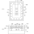
- FIG. 6(A) and FIG. 6(B) illustrate an example in a simplified manner.
- This MOS type capacitor includes a P-type semiconductor substrate 11, an N-type well 12, an N+ diffusion layer 13, an SiO 2 layer 104 for isolation, a gate insulating film 15, a gate 106 made of polycrystalline silicon or metal, and an interlayer insulating film 113. , a wiring layer 108, a protective layer 115, and a contact hole 116.
- This capacitor is formed between the gate 106 and the surface of the N-type well 12 with the gate insulating film 15 in between, like a normal MOS type capacitor.
- a parasitic capacitance may be formed between the wiring layer 108 and the N-type well 12 or the semiconductor substrate 11, or a parasitic resistance component or a parasitic inductance component may be generated in the wiring layer 108 itself.
- FIG. 7 is an equivalent circuit diagram of the MOS capacitor shown in FIGS. 6(A) and 6(B).
- the terminals T1 and T2 shown in FIG. 7 correspond to the electrodes to which the wiring layer 108 of the electronic component shown in FIGS. 6(A) and 6(B) is connected, and the capacitor C0 shown in FIG. It is a capacitor that The capacitor C1 shown in FIG. 7 is the above parasitic capacitance.
- the inductor L1 shown in FIG. 7 is the parasitic inductance component, and the resistor R1 is the parasitic resistance component.
- An object of the present invention is to provide an electronic component in which a low parasitic impedance capacitor is formed on a semiconductor substrate.
- An electronic component as an example of the present disclosure includes: a semiconductor substrate; an insulator layer formed on the surface layer side of the semiconductor substrate; an internal electrode formed within the insulator layer; a dielectric layer formed on the surface side of the semiconductor substrate; an extraction electrode that is electrically connected to the internal electrode on the surface side of the internal electrode; an external electrode that is electrically connected to the extraction electrode on the surface side of the extraction electrode; Equipped with
- the internal electrode includes a first internal electrode electrically connected to the semiconductor substrate and a second internal electrode formed on the surface side of the dielectric layer,
- the extraction electrode is configured to include a first extraction electrode electrically connected to the first internal electrode, and a second extraction electrode electrically connected to the second internal electrode,
- the external electrode is configured to include a first external electrode electrically connected to the first extraction electrode, and a second external electrode electrically connected to the second extraction electrode,
- the second extraction electrode is formed inside the second internal electrode when viewed in a direction perpendicular to the surface of the semiconductor substrate. It is characterized by
- an electronic component in which a low parasitic impedance capacitor is formed on a semiconductor substrate can be obtained.
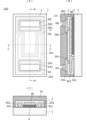
- FIG. 1(A) is a plan view of an electronic component 101 according to the first embodiment
- FIG. 1(B) is a cross-sectional view taken along the line BB in FIG. 1(A)
- FIG. is a sectional view taken along the line CC in FIG. 1(A).
- 2(A) is a plan view of the electronic component 102 according to the second embodiment
- FIG. 2(B) is a sectional view taken along the line BB in FIG. 2(A)
- FIG. is a sectional view taken along the line CC in FIG. 2(A).
- 3(A) is a plan view of the electronic component 103 according to the third embodiment
- FIG. 3(B) is a sectional view taken along the line BB in FIG. 3(A)
- 3(C) is a sectional view taken along the line BB in FIG. is a sectional view taken along the line CC in FIG. 3(A).
- 4(A) is a plan view of the electronic component 104 according to the fourth embodiment
- FIG. 4(B) is a sectional view taken along the line BB in FIG. 4(A)
- FIG. 4(C) is a sectional view taken along the line BB in FIG. is a sectional view taken along the line CC in FIG. 4(A).
- 5(A) is a plan view of the electronic component 105 according to the fifth embodiment
- FIG. 5(B) is a sectional view taken along the line BB in FIG. 5(A)
- FIGS. 6A and 6B are simplified diagrams of a MOS capacitor used in an internal voltage generation circuit of a semiconductor memory described in Patent Document 1.
- FIG. 7 is an equivalent circuit diagram of the MOS capacitor shown in FIGS. 6(A) and 6(B).
- FIG. 1(A) is a plan view of an electronic component 101 according to the first embodiment
- FIG. 1(B) is a cross-sectional view taken along the line BB in FIG. 1(A)
- FIG. is a sectional view taken along the line CC in FIG. 1(A).
- FIG. 1A is a plan view in a state before formation of a protective film 10, which will be described later.
- This electronic component 101 includes a semiconductor substrate 1, an insulator layer 2 formed on the surface side of the semiconductor substrate 1, first internal electrodes 3A1 and 3A2 formed in the insulator layer 2, and an insulator layer 2. a second internal electrode 3B formed inside, a dielectric layer 4 made of a thermal oxide film formed on the surface side of the semiconductor substrate 1, and first internal electrodes 3A1, 3A2 on the surface side from the first internal electrodes 3A1, 3A2.
- the first extraction electrodes 5A1, 5A2 are electrically connected to the second internal electrode 3B, and the second extraction electrodes 5B1, 5B2 are electrically connected to the second internal electrode 3B on the surface side of the second internal electrode 3B.
- the semiconductor substrate 1 is, for example, a substrate made of an impurity semiconductor such as a carrier-doped silicon substrate
- the insulator layer 2 is, for example, a SiN film
- the dielectric layer 4 is, for example, a thermally oxidized SiO 2 film of the semiconductor substrate 1.
- the first internal electrodes 3A1, 3A2 and the second internal electrode 3B are, for example, Al films
- the first extraction electrodes 5A1, 5A2 and the second extraction electrodes 5B1, 5B2 are, for example, Cu films.
- the first external electrode 6A and the second external electrode 6B are, for example, metal films with a Ni base and an Au surface.
- the protective film 10 is, for example, an organic insulating film such as a solder resist.
- the second internal electrode 3B constitutes a capacitor electrode formed on the dielectric layer 4. Since the semiconductor substrate 1 is a substrate made of an impurity semiconductor such as a carrier-doped silicon substrate, it has conductivity. Therefore, the semiconductor substrate 1, dielectric layer 4, and second internal electrode 3B constitute the main part of the capacitor.
- the first external electrode 6A, the first extraction electrodes 5A1, 5A2, and the first internal electrodes 3A1, 3A2 are electrically connected to the semiconductor substrate 1, and the second external electrode 6B and the second extraction electrodes 5B1, 5B2 are electrically connected to the second internal electrode 3B. do.
- the first external electrode 6A and the second external electrode 6B are used, for example, as connection pads such as wire bonding pads or surface mounting pads. Therefore, this electronic component 101 acts as a capacitor having the first external electrode 6A and the second external electrode 6B.
- the capacitor formed in the electronic component 101 of this embodiment uses a silicon semiconductor substrate as one electrode and a silicon thermal oxide film as a dielectric layer, so a highly accurate capacitance can be set.
- the second extraction electrodes 5B1, 5B2 are formed inside the second internal electrode 3B when viewed in the direction perpendicular to the surface of the semiconductor substrate 1, the second extraction electrodes 5B1, 5B2 The parasitic capacitance between the semiconductor substrate 1 and the semiconductor substrate 1 can be reduced. Further, since the second external electrode 6B that is electrically connected to the second extraction electrodes 5B1 and 5B2 is formed on the second extraction electrodes 5B1 and 5B2, parasitic inductance and parasitic resistance caused by the second extraction electrodes 5B1 and 5B2 can be suppressed.
- first extraction electrodes 5A1, 5A2 are formed on the first internal electrodes 3A1, 3A2, and a first external electrode 6A electrically connected to the first extraction electrodes 5A1, 5A2 is formed on the first extraction electrodes 5A1, 5A2. Therefore, parasitic inductance and parasitic resistance due to the first extraction electrodes 5A1 and 5A2 can also be suppressed.
- FIG. 2(A) is a plan view of the electronic component 102 according to the second embodiment
- FIG. 2(B) is a sectional view taken along the line BB in FIG. 2(A)
- FIG. is a sectional view taken along the line CC in FIG. 2(A).
- FIG. 2(A) is a plan view in a state before the protective film 10 is formed.
- This electronic component 102 includes a semiconductor substrate 1, an insulator layer 2 formed on the surface side of the semiconductor substrate 1, first internal electrodes 3A1 and 3A2 formed in the insulator layer 2, and an insulator layer 2. a second internal electrode 3B formed inside, a dielectric layer 4 made of a thermal oxide film formed on the surface side of the semiconductor substrate 1, and first internal electrodes 3A1, 3A2 on the surface side from the first internal electrodes 3A1, 3A2.
- the first extraction electrodes 5A1, 5A2 are electrically connected to the second internal electrode 3B, and the second extraction electrodes 5B1, 5B2 are electrically connected to the second internal electrode 3B on the surface side of the second internal electrode 3B.
- the semiconductor substrate 1 is, for example, a substrate made of an impurity semiconductor such as a carrier-doped silicon substrate
- the insulator layer 2 is, for example, a SiN film
- the dielectric layer 4 is, for example, a thermally oxidized SiO 2 film of the semiconductor substrate 1.
- the first internal electrodes 3A1, 3A2 and the second internal electrode 3B are, for example, Al films
- the first extraction electrodes 5A1, 5A2 and the second extraction electrodes 5B1, 5B2 are, for example, Cu films.
- the first external electrode 6A and the second external electrode 6B are, for example, metal films with a Ni base and an Au surface.
- the protective film 10 is, for example, an organic insulating film such as a solder resist.
- the shapes of the first internal electrodes 3A1, 3A2, the second internal electrode 3B, and the dielectric layer 4 are different from the electronic component 101 shown in FIGS. 1(A), 1(B), and 1(C).
- the dielectric layer 4 has a concave shape when viewed in a direction perpendicular to the surface of the semiconductor substrate 1.
- the second internal electrode 3B also has a concave shape.
- the overall shape of the first internal electrodes 3A1, 3A2 is convex, and the facing portions of the first internal electrodes 3A1, 3A2 and the second internal electrode 3B face each other in an uneven manner.
- the first internal electrode 3A1 has a linear portion extending toward the second external electrode 6B, and the second internal electrode 3B is arranged so as to surround the extended portion. Furthermore, as can be seen from FIG. 2A, the distance between the sides of the first internal electrode 3A1 and the second internal electrode 3B is constant in the area where the first internal electrode 3A1 and the second internal electrode 3B face each other. The first internal electrode 3A1 and the second internal electrode 3B are formed such that the distance between the two sides is constant.
- the second internal electrode 3B constitutes a capacitor electrode formed on the dielectric layer 4.
- the semiconductor substrate 1, dielectric layer 4, and second internal electrode 3B constitute the main part of the capacitor.
- the other configurations are similar to the electronic component 101 shown in the first embodiment.
- the average path length of the current flowing laterally through the semiconductor substrate 1 is shortened.
- the area of the conductive portion between the first internal electrode 3A1 and the semiconductor substrate 1 can be made smaller, so a capacitor with higher capacitance density can be formed.
- the third embodiment exemplifies an electronic component in which the configurations of internal electrodes and dielectric layers are different from those shown in the first and second embodiments.
- FIG. 3(A) is a plan view of the electronic component 103 according to the third embodiment
- FIG. 3(B) is a sectional view taken along the line BB in FIG. 3(A)
- FIG. 3(C) is a sectional view taken along the line BB in FIG. is a sectional view taken along the line CC in FIG. 3(A).
- FIG. 3(A) is a plan view in a state before the protective film 10 is formed.
- This electronic component 103 includes a semiconductor substrate 1, an insulator layer 2 formed on the surface side of the semiconductor substrate 1, first internal electrodes 3A1 and 3A2 formed in the insulator layer 2, and an insulator layer 2. a second internal electrode 3B formed inside, a dielectric layer 4 made of a thermal oxide film formed on the surface side of the semiconductor substrate 1, and first internal electrodes 3A1, 3A2 on the surface side from the first internal electrodes 3A1, 3A2.
- the first extraction electrodes 5A1, 5A2 are electrically connected to the second internal electrode 3B, and the second extraction electrodes 5B1, 5B2 are electrically connected to the second internal electrode 3B on the surface side of the second internal electrode 3B.
- the shapes of the first internal electrodes 3A1, 3A2 and the dielectric layer 4 are different from the electronic component 102 shown in FIGS. 2(A), 2(B), and 2(C).
- the dielectric layer 4 is also formed on the lower surface of the first internal electrode 3A2 when viewed in the direction perpendicular to the surface of the semiconductor substrate 1. Further, the first internal electrode 3A1 is formed within the opening of the dielectric layer 4.
- the second internal electrode 3B constitutes a capacitor electrode formed on the dielectric layer 4.
- the semiconductor substrate 1, dielectric layer 4, and second internal electrode 3B constitute the main part of the capacitor.
- the other configurations are similar to the electronic component 102 shown in the second embodiment.
- the dielectric layer 4 below the first internal electrode 3A2 acts as a height adjustment layer for the first internal electrode 3A2. That is, in the step of forming the first internal electrode 3A2, the first internal electrode 3A2 is prevented from sagging toward the semiconductor substrate 1 side. As a result, the heights of the first external electrode 6A and the second external electrode 6B tend to be the same. As a result, the accuracy of wire bonding to the first external electrode 6A and the second external electrode 6B when wire bonding the electronic component 103 can be improved. Alternatively, it is possible to prevent impact from being concentrated on one external electrode when the electronic component 103 is surface mounted.
- the portion that constitutes the height adjustment layer of the first internal electrode 3A2 for making the heights of the first external electrode 6A and the second external electrode 6B equal, and the portion that constitutes the main part of the capacitor are made of dielectric material. They may be formed so that the layer 4 is a separate body.
- FIG. 4(A) is a plan view of the electronic component 104 according to the fourth embodiment
- FIG. 4(B) is a sectional view taken along the line BB in FIG. 4(A)
- FIG. 4(C) is a sectional view taken along the line BB in FIG. is a sectional view taken along the line CC in FIG. 4(A).
- FIG. 4A is a plan view in a state before the protective film 10 is formed.
- the dielectric layer 4 and the second internal electrode 3B are formed in a planar shape on the top of the semiconductor substrate 1, but in the electronic component 104 of the fourth embodiment, A plurality of trenches are formed in the upper part of the semiconductor substrate 1.
- the trench in this example is not groove-like but cylindrical.
- a dielectric layer 4 is formed on the inner surface of these trenches, and a portion of the second internal electrode 3B is buried therein.
- the opposing area between the second internal electrode 3B and the semiconductor substrate 1 via the dielectric layer 4 can be increased, so the planar area of the capacitor formation region can be saved.
- the fifth embodiment exemplifies an electronic component in which the configurations of internal electrodes and dielectric layers are different from those shown in the first and second embodiments.
- FIG. 5(A) is a plan view of the electronic component 105 according to the fifth embodiment
- FIG. 5(B) is a sectional view taken along the line BB in FIG. 5(A)
- FIG. 5(C) is a sectional view taken along the line BB in FIG. is a cross-sectional view taken along the line CC in FIG. 5(A).
- FIG. 5A is a plan view in a state before the protective film 10 is formed.
- This electronic component 105 includes a semiconductor substrate 1, an insulator layer 2 formed on the surface side of the semiconductor substrate 1, first internal electrodes 3A1 and 3A2 formed in the insulator layer 2, and an insulator layer 2. a second internal electrode 3B formed inside, a dielectric layer 4 made of a thermal oxide film formed on the surface side of the semiconductor substrate 1, and first internal electrodes 3A1, 3A2 on the surface side from the first internal electrodes 3A1, 3A2.
- the first extraction electrodes 5A1, 5A2 are electrically connected to the second internal electrode 3B, and the second extraction electrodes 5B1, 5B2 are electrically connected to the second internal electrode 3B on the surface side of the second internal electrode 3B.
- the dielectric layer 4 and the second internal electrode 3B have a concave shape when viewed in the direction perpendicular to the surface of the semiconductor substrate 1.
- the overall shape of the first internal electrodes 3A1 and 3A2 was convex, but in the electronic component 105 according to the fifth embodiment, the dielectric layer 4 and the second internal electrode 3B are convex, and the first internal electrode 3A1 and 3A2 have a convex shape.
- the overall shape of the electrodes 3A1 and 3A2 is concave.
- the facing portions of the first internal electrodes 3A1 and 3A2 and the second internal electrode 3B face each other in an uneven manner.
- the second internal electrode 3B extends linearly toward the first external electrode 6A, and the second internal electrode 3B is arranged so that the first internal electrode 3A1 surrounds the extended part of the second internal electrode 3B. has been done. Further, in the region where the first internal electrode 3A1 and the second internal electrode 3B face each other, the distance between the sides is constant (the distance between the facing sides of the first internal electrode 3A1 and the second internal electrode 3B is constant). The first internal electrode 3A1 and the second internal electrode 3B are formed in this manner.
- an electronic component including a capacitor and an inductor is shown as a passive component, but the present invention can be similarly applied to an electronic component including an active component as well as a passive component.
- the opposing portions of the second internal electrode 3B and the first internal electrodes 3A1 and 3A2 when viewed in a direction perpendicular to the surface of the semiconductor substrate 1, are electronic components that face each other in an uneven manner.
Landscapes
- Engineering & Computer Science (AREA)
- Power Engineering (AREA)
- Microelectronics & Electronic Packaging (AREA)
- Manufacturing & Machinery (AREA)
- Semiconductor Integrated Circuits (AREA)
Priority Applications (3)
| Application Number | Priority Date | Filing Date | Title |
|---|---|---|---|
| CN202380029119.9A CN118974862A (zh) | 2022-03-23 | 2023-03-13 | 电子部件 |
| JP2024510032A JP7798176B2 (ja) | 2022-03-23 | 2023-03-13 | 電子部品 |
| US18/887,578 US20250014833A1 (en) | 2022-03-23 | 2024-09-17 | Electronic component |
Applications Claiming Priority (2)
| Application Number | Priority Date | Filing Date | Title |
|---|---|---|---|
| JP2022047045 | 2022-03-23 | ||
| JP2022-047045 | 2022-03-23 |
Related Child Applications (1)
| Application Number | Title | Priority Date | Filing Date |
|---|---|---|---|
| US18/887,578 Continuation US20250014833A1 (en) | 2022-03-23 | 2024-09-17 | Electronic component |
Publications (1)
| Publication Number | Publication Date |
|---|---|
| WO2023182051A1 true WO2023182051A1 (ja) | 2023-09-28 |
Family
ID=88101360
Family Applications (1)
| Application Number | Title | Priority Date | Filing Date |
|---|---|---|---|
| PCT/JP2023/009641 Ceased WO2023182051A1 (ja) | 2022-03-23 | 2023-03-13 | 電子部品 |
Country Status (4)
| Country | Link |
|---|---|
| US (1) | US20250014833A1 (https=) |
| JP (1) | JP7798176B2 (https=) |
| CN (1) | CN118974862A (https=) |
| WO (1) | WO2023182051A1 (https=) |
Citations (3)
| Publication number | Priority date | Publication date | Assignee | Title |
|---|---|---|---|---|
| JPH0547586A (ja) * | 1991-08-16 | 1993-02-26 | Toshiba Corp | コンデンサ部品 |
| JP2017208528A (ja) * | 2016-05-19 | 2017-11-24 | サムソン エレクトロ−メカニックス カンパニーリミテッド. | 薄膜キャパシター及びその製造方法 |
| JP2021057374A (ja) * | 2019-09-27 | 2021-04-08 | 太陽誘電株式会社 | キャパシタ |
-
2023
- 2023-03-13 CN CN202380029119.9A patent/CN118974862A/zh active Pending
- 2023-03-13 JP JP2024510032A patent/JP7798176B2/ja active Active
- 2023-03-13 WO PCT/JP2023/009641 patent/WO2023182051A1/ja not_active Ceased
-
2024
- 2024-09-17 US US18/887,578 patent/US20250014833A1/en active Pending
Patent Citations (3)
| Publication number | Priority date | Publication date | Assignee | Title |
|---|---|---|---|---|
| JPH0547586A (ja) * | 1991-08-16 | 1993-02-26 | Toshiba Corp | コンデンサ部品 |
| JP2017208528A (ja) * | 2016-05-19 | 2017-11-24 | サムソン エレクトロ−メカニックス カンパニーリミテッド. | 薄膜キャパシター及びその製造方法 |
| JP2021057374A (ja) * | 2019-09-27 | 2021-04-08 | 太陽誘電株式会社 | キャパシタ |
Also Published As
| Publication number | Publication date |
|---|---|
| JP7798176B2 (ja) | 2026-01-14 |
| JPWO2023182051A1 (https=) | 2023-09-28 |
| CN118974862A (zh) | 2024-11-15 |
| US20250014833A1 (en) | 2025-01-09 |
Similar Documents
| Publication | Publication Date | Title |
|---|---|---|
| US8076755B2 (en) | Semiconductor device and method of manufacturing the same | |
| TWI472031B (zh) | 半導體裝置 | |
| US20190348496A1 (en) | Capacitor | |
| US8187930B2 (en) | Structure and layout of a FET prime cell | |
| JP2005142531A (ja) | Mim構造抵抗体を搭載した半導体装置 | |
| KR100398164B1 (ko) | 절연게이트반도체장치 | |
| JP5601072B2 (ja) | 半導体装置 | |
| US20050093668A1 (en) | Coil on a semiconductor substrate and method for its production | |
| JP2001118988A (ja) | 半導体装置 | |
| US7560774B1 (en) | IC chip | |
| JP6923303B2 (ja) | ダイオード素子 | |
| WO2023182051A1 (ja) | 電子部品 | |
| JP2006229226A (ja) | 集積回路を有する半導体装置 | |
| US20040238871A1 (en) | Semiconductor device | |
| US20210273118A1 (en) | Semiconductor Device | |
| JP7180842B2 (ja) | 半導体装置 | |
| CN214336713U (zh) | 一种半导体器件 | |
| CN112310229A (zh) | 电容结构 | |
| KR100471520B1 (ko) | 반도체디바이스 | |
| JP5401056B2 (ja) | 半導体装置 | |
| KR100448085B1 (ko) | 패드의기생캐패시턴스감소형반도체장치 | |
| TWI485836B (zh) | 化合物半導體裝置及其製造方法 | |
| JP2022181358A (ja) | 半導体装置 | |
| WO2023181803A1 (ja) | 電子部品及び回路装置 | |
| CN113410200A (zh) | 一种芯片封装框架和芯片封装结构 |
Legal Events
| Date | Code | Title | Description |
|---|---|---|---|
| 121 | Ep: the epo has been informed by wipo that ep was designated in this application |
Ref document number: 23774648 Country of ref document: EP Kind code of ref document: A1 |
|
| ENP | Entry into the national phase |
Ref document number: 2024510032 Country of ref document: JP Kind code of ref document: A |
|
| WWE | Wipo information: entry into national phase |
Ref document number: 202380029119.9 Country of ref document: CN |
|
| NENP | Non-entry into the national phase |
Ref country code: DE |
|
| 122 | Ep: pct application non-entry in european phase |
Ref document number: 23774648 Country of ref document: EP Kind code of ref document: A1 |