WO2023176351A1 - 半導体発光装置および半導体発光装置の実装構造体 - Google Patents
半導体発光装置および半導体発光装置の実装構造体 Download PDFInfo
- Publication number
- WO2023176351A1 WO2023176351A1 PCT/JP2023/006514 JP2023006514W WO2023176351A1 WO 2023176351 A1 WO2023176351 A1 WO 2023176351A1 JP 2023006514 W JP2023006514 W JP 2023006514W WO 2023176351 A1 WO2023176351 A1 WO 2023176351A1
- Authority
- WO
- WIPO (PCT)
- Prior art keywords
- mounting
- semiconductor light
- light emitting
- emitting device
- section
- Prior art date
- Legal status (The legal status is an assumption and is not a legal conclusion. Google has not performed a legal analysis and makes no representation as to the accuracy of the status listed.)
- Ceased
Links
Images


Classifications
-
- H—ELECTRICITY
- H10—SEMICONDUCTOR DEVICES; ELECTRIC SOLID-STATE DEVICES NOT OTHERWISE PROVIDED FOR
- H10H—INORGANIC LIGHT-EMITTING SEMICONDUCTOR DEVICES HAVING POTENTIAL BARRIERS
- H10H20/00—Individual inorganic light-emitting semiconductor devices having potential barriers, e.g. light-emitting diodes [LED]
- H10H20/80—Constructional details
- H10H20/85—Packages
- H10H20/857—Interconnections, e.g. lead-frames, bond wires or solder balls
Definitions
- the present disclosure relates to a semiconductor light emitting device and a mounting structure for the semiconductor light emitting device.
- Patent Document 1 discloses an example of a conventional semiconductor light emitting device.
- the semiconductor light emitting device disclosed in the document includes a substrate, a semiconductor light emitting device, and a sealing resin.
- the semiconductor light emitting device is mounted on the main surface of the substrate.
- the sealing resin covers the semiconductor light emitting element and transmits light from the semiconductor light emitting element.
- This semiconductor device is mounted on a mounting board with its bottom surface facing the mounting board.
- the semiconductor light emitting device be mounted on a mounting board with high mounting strength. Further, when mounting the semiconductor light emitting device, it is preferable to make the semiconductor light emitting device more stable on the mounting substrate.
- An object of the present disclosure is to provide a semiconductor light-emitting device (and by extension, a mounting structure for the semiconductor light-emitting device) that is improved over conventional ones.
- one object of the present disclosure is to provide a semiconductor light-emitting device that has improved mounting strength and can be mounted more stably, and to provide a mounting structure for the semiconductor light-emitting device. Take it as a challenge.
- a semiconductor light emitting device provided by the first aspect of the present disclosure includes a substrate having a base material and a wiring section, and a semiconductor light emitting element.
- the base material has a first surface and a second surface facing opposite to each other in the thickness direction, and a surface located between the first surface and the second surface in the thickness direction and perpendicular to the thickness direction. and a third surface facing one side in the first direction.
- the semiconductor light emitting device is supported by the first surface.
- the wiring section includes a first mounting section disposed on the first surface and used for mounting, a second mounting section disposed on the second surface and used for mounting, and exposed from the third surface. and a third mounting section for use in mounting.
- a mounting structure for a semiconductor light emitting device provided by a second aspect of the present disclosure includes the semiconductor light emitting device provided by the first aspect of the present disclosure, and a mounting substrate on which the semiconductor light emitting device is mounted. .
- the thickness direction is included in the in-plane direction of the mounting board.
- a third joint portion that conducts conductive joint is provided.
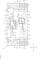
- FIG. 1 is a perspective view showing a semiconductor light emitting device and a mounting structure for the semiconductor light emitting device according to a first embodiment of the present disclosure.
- FIG. 2 is a plan view showing a semiconductor light emitting device according to the first embodiment of the present disclosure.
- FIG. 3 is a front view showing the semiconductor light emitting device according to the first embodiment of the present disclosure.
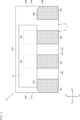
- FIG. 4 is a bottom view showing the semiconductor light emitting device according to the first embodiment of the present disclosure.
- FIG. 5 is a right side view showing the semiconductor light emitting device according to the first embodiment of the present disclosure.
- FIG. 6 is a left side view showing the semiconductor light emitting device according to the first embodiment of the present disclosure.
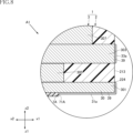
- FIG. 7 is a cross-sectional view taken along line VII-VII in FIG. FIG.
- FIG. 8 is an enlarged sectional view of a main part of a semiconductor light emitting device according to a first embodiment of the present disclosure.
- FIG. 9 is an enlarged sectional view of a main part of a semiconductor light emitting device according to a first embodiment of the present disclosure.
- FIG. 10 is a plan view of main parts showing a semiconductor light emitting device according to the first embodiment of the present disclosure.
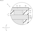
- FIG. 11 is a sectional view taken along line XI-XI in FIG.
- FIG. 12 is an enlarged cross-sectional view of essential parts showing a semiconductor light emitting device according to the first embodiment of the present disclosure.
- FIG. 13 is a cross-sectional view taken along line XIII-XIII in FIG. FIG.
- FIG. 14 is an enlarged sectional view of a main part of a semiconductor light emitting device according to a first embodiment of the present disclosure.
- FIG. 15 is a rear view showing a semiconductor light emitting device and a mounting structure for the semiconductor light emitting device according to the first embodiment of the present disclosure.
- FIG. 16 is a rear view showing a first modification of the mounting structure for a semiconductor light emitting device according to the first embodiment of the present disclosure.
- FIG. 17 is a bottom view showing a semiconductor light emitting device according to a second embodiment of the present disclosure.
- FIG. 18 is a rear view showing a semiconductor light emitting device and a mounting structure for the semiconductor light emitting device according to the second embodiment of the present disclosure.
- FIG. 15 is a rear view showing a semiconductor light emitting device and a mounting structure for the semiconductor light emitting device according to the first embodiment of the present disclosure.
- FIG. 16 is a rear view showing a first modification of the mounting structure for a semiconductor light emitting device according to the first embodiment of the
- FIG. 19 is a plan view showing a semiconductor light emitting device according to a third embodiment of the present disclosure.
- FIG. 20 is a bottom view showing a semiconductor light emitting device according to a third embodiment of the present disclosure.
- FIG. 21 is a right side view showing a semiconductor light emitting device according to a third embodiment of the present disclosure.
- a thing A is formed on a thing B and "a thing A is formed on a thing B” mean “a thing A is formed on a thing B” unless otherwise specified.
- "something A is placed on something B” and “something A is placed on something B” mean "something A is placed on something B” unless otherwise specified.
- the semiconductor light emitting device A1 of this embodiment includes a substrate 1, semiconductor light emitting elements 4A, 4B, wires 51, 52, 53, a sealing resin 6, and insulating layers 7A, 7B.
- FIG. 1 is a perspective view showing a semiconductor light emitting device A1 and a mounting structure B1.
- FIG. 2 is a plan view showing the semiconductor light emitting device A1.
- FIG. 3 is a front view showing the semiconductor light emitting device A1.
- FIG. 4 is a bottom view showing the semiconductor light emitting device A1.
- FIG. 5 is a right side view showing the semiconductor light emitting device A1.
- FIG. 6 is a left side view showing the semiconductor light emitting device A1.
- FIG. 7 is a cross-sectional view taken along line VII-VII in FIG.
- FIG. 8 is an enlarged sectional view of the main parts of the semiconductor light emitting device A1.
- FIG. 9 is an enlarged cross-sectional view of the main parts of the semiconductor light emitting device A1.
- FIG. 1 is a perspective view showing a semiconductor light emitting device A1 and a mounting structure B1.
- FIG. 2 is a plan view showing the semiconductor light emitting device A1.
- FIG. 3 is a front view showing
- FIG. 10 is a plan view of essential parts of the semiconductor light emitting device A1.
- FIG. 11 is a sectional view taken along line XI-XI in FIG.
- FIG. 12 is an enlarged cross-sectional view of the main parts of the semiconductor light emitting device A1.
- FIG. 13 is a cross-sectional view taken along line XIII-XIII in FIG.
- FIG. 14 is an enlarged cross-sectional view of the main parts of the semiconductor light emitting device A1.
- FIG. 15 is a rear view showing the semiconductor light emitting device A1 and the mounting structure B1.
- the z direction is an example of the thickness direction of the present disclosure
- the x direction is an example of the first direction of the present disclosure
- the y direction is an example of the second direction of the present disclosure.
- the substrate 1 supports the semiconductor light emitting devices 4A and 4B, and also forms a conductive path for supplying power to cause the semiconductor light emitting devices 4A and 4B to emit light.
- the substrate 1 has a base material 2 and a wiring section 3.
- the base material 2 includes an insulating material such as glass epoxy resin.
- the size of the base material 2 is not limited at all, and for example, the size in the x direction is about 1.6 mm, the size in the y direction is about 0.8 mm, and the size in the z direction is about 0.6 mm.
- the base material 2 may have a structure in which the whole is formed integrally, or may have a structure in which a plurality of layers are laminated.
- the base material 2 may include a first base layer 201, a second base layer 202, and a third base layer 203.
- the first base layer 201 is located on the z1 side in the z direction and forms a first surface 211.
- the second base material layer 202 is located on the z2 side in the z direction, and forms a second surface 212.
- the third base layer 203 is located between the first base layer 201 and the second base layer 202 in the z direction.
- the base material 2 has a first surface 211, a second surface 212, a third surface 213, a fourth surface 214, a fifth surface 215, and a sixth surface 216.
- the first surface 211 is a plane facing the z1 side in the z direction.
- the second surface 212 is a plane facing the z2 side in the z direction.
- the third surface 213 is located between the first surface 211 and the second surface 212 in the z direction, and faces the x1 side in the x direction.
- the fourth surface 214 is located between the first surface 211 and the second surface 212 in the z direction, and faces the x2 side in the x direction.
- the fifth surface 215 is located between the first surface 211 and the second surface 212 in the z direction, and faces the y1 side in the y direction.
- the sixth surface 216 is located between the first surface 211 and the second surface 212 in the z direction, and faces the y2 side in the y direction.
- the first surface 211 has a first edge 221, a fourth edge 224, and a seventh edge 227.
- the first edge 221 is the edge of the first surface 211 on the y1 side in the y direction, and extends in the x direction.
- the fourth edge 224 is an edge of the first surface 211 on the x1 side in the x direction, and extends in the y direction.
- the seventh edge 227 is an edge of the first surface 211 on the x2 side in the x direction, and extends in the y direction.
- the second surface 212 has a second edge 222, a fifth edge 225, and an eighth edge 228.
- the second edge 222 is the edge of the second surface 212 on the y1 side in the y direction, and extends in the x direction.
- the fifth edge 225 is an edge of the second surface 212 on the x1 side in the x direction, and extends in the y direction.
- the eighth edge 228 is an edge of the second surface 212 on the x2 side in the x direction, and extends in the y direction.
- the third surface 213 has a third edge 223.
- the third edge 223 is the edge of the third surface 213 on the y1 side in the y direction, and extends in the z direction.
- the fourth edge 224 also serves as a boundary between the first surface 211 and the third surface 213.
- the fifth edge 225 also serves as a boundary between the second surface 212 and the third surface 213.
- the third edge 223 also serves as a boundary between the third surface 213 and the fifth surface 215.
- the fourth surface 214 has a sixth edge 226.
- the sixth edge 226 is the edge of the fourth surface 214 on the y1 side in the y direction, and extends in the z direction.
- the seventh edge 227 also serves as a boundary between the first surface 211 and the fourth surface 214.
- the eighth edge 228 also serves as a boundary between the second surface 212 and the fourth surface 214.
- the sixth edge 226 also serves as a boundary between the fourth surface 214 and the fifth surface 215.
- the wiring section 3 is arranged on or inside the base material 2.
- the wiring part 3 is made of a conductive material such as metals such as Cu (copper), Ni (nickel), Fe (iron), Sn (tin), Ag (silver), Au (gold), or alloys thereof. include.
- the method of forming the wiring portion 3 is not limited at all, and may be formed by plating, for example.
- the wiring section 3 of this embodiment has a base 30 and a metal layer 39.
- the base portion 30 is a portion that becomes the main body of the wiring portion 3, and includes metals such as Cu (copper), Ni (nickel), and Fe (iron), or alloys thereof.
- the metal layer 39 is laminated on a portion of the base 30 exposed from the sealing resin 6 and the insulating layers 7A and 7B.
- the metal layer 39 contains, for example, Sn (tin).
- the metal layer 39 is formed, for example, by a technique such as barrel plating after mounting the semiconductor light emitting elements 4A, 4B and forming the sealing resin 6 and the insulating layers 7A, 7B. In FIGS. 1 to 6 and FIG.
- the region where the metal layer 39 is formed is hatched with a plurality of discrete points. Note that the method of forming the metal layer 39 and the region in which it is formed are not limited at all. Further, if the base portion 30 has sufficient wettability with respect to molten solder, for example, the wiring portion 3 may be configured without the metal layer 39.
- the wiring section 3 of this embodiment includes a first layer 301, a second layer 302, a third layer 303, a fourth layer 304, a plurality of through conductive parts 305, a plurality of through conductive parts 305, and a plurality of through conductive parts 305. portion 306 and a plurality of through conductive portions 307.
- the first layer 301 is arranged on the first surface 211 (first base layer 201) of the base material 2.
- the specific configuration of the first layer 301 is not limited at all, and in this embodiment, as shown in FIGS. It has a bonding part 321, a wire bonding part 322, a wire bonding part 323, a pad part 331, a pad part 332, a pad part 333, a pad part 334, a connecting part 341, and a connecting part 342.
- the die bonding part 311 is a part to which the semiconductor light emitting element 4A is die bonded.
- the die bonding portion 311 is spaced apart from the first edge 221 , the fourth edge 224 , the seventh edge 227 , and the sixth surface 216 .
- the die bonding portion 312 is a portion to which the semiconductor light emitting device 4B is die bonded.
- the die bonding part 312 is located on the y2 side in the y direction with respect to the die bonding part 311, and is spaced apart from the first edge 221, the fourth edge 224, the seventh edge 227, and the sixth surface 216. ing.
- die bonding section 311 and die bonding section 312 are connected to each other.
- the wire bonding part 321 is a part to which the wire 51 is bonded.
- the wire bonding section 321 is spaced apart from the die bonding section 311 on the x2 side in the x direction.
- the wire bonding portion 322 is a portion to which the wire 52 is bonded.
- the wire bonding section 322 is spaced apart from the die bonding section 312 on the x1 side in the x direction.
- the wire bonding portion 323 is a portion to which the wire 53 is bonded.
- the wire bonding section 323 is spaced apart from the die bonding section 312 on the x2 side in the x direction. Furthermore, the wire bonding section 323 is spaced apart from the wire bonding section 321 on the y2 side in the y direction.
- the pad section 331 is located on the x1 side in the x direction with respect to the die bonding section 311.
- the pad portion 331 is in contact with the first edge 221. Further, the pad portion 331 is in contact with the fourth end edge 224.
- the connecting portion 341 connects the die bonding portion 311 and the pad portion 331.
- the connecting portion 341 has a band shape extending in the x direction.
- the pad portion 332 is located on the x2 side in the x direction with respect to the wire bonding portion 321.
- the pad portion 332 is in contact with the first edge 221. Further, the pad portion 332 is in contact with the seventh end edge 227.
- the connecting portion 342 connects the wire bonding portion 321 and the wire bonding portion 323.
- the connecting portion 342 has a band shape extending in the x direction.
- the pad portion 333 is located on the x1 side in the x direction with respect to the wire bonding portion 322.
- the pad portion 333 is in contact with the fourth edge 224. Further, the pad portion 333 is in contact with the sixth surface 216.
- the pad portion 333 and the wire bonding portion 322 are connected to each other.
- the pad portion 334 is located on the x2 side in the x direction with respect to the wire bonding portion 323.
- the pad portion 334 is in contact with the seventh edge 227. Further, the pad portion 334 is in contact with the sixth surface 216.
- the pad section 334 and the wire bonding section 323 are connected to each other.
- the insulating layers 7A and 7B cover a part of the first layer 301 and a part of the first surface 211.
- the specific structure of the insulating layers 7A and 7B is not limited at all, and is formed of, for example, a resist layer.
- the insulating layer 7A covers a portion of the pad portion 331 and a portion of the pad portion 333.
- the insulating layer 7A is in contact with the first edge 221, the fourth edge 224, and the sixth surface 216.
- the insulating layer 7A has a recess 71A and a recess 72A.
- the recessed portion 71A is recessed from the first edge 221 toward the y2 side in the y direction, and is recessed from the fourth edge 224 toward the x2 side in the x direction.
- the shape of the recessed portion 71A is not limited at all, and in the illustrated example, it is rectangular.
- the portion of the pad portion 331 exposed from the recessed portion 71A is the first mounting portion 31a.
- the first mounting portion 31a has a structure in which the base portion 30 is covered with a metal layer 39.
- the first mounting portion 31a is in contact with the first edge 221.
- the first mounting portion 31a is in contact with the fourth edge 224.
- the first mounting portion 31a is partitioned by an insulating layer 7A.
- the insulating layer 7A is in contact with the first mounting portion 31a.
- the recessed portion 72A is located on the y2 side in the y direction with respect to the recessed portion 71A, and is recessed on the x1 side in the x direction.
- the recessed portion 72A overlaps the pad portion 333 and has, for example, an arc shape.
- the insulating layer 7B covers a portion of the pad portion 332 and a portion of the pad portion 334.
- the insulating layer 7B is in contact with the first edge 221, the seventh edge 227, and the sixth surface 216.
- the insulating layer 7B has a recess 71B and a recess 72B.
- the recessed portion 71B is recessed from the first end edge 221 toward the y2 side in the y direction, and is recessed from the seventh end edge 227 toward the x1 side in the x direction.
- the shape of the recess 71B is not limited at all, and in the illustrated example, it is rectangular.
- the portion of the pad portion 332 exposed from the recess 71B is the first mounting portion 31b.
- the first mounting section 31b has a structure in which the base 30 is covered with a metal layer 39, similar to the first mounting section 31a.
- the first mounting portion 31b is in contact with the first edge 221.
- the first mounting portion 31b is in contact with the seventh edge 227.
- the first mounting portion 31b is partitioned by an insulating layer 7B.
- the insulating layer 7B is in contact with the first mounting portion 31b.
- the recess 72B is located on the y2 side in the y direction with respect to the recess 71B, and is recessed on the x2 side in the x direction.
- the recessed portion 72B overlaps the pad portion 334 and has, for example, an arc shape.
- the second layer 302 is arranged on the second surface 212 (second base material layer 202) of the base material 2.
- the specific configuration of the second layer 302 is not limited at all, and in this embodiment, the second layer 302 includes pad portions 335, 336, 337, and 338, as shown in FIG.
- the pad portions 335, 336, 337, and 338 are lined up in the x direction.
- the pad portions 335, 336, 337, and 338 are in contact with the second edge 222.
- the pad portion 335 is in contact with the third surface 213.
- the pad portion 336 is in contact with the eighth edge 228.
- Pad section 337 is located between pad section 335 and pad section 336 in the x direction.
- Pad section 338 is located between pad section 337 and pad section 336 in the x direction.
- the pad section 335 is the second mounting section 32a
- the pad section 336 is the second mounting section 32b.
- the second mounting portion 32a has a base portion 30 covered with a metal layer 39, and the same applies to the second mounting portion 32b, the second mounting portion 32c, and the second mounting portion 32d.
- a portion of each of the pad portion 337 and the pad portion 338 is covered with an insulating layer 7X.
- a portion of the pad portion 337 exposed from the insulating layer 7X is the second mounting portion 32c.
- a portion of the pad portion 338 exposed from the insulating layer 7X is a second mounting portion 32d.
- the specific structure of the insulating layer 7X is not limited at all, and is formed of a resist layer, for example.
- the first mounting section 31a and the second mounting section 32a overlap when viewed in the z direction. Furthermore, when viewed in the z direction, the first mounting section 31b and the second mounting section 32b overlap.
- the second mounting section 32c does not overlap the first mounting section 31a and the first mounting section 31b when viewed in the z direction. Furthermore, the second mounting section 32d does not overlap the first mounting section 31a and the first mounting section 31b when viewed in the z direction.
- the third layer 303 is located between the first layer 301 and the second layer 302 when viewed in the z direction, and has both sides in the z direction facing the base material 2. covered by.
- the third layer 303 is sandwiched between the first base layer 201 and the third base layer 203.
- the third layer 303 of this embodiment has pad portions 351a, 352a, 351b, 352b and strip portions 353a, 353b.
- the end surface of the pad portion 351a is exposed from the third surface 213 and the fifth surface 215, and is spaced apart from the sixth surface 216.
- the pad portion 351a overlaps the pad portion 331 when viewed in the z direction.
- the pad portion 351a includes a partially circular shape.
- the end surface of the pad portion 351a exposed from the third surface 213 constitutes the third mounting portion 33a.
- the third mounting portion 33a has a configuration in which a metal layer 39 is provided on the end surface of the base portion 30.
- an end surface 35a of the pad portion 351a exposed from the fifth surface 215 is covered with a metal layer 39.
- the end face of the pad portion 351b is exposed from the fourth surface 214 and the fifth surface 215, and is spaced apart from the sixth surface 216.
- the pad portion 351b overlaps the pad portion 332 when viewed in the z direction.
- the pad portion 351b includes a partially circular shape.
- the end surface of the pad portion 351b exposed from the fourth surface 214 constitutes the third mounting portion 33b.
- the configuration of the third mounting section 33b is similar to the third mounting section 33a described with reference to FIG. 12. Further, an end surface 35b of the pad portion 351b exposed from the fifth surface 215 is covered with a metal layer 39.
- the end face of the pad portion 352a is exposed from the third surface 213 and the sixth surface 216, and is spaced apart from the fifth surface 215.
- the pad portion 352a overlaps the pad portion 333 when viewed in the z direction.
- the pad portion 352a includes a partially circular shape. End surfaces of the pad portion 352a exposed from the third surface 213 and the sixth surface 216 are covered with a metal layer 39.
- the end surface of the pad portion 352b is exposed from the fourth surface 214 and the sixth surface 216, and is spaced apart from the fifth surface 215.
- the pad portion 352b overlaps the pad portion 334 when viewed in the z direction.
- pad portion 352b includes a partially circular shape.
- the end faces of the pad portion 352b exposed from the fourth surface 214 and the sixth surface 216 are covered with the metal layer 39.
- the strip portion 353a is connected to the pad portion 352a.
- the strip portion 353a includes a portion extending from the pad portion 352a toward the x2 side in the x direction, and a portion extending from the portion toward the y1 side in the y direction between the pad portion 351a and the pad portion 351b.
- the end surface 35c of the band-shaped portion 353a is exposed from the fifth surface 215 and covered with the metal layer 39.
- the strip portion 353b is connected to the pad portion 352b.
- the strip portion 353b includes a portion extending from the pad portion 352b toward the x1 side in the x direction, and a portion extending from the portion toward the y1 side in the y direction between the pad portions 351a and 351b.
- An end surface 35d of the strip portion 353b is exposed from the fifth surface 215 and is covered with the metal layer 39.
- the fourth layer 304 is located between the third layer 303 and the second layer 302 when viewed in the z direction, and has both sides in the z direction facing the base material 2. covered by.
- the fourth layer 304 is sandwiched between the third base layer 203 and the second base layer 202.
- the fourth layer 304 of this embodiment has pad portions 361a, 362a, 363a, 361b, 362b, 363b and strip portions 364a, 364b, 365a, 365b, 366b.
- the end face of the pad portion 361a is exposed from the third surface 213 and the fifth surface 215, and is spaced apart from the sixth surface 216.
- Pad portion 361a overlaps pad portion 351a and pad portion 335 when viewed in the z direction.
- the pad portion 361a includes a partially circular shape.
- the end surface of the pad portion 361a exposed from the third surface 213 constitutes the fourth mounting portion 34a.
- the fourth mounting portion 34a has a configuration in which a metal layer 39 is provided on the end surface of the base portion 30. Further, an end surface 36a of the pad portion 361a exposed from the fifth surface 215 is covered with a metal layer 39.
- the end face of the pad portion 361b is exposed from the fourth surface 214 and the fifth surface 215, and is spaced apart from the sixth surface 216.
- Pad portion 361b overlaps pad portion 351b and pad portion 336 when viewed in the z direction.
- the pad portion 361b includes a partially circular shape.
- the end surface of the pad portion 361b exposed from the fourth surface 214 constitutes the fourth mounting portion 34b.
- the configuration of the fourth mounting section 34b is similar to the third mounting section 33a described with reference to FIG. 14. Further, an end surface 36b of the pad portion 361b exposed from the fifth surface 215 is covered with a metal layer 39.
- the pad portion 362a is located between the pad portion 361a and the pad portion 361b in the x direction, and is located on the y2 side with respect to the pad portion 361a and the pad portion 361b in the y direction.
- the pad portion 362a is spaced apart from the third surface 213, fourth surface 214, fifth surface 215, and sixth surface 216.
- the pad portion 362a overlaps the pad portion 337 when viewed in the z direction.
- the pad portion 362a has a circular shape.
- the pad section 362b is located between the pad section 362z and the pad section 361b in the x direction, and between the pad section 362z and the pad section 361b in the y direction.
- the pad portion 362b is spaced apart from the third surface 213, the fourth surface 214, the fifth surface 215, and the sixth surface 216.
- the pad portion 362a overlaps the pad portion 338 when viewed in the z direction.
- the pad portion 362a has a circular shape.
- the pad portion 363a is located on the x1 side of the pad portion 362a in the x direction, and is connected to the pad portion 362a.
- the pad portion 363a is spaced apart from the third surface 213, the fourth surface 214, the fifth surface 215, and the sixth surface 216.
- the pad portion 363a overlaps the pad portion 352a when viewed in the z direction.
- the pad portion 363a has a circular shape.
- the pad portion 363b is located on the x2 side of the pad portion 362b in the x direction, and is located on the y2 side of the pad portion 362b in the y direction.
- the pad portion 363b is spaced apart from the third surface 213, the fourth surface 214, the fifth surface 215, and the sixth surface 216.
- the pad portion 363b overlaps the pad portion 352b when viewed in the z direction.
- the pad portion 363b has a circular shape.
- the strip portion 364a is connected to the pad portion 362a.
- the strip portion 364a extends from the pad portion 362a toward the y1 side in the y direction.
- the end surface of the strip portion 364a is exposed from the fifth surface 215 and covered with the metal layer 39.
- the strip portion 365a is connected to the pad portion 363a.
- the strip portion 365a extends from the pad portion 363a toward the y2 side in the y direction.
- the end surface 36c of the band-shaped portion 365a is exposed from the sixth surface 216 and covered with the metal layer 39.
- the strip portion 364b is connected to the pad portion 362b.
- the strip portion 364b extends from the pad portion 362b toward the y1 side in the y direction.
- the end surface of the band-shaped portion 364b is exposed from the fifth surface 215 and covered with the metal layer 39.
- the strip portion 365b is connected to the pad portion 363a.
- the strip portion 365b extends from the pad portion 363b toward the y2 side in the y direction.
- An end surface 36d of the band-shaped portion 365b is exposed from the sixth surface 216 and covered with the metal layer 39.
- the strip portion 366b is connected to the pad portion 362b and the pad portion 363b.
- the plurality of through conductive parts 305 penetrate the first base layer 201 and connect the first layer 301 and the third layer 303 at appropriate positions.
- the pad portion 331 and the pad portion 351a are connected by the through conductive portion 305.
- the pad portion 332 and the pad portion 351b are connected by the through conductive portion 305.
- the pad portion 333 and the pad portion 352a are connected by the through conductive portion 305.
- the pad portion 334 and the pad portion 352b are connected by a through conductive portion 305.
- the plurality of through conductive portions 307 penetrate the third base layer 203 and connect the third layer 303 and the fourth layer 304 at appropriate locations.
- pad portion 351a and pad portion 361a are connected by through conductive portion 307.
- the pad portion 351b and the pad portion 361b are connected by a through conductive portion 307.
- the pad portion 352a and the pad portion 363a are connected by the through conductive portion 307.
- the pad portion 352b and the pad portion 363b are connected by the through conductive portion 307.
- the plurality of through conductive portions 306 penetrate the second base layer 202 and connect the fourth layer 304 and the second layer 302 at appropriate locations.
- pad portion 361a and pad portion 335 are connected by through conductive portion 306.
- the pad portion 361b and the pad portion 336 are connected by the through conductive portion 306.
- the pad portion 362a and the pad portion 337 are connected by the through conductive portion 306.
- the pad portion 362b and the pad portion 338 are connected by the through conductive portion 306.
- the pad section 331 (first mounting section 31a), pad section 351a (third mounting section 33a), pad section 361a (fourth mounting section 34a), and pad section 335 (second mounting section 32a) are , are conductive to each other. Further, the pad section 332 (first mounting section 31b), pad section 351b (third mounting section 33b), pad section 361b (fourth mounting section 34b), and pad section 336 (second mounting section 32b) are electrically connected to each other. ing. Further, the pad portion 333, the pad portion 352a, the pad portion 362a, the pad portion 363a, and the pad portion 337 are electrically connected to each other. Furthermore, the pad section 334, the pad section 352b, the pad section 363b, the pad section 362b, and the pad section 338 are electrically connected to each other.
- the semiconductor light emitting elements 4A and 4B are light emitting sources of the semiconductor light emitting device A1.
- the specific configuration of the semiconductor light emitting elements 4A, 4B is not limited at all, and may be, for example, a light emitting diode (LED) or a laser diode (LD).
- the semiconductor light emitting element 4A is, for example, a light emitting diode (LED) that emits yellow light.
- the semiconductor light emitting element 4B is, for example, a light emitting diode (LED) that emits blue light.
- the number of semiconductor light emitting elements included in the semiconductor light emitting device of the present disclosure is not limited at all, and may be one or three or more.
- the semiconductor light emitting device 4A includes an electrode 41A and an electrode 42A.
- the electrode 41A is arranged on the z1 side in the z direction.
- the electrode 42A is arranged on the z2 side in the z direction.
- the electrode 42A is conductively bonded to the die bonding portion 311 by a bonding material 49A.
- the bonding material 49A is, for example, a conductive bonding material such as solder or Ag paste.
- the semiconductor light emitting element 4B has an electrode 41B and an electrode 42B. Electrode 41B and electrode 42B are arranged on the z1 side in the z direction.
- the semiconductor light emitting element 4B is bonded to the die bonding portion 312 by a bonding material 49B.
- the bonding material 49B is, for example, a conductive bonding material such as solder or Bg paste, but may be an insulating bonding material.
- the wire 51 is connected to the electrode 41A of the semiconductor light emitting element 4A and the wire bonding part 321.
- the wire 52 is connected to the electrode 41B of the semiconductor light emitting element 4B and the wire bonding portion 322.
- the wire 53 is connected to the electrode 42B of the semiconductor light emitting element 4B and the wire bonding portion 323.
- the wires 51, 52, and 53 are made of metal such as Au (gold), for example.
- the sealing resin 6 covers the semiconductor light emitting elements 4A, 4B, the wires 51, 52, 53, the first surface 211, the first layer 301, and a portion of the insulating layers 7A, 7B.
- the sealing resin 6 is made of a material that transmits light from the semiconductor light emitting elements 4A and 4B, and is made of, for example, transparent or translucent epoxy resin.
- the specific configuration of the sealing resin 6 is not limited at all, and in this embodiment, as shown in FIGS. 1 to 3 and 5 to 7, the sealing resin 6 has a top surface 61, two side surfaces 62 and two slopes 63.
- the top surface 61 is located on the z1 side in the z direction and is a plane along the x and y directions.
- the two side surfaces 62 are provided on the y1 side and the y2 side in the y direction, respectively, and are planes along the z direction and the x direction.
- the side surface 62 on the y1 side in the y direction is flush with (or approximately flush with) the fifth surface 215.
- the side surface 62 on the y2 side in the y direction is flush (or approximately flush) with the sixth surface 216.
- the two slopes 63 are provided on the x1 side and the x2 side in the x direction, respectively. The slope 63 is inclined with respect to the z direction.
- insulating layers 7A and 7B are interposed between the sealing resin 6 and a part of the wiring section 3 (first layer 301). Furthermore, when viewed in the z direction, an insulating layer 7A is interposed between the sealing resin 6 and the first mounting portion 31a. Furthermore, when viewed in the z direction, an insulating layer 7B is interposed between the sealing resin 6 and 31b.
- the insulating layer 7A has a portion extending from the sealing resin 6 toward the x1 side in the x direction.
- the insulating layer 7B has a portion extending from the sealing resin 6 toward the x2 side in the x direction.
- the edge of the sealing resin 6 on the x1 side in the x direction overlaps a part of the insulating layer 7A.
- the edge of the sealing resin 6 on the x2 side in the x direction overlaps a part of the insulating layer 7B.
- a portion of the sealing resin 6 is filled in the recess 72A and the recess 72B. This is because, when forming the sealing resin 6, the flat portion of the mold used for forming is pressed against the insulating layer 7A and the insulating layer 7B, and partially covers the recess 72A and the recess 72B.
- the mounting structure B1 includes a semiconductor light emitting device A1, a mounting board 90, and a bonding portion Sd.
- the mounting board 90 includes, for example, an insulating base material and a wiring pattern (not shown).
- the semiconductor light emitting device A1 is mounted on the mounting board 90 with the fifth surface 215 facing the support surface (mounting surface) of the mounting board 90.
- the z direction is parallel to the support surface of the mounting board 90, for example. In other words, the z direction is included in the in-plane direction (the number of directions can be infinite) of the mounting board 90.
- the bonding portion Sd is used to mount the semiconductor light emitting device A1 on the mounting board 90, and is, for example, solder.
- the joint Sd includes a plurality of parts described below.
- the joining portion Sd1a joins the first mounting portion 31a and the mounting board 90.
- the joint part Sd2a joins the second mounting part 32a and the mounting board 90.
- the joint part Sd3a joins the third mounting part 33a and the mounting board 90.
- the joint portion Sd4a joins the fourth mounting portion 34a and the mounting board 90.
- the joining part Sd1b joins the first mounting part 31b and the mounting board 90.
- the joining portion Sd2b joins the second mounting portion 32b and the mounting board 90.
- the joint portion Sd3b joins the third mounting portion 33b and the mounting board 90.
- the joining portion Sd4b joins the fourth mounting portion 34b and the mounting board 90.
- the joint part Sd2c joins the second mounting part 32c and the mounting board 90.
- the joint part Sd2d joins the second mounting part 32d and the mounting board 90.
- the semiconductor light emitting device A1 includes a first mounting section 31a, a second mounting section 32a, and a third mounting section 33a.
- a mounting structure B1 is constructed by mounting the semiconductor light emitting device A1 on the mounting board 90 using the bonding portion Sd.
- the joint portion Sd1a protrudes from the first mounting portion 31a toward the z1 side in the z direction.
- the joint portion Sd2a is configured to protrude from the second mounting portion 32a toward the z2 side in the z direction.
- the joint portion Sd3a has a shape that protrudes toward the x1 side in the x direction.
- the semiconductor light emitting device A1 is bonded to the mounting board 90 on both sides in the z direction and on the x1 side in the x direction. Thereby, the mounting strength of the semiconductor light emitting device A1 can be increased. Further, since the bonding portion Sd1a and the bonding portion Sd2a are present on both sides of the semiconductor light emitting device A1 in the z direction, if the bonding portion Sd1a and the bonding portion Sd2a become molten during mounting, the semiconductor light emitting device A1 , it is possible to suppress rising to either side in the z direction. Therefore, the semiconductor light emitting device A1 can be mounted more stably.
- the first mounting section 31a and the second mounting section 32a overlap each other when viewed in the z direction. Therefore, the joint portion Sd1a and the joint portion Sd2a overlap each other when viewed in the z direction. Thereby, the mounting strength of the semiconductor light emitting device A1 can be further increased, and the semiconductor light emitting device A1 can be mounted more stably.
- the semiconductor light emitting device A1 has a fourth mounting section 34a.
- the joint portion Sd4a protrudes from the fourth mounting portion 34a toward the x1 side in the x direction. Thereby, the mounting strength of the semiconductor light emitting device A1 can be further increased.
- the semiconductor light emitting device of the present disclosure may have a configuration that does not include the fourth mounting portions 34a and 34b.
- the semiconductor light emitting device of the present disclosure may include a fifth mounting section similar to these in addition to the third mounting sections 33a, 33b and the fourth mounting sections 34a, 34b.
- a metal layer 39 is formed on the end surfaces 35a, 35b, 35c, 35d, 36a, 36b, 36c, and 36d. Therefore, the end surfaces 35a, 35b, 35c, 35d, 36a, 36b, 36c, and 36d and the mounting board 90 can be conductively bonded to each other by the bonding portion Sd.
- the first mounting section 31a, the second mounting section 32a, the third mounting section 33a, and the fourth mounting section 34a are electrically connected to each other. Therefore, for example, even if any of the joint portions Sd1a, Sd2a, Sd3a, and Sd4a are connected to each other, it is possible to avoid unintended conduction. This is preferable for downsizing the semiconductor light emitting device A1.
- An insulating layer 7A is interposed between the first mounting portion 31a and the sealing resin 6. Thereby, it is possible to suppress the melted joint Sd1a from unintentionally infiltrating between the sealing resin 6 and the base material 2 or the wiring section 3 (first layer 301).
- the first mounting portion 31a is defined by a recess 71A of the insulating layer 7A. Thereby, the joint portion Sd1a can be more reliably retained within the first mounting portion 31a.
- the semiconductor light emitting device A1 includes a first mounting section 31b, a second mounting section 32b, a third mounting section 33b, and a fourth mounting section 34b on the x2 side in the x direction.
- the same effects as the first mounting section 31a, the second mounting section 32a, the third mounting section 33a, and the fourth mounting section 34a can be expected.
- the semiconductor light emitting device A1 as a whole is suitable for more suitably increasing the mounting strength and for more stable mounting.
- the first mounting parts 31a, 31b, the second mounting parts 32a, 32b, 32c, 32d, the third mounting parts 33a, 33b, and the fourth mounting parts 34a, 34b have a structure in which the metal layer 39 forms the outermost layer. This makes it possible to increase the wettability of the molten joint Sd, which is preferable for improving mounting strength and more stable mounting. Further, by using barrel plating or the like, the metal layer 39 can be provided on the third mounting portions 33a, 33b and the fourth mounting portions 34a, 34b, which are the end faces of the third layer 303 and the fourth layer 304.
- FIG. 16 shows a first modification of the mounting structure B1.
- the mounting board 90 has wiring patterns 91a, 91b, 91c, and 91d.
- the wiring pattern 91a overlaps with the first mounting section 31a, the second mounting section 32a, the third mounting section 33a, and the fourth mounting section 34a when viewed in the y direction.
- the wiring pattern 91b overlaps with the first mounting section 31b, the second mounting section 32b, the third mounting section 33b, and the fourth mounting section 34b when viewed in the y direction.
- the wiring pattern 91c overlaps with the second mounting portion 32c when viewed in the y direction
- the wiring pattern 91d overlaps with the second mounting portion 32d when viewed in the y direction.
- the joint portion Sd is integrally attached to the first mounting portion 31a, the second mounting portion 32a, the third mounting portion 33a, and the fourth mounting portion 34a. That is, the joint portions Sd1a, Sd2a, Sd3a, and Sd4a are integrated with each other. Similarly, the joint portions Sd1b, Sd2b, Sd3b, and Sd4b are integrated with each other.
- the mounting strength of the semiconductor light emitting device A1 can be improved and it can be mounted more stably.
- the formation mode of the joint portion Sd is not limited at all, and the joint portions Sd1a, Sd2a, Sd3a, and Sd4a may be separate bodies from each other or may be integrally formed, or one of them may be a separate body and the other Either of them may be integral with each other.
- FIG. 17 and 18 show a semiconductor light emitting device and a mounting structure according to a second embodiment of the present disclosure.
- the semiconductor light emitting device A2 of this embodiment does not have the second mounting portion 32a and the second mounting portion 32b in the semiconductor light emitting device A1 described above.
- the second mounting parts 32c and 32d are located on the opposite z2 side in the z direction in relation to the first mounting parts 31a and 31b.
- the second mounting parts 32c and 32d do not overlap the first mounting parts 31a and 31b when viewed in the z direction.
- joint parts Sd2c and Sd2d do not overlap with the joint parts Sd1a and Sd1b when viewed in the z direction, they are located on opposite sides of each other in the z direction. Thereby, also in this embodiment, it is possible to improve the mounting strength of the semiconductor light emitting device A2 and to mount it more stably.
- the semiconductor light emitting device A3 of this embodiment includes a semiconductor light emitting element 4A and does not include the above-described semiconductor light emitting element 4B.
- the wiring section 3 includes a first mounting section 31a and a first mounting section 31b, and a second mounting section 32a and a second mounting section 32b. Further, like the semiconductor light emitting device A1 and the semiconductor light emitting device A2, the semiconductor light emitting device A3 includes a third mounting section 33a, a third mounting section 33b, a fourth mounting section 34a, and a fourth mounting section 34b.
- the number of semiconductor light emitting elements in the present disclosure is not limited at all.
- the semiconductor light emitting device and the mounting structure for the semiconductor light emitting device according to the present disclosure are not limited to the embodiments described above.
- the specific configuration of each part of the semiconductor light emitting device and the mounting structure of the semiconductor light emitting device according to the present disclosure can be variously modified in design.
- the present disclosure includes the embodiments described in the appendix below.
- a board having a base material and a wiring part, A semiconductor light emitting device;
- the base material has a first surface and a second surface facing opposite to each other in the thickness direction, and a surface located between the first surface and the second surface in the thickness direction and perpendicular to the thickness direction. a third surface facing one side in the first direction;
- the semiconductor light emitting device is supported by the first surface,
- the wiring section includes a first mounting section disposed on the first surface and used for mounting, a second mounting section disposed on the second surface and used for mounting, and exposed from the third surface. and a third mounting section for use in mounting. Appendix 2.
- the semiconductor light emitting device according to appendix 1, wherein the first mounting section, the second mounting section, and the third mounting section are spaced apart from each other in the thickness direction.
- the wiring section includes a first layer disposed on the first surface, a second layer disposed on the second surface, and located between the first layer and the second layer in the thickness direction, and a third layer covered with the base material on both sides in the thickness direction, The first mounting section is included in the first layer,
- the semiconductor light emitting device according to appendix 2, wherein the second mounting section is included in the second layer, and the third mounting section is constituted by an end surface of the third layer exposed from the base material.
- the semiconductor light emitting device according to appendix 3, wherein the wiring section includes a through conduction section that constitutes at least a part of a conduction path that connects the first layer, the second layer, and the third layer to each other.
- Appendix 5 The semiconductor light emitting device according to appendix 4, wherein the first mounting section, the second mounting section, and the third mounting section are electrically connected to each other.
- Appendix 6. The first surface has a first edge located on one side of the thickness direction and a second direction perpendicular to the first direction, The semiconductor light emitting device according to any one of appendices 3 to 5, wherein the first mounting portion is in contact with the first edge.
- the second surface has a second edge located on one side in the second direction, The semiconductor light emitting device according to appendix 6, wherein the second mounting portion is in contact with the second edge.
- the third surface has a third edge located on one side in the second direction, The semiconductor light emitting device according to appendix 7, wherein the third mounting portion is in contact with the third edge.
- the first surface has a fourth edge located on one side in the first direction, The semiconductor light emitting device according to appendix 8, wherein the first mounting portion is in contact with the fourth edge.
- the second surface has a fifth edge located on one side in the first direction, The semiconductor light emitting device according to appendix 9, wherein the second mounting portion is in contact with the fifth edge.
- the semiconductor light emitting device according to any one of appendices 1 to 10, further comprising a sealing resin supported by the first surface and covering the semiconductor light emitting element.
- Appendix 12. further comprising an insulating layer interposed between a part of the wiring part and a part of the sealing resin in the thickness direction,
- Appendix 13 The semiconductor light emitting device according to appendix 12, wherein the insulating layer is in contact with the first mounting section.
- the wiring section includes a base and a metal layer laminated on at least a portion of the surface of the base, 14.
- the semiconductor light emitting device according to any one of appendices 1 to 13, wherein the metal layer is provided in the first mounting section, the second mounting section, and the third mounting section.
- Appendix 15. The semiconductor light emitting device according to any one of appendices 1 to 14, wherein the first mounting section and the second mounting section overlap when viewed in the thickness direction.
- the wiring section includes a fourth mounting section located between the second mounting section and the third mounting section in the thickness direction, exposed from the third surface, and used for mounting.
- the semiconductor light emitting device according to any one of Supplementary Notes 1 to 15. Appendix 17.
- a semiconductor light emitting device according to any one of Supplementary Notes 1 to 16;
- a first joint portion that electrically connects the first mounting portion and the mounting board, a second joint portion that electrically connects the second mounting portion and the mounting board, and a third mounting portion and the mounting board.
- a mounting structure for a semiconductor light emitting device comprising a third joint portion that performs conductive jointing.
Landscapes
- Led Device Packages (AREA)
Priority Applications (1)
| Application Number | Priority Date | Filing Date | Title |
|---|---|---|---|
| JP2024507654A JPWO2023176351A1 (https=) | 2022-03-17 | 2023-02-22 |
Applications Claiming Priority (2)
| Application Number | Priority Date | Filing Date | Title |
|---|---|---|---|
| JP2022043108 | 2022-03-17 | ||
| JP2022-043108 | 2022-03-17 |
Publications (1)
| Publication Number | Publication Date |
|---|---|
| WO2023176351A1 true WO2023176351A1 (ja) | 2023-09-21 |
Family
ID=88023346
Family Applications (1)
| Application Number | Title | Priority Date | Filing Date |
|---|---|---|---|
| PCT/JP2023/006514 Ceased WO2023176351A1 (ja) | 2022-03-17 | 2023-02-22 | 半導体発光装置および半導体発光装置の実装構造体 |
Country Status (2)
| Country | Link |
|---|---|
| JP (1) | JPWO2023176351A1 (https=) |
| WO (1) | WO2023176351A1 (https=) |
Citations (3)
| Publication number | Priority date | Publication date | Assignee | Title |
|---|---|---|---|---|
| JP2008052944A (ja) * | 2006-08-22 | 2008-03-06 | Sumitomo Metal Electronics Devices Inc | 導電性ペーストおよびそれを用いた窒化アルミ焼結体およびそれを用いた半導体発光素子搭載基板 |
| JP2016072475A (ja) * | 2014-09-30 | 2016-05-09 | 日亜化学工業株式会社 | セラミックスパッケージ、発光装置及びそれらの製造方法 |
| JP2020161697A (ja) * | 2019-03-27 | 2020-10-01 | ローム株式会社 | 半導体発光装置 |
-
2023
- 2023-02-22 WO PCT/JP2023/006514 patent/WO2023176351A1/ja not_active Ceased
- 2023-02-22 JP JP2024507654A patent/JPWO2023176351A1/ja active Pending
Patent Citations (3)
| Publication number | Priority date | Publication date | Assignee | Title |
|---|---|---|---|---|
| JP2008052944A (ja) * | 2006-08-22 | 2008-03-06 | Sumitomo Metal Electronics Devices Inc | 導電性ペーストおよびそれを用いた窒化アルミ焼結体およびそれを用いた半導体発光素子搭載基板 |
| JP2016072475A (ja) * | 2014-09-30 | 2016-05-09 | 日亜化学工業株式会社 | セラミックスパッケージ、発光装置及びそれらの製造方法 |
| JP2020161697A (ja) * | 2019-03-27 | 2020-10-01 | ローム株式会社 | 半導体発光装置 |
Also Published As
| Publication number | Publication date |
|---|---|
| JPWO2023176351A1 (https=) | 2023-09-21 |
Similar Documents
| Publication | Publication Date | Title |
|---|---|---|
| US10153258B2 (en) | LED package | |
| US20090206356A1 (en) | Light-emitting diode | |
| US9370093B2 (en) | Wiring board and light emitting device using same | |
| CN101192641A (zh) | 电子部件及其制造方法、电子部件组装体和电子设备 | |
| US20030178691A1 (en) | Wing-shaped surface mount package for light emitting diodes | |
| US7276741B2 (en) | Light emitting diode package with coaxial leads | |
| WO2023176351A1 (ja) | 半導体発光装置および半導体発光装置の実装構造体 | |
| JP7682337B2 (ja) | 半導体発光装置 | |
| US12113330B2 (en) | Semiconductor laser device | |
| US12040590B2 (en) | Semiconductor laser device | |
| US12087896B2 (en) | Semiconductor light-emitting device | |
| US20230378415A1 (en) | Semiconductor light-emitting device | |
| JP7849192B2 (ja) | 半導体発光装置 | |
| JP5913432B2 (ja) | チップ型発光素子 | |
| JP6831624B2 (ja) | Led発光装置 | |
| JP2023085830A (ja) | 半導体発光装置 | |
| WO2021090694A1 (ja) | モジュール | |
| US11943867B2 (en) | Electronic component | |
| US20220199568A1 (en) | Module | |
| JP7412945B2 (ja) | 半導体レーザ装置 | |
| JP2016115881A (ja) | 発光素子搭載用基板および発光装置 | |
| JP2023085832A (ja) | 半導体発光装置 | |
| KR20200039598A (ko) | 배선기판 | |
| JP2020031146A (ja) | 半導体レーザ装置 | |
| JP2010187031A (ja) | チップ型発光素子 |
Legal Events
| Date | Code | Title | Description |
|---|---|---|---|
| 121 | Ep: the epo has been informed by wipo that ep was designated in this application |
Ref document number: 23770310 Country of ref document: EP Kind code of ref document: A1 |
|
| ENP | Entry into the national phase |
Ref document number: 2024507654 Country of ref document: JP Kind code of ref document: A |
|
| NENP | Non-entry into the national phase |
Ref country code: DE |
|
| 122 | Ep: pct application non-entry in european phase |
Ref document number: 23770310 Country of ref document: EP Kind code of ref document: A1 |