WO2023176332A1 - 電子装置 - Google Patents
電子装置 Download PDFInfo
- Publication number
- WO2023176332A1 WO2023176332A1 PCT/JP2023/006238 JP2023006238W WO2023176332A1 WO 2023176332 A1 WO2023176332 A1 WO 2023176332A1 JP 2023006238 W JP2023006238 W JP 2023006238W WO 2023176332 A1 WO2023176332 A1 WO 2023176332A1
- Authority
- WO
- WIPO (PCT)
- Prior art keywords
- lead
- electronic device
- distance
- sealing resin
- wire
- Prior art date
- Legal status (The legal status is an assumption and is not a legal conclusion. Google has not performed a legal analysis and makes no representation as to the accuracy of the status listed.)
- Ceased
Links
Images


Classifications
-
- H—ELECTRICITY
- H10—SEMICONDUCTOR DEVICES; ELECTRIC SOLID-STATE DEVICES NOT OTHERWISE PROVIDED FOR
- H10W—GENERIC PACKAGES, INTERCONNECTIONS, CONNECTORS OR OTHER CONSTRUCTIONAL DETAILS OF DEVICES COVERED BY CLASS H10
- H10W70/00—Package substrates; Interposers; Redistribution layers [RDL]
- H10W70/60—Insulating or insulated package substrates; Interposers; Redistribution layers
- H10W70/62—Insulating or insulated package substrates; Interposers; Redistribution layers characterised by their interconnections
- H10W70/65—Shapes or dispositions of interconnections
-
- H—ELECTRICITY
- H10—SEMICONDUCTOR DEVICES; ELECTRIC SOLID-STATE DEVICES NOT OTHERWISE PROVIDED FOR
- H10W—GENERIC PACKAGES, INTERCONNECTIONS, CONNECTORS OR OTHER CONSTRUCTIONAL DETAILS OF DEVICES COVERED BY CLASS H10
- H10W72/00—Interconnections or connectors in packages
-
- H—ELECTRICITY
- H10—SEMICONDUCTOR DEVICES; ELECTRIC SOLID-STATE DEVICES NOT OTHERWISE PROVIDED FOR
- H10W—GENERIC PACKAGES, INTERCONNECTIONS, CONNECTORS OR OTHER CONSTRUCTIONAL DETAILS OF DEVICES COVERED BY CLASS H10
- H10W72/00—Interconnections or connectors in packages
- H10W72/50—Bond wires
-
- H—ELECTRICITY
- H10—SEMICONDUCTOR DEVICES; ELECTRIC SOLID-STATE DEVICES NOT OTHERWISE PROVIDED FOR
- H10W—GENERIC PACKAGES, INTERCONNECTIONS, CONNECTORS OR OTHER CONSTRUCTIONAL DETAILS OF DEVICES COVERED BY CLASS H10
- H10W74/00—Encapsulations, e.g. protective coatings
- H10W74/10—Encapsulations, e.g. protective coatings characterised by their shape or disposition
- H10W74/111—Encapsulations, e.g. protective coatings characterised by their shape or disposition the semiconductor body being completely enclosed
- H10W74/114—Encapsulations, e.g. protective coatings characterised by their shape or disposition the semiconductor body being completely enclosed by a substrate and the encapsulations
-
- H—ELECTRICITY
- H10—SEMICONDUCTOR DEVICES; ELECTRIC SOLID-STATE DEVICES NOT OTHERWISE PROVIDED FOR
- H10W—GENERIC PACKAGES, INTERCONNECTIONS, CONNECTORS OR OTHER CONSTRUCTIONAL DETAILS OF DEVICES COVERED BY CLASS H10
- H10W74/00—Encapsulations, e.g. protective coatings
- H10W74/40—Encapsulations, e.g. protective coatings characterised by their materials
- H10W74/47—Encapsulations, e.g. protective coatings characterised by their materials comprising organic materials, e.g. plastics or resins
-
- H—ELECTRICITY
- H10—SEMICONDUCTOR DEVICES; ELECTRIC SOLID-STATE DEVICES NOT OTHERWISE PROVIDED FOR
- H10W—GENERIC PACKAGES, INTERCONNECTIONS, CONNECTORS OR OTHER CONSTRUCTIONAL DETAILS OF DEVICES COVERED BY CLASS H10
- H10W90/00—Package configurations
-
- H—ELECTRICITY
- H10—SEMICONDUCTOR DEVICES; ELECTRIC SOLID-STATE DEVICES NOT OTHERWISE PROVIDED FOR
- H10W—GENERIC PACKAGES, INTERCONNECTIONS, CONNECTORS OR OTHER CONSTRUCTIONAL DETAILS OF DEVICES COVERED BY CLASS H10
- H10W90/00—Package configurations
- H10W90/701—Package configurations characterised by the relative positions of pads or connectors relative to package parts
-
- H—ELECTRICITY
- H10—SEMICONDUCTOR DEVICES; ELECTRIC SOLID-STATE DEVICES NOT OTHERWISE PROVIDED FOR
- H10W—GENERIC PACKAGES, INTERCONNECTIONS, CONNECTORS OR OTHER CONSTRUCTIONAL DETAILS OF DEVICES COVERED BY CLASS H10
- H10W72/00—Interconnections or connectors in packages
- H10W72/071—Connecting or disconnecting
- H10W72/075—Connecting or disconnecting of bond wires
- H10W72/07541—Controlling the environment, e.g. atmosphere composition or temperature
- H10W72/07553—Controlling the environment, e.g. atmosphere composition or temperature changes in shapes
-
- H—ELECTRICITY
- H10—SEMICONDUCTOR DEVICES; ELECTRIC SOLID-STATE DEVICES NOT OTHERWISE PROVIDED FOR
- H10W—GENERIC PACKAGES, INTERCONNECTIONS, CONNECTORS OR OTHER CONSTRUCTIONAL DETAILS OF DEVICES COVERED BY CLASS H10
- H10W72/00—Interconnections or connectors in packages
- H10W72/071—Connecting or disconnecting
- H10W72/075—Connecting or disconnecting of bond wires
- H10W72/07541—Controlling the environment, e.g. atmosphere composition or temperature
- H10W72/07554—Controlling the environment, e.g. atmosphere composition or temperature changes in dispositions
-
- H—ELECTRICITY
- H10—SEMICONDUCTOR DEVICES; ELECTRIC SOLID-STATE DEVICES NOT OTHERWISE PROVIDED FOR
- H10W—GENERIC PACKAGES, INTERCONNECTIONS, CONNECTORS OR OTHER CONSTRUCTIONAL DETAILS OF DEVICES COVERED BY CLASS H10
- H10W72/00—Interconnections or connectors in packages
- H10W72/50—Bond wires
- H10W72/531—Shapes of wire connectors
- H10W72/537—Multiple bond wires having different shapes
-
- H—ELECTRICITY
- H10—SEMICONDUCTOR DEVICES; ELECTRIC SOLID-STATE DEVICES NOT OTHERWISE PROVIDED FOR
- H10W—GENERIC PACKAGES, INTERCONNECTIONS, CONNECTORS OR OTHER CONSTRUCTIONAL DETAILS OF DEVICES COVERED BY CLASS H10
- H10W72/00—Interconnections or connectors in packages
- H10W72/50—Bond wires
- H10W72/541—Dispositions of bond wires
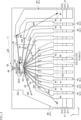
- H10W72/5449—Dispositions of bond wires not being orthogonal to a side surface of the chip, e.g. fan-out arrangements
-
- H—ELECTRICITY
- H10—SEMICONDUCTOR DEVICES; ELECTRIC SOLID-STATE DEVICES NOT OTHERWISE PROVIDED FOR
- H10W—GENERIC PACKAGES, INTERCONNECTIONS, CONNECTORS OR OTHER CONSTRUCTIONAL DETAILS OF DEVICES COVERED BY CLASS H10
- H10W72/00—Interconnections or connectors in packages
- H10W72/50—Bond wires
- H10W72/541—Dispositions of bond wires
- H10W72/547—Dispositions of multiple bond wires
-
- H—ELECTRICITY
- H10—SEMICONDUCTOR DEVICES; ELECTRIC SOLID-STATE DEVICES NOT OTHERWISE PROVIDED FOR
- H10W—GENERIC PACKAGES, INTERCONNECTIONS, CONNECTORS OR OTHER CONSTRUCTIONAL DETAILS OF DEVICES COVERED BY CLASS H10
- H10W74/00—Encapsulations, e.g. protective coatings
- H10W74/40—Encapsulations, e.g. protective coatings characterised by their materials
-
- H—ELECTRICITY
- H10—SEMICONDUCTOR DEVICES; ELECTRIC SOLID-STATE DEVICES NOT OTHERWISE PROVIDED FOR
- H10W—GENERIC PACKAGES, INTERCONNECTIONS, CONNECTORS OR OTHER CONSTRUCTIONAL DETAILS OF DEVICES COVERED BY CLASS H10
- H10W90/00—Package configurations
- H10W90/701—Package configurations characterised by the relative positions of pads or connectors relative to package parts
- H10W90/751—Package configurations characterised by the relative positions of pads or connectors relative to package parts of bond wires
- H10W90/753—Package configurations characterised by the relative positions of pads or connectors relative to package parts of bond wires between laterally-adjacent chips
-
- H—ELECTRICITY
- H10—SEMICONDUCTOR DEVICES; ELECTRIC SOLID-STATE DEVICES NOT OTHERWISE PROVIDED FOR
- H10W—GENERIC PACKAGES, INTERCONNECTIONS, CONNECTORS OR OTHER CONSTRUCTIONAL DETAILS OF DEVICES COVERED BY CLASS H10
- H10W90/00—Package configurations
- H10W90/701—Package configurations characterised by the relative positions of pads or connectors relative to package parts
- H10W90/751—Package configurations characterised by the relative positions of pads or connectors relative to package parts of bond wires
- H10W90/755—Package configurations characterised by the relative positions of pads or connectors relative to package parts of bond wires between a chip and a laterally-adjacent insulating package substrate, interpose or RDL
Definitions
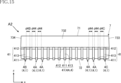
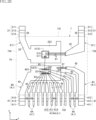
- the third root portion 412 is the root portion of the third outer portion 41. As shown in FIGS. 1 and 2, the third root portion 412 is located at the end of the third outer portion 41 on the sealing resin 7 side in the first direction y. The third root portion 412 is located closer to the sealing resin 7 than the third mounting portion 411 and the third relay portion 413 in the first direction y. The third root portion 412 is located above the third mounting portion 411 in the thickness direction z, and protrudes from the central portion of the sealing resin 7 in the thickness direction z. The plurality of third root portions 412 are arranged at the same (or substantially the same) position in the thickness direction z.
- the dimensions W41B and W41C are the same (or substantially the same) as the dimension W21 of the first outer part 21 and the dimension W31 of the second outer part 31, respectively.
- the dimension (width) along the second direction x of the part (boundary 49 part) where the third outer part 41 and the third inner part 42 are connected is, for example, 0. It is 15 mm or more and 0.5 mm or less.
- the width of the boundary 49 portion of each inner lead 4A is the same (or substantially the same) as the dimension W41A of the third outer portion 41 of each inner lead 4A.
- the wire 61 is joined to the electrode 511 of the first chip 51 and the second inner part 32, and electrically connects the first chip 51 and the second lead 3. That is, the second outer part 31 of the second lead 3 is electrically connected to the first chip 51 of the electronic component 5 via the second inner part 32 and the wire 61.
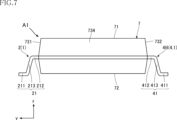
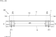
- the resin main surface 71 and the resin back surface 72 are spaced apart from each other in the thickness direction z.
- the resin main surface 71 faces one direction in the thickness direction z, and the resin back surface 72 faces the other direction in the thickness direction z.
- the main resin surface 71 is the upper surface of the sealing resin 7
- the resin back surface 72 is the lower surface of the sealing resin 7 .
- the length of the wire 61 is 65% or less of the average value of the distance d11 and the distance d12 in plan view. According to this configuration, it is possible to suppress an increase in the size of the electronic device A1 (an increase in the size of the sealing resin 7). Therefore, the electronic device A1 suppresses deformation or disconnection of the wire 61 by setting the length of the wire 61 in a plan view to 25% or more and 65% or less of the average value of the distance d11 and the distance d12. Enlargement of the electronic device A1 (enlargement of the sealing resin 7) can be suppressed.
- the electronic component 5 of the electronic device A3 has a power conversion function rather than a voltage detection function.
- the first chip 51 and the second chip 52 in this embodiment are each switching elements.
- each of the first chip 51 and the second chip 52 is configured with an IGBT (Insulated Gate Bipolar Transistor), but instead of an IGBT, it is a MOSFET (Metal-Oxide-Semiconductor Field). Effect Transistor) or other transistors such as bipolar transistors.
- the plurality of wires 64 are respectively joined to the electrode 522 and the second inner part 32 of the second lead 3 to electrically connect them. Thereby, the second lead 3 is electrically connected to the electrode 522 via the plurality of wires 64.
- the sealing resin has a second resin side face facing the other side of the first direction,
Landscapes
- Lead Frames For Integrated Circuits (AREA)
- Engineering & Computer Science (AREA)
- Microelectronics & Electronic Packaging (AREA)
- Physics & Mathematics (AREA)
- Geometry (AREA)
Priority Applications (2)
| Application Number | Priority Date | Filing Date | Title |
|---|---|---|---|
| JP2024507644A JPWO2023176332A1 (https=) | 2022-03-17 | 2023-02-21 | |
| US18/883,587 US20250006621A1 (en) | 2022-03-17 | 2024-09-12 | Electronic device |
Applications Claiming Priority (2)
| Application Number | Priority Date | Filing Date | Title |
|---|---|---|---|
| JP2022043110 | 2022-03-17 | ||
| JP2022-043110 | 2022-03-17 |
Related Child Applications (1)
| Application Number | Title | Priority Date | Filing Date |
|---|---|---|---|
| US18/883,587 Continuation US20250006621A1 (en) | 2022-03-17 | 2024-09-12 | Electronic device |
Publications (1)
| Publication Number | Publication Date |
|---|---|
| WO2023176332A1 true WO2023176332A1 (ja) | 2023-09-21 |
Family
ID=88023338
Family Applications (1)
| Application Number | Title | Priority Date | Filing Date |
|---|---|---|---|
| PCT/JP2023/006238 Ceased WO2023176332A1 (ja) | 2022-03-17 | 2023-02-21 | 電子装置 |
Country Status (3)
| Country | Link |
|---|---|
| US (1) | US20250006621A1 (https=) |
| JP (1) | JPWO2023176332A1 (https=) |
| WO (1) | WO2023176332A1 (https=) |
Cited By (1)
| Publication number | Priority date | Publication date | Assignee | Title |
|---|---|---|---|---|
| WO2025164246A1 (ja) * | 2024-01-31 | 2025-08-07 | ローム株式会社 | 半導体装置 |
Citations (2)
| Publication number | Priority date | Publication date | Assignee | Title |
|---|---|---|---|---|
| JP2004047955A (ja) * | 2002-05-22 | 2004-02-12 | Matsushita Electric Ind Co Ltd | 半導体装置 |
| JP2016207714A (ja) * | 2015-04-16 | 2016-12-08 | ローム株式会社 | 半導体装置 |
-
2023
- 2023-02-21 WO PCT/JP2023/006238 patent/WO2023176332A1/ja not_active Ceased
- 2023-02-21 JP JP2024507644A patent/JPWO2023176332A1/ja active Pending
-
2024
- 2024-09-12 US US18/883,587 patent/US20250006621A1/en active Pending
Patent Citations (2)
| Publication number | Priority date | Publication date | Assignee | Title |
|---|---|---|---|---|
| JP2004047955A (ja) * | 2002-05-22 | 2004-02-12 | Matsushita Electric Ind Co Ltd | 半導体装置 |
| JP2016207714A (ja) * | 2015-04-16 | 2016-12-08 | ローム株式会社 | 半導体装置 |
Cited By (1)
| Publication number | Priority date | Publication date | Assignee | Title |
|---|---|---|---|---|
| WO2025164246A1 (ja) * | 2024-01-31 | 2025-08-07 | ローム株式会社 | 半導体装置 |
Also Published As
| Publication number | Publication date |
|---|---|
| US20250006621A1 (en) | 2025-01-02 |
| JPWO2023176332A1 (https=) | 2023-09-21 |
Similar Documents
| Publication | Publication Date | Title |
|---|---|---|
| JP4459883B2 (ja) | 半導体装置 | |
| US6787889B2 (en) | Multilevel leadframe for a packaged integrated circuit and method of fabrication | |
| US10283699B2 (en) | Hall-effect sensor isolator | |
| US20080079124A1 (en) | Interdigitated leadfingers | |
| US11538743B2 (en) | Microelectronic device with floating pads | |
| CN115315763A (zh) | 检流电阻器以及电流检测装置 | |
| JP2016195223A (ja) | 半導体装置及びその製造方法 | |
| CN110473860B (zh) | 具有集成分流电阻器的半导体器件及其制造方法 | |
| WO2023176332A1 (ja) | 電子装置 | |
| US20240332138A1 (en) | Electronic device | |
| US11296073B2 (en) | Semiconductor device | |
| US10490489B2 (en) | Conductive clip connection arrangements for semiconductor packages | |
| US12582016B2 (en) | Semiconductor device | |
| JP4695041B2 (ja) | 半導体装置 | |
| JPH0897255A (ja) | 電力用半導体装置 | |
| US20120217655A1 (en) | Electronic device for high power applications | |
| WO2025009349A1 (ja) | 電子装置 | |
| US20250293126A1 (en) | Electronic device | |
| JP5151537B2 (ja) | パワー半導体素子 | |
| WO2024095795A1 (ja) | 電子装置 | |
| US20240332137A1 (en) | Electronic device | |
| US20120056240A1 (en) | Semiconductor device | |
| JP3311935B2 (ja) | 半導体装置およびその計測方法 | |
| US20250079272A1 (en) | Semiconductor device and manufacturing method | |
| CN118525371A (zh) | 电子装置 |
Legal Events
| Date | Code | Title | Description |
|---|---|---|---|
| 121 | Ep: the epo has been informed by wipo that ep was designated in this application |
Ref document number: 23770291 Country of ref document: EP Kind code of ref document: A1 |
|
| ENP | Entry into the national phase |
Ref document number: 2024507644 Country of ref document: JP Kind code of ref document: A |
|
| NENP | Non-entry into the national phase |
Ref country code: DE |
|
| 122 | Ep: pct application non-entry in european phase |
Ref document number: 23770291 Country of ref document: EP Kind code of ref document: A1 |