WO2023171525A1 - 固体電解コンデンサ - Google Patents
固体電解コンデンサ Download PDFInfo
- Publication number
- WO2023171525A1 WO2023171525A1 PCT/JP2023/007806 JP2023007806W WO2023171525A1 WO 2023171525 A1 WO2023171525 A1 WO 2023171525A1 JP 2023007806 W JP2023007806 W JP 2023007806W WO 2023171525 A1 WO2023171525 A1 WO 2023171525A1
- Authority
- WO
- WIPO (PCT)
- Prior art keywords
- metal foil
- end surface
- sheet
- layer
- adhesive resin
- Prior art date
- Legal status (The legal status is an assumption and is not a legal conclusion. Google has not performed a legal analysis and makes no representation as to the accuracy of the status listed.)
- Ceased
Links
Images





Classifications
-
- H—ELECTRICITY
- H01—ELECTRIC ELEMENTS
- H01G—CAPACITORS; CAPACITORS, RECTIFIERS, DETECTORS, SWITCHING DEVICES, LIGHT-SENSITIVE OR TEMPERATURE-SENSITIVE DEVICES OF THE ELECTROLYTIC TYPE
- H01G9/00—Electrolytic capacitors, rectifiers, detectors, switching devices, light-sensitive or temperature-sensitive devices; Processes of their manufacture
- H01G9/004—Details
- H01G9/04—Electrodes or formation of dielectric layers thereon
- H01G9/048—Electrodes or formation of dielectric layers thereon characterised by their structure
-
- H—ELECTRICITY
- H01—ELECTRIC ELEMENTS
- H01G—CAPACITORS; CAPACITORS, RECTIFIERS, DETECTORS, SWITCHING DEVICES, LIGHT-SENSITIVE OR TEMPERATURE-SENSITIVE DEVICES OF THE ELECTROLYTIC TYPE
- H01G9/00—Electrolytic capacitors, rectifiers, detectors, switching devices, light-sensitive or temperature-sensitive devices; Processes of their manufacture
- H01G9/004—Details
- H01G9/08—Housing; Encapsulation
-
- H—ELECTRICITY
- H01—ELECTRIC ELEMENTS
- H01G—CAPACITORS; CAPACITORS, RECTIFIERS, DETECTORS, SWITCHING DEVICES, LIGHT-SENSITIVE OR TEMPERATURE-SENSITIVE DEVICES OF THE ELECTROLYTIC TYPE
- H01G9/00—Electrolytic capacitors, rectifiers, detectors, switching devices, light-sensitive or temperature-sensitive devices; Processes of their manufacture
- H01G9/004—Details
- H01G9/08—Housing; Encapsulation
- H01G9/10—Sealing, e.g. of lead-in wires
-
- H—ELECTRICITY
- H01—ELECTRIC ELEMENTS
- H01G—CAPACITORS; CAPACITORS, RECTIFIERS, DETECTORS, SWITCHING DEVICES, LIGHT-SENSITIVE OR TEMPERATURE-SENSITIVE DEVICES OF THE ELECTROLYTIC TYPE
- H01G9/00—Electrolytic capacitors, rectifiers, detectors, switching devices, light-sensitive or temperature-sensitive devices; Processes of their manufacture
- H01G9/15—Solid electrolytic capacitors
Definitions
- the present invention relates to a solid electrolytic capacitor.
- Patent Document 1 describes (A) a step of preparing a first sheet; (B) a step of preparing a second sheet; (C) a step of covering the first sheet with an insulating material; (D) a step of the above. Step of forming a conductor layer on the first sheet; (E) Step of producing a laminated sheet; (F) Step of producing a laminated block; (G) Cutting the above-mentioned laminated block; A method for manufacturing a solid electrolytic capacitor, comprising a step of manufacturing an element laminate; and (H) a step of forming a first external electrode and a second external electrode, and a solid electrolytic capacitor manufactured by the manufacturing method, Disclosed.
- a valve-acting metal base having a dielectric layer formed on the surface and a metal foil are laminated with a solid electrolyte layer interposed therebetween.
- a capacitor element is formed, and the periphery of the capacitor element is sealed with a sealing material except for the connection portion with the external electrode.
- a gap is generated between the valve metal base or metal foil and the sealing material, which may deteriorate the sealing performance of the solid electrolytic capacitor.
- the present invention was made to solve the above problems, and an object of the present invention is to provide a solid electrolytic capacitor with excellent sealing properties.
- the solid electrolytic capacitor of the present invention is a solid electrolytic capacitor comprising an element laminate, a first external electrode, and a second external electrode, and in the element laminate, the first layer and the second layer are are laminated via an adhesive resin, the first layer comprises a valve metal base on which a dielectric layer is formed, and a solid electrolyte layer provided on the dielectric layer, and the second layer is made of metal foil, and further, in the element laminate, the metal foil and the first sealing portion are provided on the first end surface of the first end surface and the second end surface facing each other in the length direction.
- the second external electrode is connected to the metal foil, and the second external electrode is provided on the second end surface of the element laminate and is connected to the valve metal base, and the first sealing part is connected to the valve metal base.
- the section includes a second columnar part that penetrates the valve metal base in the stacking direction, and a second band part that is provided between the valve metal base and connects the second columnar parts.
- the adhesive resin has less filler than the first sealing part and the second sealing part, and the adhesive resin has less filler than the first sealing part and the second sealing part, and the metal foil and the first columnar part have a smaller amount of filler than the first sealing part and the second sealing part.
- a solid electrolytic capacitor with excellent sealing properties can be provided.
- FIG. 1 is a cross-sectional view schematically showing an example of a solid electrolytic capacitor according to a first embodiment of the present invention.
- FIG. 2A is a perspective view of the solid electrolytic capacitor shown in FIG. 1 viewed from the first end surface side.
- FIG. 2B is a perspective view of the solid electrolytic capacitor shown in FIG. 1 viewed from the second end surface side.
- FIG. 3 is an enlarged plan view of the first end surface of the element stack constituting the solid electrolytic capacitor shown in FIG.
- FIG. 4 is an enlarged plan view of the second end surface of the element stack constituting the solid electrolytic capacitor shown in FIG.
- FIG. 5A is a diagram schematically showing the inside of the element stack shown in FIG. 3 as seen through from the first end surface side.
- FIG. 5B is a cross-sectional view taken along the line X1-X1 of the element stack shown in FIG. 5A.
- FIG. 5C is a cross-sectional view taken along the line X2-X2 of the element stack shown in FIG. 5A.
- FIG. 6A is a diagram schematically showing the inside of the element stack shown in FIG. 4 as seen through from the second end surface side.
- FIG. 6B is a cross-sectional view taken along the line X3-X3 of the element stack shown in FIG. 6A.
- FIG. 6C is a cross-sectional view taken along the line X4-X4 of the element stack shown in FIG. 6A.
- FIG. 7 is a plan view showing a modification of the first end surface shown in FIG. 3.
- FIG. 8 is a plan view showing a modification of the second end face shown in FIG. 4.
- FIG. FIG. 9A is a perspective view schematically showing an example of the first sheet.
- FIG. 9B is an enlarged perspective view of a portion of the first sheet shown in FIG. 9A.
- FIG. 10A is a perspective view schematically showing an example of the second sheet.
- FIG. 10B is an enlarged perspective view of a portion of the second sheet shown in FIG. 10A.
- FIG. 11A is a perspective view schematically showing an example of a first sheet provided with adhesive resin.
- FIG. 11B is an enlarged perspective view of a portion of the first sheet shown in FIG. 11A.
- FIG. 12A is a perspective view schematically showing an example of a first sheet provided with an adhesive resin and a conductive layer.
- FIG. 12B is an enlarged perspective view of a portion of the first sheet shown in FIG. 12A.
- FIG. 13A is a perspective view schematically showing an example of a state before the first sheet and the second sheet are laminated.
- FIG. 13B is a perspective view schematically showing an example of a laminated sheet.
- FIG. 14A is a perspective view schematically showing an example of a laminated block body.
- FIG. 14B is a partially exploded and enlarged perspective view of the laminated block body shown in FIG. 14A.
- FIG. 15A is a plan view schematically showing the valve metal base before cutting.
- FIG. 15B is a plan view schematically showing the valve metal base after cutting.
- FIG. 16A is a plan view schematically showing the metal foil before cutting.
- FIG. 16B is a plan view schematically showing the metal foil after cutting.
- FIG. 17 is a cross-sectional view schematically showing an example of an element stack.
- FIG. 18A is a perspective view of the element stack shown in FIG. 17 viewed from the first end surface side.
- FIG. 18B is a perspective view of the element stack shown in FIG. 17 viewed from the second end surface side.
- FIG. 19A is a perspective view schematically showing an example of a laminated block body after being cut.
- FIG. 19B is a partially exploded and enlarged perspective view of the laminated block body shown in FIG. 19A.
- FIG. 20A is a perspective view schematically showing an example of a laminated block body in which a fourth sealing portion is formed.
- FIG. 20B is a partially exploded and enlarged perspective view of the laminated block body shown in FIG. 20A.
- FIG. 21A is a perspective view schematically showing an example of a singulated element stack.
- FIG. 21B is a partially exploded and enlarged perspective view of the element stack shown in FIG. 21A.
- FIG. 22A is a perspective view schematically showing an example of a first sheet provided with adhesive resin.
- FIG. 22B is an enlarged perspective view of a portion of the first sheet shown in FIG. 22A.
- FIG. 23A is a perspective view schematically showing an example of a state before the first sheet and the second sheet are laminated.
- FIG. 23B is a perspective view schematically showing an example of a laminated sheet.
- FIG. 24A is a perspective view schematically showing an example of a laminated block body.
- FIG. 24B is a partially exploded and enlarged perspective view of the laminated block body shown in FIG. 24A.
- the solid electrolytic capacitor of the present invention will be explained below.
- the present invention is not limited to the following configuration, and can be modified and applied as appropriate without changing the gist of the present invention.
- the present invention also includes a combination of two or more of the individual desirable configurations described below.
- FIG. 1 is a cross-sectional view schematically showing an example of a solid electrolytic capacitor according to a first embodiment of the present invention.
- the solid electrolytic capacitor 1 shown in FIG. 1 includes an element stack 100, a first external electrode 141, and a second external electrode 142.
- the element stack 100 includes a valve metal base 11 having a porous portion (not shown) on its surface, a dielectric layer 12 formed on the surface of the porous portion, and a dielectric layer 12 formed on the surface of the porous portion.
- a first layer 110 comprising a solid electrolyte layer 13 provided on the body layer 12 and a second layer 120 comprising a metal foil 21 are laminated via an adhesive resin (not shown).
- a mask layer (not shown) is provided on the dielectric layer 12 around the solid electrolyte layer 13, and an adhesive resin is placed on the mask layer (between the mask layer and the metal foil 21) on the same plane as the mask layer. It is set in shape. Furthermore, a conductor layer (not shown) is provided between the solid electrolyte layer 13 and the metal foil 21.
- the first end surface E101 is coated with metal foil. 21 and the first sealing portion 131 are exposed, and the valve metal base 11 and the second sealing portion 132 are exposed on the second end surface E102.
- the dielectric layer 12 is also exposed on the second end surface E102 of the element stack 100, in the following description, it will simply be referred to as "the valve metal base 11 and the second sealing part 132 are exposed”. It is written as
- the first external electrode 141 is provided on the first end surface E101 of the element stack 100 and connected to the metal foil 21, and the second external electrode 142 is provided on the second end surface E102 of the element stack 100. and is connected to the valve metal base 11.
- FIG. 2A is a perspective view of the solid electrolytic capacitor shown in FIG. 1 viewed from the first end surface side.
- FIG. 2B is a perspective view of the solid electrolytic capacitor shown in FIG. 1 viewed from the second end surface side.
- FIG. 3 is an enlarged plan view of the first end surface of the element stack constituting the solid electrolytic capacitor shown in FIG.
- FIG. 4 is an enlarged plan view of the second end surface of the element stack constituting the solid electrolytic capacitor shown in FIG. Note that FIG. 1 is a cross-sectional view taken along line AA of the element stack shown in FIG. 2A.
- the element stack 100 has a first main surface M101 and a second main surface M102 facing each other in the stacking direction (T direction), and a length direction perpendicular to the stacking direction.
- a first end surface E101 and a second end surface E102 facing each other in the L direction, and a first side surface S101 and a second side surface S102 facing each other in the width direction (W direction) perpendicular to the stacking direction and the length direction. has.
- the element stack 100 further includes a third sealing part 133 that covers the respective main surfaces M101 and M102, and a fourth sealing part 134 that covers the respective side surfaces S101 and S102.
- the third sealing portion 133 may cover at least one main surface M101 and/or M102 of the element stack 100.
- the first sealing part 131 is provided between a first columnar part 131a that penetrates the metal foil 21 in the stacking direction and the first columnar part 131a. and a first band-shaped portion 131b connecting between the two.
- the second sealing part 132 is provided between the second columnar part 132a that penetrates the valve metal base 11 in the stacking direction and the valve metal base 11, and and a second strip portion 132b connecting the columnar portions 132a.
- the metal foil 21 has a rectangular shape with a plurality of notches 21a (the same number for the plurality of stacked metal foils 21) on one side of the first end surface E101.
- a plurality of valve metal bases 11 are arranged on one side of the second columnar portion 132a (however, the same number of valve metal bases 11 are stacked on each other). It has a rectangular shape with a number of notches 11a provided therein. It is preferable that the notches 11a and 21a are arranged at equal intervals in the width direction. Note that, although both the cutout portions 11a and 21a are semicircular, the shapes thereof are not particularly limited.
- FIG. 5A is a diagram schematically showing the inside of the element stack shown in FIG. 3 as seen through from the first end surface side.
- FIG. 5B is a cross-sectional view taken along the line X1-X1 of the element stack shown in FIG. 5A.
- FIG. 5C is a cross-sectional view taken along the line X2-X2 of the element stack shown in FIG. 5A.
- FIG. 6A is a diagram schematically showing the inside of the element stack shown in FIG. 4 as seen through from the second end surface side.
- FIG. 6B is a cross-sectional view taken along the line X3-X3 of the element stack shown in FIG. 6A.
- FIG. 6C is a cross-sectional view taken along the line X4-X4 of the element stack shown in FIG. 6A.
- the adhesive resin 15 for bonding the first layer 110 and the second layer 120 is present in the first region between the metal foil 21 and the first columnar portion 131a inside the element stack 100 (see FIG. 5A and 5B), in the second region between the valve metal base 11 and the first strip 131b (see FIGS. 5A and 5C). Furthermore, the adhesive resin 15 is present in the third region between the valve metal base 11 and the second columnar portion 132a inside the element laminate 100 (see FIGS. 6A and 6C), and the metal foil 21 and the fourth region between the second strip portion 132b (see FIGS. 6A and 6B). Furthermore, the adhesive resin 15 has less filler, that is, is richer in resin, than the first sealing part 131 and the second sealing part 132.
- the adhesive resin 15 has higher flexibility than the first sealing part 131 and the second sealing part 132. In this way, a highly flexible adhesive resin is used between the metal foil 21 and the first sealing part 131 and between the valve metal base 11 and the second sealing part 132 inside the element laminate 100. 15, it is possible to suppress the generation of gaps between them. Therefore, the sealing performance of the solid electrolytic capacitor 1 is improved.
- the adhesive resin has less filler than the first sealing part can be determined by, for example, any cross section of the solid electrolytic capacitor (however, the adhesive resin and the first sealing part are exposed). This can be confirmed by observing the cross section (the same applies below). Furthermore, the accuracy of confirmation may be improved by averaging the results obtained by changing the observation location for a plurality of arbitrary cross sections of the solid electrolytic capacitor.
- the cross section was elementally mapped using SEM-EDX, and based on the mapping area of resin components (C, O, H) and different metal components (Si, Al, etc.) around the adhesive resin and the signal strength of EDX,
- the accuracy of confirmation can also be improved by clarifying the target elements of each of the first sealing part and the first sealing part and investigating the difference. It is also possible to confirm whether "the adhesive resin contains less filler than the second sealing part" by the same method.
- the adhesive resin 15 may be present in at least one of the first region, the second region, the third region, and the fourth region inside the element stack 100.
- the adhesive resin 15 is preferably present in at least one of the first region and the third region inside the element stack 100; More preferably, it exists in the region.
- the adhesive resin 15 When the adhesive resin 15 is present in the first region, the adhesive resin 15 is present between the end surface of the at least one metal foil 21 constituting at least one notch 21a and the first columnar section 131a. It turns out. In addition, when the adhesive resin 15 exists in the third region, the adhesive resin 15 is attached to the end face constituting at least one notch portion 11a of the at least one valve metal base 11 and the second columnar portion 132a. will exist between.
- the metal foil 21 has an end surface 21b (that is, an end surface forming the notch portion 21a) facing the first columnar portion 131a (see FIGS. 5A and 5B), and the valve metal base 11 has an end surface 21b facing the first columnar portion 131a (see FIGS. 5A and 5B). It has an end surface 11b (that is, an end surface forming the notch portion 11a) facing the portion 132a (see FIGS. 6A and 6C).
- the end surface 21b and the end surface 11b are end surfaces located inside the element stack 100 and not exposed to the first end surface E101 and the second end surface E102, respectively.
- the adhesive resin 15 covers the entire end surface 21b of the metal foil 21 (see FIGS. 5A and 5B, especially the center end surface 21b in FIG. 5B), and the adhesive resin 15 covers the entire end surface 21b of the metal foil 21. It is preferable to cover the entire end surface 11b of 11 (see FIGS. 6A and 6C, especially the center end surface 11b in FIG. 6C).
- the adhesive resin 15 covers the entire end surface 21b of the metal foil 21 means that the adhesive resin 15 covers the entire at least one end surface 21b of the at least one metal foil 21. The same applies when the adhesive resin 15 covers the entire end surface 11b of the valve metal base 11.
- the adhesive resin 15 may cover only one of the entire end surface 21b of the metal foil 21 and the entire end surface 11b of the valve metal base 11.
- FIG. 7 is a plan view showing a modification of the first end surface shown in FIG. 3.
- FIG. 8 is a plan view showing a modification of the second end face shown in FIG. 4.
- the adhesive resin 15 may be exposed from the inside of the element stack 100 to the first end surface E101, as shown in FIG. It may be exposed at the end surface E102.
- shear stress that leads to interfacial peeling is generated on the first end surface E101 and the second end surface E102, but this shear stress is alleviated by the exposed adhesive resin 15. be able to. Therefore, the occurrence of a peeling interface (gap) between the metal foil 21 and the first sealing part 131 can be suppressed, and the separation between the valve metal base 11 and the dielectric layer 12 and the second sealing part 132 can be suppressed. It is possible to suppress the occurrence of a peeling interface (gap) between the two.
- the sealing performance of the solid electrolytic capacitor 1 is further improved. Furthermore, when the first external electrode 141 and the second external electrode 142 are formed by plating, it is possible to prevent the plating solution from entering through the gaps, so that the plating solution that has entered the inside of the element stack 100 can be prevented. LC defects due to precipitation of metal ions inside can be reduced. Furthermore, since moisture in the air can be prevented from entering through the gap, corrosion of the metal foil 21 and the valve metal base 11 due to moisture can be reduced, and LC defects can be improved.
- the adhesive resin 15 may be exposed from the inside of the element stack 100 to only one of the first end surface E101 and the second end surface E102. Furthermore, when the adhesive resin 15 is exposed to the first end surface E101 and/or the second end surface E102, the adhesive resin 15 is normally applied from the inside of the element laminate 100 to the first end surface E101 and the second end surface E102. exposed only to a portion of at least one side of the
- the adhesive resin 15 does not contain filler.
- the adhesive strength of the adhesive resin 15 is improved, and generation of gaps inside the element stack 100 can be more effectively suppressed. This is because the filler does not have an adhesive function, and only the resin has an adhesive function.
- the Poisson's ratio of the adhesive resin 15 is preferably 0.3 or more, and preferably 0.4 or more. This increases the deformation of the adhesive resin 15, thereby making it possible to further alleviate the shear stress during the above-mentioned cutting into pieces.
- the Poisson's ratio of the adhesive resin 15 can be measured with a microhardness meter. That is, by pressing an indenter (for example, a triangular pyramid indenter made of diamond) into the target region (adhesive resin 15), Poisson's ratio can be measured from the elastic recovery behavior upon unloading.
- an indenter for example, a triangular pyramid indenter made of diamond
- the metal foil 21 and the first sealing portion 131 are exposed on the first end surface E101 of the element stack 100. It is preferable that the sum A1 of the distances A11, A12, A13, and A14 per layer in which the metal foil 21 is exposed to the first end surface E101 in the width direction is smaller than the maximum width B1 of the metal foil 21.
- valve metal base 11 and the second sealing portion 132 are exposed on the second end surface E102 of the element stack 100.
- the sum A2 of the distances A21, A22, A23, and A24 per layer in which the valve metal base 11 is exposed to the second end surface E102 in the width direction is preferably smaller than the maximum width B2 of the valve metal base 11. .
- the value of A1/B1 is preferably 0.1 or more and 0.9 or less, and more preferably 0.5 or more.
- the value of A2/B2 is preferably 0.1 or more and 0.9 or less, and more preferably 0.5 or more.
- A1 may be the same as or different from the value of A2.
- B1 may be the same as or different from the value of B2. Therefore, the value of A1/B1 may be the same as the value of A2/B2, or may be different.
- the first sealing part 131 and the second sealing part 132 are formed by filling the through hole with a sealing material. Therefore, it is preferable that the first columnar part 131a and the first strip part 131b are integrally formed, and the second columnar part 132a and the second strip part 132b are integrally formed. . Note that "integrally formed" means that there is no interface between the two.
- the first columnar part 131a and the second columnar part 132a are It is preferable that two or more are formed.
- the first columnar part 131a and the second columnar part 132a are each provided linearly from the first main surface M101 to the second main surface M102 of the element stack 100. preferable.
- each of the columnar parts 131a and 132a is not particularly limited, but is preferably 10% or more and 70% or less of the maximum width of the metal foil 21 or the valve metal base 11.
- the maximum width of the metal foil 21 or the valve metal base 11 is 3 mm, it is preferable to arrange three columnar parts each having a width of 0.5 mm. In this case, the distance between the columnar parts is preferably 0.35 mm.
- first columnar portions 131a and two or more second columnar portions 132a are formed, it is preferable that these columnar portions are formed at equal intervals in consideration of the fillability of the sealing material. Note that “equally spaced” does not necessarily mean that the widths of the strips located between the columnar parts are exactly equal, but may be within a range of about 3%.
- the width of the band-shaped portion located between the columnar portions is not particularly limited, it is preferably 10% or more and 70% or less of the maximum width of the metal foil 21 or the valve metal base 11.
- the width of the strip portion not located between the columnar portions is approximately the same as the width of the strip portion located between the columnar portions.
- a third sealing part 133 can be formed at the same time. Therefore, the third sealing part 133 that covers at least one main surface M101 and/or M102 of the element stack 100 is formed integrally with the first sealing part 131 and the second sealing part 132. It is preferable that
- the valve metal base 11 and the metal foil 21 are connected via another conductor layer provided on the solid electrolyte layer 13.
- the connection may be made via a conductive adhesive layer provided on the conductor layer.
- the conductor layer may be comprised only of a carbon layer, may be comprised only of a silver layer, or may be comprised of two layers: a carbon layer as a base and a silver layer thereon.
- a carbon layer is provided on the solid electrolyte layer 13 as a conductive layer, and that the surface of the metal foil 21 is in direct contact with the carbon layer, and that the surface of the carbon-coated metal foil 21 is preferably in direct contact with the carbon layer. More preferred.
- valve metal base 11 and the metal foil 21 are preferably connected via the adhesive resin 15.
- FIG. 9A is a perspective view schematically showing an example of the first sheet.
- FIG. 9B is an enlarged perspective view of a portion of the first sheet shown in FIG. 9A.
- the first sheet 10 shown in FIGS. 9A and 9B has a plurality of element regions R11 (hereinafter referred to as first element regions) and a plurality of element regions R12 (hereinafter referred to as second element regions). are doing.
- the first element region R11 has a first end E11 and a second end E12 that face each other in the length direction (L direction), and a width direction ( It is divided by a first side portion S11 and a second side portion S12 that face each other in the W direction).
- the dimension in the length direction (L direction) is larger than the dimension in the width direction (W direction).
- One first through hole H1 is formed so as to straddle the first end E11 of the first element region R11 in the length direction, and the second end E11 of the first element region R11
- a plurality of second through holes H2 (three in FIG. 9B) are formed so as to straddle the portion E12 in the length direction.
- the first through hole H1 consists of one elongated hole having a width greater than or equal to the width of the first element region R11, and the second through hole H2 has a width smaller than the width of the first element region R11. It consists of a plurality of approximately round holes.
- the second element region R12 has the same shape as the first element region R11, but the orientation of the first end E11 and the second end E12 is different from that of the first element region R11. The opposite is true.
- first element regions R11 and second element regions R12 are arranged alternately in the length direction.
- the first element region R11 shares the first end E11 and the first through hole H1 with the adjacent second element region R12, and also shares the first end E11 and the first through hole H1 with the adjacent second element region R12. It shares a second end E12 and a second through hole H2 with the region R12.
- first element regions R11 and second element regions R12 are arranged alternately in the width direction.
- the first element region R11 shares a first side portion S11 with an adjacent second element region R12, and also shares a second side portion S11 with another adjacent second element region R12. They share part S12.
- the first sheet 10 includes a valve metal base 11 having a porous portion (not shown) on its surface, a dielectric layer 12 formed on the surface of the porous portion, and a dielectric layer 12 formed on the surface of the porous portion.
- a solid electrolyte layer 13 is provided inside each element region on the layer 12.
- the ends and sides of each element region are covered with a mask layer 14 made of an insulating material, and a solid electrolyte layer 13 is provided in a region surrounded by the mask layer 14.
- the valve metal base 11 has porous portions on both sides, and a dielectric layer 12 is formed on the surface of each porous portion.
- a solid electrolyte layer 13 is provided.
- the second sheet is not laminated on one side of the first sheet, it is not necessary to provide a solid electrolyte layer on the surface of the valve metal base on the side where the second sheet (metal foil) is not laminated. do not have.
- a dielectric layer and a porous portion may not be formed on the surface of the valve metal base on the side on which the second sheet (metal foil) is not laminated.
- the first sheet 10 may be one in which the valve metal base 11 has a porous portion on only one side, and the dielectric layer 12 is formed on the surface of the porous portion.
- the first sheet is preferably made as follows. First, a valve metal base 11 having a porous portion on its surface is prepared, and a dielectric layer 12 is formed on the surface of the porous portion. For example, when aluminum foil is used as the valve metal base, the surface of the aluminum foil is anodized (also called chemical conversion treatment) in an aqueous solution containing ammonium adipate, etc. to create a dielectric film made of an oxide film. layers can be formed.
- valve metal base is made of a valve metal that exhibits so-called valve action.
- valve metals include simple metals such as aluminum, tantalum, niobium, titanium, and zirconium, and alloys containing these metals. Among these, aluminum or aluminum alloy is preferred.
- the shape of the valve metal base is preferably flat, more preferably foil-like.
- the porous portion include an etching layer formed on the surface of the valve metal base, and a porous layer formed on the surface of the valve metal base by printing and sintering.
- an etched layer is preferred, and when the valve metal is titanium or a titanium alloy, a porous layer is preferred.
- the thickness of the valve metal base is not particularly limited, but the thickness of the portion excluding the porous portion is preferably 5 ⁇ m or more and 100 ⁇ m or less. Further, the thickness of the porous portion (thickness on one side) is preferably 5 ⁇ m or more and 200 ⁇ m or less.
- the dielectric layer formed on the surface of the porous portion is porous reflecting the surface condition of the porous portion, and has a finely uneven surface shape.
- the dielectric layer is preferably made of an oxide film of the valve metal.
- a chemically formed foil that has been previously subjected to a chemical conversion treatment may be used as the valve metal base on which the dielectric layer is formed.
- the mask layer is formed, for example, by applying a mask material made of an insulating material such as an insulating resin onto the surface of the valve metal base and solidifying or hardening it by heating or the like.
- the mask material is preferably applied by screen printing, dispenser application, inkjet printing, or the like.
- Insulating materials for the mask layer include, for example, polyphenylsulfone resin, polyethersulfone resin, cyanate ester resin, fluororesin (tetrafluoroethylene, tetrafluoroethylene/perfluoroalkyl vinyl ether copolymer, etc.), soluble polyimide siloxane, and Examples include insulating resins such as compositions made of epoxy resins, polyimide resins, polyamideimide resins, and derivatives or precursors thereof.
- a first through hole H1 is formed so as to straddle the first end E11 of each element region, and a second through hole H2 is formed so as to straddle the second end E12 of each element region. do.
- the first through hole and the second through hole are formed by, for example, laser processing, etching processing, punching processing, or the like.
- a solid electrolyte layer 13 is formed inside each element region on the dielectric layer 12. At this time, it is preferable to form the solid electrolyte layer 13 in a region surrounded by the mask layer 14.
- a solid electrolyte layer can be formed in a predetermined region by applying the following treatment liquid or dispersion liquid onto a dielectric layer by sponge transfer, screen printing, dispenser coating, inkjet printing, or the like.
- the solid electrolyte layer is formed by forming a polymer film of poly(3,4-ethylenedioxythiophene) or the like on the surface of the dielectric layer using a treatment liquid containing a monomer such as 3,4-ethylenedioxythiophene.
- the dielectric layer is formed by applying a dispersion of a polymer such as poly(3,4-ethylenedioxythiophene) to the surface of the dielectric layer and drying it.
- it is preferable to form the solid electrolyte layer by forming an inner layer that fills the pores (recesses) of the dielectric layer and then forming an outer layer that covers the dielectric layer.
- the material constituting the solid electrolyte layer examples include conductive polymers such as polypyrroles, polythiophenes, and polyanilines. Among these, polythiophenes are preferred, and poly(3,4-ethylenedioxythiophene) called PEDOT is particularly preferred. Further, the conductive polymer may contain a dopant such as polystyrene sulfonic acid (PSS).
- PSS polystyrene sulfonic acid
- first through hole H1 and the second through hole H2 may be formed before forming the mask layer 14 or after forming the solid electrolyte layer 13.
- the size of the entire first sheet is determined by the size, shape, number, arrangement, production capacity, etc. of the element regions, and is not particularly limited.
- the shape of the element region of the first sheet is not particularly limited, it is preferably rectangular.
- the first end and the second end may be shorter or longer than the first side and the second side.
- the shape of the first through hole is not particularly limited as long as it has a width equal to or larger than the width of the element region.
- the shape, number, arrangement, etc. of the second through holes are not particularly limited as long as they have a width smaller than the width of the element region, but two or more second through holes may be formed in the width direction in each element region. preferable. When two or more second through holes are formed, these through holes are preferably formed at equal intervals. Note that if the width of each second through hole is too small, it will be difficult to fill the sealing material in the process described later. If the ratio is too large, the ESR tends to increase because the ratio of the valve metal base exposed to the end face of the solid electrolytic capacitor becomes small.
- FIG. 10A is a perspective view schematically showing an example of the second sheet.
- FIG. 10B is an enlarged perspective view of a portion of the second sheet shown in FIG. 10A.
- the second sheet 20 shown in FIGS. 10A and 10B includes a plurality of element regions R21 (hereinafter referred to as first element regions) and a plurality of element regions R22 (hereinafter referred to as second element regions). are doing.
- the first element region R21 has a first end E21 and a second end E22 that face each other in the length direction (L direction), and a width direction ( It is divided by a first side portion S21 and a second side portion S22 that face each other in the W direction).
- a plurality of third through holes H3 (three in FIG. 10B) are formed so as to straddle the first end E21 of the first element region R21 in the length direction, and
- One fourth through hole H4 is formed so as to straddle the second end E22 of the region R21 in the length direction.
- the third through hole H3 is made up of a plurality of approximately round holes having a width smaller than the width of the first element region R21, and the fourth through hole H4 has a width greater than or equal to the width of the first element region R21. Consists of one long hole with a
- the second element region R22 has the same shape as the first element region R21, but the orientation of the first end E21 and the second end E22 is different from that of the first element region R21. The opposite is true.
- first element regions R21 and second element regions R22 are arranged alternately in the length direction.
- the first element region R21 shares a first end E21 and a third through hole H3 with an adjacent second element region R22, and also shares a first end E21 and a third through hole H3 with an adjacent second element region R22. It shares the second end E22 and the fourth through hole H4 with the region R22.
- first element regions R21 and second element regions R22 are arranged alternately in the width direction.
- the first element region R21 shares a first side portion S21 with an adjacent second element region R22, and has a second side portion S21 with another adjacent second element region R22. They share part S22.
- the second sheet 20 is made of metal foil 21.
- the second sheet is preferably made as follows. First, metal foil 21 is prepared.
- the metal foil is preferably made of at least one metal selected from the group consisting of aluminum, copper, silver, and alloys containing these metals as main components.
- the resistance value of the metal foil can be reduced and the ESR can be reduced.
- metal foil a metal foil whose surface is coated with carbon or titanium by a film forming method such as sputtering or vapor deposition may be used.
- the thickness of the metal foil is not particularly limited, but from the viewpoint of reducing ESR, it is preferably 5 ⁇ m or more and 100 ⁇ m or less.
- a roughened surface is formed on the surface of the metal foil.
- a roughened surface is formed on the surface of the metal foil, in addition to improving the adhesion between the metal foil and the solid electrolyte layer or the adhesion between the metal foil and other conductive layers, contact Since the area increases, ESR can be reduced.
- the method for forming the roughened surface is not particularly limited, and the roughened surface may be formed by etching or the like. Particularly when aluminum is used, it is preferable to apply a carbon coat or a titanium coat to the material that has been subjected to surface roughening treatment (etching treatment) in order to lower the resistance.
- a coating layer made of an anchor coating agent may be formed on the surface of the metal foil.
- a coating layer made of an anchor coating agent is formed on the surface of the metal foil, the adhesion between the metal foil and the solid electrolyte layer or the adhesion between the metal foil and other conductive layers is improved. ESR can be reduced.
- a third through hole H3 is formed so as to straddle the first end E21 of each element region, and a fourth through hole H4 is formed so as to straddle the second end E22 of each element region. do.
- the third through hole and the fourth through hole are formed by, for example, laser processing, etching processing, punching processing, or the like.
- the overall size of the second sheet is not particularly limited, but is preferably the same as the overall size of the first sheet.
- the shape, number, and arrangement of the element regions of the second sheet are preferably the same as the shape, number, and arrangement of the element regions of the opposing first sheet.
- the shape, number, arrangement, etc. of the third through holes are not particularly limited as long as they have a width smaller than the width of the element region, but two or more third through holes may be formed in the width direction in each element region. preferable. When two or more third through holes are formed, these through holes are preferably formed at equal intervals. Note that if the width of each third through hole is too small, it will be difficult to fill the sealing material in the process described later. If the ratio is too large, the ratio of the metal foil exposed on the end face of the solid electrolytic capacitor becomes small, which tends to increase ESR.
- the shape of the fourth through hole is not particularly limited as long as it has a width equal to or larger than the width of the element region.
- Step of producing a laminated sheet The first sheet and the second sheet are laminated so that the first ends and the second ends of each element region face each other. Create a sheet. In the resulting laminated sheet, the first through hole and the third through hole, and the second through hole and the fourth through hole are each communicated in the lamination direction.
- the second through hole and the third through hole are each linearly connected from the first main surface to the second main surface of the laminated sheet.
- valve metal base and the metal foil are connected through another conductor layer provided on the solid electrolyte layer.
- the valve metal base and the metal foil may be connected via a conductive adhesive layer provided on the conductor layer.
- valve metal base and the metal foil are connected via an adhesive resin.
- FIG. 11A is a perspective view schematically showing an example of a first sheet provided with adhesive resin.
- FIG. 11B is an enlarged perspective view of a portion of the first sheet shown in FIG. 11A.
- an adhesive resin (adhesive layer) 15 before solidification or hardening is provided on the mask layer 14 of the first sheet 10 shown in FIGS. 9A and 9B.
- the adhesive resin is an insulating adhesive containing at least resin, and preferably does not contain filler.
- resins included in the adhesive resin include epoxy resins and phenol resins.
- fillers that may be included in the adhesive resin include metal oxide particles such as silica particles and alumina particles.
- the adhesive resin contains filler, it contains less filler than the sealing material described below.
- the content of filler in the adhesive resin is not particularly limited, but is usually 0% by weight or more and 5% by weight or less, preferably 0% by weight or more and 15% by weight or less.
- the adhesive resin is formed by, for example, applying an insulating adhesive before solidification or hardening onto the mask layer, and solidifying or hardening it by heating or the like.
- the application of the insulating adhesive is preferably performed by screen printing, dispenser application, inkjet printing, or the like.
- this manufacturing method includes the step of (C) covering the first sheet with an insulating material.
- step (C) the first end and the second end, and the first side and the second side of each element region of the first sheet are covered with an insulating material.
- the step of covering with an insulating material preferably includes a step of forming a mask layer and a step of forming an adhesive resin on the mask layer.
- the adhesive resin may have the same components and viscosity as the mask layer, but preferably has different components and viscosity from the mask layer.
- the combined height of the mask layer and adhesive resin in the thickness direction may be the same as the height of the solid electrolyte layer in the thickness direction, but is preferably larger than the height of the solid electrolyte layer in the thickness direction.
- FIG. 12A is a perspective view schematically showing an example of a first sheet provided with an adhesive resin and a conductive layer.
- FIG. 12B is an enlarged perspective view of a portion of the first sheet shown in FIG. 12A. 12A and 12B, an adhesive resin 15 before solidification or hardening is provided on the mask layer 14 of the first sheet 10 shown in FIGS. 9A and 9B, and a conductor is provided on the solid electrolyte layer 13.
- a layer 16 is provided.
- this manufacturing method includes the step of (D) forming a conductor layer on the first sheet.
- step (D) a conductor layer is formed on the solid electrolyte layer of the first sheet.
- the conductor layer is preferably composed of only a carbon layer, but may be composed of only a silver layer, or may be composed of two layers: a carbon layer as a base and a silver layer thereon.
- the carbon layer and the silver layer can be provided, for example, by applying carbon paste and silver paste, respectively.
- the metal foil When laminating the first sheet and the second sheet, it is preferable to place the metal foil in a state where the layer located below the metal foil is viscous. Since the carbon paste, silver paste, or solid electrolyte layer is in a viscous state before being dried, it is suitable for directly placing a metal foil thereon. On the other hand, if the carbon layer, silver layer, or solid electrolyte layer that is located under the metal foil is dried, it becomes difficult to bond the metal foil. It is preferable to place
- the conductor layer may be provided on the second sheet instead of the first sheet.
- the dam resin is a solidified or hardened insulating adhesive containing at least a resin, and preferably does not contain filler.
- the dam resin can be formed using an insulating adhesive for forming the adhesive resin 15.
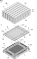
- FIG. 13A is a perspective view schematically showing an example of a state before the first sheet and the second sheet are laminated.
- FIG. 13B is a perspective view schematically showing an example of a laminated sheet.
- the first sheet 10 and the second sheet 20 are alternately laminated, and the adhesive resin 15 is solidified or cured to obtain a laminated sheet 30 shown in FIG. 13B.
- the laminated sheet 30 has a first main surface M31 and a second main surface M32 that face each other in the lamination direction (T direction). Although the adhesive resin 15 and the like are omitted in FIG.
- the adhesive resin 15 is made to protrude from between the sheet 20 and the first through hole, the second through hole, the third through hole, and/or the fourth through hole.
- first sheets 10 and five second sheets 20 are stacked, and the second sheet 20 is stacked on the first main surface M31 of the laminated sheet 30, and the second sheet 20 is stacked on the second main surface M32.
- the number of first sheets and second sheets to be laminated is not particularly limited. Furthermore, the number of first sheets and the number of second sheets may be the same or different. Therefore, either the first sheet or the second sheet may be placed on the main surface of the laminated sheet. Furthermore, when producing a laminated sheet, the first sheet and the second sheet may be laminated on a substrate made of glass epoxy resin or the like.
- Step of producing a laminated block body From at least one main surface side of the obtained laminated sheet, seal the first through hole, the third through hole, the second through hole, and the fourth through hole, respectively.
- a laminated block body is produced by filling with a retaining material.
- the first through hole and the third through hole, and the second through hole and the fourth through hole are connected in the lamination direction, so that the main surface of the laminated sheet From the side, each through hole can be filled with a sealing material.
- the first sealing part fills the first through hole and the third through hole
- the second sealing part fills the second through hole and the fourth through hole.
- a sealing portion is formed.
- the filling of the sealing material can be performed, for example, by a method such as a resin molding method.
- a third sealing part that covers at least one main surface of the laminated sheet can be formed at the same time.
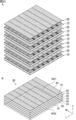
- FIG. 14A is a perspective view schematically showing an example of a laminated block body.
- FIG. 14B is a partially exploded and enlarged perspective view of the laminated block body shown in FIG. 14A.
- a first sealing part 131 that fills the first through hole H1 and the third through hole H3, and a second sealing part that fills the second through hole H2 and the fourth through hole H4.
- 132 is formed.
- the laminated block body 40 further includes a third sealing part 133 covering each main surface.
- the sealing material contains at least a resin, and preferably contains a resin and a filler.
- the resin contained in the sealing material include epoxy resin, phenol resin, and the like.
- the filler included in the sealing material include metal oxide particles such as silica particles and alumina particles.
- filler there is more filler than adhesive resin.
- the content of filler in the sealant is not particularly limited, but is usually 50% by weight or more and 95% by weight or less, preferably 80% by weight or more and 90% by weight or less.
- the maximum diameter of the filler is preferably smaller than the minimum diameters of the second through hole and the third through hole.
- the diameter of the through hole refers to the diameter when the cross section is circular, and the maximum length passing through the center of the cross section when the cross section is other than circular.
- the sealing material includes a resin and a filler
- the maximum diameter of the filler is preferably smaller than the minimum thickness of the metal foil.
- the maximum diameter of the filler included in the sealing material is preferably in the range of 20 ⁇ m or more and 50 ⁇ m or less, for example.
- (G) Step of producing a plurality of element laminates by cutting the laminate block The laminate block is cut at the first end and second end of each element region, and each A plurality of element stacks are manufactured by cutting at the positions of the first side and the second side of the element region.
- FIG. 15A is a plan view schematically showing the valve metal base before cutting.
- FIG. 15B is a plan view schematically showing the valve metal base after cutting.
- the valve metal base 11 constituting the first sheet included in the laminated block body has a first through-hole H1 that straddles the first end E11 of each element region.
- a second sealing portion 132 is formed to fill a second through hole H2 spanning the second end E12 of each element region.
- the valve metal base 11 is arranged so that the first sealing part 131 and the second sealing part 132 are separated into both sides at the positions of the first end E11 and the second end E12 of each element region.
- the first sealing portion 131 is exposed on the first end surface E101, which is the cut surface on the first end E11 side, and the valve metal base 11 is not exposed.
- the valve metal base 11 and the second sealing part 132 are exposed at the second end surface E102, which is the cut surface on the second end E12 side.
- valve metal base 11 is cut by dicing or the like at the positions of the first side S11 and second side S12 of each element region, as shown in FIG. 15B, there is valve metal on both cut surfaces. The base 11 is exposed.
- FIG. 16A is a plan view schematically showing the metal foil before cutting.
- FIG. 16B is a plan view schematically showing the metal foil after cutting.
- the metal foil 21 constituting the second sheet included in the laminated block body has a first through hole H3 filling the third through hole H3 spanning the first end E21 of each element region.
- a second sealing portion 132 is formed to fill the sealing portion 131 and the fourth through hole H4 spanning the second end E22 of each element region.
- the metal foil 21 is diced so as to separate the first sealing part 131 and the second sealing part 132 into both sides at the positions of the first end E21 and the second end E22 of each element region. As shown in FIG. 16B, the metal foil 21 and the first sealing portion 131 are exposed on the first end surface E101, which is the cut surface on the first end E21 side. On the other hand, on the second end surface E102, which is the cut surface on the second end E22 side, the second sealing portion 132 is exposed and the metal foil 21 is not exposed.
- the metal foil 21 is cut at the positions of the first side S21 and the second side S22 of each element region, the metal foil 21 is exposed on both cut surfaces, as shown in FIG. 16B.
- the first end face of the resulting element laminate is covered with metal foil and the first end.
- the sealing portion can be exposed, and the valve metal base and the second sealing portion can be exposed on the second end surface.
- both the metal foil and the valve metal base are exposed on the cut surface obtained by cutting the laminated block body at the first side and second side positions of each element region. It is preferable to form a fourth sealing part that covers each side surface of the element stack.
- FIG. 17 is a cross-sectional view schematically showing an example of an element stack.
- FIG. 18A is a perspective view of the element stack shown in FIG. 17 viewed from the first end surface side.
- FIG. 18B is a perspective view of the element stack shown in FIG. 17 viewed from the second end surface side. Note that FIG. 17 is a cross-sectional view taken along line AA of the element stack shown in FIG. 18A.
- a first layer 110 including a dielectric layer 12 and a solid electrolyte layer 13 provided on the dielectric layer 12, and a second layer 120 made of metal foil 21 are laminated.
- the first layer 110 and the second layer 120 are laminated alternately along the lamination direction (T direction), but when considering weather resistance such as moisture resistance and heat resistance, as shown in FIG. It is preferable that the second layer 120 made of metal foil is located on the outermost layer (excluding the third sealing part 133). Note that the mask layer 14, adhesive resin 15, and conductor layer 16 are omitted in FIGS. 17, 18A, and 18B.
- the metal foil 21 and the first sealing portion 131 are exposed on the first end surface E101 of the element stack 100.
- the valve metal base 11 and the second sealing portion 132 are exposed on the second end surface E102 of the element stack 100.
- the element stack 100 further includes a third sealing part 133 that covers each main surface, and a fourth sealing part 134 that covers each side surface.
- the element stack is preferably produced as follows.
- the stacked block body is cut along the first side and the second side of each element region.
- a method such as dicing using a dicer is applied, for example.
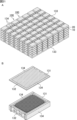
- FIG. 19A is a perspective view schematically showing an example of a laminated block body after being cut.
- FIG. 19B is a partially exploded and enlarged perspective view of the laminated block body shown in FIG. 19A.
- the first side is cut as shown in FIGS. 19A and 19B.
- a laminated block body 40a in which a gap G is formed along the second side portion is produced.
- the metal foil 21 and the valve metal base 11 are exposed on the cut side surface that appears by cutting.
- the thickness of the exposed portions of the metal foil 21 and the valve metal base 11 is greater than the thickness of the metal foil 21 and the valve metal base 11 inside which are not exposed. It is large and tapers upward and downward in the thickness direction.
- the gap formed in the stacked block body is filled with a sealing material.
- a sealing material for example, a sealing material for forming the first sealing part and the second sealing part can be used.
- FIG. 20A is a perspective view schematically showing an example of a laminated block body in which a fourth sealing portion is formed.
- FIG. 20B is a partially exploded and enlarged perspective view of the laminated block body shown in FIG. 20A.
- the stacked block body 40a shown in FIG. 19A By filling the gap G of the stacked block body 40a shown in FIG. 19A with a sealing material, the stacked block body is formed with a fourth sealing part 134 that fills the gap G, as shown in FIGS. 20A and 20B. 40b.
- the laminated block body is cut so as to separate the first sealing part 131 and the second sealing part 132 into both sides at the positions of the first end and the second end of each element region.
- the fourth sealing part 134 is cut to be separated into both sides at the positions of the first side part and the second side part of each element region. Thereby, it is possible to separate the element stack into individual pieces in which the first side portion and the second side portion are insulated by the sealing portion.
- methods such as dicing using a dicer, cutting blade, laser processing, scribing, etc. are applied.
- FIG. 21A is a perspective view schematically showing an example of a singulated element stack.
- FIG. 21B is a partially exploded and enlarged perspective view of the element stack shown in FIG. 21A.
- the laminated block body 40b shown in FIG. 20A is cut at the first end and second end of each element region, and at the first side and second side of each element region. By cutting, an element stack 100 shown in FIG. 21A is obtained. At this time, as shown in FIGS. 21A and 21B, the cut side surface that appears by cutting at the positions of the first side portion and the second side portion is configured with the fourth sealing portion 134.
- the laminated block body 40b is cut.
- the solid electrolytic capacitor 1 shown in FIG. 1 includes an element stack 100 shown in FIG. and a second external electrode 142 provided on the end surface E102.
- the first external electrode 141 is connected to the metal foil 21 exposed on the first end surface E101, and the second external electrode 142 is connected to the valve metal base 11 exposed on the second end surface E102.
- the first external electrode and the second external electrode can be formed by, for example, plating, sputtering, dip coating, printing, or the like.
- the plating layers include Zn/Ag/Ni layer, Ag/Ni layer, Ni layer, Zn/Ni/Au layer, Ni/Au layer, Zn/Ni/Cu layer, Ni/Cu layer, etc. can do. It is preferable to further form a plating layer on these plating layers, for example, in the order of a Cu plating layer, a Ni plating layer, and a Sn plating layer (or excluding some of them).
- the solid electrolytic capacitor according to the second embodiment of the present invention is substantially the same as the solid electrolytic capacitor according to the first embodiment of the present invention, except that a conductive layer is not provided between the solid electrolyte layer and the metal foil. are essentially the same. That is, the solid electrolytic capacitor according to this embodiment has the same structure as the solid electrolytic capacitor 1 shown in FIGS. 1 to 8, but in order to reduce costs and simplify the process, the valve metal base 11 and The metal foil 21 is connected to the solid electrolyte layer 13 without using any other conductive layer. In this case, the connection may be made via a conductive adhesive layer (for example, a solid electrolyte layer containing a binder) provided on the solid electrolyte layer 13.
- a conductive adhesive layer for example, a solid electrolyte layer containing a binder
- Step of preparing a first sheet First, as shown in FIGS. 9A and 9B, a first sheet is prepared in the same manner as in the first embodiment. However, the solid electrolyte layer 13 is preferably formed thicker than in the first embodiment.
- Step B Step of preparing a second sheet Separately, as shown in FIGS. 10A and 10B, a second sheet is prepared similarly to the first embodiment.
- (E) Step of producing a laminated sheet As in the first embodiment, the first sheet and the second sheet are stacked so that the first ends and the second ends of each element region face each other. A laminated sheet is produced by laminating these. In the resulting laminated sheet, the first through hole and the third through hole, and the second through hole and the fourth through hole are each communicated in the lamination direction.
- the second through hole and the third through hole are each linearly connected from the first main surface to the second main surface of the laminated sheet.
- valve metal base and the metal foil are connected without using any other conductor layer of the solid electrolyte layer.
- the valve metal base and the metal foil may be connected via a conductive adhesive layer (for example, a solid electrolyte layer containing a binder) provided on the solid electrolyte layer.
- valve metal base and the metal foil are connected via an adhesive resin.
- FIG. 22A is a perspective view schematically showing an example of a first sheet provided with adhesive resin.
- FIG. 22B is an enlarged perspective view of a portion of the first sheet shown in FIG. 22A. 22A and 22B, similar to the first embodiment, an adhesive resin (adhesive layer) 15 before solidification or hardening is provided on the mask layer 14 of the first sheet 10 shown in FIGS. 9A and 9B. It is being
- the metal foil When laminating the first sheet and the second sheet, it is preferable to place the metal foil in a state where the layer located below the metal foil is viscous. Since the solid electrolyte layer is in a viscous state before drying, it is suitable for directly placing metal foil on it. In this case, it is preferable to form the solid electrolyte layer thicker than in the first embodiment. On the other hand, if the solid electrolyte layer located under the metal foil is dried, it becomes difficult to bond the metal foil, so a conductive adhesive layer (for example, a solid electrolyte layer containing a binder) is provided on top. It is preferable to place the metal foil on the metal foil.
- a conductive adhesive layer for example, a solid electrolyte layer containing a binder
- FIG. 23A is a perspective view schematically showing an example of a state before the first sheet and the second sheet are laminated.
- FIG. 23B is a perspective view schematically showing an example of a laminated sheet.
- the first sheet 10 and the second sheet 20 are alternately laminated, and the adhesive resin 15 is solidified or hardened to form the laminated sheet shown in FIG. 23B. 30 is obtained.
- the solid electrolyte layer of the first sheet 10 and the metal foil of the second sheet 20 are connected directly or through a conductive adhesive layer provided on the solid electrolyte layer. do.
- Step of producing a laminated block body Similarly to the first embodiment, from the side of at least one main surface of the obtained laminated sheet, the first through hole, the third through hole, and the second through hole are formed.
- a laminated block body is produced by filling each of the fourth through holes with a sealing material.
- FIG. 24A is a perspective view schematically showing an example of a laminated block body.
- FIG. 24B is a partially exploded and enlarged perspective view of the laminated block body shown in FIG. 24A.
- the first through hole and the third through hole, and the second through hole and the fourth through hole are each filled with a sealing material.
- the first sealing part 131 filling the first through hole H1 and the third through hole H3, and the second through hole H2 and the fourth through hole H4 are filled.
- a second sealing portion 132 is formed for filling.
- the first sheet 10 is not provided with a conductive layer.
- the laminated block body 40 further includes a third sealing part 133 covering each main surface.
- a solid electrolytic capacitor comprising an element stack, a first external electrode, and a second external electrode
- the first layer and the second layer are laminated via an adhesive resin
- the first layer includes a valve metal base on which a dielectric layer is formed, and a solid electrolyte layer provided on the dielectric layer
- the second layer is made of metal foil, Furthermore, in the element laminate, the metal foil and the first sealing portion are exposed on the first end surface of the first end surface and the second end surface facing each other in the length direction, and the metal foil and the first sealing portion are exposed on the first end surface, and The valve metal base and the second sealing portion are exposed on the end face of the
- the first external electrode is provided on the first end surface of the element laminate and connected to the metal foil, the second external electrode is provided on the second end surface of the element laminate and connected to the valve metal base;
- the first sealing portion includes a first columnar portion that penetrates the metal foil in the stacking direction, and a first strip portion that is provided between the metal foil and connects the first columnar
- the second sealing portion is provided between a second columnar portion that penetrates the valve metal base in the stacking direction, and a second columnar portion that is provided between the valve metal base and connects the second columnar portions. having a strip-shaped portion;
- the adhesive resin has less filler than the first sealing part and the second sealing part, and has a filler content between the metal foil and the first columnar part inside the element laminate. a first region, a second region between the valve metal base and the first strip, a third region between the valve metal base and the second columnar portion, and the metal foil and a solid electrolytic capacitor present in at least one of a fourth region between the second strips.
- the adhesive resin covers at least one of the entire end surface of the metal foil facing the first columnar portion and the entire end surface of the valve metal base facing the second columnar portion. 2> or the solid electrolytic capacitor according to ⁇ 3>.
- ⁇ 5> The solid electrolytic capacitor according to any one of ⁇ 1> to ⁇ 4>, wherein the adhesive resin is exposed from inside the element laminate to at least one of the first end face and the second end face.
Landscapes
- Engineering & Computer Science (AREA)
- Power Engineering (AREA)
- Microelectronics & Electronic Packaging (AREA)
- Fixed Capacitors And Capacitor Manufacturing Machines (AREA)
- Laminated Bodies (AREA)
Priority Applications (2)
| Application Number | Priority Date | Filing Date | Title |
|---|---|---|---|
| CN202390000253.1U CN223155831U (zh) | 2022-03-07 | 2023-03-02 | 固体电解电容器 |
| JP2024506118A JP7694801B2 (ja) | 2022-03-07 | 2023-03-02 | 固体電解コンデンサ |
Applications Claiming Priority (4)
| Application Number | Priority Date | Filing Date | Title |
|---|---|---|---|
| JP2022034545 | 2022-03-07 | ||
| JP2022-034545 | 2022-03-07 | ||
| JP2023003959 | 2023-01-13 | ||
| JP2023-003959 | 2023-01-13 |
Publications (1)
| Publication Number | Publication Date |
|---|---|
| WO2023171525A1 true WO2023171525A1 (ja) | 2023-09-14 |
Family
ID=87935320
Family Applications (1)
| Application Number | Title | Priority Date | Filing Date |
|---|---|---|---|
| PCT/JP2023/007806 Ceased WO2023171525A1 (ja) | 2022-03-07 | 2023-03-02 | 固体電解コンデンサ |
Country Status (3)
| Country | Link |
|---|---|
| JP (1) | JP7694801B2 (https=) |
| CN (1) | CN223155831U (https=) |
| WO (1) | WO2023171525A1 (https=) |
Cited By (1)
| Publication number | Priority date | Publication date | Assignee | Title |
|---|---|---|---|---|
| WO2025105152A1 (ja) * | 2023-11-13 | 2025-05-22 | 株式会社村田製作所 | 固体電解コンデンサ、および固体電解コンデンサの製造方法 |
Citations (4)
| Publication number | Priority date | Publication date | Assignee | Title |
|---|---|---|---|---|
| WO2019065870A1 (ja) * | 2017-09-28 | 2019-04-04 | パナソニックIpマネジメント株式会社 | 電解コンデンサおよびその製造方法 |
| JP2019079866A (ja) * | 2017-10-20 | 2019-05-23 | 株式会社村田製作所 | 固体電解コンデンサの製造方法、及び、固体電解コンデンサ |
| JP2020194825A (ja) * | 2019-05-24 | 2020-12-03 | パナソニックIpマネジメント株式会社 | 固体電解コンデンサの製造方法 |
| JP2021080425A (ja) * | 2019-11-22 | 2021-05-27 | リンテック株式会社 | 粘着シート |
-
2023
- 2023-03-02 WO PCT/JP2023/007806 patent/WO2023171525A1/ja not_active Ceased
- 2023-03-02 CN CN202390000253.1U patent/CN223155831U/zh active Active
- 2023-03-02 JP JP2024506118A patent/JP7694801B2/ja active Active
Patent Citations (4)
| Publication number | Priority date | Publication date | Assignee | Title |
|---|---|---|---|---|
| WO2019065870A1 (ja) * | 2017-09-28 | 2019-04-04 | パナソニックIpマネジメント株式会社 | 電解コンデンサおよびその製造方法 |
| JP2019079866A (ja) * | 2017-10-20 | 2019-05-23 | 株式会社村田製作所 | 固体電解コンデンサの製造方法、及び、固体電解コンデンサ |
| JP2020194825A (ja) * | 2019-05-24 | 2020-12-03 | パナソニックIpマネジメント株式会社 | 固体電解コンデンサの製造方法 |
| JP2021080425A (ja) * | 2019-11-22 | 2021-05-27 | リンテック株式会社 | 粘着シート |
Cited By (1)
| Publication number | Priority date | Publication date | Assignee | Title |
|---|---|---|---|---|
| WO2025105152A1 (ja) * | 2023-11-13 | 2025-05-22 | 株式会社村田製作所 | 固体電解コンデンサ、および固体電解コンデンサの製造方法 |
Also Published As
| Publication number | Publication date |
|---|---|
| CN223155831U (zh) | 2025-07-25 |
| JP7694801B2 (ja) | 2025-06-18 |
| JPWO2023171525A1 (https=) | 2023-09-14 |
Similar Documents
| Publication | Publication Date | Title |
|---|---|---|
| KR102387047B1 (ko) | 고체 전해 콘덴서의 제조 방법 및 고체 전해 콘덴서 | |
| JP7408288B2 (ja) | 固体電解コンデンサ | |
| JP7067512B2 (ja) | 固体電解コンデンサ | |
| JP7063301B2 (ja) | 固体電解コンデンサの製造方法 | |
| JP7020504B2 (ja) | 固体電解コンデンサ | |
| JPWO2018074408A1 (ja) | 固体電解コンデンサ | |
| JP7259994B2 (ja) | 固体電解コンデンサ | |
| JP7226081B2 (ja) | 固体電解コンデンサの製造方法、及び、固体電解コンデンサ | |
| JP7694801B2 (ja) | 固体電解コンデンサ | |
| WO2021210367A1 (ja) | 電解コンデンサ及び電解コンデンサの製造方法 | |
| JP2020145276A (ja) | 固体電解コンデンサ | |
| JP2022095369A (ja) | 固体電解コンデンサ素子、固体電解コンデンサ、固体電解コンデンサ素子の製造方法、及び、固体電解コンデンサの製造方法 | |
| JP7501541B2 (ja) | 固体電解コンデンサ | |
| JP7419791B2 (ja) | 固体電解コンデンサ | |
| JP2024129434A (ja) | 固体電解コンデンサ及び固体電解コンデンサの製造方法 | |
| JP2025035684A (ja) | 固体電解コンデンサ及び固体電解コンデンサの製造方法 | |
| WO2026083674A1 (ja) | 固体電解コンデンサの製造方法、及び、固体電解コンデンサ | |
| WO2023171045A1 (ja) | 電解コンデンサ素子及び電解コンデンサ | |
| WO2022131020A1 (ja) | 固体電解コンデンサ素子、固体電解コンデンサ、固体電解コンデンサ素子の製造方法、及び、固体電解コンデンサの製造方法 |
Legal Events
| Date | Code | Title | Description |
|---|---|---|---|
| 121 | Ep: the epo has been informed by wipo that ep was designated in this application |
Ref document number: 23766701 Country of ref document: EP Kind code of ref document: A1 |
|
| ENP | Entry into the national phase |
Ref document number: 2024506118 Country of ref document: JP Kind code of ref document: A |
|
| WWE | Wipo information: entry into national phase |
Ref document number: 202390000253.1 Country of ref document: CN |
|
| NENP | Non-entry into the national phase |
Ref country code: DE |
|
| 122 | Ep: pct application non-entry in european phase |
Ref document number: 23766701 Country of ref document: EP Kind code of ref document: A1 |
|
| WWP | Wipo information: published in national office |
Ref document number: 202390000253.1 Country of ref document: CN |