WO2023167253A1 - トリアリールアミン高分子量化合物および有機エレクトロルミネッセンス素子 - Google Patents
トリアリールアミン高分子量化合物および有機エレクトロルミネッセンス素子 Download PDFInfo
- Publication number
- WO2023167253A1 WO2023167253A1 PCT/JP2023/007667 JP2023007667W WO2023167253A1 WO 2023167253 A1 WO2023167253 A1 WO 2023167253A1 JP 2023007667 W JP2023007667 W JP 2023007667W WO 2023167253 A1 WO2023167253 A1 WO 2023167253A1
- Authority
- WO
- WIPO (PCT)
- Prior art keywords
- group
- molecular weight
- high molecular
- structural unit
- layer
- Prior art date
- Legal status (The legal status is an assumption and is not a legal conclusion. Google has not performed a legal analysis and makes no representation as to the accuracy of the status listed.)
- Ceased
Links
Images

Classifications
-
- C—CHEMISTRY; METALLURGY
- C08—ORGANIC MACROMOLECULAR COMPOUNDS; THEIR PREPARATION OR CHEMICAL WORKING-UP; COMPOSITIONS BASED THEREON
- C08G—MACROMOLECULAR COMPOUNDS OBTAINED OTHERWISE THAN BY REACTIONS ONLY INVOLVING UNSATURATED CARBON-TO-CARBON BONDS
- C08G61/00—Macromolecular compounds obtained by reactions forming a carbon-to-carbon link in the main chain of the macromolecule
- C08G61/12—Macromolecular compounds containing atoms other than carbon in the main chain of the macromolecule
-
- H—ELECTRICITY
- H10—SEMICONDUCTOR DEVICES; ELECTRIC SOLID-STATE DEVICES NOT OTHERWISE PROVIDED FOR
- H10K—ORGANIC ELECTRIC SOLID-STATE DEVICES
- H10K50/00—Organic light-emitting devices
-
- H—ELECTRICITY
- H10—SEMICONDUCTOR DEVICES; ELECTRIC SOLID-STATE DEVICES NOT OTHERWISE PROVIDED FOR
- H10K—ORGANIC ELECTRIC SOLID-STATE DEVICES
- H10K50/00—Organic light-emitting devices
- H10K50/10—OLEDs or polymer light-emitting diodes [PLED]
- H10K50/11—OLEDs or polymer light-emitting diodes [PLED] characterised by the electroluminescent [EL] layers
-
- H—ELECTRICITY
- H10—SEMICONDUCTOR DEVICES; ELECTRIC SOLID-STATE DEVICES NOT OTHERWISE PROVIDED FOR
- H10K—ORGANIC ELECTRIC SOLID-STATE DEVICES
- H10K50/00—Organic light-emitting devices
- H10K50/10—OLEDs or polymer light-emitting diodes [PLED]
- H10K50/14—Carrier transporting layers
- H10K50/15—Hole transporting layers
-
- H—ELECTRICITY
- H10—SEMICONDUCTOR DEVICES; ELECTRIC SOLID-STATE DEVICES NOT OTHERWISE PROVIDED FOR
- H10K—ORGANIC ELECTRIC SOLID-STATE DEVICES
- H10K50/00—Organic light-emitting devices
- H10K50/10—OLEDs or polymer light-emitting diodes [PLED]
- H10K50/17—Carrier injection layers
-
- H—ELECTRICITY
- H10—SEMICONDUCTOR DEVICES; ELECTRIC SOLID-STATE DEVICES NOT OTHERWISE PROVIDED FOR
- H10K—ORGANIC ELECTRIC SOLID-STATE DEVICES
- H10K50/00—Organic light-emitting devices
- H10K50/10—OLEDs or polymer light-emitting diodes [PLED]
- H10K50/18—Carrier blocking layers
- H10K50/181—Electron blocking layers
-
- H—ELECTRICITY
- H10—SEMICONDUCTOR DEVICES; ELECTRIC SOLID-STATE DEVICES NOT OTHERWISE PROVIDED FOR
- H10K—ORGANIC ELECTRIC SOLID-STATE DEVICES
- H10K85/00—Organic materials used in the body or electrodes of devices covered by this subclass
- H10K85/10—Organic polymers or oligomers
- H10K85/151—Copolymers
-
- C—CHEMISTRY; METALLURGY
- C08—ORGANIC MACROMOLECULAR COMPOUNDS; THEIR PREPARATION OR CHEMICAL WORKING-UP; COMPOSITIONS BASED THEREON
- C08G—MACROMOLECULAR COMPOUNDS OBTAINED OTHERWISE THAN BY REACTIONS ONLY INVOLVING UNSATURATED CARBON-TO-CARBON BONDS
- C08G2261/00—Macromolecular compounds obtained by reactions forming a carbon-to-carbon link in the main chain of the macromolecule
- C08G2261/30—Monomer units or repeat units incorporating structural elements in the main chain
- C08G2261/31—Monomer units or repeat units incorporating structural elements in the main chain incorporating aromatic structural elements in the main chain
- C08G2261/314—Condensed aromatic systems, e.g. perylene, anthracene or pyrene
-
- C—CHEMISTRY; METALLURGY
- C08—ORGANIC MACROMOLECULAR COMPOUNDS; THEIR PREPARATION OR CHEMICAL WORKING-UP; COMPOSITIONS BASED THEREON
- C08G—MACROMOLECULAR COMPOUNDS OBTAINED OTHERWISE THAN BY REACTIONS ONLY INVOLVING UNSATURATED CARBON-TO-CARBON BONDS
- C08G2261/00—Macromolecular compounds obtained by reactions forming a carbon-to-carbon link in the main chain of the macromolecule
- C08G2261/30—Monomer units or repeat units incorporating structural elements in the main chain
- C08G2261/31—Monomer units or repeat units incorporating structural elements in the main chain incorporating aromatic structural elements in the main chain
- C08G2261/316—Monomer units or repeat units incorporating structural elements in the main chain incorporating aromatic structural elements in the main chain bridged by heteroatoms, e.g. N, P, Si or B
- C08G2261/3162—Arylamines
-
- C—CHEMISTRY; METALLURGY
- C08—ORGANIC MACROMOLECULAR COMPOUNDS; THEIR PREPARATION OR CHEMICAL WORKING-UP; COMPOSITIONS BASED THEREON
- C08G—MACROMOLECULAR COMPOUNDS OBTAINED OTHERWISE THAN BY REACTIONS ONLY INVOLVING UNSATURATED CARBON-TO-CARBON BONDS
- C08G2261/00—Macromolecular compounds obtained by reactions forming a carbon-to-carbon link in the main chain of the macromolecule
- C08G2261/50—Physical properties
-
- C—CHEMISTRY; METALLURGY
- C08—ORGANIC MACROMOLECULAR COMPOUNDS; THEIR PREPARATION OR CHEMICAL WORKING-UP; COMPOSITIONS BASED THEREON
- C08G—MACROMOLECULAR COMPOUNDS OBTAINED OTHERWISE THAN BY REACTIONS ONLY INVOLVING UNSATURATED CARBON-TO-CARBON BONDS
- C08G2261/00—Macromolecular compounds obtained by reactions forming a carbon-to-carbon link in the main chain of the macromolecule
- C08G2261/50—Physical properties
- C08G2261/51—Charge transport
- C08G2261/512—Hole transport
-
- C—CHEMISTRY; METALLURGY
- C08—ORGANIC MACROMOLECULAR COMPOUNDS; THEIR PREPARATION OR CHEMICAL WORKING-UP; COMPOSITIONS BASED THEREON
- C08G—MACROMOLECULAR COMPOUNDS OBTAINED OTHERWISE THAN BY REACTIONS ONLY INVOLVING UNSATURATED CARBON-TO-CARBON BONDS
- C08G2261/00—Macromolecular compounds obtained by reactions forming a carbon-to-carbon link in the main chain of the macromolecule
- C08G2261/50—Physical properties
- C08G2261/52—Luminescence
Definitions
- the present invention relates to high-molecular-weight compounds suitable for organic electroluminescence elements (organic EL elements), which are self-luminous elements suitable for various display devices, and the elements.
- organic EL elements are self-luminous elements, they are brighter than liquid crystal elements, have excellent visibility, and are capable of a clear display.
- An organic EL element has a structure in which a thin film (organic layer) of an organic compound is sandwiched between an anode and a cathode.
- Methods for forming a thin film are roughly classified into a vacuum deposition method and a coating method.
- the vacuum deposition method is a method of forming a thin film on a substrate in a vacuum using mainly low-molecular-weight compounds, and is a technology that has already been put to practical use.
- the coating method mainly uses polymer compounds and forms a thin film on the substrate using a solution such as inkjet or printing. It is an essential technology for future large-area organic EL displays.
- the vacuum deposition method using low-molecular-weight materials has extremely low material usage efficiency, and if the size is increased, the deflection of the shadow mask increases, making it difficult to perform uniform deposition on large substrates. There is also the problem of high manufacturing costs.
- polymer materials can form a uniform film even on a large substrate by applying a solution dissolved in an organic solvent. law can be used. As a result, it is possible to increase the efficiency of material use, and to significantly reduce the manufacturing cost required for manufacturing the device.
- TFB fluorene polymer
- Patent Documents 6 and 7 a fluorene polymer called TFB has been known as a typical hole-transporting material that has hitherto been used in polymer organic EL devices (see Patent Documents 6 and 7).
- TFB has insufficient hole-transporting properties and insufficient electron-blocking properties, some of the electrons pass through the light-emitting layer, and an improvement in luminous efficiency cannot be expected.
- the film adhesion to the adjacent layer is low, there is a problem that the device cannot be expected to have a long life.
- the present inventors have focused on the fact that triarylamine high-molecular-weight compounds containing naphthalene structural units and triarylamine structural units in the molecular main chain have high hole injection/transport capabilities and are expected to widen the gap.
- the present invention was completed by discovering a high molecular weight compound with a novel wide-gap structure in addition to the hole injection/transport ability.
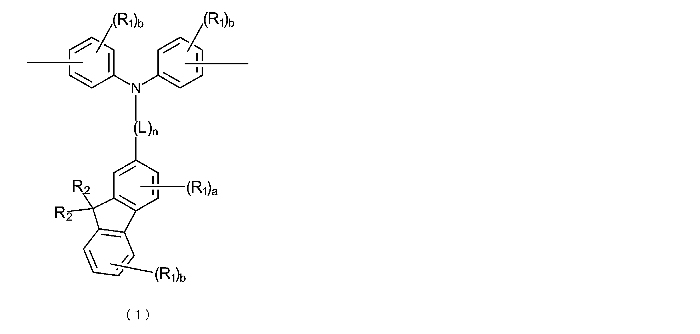
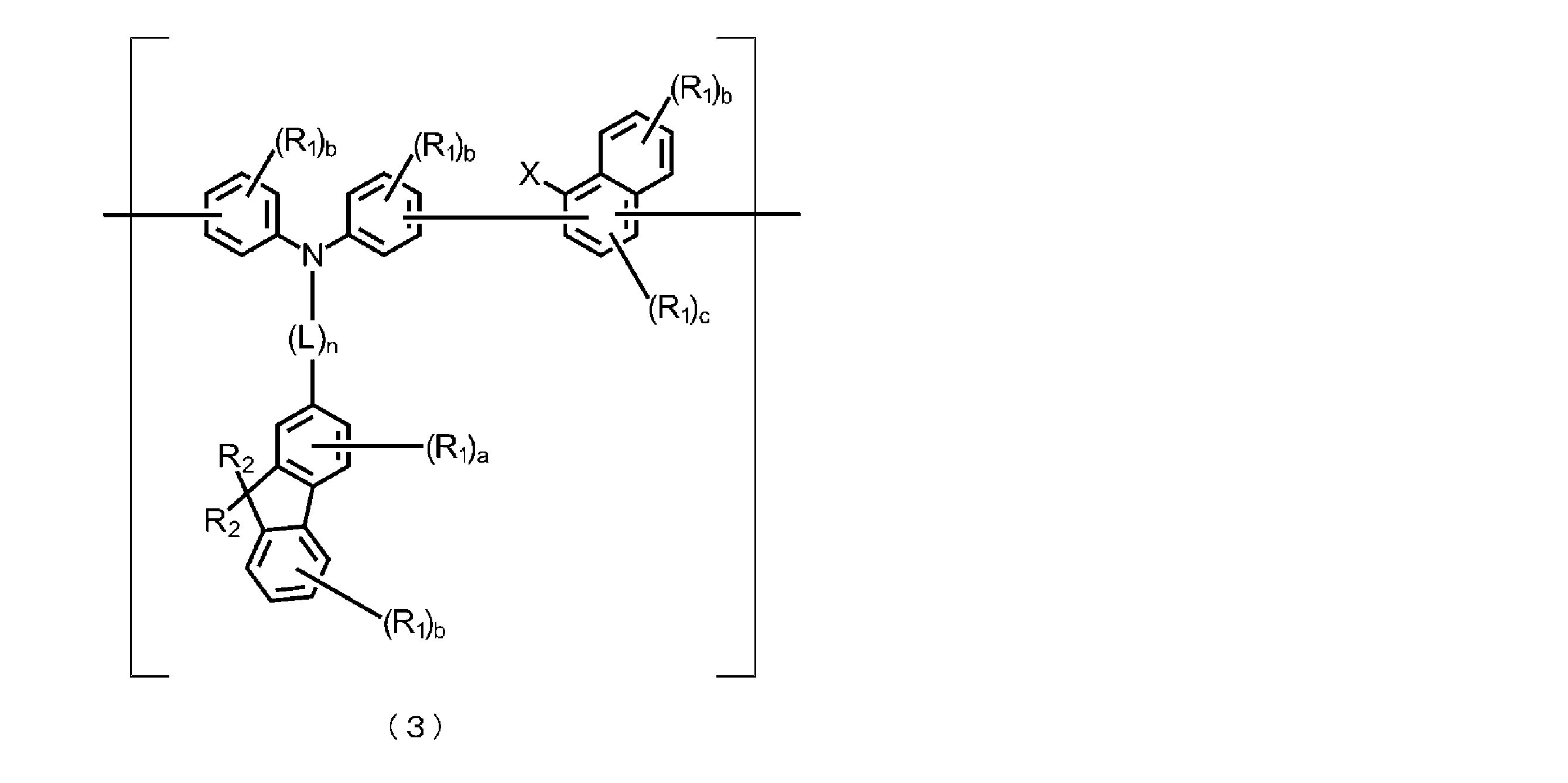
- a repeating structural unit represented by the following general formula (3) which consists of a triarylamine structural unit represented by the following general formula (1) and a connecting structural unit represented by the general formula (2)
- a high molecular weight compound comprising:
- an organic EL device comprising an organic layer formed using the high molecular weight compound.
- the organic layer is preferably a hole-transporting layer, an electron-blocking layer, a hole-injecting layer, or a light-emitting layer.
- a repeating structural unit represented by the following general formula (3) which consists of a triarylamine structural unit represented by the following general formula (1) and a connecting structural unit represented by the following general formula (2). and having a weight average molecular weight of 10,000 or more and less than 1,000,000 in terms of polystyrene.
- each R 1 is independently a hydrogen atom, a deuterium atom, a cyano group, a nitro group, a fluorine atom, a chlorine atom, a bromine atom, an iodine atom, an alkyl group having 1 to 8 carbon atoms, or an alkyloxy group. , a cycloalkyl or cycloalkyloxy group having 5 to 10 carbon atoms, an alkenyl group having 2 to 6 carbon atoms, or an aryloxy group having 6 to 10 carbon atoms.
- Each R 2 independently represents an alkyl group, cycloalkyl group or alkyloxy group having 3 to 40 carbon atoms.
- X represents a hydrogen atom, an amino group, a monovalent aryl group, or a monovalent heteroaryl group.
- L represents a divalent phenylene group or naphthylene group, and n represents an integer of 0-3.
- X is a hydrogen atom, diphenylamino group, phenyl group, naphthyl group, dibenzofuranyl group, dibenzothienyl group, phenanthrenyl group, fluorenyl group, carbazolyl group, indeno
- the dashed line indicates a bond to the adjacent structural unit, and the solid line with a free tip extending from the ring indicates that the tip is a methyl group. showing.
- An organic electroluminescence device comprising an organic layer formed using the high molecular weight compound according to any one of [1] to [7].
- the high molecular weight compound of the present invention comprises a triarylamine structural unit (divalent group) represented by the above-described general formula (1) and a linking structural unit (divalent group) represented by general formula (2).
- the high molecular weight compound of the present invention is (1) good hole injection characteristics; (2) high hole mobility; (3) having a wide gap and excellent electron blocking ability; (4) that the thin film state is stable; It has the characteristic of
- An organic EL device in which an organic layer formed from the high molecular weight compound of the present invention, such as a hole transport layer, an electron blocking layer, a hole injection layer or a light emitting layer, is formed between a pair of electrodes, (1) high luminous efficiency and power efficiency; (2) low practical drive voltage; (3) long life; has the advantage of
- Both the triarylamine structural unit and the linking structural unit possessed by the high molecular weight compound of the present invention are divalent groups represented by the following general formulas (1) and (2), respectively.
- each R 1 is independently a hydrogen atom, a deuterium atom, a cyano group, a nitro group, a fluorine atom, a chlorine atom, a bromine atom, an iodine atom, and having 1 to 1 carbon atoms.
- alkyl group, alkyloxy group, cycloalkyl group, cycloalkyloxy group, alkenyl group and aryloxy group represented by R 1 include the following groups.
- alkyl groups (having 1 to 8 carbon atoms) include methyl, ethyl, n-propyl, isopropyl, n-butyl, isobutyl, tert-butyl, n-pentyl, isopentyl, neopentyl group, n-hexyl group, isohexyl group, neohexyl group, n-heptyl group, isoheptyl group, neoheptyl group, n-octyl group, isooctyl group, neooctyl group and the like.
- alkyloxy groups (having 1 to 8 carbon atoms) include methyloxy, ethyloxy, n-propyloxy, isopropyloxy, n-butyloxy, tert-butyloxy, n-pentyloxy, n -hexyloxy group, n-heptyloxy group, n-octyloxy group and the like.
- cycloalkyl groups (having 5 to 10 carbon atoms) include cyclopentyl, cyclohexyl, 1-adamantyl and 2-adamantyl groups.
- Examples of cycloalkyloxy groups include cyclopentyloxy, cyclohexyloxy, cycloheptyloxy, cyclooctyloxy, 1-adamantyloxy, and 2-adamantyloxy groups.
- Examples of alkenyl groups include vinyl groups, allyl groups, isopropenyl groups and 2-butenyl groups.
- Examples of aryloxy groups include phenyloxy groups and tolyloxy groups.
- R 1 is preferably a deuterium atom. Synthetically, it is most preferred that a, b and c are zero.
- each R 2 independently represents an alkyl group, a cycloalkyl group or an alkyloxy group having 3 to 40 carbon atoms.
- Examples of the alkyl group, cycloalkyl group and alkyloxy group represented by R 2 include the same groups as those represented by R 1 .
- R 2 is preferably an alkyl group having 3 to 40 carbon atoms, most preferably an n-hexyl group or an n-octyl group, in order to increase the solubility. is.
- X represents a hydrogen atom, an amino group, a monovalent aryl group, or a monovalent heteroaryl group.
- Examples of the monovalent aryl group and monovalent heteroaryl group include the following groups.
- aryl groups include phenyl, naphthyl, anthracenyl, phenanthrenyl, fluorenyl, indenyl, pyrenyl, perylenyl, and fluoranthenyl groups.
- heteroaryl groups include pyridyl, pyrimidinyl, triazinyl, furyl, pyrrolyl, thienyl, quinolyl, isoquinolyl, benzofuranyl, benzothienyl, indolyl, carbazolyl, indenocarbazolyl. benzoxazolyl, benzothiazolyl, quinoxalinyl, benzimidazolyl, pyrazolyl, dibenzofuranyl, dibenzothienyl, naphthyridinyl, phenanthrolinyl, acridinyl, and carbolinyl groups.
- amino group, aryl group, and heteroaryl group described above may have a substituent.
- Substituents include deuterium atoms, cyano groups, nitro groups, and the like, halogen atoms such as fluorine, chlorine, bromine, and iodine atoms; Alkyl groups, particularly those having 1 to 8 carbon atoms, such as methyl, ethyl, n-propyl, isopropyl, n-butyl, isobutyl, tert-butyl, n-pentyl, isopentyl, neopentyl, n-hexyl, isohexyl, neohexyl, n-heptyl, isoheptyl, neoheptyl, n-octyl, isooctyl, and neooctyl; alkyloxy groups, especially those having 1 to 8 carbon atoms
- substituents may further have the substituents exemplified above.
- substituents preferably exist independently, but these substituents are separated from each other via a single bond, an optionally substituted methylene group, an oxygen atom or a sulfur atom. may be bonded to each other to form a ring.
- X is a hydrogen atom, a diphenylamino group, a phenyl group, a naphthyl group, a dibenzofuranyl group, a dibenzothienyl group, a phenanthrenyl group, a fluorenyl group, a carbazolyl group, an indenocarbazolyl group, or an acridinyl group. is preferred, and from the viewpoint of synthesis, a hydrogen atom is particularly preferred.
- the above aryl group and heteroaryl group may have a phenyl group as a substituent, and this phenyl group may further have a phenyl group as a substituent.
- the aryl group can be a biphenylyl group, a terphenylyl group, and a triphenylenyl group.
- L represents a divalent phenylene group or naphthylene group
- n represents an integer of 0-3.
- n is preferably 0.
- the above L may have a substituent.
- the substituents are the same as the substituents that X may have, and these substituents may further have a substituent.
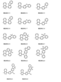
- FIGS. 1 and 2 specific examples of the linking structural unit represented by the general formula (2) are shown in FIGS. 1 and 2 as structural units 1 to 26.
- the dashed line indicates a bond to the adjacent structural unit, and the solid line extending from the ring indicates that the free tip is a methyl group. showing.
- Preferred specific examples of the linking structural unit are shown, but the linking structural unit used in the present invention is not limited to these structural units.
- the high molecular weight of the present invention comprising a repeating unit represented by general formula (3), which consists of the triarylamine structural unit represented by general formula (1) and the linking structural unit represented by general formula (2).
- the compound has excellent properties such as hole injection properties, hole mobility, electron blocking ability, thin film stability, and heat resistance.
- the weight average molecular weight in terms of polystyrene measured by GPC is preferably 10,000 or more and less than 1,000,000, more preferably 10,000 or more and less than 500,000, and further It is preferably in the range of 10,000 or more and less than 200,000.
- the high-molecular-weight compound of the present invention when applied to the formation of an organic layer in an organic EL device by coating, in order to ensure coatability, adhesion to other layers, and durability, other structural units It is preferred to include Such other structural units include, for example, a structural unit for enhancing thermal crosslinkability (thermal crosslinkable structural unit), and a triarylamine structural unit different from the triarylamine structural unit represented by general formula (1). There are structural units.
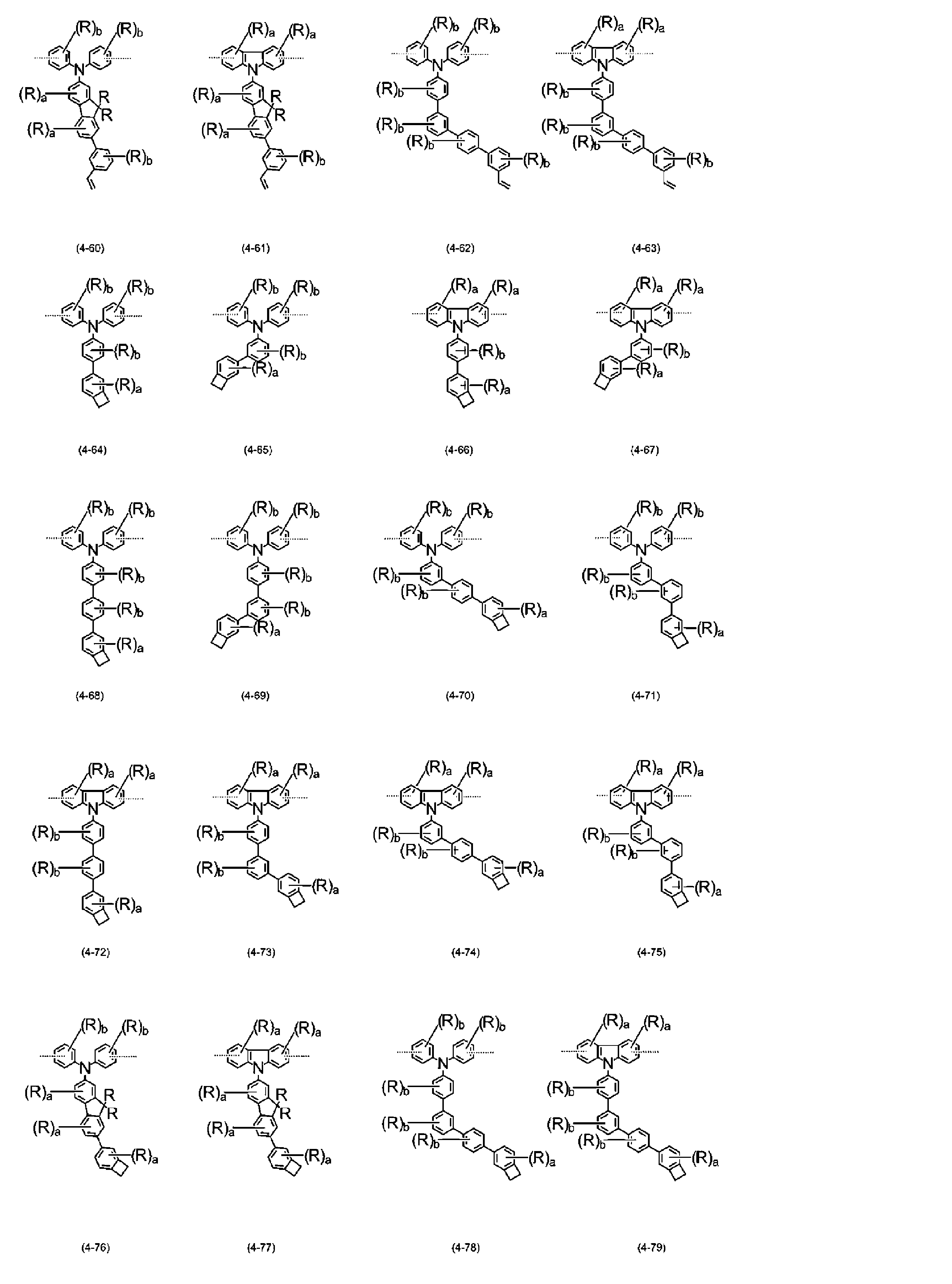
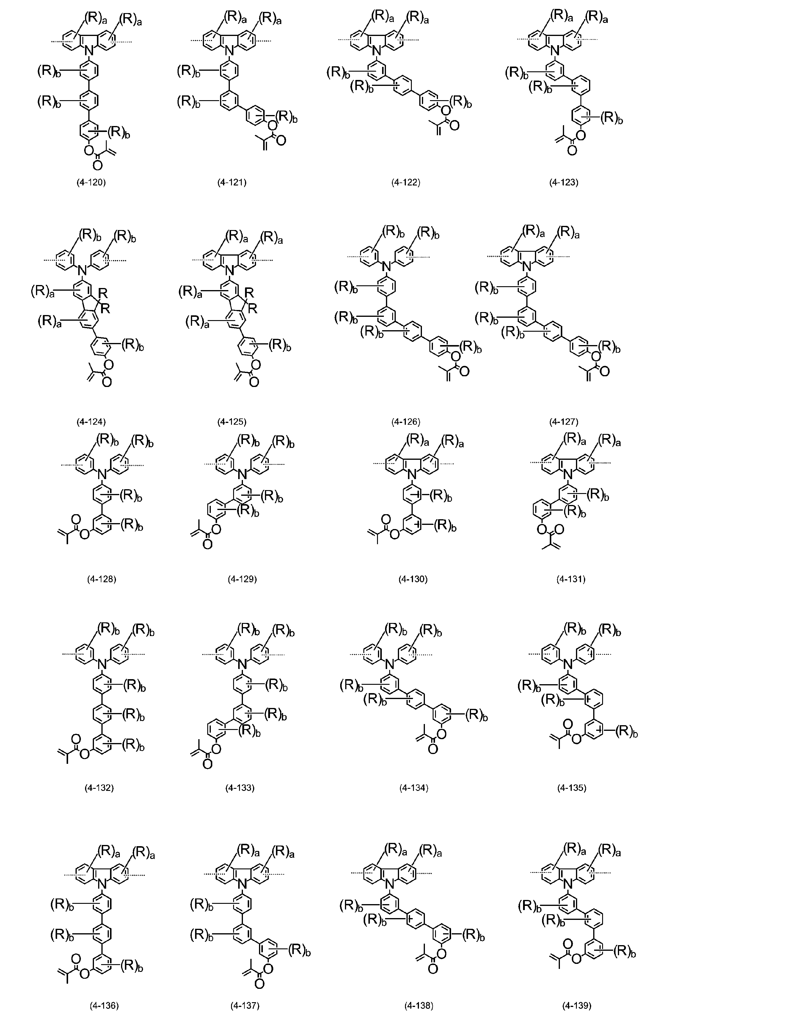
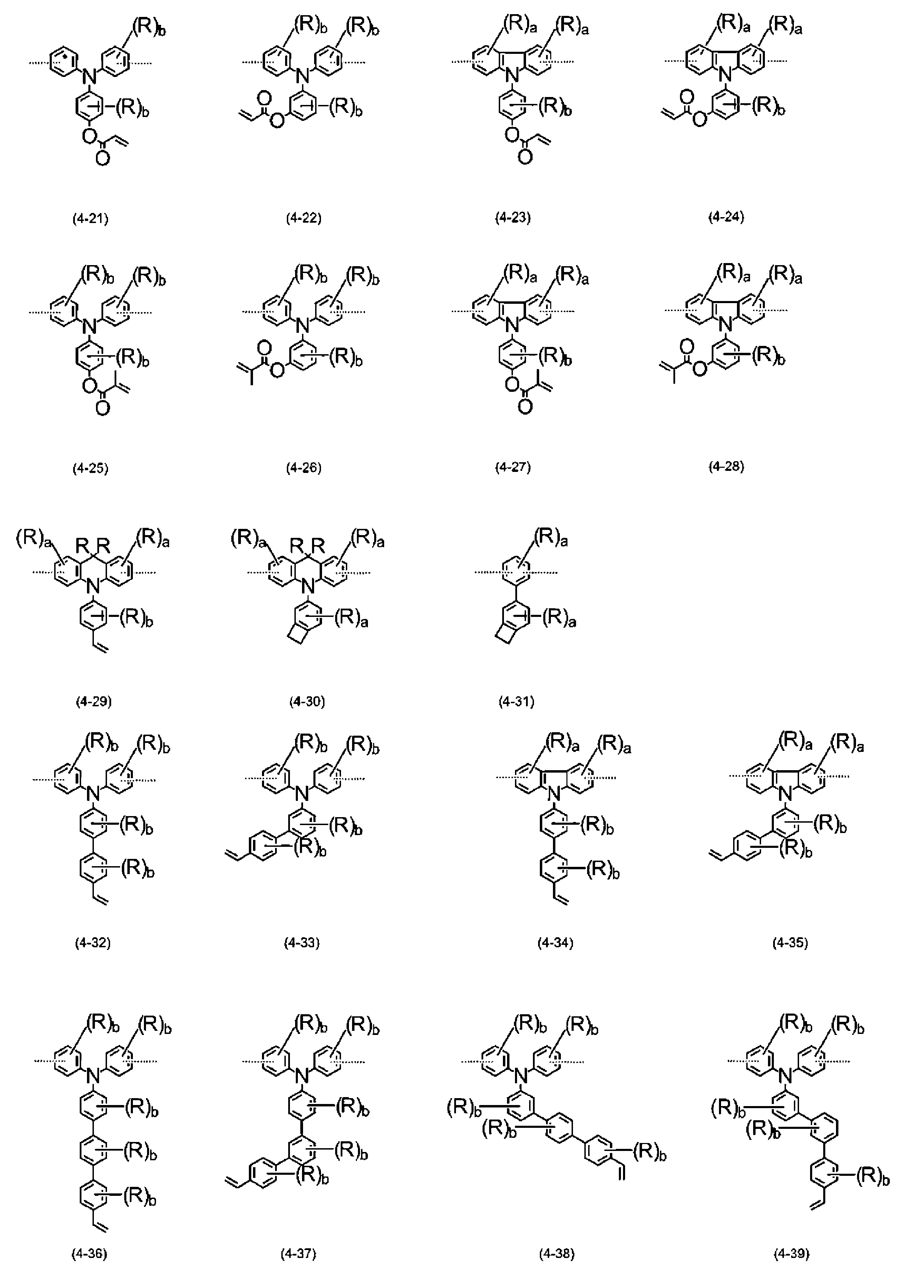
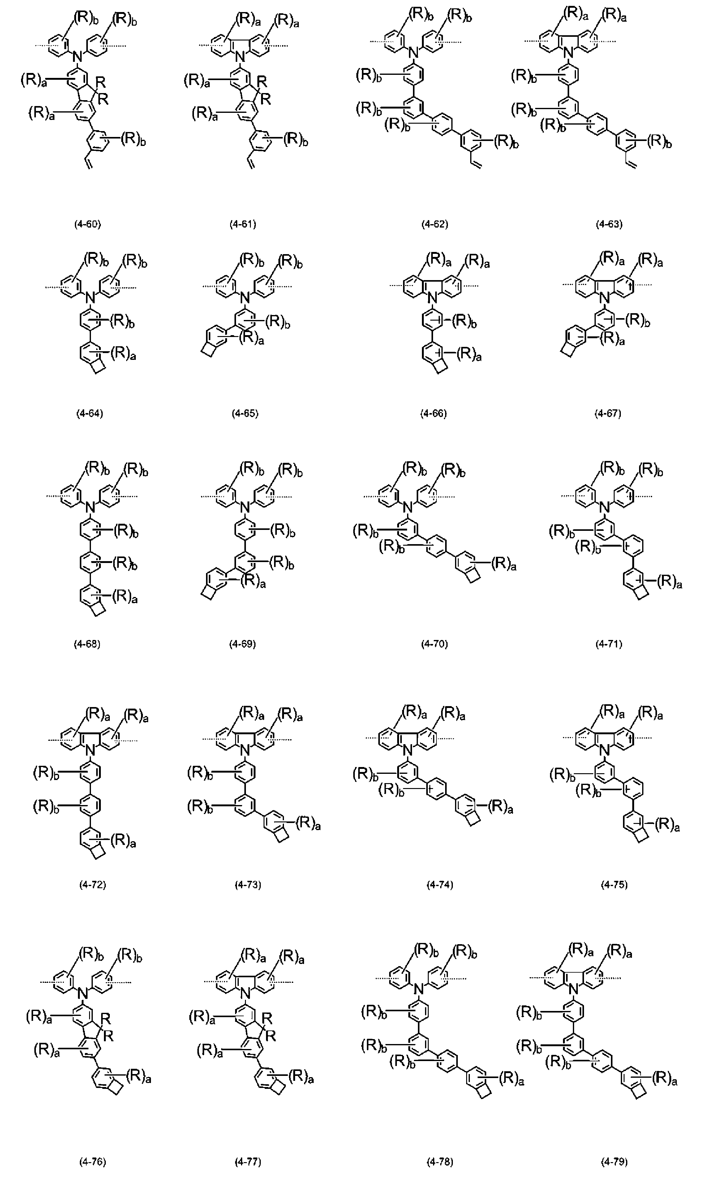
- thermally crosslinkable structural unit examples include the structural units represented by the general formulas (4-1) to (4-143).
- the dashed line indicates a bond to an adjacent structural unit
- R is a hydrogen atom, a deuterium atom, a cyano group, a nitro group, a fluorine atom, a chlorine atom, a bromine atom, an iodine atom, or having 3 to 40, an alkyl group, an alkyloxy group, a cycloalkyl group, a cycloalkyloxy group, an alkenyl group, or an aryloxy group.
- Examples of the alkyl group, alkyloxy group, cycloalkyl group, cycloalkyloxy group, alkenyl group, and aryloxy group represented by R include the same groups as those shown for R 1 .
- Preferred specific examples of the thermally crosslinkable structural unit have been shown, but the thermally crosslinkable structural unit used in the present invention is not limited to these structural units.
- the triarylamine structural unit represented by general formula (1) is "structural unit A”
- the linking structural unit represented by general formula (2) is “structural unit B”
- thermal crosslinking 1 mol of structural unit A is represented by “structural unit C”
- “structural unit D” is a triarylamine structural unit different from the triarylamine structural unit represented by general formula (1).
- % or more particularly 20 mol % or more
- the structural unit B is 1 mol % or more, particularly 30 to 70 mol %.
- it preferably contains structural unit C in an amount of 1 mol% or more, particularly 5 to 20 mol%.
- a copolymer is most suitable for forming an organic layer of an organic EL device.
- the high-molecular-weight compounds of the present invention are synthesized by forming carbon-carbon bonds or carbon-nitrogen bonds, respectively, and linking structural units by Suzuki polymerization reaction or HARTWIG-BUCHWALD polymerization reaction. Specifically, a unit compound having each structural unit is prepared, the unit compound is appropriately boric acid esterified or halogenated, and polycondensation reaction is performed using an appropriate catalyst to obtain the high molecular weight compound of the present invention. Can be synthesized.
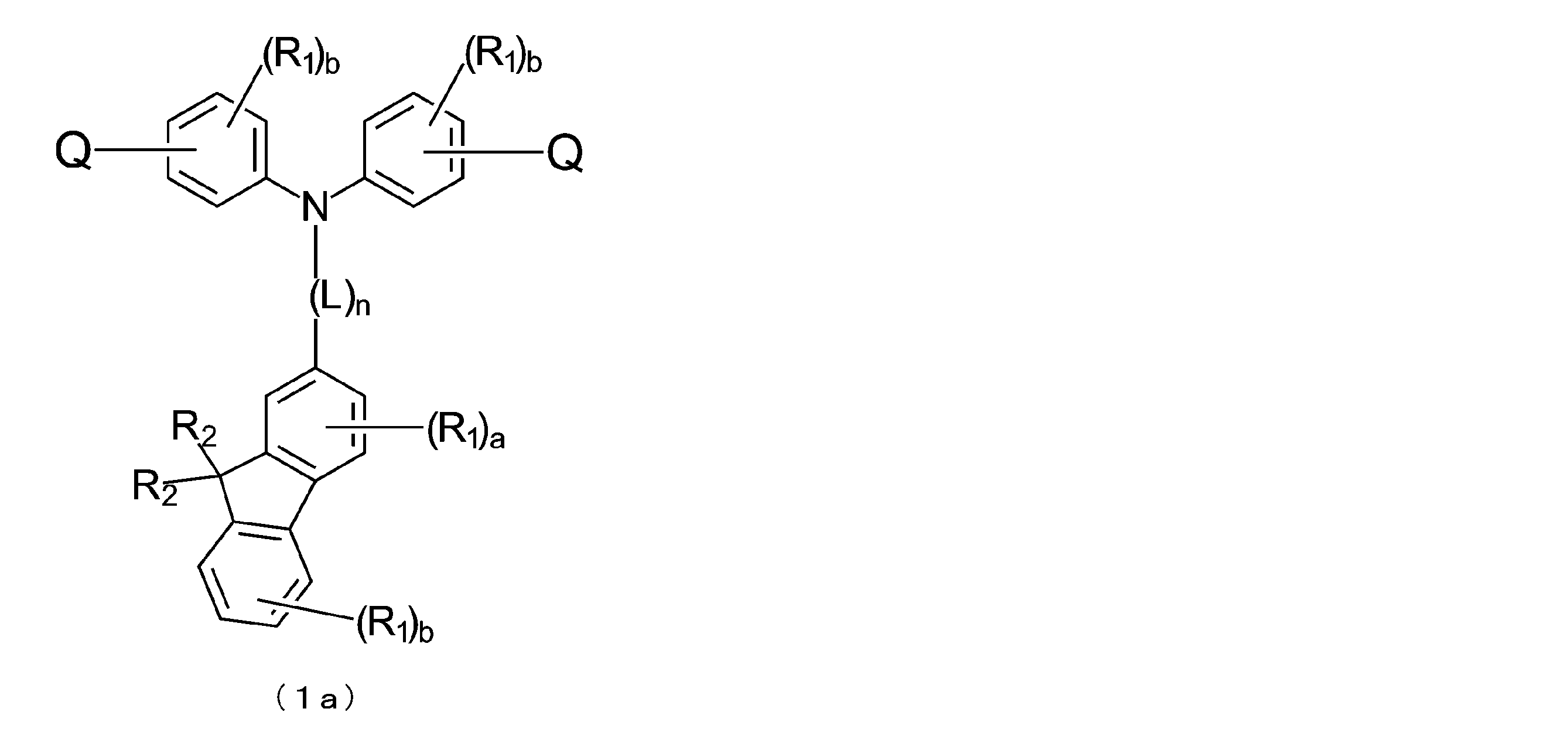
- a triarylamine derivative represented by the following general formula (1a) can be used as a compound for introducing the triarylamine structural unit represented by the general formula (1).
- Q is a hydrogen atom or a halogen atom (particularly preferably Br), and R 1 , R 2 and L are all the same as defined in general formula (1) above. be.
- the compound in which Q is a hydrogen atom is a unit compound for introducing the triarylamine structural unit represented by the general formula (1), and the compound in which Q is a halogen atom. is the halide used to synthesize the polymer.
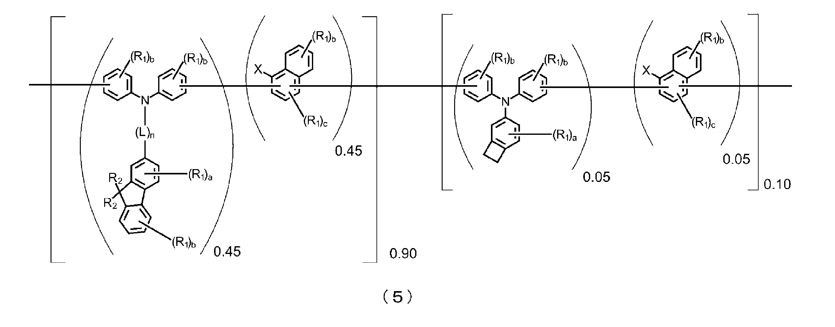
- thermally crosslinkable structural unit C (general thermally crosslinkable structural unit A copolymer containing 5 mol % of formula (4-5)) is represented by the following general formula (5).
- the intermediate for introducing the structural unit A and the structural unit C is a borate ester
- the intermediate for introducing the structural unit B is a halide
- the structural The intermediate for introducing the unit A and the structural unit C must be a halide
- the intermediate for introducing the structural unit B must be a boric acid ester. That is, the molar ratios of halide and borate esters must be equal.
- the above-described high molecular weight compound of the present invention is dissolved in an aromatic organic solvent such as benzene, toluene, xylene and anisole to prepare a coating liquid, which is coated on a predetermined substrate and dried by heating.
- an aromatic organic solvent such as benzene, toluene, xylene and anisole.
- the high molecular weight compound can be used as a constituent material of the hole injection layer and/or the hole transport layer of the organic EL device.
- a hole injection layer and a hole transport layer formed of such a high molecular weight compound have higher hole injection properties, higher hole mobility, and electron blocking properties than those formed of conventional materials. is high, excitons generated in the light-emitting layer can be confined, the probability of recombination of holes and electrons can be improved, high luminous efficiency can be obtained, and the driving voltage can be lowered, and the organic EL The advantage of improved device durability can be realized.
- the high molecular weight compound of the present invention having the above-described electrical properties has a wider gap than conventional materials and is effective in confining excitons, so it is naturally suitable for use in electron blocking layers and light-emitting layers. can do.
- An organic EL device having an organic layer formed using the high-molecular-weight compound of the present invention has a structure shown in FIG. 3, for example. That is, a transparent anode 2, a hole injection layer 3, a hole transport layer 4, a light emitting layer 5, an electron transport layer 6 and a cathode 7 are formed on a glass substrate 1 (a transparent substrate such as a transparent resin substrate may be used). is provided.
- the organic EL device to which the high molecular weight compound of the present invention is applied is not limited to the layer structure described above, and a hole blocking layer can be provided between the light emitting layer 5 and the electron transport layer 6, and , as in the structure shown in FIG. Furthermore, an electron injection layer can be provided between the cathode and the electron transport layer. Additionally, some layers may be omitted. For example, a simple layer structure in which an anode, a hole-transporting layer, a light-emitting layer, an electron-transporting layer and a cathode are provided on a substrate may be employed. It is also possible to have a two-layer structure in which layers having the same function are superimposed.
- the high-molecular-weight compound of the present invention utilizes its properties such as hole-injecting properties and hole-transporting properties to provide an organic layer (for example, a hole-injecting layer, a hole-transporting layer) provided between the anode and the cathode. , light emitting layer and electron blocking layer).
- organic layer for example, a hole-injecting layer, a hole-transporting layer
- light emitting layer and electron blocking layer for example, a light emitting layer and electron blocking layer.
- the transparent anode may be formed of an electrode material known per se, and an electrode material having a large work function such as ITO and gold is vapor-deposited on a substrate (a transparent substrate such as a glass substrate). It is formed by
- the hole injection layer provided on the transparent anode can be formed using a coating solution prepared by dissolving the high molecular weight compound of the present invention in an aromatic organic solvent such as toluene, xylene and anisole. can.
- the hole injection layer can be formed by coating this coating liquid on the transparent anode by spin coating, inkjet, or the like.
- the hole injection layer is formed of a conventionally known material such as the following, without using the high molecular weight compound of the present invention. It can also be formed using a material.
- PEDOT poly(3,4-ethylenedioxythiophene)
- PSS poly(styrene sulfonate)
- a layer (thin film) using such a material can be formed by a coating method such as vapor deposition, spin coating, and inkjet. The same applies to other layers, and the film is formed by vapor deposition or coating depending on the type of film-forming material.
- the hole transport layer provided on the hole injection layer can also be formed using the high molecular weight compound of the present invention by a coating method such as spin coating or inkjet. can.
- a hole transport layer can be formed using a conventionally known hole transport material.
- Typical examples of such hole transport materials are as follows.
- benzidine derivatives such as N,N'-diphenyl-N,N'-di(m-tolyl)benzidine (hereinafter abbreviated as TPD); N,N'-diphenyl-N,N'-di( ⁇ -naphthyl)benzidine (hereinafter abbreviated as NPD); N,N,N',N'-tetrabiphenylylbenzidine;
- Amine derivatives such as 1,1-bis[4-(di-4-tolylamino)phenyl]cyclohexane (hereinafter abbreviated as TAPC); various triphenylamine trimers and tetramers;
- a coating-type polymer material that is also used as a hole injection layer.
- the compounds for the hole transport layer described above including the high-molecular-weight compound of the present invention, may be formed individually, or two or more of them may be mixed to form a film. Also, a multilayer film in which a plurality of layers are formed using one or more of the above compounds and such layers are laminated can be used as the hole transport layer.
- a layer that serves both as a hole-injecting layer and a hole-transporting layer can be used.
- the transport layer can be formed by a coating method using a polymeric material such as PEDOT.
- the hole-transporting layer (the same applies to the hole-injecting layer), tris(4-bromophenyl)ammoniumylhexachloroantimonate or a radialene derivative (see, for example, WO2014/009310) is used as a material normally used for the layer. etc. can be used by P-doping.
- the hole transport layer (and the hole injection layer) can be formed using a polymer compound having a TPD basic skeleton.
- an electron-blocking layer (which can be provided between the hole-transporting layer 11 and the light-emitting layer 13, as shown in FIG. 4) is also coated using the high-molecular-weight compound of the present invention by a coating method such as spin coating and inkjet. can be formed by
- an electron-blocking compound having an electron-blocking action such as a carbazole derivative or a triphenylsilyl group
- An electron blocking layer can also be formed using a compound having a triarylamine structure.
- carbazole derivatives and compounds having a triarylamine structure are as follows.
- carbazole derivatives such as 4,4′,4′′-tri(N-carbazolyl)triphenylamine (hereinafter abbreviated as TCTA); 9,9-bis[4-(carbazol-9-yl)phenyl]fluorene; 1,3-bis(carbazol-9-yl)benzene (hereinafter abbreviated as mCP); 2,2-bis(4-carbazol-9-ylphenyl)adamantane (hereinafter abbreviated as Ad-Cz); Compounds having a triarylamine structure, such as 9-[4-(carbazol-9-yl)phenyl]-9-[4-(triphenylsilyl)phenyl]-9H-fluorene.
- TCTA 4,4′,4′′-tri(N-carbazolyl)triphenylamine
- mCP 1,3-bis(carbazol-9-yl)benzene
- Ad-Cz 2,2-bis(4-carbazol-9
- the electron blocking layer including the high molecular weight compound of the present invention, may be formed independently, but it is also possible to form a film by mixing two or more kinds. Also, a multilayer film in which a plurality of layers are formed using one or more of the above compounds and such layers are laminated can be used as the electron blocking layer.
- the light-emitting layer comprises metal complexes of quinolinol derivatives such as Alq3 ; various metal complexes such as zinc, beryllium and aluminum; It can be formed using a light-emitting material such as an anthracene derivative; a bisstyrylbenzene derivative; a pyrene derivative; an oxazole derivative;
- the light-emitting layer can be composed of a host material and a dopant material.
- a host material in addition to the light-emitting materials described above, thiazole derivatives, benzimidazole derivatives, polydialkylfluorene derivatives, and the like can be used, and furthermore, the high molecular weight compounds of the present invention described above can also be used.
- Quinacridone, coumarin, rubrene, perylene, and derivatives thereof; benzopyran derivatives; rhodamine derivatives; aminostyryl derivatives and the like can be used as dopant materials.
- Such a light-emitting layer can also have a single-layer structure using one or more of each light-emitting material, or can have a multi-layer structure in which a plurality of layers are laminated.
- the light-emitting layer can also be formed using a phosphorescent light-emitting material as the light-emitting material.
- a phosphorescent light-emitting material phosphorescent emitters of metal complexes such as iridium and platinum can be used.
- green phosphorescent emitters such as Ir(ppy) 3
- blue phosphorescent emitters such as FIrpic and FIr6
- red phosphorescent emitters such as Btp2Ir (acac) can be used.
- These phosphorescent materials are used by doping a hole-injecting/transporting host material or an electron-transporting host material.
- doping of the host material with the phosphorescent light-emitting material is preferably carried out by co-evaporation in the range of 1 to 30% by weight with respect to the entire light-emitting layer.
- the high molecular weight compound of the present invention carry a fluorescent emitter, a phosphorescent emitter, or a material that emits delayed fluorescence, which is called a dopant, to form a light-emitting layer, the driving voltage is lowered and the luminous efficiency is improved. It is possible to realize an organic EL element with
- the high molecular weight compound of the present invention can be used as a hole-injecting/transporting host material.
- CBP 4,4'-di(N-carbazolyl)biphenyl
- carbazole derivatives such as TCTA and mCP, and the like can also be used.
- p-bis(triphenylsilyl)benzene (hereinafter abbreviated as UGH2) is used as the electron-transporting host material.
- UGH2 p-bis(triphenylsilyl)benzene
- TPBI 2,2′,2′′-(1,3,5-phenylene)-tris(1-phenyl-1H-benzimidazole)
- a hole-blocking layer (not shown in the figure) provided between the light-emitting layer and the electron-transporting layer includes It can be formed using a compound having a known hole-blocking action. Examples of known compounds having such a hole-blocking action include the following.
- phenanthroline derivatives such as bathocuproine (hereinafter abbreviated as BCP); metal complexes of quinolinol derivatives such as aluminum (III) bis(2-methyl-8-quinolinate)-4-phenylphenolate (hereinafter abbreviated as BAlq); various rare earth complexes; triazole derivatives; triazine derivatives; Oxadiazole derivatives.
- BCP bathocuproine
- BAlq metal complexes of quinolinol derivatives
- BAlq aluminum (III) bis(2-methyl-8-quinolinate)-4-phenylphenolate
- various rare earth complexes such as triazole derivatives; triazine derivatives; Oxadiazole derivatives.
- These materials can also be used to form the electron-transporting layer described below, and can also be used as both a hole-blocking layer and an electron-transporting layer.
- Such a hole-blocking layer can also have a single-layer or multi-layer laminated structure, and each layer is formed using one or more of the compounds having the hole-blocking action described above.
- the electron-transporting layer is composed of an electron-transporting compound known per se, such as a quinolinol derivative such as Alq 3 and BAlq. It can be formed using metal complexes, various metal complexes, pyridine derivatives, pyrimidine derivatives, triazole derivatives, triazine derivatives, oxadiazole derivatives, thiadiazole derivatives, carbodiimide derivatives, quinoxaline derivatives, phenanthroline derivatives, silole derivatives, benzimidazole derivatives, and the like. can.
- an electron-transporting compound known per se such as a quinolinol derivative such as Alq 3 and BAlq. It can be formed using metal complexes, various metal complexes, pyridine derivatives, pyrimidine derivatives, triazole derivatives, triazine derivatives, oxadiazole derivatives, thiadiazole derivatives, carbodiimide derivatives, quinoxaline derivatives, phenanthroline derivative
- This electron-transporting layer can also have a single-layer or multi-layer laminated structure, and each layer is formed using one or more of the electron-transporting compounds described above.
- the electron injection layer (not shown in the figure) provided as necessary is also known per se, such as , alkali metal salts such as lithium fluoride and cesium fluoride, alkaline earth metal salts such as magnesium fluoride, metal oxides such as aluminum oxide, and organometallic complexes such as lithium quinoline. .
- an electrode material having a low work function such as aluminum, and a magnesium-silver alloy, a magnesium-indium alloy, or an aluminum-magnesium alloy can be used.
- An alloy with a lower work function, such as, is used as an electrode material.
- the high molecular weight compound of the present invention is used to form at least one layer of a hole injection layer, a hole transport layer, a light emitting layer, and an electron blocking layer, thereby improving luminous efficiency and power consumption.
- An organic EL device having high efficiency, low practical driving voltage, low light emission start voltage, and extremely excellent durability can be obtained.
- this organic EL element while having high luminous efficiency, the driving voltage is lowered, the current resistance is improved, and the maximum luminous luminance is improved.
- the structural unit represented by the general formula (1) of the high molecular weight compound of the present invention is "structural unit A”
- the connecting structural unit represented by general formula (2) is “structural unit B ”
- Example 1 Synthesis of High Molecular Weight Compound A; The following ingredients were added to a reaction vessel purged with nitrogen, and nitrogen gas was bubbled through for 30 minutes.
- Intermediate 1 5.6 g
- Intermediate 2 0.4g
- Intermediate 3 2.2 g
- Tripotassium phosphate 6.9 g
- Toluene 9ml
- Water 5ml 1,4-dioxane: 27 ml
- 1.4 mg of palladium(II) acetate and 11.5 mg of tri-o-tolylphosphine were added, heated, and stirred at 87° C. for 14 hours.
- the average molecular weight and dispersity of high molecular weight compound A measured by GPC were as follows. Number average molecular weight Mn (converted to polystyrene): 60,000 Weight average molecular weight Mw (converted to polystyrene): 108,000 Dispersity (Mw/Mn): 1.8
- this high molecular weight compound A contained 45 mol% of structural unit A, 50 mol% of structural unit B, and 5 mol% of structural unit C.
- Example 2 Synthesis of high molecular weight compound B; The following ingredients were added to a reaction vessel purged with nitrogen, and nitrogen gas was bubbled through for 30 minutes.
- Intermediate 1 5.4 g
- Intermediate 3 2.2 g
- Intermediate 4 0.5g Tripotassium phosphate: 7.4 g
- 1.5 mg of palladium(II) acetate and 14.4 mg of tri-o-methoxyphenylphosphine were added, heated, and stirred at 87° C. for 10 hours.
- the crude polymer was dissolved in toluene, silica gel was added for adsorption purification, and the silica gel was removed by filtration.
- the obtained filtrate was concentrated under reduced pressure, 100 ml of toluene was added to the dried solid to dissolve it, and the solution was added dropwise to 300 ml of n-hexane, and the resulting precipitate was collected by filtration. 100 ml of toluene was added to the obtained precipitate to dissolve it, and the solution was added dropwise to 200 ml of n-hexane, and the obtained precipitate was collected by filtration. This operation was repeated one more time and dried to obtain 3.2 g of high molecular weight compound B (yield: 67%).
- the average molecular weight and dispersity of high molecular weight compound B measured by GPC were as follows. Number average molecular weight Mn (converted to polystyrene): 73,000 Weight average molecular weight Mw (converted to polystyrene): 139,000 Dispersity (Mw/Mn): 1.9
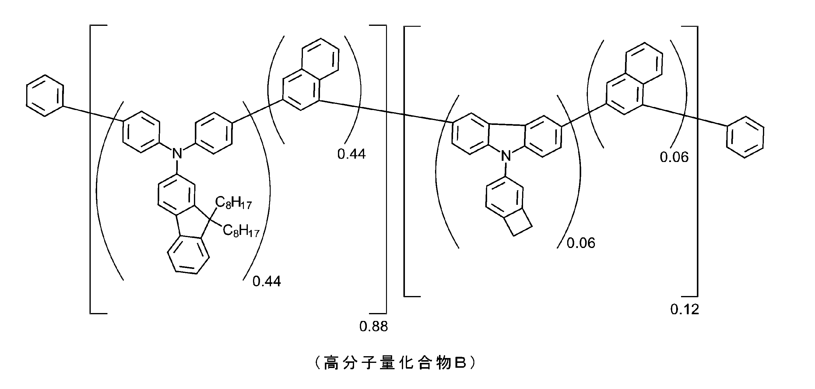
- this high molecular weight compound B contained 44 mol% of structural unit A, 50 mol% of structural unit B, and 6 mol% of structural unit C.
- Example 3 Using the high molecular weight compounds A and B synthesized in Examples 1 and 2, a coating film having a thickness of 80 nm was prepared on an ITO substrate, and an ionization potential measuring device (manufactured by Sumitomo Heavy Industries, Ltd., PYS- 202 type) to measure the work function. The results were as follows. High molecular weight compound A: 5.63 eV High molecular weight compound B: 5.61 eV
- the high molecular weight compound A of the present invention exhibits a favorable energy level compared to the work function of 5.4 eV of general hole-transporting materials such as NPD and TPD, and exhibits good hole-transporting ability. I know you have.
- An organic EL device having a layered structure shown in FIG. 3 was produced by the following method. Specifically, after washing the glass substrate 1 with an ITO film having a film thickness of 50 nm with an organic solvent, the ITO surface was washed with UV/ozone treatment. PEDOT/PSS (manufactured by Ossila) was spin-coated to a thickness of 50 nm so as to cover the transparent anode 2 (ITO) provided on the glass substrate 1, and dried on a hot plate at 200° C. for 10 minutes. Then, a hole injection layer 3 was formed.
- PEDOT/PSS manufactured by Ossila
- a coating liquid was prepared by dissolving 0.6 wt % of the high molecular weight compound A obtained in Example 1 in toluene.
- the substrate on which the hole injection layer 3 is formed as described above is transferred into a glove box replaced with dry nitrogen, dried on a hot plate at 230° C. for 10 minutes, and then placed on the hole injection layer 3.
- a coating layer having a thickness of 25 nm was formed by spin coating using the above coating liquid, and dried on a hot plate at 220° C. for 30 minutes to form a hole transport layer 4 .
- the substrate on which the hole transport layer 4 was formed as described above was mounted in a vacuum deposition machine, and the pressure was reduced to 0.001 Pa or less.
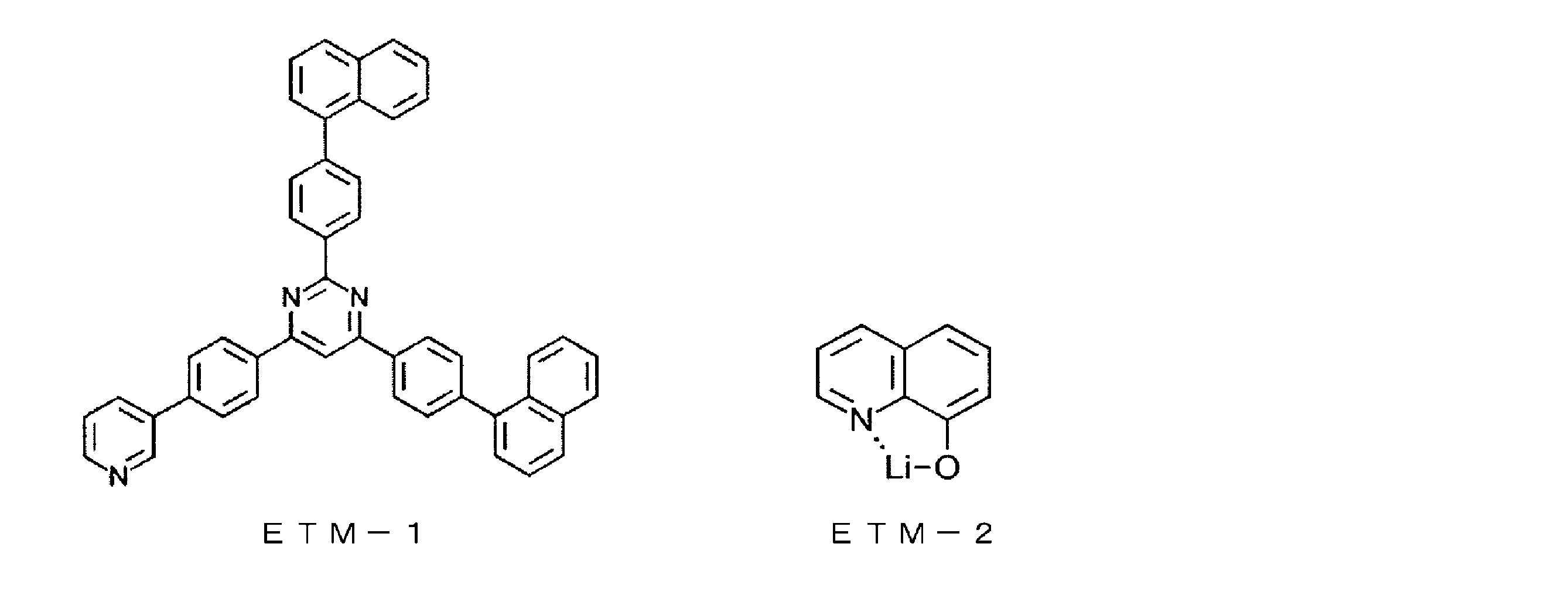
- ETM-1 and ETM-2 compounds of the following structural formulas, were prepared as electron transport materials.
- an electron-transporting layer 6 having a thickness of 20 nm was formed by binary vapor deposition using the electron-transporting materials ETM-1 and ETM-2.
- a cathode 7 was formed by vapor-depositing aluminum to a film thickness of 100 nm.
- the glass substrate on which the transparent anode 2, the hole injection layer 3, the hole transport layer 4, the light emitting layer 5, the electron transport layer 6 and the cathode 7 are formed is placed in a glove box filled with dry nitrogen. It was moved, and another glass substrate for sealing was bonded together using a UV curable resin to form an organic EL element.
- the characteristics of the produced organic EL device were measured at room temperature in the air. Further, the luminescence characteristics were measured when a DC voltage was applied to the produced organic EL device. The measurement results are shown in Table 1.
- Example 4 except that a coating solution prepared by dissolving 0.6 wt % of the following TFB (hole-transporting polymer) in toluene instead of the high-molecular-weight compound A was used to form the hole-transporting layer 4.
- An organic EL device was produced in the same manner as above.
- TFB hole-transporting polymer
- PFA hole-transporting polymer
- Various characteristics of the organic EL device of Comparative Example 1 were evaluated in the same manner as in Example 4, and the results are shown in Table 1.
- the voltage, luminance, luminous efficiency and power efficiency are obtained when a current with a current density of 10 mA/cm 2 is applied.
- life of the element was measured by constant current driving with a light emission luminance of 700 cd/m 2 at the start of light emission (initial luminance) of 560 cd/m 2 (80% of the initial luminance of 100%). Equivalent: measured as the time to decay to 80% decay).
- the luminous efficiency of the organic EL device of Comparative Example 1 was 5.52 cd/A when a current with a current density of 10 mA/cm 2 was applied, while the organic EL device of Example 4 was 7.52 cd/A. It was highly efficient at .83 cd/A.
- the device life (80% attenuation) was 248 hours for the organic EL device of Example 4, which is longer than the 6 hours for the organic EL device of Comparative Example 1.
- An organic EL device having a layer structure shown in FIG. 4 was produced by the following method. Specifically, after washing the glass substrate 8 with an ITO film having a thickness of 50 nm with an organic solvent, the ITO surface was washed with UV/ozone treatment. PEDOT/PSS (manufactured by Ossila) was spin-coated to a thickness of 50 nm so as to cover the transparent anode 9 (ITO) provided on the glass substrate 8, and dried on a hot plate at 200° C. for 10 minutes. Then, a hole injection layer 10 was formed.
- PEDOT/PSS manufactured by Ossila
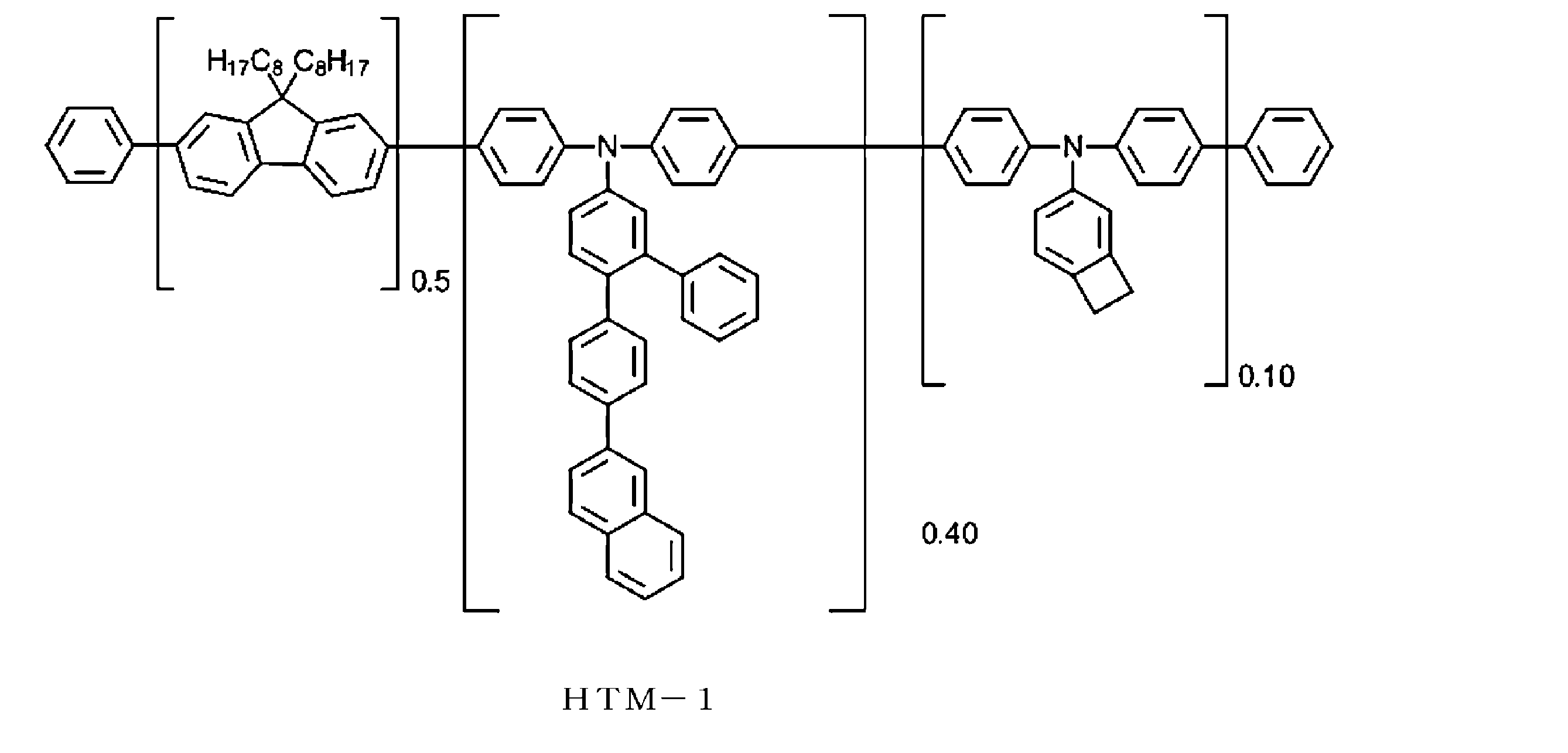
- a coating liquid was prepared by dissolving 0.4 wt% of a high molecular weight compound HTM-1 having the following structural formula in toluene.
- the substrate on which the hole injection layer 10 is formed as described above is transferred into a glove box replaced with dry nitrogen, and dried on a hot plate at 230° C. for 10 minutes.
- a coating layer having a thickness of 15 nm was formed by spin coating using the above coating solution, and dried on a hot plate at 220° C. for 30 minutes to form a hole transport layer 11 .
- a coating liquid was prepared by dissolving 0.4 wt % of the high molecular weight compound A obtained in Example 1 in toluene.
- a coating layer having a thickness of 15 nm is formed on the hole transport layer 11 by spin coating using the above coating liquid, and dried on a hot plate at 220° C. for 30 minutes to form an electron blocking layer 12 . did.
- the substrate on which the electron blocking layer 12 was formed as described above was mounted in a vacuum deposition machine and the pressure was reduced to 0.001 Pa or less.
- an electron transporting layer 14 having a thickness of 20 nm was formed by binary vapor deposition using the electron transporting materials ETM-1 and ETM-2.
- a cathode 15 was formed by vapor-depositing aluminum to a film thickness of 100 nm.
- the glass substrate on which the transparent anode 9, the hole injection layer 10, the hole transport layer 11, the electron blocking layer 12, the light emitting layer 13, the electron transport layer 14 and the cathode 15 are formed is replaced with dry nitrogen.
- another glass substrate for sealing was attached using a UV curable resin to form an organic EL element.
- the characteristics of the produced organic EL device were measured at room temperature in the atmosphere. Further, the luminescence characteristics were measured when a DC voltage was applied to the produced organic EL device. The measurement results are shown in Table 2.
- Example 5 except that the electron blocking layer 12 was formed using a coating liquid prepared by dissolving 0.4 wt % of the high molecular weight compound B obtained in Example 2 in toluene instead of the high molecular weight compound A.
- An organic EL device was produced in exactly the same manner. Various characteristics of the produced organic EL device were evaluated in the same manner as in Example 5, and the results are shown in Table 2.
- An organic EL device having a layer structure shown in FIG. 4 was produced by the following method. Specifically, after washing the glass substrate 8 with an ITO film having a thickness of 50 nm with an organic solvent, the ITO surface was washed with UV/ozone treatment. PEDOT/PSS (manufactured by Ossila) was spin-coated to a thickness of 50 nm so as to cover the transparent anode 9 (ITO) provided on the glass substrate 8, and dried on a hot plate at 200° C. for 10 minutes. Then, a hole injection layer 10 was formed.
- PEDOT/PSS manufactured by Ossila
- a coating liquid was prepared by dissolving 0.6 wt% of the high molecular weight compound HTM-1 in toluene.
- the substrate on which the hole injection layer 10 is formed as described above is transferred into a glove box filled with dry nitrogen, and the above coating solution is applied onto the hole injection layer 3 by a spin coating method.
- a coating layer having a thickness of 25 nm was formed and dried on a hot plate at 220° C. for 30 minutes to form hole transport layer 11 .
- the substrate on which the hole transport layer 11 was formed as described above was mounted in a vacuum deposition machine, and the pressure was reduced to 0.001 Pa or less.
- a cathode 15 was formed by vapor-depositing aluminum to a film thickness of 100 nm.
- the glass substrate on which the transparent anode 9, the hole injection layer 10, the hole transport layer 11, the light emitting layer 13, the electron transport layer 14 and the cathode 15 are formed is placed in a glove box substituted with dry nitrogen. It was moved, and another glass substrate for sealing was bonded together using a UV curable resin to form an organic EL element.
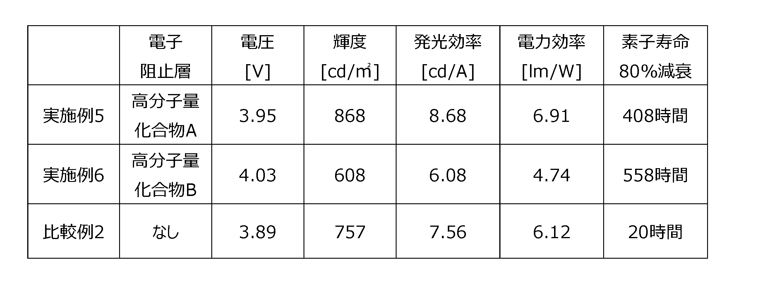
- the characteristics of the produced organic EL device were measured at room temperature in the atmosphere. Further, the luminescence characteristics were measured when a DC voltage was applied to the produced organic EL device. The measurement results are shown in Table 2.
- the voltage, luminance, luminous efficiency and power efficiency are obtained when a current with a current density of 10 mA/cm 2 is applied.
- life of the element was measured by constant current driving with a light emission luminance of 700 cd/m 2 at the start of light emission (initial luminance) of 560 cd/m 2 (80% of the initial luminance of 100%). Equivalent: measured as the time to decay to 80% decay).
- the luminous efficiency of the organic EL device of Comparative Example 2 was 7.56 cd/A when a current with a current density of 10 mA/cm 2 was applied, while the organic EL device of Example 5 was 8.56 cd/A. It was highly efficient at .68 cd/A.
- the device life (80% decay) was 20 hours for the organic EL device of Comparative Example 2, 408 hours for the organic EL device of Example 5, and 558 hours for the organic EL device of Example 6. It had a long life.
- the organic EL element having the organic layer formed using the high molecular weight compound of the present invention can realize an organic EL element with high luminous efficiency and long life as compared with conventional organic EL elements. I found out.
- the high-molecular-weight compound of the present invention has high hole-transporting ability, excellent electron-blocking ability, and good thermal crosslinkability, so it is excellent as a compound for coating-type organic EL devices.
- a coating-type organic EL device using the high molecular weight compound of the present invention high luminous efficiency and power efficiency can be obtained, and durability can be improved. As a result, it has become possible to develop it into a wide range of applications such as home appliances and lighting, for example.
Landscapes
- Physics & Mathematics (AREA)
- Optics & Photonics (AREA)
- Chemical & Material Sciences (AREA)
- Health & Medical Sciences (AREA)
- Chemical Kinetics & Catalysis (AREA)
- Medicinal Chemistry (AREA)
- Polymers & Plastics (AREA)
- Organic Chemistry (AREA)
- Engineering & Computer Science (AREA)
- Materials Engineering (AREA)
- Electroluminescent Light Sources (AREA)
Abstract
Description
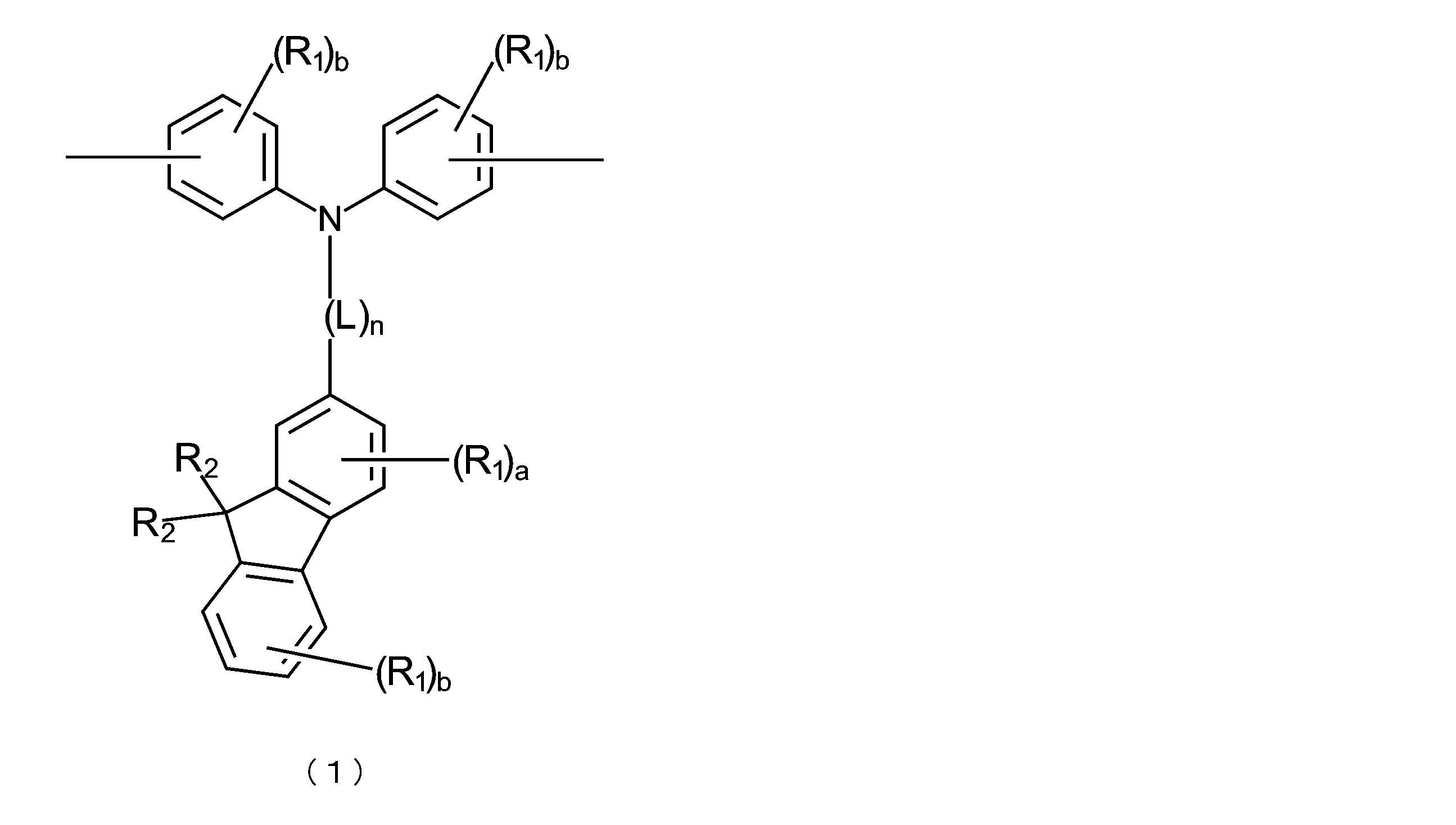


R2は、それぞれ独立に、炭素数が3~40である、アルキル基、シクロアルキル基、またはアルキルオキシ基を示す。
Xは、水素原子、アミノ基、1価のアリール基、または1価のヘテロアリール基を示す。
Lは、2価のフェニレン基、またはナフチレン基を示し、nは0~3の整数を示す。
a、bおよびcはR1の数であり、以下の整数である。
a=0、1、2または3
b=0、1、2、3または4
c=0または1
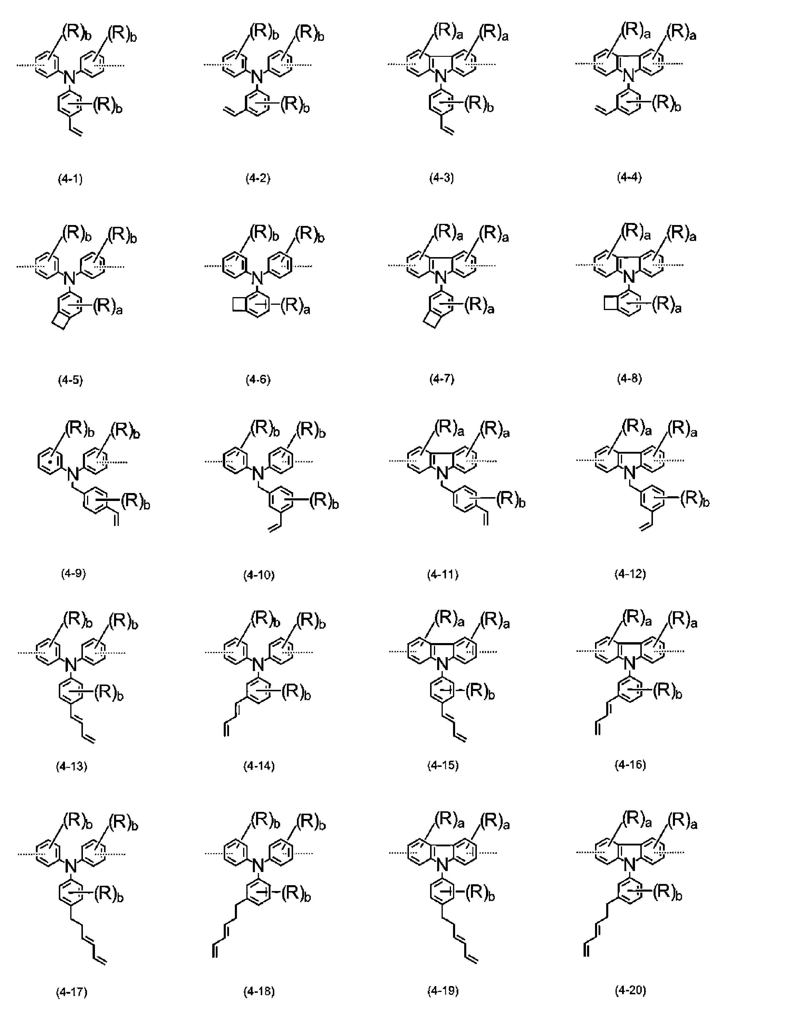

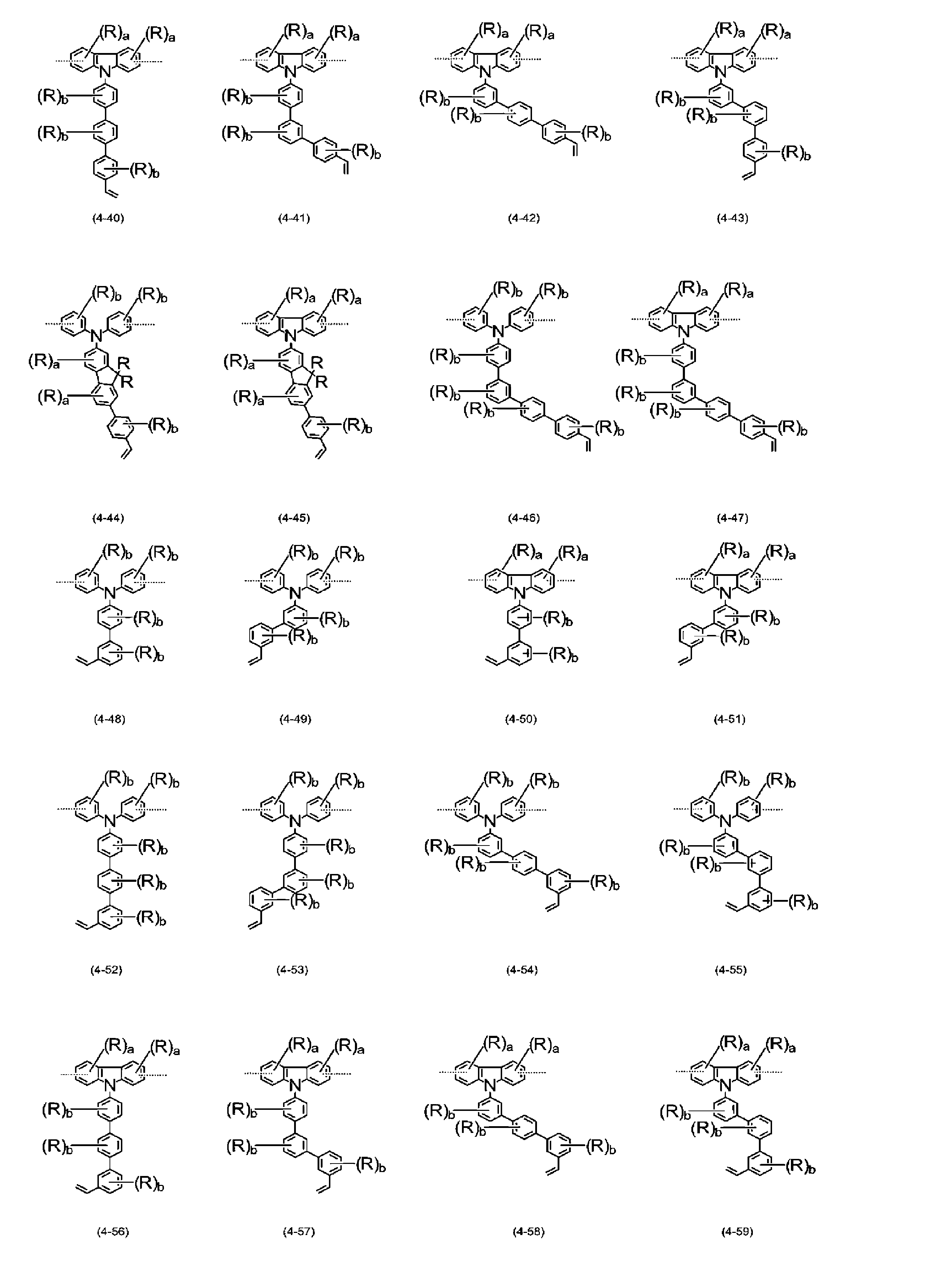



aおよびbは、Rの数であり、以下の整数である。
a=0、1、2または3
b=0、1、2、3または4
(1)正孔の注入特性が良いこと、
(2)正孔の移動度が大きいこと、
(3)ワイドギャップであり、電子阻止能力に優れること、
(4)薄膜状態が安定であること、
という特性を有している。
(1)発光効率および電力効率が高いこと、
(2)実用駆動電圧が低いこと、
(3)長寿命であること、
という利点を有している。
本発明の高分子量化合物が有するトリアリールアミン構造単位および連結構造単位はいずれも2価の基であり、それぞれ下記の一般式(1)および(2)で表される。

アルキルオキシ基(炭素数が1~8)の例としては、メチルオキシ基、エチルオキシ基、n-プロピルオキシ基、イソプロピルオキシ基、n-ブチルオキシ基、tert-ブチルオキシ基、n-ペンチルオキシ基、n-ヘキシルオキシ基、n-ヘプチルオキシ基、n-オクチルオキシ基等が挙げられる。
シクロアルキル基(炭素数が5~10)の例としては、シクロペンチル基、シクロヘキシル基、1-アダマンチル基、2-アダマンチル基等が挙げられる。
シクロアルキルオキシ基(炭素数が5~10)の例としては、シクロペンチルオキシ基、シクロヘキシルオキシ基、シクロヘプチルオキシ基、シクロオクチルオキシ基、1-アダマンチルオキシ基、2-アダマンチルオキシ基等が挙げられる。
アルケニル基(炭素数が2~6)の例としては、ビニル基、アリル基、イソプロペニル基、2-ブテニル基等が挙げられる。
アリールオキシ基(炭素数が6~10)の例としては、フェニルオキシ基、トリルオキシ基等が挙げられる。
a=0、1、2または3
b=0、1、2、3または4
c=0または1
ハロゲン原子、例えば、フッ素原子、塩素原子、臭素原子、およびヨウ素原子;
アルキル基、特に炭素数が1~8のもの、例えば、メチル基、エチル基、n-プロピル基、イソプロピル基、n-ブチル基、イソブチル基、tert-ブチル基、n-ペンチル基、イソペンチル基、ネオペンチル基、n-ヘキシル基、イソへキシル基、ネオへキシル基、n-ヘプチル基、イソへプチル基、ネオへプチル基、n-オクチル基、イソオクチル基、およびネオオクチル基;
アルキルオキシ基、特に炭素数1~8のもの、例えば、メチルオキシ基、エチルオキシ基、およびプロピルオキシ基;
アルケニル基、例えば、ビニル基、およびアリル基;
アリールオキシ基、例えば、フェニルオキシ基、およびトリルオキシ基;
アリール基、例えば、フェニル基、ビフェニリル基、ターフェニリル基、ナフチル基、アントラセニル基、フェナントレニル基、フルオレニル基、インデニル基、ピレニル基、ペリレニル基、フルオランテニル基、およびトリフェニレニル基;
ヘテロアリール基、例えば、ピリジル基、ピリミジニル基、トリアジニル基、チエニル基、フリル基、ピロリル基、キノリル基、イソキノリル基、ベンゾフラニル基、ベンゾチエニル基、インドリル基、カルバゾリル基、インデノカルバゾリル基、ベンゾオキサゾリル基、ベンゾチアゾリル基、キノキサリニル基、ベンゾイミダゾリル基、ピラゾリル基、ジベンゾフラニル基、ジベンゾチエニル基、およびカルボリニル基;
アリールビニル基、例えば、スチリル基、およびナフチルビニル基;
アシル基、例えば、アセチル基、およびベンゾイル基、等が挙げられる。
さらに、これらの置換基は、それぞれ独立して存在していることが好ましいが、これらの置換基同士が、単結合、置換基を有していてもよいメチレン基、酸素原子または硫黄原子を介して、互いに結合して環を形成していてもよい。
上述した一般式(1)で表されるトリアリールアミン構造単位および一般式(2)で表される連結構造単位からなる、一般式(3)で表される繰り返し単位を含む本発明の高分子量化合物は、既に述べたように、正孔の注入特性、正孔の移動度、電子阻止能力、薄膜安定性、耐熱性等の特性が優れているものであるが、これらの特性をより高め、且つ成膜性を確保するという観点から、GPCで測定したポリスチレン換算での重量平均分子量は、好ましくは10,000以上1,000,000未満、より好ましくは10,000以上500,000未満、さらに好ましくは10,000以上200,000未満の範囲である。
また、式中のaおよびbは、Rの数であり、以下の整数である。
a=0、1、2または3
b=0、1、2、3または4
熱架橋性構造単位として、好ましい具体例を示したが、本発明で用いられる熱架橋性構造単位はこれらの構造単位に限定されるものではない。
上述した本発明の高分子量化合物を用いて形成される有機層を備えた有機EL素子は、例えば図3に示す構造を有している。即ち、ガラス基板1(透明樹脂基板など、透明基板であればよい)の上に、透明陽極2、正孔注入層3、正孔輸送層4、発光層5、電子輸送層6および陰極7が設けられている。
銅フタロシアニンに代表されるポルフィリン化合物;
スターバースト型のトリフェニルアミン誘導体;
単結合またはヘテロ原子を含まない2価基で連結した構造を有するアリールアミン(例えば、トリフェニルアミン3量体および4量体);
ヘキサシアノアザトリフェニレンのようなアクセプター性の複素環化合物;
塗布型の高分子材料、例えばポリ(3,4-エチレンジオキシチオフェン)(PEDOT)、ポリ(スチレンスルフォネート)(PSS)等。
ベンジジン誘導体、例えば、
N,N’-ジフェニル-N,N’-ジ(m-トリル)ベンジジン(以下、TPDと略す);
N,N’-ジフェニル-N,N’-ジ(α-ナフチル)ベンジジン(以下、NPDと略す);
N,N,N’,N’-テトラビフェニリルベンジジン;
アミン系誘導体、例えば、
1,1-ビス[4-(ジ-4-トリルアミノ)フェニル]シクロヘキサン(以下、TAPCと略す);
種々のトリフェニルアミン3量体および4量体;
正孔注入層用としても使用される塗布型高分子材料。
カルバゾール誘導体、例えば、
4,4’,4’’-トリ(N-カルバゾリル)トリフェニルアミン(以下、TCTAと略す);
9,9-ビス[4-(カルバゾール-9-イル)フェニル]フルオレン;
1,3-ビス(カルバゾール-9-イル)ベンゼン(以下、mCPと略す);
2,2-ビス(4-カルバゾール-9-イルフェニル)アダマンタン(以下、Ad-Czと略す);
トリアリールアミン構造を有する化合物、例えば、
9-[4-(カルバゾール-9-イル)フェニル]-9-[4-(トリフェニルシリル)フェニル]-9H-フルオレン。
バソクプロイン(以後、BCPと略称する)などのフェナントロリン誘導体;
アルミニウム(III)ビス(2-メチル-8-キノリナート)-4-フェニルフェノレート(以後、BAlqと略称する)などのキノリノール誘導体の金属錯体;
各種希土類錯体;
トリアゾール誘導体;
トリアジン誘導体;
オキサジアゾール誘導体。
なお、以下の説明において、本発明の高分子量化合物が有する一般式(1)で表される構造単位を「構造単位A」、一般式(2)で表される連結構造単位を「構造単位B」、熱架橋性構造単位を「構造単位C」、一般式(1)とは異なるトリアリールアミン構造単位を「構造単位D」として示した。
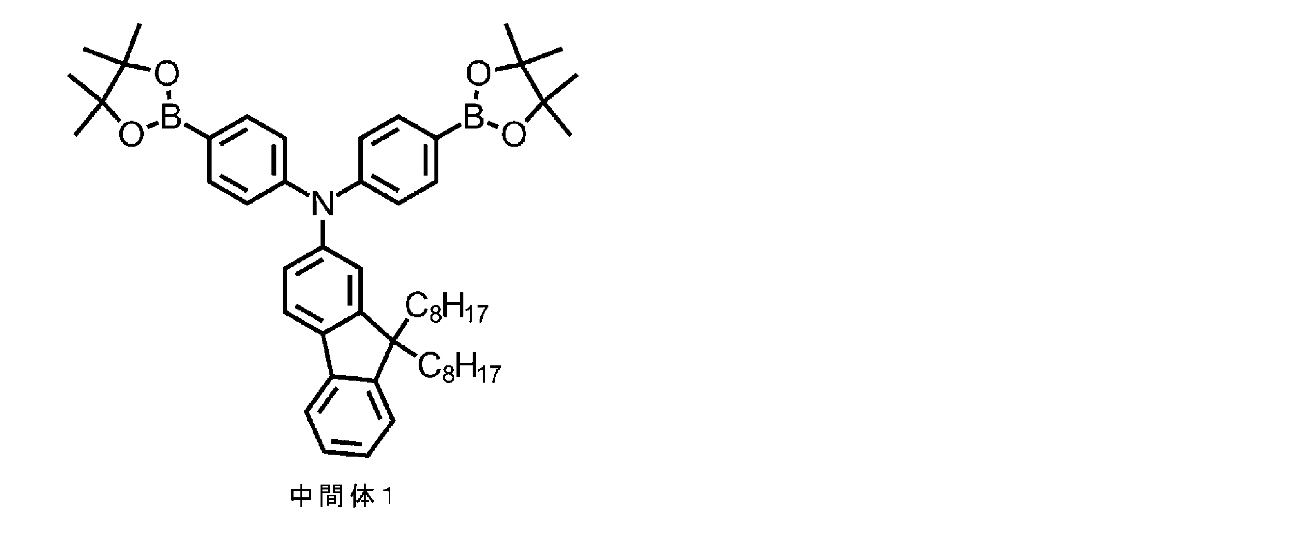
N,N-ビス(4-ブロモフェニル)-9,9-ジ-n-オクチル-9H-フルオレン-2-アミン:16.7g
ビス(ピナコラト)ジボロン:11.9g
酢酸カリウム:5.7g
1,4-ジオキサン:170ml
次いで、{1,1’-ビス(ジフェニルホスフィノ)フェロセン}パラジウム(II)ジクロリドのジクロロメタン付加物0.19gを加えて加熱し、100℃で7時間撹拌した。室温まで冷却した後、水とトルエンを加え、分液操作を行うことによって有機層を採取した。この有機層を無水硫酸ナトリウムで脱水した後、減圧下で濃縮することによって粗製物を得た。粗製物をカラムクロマトグラフィー(酢酸エチル/n-ヘキサン=1/20)で精製することによって中間体1の白色粉体7.6g(収率40%)を得た。
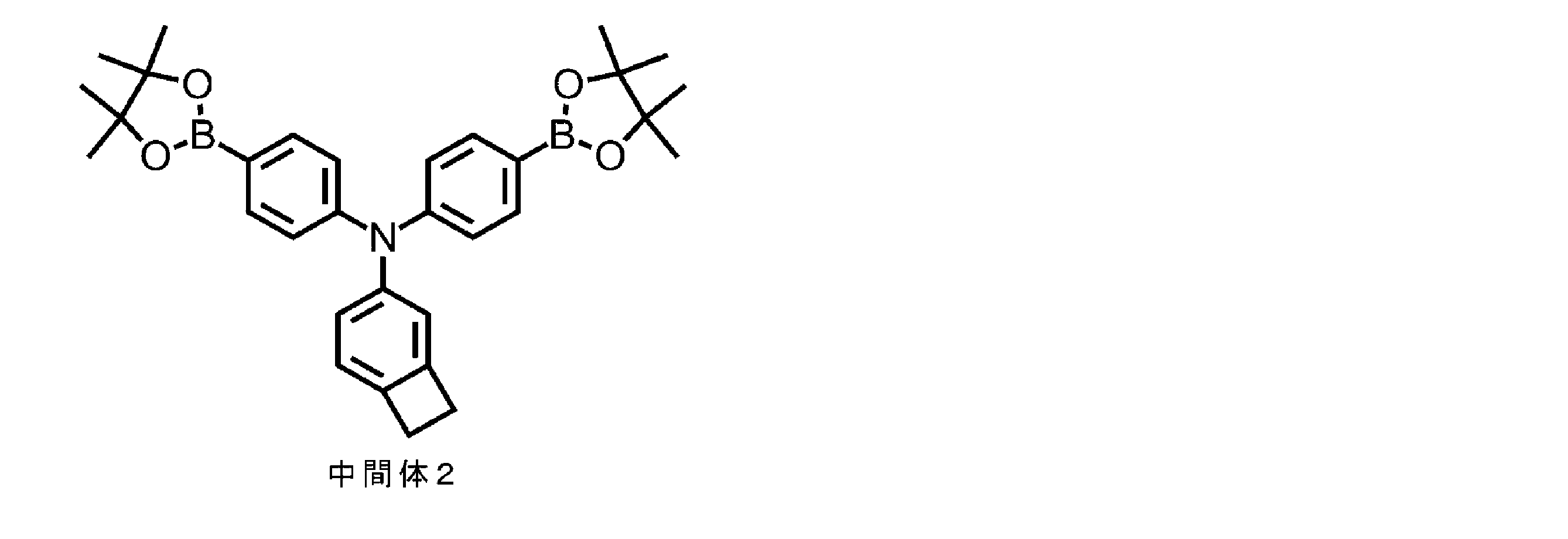
N,N-ビス(4-ブロモフェニル)-N-(ベンゾシクロブテン-4-イル)-アミン:8.0g
ビス(ピナコラト)ジボロン:9.9g
酢酸カリウム:4.6g
1,4-ジオキサン:80ml
次いで、{1,1’-ビス(ジフェニルホスフィノ)フェロセン}パラジウム(II)ジクロリドのジクロロメタン付加物0.3gを加えて加熱し、90℃で11時間撹拌した。室温まで冷却した後、水とトルエンを加え、分液操作を行うことによって有機層を採取した。この有機層を無水硫酸ナトリウムで脱水した後、減圧下で濃縮することによって粗製物を得た。粗製物をトルエン/メタノール=1/2により再結晶することによって、中間体2の白色粉体3.4g(収率35%)を得た。
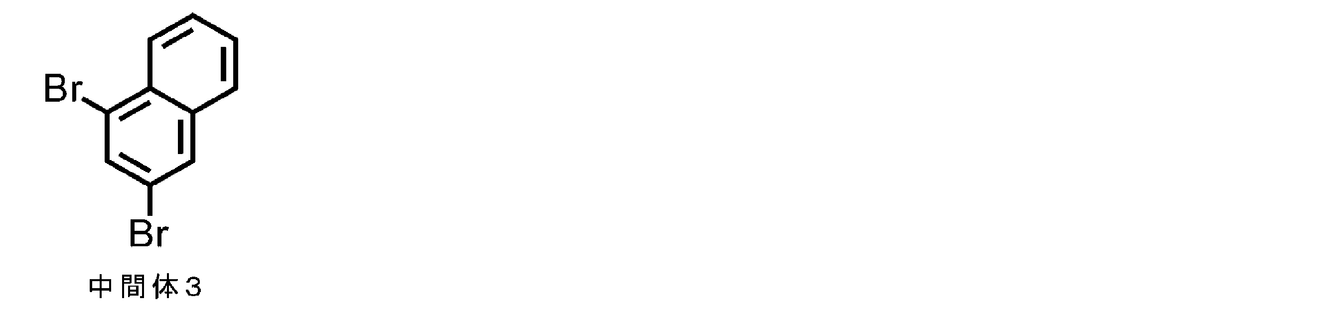
1-アミノ-2,4-ジブロモナフタレン:9.5g
エタノール:320mL
濃硫酸:8.5mL
1.1M亜硝酸ナトリウム水溶液52mLを滴下し、-5℃で1時間撹拌した。その後銅粉:2gを加え、濃硫酸;18.5mLを滴下し、室温で1時間撹拌後、1時間加熱し還流させた。エタノールを留去し、クロロホルムで抽出を行った。得られた有機層を硫酸ナトリウムで乾燥後、乾固し、粗製物をn-ヘキサンを溶離液とするカラムクロマトグラフィーを行った。1つ目のフラクションを回収し、得られた固体に対してエタノールを用いて再結晶を行い、中間体3を白色粉体5.8g(収率65%)として得た。
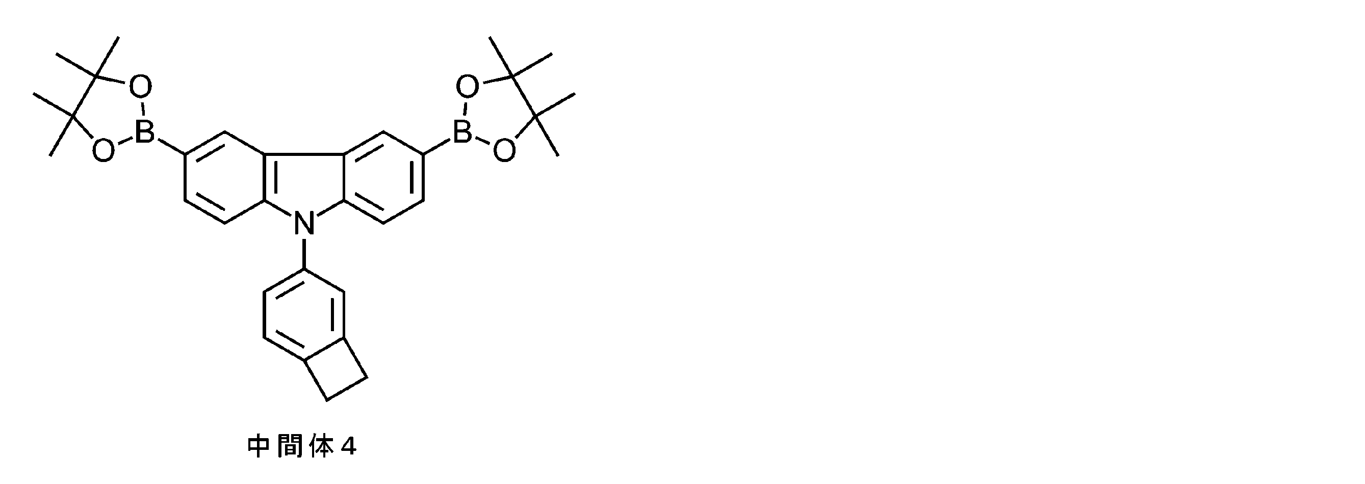
N-(ベンゾシクロブテン-4-イル)-3,6-ジブロモカルバゾール:19.6g
ビス(ピナコラト)ジボロン:24.5g
酢酸カリウム:13.5g
1,4-ジオキサン:120ml
次いで、{1,1’-ビス(ジフェニルホスフィノ)フェロセン}パラジウム(II)ジクロリドのジクロロメタン付加物0.4gを加えて加熱し、97℃で5時間撹拌した。室温まで冷却した後、水とトルエンを加え、分液操作を行うことによって有機層を採取した。この有機層を無水硫酸ナトリウムで脱水した後、減圧下で濃縮することによって粗製物を得た。粗製物をトルエン/メタノール=1/5により再結晶することによって、中間体4の白色粉体14.5g(収率61%)を得た。
高分子量化合物Aの合成;
下記の成分を、窒素置換した反応容器に加え、30分間窒素ガスを通気した。
中間体1:5.6g
中間体2:0.4g
中間体3:2.2g
リン酸三カリウム:6.9g
トルエン:9ml
水:5ml
1,4-ジオキサン:27ml
次いで、酢酸パラジウム(II)を1.4mg、およびトリ-o-トリルホスフィン11.5mgを加えて加熱し、87℃で14時間撹拌した。この後、フェニルボロン酸を17mg加えて1時間撹拌し、次いでブロモベンゼン242mgを加えて1時間撹拌した。トルエン50ml、5wt%N,N-ジエチルジチオカルバミド酸ナトリウム水溶液50mlを加えて加熱し、還流下で2時間撹拌した。室温まで冷却した後、分液操作を行うことによって有機層を採取し、飽和食塩水で3回洗浄した。有機層を無水硫酸ナトリウムで脱水した後、減圧下で濃縮することによって粗ポリマーを得た。粗ポリマーをトルエンに溶解させ、シリカゲルを加えて吸着精製を行い、ろ過してシリカゲルを除去した。得られたろ液を減圧下で濃縮し、乾固物にトルエン100mlを加えて溶解させ、n-ヘキサン300ml中に滴下し、得られた沈殿物を濾取した。この操作を3回繰り返し、乾燥させることにより高分子量化合物Aを3.6g(収率71%)得た。
数平均分子量Mn(ポリスチレン換算):60,000
重量平均分子量Mw(ポリスチレン換算):108,000
分散度(Mw/Mn):1.8
高分子量化合物Bの合成;
下記の成分を、窒素置換した反応容器に加え、30分間窒素ガスを通気した。
中間体1:5.4g
中間体3:2.2g
中間体4:0.5g
リン酸三カリウム:7.4g
トルエン:9ml
水:5ml
1,4-ジオキサン:27ml
次いで、酢酸パラジウム(II)を1.5mg、およびトリ-o-メトキシフェニルホスフィン14.4mgを加えて加熱し、87℃で10時間撹拌した。この後、フェニルボロン酸を163mg加えて1時間撹拌し、次いでブロモベンゼン2.1gを加えて1時間撹拌した。トルエン50ml、5wt%N,N-ジエチルジチオカルバミド酸ナトリウム水溶液50mlを加えて加熱し、還流下で2時間撹拌した。室温まで冷却した後、分液操作を行うことによって有機層を採取し、飽和食塩水で3回洗浄した。有機層を無水硫酸ナトリウムで脱水した後、減圧下で濃縮することによって粗ポリマーを得た。粗ポリマーをトルエンに溶解させ、シリカゲルを加えて吸着精製を行い、ろ過してシリカゲルを除去した。得られたろ液を減圧下で濃縮し、乾固物にトルエン100mlを加えて溶解させ、n-ヘキサン300ml中に滴下し、得られた沈殿物を濾取した。得られた沈殿物にトルエン100mlを加えて溶解させ、n-ヘキサン200ml中に滴下し、得られた沈殿物を濾取した。この操作をあと1回繰り返し、乾燥させることにより高分子量化合物Bを3.2g(収率67%)得た。
数平均分子量Mn(ポリスチレン換算):73,000
重量平均分子量Mw(ポリスチレン換算):139,000
分散度(Mw/Mn):1.9
実施例1および2で合成された高分子量化合物AおよびBを用いて、ITO基板の上に膜厚80nmの塗布膜を作製して、イオン化ポテンシャル測定装置(住友重機械工業株式会社製、PYS-202型)で仕事関数を測定した。その結果は以下の通りであった。
高分子量化合物A:5.63eV
高分子量化合物B:5.61eV
有機EL素子の作製と評価;
図3に示す層構造の有機EL素子を、以下の手法により作製した。
具体的には、膜厚50nmのITOを成膜したガラス基板1を有機溶媒で洗浄した後に、UV/オゾン処理にてITO表面を洗浄した。このガラス基板1に設けられている透明陽極2(ITO)を覆うように、PEDOT/PSS(Ossila製)をスピンコート法により50nmの厚みで成膜し、ホットプレート上、200℃で10分間乾燥して正孔注入層3を形成した。

このように、透明陽極2、正孔注入層3、正孔輸送層4、発光層5、電子輸送層6および陰極7が形成されているガラス基板を、乾燥窒素にて置換したグローブボックス内に移動し、UV硬化樹脂を用いて封止用の他のガラス基板を貼り合わせ、有機EL素子とした。
作製した有機EL素子について、大気中、常温で特性測定を行った。また、作製した有機EL素子に直流電圧を印加したときの発光特性を測定した。測定結果は、表1に示した。
高分子量化合物Aに代えて、下記のTFB(正孔輸送性ポリマー)をトルエンに0.6wt%溶解させて調製された塗布液を用いて正孔輸送層4を形成した以外は、実施例4と同様にして有機EL素子を作製した。


図4に示す層構造の有機EL素子を、以下の手法により作製した。
具体的には、膜厚50nmのITOを成膜したガラス基板8を有機溶媒で洗浄した後に、UV/オゾン処理にてITO表面を洗浄した。このガラス基板8に設けられている透明陽極9(ITO)を覆うように、PEDOT/PSS(Ossila製)をスピンコート法により50nmの厚みで成膜し、ホットプレート上、200℃で10分間乾燥して正孔注入層10を形成した。
このように、透明陽極9、正孔注入層10、正孔輸送層11、電子阻止層12、発光層13、電子輸送層14および陰極15が形成されているガラス基板を、乾燥窒素にて置換したグローブボックス内に移動し、UV硬化樹脂を用いて封止用の他のガラス基板を貼り合わせ、有機EL素子とした。
作製した有機EL素子について、大気中、常温で特性測定を行った。また、作製した有機EL素子に直流電圧を印加したときの発光特性を測定した。測定結果は、表2に示した。
高分子量化合物Aに代えて、実施例2で得られた高分子量化合物Bをトルエンに0.4wt%溶解して調製した塗布液を用いて電子阻止層12を形成した以外は、実施例5と全く同様にして有機EL素子を作製した。作製した有機EL素子について、実施例5と同様に各種特性を評価し、その結果を表2に示した。
図4に示す層構造の有機EL素子を、以下の手法により作製した。
具体的には、膜厚50nmのITOを成膜したガラス基板8を有機溶媒で洗浄した後に、UV/オゾン処理にてITO表面を洗浄した。このガラス基板8に設けられている透明陽極9(ITO)を覆うように、PEDOT/PSS(Ossila製)をスピンコート法により50nmの厚みで成膜し、ホットプレート上、200℃で10分間乾燥して正孔注入層10を形成した。
このように、透明陽極9、正孔注入層10、正孔輸送層11、発光層13、電子輸送層14および陰極15が形成されているガラス基板を、乾燥窒素にて置換したグローブボックス内に移動し、UV硬化樹脂を用いて封止用の他のガラス基板を貼り合わせ、有機EL素子とした。
作製した有機EL素子について、大気中、常温で特性測定を行った。また、作製した有機EL素子に直流電圧を印加したときの発光特性を測定した。測定結果は、表2に示した。
2、9・・・透明陽極
3、10・・・正孔注入層
4、11・・・正孔輸送層
5、13・・・発光層
6、14・・・電子輸送層
7、15・・・陰極
12・・・電子阻止層
Claims (12)
- 下記一般式(1)で表されるトリアリールアミン構造単位、および下記一般式(2)で表される連結構造単位からなる、下記一般式(3)で表される繰り返し構造単位を含み、ポリスチレン換算で10,000以上1,000,000未満の重量平均分子量を有している高分子量化合物。


R2は、それぞれ独立に、炭素数が3~40である、アルキル基、シクロアルキル基、またはアルキルオキシ基を示す。
Xは、水素原子、アミノ基、1価のアリール基、または1価のヘテロアリール基を示す。
Lは、2価のフェニレン基、またはナフチレン基を示し、nは0~3の整数を示す。
a、bおよびcは、R1の数であり、以下の整数である。
a=0、1、2または3
b=0、1、2、3または4
c=0または1 - 前記一般式(1)、(2)および(3)において、a、bおよびcが0である請求項1に記載の高分子量化合物。
- 前記一般式(1)および(3)において、R2が炭素数3~40のアルキル基である請求項1に記載の高分子量化合物。
- 前記一般式(2)および(3)において、Xが水素原子、または置換されていてもよいアミノ基、アリール基、もしくはヘテロアリール基である請求項1に記載の高分子量化合物。
- 前記一般式(2)および(3)において、Xが水素原子、ジフェニルアミノ基、フェニル基、ナフチル基、ジベンゾフラニル基、ジベンゾチエニル基、フェナントレニル基、フルオレニル基、カルバゾリル基、インデノカルバゾリル基、またはアクリジニル基である請求項1に記載の高分子量化合物。
- 熱架橋性構造単位、または前記一般式(1)で表されるトリアリールアミン構造単位とは異なるトリアリールアミン構造単位を含む請求項1に記載の高分子量化合物。
- 前記熱架橋性構造単位が下記一般式(4-1)~(4-143)に示す構造単位である請求項6に記載の高分子量化合物。


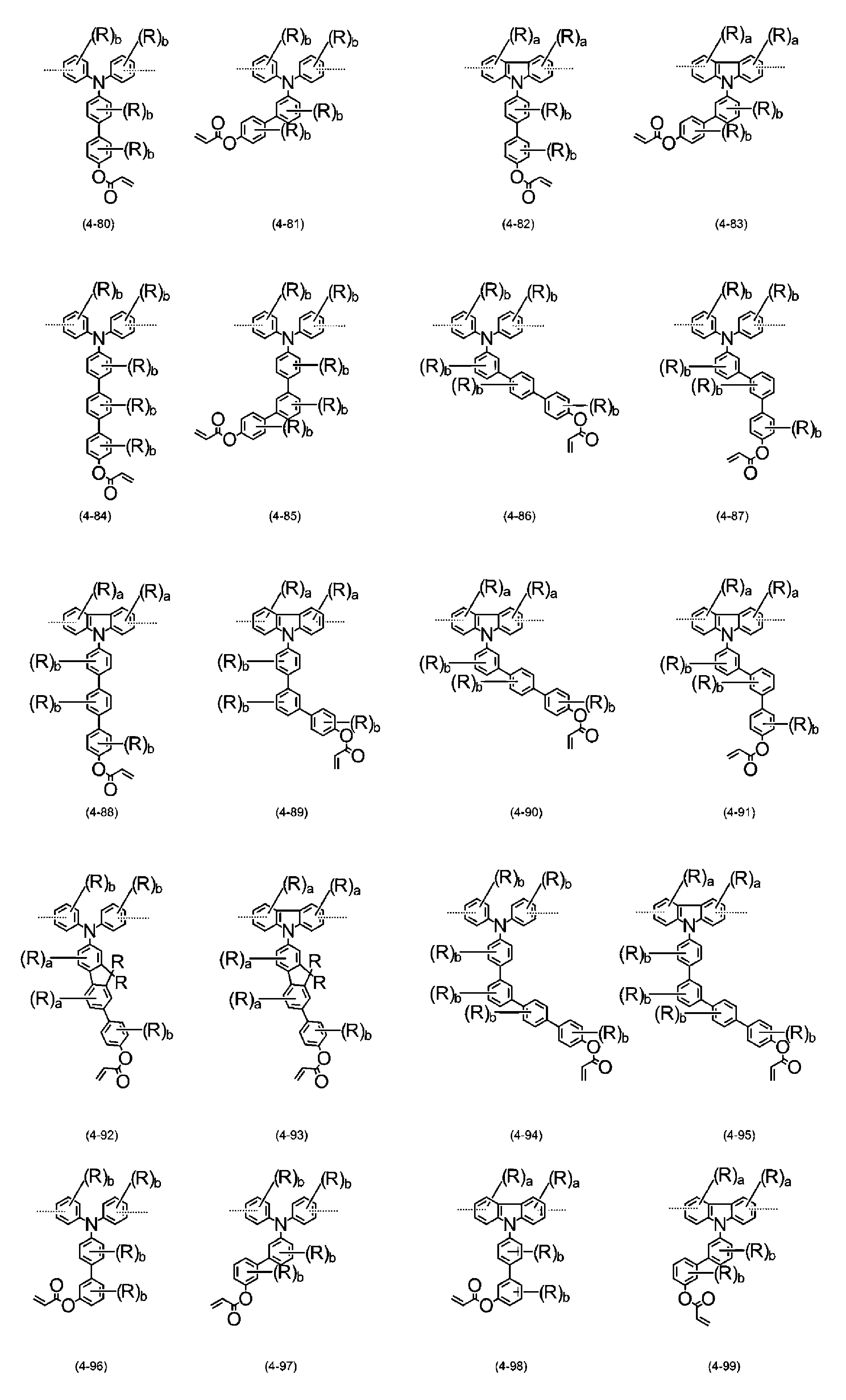
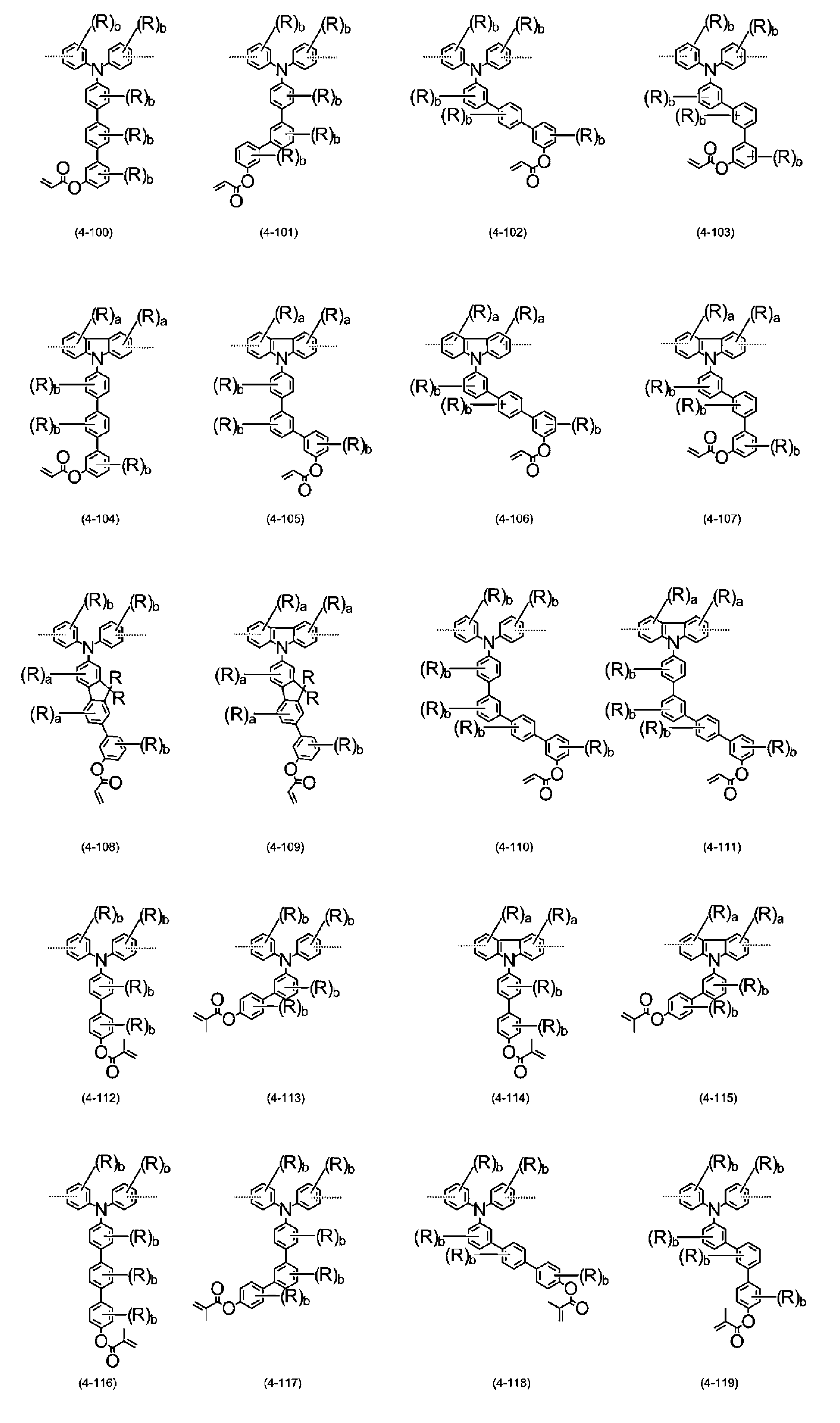


式中、Rは、それぞれ独立に、水素原子、重水素原子、シアノ基、ニトロ基、フッ素原子、塩素原子、臭素原子、ヨウ素原子、または炭素数が3~40である、アルキル基、シクロアルキル基、アルキルオキシ基、シクロアルキルオキシ基、アルケニル基、もしくはアリールオキシ基を示す。
aおよびbは、Rの数であり、以下の整数である。
a=0、1、2または3
b=0、1、2、3または4
前記式(4-1)~(4-143)において、破線は、隣接する構造単位への結合手を示し、環から延びている先端がフリーの実線は、その先端がメチル基であることを示している。 - 請求項1~7のいずれか1項に記載の高分子量化合物を用いて形成される有機層を備えた有機エレクトロルミネッセンス素子。
- 前記有機層が正孔輸送層である、請求項8に記載の有機エレクトロルミネッセンス素子。
- 前記有機層が電子阻止層である、請求項8に記載の有機エレクトロルミネッセンス素子。
- 前記有機層が正孔注入層である、請求項8に記載の有機エレクトロルミネッセンス素子。
- 前記有機層が発光層である、請求項8に記載の有機エレクトロルミネッセンス素子。
Priority Applications (3)
| Application Number | Priority Date | Filing Date | Title |
|---|---|---|---|
| JP2024504733A JPWO2023167253A1 (ja) | 2022-03-04 | 2023-03-01 | |
| KR1020247015836A KR20240155182A (ko) | 2022-03-04 | 2023-03-01 | 트리아릴아민 고분자량 화합물 및 유기 일렉트로 루미네선스 소자 |
| CN202380014569.0A CN118265737A (zh) | 2022-03-04 | 2023-03-01 | 三芳基胺高分子量化合物以及有机电致发光元件 |
Applications Claiming Priority (2)
| Application Number | Priority Date | Filing Date | Title |
|---|---|---|---|
| JP2022033606 | 2022-03-04 | ||
| JP2022-033606 | 2022-03-04 |
Publications (1)
| Publication Number | Publication Date |
|---|---|
| WO2023167253A1 true WO2023167253A1 (ja) | 2023-09-07 |
Family
ID=87883847
Family Applications (1)
| Application Number | Title | Priority Date | Filing Date |
|---|---|---|---|
| PCT/JP2023/007667 Ceased WO2023167253A1 (ja) | 2022-03-04 | 2023-03-01 | トリアリールアミン高分子量化合物および有機エレクトロルミネッセンス素子 |
Country Status (5)
| Country | Link |
|---|---|
| JP (1) | JPWO2023167253A1 (ja) |
| KR (1) | KR20240155182A (ja) |
| CN (1) | CN118265737A (ja) |
| TW (1) | TW202342578A (ja) |
| WO (1) | WO2023167253A1 (ja) |
Citations (12)
| Publication number | Priority date | Publication date | Assignee | Title |
|---|---|---|---|---|
| JP2009043896A (ja) * | 2007-08-08 | 2009-02-26 | Canon Inc | 有機発光素子及びディスプレイ |
| JP2010062442A (ja) * | 2008-09-05 | 2010-03-18 | Canon Inc | 有機発光素子 |
| WO2017086357A1 (ja) * | 2015-11-17 | 2017-05-26 | 保土谷化学工業株式会社 | 有機エレクトロルミネッセンス素子 |
| WO2018101331A1 (ja) * | 2016-11-30 | 2018-06-07 | 保土谷化学工業株式会社 | 置換トリアリールアミン構造単位を含む高分子量化合物 |
| WO2018168667A1 (ja) * | 2017-03-15 | 2018-09-20 | 保土谷化学工業株式会社 | 置換トリアリールアミン骨格を有する高分子量化合物 |
| WO2020009069A1 (ja) * | 2018-07-03 | 2020-01-09 | 保土谷化学工業株式会社 | 分子主鎖にターフェニル構造を含むトリアリールアミン高分子量化合物およびこれらの高分子量化合物を含む有機エレクトロルミネッセンス素子 |
| WO2020127176A1 (en) * | 2018-12-20 | 2020-06-25 | Merck Patent Gmbh | Materials for electronic devices |
| WO2020246404A1 (ja) * | 2019-06-05 | 2020-12-10 | 保土谷化学工業株式会社 | 置換トリアリールアミン構造単位を含む高分子量化合物および有機エレクトロルミネッセンス素子 |
| WO2021040328A1 (ko) * | 2019-08-23 | 2021-03-04 | 주식회사 엘지화학 | 유기 발광 소자 |
| WO2021070878A1 (ja) * | 2019-10-09 | 2021-04-15 | 保土谷化学工業株式会社 | 高分子量化合物からなる有機層を有する有機エレクトロルミネッセンス素子 |
| JP2021517923A (ja) * | 2018-08-17 | 2021-07-29 | エルジー・ケム・リミテッド | 重合体、これを含むコーティング組成物およびこれを用いた有機発光素子 |
| WO2021166921A1 (ja) * | 2020-02-20 | 2021-08-26 | 保土谷化学工業株式会社 | 高分子量化合物および該高分子量化合物を含む発光ダイオード |
Family Cites Families (7)
| Publication number | Priority date | Publication date | Assignee | Title |
|---|---|---|---|---|
| US6309763B1 (en) | 1997-05-21 | 2001-10-30 | The Dow Chemical Company | Fluorene-containing polymers and electroluminescent devices therefrom |
| CN1894199B (zh) | 2003-11-14 | 2011-04-13 | 住友化学株式会社 | 卤代双二芳基氨基多环芳族化合物及其聚合物 |
| GB0329364D0 (en) | 2003-12-19 | 2004-01-21 | Cambridge Display Tech Ltd | Optical device |
| JP4736471B2 (ja) | 2004-02-26 | 2011-07-27 | 住友化学株式会社 | 高分子化合物およびそれを用いた高分子発光素子 |
| JP2007119763A (ja) | 2005-09-29 | 2007-05-17 | Sumitomo Chemical Co Ltd | 高分子材料及び高分子発光素子 |
| JP5217153B2 (ja) | 2005-11-18 | 2013-06-19 | 住友化学株式会社 | 高分子化合物およびそれを用いた高分子発光素子 |
| JP5018043B2 (ja) | 2005-12-01 | 2012-09-05 | 住友化学株式会社 | 高分子化合物およびそれを用いた高分子発光素子 |
-
2023
- 2023-03-01 JP JP2024504733A patent/JPWO2023167253A1/ja active Pending
- 2023-03-01 KR KR1020247015836A patent/KR20240155182A/ko active Pending
- 2023-03-01 CN CN202380014569.0A patent/CN118265737A/zh active Pending
- 2023-03-01 WO PCT/JP2023/007667 patent/WO2023167253A1/ja not_active Ceased
- 2023-03-02 TW TW112107499A patent/TW202342578A/zh unknown
Patent Citations (12)
| Publication number | Priority date | Publication date | Assignee | Title |
|---|---|---|---|---|
| JP2009043896A (ja) * | 2007-08-08 | 2009-02-26 | Canon Inc | 有機発光素子及びディスプレイ |
| JP2010062442A (ja) * | 2008-09-05 | 2010-03-18 | Canon Inc | 有機発光素子 |
| WO2017086357A1 (ja) * | 2015-11-17 | 2017-05-26 | 保土谷化学工業株式会社 | 有機エレクトロルミネッセンス素子 |
| WO2018101331A1 (ja) * | 2016-11-30 | 2018-06-07 | 保土谷化学工業株式会社 | 置換トリアリールアミン構造単位を含む高分子量化合物 |
| WO2018168667A1 (ja) * | 2017-03-15 | 2018-09-20 | 保土谷化学工業株式会社 | 置換トリアリールアミン骨格を有する高分子量化合物 |
| WO2020009069A1 (ja) * | 2018-07-03 | 2020-01-09 | 保土谷化学工業株式会社 | 分子主鎖にターフェニル構造を含むトリアリールアミン高分子量化合物およびこれらの高分子量化合物を含む有機エレクトロルミネッセンス素子 |
| JP2021517923A (ja) * | 2018-08-17 | 2021-07-29 | エルジー・ケム・リミテッド | 重合体、これを含むコーティング組成物およびこれを用いた有機発光素子 |
| WO2020127176A1 (en) * | 2018-12-20 | 2020-06-25 | Merck Patent Gmbh | Materials for electronic devices |
| WO2020246404A1 (ja) * | 2019-06-05 | 2020-12-10 | 保土谷化学工業株式会社 | 置換トリアリールアミン構造単位を含む高分子量化合物および有機エレクトロルミネッセンス素子 |
| WO2021040328A1 (ko) * | 2019-08-23 | 2021-03-04 | 주식회사 엘지화학 | 유기 발광 소자 |
| WO2021070878A1 (ja) * | 2019-10-09 | 2021-04-15 | 保土谷化学工業株式会社 | 高分子量化合物からなる有機層を有する有機エレクトロルミネッセンス素子 |
| WO2021166921A1 (ja) * | 2020-02-20 | 2021-08-26 | 保土谷化学工業株式会社 | 高分子量化合物および該高分子量化合物を含む発光ダイオード |
Also Published As
| Publication number | Publication date |
|---|---|
| KR20240155182A (ko) | 2024-10-28 |
| CN118265737A (zh) | 2024-06-28 |
| JPWO2023167253A1 (ja) | 2023-09-07 |
| TW202342578A (zh) | 2023-11-01 |
Similar Documents
| Publication | Publication Date | Title |
|---|---|---|
| JP7421476B2 (ja) | 分子主鎖にターフェニル構造を含むトリアリールアミン高分子量化合物およびこれらの高分子量化合物を含む有機エレクトロルミネッセンス素子 | |
| JP7017558B2 (ja) | 置換トリアリールアミン骨格を有する高分子量化合物 | |
| JP6942724B2 (ja) | 置換トリアリールアミン構造単位を含む高分子量化合物 | |
| JP7523873B2 (ja) | 置換トリアリールアミン構造単位を含む高分子量化合物および有機エレクトロルミネッセンス素子 | |
| JP7579268B2 (ja) | 高分子量化合物からなる有機層を有する有機エレクトロルミネッセンス素子 | |
| US20240260288A1 (en) | High molecular weight triarylamine compounds, and organic electroluminescent elements containing these high molecular weight compounds | |
| JP7824212B2 (ja) | 高分子量化合物および該高分子量化合物を含む発光ダイオード | |
| JP2024127866A (ja) | 高分子量化合物および有機エレクトロルミネッセンス素子 | |
| JP7783251B2 (ja) | インデノジベンゾヘテロール構造を部分構造として有する高分子量化合物、およびこれらの高分子量化合物を含む有機エレクトロルミネッセンス素子 | |
| JP2023022389A (ja) | スピロビフルオレン化合物および有機エレクトロルミネッセンス素子 | |
| WO2023167253A1 (ja) | トリアリールアミン高分子量化合物および有機エレクトロルミネッセンス素子 | |
| JP7791827B2 (ja) | 熱架橋性低分子化合物を含む発光ダイオード用組成物 | |
| JP2024052606A (ja) | 高分子量化合物およびこれらを用いた有機エレクトロルミネッセンス素子 | |
| WO2023182377A1 (ja) | トリアリールアミン高分子量化合物および有機エレクトロルミネッセンス素子 | |
| JP2024008856A (ja) | 高分子量化合物およびこれらを用いた有機エレクトロルミネッセンス素子 |
Legal Events
| Date | Code | Title | Description |
|---|---|---|---|
| 121 | Ep: the epo has been informed by wipo that ep was designated in this application |
Ref document number: 23763510 Country of ref document: EP Kind code of ref document: A1 |
|
| ENP | Entry into the national phase |
Ref document number: 2024504733 Country of ref document: JP Kind code of ref document: A |
|
| WWE | Wipo information: entry into national phase |
Ref document number: 202380014569.0 Country of ref document: CN |
|
| NENP | Non-entry into the national phase |
Ref country code: DE |
|
| 122 | Ep: pct application non-entry in european phase |
Ref document number: 23763510 Country of ref document: EP Kind code of ref document: A1 |