WO2023163018A1 - 光計測装置 - Google Patents
光計測装置 Download PDFInfo
- Publication number
- WO2023163018A1 WO2023163018A1 PCT/JP2023/006392 JP2023006392W WO2023163018A1 WO 2023163018 A1 WO2023163018 A1 WO 2023163018A1 JP 2023006392 W JP2023006392 W JP 2023006392W WO 2023163018 A1 WO2023163018 A1 WO 2023163018A1
- Authority
- WO
- WIPO (PCT)
- Prior art keywords
- optical
- light
- frequency
- interference
- pulse train
- Prior art date
- Legal status (The legal status is an assumption and is not a legal conclusion. Google has not performed a legal analysis and makes no representation as to the accuracy of the status listed.)
- Ceased
Links
Images





Classifications
-
- G—PHYSICS
- G01—MEASURING; TESTING
- G01N—INVESTIGATING OR ANALYSING MATERIALS BY DETERMINING THEIR CHEMICAL OR PHYSICAL PROPERTIES
- G01N21/00—Investigating or analysing materials by the use of optical means, i.e. using sub-millimetre waves, infrared, visible or ultraviolet light
- G01N21/17—Systems in which incident light is modified in accordance with the properties of the material investigated
- G01N21/25—Colour; Spectral properties, i.e. comparison of effect of material on the light at two or more different wavelengths or wavelength bands
- G01N21/27—Colour; Spectral properties, i.e. comparison of effect of material on the light at two or more different wavelengths or wavelength bands using photo-electric detection ; circuits for computing concentration
-
- G—PHYSICS
- G01—MEASURING; TESTING
- G01B—MEASURING LENGTH, THICKNESS OR SIMILAR LINEAR DIMENSIONS; MEASURING ANGLES; MEASURING AREAS; MEASURING IRREGULARITIES OF SURFACES OR CONTOURS
- G01B9/00—Measuring instruments characterised by the use of optical techniques
- G01B9/02—Interferometers
- G01B9/0209—Low-coherence interferometers
- G01B9/02091—Tomographic interferometers, e.g. based on optical coherence
-
- G—PHYSICS
- G01—MEASURING; TESTING
- G01B—MEASURING LENGTH, THICKNESS OR SIMILAR LINEAR DIMENSIONS; MEASURING ANGLES; MEASURING AREAS; MEASURING IRREGULARITIES OF SURFACES OR CONTOURS
- G01B9/00—Measuring instruments characterised by the use of optical techniques
- G01B9/02—Interferometers
- G01B9/02001—Interferometers characterised by controlling or generating intrinsic radiation properties
- G01B9/02007—Two or more frequencies or sources used for interferometric measurement
- G01B9/02008—Two or more frequencies or sources used for interferometric measurement by using a frequency comb
-
- G—PHYSICS
- G01—MEASURING; TESTING
- G01N—INVESTIGATING OR ANALYSING MATERIALS BY DETERMINING THEIR CHEMICAL OR PHYSICAL PROPERTIES
- G01N21/00—Investigating or analysing materials by the use of optical means, i.e. using sub-millimetre waves, infrared, visible or ultraviolet light
- G01N21/62—Systems in which the material investigated is excited whereby it emits light or causes a change in wavelength of the incident light
- G01N21/63—Systems in which the material investigated is excited whereby it emits light or causes a change in wavelength of the incident light optically excited
- G01N21/65—Raman scattering
Definitions
- the present invention relates to an optical measurement device.
- This application claims priority based on Japanese Patent Application No. 2022-026953 filed in Japan on February 24, 2022, the content of which is incorporated herein.
- optical frequency combs An ultrashort pulse train in which optical frequency mode trains whose spectral intensities are precisely arranged in a comb-like pattern at equal intervals on the frequency axis are phase-synchronized with each other and whose absolute values are completely controlled are called "optical frequency combs". ' or simply 'optical comb'.
- optical frequency combs For example, on the frequency axis of a mode-locked laser, which is an ultrashort pulse laser, a large number of optical frequency mode trains appear at regular intervals, and the optical frequency modes are phase-locked with each other. When this optical frequency is perfectly controlled, this light source becomes an optical comb. Since the optical frequency can be controlled using an extremely accurate clock such as an atomic clock, it is widely used as a precise measure of optical frequency and distance (see, for example, Non-Patent Document 1).
- optical frequency combs have been used as light sources that are stabilized with high accuracy. That is, it can be said that the optical frequency comb is a coherent pulse train with low jitter in the time domain, and a comb-like spectrum that is accurately mode-resolved in the frequency domain.
- the carrier envelope offset frequency and repetition frequency (frequency interval) of such an optical frequency comb, the carrier envelope offset frequency difference when using two optical frequency combs, and the repetition frequency difference have been treated as fixed parameters. .
- optical measurement is widely used in fields such as distance measurement, shape measurement, and spectroscopy.
- a basic measurement method in such optical measurement is to irradiate an object to be measured with measurement light and measure its transmitted light and reflected light.
- multiple reflection of the measurement light from the object to be measured may result in extra light (background light) other than the light to be originally measured.
- background light extra light
- you want to measure the internal reflection of an object under test you want to observe a weak nonlinear signal that produces surface reflected light that is stronger than the internal reflected light on the surface of the object under test. problems such as the observation of a large amount of transmitted light. When such strong background light exists, the light that is originally intended to be measured may be buried.
- the delay time difference between the light to be originally measured and the background light is used to separate the light in time, or the deviation of the optical axis between the light to be originally measured and the background light is used. have been used to separate them spatially.
- the background light cannot be effectively removed by the temporal and spatial separating means. there were.
- the present invention has been made in view of the above circumstances, and provides an optical measurement device capable of removing background light in optical measurement using high controllability of an optical frequency comb.
- An embodiment of the present invention comprises a predetermined carrier envelope offset frequency with respect to zero on the frequency axis, and a plurality of frequencies arranged at intervals of integral multiples of a predetermined repetition frequency on the frequency axis based on the carrier envelope offset frequency.
- a pulse interval based on the repetition frequency of the optical frequency comb generated by the light source; an inter-pulse phase difference based on the carrier envelope offset frequency and the repetition frequency; and a second optical path for guiding measurement result light obtained from the measurement object irradiated with the optical pulse train guided by the first optical path, a third optical path guiding delayed light obtained by delaying the optical pulse train by a delay time corresponding to the pulse interval; the measurement result light guided by the second optical path; and the third optical path guiding light.
- an interference unit that interferes with the delayed light
- a control unit that variably controls at least one of the carrier envelope offset frequency and the repetition frequency of the light source based on the state of the light after interference by the interference unit;
- An optical measurement device comprising
- the optical measurement device described above further includes an acquisition unit that acquires at least one of the amplitude and frequency of the light after interference as the state of the light, and the control unit and variably controlling at least one of the carrier envelope offset frequency and the repetition frequency of the light source based on the result of obtaining the state of light by the obtaining unit and information indicating the reference of the state of light. .
- control unit sweep-variably controls at least one of the carrier envelope offset frequency and the repetition frequency of the light source, so that the optical pulse train to change the pulse interval and the inter-pulse phase difference.
- control unit changes the repetition frequency without changing the ratio between the carrier envelope offset frequency and the repetition frequency, thereby changing the The pulse interval of the optical pulse train is varied.
- the controller changes the inter-pulse phase difference of the optical pulse train by changing the ratio between the carrier envelope offset frequency and the repetition frequency. change.
- the optical measurement device described above further includes a measurement unit that measures the light after interference by the interference unit as signal light.
- a second interference section that causes interference between the reference light of the optical pulse train based on the optical pulse train and the measurement result light or the light after interference by the interference section and a second measurement section that measures the light interfered by the second interference section as signal light.
- background light can be selectively removed in optical measurement using an optical frequency comb.
- FIG. 1A is a diagram showing a correspondence relationship between a waveform in the time domain and a spectral distribution in the frequency domain for an optical frequency comb.
- the output from a mode-locked laser is a periodic pulse train in the time domain, which can be visualized as a function of the fast oscillating electric field and envelope.
- an optical comb having optical frequency mode groups evenly spaced on the frequency axis can be completely represented by two frequencies called repetition frequency (frep) and carrier envelope frequency (fceo).
- the repetition frequency represents the interval of each optical frequency mode, and represents the pulse-to-pulse distance of the ultrashort pulse train on the time axis.
- An example of an ultrashort pulse is shown in FIG. 1B.
- the carrier envelope frequency is expressed as a deviation (offset) that occurs when the optical frequency mode string on the frequency axis is repeatedly extended to DC. Considering this on the time axis, it represents the carrier phase difference between each pulse of the pulse train.
- the carrier phase is called a so-called carrier-envelope offset phase (CEP, also referred to as carrier phase in the following description).
- CEP carrier-envelope offset phase
- Each carrier phase ( ⁇ n) of the pulse train on the time axis changes by a constant phase amount for each pulse, and as a result has a constant cycle (carrier phase cycle Tceo).
- a relative carrier phase difference between adjacent pulse trains on the time axis is also called an inter-pulse phase difference.
- the reciprocal of the carrier phase period Tceo is the carrier envelope offset frequency fceo on the frequency axis.
- the reciprocal of the pulse repetition period (pulse interval) Trep is the repetition frequency (frequency interval) frep.
- the longitudinal mode (optical frequency mode) of the laser is extremely uniformly distributed at the repetition frequency (frequency interval) frep interval.
- the carrier envelope offset frequency fceo and the repetition frequency frep are related by using the inter-pulse phase difference ( ⁇ n+1 ⁇ n) as shown in Equation (3).
- the repetition frequency frep and the carrier envelope offset frequency fceo in the optical frequency comb are important frequency parameters that indicate the characteristics of the pulse train.
- the degree of freedom in controlling the repetition frequency frep and the carrier envelope offset frequency fceo is actively utilized.
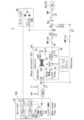
- FIG. 2 is a diagram showing an example of the configuration of the optical measurement device 1 of this embodiment.
- the optical measurement device 1 includes a light source 10 , a measurement section 20 , a measurement section 30 and an acquisition section 40 .
- the light source 10 is, for example, a mode-locked laser light source and generates an optical frequency comb.
- This optical frequency comb has a predetermined carrier envelope offset frequency fceo with respect to zero on the frequency axis, and a plurality of frequency modes arranged at intervals of integral multiples of a predetermined repetition frequency frep based on the carrier envelope offset frequency fceo on the frequency axis. and
- the light source 10 outputs an optical pulse train L1 generated by the optical frequency comb to the measuring section 20 .
- the optical pulse train L1 has a pulse interval Trep based on the repetition frequency frep of the optical frequency comb generated by the light source 10 and an inter-pulse phase difference ( ⁇ n+1 ⁇ n) based on the carrier envelope offset frequency fceo and the repetition frequency frep.
- the measuring section 20 includes a first optical path 21 , a second optical path 22 , a third optical path 23 and an interference section 24 .
- the first optical path 21 guides the optical pulse train L1 to the measurement object 25 .
- the second optical path 22 guides the measurement result light L2 obtained from the measurement object 25 irradiated with the light pulse train L1 guided by the first optical path 21 .
- the third optical path 23 guides delayed light L3 obtained by delaying the optical pulse train L1 by a delay time corresponding to the pulse interval Trep.
- the measurement section 20 includes a delay section 230 on the third optical path 23 .
- the delay section 230 comprises an optical delay circuit based on spatial optics such as a multi-pass cavity (MPC).
- MPC multi-pass cavity
- the delay unit 230 may have any configuration as shown in FIGS. 3 and 4, for example, as long as the frequency dependence (dispersion) of delay can be adjusted.
- FIG. 3 is a diagram showing a first modification of the configuration of the delay section of this embodiment.
- the delay unit 232 of the first modification includes an optical delay circuit using an optical fiber.
- FIG. 4 is a diagram showing a second modification of the configuration of the delay section of this embodiment.
- the delay section 233 of the second modification includes an optical delay circuit using a waveguide (for example, arrayed waveguide gratings; AWG).
- the interference unit 24 causes the measurement result light L2 guided by the second optical path 22 and the delayed light L3 guided by the third optical path 23 to interfere.
- the measurement unit 30 measures the light L4 after interference by the interference unit 24 as the signal light L5.
- the signal light L5 is guided to the OSA by the SMF and the spectrum is measured, but other optical systems and measuring devices may be used depending on the object to be measured.
- the acquisition unit 40 acquires at least one of the amplitude and frequency of the light L4 after interference as the state of light.
- the light source 10 has a control section 100 .
- the control unit 100 variably controls at least one of the carrier envelope offset frequency fceo and the repetition frequency frep of the light source 10 based on the state of the light L4 after interference by the interference unit 24 .
- the optical pulse train L1 is divided into two optical paths, the first optical path 21 and the third optical path 23, and a delay is given to the pulsed light on one of the optical paths (that is, the third optical path 23), the first optical path 21 A desired phase difference pulse pair can be generated between the pulsed light (that is, the measurement result light L2) and the pulsed light (that is, the delayed light L3) of the third optical path 23.
- the inter-pulse phase difference ( ⁇ n+1 ⁇ n) corresponding to the delay time of the third optical path 23 is set so that the measurement result light L2 of the first optical path 21 and the delayed light L3 of the third optical path 23 have opposite phases.
- the background light included in the measurement result light L2 can be removed by applying it to the pulse train L1 and causing the measurement result light L2 and the delayed light L3 to interfere with each other. That is, the background light of the measurement result light L2 can be removed by changing the ratio of the repetition frequency frep and the carrier envelope offset frequency fceo to control the inter-pulse phase difference ( ⁇ n+1 ⁇ n) of the optical pulse train L1. .
- control unit 100 may feedback-control at least one of the carrier envelope offset frequency fceo and the repetition frequency frep based on the state of the light L4 after interference.
- the mutual frequency ratio may be fixed, or the absolute frequency may be fixed.
- a circuit using a frequency divider, a mixer, or the like shown in the control section 100 may be used to set the frequency ratio between the repetition frequency and the carrier envelope offset frequency to a predetermined frequency ratio.
- the frequency may be measured using a microprocessor such as FPGA.
- control unit 100 determines at least one of the carrier envelope offset frequency fceo and the repetition frequency frep of the light source 10 based on the result of obtaining the state of light by the obtaining unit 40 and the information indicating the reference of the state of light. Variable control.
- the optical measurement device 1 of the present embodiment may be a transmission type measurement device that measures transmitted light, or may be a reflection type measurement device that measures reflected light.
- control by control unit 100 an example of control by the control unit 100 will be described.
- the background light is given dispersion by the measurement object 25 . Therefore, the background light may not be sufficiently removed simply by causing the delayed light L3 to interfere with the light L4 after interference.
- the control unit 100 of the present embodiment sweep-variably controls the state of the delayed light L3 that interferes with the light L4 after interference.
- the control unit 100 sweeps and variably controls at least one of the carrier envelope offset frequency fceo and the repetition frequency frep of the light source 10 to change the pulse interval Trep and the inter-pulse phase difference ( ⁇ n+1 ⁇ n) of the optical pulse train L1.
- the sweep variable control of the state of the delayed light L3 can be achieved by variably controlling the parameters of the optical pulse train L1 (carrier envelope offset frequency fceo and repetition frequency frep), and variable control by mechanical parts is unnecessary. Therefore, according to the control unit 100 configured in this way, it is possible to suppress the occurrence of control errors due to the mass and accuracy of mechanical parts, and to remove the background light that has the effect of dispersing the measurement target 25 .
- the control unit 100 changes the pulse interval Trep of the optical pulse train L1 by changing the repetition frequency frep without changing the ratio between the carrier envelope offset frequency fceo and the repetition frequency frep.
- the control unit 100 variably controls the repetition frequency frep with respect to the state change of the light L4 after interference due to environmental fluctuations, and performs feedback control to cancel the influence of the environmental fluctuations.
- the control unit 100 configured in this way it is possible to reduce the change in the state of the light L4 after interference due to environmental fluctuations, and to make the minute signal light L5 stand out. That is, according to the control unit 100 configured in this manner, the optical measurement device 1 having higher robustness against changes in the changing environment can be realized.
- the control unit 100 changes the ratio between the carrier envelope offset frequency fceo and the repetition frequency frep to control the interpulse phase difference ( ⁇ n+1 ⁇ n) of the optical pulse train L1. ).
- the control unit 100 variably controls the repetition frequency frep in response to a change in the state of the light L4 after interference due to environmental fluctuations, and performs feedback control to cancel the influence of the environmental fluctuations.
- the ratio to the repetition frequency frep is changed. According to the control unit 100 configured in this way, it is possible to perform sweep variable control of the inter-pulse phase difference ( ⁇ n+1 ⁇ n) of the optical pulse train L1 while reducing the state change of the light L4 after interference due to environmental fluctuations. can.
- FIG. 5 is a diagram showing an example of the configuration of the optical measurement device 2 in a modified example of this embodiment.
- the optical measurement device 1 described above performs weak signal detection (non-interference measurement) such as optical sensing, optical space communication, encrypted communication, radio astronomical observation, etc., as an example, it is not limited to this.
- the optical measurement device may perform interferometric measurement using reference light.
- the optical measurement device 2 of this modification differs from the optical measurement device 1 described above in that it includes a second interference unit 50 and a second measurement unit 32 .
- OCT optical coherence tomography
- Raman spectrometer a Raman spectrometer
- thin film measurement device and the like is possible.
- the second interference section 50 causes the reference light L6 generated by splitting the optical pulse train L1 by the beam splitter BS1 and the light L4 after interference by the interference section 24 to interfere with each other.
- the second measurement unit 32 measures the light interfered by the second interference unit 50 as signal light L5.
- the second interference section 50 causes the reference light L6 and the light L4 after interference to interfere
- the second interference section 50 may cause the reference light L6 and the light before interference by the interference section 24 (that is, the measurement result light L2) to interfere with each other.
- the interference section 24 causes the light after interference by the second interference section 50 to interfere with the delayed light L3.
- the reference light L6 is light generated by splitting the optical pulse train L1 by the beam splitter BS1
- the reference light L6 does not necessarily have to be the light output by the light source 10 .
- the reference light L6 For example, light output from a second light source different from the light source 10 may be used as the reference light L6.
- the light emitted from the second light source may be an optical pulse train having coherence with the optical pulse train output from the light source 10 .
- the reference light L6 may be an optical pulse train based on the optical pulse train L1.
- the second interference section 50 causes the reference light L6 of the optical pulse train based on the optical pulse train L1 to interfere with the measurement result light L2 or the light L4 after interference by the interference section 24.
- FIG. 6 is a diagram showing an example of measurement results by the optical measurement device 2 according to the modification of this embodiment.
- the transmitted light and the internally reflected light of the Si substrate are measured, and the strong transmitted light is the background light and the weak internal reflection is the measured target.
- FIG. 6A shows an example of the measurement result of the signal light L5 when the measurement result light L2 and the delayed light L3 are not interfered by the interference unit 24, background light removal, that is, noise canceling is not performed.
- the signal shown here is the spectral interference fringes of the signal light L5.
- FIG. 6B shows an example of the measurement result of the signal light L5 when interference between the measurement result light L2 and the delayed light L3 by the interference unit 24 is performed, that is, when noise cancellation is performed.
- the horizontal axis indicates the wavelength of the signal light L5, and the vertical axis indicates the intensity of the signal light L5.
- Two spectral interference fringes are superimposed here, namely, a high-intensity spectral interference fringe of the background light and the reference light L6, and a weak spectral interference fringe of the signal light and the reference light L6.
- the wavelength ⁇ 1 is the lowest interference fringe frequency wavelength of the spectral interference fringes to be observed of the signal light L5.
- the lowest interference fringe frequency wavelength means a wavelength component in which the chirped reference light L6 and the signal light completely overlap on the time axis.
- the background light that is, noise component
- the background light that is, noise component
- the noise canceling shown in FIG. 6B the influence of background light (that is, noise component) is reduced at wavelength ⁇ 1, and the intensity of the spectral interference fringes of background light and L6 is reduced.
- the optical measurement apparatus As described above, the optical measurement apparatus according to the present embodiment and the modified example is arranged so that the measurement result light L2 on the first optical path 21 and the delayed light L3 on the third optical path 23 are in opposite phases to each other.
- the inter-pulse phase difference ( ⁇ n+1 ⁇ n) corresponding to the delay time of 23 is given to the optical pulse train L1, and the background light included in the measurement result light L2 is removed by causing the measurement result light L2 and the delayed light L3 to interfere with each other.
- the ratio between the repetition frequency frep and the carrier envelope offset frequency fceo is changed to control the inter-pulse phase difference ( ⁇ n+1 ⁇ n) of the optical pulse train L1.
- the inter-pulse phase difference of the optical pulse train L1 has been described as the phase difference between adjacent pulses, it is not limited to this.
- the inter-pulse phase difference of the optical pulse train L1 may be the inter-pulse phase difference corresponding to the delay time of the third optical path 23.
- the ratio between the repetition frequency frep and the carrier envelope offset frequency fceo may be controlled as the inter-pulse phase difference of the optical pulse train L1.
- Each unit included in each device in the above embodiments may be realized by dedicated hardware, or may be realized by a memory and a microprocessor.
- Each unit provided in each device is composed of a memory and a CPU (central processing unit), and a program for realizing the function of each unit provided in each device is loaded into the memory and executed to realize the function.
- control unit can You may process by each part provided.
- the "computer system” here includes hardware such as an OS and peripheral devices.
- the "computer system” also includes the home page providing environment (or display environment) if the WWW system is used.
- the term "computer-readable recording medium” refers to portable media such as flexible discs, magneto-optical discs, ROMs and CD-ROMs, and storage devices such as hard discs incorporated in computer systems.
- “computer-readable recording medium” refers to a program that dynamically retains programs for a short period of time, like a communication line when transmitting a program via a network such as the Internet or a communication line such as a telephone line. It also includes those that hold programs for a certain period of time, such as volatile memories inside computer systems that serve as servers and clients in that case.
- the program may be for realizing part of the functions described above, or may be capable of realizing the functions described above in combination with a program already recorded in the computer system.
- optical measurement device 10... light source, 20... measurement unit, 21... first optical path, 22... second optical path, 23... third optical path, 24... interference unit, 30... measurement unit, 40... acquisition unit
Landscapes
- Physics & Mathematics (AREA)
- General Physics & Mathematics (AREA)
- Health & Medical Sciences (AREA)
- General Health & Medical Sciences (AREA)
- Analytical Chemistry (AREA)
- Chemical & Material Sciences (AREA)
- Engineering & Computer Science (AREA)
- Mathematical Physics (AREA)
- Theoretical Computer Science (AREA)
- Spectroscopy & Molecular Physics (AREA)
- Life Sciences & Earth Sciences (AREA)
- Pathology (AREA)
- Immunology (AREA)
- Biochemistry (AREA)
- Nuclear Medicine, Radiotherapy & Molecular Imaging (AREA)
- Radiology & Medical Imaging (AREA)
- Investigating Or Analysing Materials By Optical Means (AREA)
- Optical Modulation, Optical Deflection, Nonlinear Optics, Optical Demodulation, Optical Logic Elements (AREA)
Priority Applications (2)
| Application Number | Priority Date | Filing Date | Title |
|---|---|---|---|
| JP2024503197A JPWO2023163018A1 (https=) | 2022-02-24 | 2023-02-22 | |
| US18/812,047 US20240418634A1 (en) | 2022-02-24 | 2024-08-22 | Optical measurement device |
Applications Claiming Priority (2)
| Application Number | Priority Date | Filing Date | Title |
|---|---|---|---|
| JP2022-026953 | 2022-02-24 | ||
| JP2022026953 | 2022-02-24 |
Related Child Applications (1)
| Application Number | Title | Priority Date | Filing Date |
|---|---|---|---|
| US18/812,047 Continuation US20240418634A1 (en) | 2022-02-24 | 2024-08-22 | Optical measurement device |
Publications (1)
| Publication Number | Publication Date |
|---|---|
| WO2023163018A1 true WO2023163018A1 (ja) | 2023-08-31 |
Family
ID=87766049
Family Applications (1)
| Application Number | Title | Priority Date | Filing Date |
|---|---|---|---|
| PCT/JP2023/006392 Ceased WO2023163018A1 (ja) | 2022-02-24 | 2023-02-22 | 光計測装置 |
Country Status (3)
| Country | Link |
|---|---|
| US (1) | US20240418634A1 (https=) |
| JP (1) | JPWO2023163018A1 (https=) |
| WO (1) | WO2023163018A1 (https=) |
Families Citing this family (1)
| Publication number | Priority date | Publication date | Assignee | Title |
|---|---|---|---|---|
| CN120559314B (zh) * | 2025-07-28 | 2025-09-26 | 南京航空航天大学 | 基于多通道光路鉴相的微波频率测量方法及装置 |
Citations (6)
| Publication number | Priority date | Publication date | Assignee | Title |
|---|---|---|---|---|
| JP2002082045A (ja) * | 2000-09-08 | 2002-03-22 | Japan Science & Technology Corp | 光計測システム |
| US20110235045A1 (en) * | 2008-10-10 | 2011-09-29 | Universitaet Stuttgart | Method and apparatus for interferometry |
| JP2015010909A (ja) * | 2013-06-28 | 2015-01-19 | 株式会社ミツトヨ | 変位測定装置及び変位測定方法 |
| WO2017149912A1 (ja) * | 2016-03-02 | 2017-09-08 | 国立大学法人電気通信大学 | 形状測定方法及び形状測定装置 |
| WO2019167476A1 (ja) * | 2018-03-02 | 2019-09-06 | 国立大学法人電気通信大学 | 干渉信号強度取得方法及び干渉信号強度取得装置 |
| WO2021261240A1 (ja) * | 2020-06-26 | 2021-12-30 | パナソニックIpマネジメント株式会社 | デュアル光周波数コム発生装置および計測装置 |
Family Cites Families (8)
| Publication number | Priority date | Publication date | Assignee | Title |
|---|---|---|---|---|
| DE69111432T2 (de) * | 1991-05-24 | 1996-02-29 | Hewlett Packard Co | Heterodyn-Interferometer Einrichtung. |
| JP2010230653A (ja) * | 2009-03-03 | 2010-10-14 | Canon Inc | 光波干渉計測装置 |
| JP5764566B2 (ja) * | 2009-10-02 | 2015-08-19 | イムラ アメリカ インコーポレイテッド | モード同期レーザによる光信号処理 |
| ES2461188T3 (es) * | 2012-01-26 | 2014-05-19 | Bundesrepublik Deutschland, vertreten durch das Bundesministerium für Wirtschaft und Technologie, dieses vertreten durch den Präsidenten der Physikalisch-Technischen Bundesanstalt | Procedimiento para medir longitudes absolutas y dispositivo para medir longitudes |
| JP6136356B2 (ja) * | 2013-02-25 | 2017-05-31 | セイコーエプソン株式会社 | 測定装置 |
| EP3916365A1 (en) * | 2020-05-25 | 2021-12-01 | Aragon Photonics Labs, S.L.U. | Method and system for interrogating optical fibers |
| CN114544521B (zh) * | 2022-03-08 | 2025-09-26 | 北京航空航天大学 | 刻蚀气体监测系统及气体状态分析方法 |
| WO2023243365A1 (ja) * | 2022-06-14 | 2023-12-21 | パナソニックIpマネジメント株式会社 | レーザ装置 |
-
2023
- 2023-02-22 JP JP2024503197A patent/JPWO2023163018A1/ja active Pending
- 2023-02-22 WO PCT/JP2023/006392 patent/WO2023163018A1/ja not_active Ceased
-
2024
- 2024-08-22 US US18/812,047 patent/US20240418634A1/en active Pending
Patent Citations (6)
| Publication number | Priority date | Publication date | Assignee | Title |
|---|---|---|---|---|
| JP2002082045A (ja) * | 2000-09-08 | 2002-03-22 | Japan Science & Technology Corp | 光計測システム |
| US20110235045A1 (en) * | 2008-10-10 | 2011-09-29 | Universitaet Stuttgart | Method and apparatus for interferometry |
| JP2015010909A (ja) * | 2013-06-28 | 2015-01-19 | 株式会社ミツトヨ | 変位測定装置及び変位測定方法 |
| WO2017149912A1 (ja) * | 2016-03-02 | 2017-09-08 | 国立大学法人電気通信大学 | 形状測定方法及び形状測定装置 |
| WO2019167476A1 (ja) * | 2018-03-02 | 2019-09-06 | 国立大学法人電気通信大学 | 干渉信号強度取得方法及び干渉信号強度取得装置 |
| WO2021261240A1 (ja) * | 2020-06-26 | 2021-12-30 | パナソニックIpマネジメント株式会社 | デュアル光周波数コム発生装置および計測装置 |
Also Published As
| Publication number | Publication date |
|---|---|
| JPWO2023163018A1 (https=) | 2023-08-31 |
| US20240418634A1 (en) | 2024-12-19 |
Similar Documents
| Publication | Publication Date | Title |
|---|---|---|
| US8923349B2 (en) | Fourier domain mode locking: method and apparatus for control and improved performance | |
| JP6836048B2 (ja) | 距離測定装置 | |
| US8270058B1 (en) | Coherence length controller | |
| JP7836914B2 (ja) | 円形測距光コヒーレンストモグラフィーにおける絶対深度の解像 | |
| JP7128516B2 (ja) | デュアルコム分光法における干渉信号の測定方法 | |
| Iwasaki et al. | Temporal-offset dual-comb vibrometer with picometer axial precision | |
| WO2023163018A1 (ja) | 光計測装置 | |
| KR101398835B1 (ko) | 콤 생성 및 검출 장치를 이용한 실시간 분광형 간섭 측정 장치 및 측정 방법 | |
| Jang et al. | Programmable spectral shaping for nanometric precision of frequency comb mode-resolved spectral interferometric ranging | |
| JP6895192B2 (ja) | 距離測定装置 | |
| Ma et al. | Single-frequency lasers’ linewidths elegantly characterized with Sigmoid functions of observation time | |
| JP6635758B2 (ja) | 屈折率補正法、距離測定法及び距離測定装置 | |
| US10295328B2 (en) | Method of calibrating interferometer and interferometer using the same | |
| Klufts et al. | Ultra-high-accuracy chromatic dispersion measurement in optical fibers | |
| US11879975B2 (en) | Measurement apparatus and measurement method | |
| EP3548835B1 (en) | Extending the range of spectrally controlled interferometry by superpositon of multiple spectral modulations | |
| JP4753063B2 (ja) | 光電場波形制御方法および制御装置 | |
| US12379494B2 (en) | Optical distance measurement device and machining device | |
| CN118922710A (zh) | 光干涉测量装置 | |
| JP2014092425A (ja) | 光干渉断層撮像装置及び光干渉断層撮像方法 | |
| AU2015201039B2 (en) | Fourier domain mode locking | |
| RU2537511C2 (ru) | Способ определения коэффициента квадратичной фазовой модуляции сверхкороткого оптического импульса | |
| JP7194438B2 (ja) | 2次元分光計測方法及び2次元分光計測装置 | |
| Liao et al. | Optical Interference | |
| Jang et al. | Unveiling the origin of precision limits in distance measurements by frequency-comb-based spectral interferometry |
Legal Events
| Date | Code | Title | Description |
|---|---|---|---|
| 121 | Ep: the epo has been informed by wipo that ep was designated in this application |
Ref document number: 23760017 Country of ref document: EP Kind code of ref document: A1 |
|
| ENP | Entry into the national phase |
Ref document number: 2024503197 Country of ref document: JP Kind code of ref document: A |
|
| NENP | Non-entry into the national phase |
Ref country code: DE |
|
| 122 | Ep: pct application non-entry in european phase |
Ref document number: 23760017 Country of ref document: EP Kind code of ref document: A1 |