WO2023162032A1 - ゲート駆動回路およびこれを用いた電力変換装置 - Google Patents
ゲート駆動回路およびこれを用いた電力変換装置 Download PDFInfo
- Publication number
- WO2023162032A1 WO2023162032A1 PCT/JP2022/007362 JP2022007362W WO2023162032A1 WO 2023162032 A1 WO2023162032 A1 WO 2023162032A1 JP 2022007362 W JP2022007362 W JP 2022007362W WO 2023162032 A1 WO2023162032 A1 WO 2023162032A1
- Authority
- WO
- WIPO (PCT)
- Prior art keywords
- gate drive
- voltage
- section
- switching element
- drive circuit
- Prior art date
- Legal status (The legal status is an assumption and is not a legal conclusion. Google has not performed a legal analysis and makes no representation as to the accuracy of the status listed.)
- Ceased
Links
Images


Classifications
-
- H—ELECTRICITY
- H02—GENERATION; CONVERSION OR DISTRIBUTION OF ELECTRIC POWER
- H02M—APPARATUS FOR CONVERSION BETWEEN AC AND AC, BETWEEN AC AND DC, OR BETWEEN DC AND DC, AND FOR USE WITH MAINS OR SIMILAR POWER SUPPLY SYSTEMS; CONVERSION OF DC OR AC INPUT POWER INTO SURGE OUTPUT POWER; CONTROL OR REGULATION THEREOF
- H02M1/00—Details of apparatus for conversion
- H02M1/08—Circuits specially adapted for the generation of control voltages for semiconductor devices incorporated in static converters
-
- H—ELECTRICITY
- H02—GENERATION; CONVERSION OR DISTRIBUTION OF ELECTRIC POWER
- H02M—APPARATUS FOR CONVERSION BETWEEN AC AND AC, BETWEEN AC AND DC, OR BETWEEN DC AND DC, AND FOR USE WITH MAINS OR SIMILAR POWER SUPPLY SYSTEMS; CONVERSION OF DC OR AC INPUT POWER INTO SURGE OUTPUT POWER; CONTROL OR REGULATION THEREOF
- H02M1/00—Details of apparatus for conversion
- H02M1/0003—Details of control, feedback or regulation circuits
- H02M1/0006—Arrangements for supplying an adequate voltage to the control circuit of converters
-
- H—ELECTRICITY
- H02—GENERATION; CONVERSION OR DISTRIBUTION OF ELECTRIC POWER
- H02M—APPARATUS FOR CONVERSION BETWEEN AC AND AC, BETWEEN AC AND DC, OR BETWEEN DC AND DC, AND FOR USE WITH MAINS OR SIMILAR POWER SUPPLY SYSTEMS; CONVERSION OF DC OR AC INPUT POWER INTO SURGE OUTPUT POWER; CONTROL OR REGULATION THEREOF
- H02M1/00—Details of apparatus for conversion
- H02M1/0048—Circuits or arrangements for reducing losses
- H02M1/0054—Transistor switching losses
-
- H—ELECTRICITY
- H03—ELECTRONIC CIRCUITRY
- H03K—PULSE TECHNIQUE
- H03K17/00—Electronic switching or gating, i.e. not by contact-making and –breaking
- H03K17/16—Modifications for eliminating interference voltages or currents
- H03K17/161—Modifications for eliminating interference voltages or currents in field-effect transistor switches
- H03K17/162—Modifications for eliminating interference voltages or currents in field-effect transistor switches without feedback from the output circuit to the control circuit
- H03K17/163—Soft switching
-
- H—ELECTRICITY
- H03—ELECTRONIC CIRCUITRY
- H03K—PULSE TECHNIQUE
- H03K17/00—Electronic switching or gating, i.e. not by contact-making and –breaking
- H03K17/51—Electronic switching or gating, i.e. not by contact-making and –breaking characterised by the components used
- H03K17/56—Electronic switching or gating, i.e. not by contact-making and –breaking characterised by the components used by the use, as active elements, of semiconductor devices
- H03K17/687—Electronic switching or gating, i.e. not by contact-making and –breaking characterised by the components used by the use, as active elements, of semiconductor devices the devices being field-effect transistors
Definitions
- the present disclosure relates to a gate drive circuit and a power converter using the same.
- Non-Patent Document 1 there is a configuration in which information on the collector voltage of the IGBT is fed back to the input side of the gate driving section as a means of achieving high responsiveness (for example, Non-Patent Document 1).
- Non-Patent Document 1 it was necessary to use high-voltage components in order to prevent gate voltage drop.
- a minute displacement current flows through the parasitic capacitance of the diode, causing a voltage drop across the resistance Rin on the buffer input side, lowering the gate voltage and increasing the turn-on loss.
- the present disclosure aims to provide a power conversion device that can prevent a voltage drop in the gate drive section during turn-on without using a high-voltage semiconductor component in the voltage feedback section. aim.
- a gate drive circuit unit is connected to a gate drive unit that applies a gate drive voltage to a control terminal of a semiconductor switching element to drive the semiconductor switching element, and a high-potential main terminal of the semiconductor switching element.
- a voltage feedback unit that feeds back the voltage of the high-potential main terminal generated at the time of turn-off of the semiconductor switching element to the gate drive unit, and discharges the charge contained in the voltage feedback unit to the high-potential main terminal side of the semiconductor switching element when the semiconductor switching element is turned on. and a discharge section forming a path.
- the power conversion device includes a gate drive circuit and a semiconductor switching element, and converts externally input power into desired power by turning on/off the semiconductor switching element.
- the gate drive circuit of the present disclosure it is possible to prevent a voltage drop in the gate drive section during turn-on without using a high-voltage semiconductor component in the voltage feedback section.
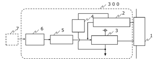
- FIG. 1 is a circuit diagram of a gate drive circuit according to Embodiment 1 of the present disclosure
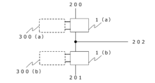
- FIG. BRIEF DESCRIPTION OF THE DRAWINGS It is a figure which shows the example of a partial structure of the power converter device which concerns on Embodiment 1 of this indication.
- 1 is a block diagram of a gate drive circuit according to Embodiment 1 of the present disclosure
- FIG. 1 is a diagram illustrating a configuration example of a buffer circuit according to a first embodiment of the present disclosure
- FIG. FIG. 10 is a diagram showing the results of a simulation study for comparing the gate drive circuit according to the first embodiment of the present disclosure and a conventional example
- FIG. 4 is a block diagram of a gate drive circuit according to Embodiment 2 of the present disclosure
- FIG. 10 is a diagram showing a gate drive circuit according to Embodiment 3 of the present disclosure
- FIG. 1 is a circuit diagram of a gate drive circuit according to Embodiment 1.
- FIG. FIG. 2 is a diagram showing a configuration example of a part of the gate drive circuit of the power converter.
- the power converter according to the first embodiment includes a semiconductor switching element 1 (hereinafter also referred to as a semiconductor SW element 1), and for example, converts externally input voltage, current, and power into desired voltage, current, and power. , a DCDC converter, an ACDC converter, a DCAC inverter, and an ACAC inverter.
- a semiconductor SW element 1 included in the power converter is driven by the gate drive circuit 300 shown in FIG.
- the gate drive circuit 300 includes a voltage feedback section 2, a gate drive section 3, a discharge section 4, a first current limiting element 5, and an insulation communication section 6, as shown in FIG. Then, the gate drive circuit 300 drives the semiconductor SW element 1 connected to the gate drive circuit 300 based on a command from the upper logic unit 7 .
- the power conversion device includes one or more gate drive circuits 300 .
- FIG. 2 shows an example in which two gate drive circuits 300 and two semiconductor SW elements 1 are included. b). Also, one gate drive circuit is shown as 300(a), and a configuration including another gate drive circuit is shown as 300(b).
- the gate drive circuit 300(a) is connected to the gate terminal and the collector (or drain) terminal of the semiconductor SW element 1(a), and the gate drive circuit 300(b) is connected to the semiconductor SW element 1(b).
- the emitter (or source) terminal of the semiconductor SW element 1 (a) and the collector (or drain) terminal of the semiconductor SW element 1 are connected.
- the collector (or drain) terminal of the semiconductor SW element 1(a) is connected to the positive side 200 of the power supply, and the emitter (or source) terminal of the semiconductor SW element 1(b) is connected to the negative side 201 of the power supply.
- a connection point between the semiconductor SW element 1(a) and the semiconductor SW element 1(b) serves as the output terminal 202 .
- the semiconductor SW elements 1(a) and 1(b) are alternately on/off-controlled by the gate drive circuits 300(a) and 300(b) to perform the power conversion operation. Desired electric power can be taken out.
- FIG. 3 shows a block diagram of the gate drive circuit according to the first embodiment.
- a MOSFET Metal Oxide Semiconductor Field Effect Transistor
- a SiC MOSFET or a Si MOSFET can be applied.
- the active clamp technology which is effective in reducing both switching loss and surge voltage at turn-off, has a stronger effect in SiC, which is capable of high-speed switching operation than Si.
- an IGBT (Insulated Gate Bipolar Transistor) module or a GaN-HEMT (Gallium nitride-High Mobility Transistor) in which diodes are connected in anti-parallel may be used.
- the anti-parallel diode a diode built in the MOSFET may be used, or a separate diode may be provided externally.
- the semiconductor SW element 1 will be described as an example of a MOSFET having an antiparallel diode between the source and the drain.
- the voltage feedback section 2 is connected to the drain side of the semiconductor SW element 1 .
- the voltage feedback unit 2 can detect the voltage of the high-potential main terminal on the drain side of the semiconductor SW element 1 .
- the voltage feedback section 2 is configured to feed back to the input side of the gate driving section 3 the voltage rise of the high-potential-side main terminal that occurs when the semiconductor SW element 1 is turned off. Thereby, a function (active clamp) of suppressing a surge voltage by increasing the gate voltage can be realized.
- the voltage feedback unit 2 includes a high withstand voltage capacitor 9 , a first reverse blocking diode 8 , and a second current limiting element 10 .
- Capacitor 9 transfers energy from the drain terminal of semiconductor SW element 1 . That is, capacitive coupling is made from the drain terminal of the semiconductor SW element 1 by the capacitor 9 .
- the anode of the first reverse blocking diode 8 is connected to the drain side of the semiconductor SW element 1, and the cathode of the first reverse blocking diode 8 is connected to the gate driver 3 side. This makes it possible to prevent backflow at turn-on.
- the second current limiting element 10 is a current limiting resistor. Specifically, the second current limiting element 10 is for adjusting the amount of feedback current to the gate signal necessary for active clamping. The resistance value of the second current limiting element 10 is adjusted by the capacitance of the capacitor 9 , the impedance of the first current limiting element 5 , the configuration of the gate driving section 3 and the capacitive characteristics of the semiconductor SW element 1 . Therefore, although the second current limiting element 10 is provided in the first embodiment, it may be omitted depending on the circuit design. Also, a constant voltage diode may be used instead of the capacitor 9 .
- the anode of the constant voltage diode is connected to the gate driver 3 side, and the cathode is connected to the drain side of the semiconductor SW element 1 .
- This has the effect of masking the active clamp operation until the surge voltage reaches a certain voltage. That is, by disabling the active clamp operation until the surge voltage reaches a certain voltage, high-speed switching can be realized, and a loss reduction effect can be obtained.
- the same effect can be obtained even if the connection order of the capacitor 9, the first reverse blocking diode 8, the second current limiting element 10, and the zener diode is changed. Also, some parts of the second current limiting element 10 can be eliminated.
- the voltage feedback section 2 may be connected to the output side of the gate driving section 3.
- the active clamping operation is performed by voltage feedback corresponding to a small current compared to the case where the voltage feedback section 2 is connected to the output side of the gate driving section 3. can be realized, the circuit scale of the voltage feedback section 2 can be reduced.
- the output of the gate driving section 3 is a large current compared to the case where the voltage feedback section 2 is connected to the input side of the gate driving section 3. Therefore, it does not respond to small noise currents and has good malfunction tolerance.
- FIG. 4A shows a one-stage push-pull (totem pole) circuit realized by combining an NPN transistor and a PNP transistor.
- FIG. 4B shows a multi-stage push-pull (totem pole) circuit in which two or more stages of one-stage push-pull (totem pole) circuits are arranged in series.
- FIG. 4A shows a one-stage push-pull (totem pole) circuit realized by combining an NPN transistor and a PNP transistor.
- FIG. 4B shows a multi-stage push-pull (totem pole) circuit in which two or more stages of one-stage push-pull (totem pole) circuits are arranged in series.
- a pre-driver is a drive circuit for driving a buffer circuit, and the pre-driver shown in FIG. It shows what you can do.
- the multi-stage push-pull circuit shown in FIG. 4(b) can obtain a stronger buffer capability than the one-stage configuration by connecting multiple stages in FIG. 4(a) in series. 4A and 4B, when the semiconductor SW element 1 is turned off, the collector voltage of the semiconductor SW element 1 rises. current flows to pull up the gate driver input signal S1. Therefore, the gate voltage of the semiconductor SW element 1 also rises, and the active clamp operation can be realized.
- the composite buffer circuit in FIG. 4(c) is a circuit comprising a buffer circuit composed of MOSFETs and a bipolar transistor in parallel with the source-side MOSFET of the buffer circuit.
- the threshold voltage of the MOSFET eg ⁇ 2.5V
- the threshold voltage of the bipolar transistor ⁇ 0.7V
- the first current limiting element 5 limits the circuit current in the insulating communication unit 6, and sets the input signal of the gate driving unit 3 to a value different from the output signal of the insulating communication unit 6 by the feedback signal from the voltage feedback unit 2. It is an element for The resistance value is adjusted by the capacity of capacitor 9 and the impedance of second current limiting element 10 , the configuration of gate driving section 3 and the capacitance characteristics of semiconductor SW element 1 .
- the isolation communication unit 6 is an isolator IC containing a photocoupler, a pulse transformer, etc. that generates an ON/OFF command signal while maintaining insulation from the upper logic unit 7 based on a signal sent from the upper logic unit 7 such as a microcomputer. consists of
- the discharge section 4 is arranged between the connection point between the capacitor 9 of the voltage feedback section 2 and the first reverse blocking diode 8 and the power supply potential applied to the control terminal when the semiconductor SW element 1 is turned off, for example.
- the discharge section 4 includes a second reverse blocking diode 11 and an inrush current suppressing element 12 .
- the second reverse blocking diode 11 has an anode connected to the negative potential side of the gate power supply, a cathode connected to the capacitor 9 side, and an inrush current suppressing element 12 connected either before or after it.
- the discharge time constant CR corresponding to the resistance value R of the current suppressing element 12 and the capacitance C of the capacitor 9
- the power supply applied to the control terminal when the semiconductor SW element 1 is turned off is indicated by the one-dot chain line in FIG. is discharged through a path flowing from the potential of , through the discharge portion 4 to the drain terminal of the semiconductor SW element 1 .
- the inrush current suppressing element 12 of the discharge section 4 is composed of a capacitor 9 and a resistor according to the specifications of the bus voltage in order to suppress the inrush current at the time of turn-on. Since it is a design element, it does not necessarily have to be provided. Further, if a path for discharging the electric charge charged in the capacitor 9 of the voltage feedback section 2 is secured, the effects of the first embodiment can be obtained. It can also be a place where a full loop of the discharge path can be obtained instead of the negative potential of the power supply. Furthermore, one end of the connection destination of the discharge section 4 may not be the connection point between the capacitor 9 of the voltage feedback section 2 and the first reverse blocking diode 8 as described above. It may be connected to the voltage feedback section 2 from the contact to the gate drive section 3 .
- FIG. 5 is a diagram showing the results of a simulation study conducted with and without the discharge section 4 based on the circuit block diagram of FIG.
- FIG. 5(a) shows the analyzed waveform without the discharge section 4
- FIG. 5(b) shows the analyzed waveform with the discharge section 4 of the first embodiment.
- the bus voltage at turn-on is about 600V, and the current is about 1000A.
- FIG. 5(a) shows the voltage applied to the first reverse blocking diode 8 of the voltage feedback section 2.
- FIG. 5B shows waveforms of the voltage applied to the first reverse blocking diode 8 of the voltage feedback section 2 and the discharge current flowing through the rush current suppressing element 12 added to the discharge section 4 .
- 5A and 5B waveforms of the gate-emitter voltage Vge, the collector-emitter voltage Vce, and the collector current Ic of the semiconductor SW element 1 driven by the gate drive unit 3 are shown in the lower part of each of FIGS. is shown.
- the voltage applied to the first reverse blocking diode 8 after turn-on is constant at about -600 V, which is the opposite polarity to the voltage of the capacitor 9.
- the discharge section 4 shown in FIG. 5B the voltage momentarily drops to -12V during discharge, but after discharge, the voltage drops by Vf from the voltage applied during OFF and stabilizes. This is because, as described above, in the gate drive circuit 300 according to the first embodiment, when the semiconductor SW element 1 is turned off, the electric charge charged in the capacitor 9 of the voltage feedback section 2 is made to flow to enable discharge. This is because it is secured.
- the discharge unit 4 can discharge the electric charge charged in the capacitor 9 of the voltage feedback unit 2 through the discharge path when the semiconductor SW element 1 is turned off to the drain terminal when the semiconductor SW element 1 is turned on. As a result, it is possible to prevent the voltage drop of the gate driving section 3 at the time of turn-on without using a high withstand voltage semiconductor component for the voltage feedback section 2 .
- Non-Patent Document 1 in which the information on the collector voltage of the IGBT is fed back to the input side of the gate driving section to improve the response, especially when the IGBT is turned on, the parasitic capacitance of the diode There is a problem that a voltage drop occurs in the resistance Rin on the buffer input side due to the flow of a very small mutated current, the gate voltage decreases, and the turn-on loss increases. Alternatively, a malfunction may occur in which the gate voltage oscillates at turn-on. The mechanism by which this malfunction occurs will be described below with reference to FIG. When the gate is turned on ((a) in FIG.
- Vce decreases (b), so that a capacitive displacement current flows in the reverse direction through the reverse blocking diode (c) through Rin, and the gate driving part by Rin
- the input voltage drops (d) and the gate turns off (e).
- Vce rises again (f), and current flows through Rin in the forward direction of the reverse-blocking diode (g). It rises to the voltage on the positive side of the power supply (h).
- the gate since the gate is turned on, the operations described in (i), (a) to (f) are repeated, and the gate is repeatedly turned on and off.
- a discharge path is secured for discharging the charge charged in the capacitor 9 of the voltage feedback unit 2 when the semiconductor SW element 1 is turned off. Therefore, it becomes unnecessary to use a high withstand voltage component in the voltage feedback section 2 .
- the discharge path constitutes a path from the contact of the capacitance on the side of the gate driving section to the gate driving section. In other words, the discharge section 4 secures a path that does not pass through the first current limiting element 5 .
- the voltage feedback unit 2 when the voltage feedback unit 2 is turned on, the current that discharges the charge charged in the parasitic capacitance of the first reverse blocking diode 8 of the voltage feedback unit 2 flows through the gate driving unit 3, causing a voltage drop in the first current limiting element 5, resulting in a malfunction. can be prevented.
- the gate drive circuit 300 shown in the first embodiment includes the gate drive section 3 that applies a gate drive voltage to the control terminal of the semiconductor SW element 1 to drive the semiconductor SW element 1, and the high potential of the semiconductor SW element 1. and a voltage feedback section 2 connected to the main terminal for feeding back to the gate driving section 3 the rise in the voltage of the high-potential main terminal that occurs when the semiconductor SW element 1 is turned off.
- a discharge section 4 that forms a path for discharging the capacitance included in the voltage feedback section 2 when the semiconductor SW element 1 is turned on. As a result, the charge charged in the capacitor 9 of the voltage feedback section 2 can be caused to flow and be discharged.
- the power conversion apparatus shown in Embodiment 1 is configured to include one or more gate drive circuits 300 and one or more semiconductor SW elements 1 . As a result, it is possible to convert the externally input voltage, current, and power into the desired voltage, current, and power while preventing the voltage drop of the gate driving section 3 at the time of turn-on without using a high-voltage semiconductor component. It becomes possible.
- FIG. 7 and 8 are diagrams showing gate drive circuit 400 according to the second embodiment.
- a power conversion device is configured including a gate drive circuit 400.
- the gate drive circuit 400 includes a voltage feedback section 2, a gate drive section 3, a discharge section 4, a first current limiting element 5, an insulation A communication unit 6 is included. Since this configuration is the same as that of the first embodiment, detailed descriptions of the same components will be omitted, and only the differences from the first embodiment will be described below.
- the second embodiment is obtained by changing the configurations of the voltage feedback section 2 and the discharge section 4 of the first embodiment. Specifically, as shown in FIG. 8, the voltage feedback section 2 is configured without the first reverse blocking diode 8 for preventing backflow. Also, the connection destination of the discharge portion 4 is different from that in the first embodiment.
- the discharge section 4 in Embodiment 2 is composed of a second reverse blocking diode 11 and an inrush current suppressing element 12 .
- the discharge section 4 is arranged in parallel with the first current limiting element 5 .
- the second reverse blocking diode 11 has an anode connected to the output side of the insulating communication section 6 and a cathode connected to the input sides of the voltage feedback section 2 and the gate drive section 3 .
- the inrush current suppressing element 12 may be connected either before or after the second reverse blocking diode 11, and FIG. Also, the impedance of the rush current suppressing element 12 is set smaller than the impedance of the first current limiting element 5 .
- the discharge section 4 By providing the discharge section 4 in this way, the electric charge of the capacitor 9 charged in the direction of the gate signal from the collector terminal when the semiconductor SW element 1 is turned off is transferred to the insulating communication section when it is turned on, as shown by the dashed-dotted line in FIG. 6 flows to the collector terminal of the semiconductor SW element 1 via the discharge section 4, and can be discharged.
- the discharge section 4 By providing the discharge section 4, the above-mentioned path is secured, and voltage drop of the gate drive section 3 at turn-on can be prevented without providing a high-voltage semiconductor component as a component of the voltage feedback section 2.
- the discharge section 4 is arranged in parallel with the first current limiting element 5 so that the main discharge path does not pass through the first current limiting element 5 . Therefore, it is possible to suppress the voltage drop due to the first current limiting element 5 and suppress the malfunction.
- the inrush current suppressing element 12 of the discharge section 4 is composed of a resistor in accordance with the specifications of the capacitor 9 and the bus voltage in order to suppress the inrush current at the time of turn-on. It is not necessary and can be omitted.
- FIG. 9 shows a gate drive circuit 500 according to the third embodiment.
- a power conversion device is configured by including a gate drive circuit 500.
- the gate drive circuit 500 includes a voltage feedback section 2, a gate drive section 3, a discharge section 4, a first current limiting element 5, an insulation A communication unit 6 is included. Since this configuration is the same as that of the first and second embodiments, detailed description of similar components will be omitted, and only the differences from the first and second embodiments will be described below.
- the discharge unit 4 has the same configuration as that of the second embodiment, the configuration of the first embodiment or the combination of the configurations of the discharge units 4 of the first and second embodiments is applied as appropriate. It is possible to
- Embodiments 1 and 2 described the invention relating to a gate drive circuit having an active clamping function, but Embodiment 3 is configured to optimize the active clamping operation with the switching switch 13. .
- the switching switch 13 and the second current limiting element 10(b) are connected in series to the low voltage side of the capacitor 9 of the voltage feedback section 2. in parallel with a second current limiting device 10(a).
- the switching switch 13 is configured using a switching semiconductor switching element 14 such as a MOSFET (hereinafter also referred to as a switching semiconductor SW element 14).
- the change-over switch 13 can control the change-over switch 13 by predicting the surge voltage when the semiconductor SW element 1 is turned on based on the information on the current or voltage flowing through the main circuit.
- the second current limiting element 10(b) is set to a sufficiently small value
- the second current limiting element 10(a) is set to a value sufficiently larger than 10(b)
- the surge voltage exceeds the allowable voltage.
- the switching semiconductor SW element 14 is turned on and off, and the combined resistance value of the second current limiting element is set to a small value determined by the parallel circuit of 10(a) and 10(b). to strengthen the effect of the surge voltage reduction.
- the switching semiconductor SW element 14 is controlled to be turned off, and the combined resistance value of the second current limiting element is set to a sufficiently large value of 10(a), thereby providing an active clamping function. Weaken the effect of In other words, the switching switch 13 can be used to switch the feedback action between stronger and weaker.
- the second current limiting element 10(b) has a sufficiently small value.
- a parallel circuit configuration of the switching switch 13 may be used.
- the effectiveness of the active clamp can be greatly changed by turning the switching switch 13 on and off.
- the active clamp function is strengthened (effective )/miniaturization (disabling) can also be controlled.
- the active clamp function can be minimized (disabled) to suppress the increase in the gate voltage due to the active clamp, thereby reducing switching loss. It becomes possible.
- the third embodiment is also effective when there are conflicting demands on the active clamp function at the time of recovery and at the time of turn-off.
- the combined resistance value of the second current limiting element is set to a sufficiently large value to weaken the effect of the active clamp function and realize low loss, while recovery
- the combined resistance value of the second current limiting element is made small to enhance the effect of the active clamp function, thereby suppressing the recovery surge voltage.
Landscapes
- Engineering & Computer Science (AREA)
- Power Engineering (AREA)
- Power Conversion In General (AREA)
- Electronic Switches (AREA)
Priority Applications (5)
| Application Number | Priority Date | Filing Date | Title |
|---|---|---|---|
| JP2024502285A JP7720983B2 (ja) | 2022-02-22 | 2022-02-22 | ゲート駆動回路およびこれを用いた電力変換装置 |
| US18/836,379 US12525868B2 (en) | 2022-02-22 | 2022-02-22 | Gate drive circuit and power conversion device using same |
| DE112022006700.4T DE112022006700T5 (de) | 2022-02-22 | 2022-02-22 | Gate-Treiberschaltung und Energie-Umwandlungseinrichtung, die diese verwendet |
| PCT/JP2022/007362 WO2023162032A1 (ja) | 2022-02-22 | 2022-02-22 | ゲート駆動回路およびこれを用いた電力変換装置 |
| CN202280091907.6A CN118715701A (zh) | 2022-02-22 | 2022-02-22 | 栅极驱动电路以及使用该栅极驱动电路的电力变换装置 |
Applications Claiming Priority (1)
| Application Number | Priority Date | Filing Date | Title |
|---|---|---|---|
| PCT/JP2022/007362 WO2023162032A1 (ja) | 2022-02-22 | 2022-02-22 | ゲート駆動回路およびこれを用いた電力変換装置 |
Publications (1)
| Publication Number | Publication Date |
|---|---|
| WO2023162032A1 true WO2023162032A1 (ja) | 2023-08-31 |
Family
ID=87765189
Family Applications (1)
| Application Number | Title | Priority Date | Filing Date |
|---|---|---|---|
| PCT/JP2022/007362 Ceased WO2023162032A1 (ja) | 2022-02-22 | 2022-02-22 | ゲート駆動回路およびこれを用いた電力変換装置 |
Country Status (5)
| Country | Link |
|---|---|
| US (1) | US12525868B2 (https=) |
| JP (1) | JP7720983B2 (https=) |
| CN (1) | CN118715701A (https=) |
| DE (1) | DE112022006700T5 (https=) |
| WO (1) | WO2023162032A1 (https=) |
Citations (3)
| Publication number | Priority date | Publication date | Assignee | Title |
|---|---|---|---|---|
| JP2009131035A (ja) * | 2007-11-22 | 2009-06-11 | Toyota Motor Corp | スイッチング装置 |
| JP2018528607A (ja) * | 2015-08-07 | 2018-09-27 | デーン プルス シェーネ ゲーエムベーハ プルス ツェオー.カーゲー | 供給ネットワークから動作されるユニットをサージから保護するための回路アセンブリ |
| JP2019129565A (ja) * | 2018-01-23 | 2019-08-01 | 日産自動車株式会社 | 駆動装置 |
Family Cites Families (4)
| Publication number | Priority date | Publication date | Assignee | Title |
|---|---|---|---|---|
| JP3883925B2 (ja) * | 2002-07-30 | 2007-02-21 | 三菱電機株式会社 | 電力用半導体素子の駆動回路 |
| DE102007063721B4 (de) | 2006-03-22 | 2014-05-08 | Denso Corporation | Schaltkreis mit einem Transistor und einer Ansteuerschaltung zur Ansteuerung des Transistors |
| JP4971848B2 (ja) | 2006-03-22 | 2012-07-11 | 株式会社豊田中央研究所 | 低スイッチング損失、低ノイズを両立するパワーmos回路 |
| US9640972B2 (en) * | 2014-03-26 | 2017-05-02 | Infineon Technologies Ag | Controlled switch-off of a power switch |
-
2022
- 2022-02-22 JP JP2024502285A patent/JP7720983B2/ja active Active
- 2022-02-22 US US18/836,379 patent/US12525868B2/en active Active
- 2022-02-22 CN CN202280091907.6A patent/CN118715701A/zh active Pending
- 2022-02-22 DE DE112022006700.4T patent/DE112022006700T5/de active Pending
- 2022-02-22 WO PCT/JP2022/007362 patent/WO2023162032A1/ja not_active Ceased
Patent Citations (3)
| Publication number | Priority date | Publication date | Assignee | Title |
|---|---|---|---|---|
| JP2009131035A (ja) * | 2007-11-22 | 2009-06-11 | Toyota Motor Corp | スイッチング装置 |
| JP2018528607A (ja) * | 2015-08-07 | 2018-09-27 | デーン プルス シェーネ ゲーエムベーハ プルス ツェオー.カーゲー | 供給ネットワークから動作されるユニットをサージから保護するための回路アセンブリ |
| JP2019129565A (ja) * | 2018-01-23 | 2019-08-01 | 日産自動車株式会社 | 駆動装置 |
Also Published As
| Publication number | Publication date |
|---|---|
| JPWO2023162032A1 (https=) | 2023-08-31 |
| CN118715701A (zh) | 2024-09-27 |
| DE112022006700T5 (de) | 2024-12-05 |
| US12525868B2 (en) | 2026-01-13 |
| JP7720983B2 (ja) | 2025-08-08 |
| US20250141338A1 (en) | 2025-05-01 |
Similar Documents
| Publication | Publication Date | Title |
|---|---|---|
| US9793260B2 (en) | System and method for a switch having a normally-on transistor and a normally-off transistor | |
| KR101217357B1 (ko) | 전력용 반도체 소자의 구동 회로 | |
| US9954521B2 (en) | Gate drive circuit for semiconductor switching devices | |
| US7236041B2 (en) | Isolated gate driver circuit for power switching devices | |
| US20120235710A1 (en) | Circuit Arrangement with a MOSFET and an IGBT | |
| KR20110123169A (ko) | 스위칭 게이트 드라이브 | |
| CN113497610B (zh) | 可降低功率半导体传导损耗的栅极驱动电路 | |
| US20210242864A1 (en) | Switch circuit capable of overcurrent protection with small and simple circuit, and with simple operation, without affecting normal operation | |
| US20200036380A1 (en) | Driving device and switching device | |
| US8638134B2 (en) | Gate drive circuit and power semiconductor module | |
| JP2010130557A (ja) | ゲート駆動装置 | |
| US11799468B2 (en) | Semiconductor device and control system | |
| Bindra | Recent Advances in Gate Driver Integrated Circuits for Wide-Bandgap FETs: Manufacturers introduce gate drivers for squeezing the best performance out of WBG devices | |
| JP2020096444A (ja) | スイッチング回路 | |
| WO2023062745A1 (ja) | 電力用半導体素子の駆動回路、電力用半導体モジュール、および電力変換装置 | |
| CN210075194U (zh) | 可控硅驱动电路 | |
| JP7720983B2 (ja) | ゲート駆動回路およびこれを用いた電力変換装置 | |
| JPWO2023162032A5 (https=) | ||
| JP4253318B2 (ja) | スイッチング手段駆動回路、スイッチング手段の駆動方法、電源装置、及びスイッチング回路 | |
| JPH10209832A (ja) | 半導体スイッチ回路 | |
| CN115708301A (zh) | 驱动装置 | |
| JP6370524B1 (ja) | ゲート駆動回路 | |
| JP2000139071A (ja) | 電力変換装置のゲート駆動回路 | |
| CN111082788B (zh) | 栅极驱动装置及电子设备 | |
| US20230179199A1 (en) | Drive circuit |
Legal Events
| Date | Code | Title | Description |
|---|---|---|---|
| 121 | Ep: the epo has been informed by wipo that ep was designated in this application |
Ref document number: 22928563 Country of ref document: EP Kind code of ref document: A1 |
|
| ENP | Entry into the national phase |
Ref document number: 2024502285 Country of ref document: JP Kind code of ref document: A |
|
| WWE | Wipo information: entry into national phase |
Ref document number: 18836379 Country of ref document: US |
|
| WWE | Wipo information: entry into national phase |
Ref document number: 202280091907.6 Country of ref document: CN |
|
| WWE | Wipo information: entry into national phase |
Ref document number: 112022006700 Country of ref document: DE |
|
| 122 | Ep: pct application non-entry in european phase |
Ref document number: 22928563 Country of ref document: EP Kind code of ref document: A1 |
|
| WWP | Wipo information: published in national office |
Ref document number: 18836379 Country of ref document: US |
|
| WWG | Wipo information: grant in national office |
Ref document number: 18836379 Country of ref document: US |