WO2023162032A1 - Gate drive circuit and power conversion device using same - Google Patents
Gate drive circuit and power conversion device using same Download PDFInfo
- Publication number
- WO2023162032A1 WO2023162032A1 PCT/JP2022/007362 JP2022007362W WO2023162032A1 WO 2023162032 A1 WO2023162032 A1 WO 2023162032A1 JP 2022007362 W JP2022007362 W JP 2022007362W WO 2023162032 A1 WO2023162032 A1 WO 2023162032A1
- Authority
- WO
- WIPO (PCT)
- Prior art keywords
- gate drive
- voltage
- section
- switching element
- drive circuit
- Prior art date
Links
Images


Classifications
-
- H—ELECTRICITY
- H02—GENERATION; CONVERSION OR DISTRIBUTION OF ELECTRIC POWER
- H02M—APPARATUS FOR CONVERSION BETWEEN AC AND AC, BETWEEN AC AND DC, OR BETWEEN DC AND DC, AND FOR USE WITH MAINS OR SIMILAR POWER SUPPLY SYSTEMS; CONVERSION OF DC OR AC INPUT POWER INTO SURGE OUTPUT POWER; CONTROL OR REGULATION THEREOF
- H02M1/00—Details of apparatus for conversion
- H02M1/08—Circuits specially adapted for the generation of control voltages for semiconductor devices incorporated in static converters
Definitions
- the present disclosure relates to a gate drive circuit and a power converter using the same.
- Non-Patent Document 1 there is a configuration in which information on the collector voltage of the IGBT is fed back to the input side of the gate driving section as a means of achieving high responsiveness (for example, Non-Patent Document 1).
- Non-Patent Document 1 it was necessary to use high-voltage components in order to prevent gate voltage drop.
- a minute displacement current flows through the parasitic capacitance of the diode, causing a voltage drop across the resistance Rin on the buffer input side, lowering the gate voltage and increasing the turn-on loss.
- the present disclosure aims to provide a power conversion device that can prevent a voltage drop in the gate drive section during turn-on without using a high-voltage semiconductor component in the voltage feedback section. aim.
- a gate drive circuit unit is connected to a gate drive unit that applies a gate drive voltage to a control terminal of a semiconductor switching element to drive the semiconductor switching element, and a high-potential main terminal of the semiconductor switching element.
- a voltage feedback unit that feeds back the voltage of the high-potential main terminal generated at the time of turn-off of the semiconductor switching element to the gate drive unit, and discharges the charge contained in the voltage feedback unit to the high-potential main terminal side of the semiconductor switching element when the semiconductor switching element is turned on. and a discharge section forming a path.
- the power conversion device includes a gate drive circuit and a semiconductor switching element, and converts externally input power into desired power by turning on/off the semiconductor switching element.
- the gate drive circuit of the present disclosure it is possible to prevent a voltage drop in the gate drive section during turn-on without using a high-voltage semiconductor component in the voltage feedback section.
- FIG. 1 is a circuit diagram of a gate drive circuit according to Embodiment 1 of the present disclosure
- FIG. BRIEF DESCRIPTION OF THE DRAWINGS It is a figure which shows the example of a partial structure of the power converter device which concerns on Embodiment 1 of this indication.
- 1 is a block diagram of a gate drive circuit according to Embodiment 1 of the present disclosure
- FIG. 1 is a diagram illustrating a configuration example of a buffer circuit according to a first embodiment of the present disclosure
- FIG. FIG. 10 is a diagram showing the results of a simulation study for comparing the gate drive circuit according to the first embodiment of the present disclosure and a conventional example
- FIG. 4 is a block diagram of a gate drive circuit according to Embodiment 2 of the present disclosure
- FIG. 10 is a diagram showing a gate drive circuit according to Embodiment 3 of the present disclosure
- FIG. 1 is a circuit diagram of a gate drive circuit according to Embodiment 1.
- FIG. FIG. 2 is a diagram showing a configuration example of a part of the gate drive circuit of the power converter.
- the power converter according to the first embodiment includes a semiconductor switching element 1 (hereinafter also referred to as a semiconductor SW element 1), and for example, converts externally input voltage, current, and power into desired voltage, current, and power. , a DCDC converter, an ACDC converter, a DCAC inverter, and an ACAC inverter.
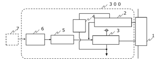
- a semiconductor SW element 1 included in the power converter is driven by the gate drive circuit 300 shown in FIG.
- the gate drive circuit 300 includes a voltage feedback section 2, a gate drive section 3, a discharge section 4, a first current limiting element 5, and an insulation communication section 6, as shown in FIG. Then, the gate drive circuit 300 drives the semiconductor SW element 1 connected to the gate drive circuit 300 based on a command from the upper logic unit 7 .
- the power conversion device includes one or more gate drive circuits 300 .
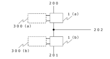
- FIG. 2 shows an example in which two gate drive circuits 300 and two semiconductor SW elements 1 are included. b). Also, one gate drive circuit is shown as 300(a), and a configuration including another gate drive circuit is shown as 300(b).
- the gate drive circuit 300(a) is connected to the gate terminal and the collector (or drain) terminal of the semiconductor SW element 1(a), and the gate drive circuit 300(b) is connected to the semiconductor SW element 1(b).
- the emitter (or source) terminal of the semiconductor SW element 1 (a) and the collector (or drain) terminal of the semiconductor SW element 1 are connected.
- the collector (or drain) terminal of the semiconductor SW element 1(a) is connected to the positive side 200 of the power supply, and the emitter (or source) terminal of the semiconductor SW element 1(b) is connected to the negative side 201 of the power supply.
- a connection point between the semiconductor SW element 1(a) and the semiconductor SW element 1(b) serves as the output terminal 202 .
- the semiconductor SW elements 1(a) and 1(b) are alternately on/off-controlled by the gate drive circuits 300(a) and 300(b) to perform the power conversion operation. Desired electric power can be taken out.
- FIG. 3 shows a block diagram of the gate drive circuit according to the first embodiment.
- a MOSFET Metal Oxide Semiconductor Field Effect Transistor
- a SiC MOSFET or a Si MOSFET can be applied.
- the active clamp technology which is effective in reducing both switching loss and surge voltage at turn-off, has a stronger effect in SiC, which is capable of high-speed switching operation than Si.
- an IGBT (Insulated Gate Bipolar Transistor) module or a GaN-HEMT (Gallium nitride-High Mobility Transistor) in which diodes are connected in anti-parallel may be used.
- the anti-parallel diode a diode built in the MOSFET may be used, or a separate diode may be provided externally.
- the semiconductor SW element 1 will be described as an example of a MOSFET having an antiparallel diode between the source and the drain.
- the voltage feedback section 2 is connected to the drain side of the semiconductor SW element 1 .
- the voltage feedback unit 2 can detect the voltage of the high-potential main terminal on the drain side of the semiconductor SW element 1 .
- the voltage feedback section 2 is configured to feed back to the input side of the gate driving section 3 the voltage rise of the high-potential-side main terminal that occurs when the semiconductor SW element 1 is turned off. Thereby, a function (active clamp) of suppressing a surge voltage by increasing the gate voltage can be realized.
- the voltage feedback unit 2 includes a high withstand voltage capacitor 9 , a first reverse blocking diode 8 , and a second current limiting element 10 .
- Capacitor 9 transfers energy from the drain terminal of semiconductor SW element 1 . That is, capacitive coupling is made from the drain terminal of the semiconductor SW element 1 by the capacitor 9 .
- the anode of the first reverse blocking diode 8 is connected to the drain side of the semiconductor SW element 1, and the cathode of the first reverse blocking diode 8 is connected to the gate driver 3 side. This makes it possible to prevent backflow at turn-on.
- the second current limiting element 10 is a current limiting resistor. Specifically, the second current limiting element 10 is for adjusting the amount of feedback current to the gate signal necessary for active clamping. The resistance value of the second current limiting element 10 is adjusted by the capacitance of the capacitor 9 , the impedance of the first current limiting element 5 , the configuration of the gate driving section 3 and the capacitive characteristics of the semiconductor SW element 1 . Therefore, although the second current limiting element 10 is provided in the first embodiment, it may be omitted depending on the circuit design. Also, a constant voltage diode may be used instead of the capacitor 9 .
- the anode of the constant voltage diode is connected to the gate driver 3 side, and the cathode is connected to the drain side of the semiconductor SW element 1 .
- This has the effect of masking the active clamp operation until the surge voltage reaches a certain voltage. That is, by disabling the active clamp operation until the surge voltage reaches a certain voltage, high-speed switching can be realized, and a loss reduction effect can be obtained.
- the same effect can be obtained even if the connection order of the capacitor 9, the first reverse blocking diode 8, the second current limiting element 10, and the zener diode is changed. Also, some parts of the second current limiting element 10 can be eliminated.
- the voltage feedback section 2 may be connected to the output side of the gate driving section 3.
- the active clamping operation is performed by voltage feedback corresponding to a small current compared to the case where the voltage feedback section 2 is connected to the output side of the gate driving section 3. can be realized, the circuit scale of the voltage feedback section 2 can be reduced.
- the output of the gate driving section 3 is a large current compared to the case where the voltage feedback section 2 is connected to the input side of the gate driving section 3. Therefore, it does not respond to small noise currents and has good malfunction tolerance.
- FIG. 4A shows a one-stage push-pull (totem pole) circuit realized by combining an NPN transistor and a PNP transistor.
- FIG. 4B shows a multi-stage push-pull (totem pole) circuit in which two or more stages of one-stage push-pull (totem pole) circuits are arranged in series.
- FIG. 4A shows a one-stage push-pull (totem pole) circuit realized by combining an NPN transistor and a PNP transistor.
- FIG. 4B shows a multi-stage push-pull (totem pole) circuit in which two or more stages of one-stage push-pull (totem pole) circuits are arranged in series.
- a pre-driver is a drive circuit for driving a buffer circuit, and the pre-driver shown in FIG. It shows what you can do.
- the multi-stage push-pull circuit shown in FIG. 4(b) can obtain a stronger buffer capability than the one-stage configuration by connecting multiple stages in FIG. 4(a) in series. 4A and 4B, when the semiconductor SW element 1 is turned off, the collector voltage of the semiconductor SW element 1 rises. current flows to pull up the gate driver input signal S1. Therefore, the gate voltage of the semiconductor SW element 1 also rises, and the active clamp operation can be realized.
- the composite buffer circuit in FIG. 4(c) is a circuit comprising a buffer circuit composed of MOSFETs and a bipolar transistor in parallel with the source-side MOSFET of the buffer circuit.
- the threshold voltage of the MOSFET eg ⁇ 2.5V
- the threshold voltage of the bipolar transistor ⁇ 0.7V
- the first current limiting element 5 limits the circuit current in the insulating communication unit 6, and sets the input signal of the gate driving unit 3 to a value different from the output signal of the insulating communication unit 6 by the feedback signal from the voltage feedback unit 2. It is an element for The resistance value is adjusted by the capacity of capacitor 9 and the impedance of second current limiting element 10 , the configuration of gate driving section 3 and the capacitance characteristics of semiconductor SW element 1 .
- the isolation communication unit 6 is an isolator IC containing a photocoupler, a pulse transformer, etc. that generates an ON/OFF command signal while maintaining insulation from the upper logic unit 7 based on a signal sent from the upper logic unit 7 such as a microcomputer. consists of
- the discharge section 4 is arranged between the connection point between the capacitor 9 of the voltage feedback section 2 and the first reverse blocking diode 8 and the power supply potential applied to the control terminal when the semiconductor SW element 1 is turned off, for example.
- the discharge section 4 includes a second reverse blocking diode 11 and an inrush current suppressing element 12 .
- the second reverse blocking diode 11 has an anode connected to the negative potential side of the gate power supply, a cathode connected to the capacitor 9 side, and an inrush current suppressing element 12 connected either before or after it.
- the discharge time constant CR corresponding to the resistance value R of the current suppressing element 12 and the capacitance C of the capacitor 9
- the power supply applied to the control terminal when the semiconductor SW element 1 is turned off is indicated by the one-dot chain line in FIG. is discharged through a path flowing from the potential of , through the discharge portion 4 to the drain terminal of the semiconductor SW element 1 .
- the inrush current suppressing element 12 of the discharge section 4 is composed of a capacitor 9 and a resistor according to the specifications of the bus voltage in order to suppress the inrush current at the time of turn-on. Since it is a design element, it does not necessarily have to be provided. Further, if a path for discharging the electric charge charged in the capacitor 9 of the voltage feedback section 2 is secured, the effects of the first embodiment can be obtained. It can also be a place where a full loop of the discharge path can be obtained instead of the negative potential of the power supply. Furthermore, one end of the connection destination of the discharge section 4 may not be the connection point between the capacitor 9 of the voltage feedback section 2 and the first reverse blocking diode 8 as described above. It may be connected to the voltage feedback section 2 from the contact to the gate drive section 3 .
- FIG. 5 is a diagram showing the results of a simulation study conducted with and without the discharge section 4 based on the circuit block diagram of FIG.
- FIG. 5(a) shows the analyzed waveform without the discharge section 4
- FIG. 5(b) shows the analyzed waveform with the discharge section 4 of the first embodiment.
- the bus voltage at turn-on is about 600V, and the current is about 1000A.
- FIG. 5(a) shows the voltage applied to the first reverse blocking diode 8 of the voltage feedback section 2.
- FIG. 5B shows waveforms of the voltage applied to the first reverse blocking diode 8 of the voltage feedback section 2 and the discharge current flowing through the rush current suppressing element 12 added to the discharge section 4 .
- 5A and 5B waveforms of the gate-emitter voltage Vge, the collector-emitter voltage Vce, and the collector current Ic of the semiconductor SW element 1 driven by the gate drive unit 3 are shown in the lower part of each of FIGS. is shown.
- the voltage applied to the first reverse blocking diode 8 after turn-on is constant at about -600 V, which is the opposite polarity to the voltage of the capacitor 9.
- the discharge section 4 shown in FIG. 5B the voltage momentarily drops to -12V during discharge, but after discharge, the voltage drops by Vf from the voltage applied during OFF and stabilizes. This is because, as described above, in the gate drive circuit 300 according to the first embodiment, when the semiconductor SW element 1 is turned off, the electric charge charged in the capacitor 9 of the voltage feedback section 2 is made to flow to enable discharge. This is because it is secured.
- the discharge unit 4 can discharge the electric charge charged in the capacitor 9 of the voltage feedback unit 2 through the discharge path when the semiconductor SW element 1 is turned off to the drain terminal when the semiconductor SW element 1 is turned on. As a result, it is possible to prevent the voltage drop of the gate driving section 3 at the time of turn-on without using a high withstand voltage semiconductor component for the voltage feedback section 2 .
- Non-Patent Document 1 in which the information on the collector voltage of the IGBT is fed back to the input side of the gate driving section to improve the response, especially when the IGBT is turned on, the parasitic capacitance of the diode There is a problem that a voltage drop occurs in the resistance Rin on the buffer input side due to the flow of a very small mutated current, the gate voltage decreases, and the turn-on loss increases. Alternatively, a malfunction may occur in which the gate voltage oscillates at turn-on. The mechanism by which this malfunction occurs will be described below with reference to FIG. When the gate is turned on ((a) in FIG.
- Vce decreases (b), so that a capacitive displacement current flows in the reverse direction through the reverse blocking diode (c) through Rin, and the gate driving part by Rin
- the input voltage drops (d) and the gate turns off (e).
- Vce rises again (f), and current flows through Rin in the forward direction of the reverse-blocking diode (g). It rises to the voltage on the positive side of the power supply (h).
- the gate since the gate is turned on, the operations described in (i), (a) to (f) are repeated, and the gate is repeatedly turned on and off.
- a discharge path is secured for discharging the charge charged in the capacitor 9 of the voltage feedback unit 2 when the semiconductor SW element 1 is turned off. Therefore, it becomes unnecessary to use a high withstand voltage component in the voltage feedback section 2 .
- the discharge path constitutes a path from the contact of the capacitance on the side of the gate driving section to the gate driving section. In other words, the discharge section 4 secures a path that does not pass through the first current limiting element 5 .
- the voltage feedback unit 2 when the voltage feedback unit 2 is turned on, the current that discharges the charge charged in the parasitic capacitance of the first reverse blocking diode 8 of the voltage feedback unit 2 flows through the gate driving unit 3, causing a voltage drop in the first current limiting element 5, resulting in a malfunction. can be prevented.
- the gate drive circuit 300 shown in the first embodiment includes the gate drive section 3 that applies a gate drive voltage to the control terminal of the semiconductor SW element 1 to drive the semiconductor SW element 1, and the high potential of the semiconductor SW element 1. and a voltage feedback section 2 connected to the main terminal for feeding back to the gate driving section 3 the rise in the voltage of the high-potential main terminal that occurs when the semiconductor SW element 1 is turned off.
- a discharge section 4 that forms a path for discharging the capacitance included in the voltage feedback section 2 when the semiconductor SW element 1 is turned on. As a result, the charge charged in the capacitor 9 of the voltage feedback section 2 can be caused to flow and be discharged.
- the power conversion apparatus shown in Embodiment 1 is configured to include one or more gate drive circuits 300 and one or more semiconductor SW elements 1 . As a result, it is possible to convert the externally input voltage, current, and power into the desired voltage, current, and power while preventing the voltage drop of the gate driving section 3 at the time of turn-on without using a high-voltage semiconductor component. It becomes possible.
- FIG. 7 and 8 are diagrams showing gate drive circuit 400 according to the second embodiment.
- a power conversion device is configured including a gate drive circuit 400.
- the gate drive circuit 400 includes a voltage feedback section 2, a gate drive section 3, a discharge section 4, a first current limiting element 5, an insulation A communication unit 6 is included. Since this configuration is the same as that of the first embodiment, detailed descriptions of the same components will be omitted, and only the differences from the first embodiment will be described below.
- the second embodiment is obtained by changing the configurations of the voltage feedback section 2 and the discharge section 4 of the first embodiment. Specifically, as shown in FIG. 8, the voltage feedback section 2 is configured without the first reverse blocking diode 8 for preventing backflow. Also, the connection destination of the discharge portion 4 is different from that in the first embodiment.
- the discharge section 4 in Embodiment 2 is composed of a second reverse blocking diode 11 and an inrush current suppressing element 12 .
- the discharge section 4 is arranged in parallel with the first current limiting element 5 .
- the second reverse blocking diode 11 has an anode connected to the output side of the insulating communication section 6 and a cathode connected to the input sides of the voltage feedback section 2 and the gate drive section 3 .
- the inrush current suppressing element 12 may be connected either before or after the second reverse blocking diode 11, and FIG. Also, the impedance of the rush current suppressing element 12 is set smaller than the impedance of the first current limiting element 5 .
- the discharge section 4 By providing the discharge section 4 in this way, the electric charge of the capacitor 9 charged in the direction of the gate signal from the collector terminal when the semiconductor SW element 1 is turned off is transferred to the insulating communication section when it is turned on, as shown by the dashed-dotted line in FIG. 6 flows to the collector terminal of the semiconductor SW element 1 via the discharge section 4, and can be discharged.
- the discharge section 4 By providing the discharge section 4, the above-mentioned path is secured, and voltage drop of the gate drive section 3 at turn-on can be prevented without providing a high-voltage semiconductor component as a component of the voltage feedback section 2.
- the discharge section 4 is arranged in parallel with the first current limiting element 5 so that the main discharge path does not pass through the first current limiting element 5 . Therefore, it is possible to suppress the voltage drop due to the first current limiting element 5 and suppress the malfunction.
- the inrush current suppressing element 12 of the discharge section 4 is composed of a resistor in accordance with the specifications of the capacitor 9 and the bus voltage in order to suppress the inrush current at the time of turn-on. It is not necessary and can be omitted.
- FIG. 9 shows a gate drive circuit 500 according to the third embodiment.
- a power conversion device is configured by including a gate drive circuit 500.
- the gate drive circuit 500 includes a voltage feedback section 2, a gate drive section 3, a discharge section 4, a first current limiting element 5, an insulation A communication unit 6 is included. Since this configuration is the same as that of the first and second embodiments, detailed description of similar components will be omitted, and only the differences from the first and second embodiments will be described below.
- the discharge unit 4 has the same configuration as that of the second embodiment, the configuration of the first embodiment or the combination of the configurations of the discharge units 4 of the first and second embodiments is applied as appropriate. It is possible to
- Embodiments 1 and 2 described the invention relating to a gate drive circuit having an active clamping function, but Embodiment 3 is configured to optimize the active clamping operation with the switching switch 13. .
- the switching switch 13 and the second current limiting element 10(b) are connected in series to the low voltage side of the capacitor 9 of the voltage feedback section 2. in parallel with a second current limiting device 10(a).
- the switching switch 13 is configured using a switching semiconductor switching element 14 such as a MOSFET (hereinafter also referred to as a switching semiconductor SW element 14).
- the change-over switch 13 can control the change-over switch 13 by predicting the surge voltage when the semiconductor SW element 1 is turned on based on the information on the current or voltage flowing through the main circuit.
- the second current limiting element 10(b) is set to a sufficiently small value
- the second current limiting element 10(a) is set to a value sufficiently larger than 10(b)
- the surge voltage exceeds the allowable voltage.
- the switching semiconductor SW element 14 is turned on and off, and the combined resistance value of the second current limiting element is set to a small value determined by the parallel circuit of 10(a) and 10(b). to strengthen the effect of the surge voltage reduction.
- the switching semiconductor SW element 14 is controlled to be turned off, and the combined resistance value of the second current limiting element is set to a sufficiently large value of 10(a), thereby providing an active clamping function. Weaken the effect of In other words, the switching switch 13 can be used to switch the feedback action between stronger and weaker.
- the second current limiting element 10(b) has a sufficiently small value.
- a parallel circuit configuration of the switching switch 13 may be used.
- the effectiveness of the active clamp can be greatly changed by turning the switching switch 13 on and off.
- the active clamp function is strengthened (effective )/miniaturization (disabling) can also be controlled.
- the active clamp function can be minimized (disabled) to suppress the increase in the gate voltage due to the active clamp, thereby reducing switching loss. It becomes possible.
- the third embodiment is also effective when there are conflicting demands on the active clamp function at the time of recovery and at the time of turn-off.
- the combined resistance value of the second current limiting element is set to a sufficiently large value to weaken the effect of the active clamp function and realize low loss, while recovery
- the combined resistance value of the second current limiting element is made small to enhance the effect of the active clamp function, thereby suppressing the recovery surge voltage.
Abstract
The present invention comprises: a gate drive unit (3) that applies a gate drive voltage to a control terminal of a semiconductor switching element (1) and drives the semiconductor switching element (1); a voltage feedback unit (2) that is connected to a high-potential main terminal of the semiconductor switching element (1) and feeds back, to the gate drive unit (3), a voltage of the high-potential main terminal generated at a turn-off time of the semiconductor switching element (1); and an electric discharge unit (4) that constitutes a path for allowing charges included in the voltage feedback unit (2) to be discharged when turning on the semiconductor switching element (1), toward the high-potential main terminal of the semiconductor switching element (1).
Description
本開示は、ゲート駆動回路およびこれを用いた電力変換装置に関するものである。
The present disclosure relates to a gate drive circuit and a power converter using the same.
一般的に、MOSFET等半導体のスイッチング損失を低減するためにはゲート抵抗を小さくしてスイッチング速度を上昇させることが知られている。しかしながら、ターンオフ時にスイッチング速度を上昇させた場合には、回路内の寄生インダクタンスにより発生するサージ電圧が増大し、半導体の耐圧を超過すると半導体破壊に至る。即ち、ターンオフ時のスイッチング損失とサージ電圧にはトレードオフの関係がある。
Generally, it is known to reduce the gate resistance and increase the switching speed in order to reduce the switching loss of semiconductors such as MOSFETs. However, if the switching speed is increased at turn-off, the surge voltage generated by the parasitic inductance in the circuit will increase, and if the breakdown voltage of the semiconductor is exceeded, the semiconductor will be destroyed. That is, there is a trade-off relationship between switching loss and surge voltage at turn-off.
この関係を改善するものとしてコンデンサ42を介してMOSFET30のドレイン端子をダイオード40のアノード端子に接続し、MOSFET30のゲート端子をダイオード40のカソード端子に接続するものが提案されている(例えば、特許文献1)。この構成においてターンオフ時のサージ電圧が規定電圧を超過した時点でゲートをオンしてサージ電圧を逃がすことにより低損失かつ低サージ電圧を実現している。
In order to improve this relationship, it has been proposed to connect the drain terminal of the MOSFET 30 to the anode terminal of the diode 40 via a capacitor 42 and connect the gate terminal of the MOSFET 30 to the cathode terminal of the diode 40 (see, for example, Patent Document 1). In this configuration, when the surge voltage at turn-off exceeds a specified voltage, the gate is turned on to release the surge voltage, thereby achieving low loss and low surge voltage.
また、高応答化を図るものとしてIGBTのコレクタ電圧の情報をゲート駆動部の入力側に帰還する構成のものがある(例えば非特許文献1)。
In addition, there is a configuration in which information on the collector voltage of the IGBT is fed back to the input side of the gate driving section as a means of achieving high responsiveness (for example, Non-Patent Document 1).
しかしながら、特許文献1に開示された発明では、MOSFET30のオフ時にコンデンサ42にVDD38に対応した電荷が蓄えられることによりターンオン時にコンデンサ42からMOSFET30のドレイン端子に向かって電流が流れることによるゲート抵抗36でのゲート電圧低下を解決するために、ダイオード40を実装しコンデンサ42からMOSFET30のドレイン端子に向かって流れる電流をブロックしている。そのため、このダイオード40はVDD38の電圧に耐えうる高耐圧部品を用いる必要があり、コストや信頼性に課題があった。
However, in the invention disclosed in Patent Document 1, when the MOSFET 30 is turned off, a charge corresponding to VDD 38 is stored in the capacitor 42, and when the MOSFET 30 is turned on, current flows from the capacitor 42 toward the drain terminal of the MOSFET 30. , a diode 40 is implemented to block current flow from capacitor 42 to the drain terminal of MOSFET 30 . Therefore, the diode 40 must use a high withstand voltage component that can withstand the voltage of the VDD 38, which poses problems in terms of cost and reliability.
また、非特許文献1に開示された構成においても、ゲート電圧低下を防止するため高耐圧部品を用いる必要があった。また特にIGBTのターンオン時にダイオードの寄生容量を介した微小な変位電流が流れることでバッファ入力側の抵抗Rinで電圧降下が発生してゲート電圧が低下し、ターンオン損失が増加する課題があった。
Also, in the configuration disclosed in Non-Patent Document 1, it was necessary to use high-voltage components in order to prevent gate voltage drop. In particular, when the IGBT is turned on, a minute displacement current flows through the parasitic capacitance of the diode, causing a voltage drop across the resistance Rin on the buffer input side, lowering the gate voltage and increasing the turn-on loss.
本開示は、上記の課題を解決するために、電圧帰還部に高耐圧の半導体部品を用いることなく、ターンオン時におけるゲート駆動部の電圧低下を防止することができる電力変換装置を提供することを目的とする。
In order to solve the above problems, the present disclosure aims to provide a power conversion device that can prevent a voltage drop in the gate drive section during turn-on without using a high-voltage semiconductor component in the voltage feedback section. aim.
本開示に係るゲート駆動回路部は、半導体スイッチング素子の制御端子にゲート駆動電圧を印加し前記半導体スイッチング素子を駆動させるゲート駆動部と、半導体スイッチング素子の高電位主端子に接続され、半導体スイッチング素子のターンオフ時に生じる高電位主端子の電圧をゲート駆動部へ帰還する電圧帰還部と、半導体スイッチング素子がターンオンする際に電圧帰還部に含まれる電荷を半導体スイッチング素子の高電位主端子側へ放電させる経路を構成する放電部と、を備えることを特徴とするものである。
また、本開示に係る電力変換装置は、ゲート駆動回路と半導体スイッチング素子とを備え、半導体スイッチング素子のオンオフ動作により、外部から入力される電力を所望の電力に変換するものである。 A gate drive circuit unit according to the present disclosure is connected to a gate drive unit that applies a gate drive voltage to a control terminal of a semiconductor switching element to drive the semiconductor switching element, and a high-potential main terminal of the semiconductor switching element. A voltage feedback unit that feeds back the voltage of the high-potential main terminal generated at the time of turn-off of the semiconductor switching element to the gate drive unit, and discharges the charge contained in the voltage feedback unit to the high-potential main terminal side of the semiconductor switching element when the semiconductor switching element is turned on. and a discharge section forming a path.
Further, the power conversion device according to the present disclosure includes a gate drive circuit and a semiconductor switching element, and converts externally input power into desired power by turning on/off the semiconductor switching element.
本開示のゲート駆動回路によれば、電圧帰還部に高耐圧の半導体部品を用いることなく、ターンオン時におけるゲート駆動部の電圧低下を防止することができる。
According to the gate drive circuit of the present disclosure, it is possible to prevent a voltage drop in the gate drive section during turn-on without using a high-voltage semiconductor component in the voltage feedback section.
以下、図面を参照しながら実施の形態について説明する。なお、図面は概略的に示されるものであり、説明の便宜のため、構成の省略、または、構成の簡略化がなされるものである。また、異なる図面にそれぞれ示される構成などの大きさおよび位置の相互関係は、必ずしも正確に記載されるものではなく、適宜変更され得るものである。また、以下に示される説明では、同様の構成要素には同じ符号を付して図示し、それらの名称と機能とについても同様のものとする。したがって、それらについての詳細な説明を、重複を避けるために省略する場合がある。
Embodiments will be described below with reference to the drawings. It should be noted that the drawings are shown schematically, and the configuration is omitted or simplified for convenience of explanation. In addition, the mutual relationship of sizes and positions of configurations shown in different drawings is not necessarily described accurately and can be changed as appropriate. In addition, in the description given below, the same components are denoted by the same reference numerals, and their names and functions are also the same. Therefore, a detailed description thereof may be omitted to avoid duplication.
実施の形態1.
図1は、実施の形態1に係るゲート駆動回路の回路図である。図2は、電力変換装置の一部のゲート駆動回路の構成例を示す図である。実施の形態1における電力変換装置は、半導体スイッチング素子1(以下、半導体SW素子1とも称する)を含んで構成され、例えば、外部から入力される電圧、電流、電力を所望の電圧、電流、電力に変換するDCDCコンバータ、ACDCコンバータ、DCACインバータ、ACACインバータである。電力変換装置に含まれる半導体SW素子1は、図1に示したゲート駆動回路300により駆動される。Embodiment 1.
FIG. 1 is a circuit diagram of a gate drive circuit according toEmbodiment 1. FIG. FIG. 2 is a diagram showing a configuration example of a part of the gate drive circuit of the power converter. The power converter according to the first embodiment includes a semiconductor switching element 1 (hereinafter also referred to as a semiconductor SW element 1), and for example, converts externally input voltage, current, and power into desired voltage, current, and power. , a DCDC converter, an ACDC converter, a DCAC inverter, and an ACAC inverter. A semiconductor SW element 1 included in the power converter is driven by the gate drive circuit 300 shown in FIG.
図1は、実施の形態1に係るゲート駆動回路の回路図である。図2は、電力変換装置の一部のゲート駆動回路の構成例を示す図である。実施の形態1における電力変換装置は、半導体スイッチング素子1(以下、半導体SW素子1とも称する)を含んで構成され、例えば、外部から入力される電圧、電流、電力を所望の電圧、電流、電力に変換するDCDCコンバータ、ACDCコンバータ、DCACインバータ、ACACインバータである。電力変換装置に含まれる半導体SW素子1は、図1に示したゲート駆動回路300により駆動される。
FIG. 1 is a circuit diagram of a gate drive circuit according to
ゲート駆動回路300は、図1に示すように電圧帰還部2、ゲート駆動部3、放電部4、第一電流制限素子5、絶縁通信部6を含み、構成される。そして、ゲート駆動回路300は、上位論理部7の指令に基づいて、ゲート駆動回路300と接続された半導体SW素子1を駆動される。
The gate drive circuit 300 includes a voltage feedback section 2, a gate drive section 3, a discharge section 4, a first current limiting element 5, and an insulation communication section 6, as shown in FIG. Then, the gate drive circuit 300 drives the semiconductor SW element 1 connected to the gate drive circuit 300 based on a command from the upper logic unit 7 .
電力変換装置は、ゲート駆動回路300を1つ以上含んで構成される。図2はゲート駆動回路300と半導体SW素子1が2つずつ含まれる例を示しており、一つの半導体SW素子を半導体SW素子1(a)、もう一つの半導体SW素子を半導体SW素子1(b)として示している。また、一つのゲート駆動回路を300(a)、もう一つのゲート駆動回路を含む構成を300(b)として示している。
The power conversion device includes one or more gate drive circuits 300 . FIG. 2 shows an example in which two gate drive circuits 300 and two semiconductor SW elements 1 are included. b). Also, one gate drive circuit is shown as 300(a), and a configuration including another gate drive circuit is shown as 300(b).
図2に示すようにゲート駆動回路300(a)が半導体SW素子1(a)のゲート端子とコレクタ(またはドレイン)端子と接続され、ゲート駆動回路300(b)が半導体SW素子1(b)のゲート端子とコレクタ(またはドレイン)端子と接続され、また、半導体SW素子1(a)のエミッタ(またはソース)端子と半導体SW素子1のコレクタ(またはドレイン)端子とが接続される。また半導体SW素子1(a)のコレクタ(またはドレイン)端子は電源の正極側200、半導体SW素子1(b)のエミッタ(またはソース)端子は電源の負極側201に接続される。半導体SW素子1(a)と半導体SW素子1(b)の接続点が出力端子202となる。そして、ゲート駆動回路300(a)とゲート駆動回路300(b)でそれぞれの半導体SW素子1(a)と1(b)を交互にオンオフ制御し電力変換動作を行うことにより、出力端子202から所望の電力を取り出すことが可能となる。
As shown in FIG. 2, the gate drive circuit 300(a) is connected to the gate terminal and the collector (or drain) terminal of the semiconductor SW element 1(a), and the gate drive circuit 300(b) is connected to the semiconductor SW element 1(b). , and the emitter (or source) terminal of the semiconductor SW element 1 (a) and the collector (or drain) terminal of the semiconductor SW element 1 are connected. The collector (or drain) terminal of the semiconductor SW element 1(a) is connected to the positive side 200 of the power supply, and the emitter (or source) terminal of the semiconductor SW element 1(b) is connected to the negative side 201 of the power supply. A connection point between the semiconductor SW element 1(a) and the semiconductor SW element 1(b) serves as the output terminal 202 . Then, the semiconductor SW elements 1(a) and 1(b) are alternately on/off-controlled by the gate drive circuits 300(a) and 300(b) to perform the power conversion operation. Desired electric power can be taken out.
ここで、ゲート駆動回路300の構成について図3を用いてさらに説明する。図3は、実施の形態1によるゲート駆動回路のブロック図を示すものである。半導体SW素子1は、図3に示すように例えばソース・ドレイン間に逆並列ダイオードを備えたMOSFET(Metal Oxide Semiconductor Field Effect Transistor)が用いられる。なお、SiCのMOSFETまたはSiのMOSFETを適用することが可能である。ただし、ターンオフ時のスイッチング損失低減とサージ電圧低減の両立に有効なアクティブクランプ技術は、Siよりも高速スイッチング動作が可能なSiCにおいてより強力な効果を持つ。また、ダイオードが逆並列に接続されたIGBT(Insulated Gate Bipolar Transistor)モジュールやGaN-HEMT(Gallium nitride-High Mobility Transistor)などを用いても良い。また、逆並列ダイオードはMOSFETに内蔵されたダイオードを用いても良く、外付けに別途ダイオードを設けても良い。
以下では、半導体SW素子1は、ソース・ドレイン間に逆並列ダイオードを備えたMOSFETを例に説明する。 Here, the configuration of thegate drive circuit 300 will be further described with reference to FIG. FIG. 3 shows a block diagram of the gate drive circuit according to the first embodiment. A MOSFET (Metal Oxide Semiconductor Field Effect Transistor) having an antiparallel diode between a source and a drain, for example, is used as the semiconductor SW element 1, as shown in FIG. Note that a SiC MOSFET or a Si MOSFET can be applied. However, the active clamp technology, which is effective in reducing both switching loss and surge voltage at turn-off, has a stronger effect in SiC, which is capable of high-speed switching operation than Si. Alternatively, an IGBT (Insulated Gate Bipolar Transistor) module or a GaN-HEMT (Gallium nitride-High Mobility Transistor) in which diodes are connected in anti-parallel may be used. As the anti-parallel diode, a diode built in the MOSFET may be used, or a separate diode may be provided externally.
In the following, thesemiconductor SW element 1 will be described as an example of a MOSFET having an antiparallel diode between the source and the drain.
以下では、半導体SW素子1は、ソース・ドレイン間に逆並列ダイオードを備えたMOSFETを例に説明する。 Here, the configuration of the
In the following, the
電圧帰還部2は、半導体SW素子1のドレイン側に接続される。電圧帰還部2は、半導体SW素子1のドレイン側である高電位主端子の電圧を検出することができる。そして電圧帰還部2は、半導体SW素子1のターンオフ時に生じる高電位側主端子の電圧の上昇をゲート駆動部3の入力側に帰還するような構成となっている。これにより、ゲート電圧を上昇させてサージ電圧を抑制する機能(アクティブクランプ)を実現することができる。
The voltage feedback section 2 is connected to the drain side of the semiconductor SW element 1 . The voltage feedback unit 2 can detect the voltage of the high-potential main terminal on the drain side of the semiconductor SW element 1 . The voltage feedback section 2 is configured to feed back to the input side of the gate driving section 3 the voltage rise of the high-potential-side main terminal that occurs when the semiconductor SW element 1 is turned off. Thereby, a function (active clamp) of suppressing a surge voltage by increasing the gate voltage can be realized.
具体的に、電圧帰還部2は高耐圧のコンデンサ9と第一逆阻止ダイオード8と第二電流制限素子10とを備えている。コンデンサ9は、半導体SW素子1のドレイン端子からのエネルギーを転送する。すなわち、半導体SW素子1のドレイン端子からコンデンサ9で容量結合する。第一逆阻止ダイオード8のアノードは半導体SW素子1のドレイン側と接続され、第一逆阻止ダイオード8のカソードはゲート駆動部3側に接続される。これによりターンオン時の逆流防止することができる。
Specifically, the voltage feedback unit 2 includes a high withstand voltage capacitor 9 , a first reverse blocking diode 8 , and a second current limiting element 10 . Capacitor 9 transfers energy from the drain terminal of semiconductor SW element 1 . That is, capacitive coupling is made from the drain terminal of the semiconductor SW element 1 by the capacitor 9 . The anode of the first reverse blocking diode 8 is connected to the drain side of the semiconductor SW element 1, and the cathode of the first reverse blocking diode 8 is connected to the gate driver 3 side. This makes it possible to prevent backflow at turn-on.
第二電流制限素子10は、電流制限用の抵抗器である。具体的には、第二電流制限素子10は、アクティブクランプ動作をさせるために必要なゲート信号への帰還電流量を調整するためのものである。第二電流制限素子10は、コンデンサ9の容量および第一電流制限素子5のインピーダンス、かつ、ゲート駆動部3の構成および半導体SW素子1の容量特性によって抵抗値が調整される。したがって、実施の形態1においては、第二電流制限素子10を設ける構成としているが、回路設計次第では不要とすることも可能である。また、コンデンサ9の代わりに定電圧ダイオードを用いてもよい。この場合、定電圧ダイオードのアノードはゲート駆動部3側、カソードは半導体SW素子1のドレイン側に接続される。これによりサージ電圧が一定の電圧に達するまではアクティブクランプ動作をマスクする効果が得られる。すなわち、サージ電圧が一定の電圧に達するまではアクティブクランプ動作を無効化することにより高速スイッチングを実現でき、損失低減効果を得ることができる。
The second current limiting element 10 is a current limiting resistor. Specifically, the second current limiting element 10 is for adjusting the amount of feedback current to the gate signal necessary for active clamping. The resistance value of the second current limiting element 10 is adjusted by the capacitance of the capacitor 9 , the impedance of the first current limiting element 5 , the configuration of the gate driving section 3 and the capacitive characteristics of the semiconductor SW element 1 . Therefore, although the second current limiting element 10 is provided in the first embodiment, it may be omitted depending on the circuit design. Also, a constant voltage diode may be used instead of the capacitor 9 . In this case, the anode of the constant voltage diode is connected to the gate driver 3 side, and the cathode is connected to the drain side of the semiconductor SW element 1 . This has the effect of masking the active clamp operation until the surge voltage reaches a certain voltage. That is, by disabling the active clamp operation until the surge voltage reaches a certain voltage, high-speed switching can be realized, and a loss reduction effect can be obtained.
また、コンデンサ9、第一逆阻止ダイオード8、第二電流制限素子10、定電圧ダイオードの接続順は入れ替えても同様の効果を得ることができる。また第二電流制限素子10の一部の部品を削除することができる。さらに、図3では電圧帰還部2をゲート駆動部3の入力側と接続しているが、電圧帰還部2をゲート駆動部3の出力側と接続しても良い。電圧帰還部2をゲート駆動部3の入力側に接続する場合には、電圧帰還部2をゲート駆動部3の出力側と接続した場合に比べて、小電流に対応した電圧帰還でアクティブクランプ動作が実現できるため、電圧帰還部2の回路規模を小さくできる。また、電圧帰還部2をゲート駆動部3の出力側と接続した場合には、電圧帰還部2をゲート駆動部3の入力側に接続する場合に比べて、ゲート駆動部3出力は大電流であるため、小さなノイズ電流には反応せずに誤動作耐性が良くなる。
Also, the same effect can be obtained even if the connection order of the capacitor 9, the first reverse blocking diode 8, the second current limiting element 10, and the zener diode is changed. Also, some parts of the second current limiting element 10 can be eliminated. Furthermore, although the voltage feedback section 2 is connected to the input side of the gate driving section 3 in FIG. 3, the voltage feedback section 2 may be connected to the output side of the gate driving section 3. When the voltage feedback section 2 is connected to the input side of the gate driving section 3, the active clamping operation is performed by voltage feedback corresponding to a small current compared to the case where the voltage feedback section 2 is connected to the output side of the gate driving section 3. can be realized, the circuit scale of the voltage feedback section 2 can be reduced. Further, when the voltage feedback section 2 is connected to the output side of the gate driving section 3, the output of the gate driving section 3 is a large current compared to the case where the voltage feedback section 2 is connected to the input side of the gate driving section 3. Therefore, it does not respond to small noise currents and has good malfunction tolerance.
図示したゲート駆動部3には、第一電流制限素子5の出力と第二電流制限素子10の出力との加算値が入力される。そして、バッファ回路により半導体SW素子1の入力容量を十分に充放電可能とする電流を供給する。バッファ回路は許容サイズや必要な応答性を鑑みて、例えば図4に示したようなバイポーラトランジスタで構成される回路等で実現される。具体的に図4(a)は、NPNトランジスタとPNPトランジスタを組み合わせて実現する1段プッシュプル(トーテムポール)回路である。図4(b)は、1段プッシュプル(トーテムポール)回路を2段以上の複数段直列に構成した複数段プッシュプル(トーテムポール)回路である。図4(c)は、NチャネルMOSFETとPチャネルMOSFETとそれらを駆動するプリドライバおよびMOSFETプッシュプルのソース側と出力が並列に接続されたNPNトランジスタで構成した複合バッファ回路である。プリドライバとは、バッファ回路を駆動するための駆動回路であるが、図4(c)に示したプリドライバはバッファ回路を構成する両方のMOSFETを同時にオフすることができるようなHiZ状態を生成できるものを例示している。
The sum of the output of the first current limiting element 5 and the output of the second current limiting element 10 is input to the illustrated gate driving section 3 . Then, a buffer circuit supplies a current sufficient to charge and discharge the input capacitance of the semiconductor SW element 1 . The buffer circuit is realized by, for example, a circuit composed of bipolar transistors as shown in FIG. 4 in view of the allowable size and required responsiveness. Specifically, FIG. 4A shows a one-stage push-pull (totem pole) circuit realized by combining an NPN transistor and a PNP transistor. FIG. 4B shows a multi-stage push-pull (totem pole) circuit in which two or more stages of one-stage push-pull (totem pole) circuits are arranged in series. FIG. 4(c) is a composite buffer circuit composed of an N-channel MOSFET, a P-channel MOSFET, a predriver for driving them, and an NPN transistor in which the source side and the output of the MOSFET push-pull are connected in parallel. A pre-driver is a drive circuit for driving a buffer circuit, and the pre-driver shown in FIG. It shows what you can do.
ここで、図4(a)~(c)の構成におけるバッファ動作とアクティブクランプ動作の原理について説明する。図4(a)に示す1段プッシュプル回路は、ゲート駆動部入力信号S1がNPNトランジスタのベース・エミッタ間電圧(例えば0.7V)よりも大きい時はNPNトランジスタが導通することで正の電圧を出力する。また、図4(a)に示す1段プッシュプル回路は、ゲート駆動部入力信号S1がLoレベルにある場合はベース・エミッタ間電圧が閾値以下(例えば-0.7V)となることでPNPトランジスタが導通して負の電圧を出力し、ゲート駆動部入力信号S1がHiレベルにある場合はベース・エミッタ間電圧が閾値以上(例えば+0.7V)となることでNPNトランジスタが導通して正の電圧を出力する。
Here, the principle of buffer operation and active clamp operation in the configuration of FIGS. 4(a) to (c) will be described. In the one-stage push-pull circuit shown in FIG. 4(a), when the gate driver input signal S1 is higher than the base-emitter voltage (for example, 0.7 V) of the NPN transistor, the NPN transistor is turned on to generate a positive voltage. to output Further, in the one-stage push-pull circuit shown in FIG. 4(a), when the gate drive unit input signal S1 is at Lo level, the voltage between the base and the emitter becomes below the threshold (for example, -0.7 V), so that the PNP transistor becomes conductive and outputs a negative voltage, and when the gate drive unit input signal S1 is at Hi level, the voltage between the base and emitter becomes equal to or higher than the threshold (for example +0.7V), the NPN transistor becomes conductive and a positive voltage is output. Output voltage.
図4(b)に示す複数段プッシュプル回路は、図4(a)が複数段直列に繋がることで、1段構成よりも強力なバッファ能力を得ることができる。このように、図4(a)(b)に示すバッファ回路に関しては、半導体SW素子1がターンオフすると半導体SW素子1のコレクタ電圧が上昇することで、電圧帰還部2の第一逆阻止ダイオード8に電流が流れ、ゲート駆動部入力信号S1を持ち上げる。よって、半導体SW素子1のゲート電圧も持ち上がり、アクティブクランプ動作を実現することができる。
The multi-stage push-pull circuit shown in FIG. 4(b) can obtain a stronger buffer capability than the one-stage configuration by connecting multiple stages in FIG. 4(a) in series. 4A and 4B, when the semiconductor SW element 1 is turned off, the collector voltage of the semiconductor SW element 1 rises. current flows to pull up the gate driver input signal S1. Therefore, the gate voltage of the semiconductor SW element 1 also rises, and the active clamp operation can be realized.
図4(c)複合バッファ回路は、MOSFETで構成されるバッファ回路と前記バッファ回路のソース側MOSFETと並列にバイポーラトランジスタを備えた回路である。複合バッファ回路は、ターンオフ時に絶縁通信部6側であるゲート駆動部入力信号S0からS1、S2へLo信号が入力されるとPチャネル、Nチャネル両方のMOSFET出力はLoで固定される。この状態で半導体SW素子1がターンオフすると半導体SW素子1のコレクタ電圧が上昇する。そして、電圧帰還部2の第一逆阻止ダイオード8に電流が流れ、NPNトランジスタがオンするとともに、プリドライバのS2にHiZ信号が入力されることでPチャネルおよびNチャネルMOSFETが共にオフした状態になる。これにより、NPNトランジスタが電圧帰還部2の電流に応じたゲート電流を供給して半導体SW素子1のゲート電圧を持ち上げ、アクティブクランプ動作を実現することができる。この複合バッファの回路は、バッファ回路に電圧駆動型のMOSFETを用いたことで、バッファ回路の前段の入力電流に依存しない高速な駆動を実現することができる。なお、MOSFETで構成されるバッファ回路として、図4(a)のNPNトランジスタをNチャネルMOSFETに、PNPトランジスタをPチャネルMOSFETに置き換えた構成で図4(a)と同様にアクティブクランプを実現しても良い。この場合は、MOSFETの閾値電圧(例えば±2.5V)はバイポーラトランジスタの閾値電圧(±0.7V)よりも大きいため、より高い駆動電源電圧が必要になること、およびバッファの駆動速度が低下することなどがデメリットになる。
The composite buffer circuit in FIG. 4(c) is a circuit comprising a buffer circuit composed of MOSFETs and a bipolar transistor in parallel with the source-side MOSFET of the buffer circuit. When the composite buffer circuit is turned off, when Lo signals are input to the gate drive section input signals S0, S1 and S2 on the side of the insulating communication section 6, both the P-channel and N-channel MOSFET outputs are fixed at Lo. When semiconductor SW element 1 is turned off in this state, the collector voltage of semiconductor SW element 1 rises. Then, a current flows through the first reverse blocking diode 8 of the voltage feedback section 2, the NPN transistor is turned on, and a HiZ signal is input to S2 of the pre-driver, so that both the P-channel and N-channel MOSFETs are turned off. Become. As a result, the NPN transistor supplies a gate current corresponding to the current of the voltage feedback section 2 to raise the gate voltage of the semiconductor SW element 1, thereby realizing an active clamp operation. This composite buffer circuit uses a voltage-driven MOSFET in the buffer circuit, so that it can realize high-speed driving independent of the input current in the preceding stage of the buffer circuit. As a buffer circuit composed of MOSFETs, the NPN transistor in FIG. 4(a) is replaced with an N-channel MOSFET, and the PNP transistor is replaced with a P-channel MOSFET to realize active clamping in the same manner as in FIG. 4(a). Also good. In this case, the threshold voltage of the MOSFET (eg ±2.5V) is higher than the threshold voltage of the bipolar transistor (±0.7V). It is a disadvantage to do
第一電流制限素子5は、絶縁通信部6内の回路電流を制限しつつ、ゲート駆動部3の入力信号を電圧帰還部2からの帰還信号によって絶縁通信部6の出力信号と異なる値にするための素子である。コンデンサ9容量および第二電流制限素子10のインピーダンス、かつゲート駆動部3の構成および半導体SW素子1の容量特性によって抵抗値が調整される。
The first current limiting element 5 limits the circuit current in the insulating communication unit 6, and sets the input signal of the gate driving unit 3 to a value different from the output signal of the insulating communication unit 6 by the feedback signal from the voltage feedback unit 2. It is an element for The resistance value is adjusted by the capacity of capacitor 9 and the impedance of second current limiting element 10 , the configuration of gate driving section 3 and the capacitance characteristics of semiconductor SW element 1 .
絶縁通信部6は、マイコン等の上位論理部7から送られてきた信号に基づいて、上位論理部7と絶縁を取りつつ、オンオフ指令信号を生成するフォトカプラやパルストランス等を内蔵したアイソレータICで構成される。
The isolation communication unit 6 is an isolator IC containing a photocoupler, a pulse transformer, etc. that generates an ON/OFF command signal while maintaining insulation from the upper logic unit 7 based on a signal sent from the upper logic unit 7 such as a microcomputer. consists of
放電部4は、電圧帰還部2のコンデンサ9と第一逆阻止ダイオード8との接続点と例えば半導体SW素子1をオフする際に前記制御端子に印加する電源電位との間に配置される。放電部4は、第二逆阻止ダイオード11と突入電流抑制素子12を含んで構成される。第二逆阻止ダイオード11は、アノードがゲート電源の負電位側、カソードがコンデンサ9側と接続され、その前後どちらかに突入電流抑制素子12が接続される。このように放電部4を設けることで、半導体SW素子1のオフ時に半導体SW素子1のコレクタ端子からゲート信号の方向に充電されたコンデンサ9の電荷が、半導体SW素子1がオンした際に突入電流抑制素子12の抵抗値Rとコンデンサ9の容量Cに対応した放電時定数CRで、図3中の一点鎖線に示す経路、すなわち半導体SW素子1をオフする際に前記制御端子に印加する電源の電位から放電部4を介して半導体SW素子1のドレイン端子へ流れる経路で放電される。この放電時定数CRを小さく設定することで、半導体SW素子1のターンオン時に第一逆阻止ダイオード8に大きな逆電圧が印加されることを防止することができる。従って、電圧帰還部2に高耐圧の半導体部品を用いることなく、ターンオン時におけるゲート駆動部3の電圧低下を防止することができる。また、低耐圧の半導体部品と高耐圧のコンデンサを用いることにより、高耐圧の半導体部品よりも低コスト化で高信頼なシステムにすることが可能となる。また、大型化することなく、大型化に伴う損失も抑制することが可能となる。
The discharge section 4 is arranged between the connection point between the capacitor 9 of the voltage feedback section 2 and the first reverse blocking diode 8 and the power supply potential applied to the control terminal when the semiconductor SW element 1 is turned off, for example. The discharge section 4 includes a second reverse blocking diode 11 and an inrush current suppressing element 12 . The second reverse blocking diode 11 has an anode connected to the negative potential side of the gate power supply, a cathode connected to the capacitor 9 side, and an inrush current suppressing element 12 connected either before or after it. By providing the discharge section 4 in this way, the electric charge of the capacitor 9 charged in the direction of the gate signal from the collector terminal of the semiconductor SW element 1 when the semiconductor SW element 1 is turned off rushes when the semiconductor SW element 1 is turned on. With the discharge time constant CR corresponding to the resistance value R of the current suppressing element 12 and the capacitance C of the capacitor 9, the power supply applied to the control terminal when the semiconductor SW element 1 is turned off is indicated by the one-dot chain line in FIG. is discharged through a path flowing from the potential of , through the discharge portion 4 to the drain terminal of the semiconductor SW element 1 . By setting the discharge time constant CR small, it is possible to prevent a large reverse voltage from being applied to the first reverse blocking diode 8 when the semiconductor SW element 1 is turned on. Therefore, it is possible to prevent the voltage drop of the gate driving section 3 at the time of turn-on without using a high-voltage semiconductor component for the voltage feedback section 2 . In addition, by using a semiconductor component with a low withstand voltage and a capacitor with a high withstand voltage, it is possible to achieve a highly reliable system at a lower cost than with a semiconductor component with a high withstand voltage. Also, it is possible to suppress the loss associated with the increase in size without increasing the size.
なお、実施の形態1においては、放電部4の突入電流抑制素子12は、ターンオン時の突入電流を抑制するために、コンデンサ9や母線電圧の仕様等に応じて抵抗器で構成されるが、設計要素となるため必ずしも設ける必要はない。また、電圧帰還部2のコンデンサ9に充電された電荷を放電する経路を確保すれば実施の形態1における効果が得られるため、放電部4の第二逆阻止ダイオード11のアノード側接続先はゲート電源の負側電位でなく放電経路の一巡ループが得られる箇所とすることもできる。さらに、放電部4の接続先の一端は、前述したような電圧帰還部2のコンデンサ9と第一逆阻止ダイオード8との接続点でなくても良く、コンデンサ9の前記ゲート駆動部3側の接点からゲート駆動部3までの電圧帰還部2とに接続されれば良い。
In Embodiment 1, the inrush current suppressing element 12 of the discharge section 4 is composed of a capacitor 9 and a resistor according to the specifications of the bus voltage in order to suppress the inrush current at the time of turn-on. Since it is a design element, it does not necessarily have to be provided. Further, if a path for discharging the electric charge charged in the capacitor 9 of the voltage feedback section 2 is secured, the effects of the first embodiment can be obtained. It can also be a place where a full loop of the discharge path can be obtained instead of the negative potential of the power supply. Furthermore, one end of the connection destination of the discharge section 4 may not be the connection point between the capacitor 9 of the voltage feedback section 2 and the first reverse blocking diode 8 as described above. It may be connected to the voltage feedback section 2 from the contact to the gate drive section 3 .
ここで、SPICE(Simulation Program with Integrated Circuit Emphasis)による解析検討結果を用いて適用効果を説明する。図5は、図3の回路ブロック図をベースとして放電部4の有無でシミュレーション検討を実施した結果を示した図である。図5(a)は、放電部4が無い場合の解析波形を示し、図5(b)は実施の形態1の放電部4が有る場合の解析波形を示している。ターンオン時の母線電圧は約600V、電流は約1000Aとしている。
Here, the effect of application will be explained using the results of analysis and study by SPICE (Simulation Program with Integrated Circuit Emphasis). FIG. 5 is a diagram showing the results of a simulation study conducted with and without the discharge section 4 based on the circuit block diagram of FIG. FIG. 5(a) shows the analyzed waveform without the discharge section 4, and FIG. 5(b) shows the analyzed waveform with the discharge section 4 of the first embodiment. The bus voltage at turn-on is about 600V, and the current is about 1000A.
図5(a)の上段には、電圧帰還部2の第一逆阻止ダイオード8の印加電圧を示している。また、図5(b)の上段には、電圧帰還部2の第一逆阻止ダイオード8の印加電圧と放電部4に追加した突入電流抑制素子12に流れる放電電流の波形を示している。図5(a)および図5(b)のそれぞれの下段には、ゲート駆動部3により駆動された半導体SW素子1のゲート―エミッタ間電圧Vge、コレクタ―エミッタ間電圧Vce、コレクタ電流Icの波形を示している。
The upper part of FIG. 5(a) shows the voltage applied to the first reverse blocking diode 8 of the voltage feedback section 2. FIG. The upper part of FIG. 5B shows waveforms of the voltage applied to the first reverse blocking diode 8 of the voltage feedback section 2 and the discharge current flowing through the rush current suppressing element 12 added to the discharge section 4 . 5A and 5B, waveforms of the gate-emitter voltage Vge, the collector-emitter voltage Vce, and the collector current Ic of the semiconductor SW element 1 driven by the gate drive unit 3 are shown in the lower part of each of FIGS. is shown.
図5(a)の放電部4を設けない従来技術の場合は、ターンオン後に第一逆阻止ダイオード8に印加される電圧はコンデンサ9の電圧と逆極性の-600V程度で一定となっている。一方で図5(b)の放電部4を設ける場合は、放電の際に一瞬-12Vまで低下するものの放電後はオフ時に印加される電圧に対してVf分低下した電圧で安定している。これは、前述したように実施の形態1によるゲート駆動回路300では、半導体SW素子1のオフ時に電圧帰還部2のコンデンサ9に充電された電荷を流れさせることによって放電可能にする放電部4を確保しているためである。放電部4は、放電経路を介して半導体SW素子1のオフ時に電圧帰還部2のコンデンサ9に充電された電荷を、半導体SW素子1のターンオン時にドレイン端子へ放電させることができる。この結果、電圧帰還部2に高耐圧の半導体部品を用いることなく、ターンオン時におけるゲート駆動部3の電圧低下を防止することができる。
In the case of the prior art in which the discharge section 4 of FIG. 5(a) is not provided, the voltage applied to the first reverse blocking diode 8 after turn-on is constant at about -600 V, which is the opposite polarity to the voltage of the capacitor 9. On the other hand, when the discharge section 4 shown in FIG. 5B is provided, the voltage momentarily drops to -12V during discharge, but after discharge, the voltage drops by Vf from the voltage applied during OFF and stabilizes. This is because, as described above, in the gate drive circuit 300 according to the first embodiment, when the semiconductor SW element 1 is turned off, the electric charge charged in the capacitor 9 of the voltage feedback section 2 is made to flow to enable discharge. This is because it is secured. The discharge unit 4 can discharge the electric charge charged in the capacitor 9 of the voltage feedback unit 2 through the discharge path when the semiconductor SW element 1 is turned off to the drain terminal when the semiconductor SW element 1 is turned on. As a result, it is possible to prevent the voltage drop of the gate driving section 3 at the time of turn-on without using a high withstand voltage semiconductor component for the voltage feedback section 2 .
前述の非特許文献1に開示されるようなIGBTのコレクタ電圧の情報をゲート駆動部の入力側に帰還して高応答化を図る構成においては、特にIGBTのターンオン時にダイオードの寄生容量を介した微小な変異電流が流れることでバッファ入力側の抵抗Rinで電圧降下が発生してゲート電圧が低下し、ターンオン損失が増加する課題がある。あるいは、ターンオン時にゲート電圧が発振する誤動作が生じる場合がある。以下、図6を用いてこの誤動作が発生するメカニズムを説明する。ゲートがターンオンすることで(図6中(a))Vceが低下するため(b)、Rinを介して逆阻止ダイオードを逆方向に容量性の変位電流が流れ(c)、Rinによるゲート駆動部入力の電圧が降下し(d)、ゲートがオフ状態となる(e)。するとふたたびVceは上昇し(f)、Rinを介して逆阻止ダイオードの順方向に電流が流れるため(g)、Rinによる電圧降下が電圧上昇に切り替わり、ゲート駆動部入力は上位論理部7に従いゲート電源正側の電圧まで上昇する(h)。するとターンオンするため(i)、(a)から(f)で説明したような動作を繰り返し、ゲートがオンとオフで繰り返されるような動作となる。
In the configuration disclosed in Non-Patent Document 1 mentioned above, in which the information on the collector voltage of the IGBT is fed back to the input side of the gate driving section to improve the response, especially when the IGBT is turned on, the parasitic capacitance of the diode There is a problem that a voltage drop occurs in the resistance Rin on the buffer input side due to the flow of a very small mutated current, the gate voltage decreases, and the turn-on loss increases. Alternatively, a malfunction may occur in which the gate voltage oscillates at turn-on. The mechanism by which this malfunction occurs will be described below with reference to FIG. When the gate is turned on ((a) in FIG. 6), Vce decreases (b), so that a capacitive displacement current flows in the reverse direction through the reverse blocking diode (c) through Rin, and the gate driving part by Rin The input voltage drops (d) and the gate turns off (e). Then, Vce rises again (f), and current flows through Rin in the forward direction of the reverse-blocking diode (g). It rises to the voltage on the positive side of the power supply (h). Then, since the gate is turned on, the operations described in (i), (a) to (f) are repeated, and the gate is repeatedly turned on and off.
これに対し、本開示の実施の形態1においては、半導体SW素子1がオフ時に電圧帰還部2のコンデンサ9に充電された電荷を放電する放電経路を確保している。よって、電圧帰還部2に高耐圧部品を用いる必要がなくなる。また、放電経路は、前記静電容量の前記ゲート駆動部側の接点から前記ゲート駆動部までの経路を構成している。言い換えると、放電部4は第一電流制限素子5を介さない経路を確保している。したがってターンオン時に電圧帰還部2の第一逆阻止ダイオード8の寄生容量に充電された電荷を放電する電流がゲート駆動部3に流れて第一電流制限素子5で電圧降下が生じることで発生する誤動作を防止することができる。
On the other hand, in the first embodiment of the present disclosure, a discharge path is secured for discharging the charge charged in the capacitor 9 of the voltage feedback unit 2 when the semiconductor SW element 1 is turned off. Therefore, it becomes unnecessary to use a high withstand voltage component in the voltage feedback section 2 . Also, the discharge path constitutes a path from the contact of the capacitance on the side of the gate driving section to the gate driving section. In other words, the discharge section 4 secures a path that does not pass through the first current limiting element 5 . Therefore, when the voltage feedback unit 2 is turned on, the current that discharges the charge charged in the parasitic capacitance of the first reverse blocking diode 8 of the voltage feedback unit 2 flows through the gate driving unit 3, causing a voltage drop in the first current limiting element 5, resulting in a malfunction. can be prevented.
このように、実施の形態1に示すゲート駆動回路300は、半導体SW素子1の制御端子にゲート駆動電圧を印加し半導体SW素子1を駆動させるゲート駆動部3と、半導体SW素子1の高電位主端子に接続され半導体SW素子1のターンオフ時に生じる高電位主端子の電圧の上昇を前記ゲート駆動部3へ帰還する電圧帰還部2と、を有している。これによりゲート電圧を上昇させてサージ電圧を抑制する機能を実現することができる。
また、半導体SW素子1がターンオンする際に電圧帰還部2に含まれる静電容量を放電する経路を構成する放電部4を有している。これにより、電圧帰還部2のコンデンサ9に充電された電荷を流れさせ、放電させることができる。よって電圧帰還部2に高耐圧の半導体部品を用いることなく、ターンオン時におけるゲート駆動部3の電圧低下を防止することができる。また、ターンオン時に第一逆阻止ダイオード8の寄生容量に充電された電荷を放電する電流がゲート駆動部3に流れることを防止できる。よって誤動作を防止することができる。 As described above, thegate drive circuit 300 shown in the first embodiment includes the gate drive section 3 that applies a gate drive voltage to the control terminal of the semiconductor SW element 1 to drive the semiconductor SW element 1, and the high potential of the semiconductor SW element 1. and a voltage feedback section 2 connected to the main terminal for feeding back to the gate driving section 3 the rise in the voltage of the high-potential main terminal that occurs when the semiconductor SW element 1 is turned off. Thereby, the function of increasing the gate voltage and suppressing the surge voltage can be realized.
It also has adischarge section 4 that forms a path for discharging the capacitance included in the voltage feedback section 2 when the semiconductor SW element 1 is turned on. As a result, the charge charged in the capacitor 9 of the voltage feedback section 2 can be caused to flow and be discharged. Therefore, it is possible to prevent the voltage drop of the gate driving section 3 at the time of turn-on without using a semiconductor component with a high breakdown voltage for the voltage feedback section 2 . In addition, it is possible to prevent the current from flowing through the gate drive section 3 to discharge the charge charged in the parasitic capacitance of the first reverse blocking diode 8 when turned on. Therefore, malfunction can be prevented.
また、半導体SW素子1がターンオンする際に電圧帰還部2に含まれる静電容量を放電する経路を構成する放電部4を有している。これにより、電圧帰還部2のコンデンサ9に充電された電荷を流れさせ、放電させることができる。よって電圧帰還部2に高耐圧の半導体部品を用いることなく、ターンオン時におけるゲート駆動部3の電圧低下を防止することができる。また、ターンオン時に第一逆阻止ダイオード8の寄生容量に充電された電荷を放電する電流がゲート駆動部3に流れることを防止できる。よって誤動作を防止することができる。 As described above, the
It also has a
また、実施の形態1に示す電力変換装置は、ゲート駆動回路300と、半導体SW素子1とをそれぞれ1つ以上備えて構成される。これにより、高耐圧の半導体部品を用いることなくターンオン時におけるゲート駆動部3の電圧低下を防止しつつ、外部から入力される電圧、電流、電力を所望の電圧、電流、電力に変換することが可能となる。
Also, the power conversion apparatus shown in Embodiment 1 is configured to include one or more gate drive circuits 300 and one or more semiconductor SW elements 1 . As a result, it is possible to convert the externally input voltage, current, and power into the desired voltage, current, and power while preventing the voltage drop of the gate driving section 3 at the time of turn-on without using a high-voltage semiconductor component. It becomes possible.
実施の形態2.
以下に、実施の形態2に係る電力変換装置の構成について図7および図8を用いて説明する。図7および図8は、実施の形態2に係るゲート駆動回路400を示す図である。図7に示すように、ゲート駆動回路400が含まれて電力変換装置が構成され、ゲート駆動回路400は、電圧帰還部2、ゲート駆動部3、放電部4、第一電流制限素子5、絶縁通信部6を含む。この構成は実施の形態1と同様であるため、同様の構成部分についての詳細な説明は省略し、以下では、実施の形態1と異なる部分について説明をする。Embodiment 2.
The configuration of the power converter according toEmbodiment 2 will be described below with reference to FIGS. 7 and 8. FIG. 7 and 8 are diagrams showing gate drive circuit 400 according to the second embodiment. As shown in FIG. 7, a power conversion device is configured including a gate drive circuit 400. The gate drive circuit 400 includes a voltage feedback section 2, a gate drive section 3, a discharge section 4, a first current limiting element 5, an insulation A communication unit 6 is included. Since this configuration is the same as that of the first embodiment, detailed descriptions of the same components will be omitted, and only the differences from the first embodiment will be described below.
以下に、実施の形態2に係る電力変換装置の構成について図7および図8を用いて説明する。図7および図8は、実施の形態2に係るゲート駆動回路400を示す図である。図7に示すように、ゲート駆動回路400が含まれて電力変換装置が構成され、ゲート駆動回路400は、電圧帰還部2、ゲート駆動部3、放電部4、第一電流制限素子5、絶縁通信部6を含む。この構成は実施の形態1と同様であるため、同様の構成部分についての詳細な説明は省略し、以下では、実施の形態1と異なる部分について説明をする。
The configuration of the power converter according to
実施の形態2は、実施の形態1の電圧帰還部2および放電部4の構成を変更したものである。具体的には図8に示すように電圧帰還部2が逆流防止用の第一逆阻止ダイオード8を用いない構成としている。また、放電部4の接続先が実施の形態1と異なっている。
The second embodiment is obtained by changing the configurations of the voltage feedback section 2 and the discharge section 4 of the first embodiment. Specifically, as shown in FIG. 8, the voltage feedback section 2 is configured without the first reverse blocking diode 8 for preventing backflow. Also, the connection destination of the discharge portion 4 is different from that in the first embodiment.
実施の形態2における放電部4は、第二逆阻止ダイオード11と突入電流抑制素子12で構成される。そして放電部4は、第一電流制限素子5と並列に配置される。
第二逆阻止ダイオード11は、アノードが絶縁通信部6の出力側に接続され、カソードが電圧帰還部2およびゲート駆動部3の入力側に接続される。突入電流抑制素子12は第二逆阻止ダイオード11の前後どちらかに接続されていればよく、図8においては絶縁通信部6の出力側に接続されるものを示している。また、突入電流抑制素子12のインピーダンスは、第一電流制限素子5のインピーダンスより小さく設定される。 Thedischarge section 4 in Embodiment 2 is composed of a second reverse blocking diode 11 and an inrush current suppressing element 12 . The discharge section 4 is arranged in parallel with the first current limiting element 5 .
The second reverse blocking diode 11 has an anode connected to the output side of the insulatingcommunication section 6 and a cathode connected to the input sides of the voltage feedback section 2 and the gate drive section 3 . The inrush current suppressing element 12 may be connected either before or after the second reverse blocking diode 11, and FIG. Also, the impedance of the rush current suppressing element 12 is set smaller than the impedance of the first current limiting element 5 .
第二逆阻止ダイオード11は、アノードが絶縁通信部6の出力側に接続され、カソードが電圧帰還部2およびゲート駆動部3の入力側に接続される。突入電流抑制素子12は第二逆阻止ダイオード11の前後どちらかに接続されていればよく、図8においては絶縁通信部6の出力側に接続されるものを示している。また、突入電流抑制素子12のインピーダンスは、第一電流制限素子5のインピーダンスより小さく設定される。 The
The second reverse blocking diode 11 has an anode connected to the output side of the insulating
このように放電部4を設けることで、半導体SW素子1がオフ時にコレクタ端子からゲート信号の方向に充電されたコンデンサ9の電荷は、図8の一点鎖線に示すように、ターンオン時に絶縁通信部6から放電部4を介して半導体SW素子1のコレクタ端子へ流れ、放電することができる。放電部4を設けることにより前述の経路が確保され、電圧帰還部2の部品には高電圧の半導体部品を設けることなく、ターンオン時におけるゲート駆動部3の電圧低下を防止することができる。さらに、放電部4は、第一電流制限素子5と並列に配置される構成により主要な放電経路に第一電流制限素子5を介さない。よって、第一電流制限素子5による電圧降下を抑制し、誤動作を抑制することが可能となる。
By providing the discharge section 4 in this way, the electric charge of the capacitor 9 charged in the direction of the gate signal from the collector terminal when the semiconductor SW element 1 is turned off is transferred to the insulating communication section when it is turned on, as shown by the dashed-dotted line in FIG. 6 flows to the collector terminal of the semiconductor SW element 1 via the discharge section 4, and can be discharged. By providing the discharge section 4, the above-mentioned path is secured, and voltage drop of the gate drive section 3 at turn-on can be prevented without providing a high-voltage semiconductor component as a component of the voltage feedback section 2. Furthermore, the discharge section 4 is arranged in parallel with the first current limiting element 5 so that the main discharge path does not pass through the first current limiting element 5 . Therefore, it is possible to suppress the voltage drop due to the first current limiting element 5 and suppress the malfunction.
なお、放電部4の突入電流抑制素子12は、ターンオン時の突入電流を抑制するために、コンデンサ9や母線電圧の仕様等に応じて抵抗器で構成されるが、設計要素となるため必ずしも設ける必要はなく省略することができる。
The inrush current suppressing element 12 of the discharge section 4 is composed of a resistor in accordance with the specifications of the capacitor 9 and the bus voltage in order to suppress the inrush current at the time of turn-on. It is not necessary and can be omitted.
また、実施の形態1で説明した放電部4と実施の形態2で説明した放電部4との両方の構成を設け、複数の放電部4を組み合わせた構成とすることも可能である。この場合においても同様に電圧帰還部2に高耐圧の半導体部品を用いることなく、ターンオン時におけるゲート駆動部3の電圧低下を防止することができる。
Also, it is possible to provide both the configuration of the discharge section 4 described in the first embodiment and the configuration of the discharge section 4 described in the second embodiment, and to have a configuration in which a plurality of discharge sections 4 are combined. In this case as well, voltage drop in the gate drive section 3 at the time of turn-on can be prevented without using a semiconductor component with a high withstand voltage in the voltage feedback section 2 .
実施の形態3.
以下に、実施の形態3に係る電力変換装置の構成について図9を用いて説明する。図9は、実施の形態3に係るゲート駆動回路500を示す図である。図9に示すように、ゲート駆動回路500が含まれて電力変換装置が構成され、ゲート駆動回路500は、電圧帰還部2、ゲート駆動部3、放電部4、第一電流制限素子5、絶縁通信部6を含む。この構成は実施の形態1および2と同様であるため、同様の構成部分についての詳細な説明は省略し、以下では、実施の形態1および2と異なる部分について説明をする。なお、放電部4は実施の形態2と同様の構成を図示しているが、実施の形態1の構成または実施の形態1および実施の形態2の放電部4の構成を組み合わせた構成を適宜適用することが可能である。Embodiment 3.
The configuration of the power converter according toEmbodiment 3 will be described below with reference to FIG. 9 . FIG. 9 shows a gate drive circuit 500 according to the third embodiment. As shown in FIG. 9, a power conversion device is configured by including a gate drive circuit 500. The gate drive circuit 500 includes a voltage feedback section 2, a gate drive section 3, a discharge section 4, a first current limiting element 5, an insulation A communication unit 6 is included. Since this configuration is the same as that of the first and second embodiments, detailed description of similar components will be omitted, and only the differences from the first and second embodiments will be described below. Although the discharge unit 4 has the same configuration as that of the second embodiment, the configuration of the first embodiment or the combination of the configurations of the discharge units 4 of the first and second embodiments is applied as appropriate. It is possible to
以下に、実施の形態3に係る電力変換装置の構成について図9を用いて説明する。図9は、実施の形態3に係るゲート駆動回路500を示す図である。図9に示すように、ゲート駆動回路500が含まれて電力変換装置が構成され、ゲート駆動回路500は、電圧帰還部2、ゲート駆動部3、放電部4、第一電流制限素子5、絶縁通信部6を含む。この構成は実施の形態1および2と同様であるため、同様の構成部分についての詳細な説明は省略し、以下では、実施の形態1および2と異なる部分について説明をする。なお、放電部4は実施の形態2と同様の構成を図示しているが、実施の形態1の構成または実施の形態1および実施の形態2の放電部4の構成を組み合わせた構成を適宜適用することが可能である。
The configuration of the power converter according to
実施の形態1および2は、アクティブクランプ機能を有したゲート駆動回路に関わる発明の説明をしたが、実施の形態3は、切り替え用スイッチ13でアクティブクランプ動作を最適化できる構成としたものである。
Embodiments 1 and 2 described the invention relating to a gate drive circuit having an active clamping function, but Embodiment 3 is configured to optimize the active clamping operation with the switching switch 13. .
具体的には、実施の形態3におけるゲート駆動回路500は、図9に示すように電圧帰還部2のコンデンサ9の低圧側に、直列に切り替え用スイッチ13と第二電流制限素子10(b)を、それと並列に第二電流制限素子10(a)を有している。切り替え用スイッチ13は例えばMOSFETなどの切り替え用半導体スイッチング素子14(以下、切り替え用半導体SW素子14ともいう)を用いて構成される。
Specifically, in the gate drive circuit 500 according to the third embodiment, as shown in FIG. 9, the switching switch 13 and the second current limiting element 10(b) are connected in series to the low voltage side of the capacitor 9 of the voltage feedback section 2. in parallel with a second current limiting device 10(a). The switching switch 13 is configured using a switching semiconductor switching element 14 such as a MOSFET (hereinafter also referred to as a switching semiconductor SW element 14).
切り替え用スイッチ13は、主回路に流れる電流または電圧の情報を元にして、半導体SW素子1オン時のサージ電圧を予測して、切り替え用スイッチ13を制御することができる。一例としては、第二電流制限素子10(b)を十分に小さく、第二電流制限素子10(a)を10(b)よりも十分に大きな値に設定し、サージ電圧が許容電圧を超過する場合に切り替え用半導体SW素子14のオンオフをオンに制御して、第二電流制限素子の合成抵抗値を10(a)と10(b)の並列回路から決まる小さな値とすることでアクティブクランプ機能の効果を強力にし、サージ電圧低減を実現する。またサージ電圧が許容電圧を超過しない場合は切り替え用半導体SW素子14のオンオフをオフに制御して、第二電流制限素子の合成抵抗値を充分に大きな10(a)とすることでアクティブクランプ機能の効果を弱め、低損失化を実現する。すなわち、切り替え用スイッチ13により帰還作用を強力化または微力化に切り替えることができる。
The change-over switch 13 can control the change-over switch 13 by predicting the surge voltage when the semiconductor SW element 1 is turned on based on the information on the current or voltage flowing through the main circuit. As an example, the second current limiting element 10(b) is set to a sufficiently small value, the second current limiting element 10(a) is set to a value sufficiently larger than 10(b), and the surge voltage exceeds the allowable voltage. In this case, the switching semiconductor SW element 14 is turned on and off, and the combined resistance value of the second current limiting element is set to a small value determined by the parallel circuit of 10(a) and 10(b). to strengthen the effect of the surge voltage reduction. In addition, when the surge voltage does not exceed the allowable voltage, the switching semiconductor SW element 14 is controlled to be turned off, and the combined resistance value of the second current limiting element is set to a sufficiently large value of 10(a), thereby providing an active clamping function. Weaken the effect of In other words, the switching switch 13 can be used to switch the feedback action between stronger and weaker.
ここで、第二電流制限素子10(b)は十分に小さな値にすると説明してきたが、設計次第では第二電流制限素子10(b)を削除し、第二電流制限素子10(a)と切り替え用スイッチ13の並列回路構成としても良く、この場合は切り替え用スイッチ13オンオフによりアクティブクランプの効き目を大きく変えることができる。また、例えば、車載のパワートレインや電装品に搭載する場合には、上位指令部におけるトルクまたは回転数といった走行情報に応じて切り替え用半導体SW素子14のオンオフ動作によりアクティブクランプ機能の強力化(有効)/微力化(無効)を制御することもできる。
Here, it has been explained that the second current limiting element 10(b) has a sufficiently small value. A parallel circuit configuration of the switching switch 13 may be used. In this case, the effectiveness of the active clamp can be greatly changed by turning the switching switch 13 on and off. In addition, for example, when mounted on a vehicle power train or electrical equipment, the active clamp function is strengthened (effective )/miniaturization (disabling) can also be controlled.
このように、サージ電圧が許容される電圧に対して余裕があるときには、アクティブクランプ機能を微力化(無効)にすることで、アクティブクランプによるゲート電圧持ち上げを抑制でき、スイッチング損失を低減することが可能となる。
In this way, when the surge voltage has a margin in the allowable voltage, the active clamp function can be minimized (disabled) to suppress the increase in the gate voltage due to the active clamp, thereby reducing switching loss. It becomes possible.
ここまで、サージ電圧低減と損失低減を両立するターンオフ時のアクティブクランプ回路に関する説明をしたが、本回路を適用することで半導体SW素子1と逆並列したダイオードがリカバリするタイミングでもゲート電圧が持ち上がるため、一時的に半導体SW素子1がオンすることで、電力変換装置のアームに微量の短絡電流が流れ、リカバリサージ電圧を抑制することも可能である。
Up to this point, we have explained the active clamp circuit at turn-off that achieves both surge voltage reduction and loss reduction. By temporarily turning on the semiconductor SW element 1, a small amount of short-circuit current flows in the arm of the power converter, and it is also possible to suppress the recovery surge voltage.
リカバリサージ電圧を抑制するためには、対象となる半導体SW素子1のゲート電圧を負バイアス状態からスレッショルド電圧Vthまで持ち上げるためにアクティブクランプ機能を強力化させる必要がある。一方で、ターンオフ時には許容サージ電圧に対してサージ電圧が十分に余裕ある場合、低損失化のためにはアクティブクランプ機能を微力化したい場合がある。このように、リカバリ時とターンオフ時でアクティブクランプ機能への相反する要求がある場合にも実施の形態3が有効である。
In order to suppress the recovery surge voltage, it is necessary to strengthen the active clamp function in order to raise the gate voltage of the target semiconductor SW element 1 from the negative bias state to the threshold voltage Vth. On the other hand, if the surge voltage has a sufficient margin with respect to the allowable surge voltage at turn-off, it may be desired to reduce the power of the active clamp function in order to reduce the loss. In this way, the third embodiment is also effective when there are conflicting demands on the active clamp function at the time of recovery and at the time of turn-off.
具体的に、ターンオフ時には切り替え用スイッチ13をオフに制御することで、第二電流制限素子の合成抵抗値を充分に大きな値としてアクティブクランプ機能の効果を弱めて低損失化を実現しつつ、リカバリ時には切り替え用スイッチ13をオンに制御することで、第二電流制限素子の合成抵抗値を小さな値としてアクティブクランプ機能の効果を強力にしてリカバリサージ電圧の抑制を実現する。
Specifically, by controlling the switching switch 13 to be off at the time of turn-off, the combined resistance value of the second current limiting element is set to a sufficiently large value to weaken the effect of the active clamp function and realize low loss, while recovery By turning on the change-over switch 13 at times, the combined resistance value of the second current limiting element is made small to enhance the effect of the active clamp function, thereby suppressing the recovery surge voltage.
このように実施の形態1および2と同様の効果に加え、仕様に応じた機能の強力(有効)化と微力(無効)化の選別が可能となり、サージ電圧を抑制しつつ、より損失低減することが可能となる。
In this way, in addition to the same effects as those of the first and second embodiments, it is possible to select whether the function is strong (enabled) or weak (disabled) according to the specifications, thereby suppressing the surge voltage and further reducing the loss. becomes possible.
様々な例示的な実施の形態が記載されているが、1つ、または複数の実施の形態に記載された様々な特徴、態様、および機能は特定の実施の形態の適用に限られるのではなく、単独で、または様々な組み合わせで実施の形態に適用可能である。したがって、例示されていない無数の変形例が、本願明細書に開示される技術の範囲内において想定される。例えば、少なくとも1つの構成要素を変形する場合、追加する場合または省略する場合、さらには、少なくとも1つの構成要素を抽出し、他の実施の形態の構成要素と組み合わせる場合が含まれるものとする。
Although various exemplary embodiments have been described, the various features, aspects, and functions described in one or more embodiments are not limited to application of particular embodiments. , alone or in various combinations to the embodiments. Therefore, numerous variations not illustrated are envisioned within the scope of the technology disclosed herein. For example, modification, addition or omission of at least one component, extraction of at least one component, and combination with components of other embodiments shall be included.
1 半導体SW素子、2 電圧帰還部、3 ゲート駆動部、4 放電部、5 第一電流制限素子、6 絶縁通信部、7 上位論理部、8 第一逆阻止ダイオード、9 コンデンサ、10 第二電流制限素子、11 第二逆阻止ダイオード、12 突入電流抑制素子、13 切り替え用スイッチ、14 切り替え用半導体SW素子、300、400、500 ゲート駆動回路。
1 Semiconductor SW element, 2 Voltage feedback part, 3 Gate drive part, 4 Discharge part, 5 First current limiting element, 6 Insulated communication part, 7 Upper logic part, 8 First reverse blocking diode, 9 Capacitor, 10 Second current Limiting element 11 Second reverse blocking diode 12 Rush current suppressing element 13 Switching switch 14 Switching semiconductor SW element 300, 400, 500 Gate drive circuit.
Claims (16)
- 半導体スイッチング素子の制御端子にゲート駆動電圧を印加し前記半導体スイッチング素子を駆動させるゲート駆動部と、
前記半導体スイッチング素子の高電位主端子に接続され、前記半導体スイッチング素子のターンオフ時に生じる前記高電位主端子の電圧を前記ゲート駆動部へ帰還する電圧帰還部と、
前記半導体スイッチング素子がターンオンする際に前記電圧帰還部に含まれる電荷を前記半導体スイッチング素子の前記高電位主端子側へ放電させる経路を構成する放電部と、
を備えることを特徴とするゲート駆動回路。 a gate drive unit that applies a gate drive voltage to a control terminal of a semiconductor switching element to drive the semiconductor switching element;
a voltage feedback unit connected to a high-potential main terminal of the semiconductor switching element for feeding back a voltage of the high-potential main terminal generated when the semiconductor switching element is turned off to the gate driving unit;
a discharge section forming a path for discharging the charge contained in the voltage feedback section to the high-potential main terminal side of the semiconductor switching element when the semiconductor switching element is turned on;
A gate drive circuit comprising: - 前記電圧帰還部は、前記ゲート駆動部側の接続点から前記半導体スイッチング素子の前記高電位主端子までの経路を構成すること
を特徴とする請求項1に記載のゲート駆動回路。 2. The gate drive circuit according to claim 1, wherein the voltage feedback section forms a path from a connection point on the side of the gate drive section to the high-potential main terminal of the semiconductor switching element. - 前記放電部の一端は、前記電圧帰還部と接続されること
を特徴とする請求項1または請求項2に記載のゲート駆動回路。 3. The gate drive circuit according to claim 1, wherein one end of said discharge section is connected to said voltage feedback section. - 前記電圧帰還部は、コンデンサまたは定電圧ダイオードの少なくとも一方と逆阻止ダイオードとを有し、前記高電位主端子と前記ゲート駆動部の入力側または出力側との間に設けられること
を特徴とする請求項1から請求項3のいずれか1項に記載のゲート駆動回路。 The voltage feedback section has at least one of a capacitor or a zener diode and a reverse blocking diode, and is provided between the high potential main terminal and the input side or the output side of the gate drive section. 4. The gate drive circuit according to claim 1. - 前記放電部の一端は、前記電圧帰還部を構成する前記コンデンサまたは前記定電圧ダイオードの少なくとも一方と前記逆阻止ダイオードとの間に接続されること
を特徴とする請求項4に記載のゲート駆動回路。 5. The gate drive circuit according to claim 4, wherein one end of said discharge section is connected between at least one of said capacitor and said voltage regulator diode constituting said voltage feedback section and said reverse blocking diode. . - 前記電圧帰還部は、第二電流制限素子および前記高電位主端子から前記ゲート駆動部の方向に電流を整流する逆阻止ダイオードの少なくとも一方を含んで構成されること
を特徴とする請求項1から3のいずれか1項に記載のゲート駆動回路。 2. The voltage feedback section comprises at least one of a second current limiting element and a reverse blocking diode for rectifying current from the high potential main terminal in the direction of the gate drive section. 4. The gate drive circuit according to any one of 3. - 前記放電部の他端は、前記ゲート駆動部が前記半導体スイッチング素子をオフする際に前記制御端子に印加する電源の電位側と接続されること
を特徴とする請求項1から請求項6のいずれか1項に記載のゲート駆動回路。 7. The other end of the discharge section is connected to the potential side of the power supply applied to the control terminal when the gate drive section turns off the semiconductor switching element. 1. The gate drive circuit according to claim 1. - 前記ゲート駆動部の入力信号または出力信号を前記電圧帰還部からの帰還信号に基づき上位論理部からの信号に基づくオンオフ指令信号と異なる値にする第一電流制限素子を備え、
前記放電部は、前記第一電流制限素子を介さない経路により前記電圧帰還部に含まれる静電容量を放電すること
を特徴とする請求項1から請求項7のいずれか1項に記載のゲート駆動回路。 a first current limiting element that sets the input signal or output signal of the gate drive unit to a value different from the ON/OFF command signal based on the signal from the upper logic unit based on the feedback signal from the voltage feedback unit;
8. The gate according to any one of claims 1 to 7, wherein the discharging section discharges the electrostatic capacitance included in the voltage feedback section through a path that does not pass through the first current limiting element. drive circuit. - 前記放電部は、前記第一電流制限素子と並列に接続される
を特徴とする請求項8に記載のゲート駆動回路。 9. The gate driving circuit of claim 8, wherein the discharge unit is connected in parallel with the first current limiting device. - 前記ゲート駆動部には、バイポーラトランジスタで構成されるバッファ回路を1段以上含むこと
を特徴とする請求項1から9のいずれか1項に記載のゲート駆動回路。 10. The gate driving circuit according to claim 1, wherein the gate driving section includes one or more stages of buffer circuits composed of bipolar transistors. - 前記ゲート駆動部には、MOSFETで構成されるバッファ回路と前記バッファ回路のソース側MOSFETと並列にバイポーラトランジスタを備えた複合バッファ回路とを含むこと
を特徴とする請求項1から10のいずれか1項に記載のゲート駆動回路。 11. The gate drive unit according to claim 1, wherein the gate drive unit includes a buffer circuit composed of MOSFETs and a composite buffer circuit having a bipolar transistor in parallel with the source-side MOSFET of the buffer circuit. A gate drive circuit according to claim 1. - 前記電圧帰還部は、帰還作用の強度を調整可能な切り替え用半導体スイッチング素子を備えること
を特徴とする請求項1から11のいずれか1項に記載のゲート駆動回路。 12. The gate drive circuit according to any one of claims 1 to 11, wherein the voltage feedback section includes a switching semiconductor switching element capable of adjusting the strength of the feedback action. - 前記切り替え用半導体スイッチング素子のオン/オフ状態を、主回路に流れる電流または電圧の情報に基づいて決定すること
を特徴とする請求項12に記載のゲート駆動回路。 13. The gate drive circuit according to claim 12, wherein the on/off state of said semiconductor switching element for switching is determined based on information on the current or voltage flowing through the main circuit. - 前記切り替え用半導体スイッチング素子のオン/オフ状態を、上位指令部からの情報に基づいて決定すること
を特徴とする請求項12に記載のゲート駆動回路。 13. The gate drive circuit according to claim 12, wherein the on/off state of said switching semiconductor switching element is determined based on information from a higher order command section. - 前記半導体スイッチング素子と逆並列したダイオードがリカバリするタイミングにおいて、前記切り替え用半導体スイッチング素子をオンすること
を特徴とする請求項12から請求項14のいずれか1項に記載のゲート駆動回路。 15. The gate drive circuit according to any one of claims 12 to 14, wherein the switching semiconductor switching element is turned on at a timing when a diode antiparallel to the semiconductor switching element recovers. - 請求項1~15のいずれか1項に記載のゲート駆動回路と前記半導体スイッチング素子とを備え、
前記半導体スイッチング素子のオンオフ動作により、外部から入力される電力を所望の電力に変換する電力変換装置。 A gate drive circuit according to any one of claims 1 to 15 and the semiconductor switching element,
A power conversion device that converts externally input power into desired power by turning on and off the semiconductor switching element.
Priority Applications (1)
| Application Number | Priority Date | Filing Date | Title |
|---|---|---|---|
| PCT/JP2022/007362 WO2023162032A1 (en) | 2022-02-22 | 2022-02-22 | Gate drive circuit and power conversion device using same |
Applications Claiming Priority (1)
| Application Number | Priority Date | Filing Date | Title |
|---|---|---|---|
| PCT/JP2022/007362 WO2023162032A1 (en) | 2022-02-22 | 2022-02-22 | Gate drive circuit and power conversion device using same |
Publications (1)
| Publication Number | Publication Date |
|---|---|
| WO2023162032A1 true WO2023162032A1 (en) | 2023-08-31 |
Family
ID=87765189
Family Applications (1)
| Application Number | Title | Priority Date | Filing Date |
|---|---|---|---|
| PCT/JP2022/007362 WO2023162032A1 (en) | 2022-02-22 | 2022-02-22 | Gate drive circuit and power conversion device using same |
Country Status (1)
| Country | Link |
|---|---|
| WO (1) | WO2023162032A1 (en) |
Citations (3)
| Publication number | Priority date | Publication date | Assignee | Title |
|---|---|---|---|---|
| JP2009131035A (en) * | 2007-11-22 | 2009-06-11 | Toyota Motor Corp | Switching device |
| JP2018528607A (en) * | 2015-08-07 | 2018-09-27 | デーン プルス シェーネ ゲーエムベーハ プルス ツェオー.カーゲー | Circuit assembly for protecting units operated from the supply network against surges |
| JP2019129565A (en) * | 2018-01-23 | 2019-08-01 | 日産自動車株式会社 | Driving device |
-
2022
- 2022-02-22 WO PCT/JP2022/007362 patent/WO2023162032A1/en unknown
Patent Citations (3)
| Publication number | Priority date | Publication date | Assignee | Title |
|---|---|---|---|---|
| JP2009131035A (en) * | 2007-11-22 | 2009-06-11 | Toyota Motor Corp | Switching device |
| JP2018528607A (en) * | 2015-08-07 | 2018-09-27 | デーン プルス シェーネ ゲーエムベーハ プルス ツェオー.カーゲー | Circuit assembly for protecting units operated from the supply network against surges |
| JP2019129565A (en) * | 2018-01-23 | 2019-08-01 | 日産自動車株式会社 | Driving device |
Similar Documents
| Publication | Publication Date | Title |
|---|---|---|
| US9793260B2 (en) | System and method for a switch having a normally-on transistor and a normally-off transistor | |
| US7236041B2 (en) | Isolated gate driver circuit for power switching devices | |
| KR101217357B1 (en) | Driving circuit for power semiconductor element | |
| US9954521B2 (en) | Gate drive circuit for semiconductor switching devices | |
| US20120235710A1 (en) | Circuit Arrangement with a MOSFET and an IGBT | |
| KR20110123169A (en) | Switching gate drive | |
| EP0181148B1 (en) | Semiconductor device | |
| US10637465B2 (en) | Driving device and switching device | |
| US11543846B2 (en) | Gate driver circuit for reducing deadtime inefficiencies | |
| CN113497610A (en) | Gate drive circuit capable of reducing conduction loss of power semiconductor | |
| JP2010130557A (en) | Gate driving device | |
| US8638134B2 (en) | Gate drive circuit and power semiconductor module | |
| US6326819B1 (en) | Current buffer for gate drive | |
| Bindra | Recent Advances in Gate Driver Integrated Circuits for Wide-Bandgap FETs: Manufacturers introduce gate drivers for squeezing the best performance out of WBG devices | |
| US11496125B2 (en) | Switch circuit capable of overcurrent protection with small and simple circuit, and with simple operation, without affecting normal operation | |
| WO2023162032A1 (en) | Gate drive circuit and power conversion device using same | |
| JP2020096444A (en) | Switching circuit | |
| JP4253318B2 (en) | Switching means driving circuit, switching means driving method, power supply device, and switching circuit | |
| JP2017163681A (en) | Drive circuit for voltage-driven semiconductor switch element | |
| CN114204926A (en) | Semiconductor device with a plurality of semiconductor chips | |
| CN111082788B (en) | Gate driving device and electronic equipment | |
| JPH10209832A (en) | Semiconductor switch circuit | |
| US11799468B2 (en) | Semiconductor device and control system | |
| CN210075194U (en) | Silicon controlled rectifier driving circuit | |
| WO2023062745A1 (en) | Driving circuit for power semiconductor device, power semiconductor module, and power converter |
Legal Events
| Date | Code | Title | Description |
|---|---|---|---|
| 121 | Ep: the epo has been informed by wipo that ep was designated in this application |
Ref document number: 22928563 Country of ref document: EP Kind code of ref document: A1 |