WO2023157602A1 - 照明装置 - Google Patents
照明装置 Download PDFInfo
- Publication number
- WO2023157602A1 WO2023157602A1 PCT/JP2023/002518 JP2023002518W WO2023157602A1 WO 2023157602 A1 WO2023157602 A1 WO 2023157602A1 JP 2023002518 W JP2023002518 W JP 2023002518W WO 2023157602 A1 WO2023157602 A1 WO 2023157602A1
- Authority
- WO
- WIPO (PCT)
- Prior art keywords
- liquid crystal
- light
- crystal panel
- temperature
- heating
- Prior art date
- Legal status (The legal status is an assumption and is not a legal conclusion. Google has not performed a legal analysis and makes no representation as to the accuracy of the status listed.)
- Ceased
Links
Images


Classifications
-
- G—PHYSICS
- G02—OPTICS
- G02F—OPTICAL DEVICES OR ARRANGEMENTS FOR THE CONTROL OF LIGHT BY MODIFICATION OF THE OPTICAL PROPERTIES OF THE MEDIA OF THE ELEMENTS INVOLVED THEREIN; NON-LINEAR OPTICS; FREQUENCY-CHANGING OF LIGHT; OPTICAL LOGIC ELEMENTS; OPTICAL ANALOGUE/DIGITAL CONVERTERS
- G02F1/00—Devices or arrangements for the control of the intensity, colour, phase, polarisation or direction of light arriving from an independent light source, e.g. switching, gating or modulating; Non-linear optics
- G02F1/01—Devices or arrangements for the control of the intensity, colour, phase, polarisation or direction of light arriving from an independent light source, e.g. switching, gating or modulating; Non-linear optics for the control of the intensity, phase, polarisation or colour
- G02F1/13—Devices or arrangements for the control of the intensity, colour, phase, polarisation or direction of light arriving from an independent light source, e.g. switching, gating or modulating; Non-linear optics for the control of the intensity, phase, polarisation or colour based on liquid crystals, e.g. single liquid crystal display cells
- G02F1/133—Constructional arrangements; Operation of liquid crystal cells; Circuit arrangements
- G02F1/1333—Constructional arrangements; Manufacturing methods
- G02F1/133382—Heating or cooling of liquid crystal cells other than for activation, e.g. circuits or arrangements for temperature control, stabilisation or uniform distribution over the cell
-
- F—MECHANICAL ENGINEERING; LIGHTING; HEATING; WEAPONS; BLASTING
- F21—LIGHTING
- F21S—NON-PORTABLE LIGHTING DEVICES; SYSTEMS THEREOF; VEHICLE LIGHTING DEVICES SPECIALLY ADAPTED FOR VEHICLE EXTERIORS
- F21S2/00—Systems of lighting devices, not provided for in main groups F21S4/00 - F21S10/00 or F21S19/00, e.g. of modular construction
-
- F—MECHANICAL ENGINEERING; LIGHTING; HEATING; WEAPONS; BLASTING
- F21—LIGHTING
- F21V—FUNCTIONAL FEATURES OR DETAILS OF LIGHTING DEVICES OR SYSTEMS THEREOF; STRUCTURAL COMBINATIONS OF LIGHTING DEVICES WITH OTHER ARTICLES, NOT OTHERWISE PROVIDED FOR
- F21V23/00—Arrangement of electric circuit elements in or on lighting devices
-
- F—MECHANICAL ENGINEERING; LIGHTING; HEATING; WEAPONS; BLASTING
- F21—LIGHTING
- F21V—FUNCTIONAL FEATURES OR DETAILS OF LIGHTING DEVICES OR SYSTEMS THEREOF; STRUCTURAL COMBINATIONS OF LIGHTING DEVICES WITH OTHER ARTICLES, NOT OTHERWISE PROVIDED FOR
- F21V29/00—Protecting lighting devices from thermal damage; Cooling or heating arrangements specially adapted for lighting devices or systems
- F21V29/90—Heating arrangements
-
- G—PHYSICS
- G02—OPTICS
- G02F—OPTICAL DEVICES OR ARRANGEMENTS FOR THE CONTROL OF LIGHT BY MODIFICATION OF THE OPTICAL PROPERTIES OF THE MEDIA OF THE ELEMENTS INVOLVED THEREIN; NON-LINEAR OPTICS; FREQUENCY-CHANGING OF LIGHT; OPTICAL LOGIC ELEMENTS; OPTICAL ANALOGUE/DIGITAL CONVERTERS
- G02F1/00—Devices or arrangements for the control of the intensity, colour, phase, polarisation or direction of light arriving from an independent light source, e.g. switching, gating or modulating; Non-linear optics
- G02F1/01—Devices or arrangements for the control of the intensity, colour, phase, polarisation or direction of light arriving from an independent light source, e.g. switching, gating or modulating; Non-linear optics for the control of the intensity, phase, polarisation or colour
- G02F1/13—Devices or arrangements for the control of the intensity, colour, phase, polarisation or direction of light arriving from an independent light source, e.g. switching, gating or modulating; Non-linear optics for the control of the intensity, phase, polarisation or colour based on liquid crystals, e.g. single liquid crystal display cells
- G02F1/133—Constructional arrangements; Operation of liquid crystal cells; Circuit arrangements
- G02F1/1333—Constructional arrangements; Manufacturing methods
- G02F1/1335—Structural association of cells with optical devices, e.g. polarisers or reflectors
- G02F1/1336—Illuminating devices
- G02F1/133628—Illuminating devices with cooling means
-
- H—ELECTRICITY
- H05—ELECTRIC TECHNIQUES NOT OTHERWISE PROVIDED FOR
- H05B—ELECTRIC HEATING; ELECTRIC LIGHT SOURCES NOT OTHERWISE PROVIDED FOR; CIRCUIT ARRANGEMENTS FOR ELECTRIC LIGHT SOURCES, IN GENERAL
- H05B45/00—Circuit arrangements for operating light-emitting diodes [LED]
- H05B45/10—Controlling the intensity of the light
-
- H—ELECTRICITY
- H05—ELECTRIC TECHNIQUES NOT OTHERWISE PROVIDED FOR
- H05B—ELECTRIC HEATING; ELECTRIC LIGHT SOURCES NOT OTHERWISE PROVIDED FOR; CIRCUIT ARRANGEMENTS FOR ELECTRIC LIGHT SOURCES, IN GENERAL
- H05B45/00—Circuit arrangements for operating light-emitting diodes [LED]
- H05B45/30—Driver circuits
- H05B45/32—Pulse-control circuits
- H05B45/325—Pulse-width modulation [PWM]
-
- F—MECHANICAL ENGINEERING; LIGHTING; HEATING; WEAPONS; BLASTING
- F21—LIGHTING
- F21Y—INDEXING SCHEME ASSOCIATED WITH SUBCLASSES F21K, F21L, F21S and F21V, RELATING TO THE FORM OR THE KIND OF THE LIGHT SOURCES OR OF THE COLOUR OF THE LIGHT EMITTED
- F21Y2115/00—Light-generating elements of semiconductor light sources
- F21Y2115/10—Light-emitting diodes [LED]
Definitions
- the present disclosure relates to lighting devices.
- a lighting device that can change the irradiation range of light by providing the direction of the device to be changeable (for example, Patent Document 1).
- the lighting device can be made compact and the light distribution can be controlled. be more flexible.
- the liquid crystal panel has a limited temperature range in which it can operate normally, it is necessary to take countermeasures assuming that the temperature of the liquid crystal panel falls outside that temperature range.
- the present disclosure has been made in view of the above problems, and an object thereof is to provide a lighting device capable of suppressing a temperature drop of a liquid crystal panel provided on an emission path of light from a light source.
- a lighting device includes a light source that emits light and at least one liquid crystal panel on a light output side of the light source, and the transmittance of light passing through the liquid crystal panel and the rate of light passing through the liquid crystal panel are A light control device that adjusts the light distribution range of light emitted from the liquid crystal panel to the outside by controlling the transmission range, a temperature sensor that acquires information indicating the temperature of the liquid crystal panel, and a heater for the liquid crystal panel. and a control unit that operates the heating unit when information indicating a temperature equal to or lower than a predetermined temperature is obtained from the temperature sensor.
- FIG. 1 is a schematic diagram showing the main configuration of an illumination device.
- FIG. 2 is a schematic diagram showing a configuration example of a light control device.
- FIG. 3 is a perspective view of the liquid crystal panel according to the embodiment.
- FIG. 4 is a plan view showing wiring of the array substrate according to the embodiment, and is a view of the array substrate viewed from above.
- FIG. 5 is a plan view showing the wiring of the opposing substrate according to the embodiment, and is a view of the opposing substrate viewed from above.
- FIG. 8 is a schematic diagram showing an example of attaching a temperature sensor to a liquid crystal panel.
- FIG. 9 is a schematic diagram showing a configuration example of a temperature sensor provided integrally with the liquid crystal panel.
- FIG. 10 is a schematic diagram showing an example of an acquisition range of temperature information on a liquid crystal panel.
- FIG. 11 is a schematic diagram showing the main configuration and control device of the temperature sensor.
- FIG. 12 is a diagram showing a voltage dividing circuit composed of a temperature detection resistor and a reference resistor element.
- FIG. 13 is a graph showing an example of the relationship between the temperature of the temperature detection resistor in the voltage dividing circuit described with reference to FIG. 12 and the voltage of the electrical signal obtained as the output of the voltage dividing circuit.
- FIG. 14 is a schematic diagram showing an arrangement example of the heating range and the partial heating range with respect to the liquid crystal panel.
- FIG. 15 is a schematic diagram showing a heating resistor provided in the partial heating range and a configuration connected to the heating resistor.
- FIG. 16 is a schematic diagram showing an example of attachment of the heating unit to the liquid crystal panel.
- FIG. 17 is a schematic diagram showing a configuration example of a heating unit provided integrally with the liquid crystal panel.
- FIG. 18 is a schematic diagram showing a configuration example in which a temperature sensor and a heating section are provided on the liquid crystal panel.
- FIG. 19 is a schematic diagram showing a liquid crystal panel in which the function of the liquid crystal panel, the function of the temperature sensor, and the function of the heating section are integrally provided.
- FIG. 20 is a schematic diagram showing a liquid crystal panel in which the function of a liquid crystal panel, the function of a temperature sensor, and the function of a heating section are integrally provided.
- FIG. 21 is a schematic diagram showing a configuration in which the temperature sensor in FIG. 8 is replaced with a temperature sensor/heating unit.
- FIG. 22 is a schematic diagram showing a configuration in which the temperature sensor in FIG. 9 is replaced with a temperature sensor/heating unit.
- FIG. 23 is a block diagram showing a main configuration example of the system board.
- FIG. 24 is a diagram showing a main circuit configuration example in the case of linking the DC current flowing through the heating resistor and the temperature measurement.
- FIG. 25 is a diagram showing a main circuit configuration example in the case of linking alternating current flowing through the heating resistor and temperature measurement.
- FIG. 26 is a graph showing an example of the relationship between the pulse width of the PWM signal and the voltage applied to the heating resistor.
- FIG. 27 is a diagram showing a circuit configuration example employing a digital potentiometer as a configuration related to heat generation control of a heating resistor.
- FIG. 28 is a graph showing the relationship in which the current flowing through the heater decreases as the potential of the portion divided by the digital potentiometer and heater increases.
- FIG. 29 is a diagram showing a circuit configuration example in which power consumption is reduced by adding an ON/OFF circuit for each of the temperature sensor and the heater and turning each ON/OFF.
- FIG. 29 is a diagram showing a circuit configuration example in which power consumption is reduced by adding an ON/OFF circuit for each of the temperature sensor and the heater and turning each ON/OFF.
- FIG. 30 is a diagram showing a circuit configuration example for converting the output of the voltage dividing circuit into a pulse wave.
- FIG. 31 is a diagram showing a circuit configuration example for controlling the magnitude of the current flowing through the heating resistor according to the output of the voltage dividing circuit described with reference to FIG. 12 without using the MCU.
- FIG. 32 is a graph showing the heater OFF when the temperature sensor reaches 25° C., and is a graph showing a series of operations when SET in FIG. 31 is set to 1V.
- FIG. 33 is a diagram showing an example of realizing precise resistance value measurement by detecting a potential difference between both ends of a temperature detection resistor ER in measurement using a differential amplifier circuit.
- FIG. 31 is a diagram showing a circuit configuration example for controlling the magnitude of the current flowing through the heating resistor according to the output of the voltage dividing circuit described with reference to FIG. 12 without using the MCU.
- FIG. 32 is a graph showing the heater OFF when the temperature sensor reaches 25° C., and
- FIG. 34 is a graph showing an example of the relationship between the temperature of the temperature detection resistor, the output voltage of the voltage dividing circuit described with reference to FIG. 12, the sensor output, and the heater input.
- FIG. 35 is a flow chart showing the processing flow of the operation of lighting device 50 .
- FIG. 36 is a flow chart showing the flow of the heating process (step S7) in FIG.
- FIG. 37 is a diagram showing an example of predetermined heater operation settings described as the operation of step S15.
- FIG. 38 is a schematic diagram showing the main configuration of the lighting device.
- FIG. 39 is a schematic diagram showing the main configuration of the lighting device.
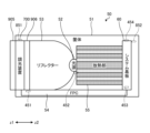
- FIG. 1 is a schematic diagram showing the main configuration of the illumination device 50.
- the lighting device 50 includes a housing 51 , a light source 52 , a reflector 53 , a light control device 700 , an FPC (Flexible Printed Circuits) 54 , a system board 60 and a heat dissipation section 55 .
- the housing 51 is a housing that houses the light source 52 , the reflector 53 , the light control device 700 , the FPC 54 , the system board 60 , and the heat dissipation section 55 .
- the housing 51 is desirably made of a material (for example, aluminum) having excellent heat dissipation properties.
- the light source 52 emits light in response to power supply.
- the light source 52 is, for example, an LED (light emitting diode), but may be another form of electric light.
- light source 52 may be an incandescent bulb.
- the reflector 53 guides the light emitted from the light source 52 to the light control device 700 side.
- the light control device 700 side of the reflector 53 is the z1 direction side
- the light source 52 side of the reflector 53 is the z2 direction side.
- the opposite direction of the z1 direction and the z2 direction is defined as the z direction.
- the reflector 53 is an optical member whose opening width in a plan view orthogonal to the z-direction expands in the direction from the z2-direction side where the light source 52 is located toward the z1-direction side.
- the reflector 53 guides the light emitted from the light source 52 to the light control device 700 side by refraction of a prism or the like or mirror finishing of the inner peripheral surface of the divergent shape.
- the FPC 54 includes wiring connected to the liquid crystal panel 1 of the light control device 700, a ground potential line GND and a signal output line Vout(j), which will be described later with reference to FIG.
- System board 60 is a circuit board on which one or more circuits are provided.
- the heat sink 55 includes a structure that facilitates heat radiation from structures provided on the system board 60 . Examples of the configuration include a heat sink and the like.
- the light control device 700 is provided so as to be able to change the degree of transmission and transmission range of the light emitted from the light source 52 and the light emitted from the light source 52 and guided by the reflector 53 .
- the dimming device 700 is provided with a first configuration 905 and a second configuration 906 .
- the first configuration 905 is provided on the reflector 53 side (z1 direction side) of the light control device 700 .
- the second configuration 906 is provided on the opposite side (z2 direction side) of the first configuration 905 with respect to the light control device 700 .
- a second configuration 906 is, for example, a temperature sensor 400 (see FIG. 10).
- the temperature sensor 400 acquires information regarding the temperature of the liquid crystal panel 1 of the light control device 700 .
- FIG. 2 is a schematic diagram showing a configuration example of the light control device 700.
- the light control device 700 has a plurality of liquid crystal panels 1 arranged in the z direction.
- FIG. 2 shows the light control device 700 having four liquid crystal panels 1, but the number of liquid crystal panels 1 is not limited to four and can be changed as appropriate.
- FIG. 1 the liquid crystal panel 1 included in the light control device 700 will be described with reference to FIGS. 3 to 7.
- FIG. 1 is a diagrammatic representation of the liquid crystal panel 1 included in the light control device 700.
- FIG. 3 is a perspective view of the liquid crystal panel 1 according to the embodiment.
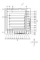
- FIG. 4 is a plan view showing wiring of the array substrate 2 according to the embodiment, and is a view of the array substrate 2 viewed from above.
- FIG. 5 is a plan view showing the wiring of the opposing substrate 3 according to the embodiment, and is a view of the opposing substrate viewed from above.
- FIG. 6 is a plan view showing wiring of the liquid crystal panel 1 according to the embodiment, and is a view of the liquid crystal panel 1 viewed from above.
- 7 is a cross-sectional view taken along line VV of FIG. 6.
- FIG. In addition, in the xyz coordinates shown in FIGS. 3 to 6, the direction along the x1 direction and the x2 direction is referred to as the x direction.
- the x1 direction and the x2 direction are opposite.
- a direction along the y1 direction and the y2 direction is referred to as the y direction.
- the y1 direction and the y2 direction are opposite.
- the x-direction and the y-direction are orthogonal.
- a plane along which the x-direction and the y-direction extend is orthogonal to the z-direction.
- the liquid crystal panel 1 has an array substrate 2 , a counter substrate 3 , a liquid crystal layer 4 and a sealing material 30 .
- the array substrate (first substrate) 2 is larger than the opposing substrate (second substrate) 3. That is, the area of the counter substrate (second substrate) 3 is smaller than the area of the array substrate (first substrate) 2 .
- the array substrate 2 has transparent glass 23 (see FIG. 4).
- the counter substrate 3 has a transparent glass 31 (see FIG. 5).
- the array substrate 2 and the counter substrate 3 are square when viewed from above, but the shape of the substrate according to the present invention is not limited to square.
- a first terminal group area 21 and a second terminal group area 22 are provided on the surface 2 a of the array substrate 2 .
- the first terminal group area 21 is located at the end on the y1 side of the surface 2a of the array substrate 2 .
- the second terminal group area 22 is located at the end of the surface 2a of the array substrate 2 on the x2 side.
- the first terminal group area 21 and the second terminal group area 22 have an L shape when viewed from above.
- the first terminal group 10 is arranged in the first terminal group area 21
- the second terminal group 20 is arranged in the second terminal group area 22 . Since the area of the counter substrate 3 is smaller than that of the array substrate 2, the first terminal group 10 and the second terminal group 20 are exposed. Further, the first terminal group 10 and the second terminal group 20 are also simply referred to as terminal portions.
- the first terminal group 10 includes a first terminal 101, a second terminal 102, a third terminal 103, a fourth terminal 104, a first pad 105, and a second terminal.
- Pad 106 , third pad 107 , fourth pad 108 , fifth pad 109 , sixth pad 110 , seventh pad 111 and eighth pad 112 are included.
- the seventh pad 111 and the eighth pad 112 are arranged side by side in order from the x1 side to the x2 side in the horizontal direction.
- the first pad 105 and the eighth pad 112 are electrically connected via the lead wire 113 .
- the second pad 106 and the seventh pad 111 are electrically connected via the lead wire 113 .
- the third pad 107 and the sixth pad 110 are electrically connected via the lead wire 113 .
- the fourth pad 108 and the fifth pad 109 are electrically connected via the lead wire 113 .
- the second terminal group 20 includes a fifth terminal 201, a sixth terminal 202, a seventh terminal 203, an eighth terminal 204, a ninth pad 205, and a tenth terminal. It includes a pad 206 , an eleventh pad 207 , a twelfth pad 208 , a thirteenth pad 209 , a fourteenth pad 210 , a fifteenth pad 211 and a sixteenth pad 212 .
- the fifteenth pad 211 and the sixteenth pad 212 are arranged side by side in order in the front-rear direction from the y2 side to the y1 side.
- the ninth pad 205 and the sixteenth pad 212 are electrically connected via a lead wire 213 .
- the tenth pad 206 and fifteenth pad 211 are electrically connected via a lead wire 213 .
- the eleventh pad 207 and the fourteenth pad 210 are electrically connected via a lead wire 213 .
- the twelfth pad 208 and the thirteenth pad 209 are electrically connected via a lead wire 213 .
- the counter substrate 3 is arranged above the array substrate 2 (z1 side).
- a sealing material 30 and a liquid crystal layer 4 are provided between the opposing substrate 3 and the array substrate 2 .
- the sealing material 30 is annularly provided along the outer periphery of the opposing substrate 3 , and the inside of the sealing material 30 is filled with the liquid crystal layer 4 .
- the area where the liquid crystal layer 4 is provided is the active area, the outside of the liquid crystal layer 4 is the frame area, and the first terminal group area 21 and the second terminal group area 22 are terminal areas.
- the wiring of the array substrate 2 and the counter substrate 3 will be described.
- the wiring is provided on the front surface of the substrate and the rear surface thereof. That is, the surface on which the wiring is provided is defined as the front surface, and the surface opposite to the front surface is defined as the back surface.
- wiring is provided on the upper surface 2a of the front surface 2a and the rear surface 2b of the array substrate 2, and wiring is provided on the lower surface 3a of the front surface 3a and the rear surface 3b of the counter substrate 3. is provided.
- the surface 2a of the array substrate 2 and the surface 3a of the counter substrate 3 are arranged to face each other with the liquid crystal layer 4 interposed therebetween.
- the wiring 24 and the first electrode 25 are provided on the surface 2a of the transparent glass 23 of the array substrate 2.
- the first terminal 101 and the fifth terminal 201 are electrically connected via the wiring 24 .
- the second terminal 102 and the sixth terminal 202 are electrically connected via the wiring 24 .
- the third terminal 103 and the seventh terminal 203 are electrically connected via the wiring 24 .
- the fourth terminal 104 and the eighth terminal 204 are electrically connected via the wiring 24 .
- a plurality of first electrodes 25 are connected to the wiring 24 that connects the second terminal 102 and the sixth terminal 202 .
- a plurality of first electrodes 25 are connected to the wiring 24 that connects the third terminal 103 and the seventh terminal 203 .
- the wiring 24 is provided with connecting portions C1 and C2.
- the wiring 32 and the second electrode 33 are provided on the surface 3a of the opposing substrate 3. As shown in FIG. Specifically, wirings 32 are provided on the y1 side and the y2 side, respectively. The wiring 32 extends in the x direction. A second electrode 33 is electrically connected to the wiring 32 . The second electrodes 33 extend in the y direction. The wiring 32 is provided with connection portions C3 and C4. In the examples shown in FIGS. 4 to 6, the number of first electrodes 25 and the number of second electrodes 33 are eight. It does not indicate the number of two electrodes 33 . The number of the first electrodes 25 and the number of the second electrodes 33 may be two or more, and naturally may be nine or more.
- the counter substrate 3 is arranged above the array substrate 2 with a space therebetween.
- a liquid crystal layer 4 is filled between the array substrate 2 and the counter substrate 3 .
- the connection portion C1 of the array substrate 2 and the connection portion C3 of the counter substrate 3 are electrically connected via a conductive column (not shown).
- the connection portion C2 of the array substrate 2 and the connection portion C4 of the counter substrate 3 are electrically connected via a conductive column (not shown).
- the first terminal 101, the second terminal 102, the third terminal 103, the fourth terminal 104, the first pad 105, the second pad 106, the third pad 107, and the fourth pad 108 are , can be electrically connected to the FPC 54 indicated by a two-dot chain line.
- the plurality of liquid crystal panels 1 are connected to the D/A converter 64 via, for example, individually provided FPCs 54 .
- the transmittance and transmittance range control of light passing through the liquid crystal panel 1 is realized by controlling the potentials applied to the first electrode 25 and the second electrode 33 .
- the transmittance and transmission range of light passing through the liquid crystal panel 1 are controlled. Note that half of the four liquid crystal panels 1 arranged in the z-direction described with reference to FIG. 2 are p-wave polarized liquid crystal cells, and the other half are s-wave polarized liquid crystal cells.
- Alignment films having different rubbing directions are provided on one surface of the array substrate 2 and one surface of the counter substrate 3 which are opposed to each other with the liquid crystal layer 4 interposed therebetween (not shown).
- the rubbing direction of the alignment film provided on one surface of the array substrate 2 is, for example, the y direction.
- the rubbing direction of the alignment film provided on one surface of the opposing substrate 3 is, for example, the x direction.
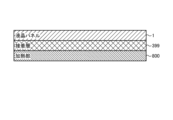
- FIG. 8 is a schematic diagram showing an example of attaching the temperature sensor 400 to the liquid crystal panel 1.
- the adhesive layer 399 is a sheet-like translucent optical member having double-sided adhesiveness such as OCA (Optical Clear Adhesive). Note that the attachment of the temperature sensor 400 to the liquid crystal panel 1 is not limited to the adhesive layer 399, and may be attached using an adhesive, for example.
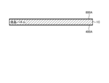
- FIG. 9 is a schematic diagram showing a configuration example of a temperature sensor 400A provided integrally with the liquid crystal panel 1A.
- the liquid crystal panel 1A integrally provided with the function of the liquid crystal panel 1 and the function of the temperature sensor 400 as shown in FIG. may In this case, temperature sensor 400A functions similarly to temperature sensor 400.
- the temperature sensor 400A is laminated on the second electrode 33 on the side of the liquid crystal layer 4 of the opposing substrate 3 via an insulating layer, for example.
- FIG. 10 is a schematic diagram showing an example of an acquisition range of temperature information on the liquid crystal panel 1.
- temperature detection area SA and partial temperature detection area PA refer to areas where temperature information is acquired by temperature sensor 400 or temperature sensor 400A.
- a part of the plate surface of the rectangular liquid crystal panel 1, and an area near one of the four corners may be used as the temperature detection area SA.
- An area covering most of the plate surface of the rectangular liquid crystal panel 1 may be used as the temperature detection area SA.
- a plurality of partial temperature detection areas PA may be arranged within the board surface of the rectangular liquid crystal panel 1 .
- the temperature sensor 400 provided as a configuration corresponding to example P4 in FIG. 10 will be described below with reference to FIG.
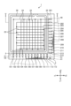
- FIG. 11 is a schematic diagram showing the main configuration and control device of the temperature sensor 400.
- the temperature sensor 400 has a sensor substrate 402 and a sensor section 403 .
- the sensor base 402 has a temperature detection area SA and a peripheral area GA.
- the temperature detection area SA includes a plurality of partial temperature detection areas PA.
- a plurality of partial temperature detection areas PA are areas in which a plurality of temperature detection resistors ER of the sensor section 403 are provided. Note that the z-direction is also the normal direction of the sensor substrate 402 .
- the temperature detection resistor ER is an electric resistance made of an alloy, a compound containing a metal (metallic compound), or a metal.
- the temperature detection resistor ER may be a laminate in which a plurality of types of materials corresponding to at least one of metals, alloys, and metallic compounds are laminated.
- alloy or the like refers to a material that can be employed as the composition of the temperature detection resistor ER and a heating resistor 811, which will be described later.
- the temperature detection resistor ER has a configuration in which a plurality of L-shaped wirings having long sides along the y direction are connected in the x direction. In this aspect, a plurality of L-shaped wirings are connected such that short sides of two L-shaped wirings adjacent in the x-direction are alternated in the y-direction to form the form of the temperature detection resistor ER. It is
- the peripheral area GA is an area between the outer circumference of the temperature detection area SA and the edge of the sensor base 402, and is an area where the temperature detection resistor ER is not provided.
- a plurality of reference resistance elements 401 are provided in the peripheral area GA.
- a temperature sensor is composed of the temperature detection resistor ER provided in the partial temperature detection area PA and the reference resistance element 401 provided in the peripheral area GA.
- the temperature detection resistor ER and the reference resistance element 401 are connected to wiring provided on the FPC 54 .
- Wiring included in the FPC 54 is connected to the system board 60 .
- the wiring provided on the FPC 54 includes a ground potential line GND, a signal input line Vin, and a signal output line Vout.
- a plurality of signal output lines are provided corresponding to the number of temperature detection resistors ER, such as signal output lines Vout(1), Vout(2), . . . , Vout(15). encompasses
- a ground potential line GND shown in FIG. 11 is connected to one end of the temperature detection resistor ER.
- a ground potential line GND applies a ground potential to the temperature detection resistor ER.
- a signal input line Vin is connected to one end of the reference resistance element 401 .
- the signal output line Vout is connected to the other end of the temperature detection resistor ER and the other end of the reference resistance element 401 .
- a drive signal for the temperature sensor 400 is input from the signal input line Vin.
- the drive signal is output to the signal output line Vout via the temperature sensor 400 .
- the strength of the signal output from the signal output line Vout depends on the temperature of the temperature detection resistor ER connected to the signal output line Vout. That is, the temperature of the partial temperature detection area PA provided with the temperature detection resistor ER can be detected based on the signal output from the signal output line Vout.
- the number of electrical resistance elements provided as the reference resistance element 401 and the number of signal output lines Vout correspond to the number of temperature detection resistors ER.
- the plurality of electrical resistance elements are connected in parallel to one signal input line Vin.
- the number of temperature detection resistors ER is not limited to 15, and can be changed as appropriate.
- the specific form of the temperature sensor 400, such as the wiring shape of the temperature detection resistor ER is not limited to this, and can be changed as appropriate.
- the temperature sensor provided in the lighting device 50 is the temperature sensor 400. Further, a sensor for acquiring information indicating the temperature of each part of the lighting device 50 is provided. may be As a specific example, any one of the temperature sensors 451, 452, 453, and 454 shown in FIG. 1 may be provided.
- the temperature sensor 451 is provided in the FPC 54 at a position extremely close to the light control device 700 . Since the temperature sensor 451 can function very similarly to the temperature sensor 400 described with reference to FIG. The temperature may be treated as the temperature of the liquid crystal panel 1 of the light control device 700 .
- the temperature sensor 452 is provided at a position in contact with or close to the light source 52 .
- the temperature sensor 453 is provided at a position in contact with or close to the circuit provided on the system board 60 .
- a temperature sensor 454 is provided in the housing 51 .
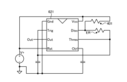
- FIG. 12 is a diagram showing a voltage dividing circuit composed of the temperature detection resistor ER and the reference resistor element 401.
- FIG. The temperature detection resistor ER and the reference resistance element 401 described with reference to FIG. 11 constitute a voltage dividing circuit as shown in FIG.
- the signal output lines Vout(1), Vout(2), . . . , Vout(15) described above can be regarded as output lines of the voltage dividing circuit. Since the electrical resistance value of the reference resistance element 401 is fixed, the output from the signal output line Vout(k) of the voltage dividing circuit depends on the electrical resistance value of the temperature detection resistor ER functioning as a variable resistor.
- the electrical resistance value of the temperature detection resistor ER corresponds to the temperature of the temperature detection resistor ER.
- the magnitude of the output from the signal output line Vout(k) corresponds to the temperature at the location where the temperature detection resistor ER is provided. Accordingly, by providing the temperature sensor 400 including the temperature detection resistor ER in the liquid crystal panel 1, information regarding the temperature at the location where the temperature detection resistor ER is provided can be obtained based on the output from the signal output line Vout(k). can get.
- k is any natural number equal to or less than j.
- the term "voltage dividing circuit described with reference to FIG. 12" includes the reference resistance element 401 and the temperature detecting resistor ER, and the output is a divided voltage corresponding to the temperature of the temperature detecting resistor ER. Point to the circuit.
- FIG. 13 is a graph showing an example of the relationship between the temperature of the temperature detection resistor ER in the voltage dividing circuit described with reference to FIG. 12 and the voltage of the electrical signal obtained as the output of the voltage dividing circuit.
- the electrical resistance value on the ground (GND) side of the voltage dividing circuit described with reference to FIG. 12 increases, and the output voltage of the voltage dividing circuit increases.
- the analog signal output from the signal output line Vout (k) is converted into a digital signal, and the temperature indicated by the digital signal is derived by software processing or circuit logic based on an algorithm similar to the software processing. Processing is performed by circuitry provided on the integrated circuit.
- a configuration for converting an analog signal into a digital signal and the integrated circuit may be the same (for example, an MCU 62 to be described later) or may be separate.
- the configuration of the temperature sensor 400 corresponding to the example P4 of FIG. 10 has been described.
- ER temperature detection resistor
- the partial temperature detection area PA temperature detection resistor ER
- the sensor substrate 402 of the temperature sensor 400 shown in FIG. 11 is replaced with the substrate of the liquid crystal panel 1 (for example, the opposing substrate 3).
- the output from the signal output line Vout(k) is transmitted to the circuit provided on the system board 60 via the FPC 54 .
- a circuit provided on the system board 60 performs temperature rise suppression control. Temperature rise suppression control is operation control of the illumination device 50 that is performed to suppress a further rise in the temperature of the liquid crystal panel 1 .
- a multiplexer may be provided on the signal output path from the signal output line Vout(j).
- the configuration for example, the circuit provided on the system board 60
- the configuration that receives the output from the signal output line Vout(k) can reduce the number of terminals for receiving the output.
- the signal output line Vout(j) and the configuration may be individually connected.
- the temperature of the light control device 700 decreases due to the environment. can be detected more quickly by the temperature sensor 400 .
- the temperature sensor 400 may be provided as the second configuration 906 instead of the first configuration 905 .
- the temperature rise of the light control device 700 which may rise due to the radiation heat from the component provided on the z2 direction side with respect to the light control device 700, is Sensor 400 facilitates faster detection.
- the configuration provided on the z2 direction side with respect to the light control device 700 refers to the light source 52 and the circuits provided on the system board 60, which will be described later.
- the heating unit 800 is provided as the first component 905 .
- the first configuration 905 is the heating unit 800, in an environment where the outside air of the lighting device 50 is low enough to affect the operation of the light control device 700 (for example, less than a predetermined temperature described later), the influence Among the plurality of liquid crystal panels 1 included in the light control device 700, the z1 direction side of the liquid crystal panel 1 positioned closest to the z1 direction side, which receives a relatively large amount of heat, can be heated more quickly.
- the heating unit 800 is provided as the second configuration 906, for example.
- the second structure 906 is the heating unit 800, intensive and rapid heating including the effect of heating the light control device 700 by radiant heat from the structure provided on the z2 direction side with respect to the light control device 700 is performed. can do
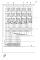
- FIG. 14 is a schematic diagram showing an arrangement example of the heating area HA and the partial heating area HPA with respect to the liquid crystal panel 1.
- the heating range HA and the partial heating range HPA refer to the range in which the heating resistor 811 of the heating unit 800 or the heating resistor 811 of the heating unit 801 is provided.
- a portion of the plate surface of the rectangular liquid crystal panel 1, and an area near one of the four corners may be set as the heating range HA.
- a region covering most of the plate surface of the shaped liquid crystal panel 1 may be set as the heating range HA.
- a plurality of partial heating areas HPA may be arranged within the plate surface of the rectangular liquid crystal panel 1 .
- the partial heating range HPA provided as a configuration corresponding to example P7 in FIG. 14 will be described below with reference to FIG.
- FIG. 15 is a schematic diagram showing a heating resistor 811 provided in the partial heating area HPA and a configuration connected to the heating resistor 811.
- the heating resistor 811 is an electrical resistor made of an alloy or the like.
- the heating resistor 811 has a form in which a plurality of L-shaped wirings with long sides along the y direction are connected in the x direction.
- the heating resistor 811 is formed by connecting a plurality of L-shaped wirings such that the short sides of two L-shaped wirings adjacent in the x direction are alternated in the y direction.
- the wiring 812 is individually provided for each heating resistor 811 and connected to one end of the wiring of each heating resistor 811 .
- the wiring 813 is connected to the other ends of the wirings of the plurality of heating resistors 811 .
- the wiring 812 and the wiring 813 are not directly connected, but connected via the heating resistor 811 .
- the wiring 812 and the wiring 813 are formed in different wiring layers stacked with an insulating layer interposed therebetween.
- the heating resistor 811 may be formed in the same layer as either one of the wiring 812 and the wiring 813, or may be formed in a layer different from the wiring 812 and the wiring 813.
- the heating unit 801 can be employed instead of the heating unit 800.
- the heating unit 801 includes a heating resistor 811, wiring 812, and wiring 814.
- the wiring 814 is individually provided for each heating resistor 811 and connected to the other end of the wiring of each heating resistor 811 .
- the wiring 812 is connected to either the anode or the cathode of the power supply.
- the wiring 813 and the wiring 814 are connected to the other of the anode or cathode of the power supply.
- the configuration corresponding to example P7 in FIG. 14 has been described.
- the heating range HA has the same configuration as one partial heating range HPA.
- FIG. 16 Next, a specific example of providing the heating unit 800 in the liquid crystal panel 1 will be described with reference to FIGS. 16 to 22.
- FIG. 16
- FIG. 16 is a schematic diagram showing an example of attaching the heating unit 800 to the liquid crystal panel 1.
- the liquid crystal panel 1 and the heating section 800 are bonded via an adhesive layer 399, for example.
- the attachment of the heating unit 800 to the liquid crystal panel 1 is not limited to the adhesive layer 399, and may be attached using an adhesive, for example.
- FIG. 17 is a schematic diagram showing a configuration example of a heating section 800A provided integrally with the liquid crystal panel 1B.
- the heating section 800A functions similarly to the heating section 800.
- the heating unit 800A has a heating resistor 811, a wiring 812, and a wiring 813 or 814, which are laminated on the second electrode 33 via an insulating layer, for example, on the liquid crystal layer 4 side of the opposing substrate 3.
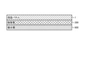
- FIG. 18 is a schematic diagram showing a configuration example when the liquid crystal panel 1 is provided with the temperature sensor 400 and the heating section 800.
- a heating unit 800 may be provided on one side of the plate surface of the liquid crystal panel 1, and a temperature sensor 400 may be provided on the other side.
- An adhesive layer 399 A is interposed between the liquid crystal panel 1 and the heating section 800 .
- An adhesive layer 399 B is interposed between the liquid crystal panel 1 and the temperature sensor 400 .
- the adhesive layers 399A and 399B have the same configuration as the adhesive layer 399 described above.
- FIG. 19 is a schematic diagram showing a liquid crystal panel 1C in which the function of the liquid crystal panel 1, the function of the temperature sensor 400, and the function of the heating section 800 are integrally provided.
- the temperature sensor 400A described with reference to FIGS. 9 to 12 is provided on one side of the liquid crystal panel 1, and the heating unit 800A described with reference to FIGS. It may be provided on the other side of the panel 1 .
- the temperature sensor 400A may be formed on the opposing substrate 3 or may be formed on the array substrate 2 as described with reference to FIG.
- the temperature sensor 400A may be laminated with the first electrode 25 or the second electrode 33 via an insulating layer, for example, on the liquid crystal layer 4 side, or may It may be formed on the plate surface opposite to the plate surface facing the liquid crystal layer 4 .
- the heating portion 800A is formed on the other of the array substrate 2 and the counter substrate 3 on which the temperature sensor 400A is not formed.
- the heating part 800A may be laminated with the first electrode 25 or the second electrode 33 via an insulating layer, for example, or may be stacked on the other plate surface of the array substrate 2 or the counter substrate 3 facing the liquid crystal layer 4. may be formed on the plate surface on the opposite side of the .
- FIG. 20 is a schematic diagram showing a liquid crystal panel 1D in which the function of the liquid crystal panel 1, the function of the temperature sensor 400, and the function of the heating section 800 are integrally provided.
- the partial temperature detection area PA described with reference to FIGS. 10 and 11 and the partial temperature detection area PA described with reference to FIGS. and the partial heating range HPA described above may be alternately arranged.
- the partial temperature detection area PA and the partial heating area HPA can be provided on one surface side of the liquid crystal panel 1D.
- the temperature detection resistor ER (see FIG. 11) may be used as the heating resistor 811 (see FIG. 15).
- the detection period during which the temperature of the liquid crystal panel 1 is detected based on the electrical resistance value of the temperature detection resistor ER and the temperature detection resistor ER are supplied with power when heating is required.
- a so-called time-division control is performed in which a heating period in which the liquid crystal panel 1 is heated by the heat generated by the ER alternately occurs temporally. Note that power is supplied to the temperature detection resistor ER during the heating period when heating is required. That is, when heating is unnecessary, power is not supplied to the temperature detection resistor ER during the heating period.
- the determination as to whether or not heating is necessary is performed, for example, based on a predetermined temperature threshold. Specifically, when the temperature of the liquid crystal panel 1 detected during the detection period is equal to or lower than the temperature threshold, it is determined that heating is necessary, and otherwise, it is determined that heating is unnecessary.
- Various processes related to determination are performed by a circuit provided on the system board 60, for example.
- FIG. 21 is a schematic diagram showing a configuration in which the temperature sensor 400 in FIG. 8 is replaced with a temperature sensor/heating unit 900.
- the temperature sensor/heating unit 900 is configured such that the temperature detection resistor ER (see FIG. 11) of the temperature sensor 400 can be used as the heating resistor 811 (see FIG. 15) of the heating unit 800.
- FIG. Specifically, a closed circuit including the temperature detection resistor ER is provided so as to be switchable between a first path including the reference resistance element 401 and a second path not including the reference resistance element 401 .
- the closed circuit when the first path is established functions as the voltage dividing circuit described with reference to FIG.
- the temperature detection resistor ER In the closed circuit when the second circuit is established, the temperature detection resistor ER is connected to the wiring 812 and the wiring 813 or 814 in the same manner as the heating resistor 811 described with reference to FIG. , and the temperature detection resistor ER generates heat by applying a current to the temperature detection resistor ER and functions in the same manner as the heating resistor 811 .
- FIG. 22 is a schematic diagram showing a configuration in which the temperature sensor 400A in FIG. 9 is replaced with a temperature sensor/heating unit 900A.
- the function of the liquid crystal panel 1 and the function of the temperature sensor/heating unit 900 are integrally provided as shown in FIG.
- the liquid crystal panel 1 ⁇ /b>E may be provided in the light control device 700 .
- the temperature sensor/heating unit 900A functions in the same manner as the temperature sensor/heating unit 900 does.
- the temperature sensor/heating unit 900A is formed on the array substrate 2 or the counter substrate 3 in the same manner as the temperature sensor 400A described above.
- the configuration for heating the lighting device 50 is not limited to these.
- at least one of the heating units 851 and 852 in FIG. 1 may be further provided.
- the heating unit 851 is provided at a position in contact with or close to the light control device 700 on the side of the light control device 700 that does not face the plate surface.
- the heating part 852 is provided at a position that contacts or is close to the system board 60 .
- the temperature of the light control device 700 can easily be adjusted to a temperature more suitable for the operation of the light control device 700. Become.
- the heating unit 852 can heat the circuit. , the temperature is more likely to be suitable for the operation of the circuit.
- the first configuration 905 is provided on the liquid crystal panel 1 closest to the z1 direction among the liquid crystal panels 1 of the light control device 700 .
- the second configuration 906 is provided on the liquid crystal panel 1 closest to the z2 direction among the liquid crystal panels 1 included in the light control device 700 .
- FIG. 23 is a block diagram showing a main configuration example of the system board 60.
- the system board 60 includes, for example, a communication unit 61, an MCU (Micro Controller Unit) 62, an FPGA (Field Programmable Gate Array) 63, a D (Digital)/A (Analog) conversion unit 64, and a light source drive unit 65. and a connecting portion 66 are provided.
- the communication unit 61 communicates with the external information processing device 300 .
- the communication unit 61 has, for example, a circuit that functions as a NIC (Network Interface Controller).
- the communication unit 61 receives a signal including a command regarding the operation of the lighting device 50 transmitted from the information processing device 300 and outputs information indicating the command to the MCU 62 .
- the information processing device 300 is, for example, a mobile terminal such as a smart phone, but is not limited to this.
- the information processing device 300 may be a stationary information processing device such as a server or a PC (Personal Computer) provided for controlling the lighting device 50, or information in another form not illustrated here. It may be a processing device.
- the command related to the operation of the lighting device 50 transmitted from the information processing device 300 is, for example, a command specifying ON/OFF of light irradiation by the lighting device 50, a light irradiation range, a light intensity, and the like. , and any items that can be specified individually within the operation control range of the lighting device 50 can be included in the command.
- the MCU 62 outputs various signals to the FPGA 63 , the light source drive section 65 and the connection section 66 in accordance with the command regarding the operation of the lighting device 50 obtained from the information processing device 300 via the communication section 61 . That is, the MCU 62 controls various components of the lighting device 50 so that the lighting device 50 operates according to the operation from the information processing device 300 .
- the MCU 62 acquires the output from the signal output line Vout(k), and when the output indicates that the temperature of the liquid crystal panel 1 has reached or exceeded a predetermined temperature, the MCU 62 performs temperature rise suppression control. .
- the MCU 62 also controls the operation of the heater HEA.
- the heater HEA is, for example, the heating unit 800, but is not limited to this, and may be any one or more of the heating units 800A, 851, 852, or the partial heating unit described with reference to FIG. It may be the range HPA, or it may be the temperature sensor/heating unit 900 or the temperature sensor/heating unit 900A described with reference to FIGS. Alternatively, a heater may be provided in the heat radiation part 55 to apply heat to the light control device 700 from the heat radiation part 55 .
- the FPGA 63 performs information processing for controlling the operation of the light control device 700 under the control of the MCU 62 and outputs a signal indicating the result of the information processing to the D/A converter 64 . For example, if the instruction regarding the operation of the lighting device 50 transmitted from the information processing device 300 includes a designation regarding the irradiation range of light, the FPGA 63 adjusts the light so that the irradiation range corresponding to the designation is irradiated with light. Information processing for operating the device 700 is performed.
- the D/A conversion unit 64 is configured to output analog signals for operating the plurality of liquid crystal panels 1 included in the light control device 700 based on the digital signals from the FPGA 63 .
- the configuration may consist of one circuit or may include multiple circuits.
- the light source drive unit 65 is a controller that performs ON/OFF control of the light source unit 52 and light emission intensity control when the light source unit 52 is ON under the control of the MCU 62 .
- the controller may be a single circuit or may include multiple circuits.
- connection unit 66 is an interface that connects the MCU 62 and the input/output of the temperature sensor SEN (the ground potential line GND, the signal input line Vin, and the signal output line Vout described above). Also, the connecting portion 66 is connected to the MCU 62 and intervenes in the signal transmission path between the MCU 62 and the temperature sensor SEN.
- the temperature sensor SEN is, for example, the temperature sensor 400, but is not limited to this, and may be any one or more of the temperature sensors 400A, 451, 452, 453, and 454. See FIG. It may be the partial temperature detection area PA described above, or the temperature sensor/heating unit 900 described with reference to FIGS. 19 and 20 .
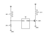
- FIG. 24 is a diagram showing a main circuit configuration example when linking the direct current flowing to the heating resistor and temperature measurement.
- MCU 62 is connected to the voltage dividing circuit and switch SW1 described with reference to FIG.
- the output of the voltage dividing circuit described with reference to FIG. 12 is input to the MCU 62 as an analog signal indicating the temperature of the temperature detection resistor ER.
- the analog signal is converted into a digital signal via an A/D converter (ADC: Analog Digital Converter) that the MCU 62 has.
- ADC Analog Digital Converter
- the MCU 62 outputs a PWM (Pulse Width Modulation) signal corresponding to the temperature of the temperature detection resistor ER indicated by the digital signal to the switch SW1.
- PWM Pulse Width Modulation
- the switch SW1 is a switching element provided on the DC current path in which the heating resistor 811 is provided.
- the switch SW1 opens and closes the DC current path according to the PWM signal. Thereby, the degree of heat generation by the heating resistor 811 is controlled.
- the switch SW1 is, for example, a MOSFET (Metal Oxide Semiconductor Field Effect Transistor), but may be another element that functions similarly.
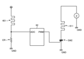
- FIG. 25 is a diagram showing a main circuit configuration example in the case of linking the AC current flowing through the heating resistor and the temperature measurement.
- MCU 62 is connected to the voltage dividing circuit and switch SW2 described with reference to FIG.
- the MCU 62 outputs a PWM signal corresponding to the temperature of the temperature detection resistor ER indicated by the digital signal to the switch SW2.
- the switch SW2 is provided on the alternating current path in which the heating resistor 811 is provided.
- the switch SW2 opens and closes the AC current path according to the PWM signal. Thereby, the degree of heat generation by the heating resistor 811 is controlled.
- the switch SW2 is, for example, a bidirectional thyristor such as a TRIAC (TRIode AC switch), but may be another element that functions similarly.
- TRIAC TRIode AC switch
- the configuration described with reference to FIG. 25 is the same as the configuration described with reference to FIG. 24, except for the items noted above.
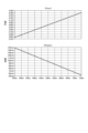
- FIG. 26 is a graph showing an example of the relationship between the pulse width of the PWM signal and the voltage applied to the heating resistor 811.
- FIG. 26 the voltage per unit time applied to the heating resistor 811 rises and falls according to the duty ratio of the PWM signal given from the MCU 62 to the switch SW1 or switch SW2. As the period during which the output of the PWM signal is not 0 increases within the unit time, the voltage applied to the heating resistor 811 increases within the unit time, and the degree of heat generation by the heating resistor 811 increases.
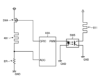
- FIG. 27 is a diagram showing a circuit configuration example that employs a digital potentiometer as a configuration for controlling the amount of heat generated by the heating resistor 811.
- FIG. When the switch SW3, which is a digital potentiometer, is employed in place of the switch SW1 in the configuration described with reference to FIG. A signal (control signal) for controlling the resistance value is output to the switch SW3.
- the switch SW3 causes an electrical resistance value corresponding to the control signal to be generated on the DC current path provided with the heating resistor 811 . Thereby, the degree of heat generation by the heating resistor 811 is controlled.
- the configuration described with reference to FIG. 27 is the same as the configuration described with reference to FIG. 24, except for the items noted above.
- FIG. 28 is a graph showing the relationship in which the current flowing through the heater decreases as the potential of the portion divided by the digital potentiometer and heater increases.
- the degree of heat generation by the heating resistor 811 increases.
- FIG. 29 is a diagram showing a circuit configuration example in which power consumption is reduced by adding ON/OFF circuits for the temperature sensor and the heater individually and turning each ON/OFF.
- the MCU 62A shown in FIG. 29 has a GPIO (General Purpose Input/Output) input/output function in addition to the functions of the configuration of the MCU 62 described with reference to FIG. In the configuration shown in FIG. 29, the GPIO is used as a port for controlling the operation of switch SW4.
- GPIO General Purpose Input/Output
- the switch SW4 is a load switch IC (Integrated Circuit) provided between the reference resistance element 401 in the voltage dividing circuit described with reference to FIG. 12 and the power supply of the voltage dividing circuit.
- the MCU 62A controls ON/OFF of the voltage dividing circuit described with reference to FIG. 12 by controlling ON/OFF of the switch SW4. For example, when the time-division control described above is performed, operation control is adopted in which the voltage dividing circuit is turned on during the detection period and turned off during the heating period.
- a switch SW5 is adopted instead of the switch SW1.
- the switch SW5 is a photocoupler.
- the switch SW5 opens and closes the AC current path provided with the heating resistor 811 according to the duty ratio of the PWM signal given from the MCU 62, like the switch SW1.
- the configuration described with reference to FIG. 29 is the same as the configuration described with reference to FIG. 24, except for the items noted above.
- FIG. 30 is a diagram showing a circuit configuration example for converting the output of the voltage dividing circuit into a pulse wave.
- the timer IC 621 shown in FIG. 30 converts the output of the voltage dividing circuit described with reference to FIG. 12 obtained from the input terminal Disc into a pulse wave and outputs it from the output terminal Out.
- the frequency of the pulse wave corresponds to the magnitude of the output of the voltage dividing circuit described with reference to FIG. Specifically, when the temperature of the temperature detection resistor ER is higher, the electrical resistance value of the temperature detection resistor ER is increased. The higher the electrical resistance value of the temperature detection resistor ER, the lower the frequency of the pulse wave.
- the ADC can be omitted from the MCU 62. That is, by providing a timer IC 621 between the voltage dividing circuit described with reference to FIG.
- the pulse wave output from the timer IC 621 is, for example, a rectangular wave, but may be another pulse wave that can be used as a digital signal.
- FIG. 31 shows a circuit configuration example for controlling the magnitude of the current flowing through the heating resistor 811 according to the output of the voltage dividing circuit described with reference to FIG. 12 without using an MCU such as the MCU 62. It is a diagram.
- a comparator COMP is provided as a configuration for receiving the output of the voltage dividing circuit described with reference to FIG. Comparator COMP provides switch SW6 with an output corresponding to the result of comparison between the output of the voltage dividing circuit described with reference to FIG. 12 and the output of setting circuit SET indicating a predetermined electrical resistance value.
- the switch SW6 opens and closes the alternating current path provided with the heating resistor 811 according to the output of the comparator COMP.
- the configuration described with reference to FIG. 31 is the same as the configuration described with reference to FIG. 24, except for the items noted above.
- Fig. 32 is a graph showing the heater OFF when the temperature sensor reaches 25°C, and is a graph showing a series of operations when SET in Fig. 31 is set to 1V.
- the comparator COMP opens and closes the switch SW6 according to the comparison result between the output voltage and the output voltage of the setting circuit SET. In FIG. 32, when the temperature of the temperature detection resistor ER is 25° C.
- the threshold Thr for switching ON/OFF of the current to the heating resistor 811 is 25° C., but the threshold Thr depends on the output voltage of the setting circuit SET and can be set to any temperature. can.
- FIG. 33 is a diagram showing an example of realizing precise resistance value measurement by detecting the potential difference between both ends of the temperature detection resistor ER in measurement using a differential amplifier circuit.
- a differential amplifier that produces an output corresponding to the difference between the output voltage of the voltage dividing circuit described with reference to FIG. 12 and the voltage on the ground (GND) side of the voltage dividing circuit.
- DifA is provided.
- the heating resistor 811 can generate heat according to the output of the voltage dividing circuit described with reference to FIG.
- FIG. 34 is a graph showing an example of the relationship between the temperature of the temperature detection resistor ER, the output voltage of the voltage dividing circuit described with reference to FIG. 12, the sensor output, and the heater input. It should be noted that the sensor output in FIG. 34 refers to the current generated according to the difference between the voltage on the ground (GND) side of the voltage dividing circuit. A heater input indicates a current flowing through the heating resistor 811 . As shown in FIG. 34, as the temperature rises, the sensor output increases and the heater input decreases.
- the configuration may be the FPGA 63, the MCU 62, or a dedicated configuration (not shown).
- FIG. 35 is a flowchart showing the processing flow of the operation of the lighting device 50.
- step S1 each component provided on the system board 60 performs an initial operation (step S2).
- step S2 the MCU 62 performs processing corresponding to the operation mode so that the illumination device 50 operates in the operation mode (emission intensity, light distribution range, etc.) specified by the signal transmitted from the information processing device 300.
- the FPGA 63 , the light source driving section 65 and the like start operating under the operation control of the MCU 62 .
- step S3 the light control device 700 operates (step S3), and the light transmittance of the light control device 700 is controlled so that the light distribution range specified by the operation mode described above is irradiated with light. .
- step S3 the light source 52 is turned on (step S4).
- step S5 temperature measurement is performed (step S5).
- the MCU 62 operates the temperature sensor 400 and obtains information about the temperature of the liquid crystal panel 1 by obtaining an output from the signal output line Vout(k). Data indicating the correspondence relationship between the magnitude of the output from the signal output line Vout(k) and the temperature of the liquid crystal panel 1 provided with the temperature sensor 400 is obtained in advance by experiment or the like.
- the MCU 62 determines whether a temperature lower than the predetermined temperature is measured in the process of step S5 (step S6). When the temperature below the predetermined temperature is measured (step S6; Yes), the MCU 62 performs heat treatment (step S7).
- FIG. 36 is a flow chart showing the flow of the heat treatment (step S7) in FIG.
- step S7 the temperature of ⁇ 20° C. or less is measured in the process of step S5 described above (step S11; Yes)
- the MCU 62 turns off the operation of the light control device 700 (step S12).
- the heating resistor 811 is driven at a predetermined maximum heat generating capacity (100%) (step S13).
- a state in which the heating resistor 811 is driven with a predetermined maximum heat generation capacity (100%) means a state in which the maximum current within the range of current allowed by the heating resistor 811 is applied to the heating resistor 811 .
- step S5 if the temperature of -20°C or lower is not measured (step S11; No), the MCU 62 turns on the operation of the light control device 700 (step S14). In addition, according to a predetermined heater operation setting (step S15), the heater is driven according to the heater operation setting (step S16).
- FIG. 37 is a diagram showing an example of predetermined heater operation settings described as the operation of step S15.
- ⁇ 20° C. or less is measured as the temperature of the temperature detection resistor ER, it is driven at a predetermined maximum heat generation capacity (100%), and when ⁇ 20° C. or higher and ⁇ 10° C. or less is measured. is driven at 75% of the predetermined maximum heat generation capacity when the 30% of the maximum predetermined heat generation capacity when measured above 0°C and below 0°C, and 10% of the maximum predetermined heat generation capacity when measured above 0°C and below 10°C. % driven settings are shown.
- the heater operation setting described with reference to FIG. 37 is merely an example and is not limited to this, and can be changed as appropriate.
- step S7 After the heating process (step S7) shown in FIG. 35, unless the lighting device 50 is powered off (step S8; No), the process proceeds to step S5 again.
- step S8; Yes When the lighting device 50 is powered off (step S8; Yes), the operation of the lighting device 50 ends. Also, in the process of step S5, when the temperature below the predetermined temperature is not measured (step S6; No), the process of step S7 is not performed and the process proceeds to the branch of step S8.
- the specific form of the lighting device is not limited to that shown in FIG.
- the lighting device 50A shown in FIG. 38 or the lighting device 50B shown in FIG. 39 may be used.
- FIG. 38 is a schematic diagram showing the main configuration of the illumination device 50A.
- the illumination device 50A includes a third configuration 907 and a fourth configuration 908 instead of the first configuration 905 and the second configuration 906 included in the illumination device 50 described with reference to FIG.
- the third configuration 907 is provided on the opposite side (z1 direction side) of the reflector 53 with respect to the light control device 700 .
- the fourth structure 908 is provided on the z1 direction side with respect to the third structure 907 .
- One of the third configuration 907 and the fourth configuration 908 may be the temperature sensor 400 and the other may be the heating unit 800, but at least one of the third configuration 907 and the fourth configuration 908 may be the other. may be configured.
- Other configurations include, for example, a polarizing plate or a light control mirror.
- a polarizing plate transmits light polarized in a specific direction and blocks light polarized in other directions.
- the polarization direction of light that can pass through the polarizing plate can be arbitrarily determined at the time of design. By shielding part of the light with the polarizing plate, heating by the infrared rays contained in the light can be expected.
- the light control mirror has a structure in which a structure in which the liquid crystal layer in the liquid crystal display panel is an electrochromic layer and a half mirror are laminated.
- the electrochromic layer includes a thin film of electrochromic material such as WO3, NbO5, TiO2, and an electrolyte solution.
- the dimmer mirror has the effect of suppressing yellowing of light and obtaining visibility toward blue.
- the half mirror of the light control mirror is provided so as to reflect part of the light traveling from the z2 direction side to the z1 direction side to the z2 direction side. Heating of the liquid crystal panel 1 by the infrared rays contained in the reflected light can be expected by the light control mirror.
- One of the third structure 907 and the fourth structure 908 is one of the polarizing plate and the light control mirror, and the other of the third structure 907 and the fourth structure 908 is the other of the polarizing plate and the light control mirror.
- a configuration having a heater function may be the third configuration 907, and the polarizing plate or the light control mirror may be the fourth configuration 908. good too.
- the second configuration 906 shown in FIG. may be used as the temperature sensor 400 .
- FIG. 39 is a schematic diagram showing the main configuration of the illumination device 50B.
- the lighting device 50B includes a plurality of light sources.
- FIG. 39 illustrates an illumination device 50B including two light sources 52A and 52B, the illumination device may be provided with three or more light sources.
- the lighting device provided with a plurality of light sources also has a temperature sensor (for example, the temperature sensor 400, etc.) in the same manner as the lighting device 50 described with reference to FIG.
- a temperature sensor for example, the temperature sensor 400, etc.
- the temperature sensor detects a temperature below a predetermined temperature (for example, below 10° C.)
- the plurality of light sources are turned on.
- a predetermined temperature for example, below 10° C.
- a predetermined temperature for example, below 10° C.
- the temperature sensor detects a temperature equal to or higher than a predetermined temperature for example, 10° C. or higher
- a predetermined temperature for example, 10° C. or higher
- the illumination device for example, the illumination devices 50, 50A, and 50B
- the illumination device includes a light source (light source 52) that emits light and at least one liquid crystal panel (liquid crystal panel) on the light emitting side of the light source. It has a panel 1), and adjusts the light distribution range of the light emitted from the liquid crystal panel to the outside by controlling the transmittance of light passing through the liquid crystal panel and the transmission range of light passing through the liquid crystal panel.
- a light control device (light control device 700), a temperature sensor (temperature sensor 400, partial temperature detection area PA or temperature sensor/heating unit 900, 900A) for acquiring information indicating the temperature of the liquid crystal panel, and the liquid crystal panel
- the heating unit (heating unit 800, 801, 800A, temperature sensor/heating unit 900, 900A, partial heating range HPA or multiple light sources) and the temperature sensor obtained information indicating a temperature below a predetermined temperature and a control unit (MCUs 62 and 62A, timer IC 621, comparator COMP or differential amplifier DifA) that operates the heating unit in the case. Therefore, the heating unit can suppress the temperature drop of the liquid crystal panel provided on the emission path of the light from the light source, which is included in the light control device.
- the heating unit since the heating unit is operated when the temperature sensor acquires information indicating a temperature equal to or lower than the predetermined temperature, the heating unit can be appropriately operated when the liquid crystal panel needs to be heated.
- the heating unit (temperature sensor/heating unit 900, 900A or partial heating area HPA) is a heater having a first lead wire unit (heating resistor 811) that generates heat in response to power supply, the liquid crystal panel (liquid crystal panel 1 ) is extremely easy, and the liquid crystal panel can be preferably heated.
- the temperature sensor (temperature sensor 400) has a second conducting wire portion (temperature detecting resistor ER) whose electric resistance value changes with temperature, and the first conducting wire portion (heating resistor 811) and the second conducting wire portion are provided on the same surface of the liquid crystal panel (liquid crystal panel 1) (see, for example, FIGS. 20 to 22).
- a second conducting wire portion temperature detecting resistor ER
- the first conducting wire portion heating resistor 811
- the second conducting wire portion are provided on the same surface of the liquid crystal panel (liquid crystal panel 1) (see, for example, FIGS. 20 to 22).
- the heating unit also supplies power to the second conductor (temperature detection resistor ER) to cause the second conductor to generate heat. As a result, attenuation of light from the light source (light source 52) due to the conducting wire can be further reduced.
- the lighting device (for example, the lighting device 50B) reflects part of the light that has passed through the light control device (light control device 700) from the light source (light source 52 or one of the light sources 52A and 52B) toward the light source side. Equipped with a part (light control mirror). This makes it possible to increase the number of heat sources for heating the light control device.
- the illumination device for example, illumination device 50B
- the light control device includes a polarizing plate that transmits light in a specific polarization direction and blocks light in other polarization directions. This makes it possible to increase the number of heat sources for heating the light control device.
- a plurality of light sources (for example, the light sources 52A and 52B) are provided, and one or more of the plurality of light sources is operated as a heating unit. and the operation for heating the lighting device.
- the specific structure of the light control device 700 is not limited to the example described with reference to FIG.
- the light control device 700 may have a liquid crystal panel functioning as a so-called liquid crystal lens, which is provided so as to be able to change the degree of refraction of light directed from one side to the other side by controlling the light distribution of the liquid crystal. good.
Landscapes
- Physics & Mathematics (AREA)
- Nonlinear Science (AREA)
- Chemical & Material Sciences (AREA)
- Crystallography & Structural Chemistry (AREA)
- General Physics & Mathematics (AREA)
- Optics & Photonics (AREA)
- Mathematical Physics (AREA)
- Engineering & Computer Science (AREA)
- General Engineering & Computer Science (AREA)
- Devices For Indicating Variable Information By Combining Individual Elements (AREA)
- Liquid Crystal (AREA)
Priority Applications (2)
| Application Number | Priority Date | Filing Date | Title |
|---|---|---|---|
| JP2024501058A JPWO2023157602A1 (https=) | 2022-02-18 | 2023-01-26 | |
| US18/793,159 US20240393643A1 (en) | 2022-02-18 | 2024-08-02 | Illumination device |
Applications Claiming Priority (2)
| Application Number | Priority Date | Filing Date | Title |
|---|---|---|---|
| JP2022-024265 | 2022-02-18 | ||
| JP2022024265 | 2022-02-18 |
Related Child Applications (1)
| Application Number | Title | Priority Date | Filing Date |
|---|---|---|---|
| US18/793,159 Continuation US20240393643A1 (en) | 2022-02-18 | 2024-08-02 | Illumination device |
Publications (1)
| Publication Number | Publication Date |
|---|---|
| WO2023157602A1 true WO2023157602A1 (ja) | 2023-08-24 |
Family
ID=87578352
Family Applications (1)
| Application Number | Title | Priority Date | Filing Date |
|---|---|---|---|
| PCT/JP2023/002518 Ceased WO2023157602A1 (ja) | 2022-02-18 | 2023-01-26 | 照明装置 |
Country Status (3)
| Country | Link |
|---|---|
| US (1) | US20240393643A1 (https=) |
| JP (1) | JPWO2023157602A1 (https=) |
| WO (1) | WO2023157602A1 (https=) |
Cited By (1)
| Publication number | Priority date | Publication date | Assignee | Title |
|---|---|---|---|---|
| JP7599057B2 (ja) | 2022-02-21 | 2024-12-12 | 株式会社ジャパンディスプレイ | 照明装置 |
Citations (5)
| Publication number | Priority date | Publication date | Assignee | Title |
|---|---|---|---|---|
| JP2007286611A (ja) * | 2006-03-21 | 2007-11-01 | Semiconductor Energy Lab Co Ltd | バックライト装置及び表示装置 |
| JP2009008941A (ja) * | 2007-06-28 | 2009-01-15 | Lg Display Co Ltd | 液晶表示装置 |
| JP2010039247A (ja) * | 2008-08-06 | 2010-02-18 | Seiko Epson Corp | 電気光学装置及び電子機器 |
| JP2010122435A (ja) * | 2008-11-19 | 2010-06-03 | Sony Corp | 液晶表示装置、バックライトユニットおよび光学フィルタ |
| JP2011508909A (ja) * | 2007-12-28 | 2011-03-17 | スリーエム イノベイティブ プロパティズ カンパニー | 鏡面部分反射体及び円形モード反射偏光子を含むバックライティングシステム |
Family Cites Families (3)
| Publication number | Priority date | Publication date | Assignee | Title |
|---|---|---|---|---|
| JP2021144190A (ja) * | 2020-03-13 | 2021-09-24 | シャープ株式会社 | 表示装置 |
| JPWO2023153165A1 (https=) * | 2022-02-08 | 2023-08-17 | ||
| JP2024078700A (ja) * | 2022-11-30 | 2024-06-11 | セイコーエプソン株式会社 | 液晶装置および電子機器 |
-
2023
- 2023-01-26 JP JP2024501058A patent/JPWO2023157602A1/ja active Pending
- 2023-01-26 WO PCT/JP2023/002518 patent/WO2023157602A1/ja not_active Ceased
-
2024
- 2024-08-02 US US18/793,159 patent/US20240393643A1/en not_active Abandoned
Patent Citations (5)
| Publication number | Priority date | Publication date | Assignee | Title |
|---|---|---|---|---|
| JP2007286611A (ja) * | 2006-03-21 | 2007-11-01 | Semiconductor Energy Lab Co Ltd | バックライト装置及び表示装置 |
| JP2009008941A (ja) * | 2007-06-28 | 2009-01-15 | Lg Display Co Ltd | 液晶表示装置 |
| JP2011508909A (ja) * | 2007-12-28 | 2011-03-17 | スリーエム イノベイティブ プロパティズ カンパニー | 鏡面部分反射体及び円形モード反射偏光子を含むバックライティングシステム |
| JP2010039247A (ja) * | 2008-08-06 | 2010-02-18 | Seiko Epson Corp | 電気光学装置及び電子機器 |
| JP2010122435A (ja) * | 2008-11-19 | 2010-06-03 | Sony Corp | 液晶表示装置、バックライトユニットおよび光学フィルタ |
Cited By (1)
| Publication number | Priority date | Publication date | Assignee | Title |
|---|---|---|---|---|
| JP7599057B2 (ja) | 2022-02-21 | 2024-12-12 | 株式会社ジャパンディスプレイ | 照明装置 |
Also Published As
| Publication number | Publication date |
|---|---|
| US20240393643A1 (en) | 2024-11-28 |
| JPWO2023157602A1 (https=) | 2023-08-24 |
Similar Documents
| Publication | Publication Date | Title |
|---|---|---|
| US9715299B2 (en) | Liquid crystal display device | |
| JPWO2017175796A1 (ja) | 調光モジュール | |
| US10636381B2 (en) | Display device | |
| CN104570472B (zh) | 液晶显示装置 | |
| JP5581029B2 (ja) | 照明モジュール | |
| KR20170015808A (ko) | 터치 패널의 구동 장치 및 이를 포함하는 전자 기기 | |
| WO2023157602A1 (ja) | 照明装置 | |
| US7312583B2 (en) | Apparatus and method for driving a lamp unit, and liquid crystal display device using the same | |
| JP5108418B2 (ja) | 照明システム | |
| JP2011243894A (ja) | 有機el照明装置 | |
| US7151345B2 (en) | Method and apparatus for controlling visual enhancement of luminent devices | |
| US20210096404A1 (en) | Backlight Module, Display Device and Control Method Thereof | |
| US7432659B2 (en) | Back light unit and liquid crystal display device using the same | |
| US20240288155A1 (en) | Illumination device | |
| US20240392951A1 (en) | Illumination device | |
| CN210323664U (zh) | 背光模组和显示装置 | |
| CN113075820A (zh) | 显示设备、控制方法以及光学模组 | |
| WO2006098114A1 (ja) | 表示装置およびこの表示装置を備えるテレビ受信機 | |
| CN110286518B (zh) | 显示模组及其控制方法和显示装置 | |
| CN117218968B (zh) | 一种显示面板、温度控制方法及相关设备 | |
| KR20030060909A (ko) | 가열기 전극을 가지고 있는 el 램프 | |
| US20070222400A1 (en) | Method and apparatus for equalizing current in a fluorescent lamp array | |
| CN117995822A (zh) | 一种芯片失效分析散热测试结构和方法 | |
| TWI341949B (en) | Illuminating device and liquid crystal display | |
| KR20050051913A (ko) | 액정표시장치 |
Legal Events
| Date | Code | Title | Description |
|---|---|---|---|
| 121 | Ep: the epo has been informed by wipo that ep was designated in this application |
Ref document number: 23756130 Country of ref document: EP Kind code of ref document: A1 |
|
| ENP | Entry into the national phase |
Ref document number: 2024501058 Country of ref document: JP Kind code of ref document: A |
|
| NENP | Non-entry into the national phase |
Ref country code: DE |
|
| 122 | Ep: pct application non-entry in european phase |
Ref document number: 23756130 Country of ref document: EP Kind code of ref document: A1 |