WO2023157602A1 - Lighting device - Google Patents
Lighting device Download PDFInfo
- Publication number
- WO2023157602A1 WO2023157602A1 PCT/JP2023/002518 JP2023002518W WO2023157602A1 WO 2023157602 A1 WO2023157602 A1 WO 2023157602A1 JP 2023002518 W JP2023002518 W JP 2023002518W WO 2023157602 A1 WO2023157602 A1 WO 2023157602A1
- Authority
- WO
- WIPO (PCT)
- Prior art keywords
- liquid crystal
- light
- crystal panel
- temperature
- heating
- Prior art date
Links
Images


Classifications
-
- F—MECHANICAL ENGINEERING; LIGHTING; HEATING; WEAPONS; BLASTING
- F21—LIGHTING
- F21S—NON-PORTABLE LIGHTING DEVICES; SYSTEMS THEREOF; VEHICLE LIGHTING DEVICES SPECIALLY ADAPTED FOR VEHICLE EXTERIORS
- F21S2/00—Systems of lighting devices, not provided for in main groups F21S4/00 - F21S10/00 or F21S19/00, e.g. of modular construction
-
- F—MECHANICAL ENGINEERING; LIGHTING; HEATING; WEAPONS; BLASTING
- F21—LIGHTING
- F21V—FUNCTIONAL FEATURES OR DETAILS OF LIGHTING DEVICES OR SYSTEMS THEREOF; STRUCTURAL COMBINATIONS OF LIGHTING DEVICES WITH OTHER ARTICLES, NOT OTHERWISE PROVIDED FOR
- F21V23/00—Arrangement of electric circuit elements in or on lighting devices
-
- F—MECHANICAL ENGINEERING; LIGHTING; HEATING; WEAPONS; BLASTING
- F21—LIGHTING
- F21V—FUNCTIONAL FEATURES OR DETAILS OF LIGHTING DEVICES OR SYSTEMS THEREOF; STRUCTURAL COMBINATIONS OF LIGHTING DEVICES WITH OTHER ARTICLES, NOT OTHERWISE PROVIDED FOR
- F21V29/00—Protecting lighting devices from thermal damage; Cooling or heating arrangements specially adapted for lighting devices or systems
- F21V29/90—Heating arrangements
-
- G—PHYSICS
- G02—OPTICS
- G02F—OPTICAL DEVICES OR ARRANGEMENTS FOR THE CONTROL OF LIGHT BY MODIFICATION OF THE OPTICAL PROPERTIES OF THE MEDIA OF THE ELEMENTS INVOLVED THEREIN; NON-LINEAR OPTICS; FREQUENCY-CHANGING OF LIGHT; OPTICAL LOGIC ELEMENTS; OPTICAL ANALOGUE/DIGITAL CONVERTERS
- G02F1/00—Devices or arrangements for the control of the intensity, colour, phase, polarisation or direction of light arriving from an independent light source, e.g. switching, gating or modulating; Non-linear optics
- G02F1/01—Devices or arrangements for the control of the intensity, colour, phase, polarisation or direction of light arriving from an independent light source, e.g. switching, gating or modulating; Non-linear optics for the control of the intensity, phase, polarisation or colour
- G02F1/13—Devices or arrangements for the control of the intensity, colour, phase, polarisation or direction of light arriving from an independent light source, e.g. switching, gating or modulating; Non-linear optics for the control of the intensity, phase, polarisation or colour based on liquid crystals, e.g. single liquid crystal display cells
-
- H—ELECTRICITY
- H05—ELECTRIC TECHNIQUES NOT OTHERWISE PROVIDED FOR
- H05B—ELECTRIC HEATING; ELECTRIC LIGHT SOURCES NOT OTHERWISE PROVIDED FOR; CIRCUIT ARRANGEMENTS FOR ELECTRIC LIGHT SOURCES, IN GENERAL
- H05B45/00—Circuit arrangements for operating light-emitting diodes [LED]
- H05B45/10—Controlling the intensity of the light
-
- H—ELECTRICITY
- H05—ELECTRIC TECHNIQUES NOT OTHERWISE PROVIDED FOR
- H05B—ELECTRIC HEATING; ELECTRIC LIGHT SOURCES NOT OTHERWISE PROVIDED FOR; CIRCUIT ARRANGEMENTS FOR ELECTRIC LIGHT SOURCES, IN GENERAL
- H05B45/00—Circuit arrangements for operating light-emitting diodes [LED]
- H05B45/30—Driver circuits
- H05B45/32—Pulse-control circuits
- H05B45/325—Pulse-width modulation [PWM]
-
- F—MECHANICAL ENGINEERING; LIGHTING; HEATING; WEAPONS; BLASTING
- F21—LIGHTING
- F21Y—INDEXING SCHEME ASSOCIATED WITH SUBCLASSES F21K, F21L, F21S and F21V, RELATING TO THE FORM OR THE KIND OF THE LIGHT SOURCES OR OF THE COLOUR OF THE LIGHT EMITTED
- F21Y2115/00—Light-generating elements of semiconductor light sources
- F21Y2115/10—Light-emitting diodes [LED]
Definitions
- the present disclosure relates to lighting devices.
- a lighting device that can change the irradiation range of light by providing the direction of the device to be changeable (for example, Patent Document 1).
- the lighting device can be made compact and the light distribution can be controlled. be more flexible.
- the liquid crystal panel has a limited temperature range in which it can operate normally, it is necessary to take countermeasures assuming that the temperature of the liquid crystal panel falls outside that temperature range.
- the present disclosure has been made in view of the above problems, and an object thereof is to provide a lighting device capable of suppressing a temperature drop of a liquid crystal panel provided on an emission path of light from a light source.
- a lighting device includes a light source that emits light and at least one liquid crystal panel on a light output side of the light source, and the transmittance of light passing through the liquid crystal panel and the rate of light passing through the liquid crystal panel are A light control device that adjusts the light distribution range of light emitted from the liquid crystal panel to the outside by controlling the transmission range, a temperature sensor that acquires information indicating the temperature of the liquid crystal panel, and a heater for the liquid crystal panel. and a control unit that operates the heating unit when information indicating a temperature equal to or lower than a predetermined temperature is obtained from the temperature sensor.
- FIG. 1 is a schematic diagram showing the main configuration of an illumination device.
- FIG. 2 is a schematic diagram showing a configuration example of a light control device.
- FIG. 3 is a perspective view of the liquid crystal panel according to the embodiment.
- FIG. 4 is a plan view showing wiring of the array substrate according to the embodiment, and is a view of the array substrate viewed from above.
- FIG. 5 is a plan view showing the wiring of the opposing substrate according to the embodiment, and is a view of the opposing substrate viewed from above.
- FIG. 8 is a schematic diagram showing an example of attaching a temperature sensor to a liquid crystal panel.
- FIG. 9 is a schematic diagram showing a configuration example of a temperature sensor provided integrally with the liquid crystal panel.
- FIG. 10 is a schematic diagram showing an example of an acquisition range of temperature information on a liquid crystal panel.
- FIG. 11 is a schematic diagram showing the main configuration and control device of the temperature sensor.
- FIG. 12 is a diagram showing a voltage dividing circuit composed of a temperature detection resistor and a reference resistor element.
- FIG. 13 is a graph showing an example of the relationship between the temperature of the temperature detection resistor in the voltage dividing circuit described with reference to FIG. 12 and the voltage of the electrical signal obtained as the output of the voltage dividing circuit.
- FIG. 14 is a schematic diagram showing an arrangement example of the heating range and the partial heating range with respect to the liquid crystal panel.
- FIG. 15 is a schematic diagram showing a heating resistor provided in the partial heating range and a configuration connected to the heating resistor.
- FIG. 16 is a schematic diagram showing an example of attachment of the heating unit to the liquid crystal panel.
- FIG. 17 is a schematic diagram showing a configuration example of a heating unit provided integrally with the liquid crystal panel.
- FIG. 18 is a schematic diagram showing a configuration example in which a temperature sensor and a heating section are provided on the liquid crystal panel.
- FIG. 19 is a schematic diagram showing a liquid crystal panel in which the function of the liquid crystal panel, the function of the temperature sensor, and the function of the heating section are integrally provided.
- FIG. 20 is a schematic diagram showing a liquid crystal panel in which the function of a liquid crystal panel, the function of a temperature sensor, and the function of a heating section are integrally provided.
- FIG. 21 is a schematic diagram showing a configuration in which the temperature sensor in FIG. 8 is replaced with a temperature sensor/heating unit.
- FIG. 22 is a schematic diagram showing a configuration in which the temperature sensor in FIG. 9 is replaced with a temperature sensor/heating unit.
- FIG. 23 is a block diagram showing a main configuration example of the system board.
- FIG. 24 is a diagram showing a main circuit configuration example in the case of linking the DC current flowing through the heating resistor and the temperature measurement.
- FIG. 25 is a diagram showing a main circuit configuration example in the case of linking alternating current flowing through the heating resistor and temperature measurement.
- FIG. 26 is a graph showing an example of the relationship between the pulse width of the PWM signal and the voltage applied to the heating resistor.
- FIG. 27 is a diagram showing a circuit configuration example employing a digital potentiometer as a configuration related to heat generation control of a heating resistor.
- FIG. 28 is a graph showing the relationship in which the current flowing through the heater decreases as the potential of the portion divided by the digital potentiometer and heater increases.
- FIG. 29 is a diagram showing a circuit configuration example in which power consumption is reduced by adding an ON/OFF circuit for each of the temperature sensor and the heater and turning each ON/OFF.
- FIG. 29 is a diagram showing a circuit configuration example in which power consumption is reduced by adding an ON/OFF circuit for each of the temperature sensor and the heater and turning each ON/OFF.
- FIG. 30 is a diagram showing a circuit configuration example for converting the output of the voltage dividing circuit into a pulse wave.
- FIG. 31 is a diagram showing a circuit configuration example for controlling the magnitude of the current flowing through the heating resistor according to the output of the voltage dividing circuit described with reference to FIG. 12 without using the MCU.
- FIG. 32 is a graph showing the heater OFF when the temperature sensor reaches 25° C., and is a graph showing a series of operations when SET in FIG. 31 is set to 1V.
- FIG. 33 is a diagram showing an example of realizing precise resistance value measurement by detecting a potential difference between both ends of a temperature detection resistor ER in measurement using a differential amplifier circuit.
- FIG. 31 is a diagram showing a circuit configuration example for controlling the magnitude of the current flowing through the heating resistor according to the output of the voltage dividing circuit described with reference to FIG. 12 without using the MCU.
- FIG. 32 is a graph showing the heater OFF when the temperature sensor reaches 25° C., and
- FIG. 34 is a graph showing an example of the relationship between the temperature of the temperature detection resistor, the output voltage of the voltage dividing circuit described with reference to FIG. 12, the sensor output, and the heater input.
- FIG. 35 is a flow chart showing the processing flow of the operation of lighting device 50 .
- FIG. 36 is a flow chart showing the flow of the heating process (step S7) in FIG.
- FIG. 37 is a diagram showing an example of predetermined heater operation settings described as the operation of step S15.
- FIG. 38 is a schematic diagram showing the main configuration of the lighting device.
- FIG. 39 is a schematic diagram showing the main configuration of the lighting device.
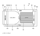
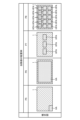
- FIG. 1 is a schematic diagram showing the main configuration of the illumination device 50.
- the lighting device 50 includes a housing 51 , a light source 52 , a reflector 53 , a light control device 700 , an FPC (Flexible Printed Circuits) 54 , a system board 60 and a heat dissipation section 55 .
- the housing 51 is a housing that houses the light source 52 , the reflector 53 , the light control device 700 , the FPC 54 , the system board 60 , and the heat dissipation section 55 .
- the housing 51 is desirably made of a material (for example, aluminum) having excellent heat dissipation properties.
- the light source 52 emits light in response to power supply.
- the light source 52 is, for example, an LED (light emitting diode), but may be another form of electric light.
- light source 52 may be an incandescent bulb.
- the reflector 53 guides the light emitted from the light source 52 to the light control device 700 side.
- the light control device 700 side of the reflector 53 is the z1 direction side
- the light source 52 side of the reflector 53 is the z2 direction side.
- the opposite direction of the z1 direction and the z2 direction is defined as the z direction.
- the reflector 53 is an optical member whose opening width in a plan view orthogonal to the z-direction expands in the direction from the z2-direction side where the light source 52 is located toward the z1-direction side.
- the reflector 53 guides the light emitted from the light source 52 to the light control device 700 side by refraction of a prism or the like or mirror finishing of the inner peripheral surface of the divergent shape.
- the FPC 54 includes wiring connected to the liquid crystal panel 1 of the light control device 700, a ground potential line GND and a signal output line Vout(j), which will be described later with reference to FIG.
- System board 60 is a circuit board on which one or more circuits are provided.
- the heat sink 55 includes a structure that facilitates heat radiation from structures provided on the system board 60 . Examples of the configuration include a heat sink and the like.
- the light control device 700 is provided so as to be able to change the degree of transmission and transmission range of the light emitted from the light source 52 and the light emitted from the light source 52 and guided by the reflector 53 .
- the dimming device 700 is provided with a first configuration 905 and a second configuration 906 .
- the first configuration 905 is provided on the reflector 53 side (z1 direction side) of the light control device 700 .
- the second configuration 906 is provided on the opposite side (z2 direction side) of the first configuration 905 with respect to the light control device 700 .
- a second configuration 906 is, for example, a temperature sensor 400 (see FIG. 10).
- the temperature sensor 400 acquires information regarding the temperature of the liquid crystal panel 1 of the light control device 700 .
- FIG. 2 is a schematic diagram showing a configuration example of the light control device 700.
- the light control device 700 has a plurality of liquid crystal panels 1 arranged in the z direction.
- FIG. 2 shows the light control device 700 having four liquid crystal panels 1, but the number of liquid crystal panels 1 is not limited to four and can be changed as appropriate.
- FIG. 1 the liquid crystal panel 1 included in the light control device 700 will be described with reference to FIGS. 3 to 7.
- FIG. 1 is a diagrammatic representation of the liquid crystal panel 1 included in the light control device 700.
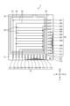
- FIG. 3 is a perspective view of the liquid crystal panel 1 according to the embodiment.
- FIG. 4 is a plan view showing wiring of the array substrate 2 according to the embodiment, and is a view of the array substrate 2 viewed from above.
- FIG. 5 is a plan view showing the wiring of the opposing substrate 3 according to the embodiment, and is a view of the opposing substrate viewed from above.
- FIG. 6 is a plan view showing wiring of the liquid crystal panel 1 according to the embodiment, and is a view of the liquid crystal panel 1 viewed from above.
- 7 is a cross-sectional view taken along line VV of FIG. 6.
- FIG. In addition, in the xyz coordinates shown in FIGS. 3 to 6, the direction along the x1 direction and the x2 direction is referred to as the x direction.
- the x1 direction and the x2 direction are opposite.
- a direction along the y1 direction and the y2 direction is referred to as the y direction.
- the y1 direction and the y2 direction are opposite.
- the x-direction and the y-direction are orthogonal.
- a plane along which the x-direction and the y-direction extend is orthogonal to the z-direction.
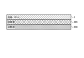
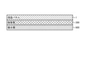
- the liquid crystal panel 1 has an array substrate 2 , a counter substrate 3 , a liquid crystal layer 4 and a sealing material 30 .
- the array substrate (first substrate) 2 is larger than the opposing substrate (second substrate) 3. That is, the area of the counter substrate (second substrate) 3 is smaller than the area of the array substrate (first substrate) 2 .
- the array substrate 2 has transparent glass 23 (see FIG. 4).
- the counter substrate 3 has a transparent glass 31 (see FIG. 5).
- the array substrate 2 and the counter substrate 3 are square when viewed from above, but the shape of the substrate according to the present invention is not limited to square.
- a first terminal group area 21 and a second terminal group area 22 are provided on the surface 2 a of the array substrate 2 .
- the first terminal group area 21 is located at the end on the y1 side of the surface 2a of the array substrate 2 .
- the second terminal group area 22 is located at the end of the surface 2a of the array substrate 2 on the x2 side.
- the first terminal group area 21 and the second terminal group area 22 have an L shape when viewed from above.
- the first terminal group 10 is arranged in the first terminal group area 21
- the second terminal group 20 is arranged in the second terminal group area 22 . Since the area of the counter substrate 3 is smaller than that of the array substrate 2, the first terminal group 10 and the second terminal group 20 are exposed. Further, the first terminal group 10 and the second terminal group 20 are also simply referred to as terminal portions.
- the first terminal group 10 includes a first terminal 101, a second terminal 102, a third terminal 103, a fourth terminal 104, a first pad 105, and a second terminal.
- Pad 106 , third pad 107 , fourth pad 108 , fifth pad 109 , sixth pad 110 , seventh pad 111 and eighth pad 112 are included.
- the seventh pad 111 and the eighth pad 112 are arranged side by side in order from the x1 side to the x2 side in the horizontal direction.
- the first pad 105 and the eighth pad 112 are electrically connected via the lead wire 113 .
- the second pad 106 and the seventh pad 111 are electrically connected via the lead wire 113 .
- the third pad 107 and the sixth pad 110 are electrically connected via the lead wire 113 .
- the fourth pad 108 and the fifth pad 109 are electrically connected via the lead wire 113 .
- the second terminal group 20 includes a fifth terminal 201, a sixth terminal 202, a seventh terminal 203, an eighth terminal 204, a ninth pad 205, and a tenth terminal. It includes a pad 206 , an eleventh pad 207 , a twelfth pad 208 , a thirteenth pad 209 , a fourteenth pad 210 , a fifteenth pad 211 and a sixteenth pad 212 .
- the fifteenth pad 211 and the sixteenth pad 212 are arranged side by side in order in the front-rear direction from the y2 side to the y1 side.
- the ninth pad 205 and the sixteenth pad 212 are electrically connected via a lead wire 213 .
- the tenth pad 206 and fifteenth pad 211 are electrically connected via a lead wire 213 .
- the eleventh pad 207 and the fourteenth pad 210 are electrically connected via a lead wire 213 .
- the twelfth pad 208 and the thirteenth pad 209 are electrically connected via a lead wire 213 .
- the counter substrate 3 is arranged above the array substrate 2 (z1 side).
- a sealing material 30 and a liquid crystal layer 4 are provided between the opposing substrate 3 and the array substrate 2 .
- the sealing material 30 is annularly provided along the outer periphery of the opposing substrate 3 , and the inside of the sealing material 30 is filled with the liquid crystal layer 4 .
- the area where the liquid crystal layer 4 is provided is the active area, the outside of the liquid crystal layer 4 is the frame area, and the first terminal group area 21 and the second terminal group area 22 are terminal areas.
- the wiring of the array substrate 2 and the counter substrate 3 will be described.
- the wiring is provided on the front surface of the substrate and the rear surface thereof. That is, the surface on which the wiring is provided is defined as the front surface, and the surface opposite to the front surface is defined as the back surface.
- wiring is provided on the upper surface 2a of the front surface 2a and the rear surface 2b of the array substrate 2, and wiring is provided on the lower surface 3a of the front surface 3a and the rear surface 3b of the counter substrate 3. is provided.
- the surface 2a of the array substrate 2 and the surface 3a of the counter substrate 3 are arranged to face each other with the liquid crystal layer 4 interposed therebetween.
- the wiring 24 and the first electrode 25 are provided on the surface 2a of the transparent glass 23 of the array substrate 2.
- the first terminal 101 and the fifth terminal 201 are electrically connected via the wiring 24 .
- the second terminal 102 and the sixth terminal 202 are electrically connected via the wiring 24 .
- the third terminal 103 and the seventh terminal 203 are electrically connected via the wiring 24 .
- the fourth terminal 104 and the eighth terminal 204 are electrically connected via the wiring 24 .
- a plurality of first electrodes 25 are connected to the wiring 24 that connects the second terminal 102 and the sixth terminal 202 .
- a plurality of first electrodes 25 are connected to the wiring 24 that connects the third terminal 103 and the seventh terminal 203 .
- the wiring 24 is provided with connecting portions C1 and C2.
- the wiring 32 and the second electrode 33 are provided on the surface 3a of the opposing substrate 3. As shown in FIG. Specifically, wirings 32 are provided on the y1 side and the y2 side, respectively. The wiring 32 extends in the x direction. A second electrode 33 is electrically connected to the wiring 32 . The second electrodes 33 extend in the y direction. The wiring 32 is provided with connection portions C3 and C4. In the examples shown in FIGS. 4 to 6, the number of first electrodes 25 and the number of second electrodes 33 are eight. It does not indicate the number of two electrodes 33 . The number of the first electrodes 25 and the number of the second electrodes 33 may be two or more, and naturally may be nine or more.
- the counter substrate 3 is arranged above the array substrate 2 with a space therebetween.
- a liquid crystal layer 4 is filled between the array substrate 2 and the counter substrate 3 .
- the connection portion C1 of the array substrate 2 and the connection portion C3 of the counter substrate 3 are electrically connected via a conductive column (not shown).
- the connection portion C2 of the array substrate 2 and the connection portion C4 of the counter substrate 3 are electrically connected via a conductive column (not shown).
- the first terminal 101, the second terminal 102, the third terminal 103, the fourth terminal 104, the first pad 105, the second pad 106, the third pad 107, and the fourth pad 108 are , can be electrically connected to the FPC 54 indicated by a two-dot chain line.
- the plurality of liquid crystal panels 1 are connected to the D/A converter 64 via, for example, individually provided FPCs 54 .
- the transmittance and transmittance range control of light passing through the liquid crystal panel 1 is realized by controlling the potentials applied to the first electrode 25 and the second electrode 33 .
- the transmittance and transmission range of light passing through the liquid crystal panel 1 are controlled. Note that half of the four liquid crystal panels 1 arranged in the z-direction described with reference to FIG. 2 are p-wave polarized liquid crystal cells, and the other half are s-wave polarized liquid crystal cells.
- Alignment films having different rubbing directions are provided on one surface of the array substrate 2 and one surface of the counter substrate 3 which are opposed to each other with the liquid crystal layer 4 interposed therebetween (not shown).
- the rubbing direction of the alignment film provided on one surface of the array substrate 2 is, for example, the y direction.
- the rubbing direction of the alignment film provided on one surface of the opposing substrate 3 is, for example, the x direction.
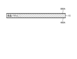
- FIG. 8 is a schematic diagram showing an example of attaching the temperature sensor 400 to the liquid crystal panel 1.
- the adhesive layer 399 is a sheet-like translucent optical member having double-sided adhesiveness such as OCA (Optical Clear Adhesive). Note that the attachment of the temperature sensor 400 to the liquid crystal panel 1 is not limited to the adhesive layer 399, and may be attached using an adhesive, for example.
- FIG. 9 is a schematic diagram showing a configuration example of a temperature sensor 400A provided integrally with the liquid crystal panel 1A.
- the liquid crystal panel 1A integrally provided with the function of the liquid crystal panel 1 and the function of the temperature sensor 400 as shown in FIG. may In this case, temperature sensor 400A functions similarly to temperature sensor 400.
- the temperature sensor 400A is laminated on the second electrode 33 on the side of the liquid crystal layer 4 of the opposing substrate 3 via an insulating layer, for example.
- FIG. 10 is a schematic diagram showing an example of an acquisition range of temperature information on the liquid crystal panel 1.
- temperature detection area SA and partial temperature detection area PA refer to areas where temperature information is acquired by temperature sensor 400 or temperature sensor 400A.
- a part of the plate surface of the rectangular liquid crystal panel 1, and an area near one of the four corners may be used as the temperature detection area SA.
- An area covering most of the plate surface of the rectangular liquid crystal panel 1 may be used as the temperature detection area SA.
- a plurality of partial temperature detection areas PA may be arranged within the board surface of the rectangular liquid crystal panel 1 .
- the temperature sensor 400 provided as a configuration corresponding to example P4 in FIG. 10 will be described below with reference to FIG.
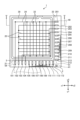
- FIG. 11 is a schematic diagram showing the main configuration and control device of the temperature sensor 400.
- the temperature sensor 400 has a sensor substrate 402 and a sensor section 403 .
- the sensor base 402 has a temperature detection area SA and a peripheral area GA.
- the temperature detection area SA includes a plurality of partial temperature detection areas PA.
- a plurality of partial temperature detection areas PA are areas in which a plurality of temperature detection resistors ER of the sensor section 403 are provided. Note that the z-direction is also the normal direction of the sensor substrate 402 .
- the temperature detection resistor ER is an electric resistance made of an alloy, a compound containing a metal (metallic compound), or a metal.
- the temperature detection resistor ER may be a laminate in which a plurality of types of materials corresponding to at least one of metals, alloys, and metallic compounds are laminated.
- alloy or the like refers to a material that can be employed as the composition of the temperature detection resistor ER and a heating resistor 811, which will be described later.
- the temperature detection resistor ER has a configuration in which a plurality of L-shaped wirings having long sides along the y direction are connected in the x direction. In this aspect, a plurality of L-shaped wirings are connected such that short sides of two L-shaped wirings adjacent in the x-direction are alternated in the y-direction to form the form of the temperature detection resistor ER. It is
- the peripheral area GA is an area between the outer circumference of the temperature detection area SA and the edge of the sensor base 402, and is an area where the temperature detection resistor ER is not provided.
- a plurality of reference resistance elements 401 are provided in the peripheral area GA.
- a temperature sensor is composed of the temperature detection resistor ER provided in the partial temperature detection area PA and the reference resistance element 401 provided in the peripheral area GA.
- the temperature detection resistor ER and the reference resistance element 401 are connected to wiring provided on the FPC 54 .
- Wiring included in the FPC 54 is connected to the system board 60 .
- the wiring provided on the FPC 54 includes a ground potential line GND, a signal input line Vin, and a signal output line Vout.
- a plurality of signal output lines are provided corresponding to the number of temperature detection resistors ER, such as signal output lines Vout(1), Vout(2), . . . , Vout(15). encompasses
- a ground potential line GND shown in FIG. 11 is connected to one end of the temperature detection resistor ER.
- a ground potential line GND applies a ground potential to the temperature detection resistor ER.
- a signal input line Vin is connected to one end of the reference resistance element 401 .
- the signal output line Vout is connected to the other end of the temperature detection resistor ER and the other end of the reference resistance element 401 .
- a drive signal for the temperature sensor 400 is input from the signal input line Vin.
- the drive signal is output to the signal output line Vout via the temperature sensor 400 .
- the strength of the signal output from the signal output line Vout depends on the temperature of the temperature detection resistor ER connected to the signal output line Vout. That is, the temperature of the partial temperature detection area PA provided with the temperature detection resistor ER can be detected based on the signal output from the signal output line Vout.
- the number of electrical resistance elements provided as the reference resistance element 401 and the number of signal output lines Vout correspond to the number of temperature detection resistors ER.
- the plurality of electrical resistance elements are connected in parallel to one signal input line Vin.
- the number of temperature detection resistors ER is not limited to 15, and can be changed as appropriate.
- the specific form of the temperature sensor 400, such as the wiring shape of the temperature detection resistor ER is not limited to this, and can be changed as appropriate.
- the temperature sensor provided in the lighting device 50 is the temperature sensor 400. Further, a sensor for acquiring information indicating the temperature of each part of the lighting device 50 is provided. may be As a specific example, any one of the temperature sensors 451, 452, 453, and 454 shown in FIG. 1 may be provided.
- the temperature sensor 451 is provided in the FPC 54 at a position extremely close to the light control device 700 . Since the temperature sensor 451 can function very similarly to the temperature sensor 400 described with reference to FIG. The temperature may be treated as the temperature of the liquid crystal panel 1 of the light control device 700 .
- the temperature sensor 452 is provided at a position in contact with or close to the light source 52 .
- the temperature sensor 453 is provided at a position in contact with or close to the circuit provided on the system board 60 .
- a temperature sensor 454 is provided in the housing 51 .
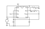
- FIG. 12 is a diagram showing a voltage dividing circuit composed of the temperature detection resistor ER and the reference resistor element 401.
- FIG. The temperature detection resistor ER and the reference resistance element 401 described with reference to FIG. 11 constitute a voltage dividing circuit as shown in FIG.
- the signal output lines Vout(1), Vout(2), . . . , Vout(15) described above can be regarded as output lines of the voltage dividing circuit. Since the electrical resistance value of the reference resistance element 401 is fixed, the output from the signal output line Vout(k) of the voltage dividing circuit depends on the electrical resistance value of the temperature detection resistor ER functioning as a variable resistor.
- the electrical resistance value of the temperature detection resistor ER corresponds to the temperature of the temperature detection resistor ER.
- the magnitude of the output from the signal output line Vout(k) corresponds to the temperature at the location where the temperature detection resistor ER is provided. Accordingly, by providing the temperature sensor 400 including the temperature detection resistor ER in the liquid crystal panel 1, information regarding the temperature at the location where the temperature detection resistor ER is provided can be obtained based on the output from the signal output line Vout(k). can get.
- k is any natural number equal to or less than j.
- the term "voltage dividing circuit described with reference to FIG. 12" includes the reference resistance element 401 and the temperature detecting resistor ER, and the output is a divided voltage corresponding to the temperature of the temperature detecting resistor ER. Point to the circuit.
- FIG. 13 is a graph showing an example of the relationship between the temperature of the temperature detection resistor ER in the voltage dividing circuit described with reference to FIG. 12 and the voltage of the electrical signal obtained as the output of the voltage dividing circuit.
- the electrical resistance value on the ground (GND) side of the voltage dividing circuit described with reference to FIG. 12 increases, and the output voltage of the voltage dividing circuit increases.
- the analog signal output from the signal output line Vout (k) is converted into a digital signal, and the temperature indicated by the digital signal is derived by software processing or circuit logic based on an algorithm similar to the software processing. Processing is performed by circuitry provided on the integrated circuit.
- a configuration for converting an analog signal into a digital signal and the integrated circuit may be the same (for example, an MCU 62 to be described later) or may be separate.
- the configuration of the temperature sensor 400 corresponding to the example P4 of FIG. 10 has been described.
- ER temperature detection resistor
- the partial temperature detection area PA temperature detection resistor ER
- the sensor substrate 402 of the temperature sensor 400 shown in FIG. 11 is replaced with the substrate of the liquid crystal panel 1 (for example, the opposing substrate 3).
- the output from the signal output line Vout(k) is transmitted to the circuit provided on the system board 60 via the FPC 54 .
- a circuit provided on the system board 60 performs temperature rise suppression control. Temperature rise suppression control is operation control of the illumination device 50 that is performed to suppress a further rise in the temperature of the liquid crystal panel 1 .
- a multiplexer may be provided on the signal output path from the signal output line Vout(j).
- the configuration for example, the circuit provided on the system board 60
- the configuration that receives the output from the signal output line Vout(k) can reduce the number of terminals for receiving the output.
- the signal output line Vout(j) and the configuration may be individually connected.
- the temperature of the light control device 700 decreases due to the environment. can be detected more quickly by the temperature sensor 400 .
- the temperature sensor 400 may be provided as the second configuration 906 instead of the first configuration 905 .
- the temperature rise of the light control device 700 which may rise due to the radiation heat from the component provided on the z2 direction side with respect to the light control device 700, is Sensor 400 facilitates faster detection.
- the configuration provided on the z2 direction side with respect to the light control device 700 refers to the light source 52 and the circuits provided on the system board 60, which will be described later.
- the heating unit 800 is provided as the first component 905 .
- the first configuration 905 is the heating unit 800, in an environment where the outside air of the lighting device 50 is low enough to affect the operation of the light control device 700 (for example, less than a predetermined temperature described later), the influence Among the plurality of liquid crystal panels 1 included in the light control device 700, the z1 direction side of the liquid crystal panel 1 positioned closest to the z1 direction side, which receives a relatively large amount of heat, can be heated more quickly.
- the heating unit 800 is provided as the second configuration 906, for example.
- the second structure 906 is the heating unit 800, intensive and rapid heating including the effect of heating the light control device 700 by radiant heat from the structure provided on the z2 direction side with respect to the light control device 700 is performed. can do
- FIG. 14 is a schematic diagram showing an arrangement example of the heating area HA and the partial heating area HPA with respect to the liquid crystal panel 1.
- the heating range HA and the partial heating range HPA refer to the range in which the heating resistor 811 of the heating unit 800 or the heating resistor 811 of the heating unit 801 is provided.
- a portion of the plate surface of the rectangular liquid crystal panel 1, and an area near one of the four corners may be set as the heating range HA.
- a region covering most of the plate surface of the shaped liquid crystal panel 1 may be set as the heating range HA.
- a plurality of partial heating areas HPA may be arranged within the plate surface of the rectangular liquid crystal panel 1 .
- the partial heating range HPA provided as a configuration corresponding to example P7 in FIG. 14 will be described below with reference to FIG.
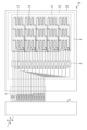
- FIG. 15 is a schematic diagram showing a heating resistor 811 provided in the partial heating area HPA and a configuration connected to the heating resistor 811.
- the heating resistor 811 is an electrical resistor made of an alloy or the like.
- the heating resistor 811 has a form in which a plurality of L-shaped wirings with long sides along the y direction are connected in the x direction.
- the heating resistor 811 is formed by connecting a plurality of L-shaped wirings such that the short sides of two L-shaped wirings adjacent in the x direction are alternated in the y direction.
- the wiring 812 is individually provided for each heating resistor 811 and connected to one end of the wiring of each heating resistor 811 .
- the wiring 813 is connected to the other ends of the wirings of the plurality of heating resistors 811 .
- the wiring 812 and the wiring 813 are not directly connected, but connected via the heating resistor 811 .
- the wiring 812 and the wiring 813 are formed in different wiring layers stacked with an insulating layer interposed therebetween.
- the heating resistor 811 may be formed in the same layer as either one of the wiring 812 and the wiring 813, or may be formed in a layer different from the wiring 812 and the wiring 813.
- the heating unit 801 can be employed instead of the heating unit 800.
- the heating unit 801 includes a heating resistor 811, wiring 812, and wiring 814.
- the wiring 814 is individually provided for each heating resistor 811 and connected to the other end of the wiring of each heating resistor 811 .
- the wiring 812 is connected to either the anode or the cathode of the power supply.
- the wiring 813 and the wiring 814 are connected to the other of the anode or cathode of the power supply.
- the configuration corresponding to example P7 in FIG. 14 has been described.
- the heating range HA has the same configuration as one partial heating range HPA.
- FIG. 16 Next, a specific example of providing the heating unit 800 in the liquid crystal panel 1 will be described with reference to FIGS. 16 to 22.
- FIG. 16
- FIG. 16 is a schematic diagram showing an example of attaching the heating unit 800 to the liquid crystal panel 1.
- the liquid crystal panel 1 and the heating section 800 are bonded via an adhesive layer 399, for example.
- the attachment of the heating unit 800 to the liquid crystal panel 1 is not limited to the adhesive layer 399, and may be attached using an adhesive, for example.
- FIG. 17 is a schematic diagram showing a configuration example of a heating section 800A provided integrally with the liquid crystal panel 1B.
- the heating section 800A functions similarly to the heating section 800.
- the heating unit 800A has a heating resistor 811, a wiring 812, and a wiring 813 or 814, which are laminated on the second electrode 33 via an insulating layer, for example, on the liquid crystal layer 4 side of the opposing substrate 3.
- FIG. 18 is a schematic diagram showing a configuration example when the liquid crystal panel 1 is provided with the temperature sensor 400 and the heating section 800.
- a heating unit 800 may be provided on one side of the plate surface of the liquid crystal panel 1, and a temperature sensor 400 may be provided on the other side.
- An adhesive layer 399 A is interposed between the liquid crystal panel 1 and the heating section 800 .
- An adhesive layer 399 B is interposed between the liquid crystal panel 1 and the temperature sensor 400 .
- the adhesive layers 399A and 399B have the same configuration as the adhesive layer 399 described above.
- FIG. 19 is a schematic diagram showing a liquid crystal panel 1C in which the function of the liquid crystal panel 1, the function of the temperature sensor 400, and the function of the heating section 800 are integrally provided.
- the temperature sensor 400A described with reference to FIGS. 9 to 12 is provided on one side of the liquid crystal panel 1, and the heating unit 800A described with reference to FIGS. It may be provided on the other side of the panel 1 .
- the temperature sensor 400A may be formed on the opposing substrate 3 or may be formed on the array substrate 2 as described with reference to FIG.
- the temperature sensor 400A may be laminated with the first electrode 25 or the second electrode 33 via an insulating layer, for example, on the liquid crystal layer 4 side, or may It may be formed on the plate surface opposite to the plate surface facing the liquid crystal layer 4 .
- the heating portion 800A is formed on the other of the array substrate 2 and the counter substrate 3 on which the temperature sensor 400A is not formed.
- the heating part 800A may be laminated with the first electrode 25 or the second electrode 33 via an insulating layer, for example, or may be stacked on the other plate surface of the array substrate 2 or the counter substrate 3 facing the liquid crystal layer 4. may be formed on the plate surface on the opposite side of the .
- FIG. 20 is a schematic diagram showing a liquid crystal panel 1D in which the function of the liquid crystal panel 1, the function of the temperature sensor 400, and the function of the heating section 800 are integrally provided.
- the partial temperature detection area PA described with reference to FIGS. 10 and 11 and the partial temperature detection area PA described with reference to FIGS. and the partial heating range HPA described above may be alternately arranged.
- the partial temperature detection area PA and the partial heating area HPA can be provided on one surface side of the liquid crystal panel 1D.
- the temperature detection resistor ER (see FIG. 11) may be used as the heating resistor 811 (see FIG. 15).
- the detection period during which the temperature of the liquid crystal panel 1 is detected based on the electrical resistance value of the temperature detection resistor ER and the temperature detection resistor ER are supplied with power when heating is required.
- a so-called time-division control is performed in which a heating period in which the liquid crystal panel 1 is heated by the heat generated by the ER alternately occurs temporally. Note that power is supplied to the temperature detection resistor ER during the heating period when heating is required. That is, when heating is unnecessary, power is not supplied to the temperature detection resistor ER during the heating period.
- the determination as to whether or not heating is necessary is performed, for example, based on a predetermined temperature threshold. Specifically, when the temperature of the liquid crystal panel 1 detected during the detection period is equal to or lower than the temperature threshold, it is determined that heating is necessary, and otherwise, it is determined that heating is unnecessary.
- Various processes related to determination are performed by a circuit provided on the system board 60, for example.
- FIG. 21 is a schematic diagram showing a configuration in which the temperature sensor 400 in FIG. 8 is replaced with a temperature sensor/heating unit 900.
- the temperature sensor/heating unit 900 is configured such that the temperature detection resistor ER (see FIG. 11) of the temperature sensor 400 can be used as the heating resistor 811 (see FIG. 15) of the heating unit 800.
- FIG. Specifically, a closed circuit including the temperature detection resistor ER is provided so as to be switchable between a first path including the reference resistance element 401 and a second path not including the reference resistance element 401 .
- the closed circuit when the first path is established functions as the voltage dividing circuit described with reference to FIG.
- the temperature detection resistor ER In the closed circuit when the second circuit is established, the temperature detection resistor ER is connected to the wiring 812 and the wiring 813 or 814 in the same manner as the heating resistor 811 described with reference to FIG. , and the temperature detection resistor ER generates heat by applying a current to the temperature detection resistor ER and functions in the same manner as the heating resistor 811 .
- FIG. 22 is a schematic diagram showing a configuration in which the temperature sensor 400A in FIG. 9 is replaced with a temperature sensor/heating unit 900A.
- the function of the liquid crystal panel 1 and the function of the temperature sensor/heating unit 900 are integrally provided as shown in FIG.
- the liquid crystal panel 1 ⁇ /b>E may be provided in the light control device 700 .
- the temperature sensor/heating unit 900A functions in the same manner as the temperature sensor/heating unit 900 does.
- the temperature sensor/heating unit 900A is formed on the array substrate 2 or the counter substrate 3 in the same manner as the temperature sensor 400A described above.
- the configuration for heating the lighting device 50 is not limited to these.
- at least one of the heating units 851 and 852 in FIG. 1 may be further provided.
- the heating unit 851 is provided at a position in contact with or close to the light control device 700 on the side of the light control device 700 that does not face the plate surface.
- the heating part 852 is provided at a position that contacts or is close to the system board 60 .
- the temperature of the light control device 700 can easily be adjusted to a temperature more suitable for the operation of the light control device 700. Become.
- the heating unit 852 can heat the circuit. , the temperature is more likely to be suitable for the operation of the circuit.
- the first configuration 905 is provided on the liquid crystal panel 1 closest to the z1 direction among the liquid crystal panels 1 of the light control device 700 .
- the second configuration 906 is provided on the liquid crystal panel 1 closest to the z2 direction among the liquid crystal panels 1 included in the light control device 700 .
- FIG. 23 is a block diagram showing a main configuration example of the system board 60.
- the system board 60 includes, for example, a communication unit 61, an MCU (Micro Controller Unit) 62, an FPGA (Field Programmable Gate Array) 63, a D (Digital)/A (Analog) conversion unit 64, and a light source drive unit 65. and a connecting portion 66 are provided.
- the communication unit 61 communicates with the external information processing device 300 .
- the communication unit 61 has, for example, a circuit that functions as a NIC (Network Interface Controller).
- the communication unit 61 receives a signal including a command regarding the operation of the lighting device 50 transmitted from the information processing device 300 and outputs information indicating the command to the MCU 62 .
- the information processing device 300 is, for example, a mobile terminal such as a smart phone, but is not limited to this.
- the information processing device 300 may be a stationary information processing device such as a server or a PC (Personal Computer) provided for controlling the lighting device 50, or information in another form not illustrated here. It may be a processing device.
- the command related to the operation of the lighting device 50 transmitted from the information processing device 300 is, for example, a command specifying ON/OFF of light irradiation by the lighting device 50, a light irradiation range, a light intensity, and the like. , and any items that can be specified individually within the operation control range of the lighting device 50 can be included in the command.
- the MCU 62 outputs various signals to the FPGA 63 , the light source drive section 65 and the connection section 66 in accordance with the command regarding the operation of the lighting device 50 obtained from the information processing device 300 via the communication section 61 . That is, the MCU 62 controls various components of the lighting device 50 so that the lighting device 50 operates according to the operation from the information processing device 300 .
- the MCU 62 acquires the output from the signal output line Vout(k), and when the output indicates that the temperature of the liquid crystal panel 1 has reached or exceeded a predetermined temperature, the MCU 62 performs temperature rise suppression control. .
- the MCU 62 also controls the operation of the heater HEA.
- the heater HEA is, for example, the heating unit 800, but is not limited to this, and may be any one or more of the heating units 800A, 851, 852, or the partial heating unit described with reference to FIG. It may be the range HPA, or it may be the temperature sensor/heating unit 900 or the temperature sensor/heating unit 900A described with reference to FIGS. Alternatively, a heater may be provided in the heat radiation part 55 to apply heat to the light control device 700 from the heat radiation part 55 .
- the FPGA 63 performs information processing for controlling the operation of the light control device 700 under the control of the MCU 62 and outputs a signal indicating the result of the information processing to the D/A converter 64 . For example, if the instruction regarding the operation of the lighting device 50 transmitted from the information processing device 300 includes a designation regarding the irradiation range of light, the FPGA 63 adjusts the light so that the irradiation range corresponding to the designation is irradiated with light. Information processing for operating the device 700 is performed.
- the D/A conversion unit 64 is configured to output analog signals for operating the plurality of liquid crystal panels 1 included in the light control device 700 based on the digital signals from the FPGA 63 .
- the configuration may consist of one circuit or may include multiple circuits.
- the light source drive unit 65 is a controller that performs ON/OFF control of the light source unit 52 and light emission intensity control when the light source unit 52 is ON under the control of the MCU 62 .
- the controller may be a single circuit or may include multiple circuits.
- connection unit 66 is an interface that connects the MCU 62 and the input/output of the temperature sensor SEN (the ground potential line GND, the signal input line Vin, and the signal output line Vout described above). Also, the connecting portion 66 is connected to the MCU 62 and intervenes in the signal transmission path between the MCU 62 and the temperature sensor SEN.
- the temperature sensor SEN is, for example, the temperature sensor 400, but is not limited to this, and may be any one or more of the temperature sensors 400A, 451, 452, 453, and 454. See FIG. It may be the partial temperature detection area PA described above, or the temperature sensor/heating unit 900 described with reference to FIGS. 19 and 20 .
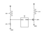
- FIG. 24 is a diagram showing a main circuit configuration example when linking the direct current flowing to the heating resistor and temperature measurement.
- MCU 62 is connected to the voltage dividing circuit and switch SW1 described with reference to FIG.
- the output of the voltage dividing circuit described with reference to FIG. 12 is input to the MCU 62 as an analog signal indicating the temperature of the temperature detection resistor ER.
- the analog signal is converted into a digital signal via an A/D converter (ADC: Analog Digital Converter) that the MCU 62 has.
- ADC Analog Digital Converter
- the MCU 62 outputs a PWM (Pulse Width Modulation) signal corresponding to the temperature of the temperature detection resistor ER indicated by the digital signal to the switch SW1.
- PWM Pulse Width Modulation
- the switch SW1 is a switching element provided on the DC current path in which the heating resistor 811 is provided.
- the switch SW1 opens and closes the DC current path according to the PWM signal. Thereby, the degree of heat generation by the heating resistor 811 is controlled.
- the switch SW1 is, for example, a MOSFET (Metal Oxide Semiconductor Field Effect Transistor), but may be another element that functions similarly.
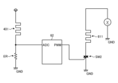
- FIG. 25 is a diagram showing a main circuit configuration example in the case of linking the AC current flowing through the heating resistor and the temperature measurement.
- MCU 62 is connected to the voltage dividing circuit and switch SW2 described with reference to FIG.
- the MCU 62 outputs a PWM signal corresponding to the temperature of the temperature detection resistor ER indicated by the digital signal to the switch SW2.
- the switch SW2 is provided on the alternating current path in which the heating resistor 811 is provided.
- the switch SW2 opens and closes the AC current path according to the PWM signal. Thereby, the degree of heat generation by the heating resistor 811 is controlled.
- the switch SW2 is, for example, a bidirectional thyristor such as a TRIAC (TRIode AC switch), but may be another element that functions similarly.
- TRIAC TRIode AC switch
- the configuration described with reference to FIG. 25 is the same as the configuration described with reference to FIG. 24, except for the items noted above.
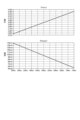
- FIG. 26 is a graph showing an example of the relationship between the pulse width of the PWM signal and the voltage applied to the heating resistor 811.
- FIG. 26 the voltage per unit time applied to the heating resistor 811 rises and falls according to the duty ratio of the PWM signal given from the MCU 62 to the switch SW1 or switch SW2. As the period during which the output of the PWM signal is not 0 increases within the unit time, the voltage applied to the heating resistor 811 increases within the unit time, and the degree of heat generation by the heating resistor 811 increases.
- FIG. 27 is a diagram showing a circuit configuration example that employs a digital potentiometer as a configuration for controlling the amount of heat generated by the heating resistor 811.
- FIG. When the switch SW3, which is a digital potentiometer, is employed in place of the switch SW1 in the configuration described with reference to FIG. A signal (control signal) for controlling the resistance value is output to the switch SW3.
- the switch SW3 causes an electrical resistance value corresponding to the control signal to be generated on the DC current path provided with the heating resistor 811 . Thereby, the degree of heat generation by the heating resistor 811 is controlled.
- the configuration described with reference to FIG. 27 is the same as the configuration described with reference to FIG. 24, except for the items noted above.
- FIG. 28 is a graph showing the relationship in which the current flowing through the heater decreases as the potential of the portion divided by the digital potentiometer and heater increases.
- the degree of heat generation by the heating resistor 811 increases.
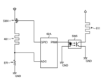
- FIG. 29 is a diagram showing a circuit configuration example in which power consumption is reduced by adding ON/OFF circuits for the temperature sensor and the heater individually and turning each ON/OFF.
- the MCU 62A shown in FIG. 29 has a GPIO (General Purpose Input/Output) input/output function in addition to the functions of the configuration of the MCU 62 described with reference to FIG. In the configuration shown in FIG. 29, the GPIO is used as a port for controlling the operation of switch SW4.
- GPIO General Purpose Input/Output
- the switch SW4 is a load switch IC (Integrated Circuit) provided between the reference resistance element 401 in the voltage dividing circuit described with reference to FIG. 12 and the power supply of the voltage dividing circuit.
- the MCU 62A controls ON/OFF of the voltage dividing circuit described with reference to FIG. 12 by controlling ON/OFF of the switch SW4. For example, when the time-division control described above is performed, operation control is adopted in which the voltage dividing circuit is turned on during the detection period and turned off during the heating period.
- a switch SW5 is adopted instead of the switch SW1.
- the switch SW5 is a photocoupler.
- the switch SW5 opens and closes the AC current path provided with the heating resistor 811 according to the duty ratio of the PWM signal given from the MCU 62, like the switch SW1.
- the configuration described with reference to FIG. 29 is the same as the configuration described with reference to FIG. 24, except for the items noted above.
- FIG. 30 is a diagram showing a circuit configuration example for converting the output of the voltage dividing circuit into a pulse wave.
- the timer IC 621 shown in FIG. 30 converts the output of the voltage dividing circuit described with reference to FIG. 12 obtained from the input terminal Disc into a pulse wave and outputs it from the output terminal Out.
- the frequency of the pulse wave corresponds to the magnitude of the output of the voltage dividing circuit described with reference to FIG. Specifically, when the temperature of the temperature detection resistor ER is higher, the electrical resistance value of the temperature detection resistor ER is increased. The higher the electrical resistance value of the temperature detection resistor ER, the lower the frequency of the pulse wave.
- the ADC can be omitted from the MCU 62. That is, by providing a timer IC 621 between the voltage dividing circuit described with reference to FIG.
- the pulse wave output from the timer IC 621 is, for example, a rectangular wave, but may be another pulse wave that can be used as a digital signal.
- FIG. 31 shows a circuit configuration example for controlling the magnitude of the current flowing through the heating resistor 811 according to the output of the voltage dividing circuit described with reference to FIG. 12 without using an MCU such as the MCU 62. It is a diagram.
- a comparator COMP is provided as a configuration for receiving the output of the voltage dividing circuit described with reference to FIG. Comparator COMP provides switch SW6 with an output corresponding to the result of comparison between the output of the voltage dividing circuit described with reference to FIG. 12 and the output of setting circuit SET indicating a predetermined electrical resistance value.
- the switch SW6 opens and closes the alternating current path provided with the heating resistor 811 according to the output of the comparator COMP.
- the configuration described with reference to FIG. 31 is the same as the configuration described with reference to FIG. 24, except for the items noted above.
- Fig. 32 is a graph showing the heater OFF when the temperature sensor reaches 25°C, and is a graph showing a series of operations when SET in Fig. 31 is set to 1V.
- the comparator COMP opens and closes the switch SW6 according to the comparison result between the output voltage and the output voltage of the setting circuit SET. In FIG. 32, when the temperature of the temperature detection resistor ER is 25° C.
- the threshold Thr for switching ON/OFF of the current to the heating resistor 811 is 25° C., but the threshold Thr depends on the output voltage of the setting circuit SET and can be set to any temperature. can.
- FIG. 33 is a diagram showing an example of realizing precise resistance value measurement by detecting the potential difference between both ends of the temperature detection resistor ER in measurement using a differential amplifier circuit.
- a differential amplifier that produces an output corresponding to the difference between the output voltage of the voltage dividing circuit described with reference to FIG. 12 and the voltage on the ground (GND) side of the voltage dividing circuit.
- DifA is provided.
- the heating resistor 811 can generate heat according to the output of the voltage dividing circuit described with reference to FIG.
- FIG. 34 is a graph showing an example of the relationship between the temperature of the temperature detection resistor ER, the output voltage of the voltage dividing circuit described with reference to FIG. 12, the sensor output, and the heater input. It should be noted that the sensor output in FIG. 34 refers to the current generated according to the difference between the voltage on the ground (GND) side of the voltage dividing circuit. A heater input indicates a current flowing through the heating resistor 811 . As shown in FIG. 34, as the temperature rises, the sensor output increases and the heater input decreases.
- the configuration may be the FPGA 63, the MCU 62, or a dedicated configuration (not shown).
- FIG. 35 is a flowchart showing the processing flow of the operation of the lighting device 50.
- step S1 each component provided on the system board 60 performs an initial operation (step S2).
- step S2 the MCU 62 performs processing corresponding to the operation mode so that the illumination device 50 operates in the operation mode (emission intensity, light distribution range, etc.) specified by the signal transmitted from the information processing device 300.
- the FPGA 63 , the light source driving section 65 and the like start operating under the operation control of the MCU 62 .
- step S3 the light control device 700 operates (step S3), and the light transmittance of the light control device 700 is controlled so that the light distribution range specified by the operation mode described above is irradiated with light. .
- step S3 the light source 52 is turned on (step S4).
- step S5 temperature measurement is performed (step S5).
- the MCU 62 operates the temperature sensor 400 and obtains information about the temperature of the liquid crystal panel 1 by obtaining an output from the signal output line Vout(k). Data indicating the correspondence relationship between the magnitude of the output from the signal output line Vout(k) and the temperature of the liquid crystal panel 1 provided with the temperature sensor 400 is obtained in advance by experiment or the like.
- the MCU 62 determines whether a temperature lower than the predetermined temperature is measured in the process of step S5 (step S6). When the temperature below the predetermined temperature is measured (step S6; Yes), the MCU 62 performs heat treatment (step S7).
- FIG. 36 is a flow chart showing the flow of the heat treatment (step S7) in FIG.
- step S7 the temperature of ⁇ 20° C. or less is measured in the process of step S5 described above (step S11; Yes)
- the MCU 62 turns off the operation of the light control device 700 (step S12).
- the heating resistor 811 is driven at a predetermined maximum heat generating capacity (100%) (step S13).
- a state in which the heating resistor 811 is driven with a predetermined maximum heat generation capacity (100%) means a state in which the maximum current within the range of current allowed by the heating resistor 811 is applied to the heating resistor 811 .
- step S5 if the temperature of -20°C or lower is not measured (step S11; No), the MCU 62 turns on the operation of the light control device 700 (step S14). In addition, according to a predetermined heater operation setting (step S15), the heater is driven according to the heater operation setting (step S16).
- FIG. 37 is a diagram showing an example of predetermined heater operation settings described as the operation of step S15.
- ⁇ 20° C. or less is measured as the temperature of the temperature detection resistor ER, it is driven at a predetermined maximum heat generation capacity (100%), and when ⁇ 20° C. or higher and ⁇ 10° C. or less is measured. is driven at 75% of the predetermined maximum heat generation capacity when the 30% of the maximum predetermined heat generation capacity when measured above 0°C and below 0°C, and 10% of the maximum predetermined heat generation capacity when measured above 0°C and below 10°C. % driven settings are shown.
- the heater operation setting described with reference to FIG. 37 is merely an example and is not limited to this, and can be changed as appropriate.
- step S7 After the heating process (step S7) shown in FIG. 35, unless the lighting device 50 is powered off (step S8; No), the process proceeds to step S5 again.
- step S8; Yes When the lighting device 50 is powered off (step S8; Yes), the operation of the lighting device 50 ends. Also, in the process of step S5, when the temperature below the predetermined temperature is not measured (step S6; No), the process of step S7 is not performed and the process proceeds to the branch of step S8.
- the specific form of the lighting device is not limited to that shown in FIG.
- the lighting device 50A shown in FIG. 38 or the lighting device 50B shown in FIG. 39 may be used.
- FIG. 38 is a schematic diagram showing the main configuration of the illumination device 50A.
- the illumination device 50A includes a third configuration 907 and a fourth configuration 908 instead of the first configuration 905 and the second configuration 906 included in the illumination device 50 described with reference to FIG.
- the third configuration 907 is provided on the opposite side (z1 direction side) of the reflector 53 with respect to the light control device 700 .
- the fourth structure 908 is provided on the z1 direction side with respect to the third structure 907 .
- One of the third configuration 907 and the fourth configuration 908 may be the temperature sensor 400 and the other may be the heating unit 800, but at least one of the third configuration 907 and the fourth configuration 908 may be the other. may be configured.
- Other configurations include, for example, a polarizing plate or a light control mirror.
- a polarizing plate transmits light polarized in a specific direction and blocks light polarized in other directions.
- the polarization direction of light that can pass through the polarizing plate can be arbitrarily determined at the time of design. By shielding part of the light with the polarizing plate, heating by the infrared rays contained in the light can be expected.
- the light control mirror has a structure in which a structure in which the liquid crystal layer in the liquid crystal display panel is an electrochromic layer and a half mirror are laminated.
- the electrochromic layer includes a thin film of electrochromic material such as WO3, NbO5, TiO2, and an electrolyte solution.
- the dimmer mirror has the effect of suppressing yellowing of light and obtaining visibility toward blue.
- the half mirror of the light control mirror is provided so as to reflect part of the light traveling from the z2 direction side to the z1 direction side to the z2 direction side. Heating of the liquid crystal panel 1 by the infrared rays contained in the reflected light can be expected by the light control mirror.
- One of the third structure 907 and the fourth structure 908 is one of the polarizing plate and the light control mirror, and the other of the third structure 907 and the fourth structure 908 is the other of the polarizing plate and the light control mirror.
- a configuration having a heater function may be the third configuration 907, and the polarizing plate or the light control mirror may be the fourth configuration 908. good too.
- the second configuration 906 shown in FIG. may be used as the temperature sensor 400 .
- FIG. 39 is a schematic diagram showing the main configuration of the illumination device 50B.
- the lighting device 50B includes a plurality of light sources.
- FIG. 39 illustrates an illumination device 50B including two light sources 52A and 52B, the illumination device may be provided with three or more light sources.
- the lighting device provided with a plurality of light sources also has a temperature sensor (for example, the temperature sensor 400, etc.) in the same manner as the lighting device 50 described with reference to FIG.
- a temperature sensor for example, the temperature sensor 400, etc.
- the temperature sensor detects a temperature below a predetermined temperature (for example, below 10° C.)
- the plurality of light sources are turned on.
- a predetermined temperature for example, below 10° C.
- a predetermined temperature for example, below 10° C.
- the temperature sensor detects a temperature equal to or higher than a predetermined temperature for example, 10° C. or higher
- a predetermined temperature for example, 10° C. or higher
- the illumination device for example, the illumination devices 50, 50A, and 50B
- the illumination device includes a light source (light source 52) that emits light and at least one liquid crystal panel (liquid crystal panel) on the light emitting side of the light source. It has a panel 1), and adjusts the light distribution range of the light emitted from the liquid crystal panel to the outside by controlling the transmittance of light passing through the liquid crystal panel and the transmission range of light passing through the liquid crystal panel.
- a light control device (light control device 700), a temperature sensor (temperature sensor 400, partial temperature detection area PA or temperature sensor/heating unit 900, 900A) for acquiring information indicating the temperature of the liquid crystal panel, and the liquid crystal panel
- the heating unit (heating unit 800, 801, 800A, temperature sensor/heating unit 900, 900A, partial heating range HPA or multiple light sources) and the temperature sensor obtained information indicating a temperature below a predetermined temperature and a control unit (MCUs 62 and 62A, timer IC 621, comparator COMP or differential amplifier DifA) that operates the heating unit in the case. Therefore, the heating unit can suppress the temperature drop of the liquid crystal panel provided on the emission path of the light from the light source, which is included in the light control device.
- the heating unit since the heating unit is operated when the temperature sensor acquires information indicating a temperature equal to or lower than the predetermined temperature, the heating unit can be appropriately operated when the liquid crystal panel needs to be heated.
- the heating unit (temperature sensor/heating unit 900, 900A or partial heating area HPA) is a heater having a first lead wire unit (heating resistor 811) that generates heat in response to power supply, the liquid crystal panel (liquid crystal panel 1 ) is extremely easy, and the liquid crystal panel can be preferably heated.
- the temperature sensor (temperature sensor 400) has a second conducting wire portion (temperature detecting resistor ER) whose electric resistance value changes with temperature, and the first conducting wire portion (heating resistor 811) and the second conducting wire portion are provided on the same surface of the liquid crystal panel (liquid crystal panel 1) (see, for example, FIGS. 20 to 22).
- a second conducting wire portion temperature detecting resistor ER
- the first conducting wire portion heating resistor 811
- the second conducting wire portion are provided on the same surface of the liquid crystal panel (liquid crystal panel 1) (see, for example, FIGS. 20 to 22).
- the heating unit also supplies power to the second conductor (temperature detection resistor ER) to cause the second conductor to generate heat. As a result, attenuation of light from the light source (light source 52) due to the conducting wire can be further reduced.
- the lighting device (for example, the lighting device 50B) reflects part of the light that has passed through the light control device (light control device 700) from the light source (light source 52 or one of the light sources 52A and 52B) toward the light source side. Equipped with a part (light control mirror). This makes it possible to increase the number of heat sources for heating the light control device.
- the illumination device for example, illumination device 50B
- the light control device includes a polarizing plate that transmits light in a specific polarization direction and blocks light in other polarization directions. This makes it possible to increase the number of heat sources for heating the light control device.
- a plurality of light sources (for example, the light sources 52A and 52B) are provided, and one or more of the plurality of light sources is operated as a heating unit. and the operation for heating the lighting device.
- the specific structure of the light control device 700 is not limited to the example described with reference to FIG.
- the light control device 700 may have a liquid crystal panel functioning as a so-called liquid crystal lens, which is provided so as to be able to change the degree of refraction of light directed from one side to the other side by controlling the light distribution of the liquid crystal. good.
Abstract
This lighting device is provided with: a light source that emits light; a dimmer device that has at least one liquid-crystal panel on the light-output side of the light source, and that controls the transmittance of light transmitted through the liquid crystal panel and the transmission range of the light transmitted through the liquid crystal panel, thereby adjusting the light distribution range of light emitted externally from the liquid crystal panel; a temperature sensor that acquires information indicating the temperature of the liquid crystal panel; a heating unit that heats the liquid crystal panel; and a control unit that causes the heating unit to operate if information that indicates a temperature below a prescribed temperature is acquired by the temperature sensor.
Description
本開示は、照明装置に関する。
The present disclosure relates to lighting devices.
装置の向きを変更可能に設けることで光の照射範囲を変更できる照明装置が知られている(例えば特許文献1)。
A lighting device is known that can change the irradiation range of light by providing the direction of the device to be changeable (for example, Patent Document 1).
特許文献1に記載の照明装置では、光源の向きを変えられるように可動部及び駆動部を設ける必要がある。このような構成では大型化を免れないうえ、照明装置の周囲に照明装置の稼働を許容する空間が必要になる。
In the lighting device described in Patent Document 1, it is necessary to provide a movable part and a driving part so that the direction of the light source can be changed. Such a configuration inevitably results in an increase in size, and requires a space around the lighting device to allow the operation of the lighting device.
そこで、光源からの光の出射経路上に液晶パネルを設け、当該液晶パネルにおける光の透過範囲と光の透過の度合いとを制御することで、照明装置を小型にしつつ、光の配光制御をより柔軟に行える。しかしながら、液晶パネルには、正常に動作する温度範囲が限定されていることから、液晶パネルの温度が当該温度範囲を逸脱した低温になった場合を想定した対策が必要になる。
Therefore, by providing a liquid crystal panel on the output path of the light from the light source and controlling the light transmission range and the degree of light transmission in the liquid crystal panel, the lighting device can be made compact and the light distribution can be controlled. be more flexible. However, since the liquid crystal panel has a limited temperature range in which it can operate normally, it is necessary to take countermeasures assuming that the temperature of the liquid crystal panel falls outside that temperature range.
本開示は、上記の課題に鑑みてなされたもので、光源からの光の出射経路上に設けられた液晶パネルの温度低下を抑制できる照明装置を提供することを目的とする。
The present disclosure has been made in view of the above problems, and an object thereof is to provide a lighting device capable of suppressing a temperature drop of a liquid crystal panel provided on an emission path of light from a light source.
本開示の一態様による照明装置は、光を発する光源と、前記光源の出光側に少なくとも1つの液晶パネルを有し、前記液晶パネルを透過する光の透過率及び前記液晶パネルを透過する光の透過範囲をそれぞれ制御することで前記液晶パネルから外部に照射される光の配光範囲を調節する調光装置と、前記液晶パネルの温度を示す情報を取得する温度センサと、前記液晶パネルを加熱する加熱部と、前記温度センサで所定温度以下の温度を示す情報が得られた場合に前記加熱部を動作させる制御部と、を備える。
A lighting device according to an aspect of the present disclosure includes a light source that emits light and at least one liquid crystal panel on a light output side of the light source, and the transmittance of light passing through the liquid crystal panel and the rate of light passing through the liquid crystal panel are A light control device that adjusts the light distribution range of light emitted from the liquid crystal panel to the outside by controlling the transmission range, a temperature sensor that acquires information indicating the temperature of the liquid crystal panel, and a heater for the liquid crystal panel. and a control unit that operates the heating unit when information indicating a temperature equal to or lower than a predetermined temperature is obtained from the temperature sensor.
以下に、本開示の各実施の形態について、図面を参照しつつ説明する。なお、開示はあくまで一例にすぎず、当業者において、発明の主旨を保っての適宜変更について容易に想到し得るものについては、当然に本開示の範囲に含有されるものである。また、図面は説明をより明確にするため、実際の態様に比べ、各部の幅、厚さ、形状等について模式的に表される場合があるが、あくまで一例であって、本開示の解釈を限定するものではない。また、本明細書と各図において、既出の図に関して前述したものと同様の要素には、同一の符号を付して、詳細な説明を適宜省略することがある。
Each embodiment of the present disclosure will be described below with reference to the drawings. It should be noted that the disclosure is merely an example, and those skilled in the art can easily conceive of appropriate modifications while maintaining the gist of the invention are, of course, included in the scope of the present disclosure. In addition, in order to make the description clearer, the drawings may schematically show the width, thickness, shape, etc. of each part compared to the actual embodiment, but this is only an example, and the interpretation of the present disclosure is not intended. It is not limited. In addition, in this specification and each figure, the same reference numerals may be given to the same elements as those described above with respect to the existing figures, and detailed description thereof may be omitted as appropriate.
図1は、照明装置50の主要構成を示す模式図である。照明装置50は、筐体51と、光源52と、リフレクター53と、調光装置700と、FPC(Flexible Printed Circuits)54と、システム基板60と、放熱部55と、を備える。筐体51は、光源52と、リフレクター53と、調光装置700と、FPC54と、システム基板60と、放熱部55と、を収める筐体である。筐体51は、放熱性に優れた素材(例えば、アルミニウム等)で構成されることが望ましい。
FIG. 1 is a schematic diagram showing the main configuration of the illumination device 50. FIG. The lighting device 50 includes a housing 51 , a light source 52 , a reflector 53 , a light control device 700 , an FPC (Flexible Printed Circuits) 54 , a system board 60 and a heat dissipation section 55 . The housing 51 is a housing that houses the light source 52 , the reflector 53 , the light control device 700 , the FPC 54 , the system board 60 , and the heat dissipation section 55 . The housing 51 is desirably made of a material (for example, aluminum) having excellent heat dissipation properties.
光源52は、電力供給に応じて光を発する。光源52は、例えばLED(light emitting diode)であるが、他の形態の電灯であってもよい。例えば、光源52は、白熱電球であってもよい。
The light source 52 emits light in response to power supply. The light source 52 is, for example, an LED (light emitting diode), but may be another form of electric light. For example, light source 52 may be an incandescent bulb.
リフレクター53は、光源52から発せられる光を調光装置700側へ誘導する。リフレクター53の説明に係り、リフレクター53に対して調光装置700側をz1方向側とし、リフレクター53に対して光源52側をz2方向側とする。また、z1方向とz2方向との対向方向をz方向とする。リフレクター53は、光源52が位置するz2方向側からz1方向側に向かうにつれてz方向に直交する平面視点での開口幅が末広がり状に拡大する光学部材である。リフレクター53は、プリズム等の屈折又は当該末広がり状の内周面の鏡面加工によって光源52から発せられる光を調光装置700側へ誘導する。
The reflector 53 guides the light emitted from the light source 52 to the light control device 700 side. Regarding the description of the reflector 53, the light control device 700 side of the reflector 53 is the z1 direction side, and the light source 52 side of the reflector 53 is the z2 direction side. Also, the opposite direction of the z1 direction and the z2 direction is defined as the z direction. The reflector 53 is an optical member whose opening width in a plan view orthogonal to the z-direction expands in the direction from the z2-direction side where the light source 52 is located toward the z1-direction side. The reflector 53 guides the light emitted from the light source 52 to the light control device 700 side by refraction of a prism or the like or mirror finishing of the inner peripheral surface of the divergent shape.
FPC54は、調光装置700が有する液晶パネル1に接続される配線ならびに後述する図11を参照して説明する接地電位線GND及び信号出力線Vout(j)を含む。システム基板60は、1つ以上の回路が設けられる回路基板である。放熱部55は、システム基板60に設けられた構成からの熱の放射を促す構成を含む。当該構成として、例えばヒートシンク等が挙げられる。
The FPC 54 includes wiring connected to the liquid crystal panel 1 of the light control device 700, a ground potential line GND and a signal output line Vout(j), which will be described later with reference to FIG. System board 60 is a circuit board on which one or more circuits are provided. The heat sink 55 includes a structure that facilitates heat radiation from structures provided on the system board 60 . Examples of the configuration include a heat sink and the like.
調光装置700は、光源52から発せられた光及び光源52から発せられてリフレクター53によって誘導された光の透過の度合い及び透過範囲を変更可能に設けられる。調光装置700には、第1構成905と、第2構成906と、が設けられる。第1構成905は、調光装置700のリフレクター53側(z1方向側)に設けられる。第2構成906は、調光装置700に対して第1構成905の反対側(z2方向側)に設けられる。第2構成906は、例えば温度センサ400(図10参照)である。温度センサ400は、調光装置700が有する液晶パネル1の温度に関する情報を取得する。
The light control device 700 is provided so as to be able to change the degree of transmission and transmission range of the light emitted from the light source 52 and the light emitted from the light source 52 and guided by the reflector 53 . The dimming device 700 is provided with a first configuration 905 and a second configuration 906 . The first configuration 905 is provided on the reflector 53 side (z1 direction side) of the light control device 700 . The second configuration 906 is provided on the opposite side (z2 direction side) of the first configuration 905 with respect to the light control device 700 . A second configuration 906 is, for example, a temperature sensor 400 (see FIG. 10). The temperature sensor 400 acquires information regarding the temperature of the liquid crystal panel 1 of the light control device 700 .
図2は、調光装置700の構成例を示す模式図である。図2に示すように、調光装置700は、z方向に並ぶ複数の液晶パネル1を有する。図2では、4つの液晶パネル1を有する調光装置700を示しているが、液晶パネル1の数は4つに限られるものでなく、適宜変更可能である。
FIG. 2 is a schematic diagram showing a configuration example of the light control device 700. FIG. As shown in FIG. 2, the light control device 700 has a plurality of liquid crystal panels 1 arranged in the z direction. FIG. 2 shows the light control device 700 having four liquid crystal panels 1, but the number of liquid crystal panels 1 is not limited to four and can be changed as appropriate.
次に、調光装置700に含まれる液晶パネル1について、図3から図7を参照して説明する。
Next, the liquid crystal panel 1 included in the light control device 700 will be described with reference to FIGS. 3 to 7. FIG.
図3は、実施形態に係る液晶パネル1の斜視図である。図4は、実施形態に係るアレイ基板2の配線を示す平面図であり、アレイ基板2を上側から見た図である。図5は、実施形態に係る対向基板3の配線を示す平面図であり、対向基板を上側から見た図である。図6は、実施形態に係る液晶パネル1の配線を示す平面図であり、液晶パネル1を上側から見た図である。図7は、図6のV-V線による断面図である。なお、図3から図6に示すxyz座標において、x1方向及びx2方向に沿う方向をx方向と称する。x1方向と、x2方向と、は逆である。また、y1方向及びy2方向に沿う方向をy方向と称する。y1方向と、y2方向と、は逆である。x方向とy方向とは直交する。x方向及びy方向が沿う平面と、z方向とは直交する。
FIG. 3 is a perspective view of the liquid crystal panel 1 according to the embodiment. FIG. 4 is a plan view showing wiring of the array substrate 2 according to the embodiment, and is a view of the array substrate 2 viewed from above. FIG. 5 is a plan view showing the wiring of the opposing substrate 3 according to the embodiment, and is a view of the opposing substrate viewed from above. FIG. 6 is a plan view showing wiring of the liquid crystal panel 1 according to the embodiment, and is a view of the liquid crystal panel 1 viewed from above. 7 is a cross-sectional view taken along line VV of FIG. 6. FIG. In addition, in the xyz coordinates shown in FIGS. 3 to 6, the direction along the x1 direction and the x2 direction is referred to as the x direction. The x1 direction and the x2 direction are opposite. A direction along the y1 direction and the y2 direction is referred to as the y direction. The y1 direction and the y2 direction are opposite. The x-direction and the y-direction are orthogonal. A plane along which the x-direction and the y-direction extend is orthogonal to the z-direction.
図3に示すように、液晶パネル1は、アレイ基板2と、対向基板3と、液晶層4と、シール材30と、を有する。
As shown in FIG. 3 , the liquid crystal panel 1 has an array substrate 2 , a counter substrate 3 , a liquid crystal layer 4 and a sealing material 30 .
図3および図6に示すように、アレイ基板(第1基板)2は、対向基板(第2基板)3よりも大きい。即ち、対向基板(第2基板)3の面積は、アレイ基板(第1基板)2の面積よりも小さい。アレイ基板2は、透明ガラス23(図4参照)を有する。対向基板3は、透明ガラス31(図5参照)を有する。実施形態において、アレイ基板2および対向基板3は、上側から見た平面視で正方形であるが、本発明に係る基板の形状は正方形に限定されない。アレイ基板2の表面2aには、第1端子群エリア21と、第2端子群エリア22とが設けられる。第1端子群エリア21は、アレイ基板2の表面2aにおけるy1側の端部に位置する。第2端子群エリア22は、アレイ基板2の表面2aにおけるx2側の端部に位置する。第1端子群エリア21および第2端子群エリア22は、上側から見た場合に、L字形状を有する。第1端子群エリア21には、第1の端子群10が配置され、第2端子群エリア22には、第2の端子群20が配置される。なお、対向基板3の面積がアレイ基板2の面積よりも小さいため、第1の端子群10および第2の端子群20が露出する。また、第1の端子群10および第2の端子群20は、単に、端子部とも称せられる。
As shown in FIGS. 3 and 6, the array substrate (first substrate) 2 is larger than the opposing substrate (second substrate) 3. That is, the area of the counter substrate (second substrate) 3 is smaller than the area of the array substrate (first substrate) 2 . The array substrate 2 has transparent glass 23 (see FIG. 4). The counter substrate 3 has a transparent glass 31 (see FIG. 5). In the embodiment, the array substrate 2 and the counter substrate 3 are square when viewed from above, but the shape of the substrate according to the present invention is not limited to square. A first terminal group area 21 and a second terminal group area 22 are provided on the surface 2 a of the array substrate 2 . The first terminal group area 21 is located at the end on the y1 side of the surface 2a of the array substrate 2 . The second terminal group area 22 is located at the end of the surface 2a of the array substrate 2 on the x2 side. The first terminal group area 21 and the second terminal group area 22 have an L shape when viewed from above. The first terminal group 10 is arranged in the first terminal group area 21 , and the second terminal group 20 is arranged in the second terminal group area 22 . Since the area of the counter substrate 3 is smaller than that of the array substrate 2, the first terminal group 10 and the second terminal group 20 are exposed. Further, the first terminal group 10 and the second terminal group 20 are also simply referred to as terminal portions.
図3および図6に示すように、第1の端子群10は、第1端子101と、第2端子102と、第3端子103と、第4端子104と、第1パッド105と、第2パッド106と、第3パッド107と、第4パッド108と、第5パッド109と、第6パッド110と、第7パッド111と、第8パッド112と、を含む。第1端子101、第2端子102、第3端子103、第4端子104、第1パッド105、第2パッド106、第3パッド107、第4パッド108、第5パッド109、第6パッド110、第7パッド111、および第8パッド112は、x1側からx2側に向けて左右方向に順に並んで配置される。第1パッド105と第8パッド112とは、リード線113を介して電気的に接続される。第2パッド106と第7パッド111とは、リード線113を介して電気的に接続される。第3パッド107と第6パッド110とは、リード線113を介して電気的に接続される。第4パッド108と第5パッド109とは、リード線113を介して電気的に接続される。
As shown in FIGS. 3 and 6, the first terminal group 10 includes a first terminal 101, a second terminal 102, a third terminal 103, a fourth terminal 104, a first pad 105, and a second terminal. Pad 106 , third pad 107 , fourth pad 108 , fifth pad 109 , sixth pad 110 , seventh pad 111 and eighth pad 112 are included. a first terminal 101, a second terminal 102, a third terminal 103, a fourth terminal 104, a first pad 105, a second pad 106, a third pad 107, a fourth pad 108, a fifth pad 109, a sixth pad 110, The seventh pad 111 and the eighth pad 112 are arranged side by side in order from the x1 side to the x2 side in the horizontal direction. The first pad 105 and the eighth pad 112 are electrically connected via the lead wire 113 . The second pad 106 and the seventh pad 111 are electrically connected via the lead wire 113 . The third pad 107 and the sixth pad 110 are electrically connected via the lead wire 113 . The fourth pad 108 and the fifth pad 109 are electrically connected via the lead wire 113 .
図3および図6に示すように、第2の端子群20は、第5端子201と、第6端子202と、第7端子203と、第8端子204と、第9パッド205と、第10パッド206と、第11パッド207と、第12パッド208と、第13パッド209と、第14パッド210と、第15パッド211と、第16パッド212と、を含む。第5端子201、第6端子202、第7端子203、第8端子204、第9パッド205、第10パッド206、第11パッド207、第12パッド208、第13パッド209、第14パッド210、第15パッド211、および第16パッド212は、y2側からy1側に向けて前後方向に順に並んで配置される。第9パッド205と第16パッド212とは、リード線213を介して電気的に接続される。第10パッド206と第15パッド211とは、リード線213を介して電気的に接続される。第11パッド207と第14パッド210とは、リード線213を介して電気的に接続される。第12パッド208と第13パッド209とは、リード線213を介して電気的に接続される。
As shown in FIGS. 3 and 6, the second terminal group 20 includes a fifth terminal 201, a sixth terminal 202, a seventh terminal 203, an eighth terminal 204, a ninth pad 205, and a tenth terminal. It includes a pad 206 , an eleventh pad 207 , a twelfth pad 208 , a thirteenth pad 209 , a fourteenth pad 210 , a fifteenth pad 211 and a sixteenth pad 212 . fifth terminal 201, sixth terminal 202, seventh terminal 203, eighth terminal 204, ninth pad 205, tenth pad 206, eleventh pad 207, twelfth pad 208, thirteenth pad 209, fourteenth pad 210, The fifteenth pad 211 and the sixteenth pad 212 are arranged side by side in order in the front-rear direction from the y2 side to the y1 side. The ninth pad 205 and the sixteenth pad 212 are electrically connected via a lead wire 213 . The tenth pad 206 and fifteenth pad 211 are electrically connected via a lead wire 213 . The eleventh pad 207 and the fourteenth pad 210 are electrically connected via a lead wire 213 . The twelfth pad 208 and the thirteenth pad 209 are electrically connected via a lead wire 213 .
なお、図3に示すように、対向基板3は、アレイ基板2の上側(z1側)に配置される。対向基板3とアレイ基板2との間には、シール材30および液晶層4が設けられる。シール材30は、対向基板3の外周に沿って環状に設けられ、シール材30の内側に液晶層4が充填される。なお、液晶層4が設けられる領域はアクティブ領域であり、液晶層4の外側は額縁領域であり、第1端子群エリア21および第2端子群エリア22は端子領域である。
Note that, as shown in FIG. 3, the counter substrate 3 is arranged above the array substrate 2 (z1 side). A sealing material 30 and a liquid crystal layer 4 are provided between the opposing substrate 3 and the array substrate 2 . The sealing material 30 is annularly provided along the outer periphery of the opposing substrate 3 , and the inside of the sealing material 30 is filled with the liquid crystal layer 4 . The area where the liquid crystal layer 4 is provided is the active area, the outside of the liquid crystal layer 4 is the frame area, and the first terminal group area 21 and the second terminal group area 22 are terminal areas.
次に、アレイ基板2および対向基板3の配線について説明する。なお、図7に示すように、基板の表面および裏面のうち配線は表面に設けられる。即ち、配線が設けられる面を表面とし、表面の反対側の面を裏面とする。具体的に図7を用いて説明すると、アレイ基板2の表面2aおよび裏面2bのうち上側の表面2aに配線が設けられ、対向基板3の表面3aおよび裏面3bのうち下側の表面3aに配線が設けられる。このように、アレイ基板2の表面2aと、対向基板3の表面3aとは、液晶層4を挟んで向かい合うように配置される。
Next, the wiring of the array substrate 2 and the counter substrate 3 will be described. Incidentally, as shown in FIG. 7, the wiring is provided on the front surface of the substrate and the rear surface thereof. That is, the surface on which the wiring is provided is defined as the front surface, and the surface opposite to the front surface is defined as the back surface. Specifically, with reference to FIG. 7, wiring is provided on the upper surface 2a of the front surface 2a and the rear surface 2b of the array substrate 2, and wiring is provided on the lower surface 3a of the front surface 3a and the rear surface 3b of the counter substrate 3. is provided. Thus, the surface 2a of the array substrate 2 and the surface 3a of the counter substrate 3 are arranged to face each other with the liquid crystal layer 4 interposed therebetween.
図4に示すように、アレイ基板2の透明ガラス23の表面2aには、配線24および第1電極25が設けられる。具体的には、第1端子101と第5端子201とは配線24を介して電気的に接続される。第2端子102と第6端子202とは配線24を介して電気的に接続される。第3端子103と第7端子203とは配線24を介して電気的に接続される。第4端子104と第8端子204とは配線24を介して電気的に接続される。第2端子102と第6端子202とを結ぶ配線24には、複数の第1電極25が接続される。第3端子103と第7端子203とを結ぶ配線24には、複数の第1電極25が接続される。なお、配線24には、接続部C1、C2が設けられる。
As shown in FIG. 4, the wiring 24 and the first electrode 25 are provided on the surface 2a of the transparent glass 23 of the array substrate 2. As shown in FIG. Specifically, the first terminal 101 and the fifth terminal 201 are electrically connected via the wiring 24 . The second terminal 102 and the sixth terminal 202 are electrically connected via the wiring 24 . The third terminal 103 and the seventh terminal 203 are electrically connected via the wiring 24 . The fourth terminal 104 and the eighth terminal 204 are electrically connected via the wiring 24 . A plurality of first electrodes 25 are connected to the wiring 24 that connects the second terminal 102 and the sixth terminal 202 . A plurality of first electrodes 25 are connected to the wiring 24 that connects the third terminal 103 and the seventh terminal 203 . The wiring 24 is provided with connecting portions C1 and C2.
また、図5に示すように、対向基板3の表面3aには、配線32および第2電極33が設けられる。具体的には、y1側とy2側とに配線32がそれぞれ設けられる。配線32はx方向に延びる。配線32には、第2電極33が電気的に接続される。第2電極33は、y方向に延びる。なお、配線32には、接続部C3、C4が設けられる。図4から図6に示す例では、第1電極25の数及び第2電極33の数が8つであるが、これは模式的なものであって、実際の第1電極25の数及び第2電極33の数を示すものでない。第1電極25の数及び第2電極33の数は、2つ以上であればよく、当然、9つ以上であってもよい。
Further, as shown in FIG. 5, the wiring 32 and the second electrode 33 are provided on the surface 3a of the opposing substrate 3. As shown in FIG. Specifically, wirings 32 are provided on the y1 side and the y2 side, respectively. The wiring 32 extends in the x direction. A second electrode 33 is electrically connected to the wiring 32 . The second electrodes 33 extend in the y direction. The wiring 32 is provided with connection portions C3 and C4. In the examples shown in FIGS. 4 to 6, the number of first electrodes 25 and the number of second electrodes 33 are eight. It does not indicate the number of two electrodes 33 . The number of the first electrodes 25 and the number of the second electrodes 33 may be two or more, and naturally may be nine or more.
そして、図6および図7に示すように、アレイ基板2の上側に間隔をおいて対向基板3が配置される。アレイ基板2と対向基板3との間には、液晶層4が充填される。また、アレイ基板2の接続部C1と、対向基板3の接続部C3とは、導通可能な柱(図示せず)を介して電気的に接続されている。アレイ基板2の接続部C2と、対向基板3の接続部C4とは、導通可能な柱(図示せず)を介して電気的に接続されている。
Then, as shown in FIGS. 6 and 7, the counter substrate 3 is arranged above the array substrate 2 with a space therebetween. A liquid crystal layer 4 is filled between the array substrate 2 and the counter substrate 3 . Also, the connection portion C1 of the array substrate 2 and the connection portion C3 of the counter substrate 3 are electrically connected via a conductive column (not shown). The connection portion C2 of the array substrate 2 and the connection portion C4 of the counter substrate 3 are electrically connected via a conductive column (not shown).
また、図6に示すように、第1端子101、第2端子102、第3端子103、第4端子104、第1パッド105、第2パッド106、第3パッド107、および第4パッド108は、二点鎖線で示すFPC54と電気的に接続可能である。複数の液晶パネル1は、例えば、それぞれ個別に設けられたFPC54を介してD/A変換部64と接続される。
Also, as shown in FIG. 6, the first terminal 101, the second terminal 102, the third terminal 103, the fourth terminal 104, the first pad 105, the second pad 106, the third pad 107, and the fourth pad 108 are , can be electrically connected to the FPC 54 indicated by a two-dot chain line. The plurality of liquid crystal panels 1 are connected to the D/A converter 64 via, for example, individually provided FPCs 54 .
図3から図7を参照して説明した液晶パネル1を有する調光装置700は、液晶パネル1を透過する光の透過率及び透過範囲制御によって、照明装置50から外部に照射される光の配光範囲を調節する構成として機能する。液晶パネル1を透過する光の透過率及び透過範囲制御は、第1電極25、第2電極33に与えられる電位の制御によって実現される。当該電位制御によって、液晶層4に含まれる液晶分子の配向が制御されることで、液晶パネル1を透過する光の透過率及び透過範囲の制御が行われる。なお、図2を参照して説明した、z方向に並ぶ4つの液晶パネル1のうち半分は、p波偏光用の液晶セルであり、残り半分は、s波偏光用の液晶セルである。図示しないが、液晶層4を挟んで対向するアレイ基板2の一面と対向基板3の一面には、それぞれラビング方向が異なる配向膜が設けられる。アレイ基板2の一面に設けられる配向膜のラビング方向は、例えばy方向である。対向基板3の一面に設けられる配向膜のラビング方向は、例えばx方向である。次に、液晶パネル1に温度センサ400を設ける具体例について、図8及び図9を参照して説明する。
The light control device 700 having the liquid crystal panel 1 described with reference to FIGS. It functions as a configuration that adjusts the light coverage. The transmittance and transmittance range control of light passing through the liquid crystal panel 1 is realized by controlling the potentials applied to the first electrode 25 and the second electrode 33 . By controlling the orientation of the liquid crystal molecules contained in the liquid crystal layer 4 by controlling the potential, the transmittance and transmission range of light passing through the liquid crystal panel 1 are controlled. Note that half of the four liquid crystal panels 1 arranged in the z-direction described with reference to FIG. 2 are p-wave polarized liquid crystal cells, and the other half are s-wave polarized liquid crystal cells. Alignment films having different rubbing directions are provided on one surface of the array substrate 2 and one surface of the counter substrate 3 which are opposed to each other with the liquid crystal layer 4 interposed therebetween (not shown). The rubbing direction of the alignment film provided on one surface of the array substrate 2 is, for example, the y direction. The rubbing direction of the alignment film provided on one surface of the opposing substrate 3 is, for example, the x direction. Next, a specific example in which the liquid crystal panel 1 is provided with the temperature sensor 400 will be described with reference to FIGS. 8 and 9. FIG.
図8は、液晶パネル1に対する温度センサ400の取り付け例を示す模式図である。図8に示すように、液晶パネル1と温度センサ400とは、接着層399を介して接着される。接着層399は、OCA(Optical Clear Adhesive)のように両面接着性を有するシート状の透光性光学部材である。なお、液晶パネル1に対する温度センサ400の取り付けは、接着層399によるものに限られず、例えば接着剤を用いた接着によってもよい。
FIG. 8 is a schematic diagram showing an example of attaching the temperature sensor 400 to the liquid crystal panel 1. FIG. As shown in FIG. 8, the liquid crystal panel 1 and the temperature sensor 400 are adhered via an adhesive layer 399 . The adhesive layer 399 is a sheet-like translucent optical member having double-sided adhesiveness such as OCA (Optical Clear Adhesive). Note that the attachment of the temperature sensor 400 to the liquid crystal panel 1 is not limited to the adhesive layer 399, and may be attached using an adhesive, for example.
図9は、液晶パネル1Aと一体的に設けられた温度センサ400Aの構成例を示す模式図である。温度センサ400が取り付けられた液晶パネル1に代えて、図9に示すような、液晶パネル1の機能と温度センサ400の機能とが一体的に設けられた液晶パネル1Aを調光装置700に設けてもよい。この場合、温度センサ400Aが、温度センサ400と同様に機能する。温度センサ400Aは、対向基板3の液晶層4側において、例えば絶縁層を介して第2電極33と積層される。
FIG. 9 is a schematic diagram showing a configuration example of a temperature sensor 400A provided integrally with the liquid crystal panel 1A. Instead of the liquid crystal panel 1 to which the temperature sensor 400 is attached, the liquid crystal panel 1A integrally provided with the function of the liquid crystal panel 1 and the function of the temperature sensor 400 as shown in FIG. may In this case, temperature sensor 400A functions similarly to temperature sensor 400. FIG. The temperature sensor 400A is laminated on the second electrode 33 on the side of the liquid crystal layer 4 of the opposing substrate 3 via an insulating layer, for example.
図10は、液晶パネル1における温度情報の取得範囲の例を示す模式図である。以下の説明で、温度検出領域SA、部分温度検出領域PAと記載した場合、温度センサ400又は温度センサ400Aによる温度情報の取得が行われる領域をさす。例えば図10の例P1のように、矩形状の液晶パネル1の板面の一部分であって、四隅のうち1つに寄った領域を温度検出領域SAとしてもよいし、例P2のように、矩形状の液晶パネル1の板面の大部分をカバーする領域を温度検出領域SAとしてもよい。また、例P3,P4のように、矩形状の液晶パネル1の板面内に複数の部分温度検出領域PAが配置されるようにしてもよい。
FIG. 10 is a schematic diagram showing an example of an acquisition range of temperature information on the liquid crystal panel 1. FIG. In the following description, temperature detection area SA and partial temperature detection area PA refer to areas where temperature information is acquired by temperature sensor 400 or temperature sensor 400A. For example, as shown in example P1 of FIG. 10, a part of the plate surface of the rectangular liquid crystal panel 1, and an area near one of the four corners may be used as the temperature detection area SA. Alternatively, as shown in example P2, An area covering most of the plate surface of the rectangular liquid crystal panel 1 may be used as the temperature detection area SA. Further, as in examples P3 and P4, a plurality of partial temperature detection areas PA may be arranged within the board surface of the rectangular liquid crystal panel 1 .
以下、図10の例P4に対応する構成として設けられた温度センサ400について、図11を参照して説明する。
The temperature sensor 400 provided as a configuration corresponding to example P4 in FIG. 10 will be described below with reference to FIG.
図11は、温度センサ400の主要構成及び制御装置を示す模式図である。図11に示すように、温度センサ400は、センサ基材402と、センサ部403と、を有する。
FIG. 11 is a schematic diagram showing the main configuration and control device of the temperature sensor 400. FIG. As shown in FIG. 11 , the temperature sensor 400 has a sensor substrate 402 and a sensor section 403 .
センサ基材402は、温度検出領域SAと、周辺領域GAとを有する。温度検出領域SAは、複数の部分温度検出領域PAを含む。複数の部分温度検出領域PAは、それぞれ、センサ部403が有する複数の温度検出用抵抗ERが設けられた領域である。なお、z方向は、センサ基材402の法線方向でもある。
The sensor base 402 has a temperature detection area SA and a peripheral area GA. The temperature detection area SA includes a plurality of partial temperature detection areas PA. A plurality of partial temperature detection areas PA are areas in which a plurality of temperature detection resistors ER of the sensor section 403 are provided. Note that the z-direction is also the normal direction of the sensor substrate 402 .
温度検出用抵抗ERは、合金、金属を含む化合物(金属化合物)又は金属を素材とした電気抵抗である。温度検出用抵抗ERは、金属、合金、金属化合物の少なくとも1つに該当する素材が複数種類積層された積層体であってもよい。実施形態1の説明で合金等と記載した場合、温度検出用抵抗ER及び後述する加熱抵抗811の組成として採用され得る素材をさす。図11に示す例では、温度検出用抵抗ERは、長辺がy方向に沿うL字状の配線がx方向に複数接続された態様である。当該態様では、x方向に隣接する2つのL字状の配線の各々の短辺がy方向に互い違いになるよう、複数のL字状の配線が接続されて温度検出用抵抗ERの形態が形成されている。
The temperature detection resistor ER is an electric resistance made of an alloy, a compound containing a metal (metallic compound), or a metal. The temperature detection resistor ER may be a laminate in which a plurality of types of materials corresponding to at least one of metals, alloys, and metallic compounds are laminated. In the description of the first embodiment, the term "alloy" or the like refers to a material that can be employed as the composition of the temperature detection resistor ER and a heating resistor 811, which will be described later. In the example shown in FIG. 11, the temperature detection resistor ER has a configuration in which a plurality of L-shaped wirings having long sides along the y direction are connected in the x direction. In this aspect, a plurality of L-shaped wirings are connected such that short sides of two L-shaped wirings adjacent in the x-direction are alternated in the y-direction to form the form of the temperature detection resistor ER. It is
周辺領域GAは、温度検出領域SAの外周と、センサ基材402の端部との間の領域であり、温度検出用抵抗ERが設けられない領域である。周辺領域GAには、複数の基準抵抗素子401が設けられている。部分温度検出領域PAに設けられた温度検出用抵抗ERと、周辺領域GAに設けられた基準抵抗素子401とで、温度センサが構成される。
The peripheral area GA is an area between the outer circumference of the temperature detection area SA and the edge of the sensor base 402, and is an area where the temperature detection resistor ER is not provided. A plurality of reference resistance elements 401 are provided in the peripheral area GA. A temperature sensor is composed of the temperature detection resistor ER provided in the partial temperature detection area PA and the reference resistance element 401 provided in the peripheral area GA.
温度検出用抵抗ERと基準抵抗素子401は、FPC54に設けられた配線と接続されている。FPC54に含まれる配線は、システム基板60に接続される。FPC54に設けられた配線は、接地電位線GNDと、信号入力線Vinと、信号出力線Voutとを含む。信号出力線Voutと記載した場合、信号出力線Vout(1),Vout(2),…,Vout(15)のように、温度検出用抵抗ERの数に対応して複数設けられた信号出力線を包括する。図11に示す接地電位線GNDは、温度検出用抵抗ERの一端と接続される。接地電位線GNDは、温度検出用抵抗ERに接地電位を与える。信号入力線Vinは、基準抵抗素子401の一端と接続される。信号出力線Voutは、温度検出用抵抗ERの他端及び基準抵抗素子401の他端と接続されている。
The temperature detection resistor ER and the reference resistance element 401 are connected to wiring provided on the FPC 54 . Wiring included in the FPC 54 is connected to the system board 60 . The wiring provided on the FPC 54 includes a ground potential line GND, a signal input line Vin, and a signal output line Vout. When described as a signal output line Vout, a plurality of signal output lines are provided corresponding to the number of temperature detection resistors ER, such as signal output lines Vout(1), Vout(2), . . . , Vout(15). encompasses A ground potential line GND shown in FIG. 11 is connected to one end of the temperature detection resistor ER. A ground potential line GND applies a ground potential to the temperature detection resistor ER. A signal input line Vin is connected to one end of the reference resistance element 401 . The signal output line Vout is connected to the other end of the temperature detection resistor ER and the other end of the reference resistance element 401 .
信号入力線Vinから、温度センサ400の駆動信号が入力される。当該駆動信号は、温度センサ400を介して信号出力線Voutへ出力される。ここで、信号出力線Voutから出力される信号の強さは、信号出力線Voutと接続されている温度検出用抵抗ERの温度に応じる。すなわち、信号出力線Voutから出力される信号に基づいて、温度検出用抵抗ERが設けられた部分温度検出領域PAの温度を検出できる。
A drive signal for the temperature sensor 400 is input from the signal input line Vin. The drive signal is output to the signal output line Vout via the temperature sensor 400 . Here, the strength of the signal output from the signal output line Vout depends on the temperature of the temperature detection resistor ER connected to the signal output line Vout. That is, the temperature of the partial temperature detection area PA provided with the temperature detection resistor ER can be detected based on the signal output from the signal output line Vout.
基準抵抗素子401として設けられる電気抵抗素子の数及び信号出力線Voutの数は、温度検出用抵抗ERの数に対応する。複数の当該電気抵抗素子は、1つの信号入力線Vinに対して並列に接続される。図11に示す例では、温度検出用抵抗ERの数をjとすると、j=15である場合を例としている。信号出力線Vout(1),Vout(2),…,Vout(15)の各々から、15の温度検出用抵抗ERの各々の温度に対応した信号が出力される。なお、温度検出用抵抗ERの数は15に限られるものでなく、適宜変更可能である。また、温度検出用抵抗ERの配線形状等、温度センサ400の具体的な形態についてはこれに限られるものでなく、適宜変更可能である。
The number of electrical resistance elements provided as the reference resistance element 401 and the number of signal output lines Vout correspond to the number of temperature detection resistors ER. The plurality of electrical resistance elements are connected in parallel to one signal input line Vin. In the example shown in FIG. 11, j=15, where j is the number of temperature detection resistors ER. Signal output lines Vout(1), Vout(2), . Note that the number of temperature detection resistors ER is not limited to 15, and can be changed as appropriate. Moreover, the specific form of the temperature sensor 400, such as the wiring shape of the temperature detection resistor ER, is not limited to this, and can be changed as appropriate.
なお、上述した実施形態の構成では、照明装置50に設けられる温度センサが温度センサ400である場合を例示しているが、さらに、照明装置50の各部の温度を示す情報を取得するセンサが設けられてもよい。具体例を挙げると、図1に示す温度センサ451,452,453,454のいずれかが設けられてもよい。温度センサ451は、FPC54において調光装置700に極めて近い位置に設けられる。温度センサ451は、図10を参照して説明した温度センサ400に極めて近い働きをすることができることから、温度センサ451が配置されている場合、温度センサ400を省略して温度センサ451が測定する温度を調光装置700が有する液晶パネル1の温度として扱ってもよい。温度センサ452は、光源52に当接又は近接する位置に設けられる。温度センサ453は、システム基板60に設けられた回路に当接又は近接する位置に設けられる。温度センサ454は、筐体51に設けられる。
In the configuration of the above-described embodiment, the temperature sensor provided in the lighting device 50 is the temperature sensor 400. Further, a sensor for acquiring information indicating the temperature of each part of the lighting device 50 is provided. may be As a specific example, any one of the temperature sensors 451, 452, 453, and 454 shown in FIG. 1 may be provided. The temperature sensor 451 is provided in the FPC 54 at a position extremely close to the light control device 700 . Since the temperature sensor 451 can function very similarly to the temperature sensor 400 described with reference to FIG. The temperature may be treated as the temperature of the liquid crystal panel 1 of the light control device 700 . The temperature sensor 452 is provided at a position in contact with or close to the light source 52 . The temperature sensor 453 is provided at a position in contact with or close to the circuit provided on the system board 60 . A temperature sensor 454 is provided in the housing 51 .
図12は、温度検出用抵抗ERと基準抵抗素子401とで構成される分圧回路を示す図である。図11を参照して説明した温度検出用抵抗ERと基準抵抗素子401とは、図12に示すように、分圧回路を構成する。上述した信号出力線Vout(1),Vout(2),…,Vout(15)は、当該分圧回路の出力線とみなすことができる。基準抵抗素子401の電気抵抗値は固定であるので、当該分圧回路の信号出力線Vout(k)からの出力は、可変抵抗として機能する温度検出用抵抗ERの電気抵抗値に依存する。温度検出用抵抗ERの電気抵抗値は、温度検出用抵抗ERの温度に対応する。すなわち、信号出力線Vout(k)からの出力の大きさは、温度検出用抵抗ERが設けられた箇所の温度に対応する。従って、温度検出用抵抗ERを含む温度センサ400を液晶パネル1に設けることで、信号出力線Vout(k)からの出力に基づいて、温度検出用抵抗ERが設けられた箇所の温度に関する情報を得られる。なお、kは、j以下の自然数のいずれかである。以下、「図12を参照して説明した分圧回路」と記載した場合、特筆しない限り、基準抵抗素子401及び温度検出用抵抗ERを含み、出力が温度検出用抵抗ERの温度に応じる分圧回路をさす。
FIG. 12 is a diagram showing a voltage dividing circuit composed of the temperature detection resistor ER and the reference resistor element 401. FIG. The temperature detection resistor ER and the reference resistance element 401 described with reference to FIG. 11 constitute a voltage dividing circuit as shown in FIG. The signal output lines Vout(1), Vout(2), . . . , Vout(15) described above can be regarded as output lines of the voltage dividing circuit. Since the electrical resistance value of the reference resistance element 401 is fixed, the output from the signal output line Vout(k) of the voltage dividing circuit depends on the electrical resistance value of the temperature detection resistor ER functioning as a variable resistor. The electrical resistance value of the temperature detection resistor ER corresponds to the temperature of the temperature detection resistor ER. That is, the magnitude of the output from the signal output line Vout(k) corresponds to the temperature at the location where the temperature detection resistor ER is provided. Accordingly, by providing the temperature sensor 400 including the temperature detection resistor ER in the liquid crystal panel 1, information regarding the temperature at the location where the temperature detection resistor ER is provided can be obtained based on the output from the signal output line Vout(k). can get. Note that k is any natural number equal to or less than j. Unless otherwise specified, the term "voltage dividing circuit described with reference to FIG. 12" includes the reference resistance element 401 and the temperature detecting resistor ER, and the output is a divided voltage corresponding to the temperature of the temperature detecting resistor ER. Point to the circuit.
図13は、図12を参照して説明した分圧回路における温度検出用抵抗ERの温度と、当該分圧回路の出力として得られる電気信号の電圧と、の関係の一例を示すグラフである。温度検出用抵抗ERの温度が上がるほど、図12を参照して説明した分圧回路のグランド(GND)側の電気抵抗値が上がることによって当該分圧回路の出力の電圧が上がる。
FIG. 13 is a graph showing an example of the relationship between the temperature of the temperature detection resistor ER in the voltage dividing circuit described with reference to FIG. 12 and the voltage of the electrical signal obtained as the output of the voltage dividing circuit. As the temperature of the temperature detection resistor ER increases, the electrical resistance value on the ground (GND) side of the voltage dividing circuit described with reference to FIG. 12 increases, and the output voltage of the voltage dividing circuit increases.
実施形態では、信号出力線Vout(k)からの出力であるアナログ信号をデジタル信号に変換し、当該デジタル信号が示す温度を導出するソフトウェア処理又は当該ソフトウェア処理と同様のアルゴリズムに基づいた回路ロジックによる処理を、集積回路に設けられた回路が行う。アナログ信号をデジタル信号に変換する構成と当該集積回路とは同一(例えば、後述するMCU62)であってもよいし、別個であってもよい。
In the embodiment, the analog signal output from the signal output line Vout (k) is converted into a digital signal, and the temperature indicated by the digital signal is derived by software processing or circuit logic based on an algorithm similar to the software processing. Processing is performed by circuitry provided on the integrated circuit. A configuration for converting an analog signal into a digital signal and the integrated circuit may be the same (for example, an MCU 62 to be described later) or may be separate.
図11を参照した説明では、図10の例P4に対応した温度センサ400の構成について説明したが、図10の例P3が採用される場合、図11の部分温度検出領域PA(温度検出用抵抗ER)及び基準抵抗素子401として設けられる抵抗が3つになり、j=3とされた構成が採用される。また、図10の例P1,P2が採用される場合、図11の温度検出領域SAに設けられる部分温度検出領域PA(温度検出用抵抗ER)が図12を参照して説明した分圧抵抗における1つの可変抵抗としてみなされ、基準抵抗素子401に設けられる電気抵抗が1つになり、j=1とされた構成が採用される。また、図9の温度センサ400Aが採用される場合、図11に示す温度センサ400のセンサ基材402が、液晶パネル1の基板(例えば、対向基板3)に置換される。
In the description with reference to FIG. 11, the configuration of the temperature sensor 400 corresponding to the example P4 of FIG. 10 has been described. ER) and the reference resistance element 401, and j=3. When the examples P1 and P2 of FIG. 10 are adopted, the partial temperature detection area PA (temperature detection resistor ER) provided in the temperature detection area SA of FIG. It is regarded as one variable resistor, the number of electrical resistors provided in the reference resistance element 401 is one, and a configuration in which j=1 is adopted. Also, when the temperature sensor 400A of FIG. 9 is adopted, the sensor substrate 402 of the temperature sensor 400 shown in FIG. 11 is replaced with the substrate of the liquid crystal panel 1 (for example, the opposing substrate 3).
信号出力線Vout(k)からの出力は、FPC54を介して、システム基板60に設けられた回路へ伝送される。信号出力線Vout(k)からの出力に基づいて、温度検出用抵抗ERが設けられた箇所、すなわち、液晶パネル1の温度が、所定温度以上になったことを示す情報が得られた場合、システム基板60に設けられた回路は、温度上昇抑制制御を行う。温度上昇抑制制御とは、液晶パネル1の温度がさらに上昇することを抑制するために行われる照明装置50の動作制御である。
The output from the signal output line Vout(k) is transmitted to the circuit provided on the system board 60 via the FPC 54 . Based on the output from the signal output line Vout(k), when information is obtained indicating that the temperature of the location where the temperature detection resistor ER is provided, that is, the temperature of the liquid crystal panel 1 has reached or exceeded a predetermined temperature, A circuit provided on the system board 60 performs temperature rise suppression control. Temperature rise suppression control is operation control of the illumination device 50 that is performed to suppress a further rise in the temperature of the liquid crystal panel 1 .
なお、信号出力線Vout(j)からの信号出力経路上には、マルチプレクサが設けられてもよい。当該マルチプレクサが設けられることで、信号出力線Vout(k)からの出力を受ける構成(例えば、システム基板60に設けられた回路)が当該出力を受け付けるための端子の数をより少なくできる。無論、信号出力線Vout(j)と当該構成とが個別に接続されてもよい。
A multiplexer may be provided on the signal output path from the signal output line Vout(j). By providing the multiplexer, the configuration (for example, the circuit provided on the system board 60) that receives the output from the signal output line Vout(k) can reduce the number of terminals for receiving the output. Of course, the signal output line Vout(j) and the configuration may be individually connected.
第1構成905が温度センサ400である場合、照明装置50の外気が調光装置700の動作に影響を与えるほどに低温であるような環境下において、当該環境による調光装置700の温度の低下を、温度センサ400によってより早く検知しやすくなる。なお、温度センサ400を第1構成905として設けるのではなく、第2構成906として設けてもよい。第2構成906が温度センサ400である場合、調光装置700に対してz2方向側に設けられる構成からの放射熱を受けて温度が上がることがある調光装置700の温度の上昇を、温度センサ400によってより早く検知しやすくなる。調光装置700に対してz2方向側に設けられる構成とは、光源52及び後述するシステム基板60に設けられる回路をさす。
When the first configuration 905 is the temperature sensor 400, in an environment where the outside air of the lighting device 50 is low enough to affect the operation of the light control device 700, the temperature of the light control device 700 decreases due to the environment. can be detected more quickly by the temperature sensor 400 . Note that the temperature sensor 400 may be provided as the second configuration 906 instead of the first configuration 905 . In the case where the second component 906 is the temperature sensor 400, the temperature rise of the light control device 700, which may rise due to the radiation heat from the component provided on the z2 direction side with respect to the light control device 700, is Sensor 400 facilitates faster detection. The configuration provided on the z2 direction side with respect to the light control device 700 refers to the light source 52 and the circuits provided on the system board 60, which will be described later.
次に、調光装置700の温度を上昇させる仕組みについて、図14から図23を参照して説明する。第2構成906が温度センサ400である場合、第1構成905として、加熱部800が設けられる。第1構成905が加熱部800である場合、照明装置50の外気が調光装置700の動作に影響を与えるほどに低温(例えば、後述する所定温度未満)であるような環境下において、その影響を相対的に大きく受ける、調光装置700が有する複数の液晶パネル1のうち最もz1方向側に位置する液晶パネル1のz1方向側をより迅速に加熱することができる。従って、調光装置700が低温になりすぎることによる調光装置700の動作への影響をより抑制しやすくなる。一方、第1構成905が温度センサ400である場合、加熱部800は、例えば第2構成906として設けられる。第2構成906が加熱部800である場合、調光装置700に対してz2方向側に設けられる構成からの放射熱による調光装置700の加熱の効果を含めた集中的でより迅速な加熱を行える。
Next, a mechanism for increasing the temperature of the light control device 700 will be described with reference to FIGS. 14 to 23. FIG. When the second component 906 is the temperature sensor 400 , the heating unit 800 is provided as the first component 905 . When the first configuration 905 is the heating unit 800, in an environment where the outside air of the lighting device 50 is low enough to affect the operation of the light control device 700 (for example, less than a predetermined temperature described later), the influence Among the plurality of liquid crystal panels 1 included in the light control device 700, the z1 direction side of the liquid crystal panel 1 positioned closest to the z1 direction side, which receives a relatively large amount of heat, can be heated more quickly. Therefore, it becomes easier to suppress the influence on the operation of the light control device 700 due to the temperature of the light control device 700 becoming too low. On the other hand, if the first configuration 905 is the temperature sensor 400, the heating unit 800 is provided as the second configuration 906, for example. When the second structure 906 is the heating unit 800, intensive and rapid heating including the effect of heating the light control device 700 by radiant heat from the structure provided on the z2 direction side with respect to the light control device 700 is performed. can do
図14は、液晶パネル1に対する加熱範囲HA、部分加熱範囲HPAの配置例を示す模式図である。以下の説明で、加熱範囲HA、部分加熱範囲HPAと記載した場合、加熱部800の加熱抵抗811又は加熱部801の加熱抵抗811が設けられる範囲をさす。例えば図14の例P5のように、矩形状の液晶パネル1の板面の一部分であって、四隅のうち1つに寄った領域を加熱範囲HAとしてもよいし、例P6のように、矩形状の液晶パネル1の板面の大部分をカバーする領域を加熱範囲HAとしてもよい。また、例P7,P8のように、矩形状の液晶パネル1の板面内に複数の部分加熱範囲HPAが配置されるようにしてもよい。
FIG. 14 is a schematic diagram showing an arrangement example of the heating area HA and the partial heating area HPA with respect to the liquid crystal panel 1. FIG. In the following description, the heating range HA and the partial heating range HPA refer to the range in which the heating resistor 811 of the heating unit 800 or the heating resistor 811 of the heating unit 801 is provided. For example, as in example P5 of FIG. 14, a portion of the plate surface of the rectangular liquid crystal panel 1, and an area near one of the four corners may be set as the heating range HA. A region covering most of the plate surface of the shaped liquid crystal panel 1 may be set as the heating range HA. Further, as in examples P7 and P8, a plurality of partial heating areas HPA may be arranged within the plate surface of the rectangular liquid crystal panel 1 .
以下、図14の例P7に対応する構成として設けられた部分加熱範囲HPAについて、図15を参照して説明する。
The partial heating range HPA provided as a configuration corresponding to example P7 in FIG. 14 will be described below with reference to FIG.
図15は、部分加熱範囲HPAに設けられる加熱抵抗811及び加熱抵抗811に接続される構成を示す模式図である。加熱抵抗811は、合金等を素材とした電気抵抗である。図15に示す例では、加熱抵抗811は、長辺がy方向に沿うL字状の配線がx方向に複数接続された態様である。当該態様では、x方向に隣接する2つのL字状の配線の各々の短辺がy方向に互い違いになるよう、複数のL字状の配線が接続されて加熱抵抗811の形態が形成されている。
FIG. 15 is a schematic diagram showing a heating resistor 811 provided in the partial heating area HPA and a configuration connected to the heating resistor 811. FIG. The heating resistor 811 is an electrical resistor made of an alloy or the like. In the example shown in FIG. 15, the heating resistor 811 has a form in which a plurality of L-shaped wirings with long sides along the y direction are connected in the x direction. In this embodiment, the heating resistor 811 is formed by connecting a plurality of L-shaped wirings such that the short sides of two L-shaped wirings adjacent in the x direction are alternated in the y direction. there is
図15のパターンαで示すように、加熱部800は、加熱抵抗811と、配線812と、配線813と、を備える。配線812は、加熱抵抗811毎に個別に設けられ、各加熱抵抗811の配線の一端と接続される。配線813は、複数の加熱抵抗811の配線の他端と接続される。なお、配線812と配線813とは直接接続せず、加熱抵抗811を介して接続されるよう設けられる。具体例を挙げると、配線812と配線813とは、絶縁層を介して積層された異なる配線層に形成される。加熱抵抗811は、配線812と配線813のいずれか一方と同一の層に形成されてもよいし、配線812及び配線813と異なる層に形成されてもよい。
As shown by the pattern α in FIG. The wiring 812 is individually provided for each heating resistor 811 and connected to one end of the wiring of each heating resistor 811 . The wiring 813 is connected to the other ends of the wirings of the plurality of heating resistors 811 . Note that the wiring 812 and the wiring 813 are not directly connected, but connected via the heating resistor 811 . To give a specific example, the wiring 812 and the wiring 813 are formed in different wiring layers stacked with an insulating layer interposed therebetween. The heating resistor 811 may be formed in the same layer as either one of the wiring 812 and the wiring 813, or may be formed in a layer different from the wiring 812 and the wiring 813. FIG.
なお、加熱部800に代えて、加熱部801を採用することもできる。図15のパターンβで示すように、加熱部801は、加熱抵抗811と、配線812と、配線814と、を備える。配線814は、加熱抵抗811毎に個別に設けられ、各加熱抵抗811の配線の他端と接続される。
Note that the heating unit 801 can be employed instead of the heating unit 800. As shown by the pattern β in FIG. 15, the heating unit 801 includes a heating resistor 811, wiring 812, and wiring 814. As shown in FIG. The wiring 814 is individually provided for each heating resistor 811 and connected to the other end of the wiring of each heating resistor 811 .
配線812は、電源の陽極又は陰極の一方と接続される。配線813及び配線814は、電源の陽極又は陰極の他方と接続される。電源がONになることで加熱抵抗811に電力供給が行われ、加熱抵抗811が発熱することで液晶パネル1が加熱される。電源がOFFになることで、当該加熱は終了する。なお、各配線814と電源との間に回路を開閉可能なスイッチを設けることで、部分加熱範囲HPA毎に電力供給のON/OFFを個別に制御できるようになる。
The wiring 812 is connected to either the anode or the cathode of the power supply. The wiring 813 and the wiring 814 are connected to the other of the anode or cathode of the power supply. When the power is turned on, power is supplied to the heating resistor 811, and the liquid crystal panel 1 is heated by the heating resistor 811 generating heat. The heating ends when the power is turned off. By providing a switch capable of opening and closing the circuit between each wiring 814 and the power source, ON/OFF of power supply can be individually controlled for each partial heating area HPA.
図15を参照した説明では、図14の例P7に対応した構成について説明したが、図14の例P8が採用される場合、図15の部分加熱範囲HPA(加熱抵抗811)がx×y:5×3=15個になった配置が採用される。また、図14の例P5,P6が採用される場合、加熱範囲HAが、1つの部分加熱範囲HPAと同様の構成を取る。
In the description with reference to FIG. 15, the configuration corresponding to example P7 in FIG. 14 has been described. However, when example P8 in FIG. 14 is adopted, the partial heating range HPA (heating resistor 811) in FIG. An arrangement of 5×3=15 is adopted. Further, when examples P5 and P6 of FIG. 14 are adopted, the heating range HA has the same configuration as one partial heating range HPA.
次に、液晶パネル1に加熱部800を設ける具体例について、図16から図22を参照して説明する。
Next, a specific example of providing the heating unit 800 in the liquid crystal panel 1 will be described with reference to FIGS. 16 to 22. FIG.
図16は、液晶パネル1に対する加熱部800の取り付け例を示す模式図である。図16に示すように、液晶パネル1と加熱部800とは、例えば接着層399を介して接着される。なお、液晶パネル1に対する加熱部800の取り付けは、接着層399によるものに限られず、例えば接着剤を用いた接着によってもよい。
FIG. 16 is a schematic diagram showing an example of attaching the heating unit 800 to the liquid crystal panel 1. FIG. As shown in FIG. 16, the liquid crystal panel 1 and the heating section 800 are bonded via an adhesive layer 399, for example. Note that the attachment of the heating unit 800 to the liquid crystal panel 1 is not limited to the adhesive layer 399, and may be attached using an adhesive, for example.
図17は、液晶パネル1Bと一体的に設けられた加熱部800Aの構成例を示す模式図である。加熱部800が取り付けられた液晶パネル1に代えて、図17に示すような、液晶パネル1の機能と加熱部800の機能とが一体的に設けられた液晶パネル1Bを調光装置700に設けてもよい。この場合、加熱部800Aが、加熱部800と同様に機能する。加熱部800Aは、対向基板3の液晶層4側において、例えば絶縁層を介して第2電極33と積層される加熱抵抗811と、配線812と、配線813又は配線814と、を有する。
FIG. 17 is a schematic diagram showing a configuration example of a heating section 800A provided integrally with the liquid crystal panel 1B. Instead of the liquid crystal panel 1 to which the heating section 800 is attached, the liquid crystal panel 1B integrally provided with the function of the liquid crystal panel 1 and the function of the heating section 800 as shown in FIG. may In this case, the heating section 800A functions similarly to the heating section 800. FIG. The heating unit 800A has a heating resistor 811, a wiring 812, and a wiring 813 or 814, which are laminated on the second electrode 33 via an insulating layer, for example, on the liquid crystal layer 4 side of the opposing substrate 3. FIG.
図18は、液晶パネル1に温度センサ400及び加熱部800を設ける場合の構成例を示す模式図である。図18に示すように、液晶パネル1の板面の一面側に加熱部800を設け、他面側に温度センサ400を設けるようにしてもよい。液晶パネル1と加熱部800との間には接着層399Aが介在する。液晶パネル1と温度センサ400との間には接着層399Bが介在する。接着層399A,399Bは、上述した接着層399と同様の構成である。
FIG. 18 is a schematic diagram showing a configuration example when the liquid crystal panel 1 is provided with the temperature sensor 400 and the heating section 800. FIG. As shown in FIG. 18, a heating unit 800 may be provided on one side of the plate surface of the liquid crystal panel 1, and a temperature sensor 400 may be provided on the other side. An adhesive layer 399 A is interposed between the liquid crystal panel 1 and the heating section 800 . An adhesive layer 399 B is interposed between the liquid crystal panel 1 and the temperature sensor 400 . The adhesive layers 399A and 399B have the same configuration as the adhesive layer 399 described above.
図19は、液晶パネル1の機能と温度センサ400の機能と加熱部800の機能とが一体的に設けられた液晶パネル1Cを示す模式図である。図19に示すように、図9から図12を参照して説明した温度センサ400Aを液晶パネル1の一面側に設け、図14、図15及び図17を参照して説明した加熱部800Aを液晶パネル1の他面側に設けるようにしてもよい。温度センサ400Aは、図9を参照して説明したように、対向基板3に形成されてもよいし、アレイ基板2に形成されてもよい。また、温度センサ400Aは、液晶層4側において、例えば絶縁層を介して第1電極25又は第2電極33と積層されてもよいし、アレイ基板2又は対向基板3の一方の板面のうち液晶層4と対向する板面の反対側の板面に形成されてもよい。加熱部800Aは、アレイ基板2又は対向基板3のうち温度センサ400Aが形成されなかった他方に形成される。加熱部800Aは、例えば絶縁層を介して第1電極25又は第2電極33と積層されてもよいし、アレイ基板2又は対向基板3の他方の板面のうち液晶層4と対向する板面の反対側の板面に形成されてもよい。
FIG. 19 is a schematic diagram showing a liquid crystal panel 1C in which the function of the liquid crystal panel 1, the function of the temperature sensor 400, and the function of the heating section 800 are integrally provided. As shown in FIG. 19, the temperature sensor 400A described with reference to FIGS. 9 to 12 is provided on one side of the liquid crystal panel 1, and the heating unit 800A described with reference to FIGS. It may be provided on the other side of the panel 1 . The temperature sensor 400A may be formed on the opposing substrate 3 or may be formed on the array substrate 2 as described with reference to FIG. Also, the temperature sensor 400A may be laminated with the first electrode 25 or the second electrode 33 via an insulating layer, for example, on the liquid crystal layer 4 side, or may It may be formed on the plate surface opposite to the plate surface facing the liquid crystal layer 4 . The heating portion 800A is formed on the other of the array substrate 2 and the counter substrate 3 on which the temperature sensor 400A is not formed. The heating part 800A may be laminated with the first electrode 25 or the second electrode 33 via an insulating layer, for example, or may be stacked on the other plate surface of the array substrate 2 or the counter substrate 3 facing the liquid crystal layer 4. may be formed on the plate surface on the opposite side of the .
図20は、液晶パネル1の機能と温度センサ400の機能と加熱部800の機能とが一体的に設けられた液晶パネル1Dを示す模式図である。図20に示すように、液晶パネル1の一面側において液晶パネル1の板面に沿って、図10及び図11を参照して説明した部分温度検出領域PAと、図14及び図15を参照して説明した部分加熱範囲HPAと、を交互に配置するようにしてもよい。液晶パネル1Dによれば、液晶パネル1の一面側に部分温度検出領域PA及び部分加熱範囲HPAを設けることができる。
FIG. 20 is a schematic diagram showing a liquid crystal panel 1D in which the function of the liquid crystal panel 1, the function of the temperature sensor 400, and the function of the heating section 800 are integrally provided. As shown in FIG. 20, the partial temperature detection area PA described with reference to FIGS. 10 and 11 and the partial temperature detection area PA described with reference to FIGS. and the partial heating range HPA described above may be alternately arranged. According to the liquid crystal panel 1D, the partial temperature detection area PA and the partial heating area HPA can be provided on one surface side of the liquid crystal panel 1D.
また、温度検出用抵抗ER(図11参照)を加熱抵抗811(図15参照)として利用するようにしてもよい。この場合、温度検出用抵抗ERの電気抵抗値に基づいた液晶パネル1の温度検出が行われる検出期間と、加熱が必要な場合に温度検出用抵抗ERに対する電力供給が行われて温度検出用抵抗ERの発熱による液晶パネル1の加熱が行われる加熱期間と、が時間的に交互に生じるいわゆる時分割制御が行われる。なお、加熱期間における温度検出用抵抗ERへの電力供給は、加熱が必要な場合に行われる。すなわち、加熱が不要な場合には、加熱期間における温度検出用抵抗ERへの電力供給は行われない。なお、加熱の要否の判定は、例えば予め定められた温度の閾値に基づいて行われる。具体的には、検出期間に検出された液晶パネル1の温度が温度の閾値以下又は閾値未満であった場合に加熱が必要と判定され、そうでない場合に加熱が不要と判定される。判定に関する各種の処理は、例えばシステム基板60に設けられた回路によって行われる。
Also, the temperature detection resistor ER (see FIG. 11) may be used as the heating resistor 811 (see FIG. 15). In this case, the detection period during which the temperature of the liquid crystal panel 1 is detected based on the electrical resistance value of the temperature detection resistor ER and the temperature detection resistor ER are supplied with power when heating is required. A so-called time-division control is performed in which a heating period in which the liquid crystal panel 1 is heated by the heat generated by the ER alternately occurs temporally. Note that power is supplied to the temperature detection resistor ER during the heating period when heating is required. That is, when heating is unnecessary, power is not supplied to the temperature detection resistor ER during the heating period. It should be noted that the determination as to whether or not heating is necessary is performed, for example, based on a predetermined temperature threshold. Specifically, when the temperature of the liquid crystal panel 1 detected during the detection period is equal to or lower than the temperature threshold, it is determined that heating is necessary, and otherwise, it is determined that heating is unnecessary. Various processes related to determination are performed by a circuit provided on the system board 60, for example.
図21は、図8における温度センサ400を温度センサ兼加熱部900に置換した構成を示す模式図である。温度センサ兼加熱部900は、温度センサ400の温度検出用抵抗ER(図11参照)を、加熱部800の加熱抵抗811(図15参照)として利用可能にした構成である。具体的には、温度検出用抵抗ERを含む閉回路が、基準抵抗素子401を含む第1経路と基準抵抗素子401を含まない第2経路とを切り替え可能に設けられる。第1経路が成立している場合の当該閉回路は、図12を参照して説明した分圧回路として機能する。第2回路が成立している場合の当該閉回路は、図15を参照して説明した加熱抵抗811と同様に、温度検出用抵抗ERが、配線812と、配線813又は配線814と、に接続され、温度検出用抵抗ERに電流が流されることで温度検出用抵抗ERが発熱して加熱抵抗811と同様に機能する。
FIG. 21 is a schematic diagram showing a configuration in which the temperature sensor 400 in FIG. 8 is replaced with a temperature sensor/heating unit 900. FIG. The temperature sensor/heating unit 900 is configured such that the temperature detection resistor ER (see FIG. 11) of the temperature sensor 400 can be used as the heating resistor 811 (see FIG. 15) of the heating unit 800. FIG. Specifically, a closed circuit including the temperature detection resistor ER is provided so as to be switchable between a first path including the reference resistance element 401 and a second path not including the reference resistance element 401 . The closed circuit when the first path is established functions as the voltage dividing circuit described with reference to FIG. In the closed circuit when the second circuit is established, the temperature detection resistor ER is connected to the wiring 812 and the wiring 813 or 814 in the same manner as the heating resistor 811 described with reference to FIG. , and the temperature detection resistor ER generates heat by applying a current to the temperature detection resistor ER and functions in the same manner as the heating resistor 811 .
図22は、図9における温度センサ400Aを温度センサ兼加熱部900Aに置換した構成を示す模式図である。図21のように温度センサ兼加熱部900が取り付けられた液晶パネル1に代えて、図22に示すような、液晶パネル1の機能と温度センサ兼加熱部900の機能とが一体的に設けられた液晶パネル1Eを調光装置700に設けてもよい。この場合、温度センサ兼加熱部900Aが、温度センサ兼加熱部900と同様に機能する。温度センサ兼加熱部900Aは、上述した温度センサ400Aと同様にアレイ基板2又は対向基板3に形成される。
FIG. 22 is a schematic diagram showing a configuration in which the temperature sensor 400A in FIG. 9 is replaced with a temperature sensor/heating unit 900A. Instead of the liquid crystal panel 1 to which the temperature sensor/heating unit 900 is attached as shown in FIG. 21, the function of the liquid crystal panel 1 and the function of the temperature sensor/heating unit 900 are integrally provided as shown in FIG. The liquid crystal panel 1</b>E may be provided in the light control device 700 . In this case, the temperature sensor/heating unit 900A functions in the same manner as the temperature sensor/heating unit 900 does. The temperature sensor/heating unit 900A is formed on the array substrate 2 or the counter substrate 3 in the same manner as the temperature sensor 400A described above.
以上、図13から図22を参照して、加熱部800又は加熱部800と同様に機能する構成について説明したが、照明装置50を加熱するための構成は、これらに限られない。例えば、図1の加熱部851,852の少なくとも一方をさらに設けるようにしてもよい。加熱部851は、調光装置700の板面に面しない側方において調光装置700に当接又は近接する位置に設けられる。加熱部852は、システム基板60に当接又は近接する位置に設けられる。加熱部851で加熱を行うことで、外気が調光装置700の動作に影響を与えるほどの低温であっても、調光装置700の温度を、調光装置700の動作により適した温度にしやすくなる。また、そのような外気の影響でシステム基板60に設けられた回路の温度が当該回路の動作に影響を与えるほどの低温になる可能性があったとしても、加熱部852で加熱を行うことで、当該回路の動作により適した温度にしやすくなる。
Although the heating unit 800 or a configuration that functions in the same way as the heating unit 800 has been described above with reference to FIGS. 13 to 22, the configuration for heating the lighting device 50 is not limited to these. For example, at least one of the heating units 851 and 852 in FIG. 1 may be further provided. The heating unit 851 is provided at a position in contact with or close to the light control device 700 on the side of the light control device 700 that does not face the plate surface. The heating part 852 is provided at a position that contacts or is close to the system board 60 . By performing heating with the heating unit 851, even if the temperature of the outside air is low enough to affect the operation of the light control device 700, the temperature of the light control device 700 can easily be adjusted to a temperature more suitable for the operation of the light control device 700. Become. In addition, even if the temperature of the circuit provided on the system board 60 is likely to be low enough to affect the operation of the circuit due to the influence of the outside air, the heating unit 852 can heat the circuit. , the temperature is more likely to be suitable for the operation of the circuit.
第1構成905は、調光装置700が有する液晶パネル1のうち最もz1方向側の液晶パネル1に設けられる。第2構成906は、調光装置700が有する液晶パネル1のうち最もz2方向側の液晶パネル1に設けられる。
The first configuration 905 is provided on the liquid crystal panel 1 closest to the z1 direction among the liquid crystal panels 1 of the light control device 700 . The second configuration 906 is provided on the liquid crystal panel 1 closest to the z2 direction among the liquid crystal panels 1 included in the light control device 700 .
図23は、システム基板60の主要構成例を示すブロック図である。システム基板60には、例えば、通信部61と、MCU(Micro Controller Unit)62と、FPGA(Field Programmable Gate Array)63と、D(Digital)/A(Analog)変換部64と、光源駆動部65と、接続部66と、が設けられる。
FIG. 23 is a block diagram showing a main configuration example of the system board 60. As shown in FIG. The system board 60 includes, for example, a communication unit 61, an MCU (Micro Controller Unit) 62, an FPGA (Field Programmable Gate Array) 63, a D (Digital)/A (Analog) conversion unit 64, and a light source drive unit 65. and a connecting portion 66 are provided.
通信部61は、外部の情報処理装置300との間で通信を行う。具体的には、通信部61は、例えば、NIC(Network interface controller)として機能する回路を有する。通信部61は、情報処理装置300から送信された、照明装置50の動作に関する命令を含む信号を受信し、当該命令を示す情報をMCU62へ出力する。なお、情報処理装置300は、例えばスマートフォンのような携帯端末であるが、これに限られるものでない。情報処理装置300は、照明装置50の制御のために設けられたサーバ又はPC(Personal Computer)のような据え置きの情報処理装置であってもよいし、ここで例示していない他の形態による情報処理装置であってもよい。
The communication unit 61 communicates with the external information processing device 300 . Specifically, the communication unit 61 has, for example, a circuit that functions as a NIC (Network Interface Controller). The communication unit 61 receives a signal including a command regarding the operation of the lighting device 50 transmitted from the information processing device 300 and outputs information indicating the command to the MCU 62 . Note that the information processing device 300 is, for example, a mobile terminal such as a smart phone, but is not limited to this. The information processing device 300 may be a stationary information processing device such as a server or a PC (Personal Computer) provided for controlling the lighting device 50, or information in another form not illustrated here. It may be a processing device.
情報処理装置300から送信される照明装置50の動作に関する命令とは、例えば、照明装置50による光の照射のON/OFF、光の照射範囲、光の強度等を指定する命令であるが、これらに限られるものでなく、照明装置50の動作制御範囲内で個別に指定可能なあらゆる事項を命令に含めることができる。
The command related to the operation of the lighting device 50 transmitted from the information processing device 300 is, for example, a command specifying ON/OFF of light irradiation by the lighting device 50, a light irradiation range, a light intensity, and the like. , and any items that can be specified individually within the operation control range of the lighting device 50 can be included in the command.
MCU62は、通信部61を介して情報処理装置300から得られた照明装置50の動作に関する命令に応じて、FPGA63、光源駆動部65及び接続部66へ各種の信号を出力する。すなわち、MCU62は、情報処理装置300からの動作に応じて照明装置50が動作するように、照明装置50が備える各種の構成を制御する。
The MCU 62 outputs various signals to the FPGA 63 , the light source drive section 65 and the connection section 66 in accordance with the command regarding the operation of the lighting device 50 obtained from the information processing device 300 via the communication section 61 . That is, the MCU 62 controls various components of the lighting device 50 so that the lighting device 50 operates according to the operation from the information processing device 300 .
また、MCU62は、上述したように、信号出力線Vout(k)からの出力を取得し、当該出力が液晶パネル1の温度が所定温度以上になったことを示す場合、温度上昇抑制制御を行う。また、MCU62は、ヒーターHEAの動作を制御する。ヒーターHEAは、例えば加熱部800であるが、これに限られるものでなく、加熱部800A,851,852のいずれか1つ以上であってもよいし、図14を参照して説明した部分加熱範囲HPAであってもよいし、図21及び図22を参照して説明した温度センサ兼加熱部900又は温度センサ兼加熱部900Aであってもよい。また、放熱部55にヒーターを設け、放熱部55から調光装置700に熱を与えるようにしてもよい。
In addition, as described above, the MCU 62 acquires the output from the signal output line Vout(k), and when the output indicates that the temperature of the liquid crystal panel 1 has reached or exceeded a predetermined temperature, the MCU 62 performs temperature rise suppression control. . The MCU 62 also controls the operation of the heater HEA. The heater HEA is, for example, the heating unit 800, but is not limited to this, and may be any one or more of the heating units 800A, 851, 852, or the partial heating unit described with reference to FIG. It may be the range HPA, or it may be the temperature sensor/heating unit 900 or the temperature sensor/heating unit 900A described with reference to FIGS. Alternatively, a heater may be provided in the heat radiation part 55 to apply heat to the light control device 700 from the heat radiation part 55 .
FPGA63は、MCU62の制御下で、調光装置700の動作を制御するための情報処理を行い、当該情報処理の結果を示す信号をD/A変換部64へ出力する。例えば、情報処理装置300から送信された照明装置50の動作に関する命令に光の照射範囲に関する指定が含まれていた場合、FPGA63は、当該指定に対応した照射範囲に光が照射されるよう調光装置700を動作させるための情報処理を行う。
The FPGA 63 performs information processing for controlling the operation of the light control device 700 under the control of the MCU 62 and outputs a signal indicating the result of the information processing to the D/A converter 64 . For example, if the instruction regarding the operation of the lighting device 50 transmitted from the information processing device 300 includes a designation regarding the irradiation range of light, the FPGA 63 adjusts the light so that the irradiation range corresponding to the designation is irradiated with light. Information processing for operating the device 700 is performed.
D/A変換部64は、FPGA63からの信号であるデジタル信号に基づいて、調光装置700に含まれる複数の液晶パネル1を動作させるためのアナログ信号を出力する構成である。当該構成は、1つの回路によってもよいし、複数の回路を含んでもよい。
The D/A conversion unit 64 is configured to output analog signals for operating the plurality of liquid crystal panels 1 included in the light control device 700 based on the digital signals from the FPGA 63 . The configuration may consist of one circuit or may include multiple circuits.
光源駆動部65は、MCU62の制御下で、光源部52のON/OFF制御及びON時の発光強度制御を行うコントローラである。当該コントローラは、1つの回路によってもよいし、複数の回路を含んでもよい。
The light source drive unit 65 is a controller that performs ON/OFF control of the light source unit 52 and light emission intensity control when the light source unit 52 is ON under the control of the MCU 62 . The controller may be a single circuit or may include multiple circuits.
接続部66は、MCU62と、温度センサSENの入出力(上述した接地電位線GNDと、信号入力線Vinと、信号出力線Vout)が接続されるインタフェースである。また、接続部66は、MCU62と接続されており、MCU62と温度センサSENとの間の信号伝送経路に介在する。
The connection unit 66 is an interface that connects the MCU 62 and the input/output of the temperature sensor SEN (the ground potential line GND, the signal input line Vin, and the signal output line Vout described above). Also, the connecting portion 66 is connected to the MCU 62 and intervenes in the signal transmission path between the MCU 62 and the temperature sensor SEN.
温度センサSENは、例えば温度センサ400であるが、これに限られるものでなく、温度センサ400A,451,452,453,454のいずれか1つ以上であってもよいし、図10を参照して説明した部分温度検出領域PAであってもよいし、図19及び図20を参照して説明した温度センサ兼加熱部900であってもよい。
The temperature sensor SEN is, for example, the temperature sensor 400, but is not limited to this, and may be any one or more of the temperature sensors 400A, 451, 452, 453, and 454. See FIG. It may be the partial temperature detection area PA described above, or the temperature sensor/heating unit 900 described with reference to FIGS. 19 and 20 .
次に、加熱抵抗811による加熱に関する制御について、図24から図37を参照して説明する。
Next, control regarding heating by the heating resistor 811 will be described with reference to FIGS. 24 to 37. FIG.
図24は、加熱抵抗に流す直流電流と温度測定を連携する場合の主要な回路構成例を示す図である。図24に示す構成では、MCU62は、図12を参照して説明した分圧回路及びスイッチSW1と接続されている。図12を参照して説明した分圧回路の出力は、温度検出用抵抗ERの温度を示すアナログ信号としてMCU62へ入力される。当該アナログ信号は、MCU62が有するA/Dコンバータ(ADC:Analog Digital Converter)を経由してデジタル信号に変換される。MCU62は、当該デジタル信号が示す温度検出用抵抗ERの温度に応じたPWM(Pulse Width Modulation)信号をスイッチSW1へ出力する。スイッチSW1は、加熱抵抗811が設けられた直流電流経路上に設けられるスイッチング素子である。スイッチSW1は、当該PWM信号に応じて当該直流電流経路を開閉する。これによって、加熱抵抗811による発熱の度合いが制御される。なお、スイッチSW1は、例えばMOSFET(Metal Oxide Semiconductor Field Effect Transistor)であるが、同様に機能する他の素子であってもよい。
FIG. 24 is a diagram showing a main circuit configuration example when linking the direct current flowing to the heating resistor and temperature measurement. In the configuration shown in FIG. 24, MCU 62 is connected to the voltage dividing circuit and switch SW1 described with reference to FIG. The output of the voltage dividing circuit described with reference to FIG. 12 is input to the MCU 62 as an analog signal indicating the temperature of the temperature detection resistor ER. The analog signal is converted into a digital signal via an A/D converter (ADC: Analog Digital Converter) that the MCU 62 has. The MCU 62 outputs a PWM (Pulse Width Modulation) signal corresponding to the temperature of the temperature detection resistor ER indicated by the digital signal to the switch SW1. The switch SW1 is a switching element provided on the DC current path in which the heating resistor 811 is provided. The switch SW1 opens and closes the DC current path according to the PWM signal. Thereby, the degree of heat generation by the heating resistor 811 is controlled. The switch SW1 is, for example, a MOSFET (Metal Oxide Semiconductor Field Effect Transistor), but may be another element that functions similarly.
図25は、加熱抵抗に流す交流電流と温度測定を連携する場合の主要な回路構成例を示す図である。図25に示す構成では、MCU62は、図12を参照して説明した分圧回路及びスイッチSW2と接続されている。MCU62は、当該デジタル信号が示す温度検出用抵抗ERの温度に応じたPWM信号をスイッチSW2へ出力する。スイッチSW2は、加熱抵抗811が設けられた交流電流経路上に設けられる。スイッチSW2は、当該PWM信号に応じて当該交流電流経路を開閉する。これによって、加熱抵抗811による発熱の度合いが制御される。なお、スイッチSW2は、例えばTRIAC(TRIode AC switch)のような双方向サイリスタであるが、同様に機能する他の素子であってもよい。以上、特筆した事項を除いて、図25を参照して説明した構成は、図24を参照して説明した構成と同様である。
FIG. 25 is a diagram showing a main circuit configuration example in the case of linking the AC current flowing through the heating resistor and the temperature measurement. In the configuration shown in FIG. 25, MCU 62 is connected to the voltage dividing circuit and switch SW2 described with reference to FIG. The MCU 62 outputs a PWM signal corresponding to the temperature of the temperature detection resistor ER indicated by the digital signal to the switch SW2. The switch SW2 is provided on the alternating current path in which the heating resistor 811 is provided. The switch SW2 opens and closes the AC current path according to the PWM signal. Thereby, the degree of heat generation by the heating resistor 811 is controlled. The switch SW2 is, for example, a bidirectional thyristor such as a TRIAC (TRIode AC switch), but may be another element that functions similarly. The configuration described with reference to FIG. 25 is the same as the configuration described with reference to FIG. 24, except for the items noted above.
図26は、PWM信号のパルス幅と加熱抵抗811に印加される電圧との関係の一例を示すグラフである。図26に示すようにMCU62からスイッチSW1又はスイッチSW2に与えられるPWM信号のデューティ比に応じて、加熱抵抗811に印加される単位時間あたりの電圧が上下する。単位時間内におけるPWM信号の出力が0でない期間が大きいほど、当該単位時間内に加熱抵抗811に印加される電圧が大きくなり、加熱抵抗811による発熱の度合いが大きくなる。
26 is a graph showing an example of the relationship between the pulse width of the PWM signal and the voltage applied to the heating resistor 811. FIG. As shown in FIG. 26, the voltage per unit time applied to the heating resistor 811 rises and falls according to the duty ratio of the PWM signal given from the MCU 62 to the switch SW1 or switch SW2. As the period during which the output of the PWM signal is not 0 increases within the unit time, the voltage applied to the heating resistor 811 increases within the unit time, and the degree of heat generation by the heating resistor 811 increases.
図12を参照して説明した分圧回路の出力が示す温度検出用抵抗ERの温度が低いほど、単位時間内におけるPWM信号の出力が0でない期間が大きくなり、加熱抵抗811による発熱の度合いが大きくなる。
The lower the temperature of the temperature detection resistor ER indicated by the output of the voltage dividing circuit described with reference to FIG. growing.
図27は、加熱抵抗811の発熱量制御に関する構成としてデジタルポテンショメータを採用した回路構成例を示す図である。図24を参照して説明した構成のうちスイッチSW1に代えて、デジタルポテンショメータであるスイッチSW3を採用する場合、MCU62は、分圧回路の出力に応じた電気抵抗値となるようにスイッチSW3の電気抵抗値を制御するための信号(制御信号)をスイッチSW3へ出力する。スイッチSW3は、当該制御信号に応じた電気抵抗値を加熱抵抗811が設けられた直流電流経路上に生じさせる。これによって、加熱抵抗811による発熱の度合いが制御される。以上、特筆した事項を除いて、図27を参照して説明した構成は、図24を参照して説明した構成と同様である。
FIG. 27 is a diagram showing a circuit configuration example that employs a digital potentiometer as a configuration for controlling the amount of heat generated by the heating resistor 811. FIG. When the switch SW3, which is a digital potentiometer, is employed in place of the switch SW1 in the configuration described with reference to FIG. A signal (control signal) for controlling the resistance value is output to the switch SW3. The switch SW3 causes an electrical resistance value corresponding to the control signal to be generated on the DC current path provided with the heating resistor 811 . Thereby, the degree of heat generation by the heating resistor 811 is controlled. The configuration described with reference to FIG. 27 is the same as the configuration described with reference to FIG. 24, except for the items noted above.
図28は、デジタルポテンショメータとヒーターで分割された部分の電位が増加するとヒーターに流れる電流が減少する関係を示すグラフである。図12を参照して説明した分圧回路の出力が示す温度検出用抵抗ERの温度が低いほど、スイッチSW3の電気抵抗値が小さくなるよう制御される。スイッチSW3の電気抵抗値が小さいほど、加熱抵抗811が設けられた直流電流経路における電圧が下がり、電流が大きくなる。加熱抵抗811が設けられた直流電流経路における電流が大きいほど、加熱抵抗811による発熱の度合いが大きくなる。
FIG. 28 is a graph showing the relationship in which the current flowing through the heater decreases as the potential of the portion divided by the digital potentiometer and heater increases. The lower the temperature of the temperature detecting resistor ER indicated by the output of the voltage dividing circuit described with reference to FIG. 12, the smaller the electric resistance value of the switch SW3. The smaller the electrical resistance value of the switch SW3, the lower the voltage in the DC current path provided with the heating resistor 811 and the larger the current. As the current in the DC current path provided with the heating resistor 811 increases, the degree of heat generation by the heating resistor 811 increases.
図29は、温度センサとヒーター個別にON/OFF回路を追加し、各々をON/OFFすることにより低消費電力化した回路構成例を示す図である。図29に示すMCU62Aは、図24を参照して説明したMCU62の構成が有する機能に加えて、GPIO(General Purpose Input/Output)入出力機能を有する。図29に示す構成では、当該GPIOは、スイッチSW4の動作を制御するためのポートとして利用される。
FIG. 29 is a diagram showing a circuit configuration example in which power consumption is reduced by adding ON/OFF circuits for the temperature sensor and the heater individually and turning each ON/OFF. The MCU 62A shown in FIG. 29 has a GPIO (General Purpose Input/Output) input/output function in addition to the functions of the configuration of the MCU 62 described with reference to FIG. In the configuration shown in FIG. 29, the GPIO is used as a port for controlling the operation of switch SW4.
スイッチSW4は、図12を参照して説明した分圧回路における基準抵抗素子401と当該分圧回路の電源との間に設けられるロードスイッチIC(Integrated Circuit)である。MCU62Aは、スイッチSW4のON/OFFを制御することで、図12を参照して説明した分圧回路のON/OFFを制御する。例えば、上述した時分割制御が行われる場合、検出期間に分圧回路がONとなり、加熱期間に分圧回路がOFFとなる動作制御が採用される。
The switch SW4 is a load switch IC (Integrated Circuit) provided between the reference resistance element 401 in the voltage dividing circuit described with reference to FIG. 12 and the power supply of the voltage dividing circuit. The MCU 62A controls ON/OFF of the voltage dividing circuit described with reference to FIG. 12 by controlling ON/OFF of the switch SW4. For example, when the time-division control described above is performed, operation control is adopted in which the voltage dividing circuit is turned on during the detection period and turned off during the heating period.
また、図29に示す構成では、スイッチSW1に代えて、スイッチSW5が採用されている。スイッチSW5は、フォトカプラである。スイッチSW5は、スイッチSW1と同様、MCU62から与えられたPWM信号のデューティ比に応じて加熱抵抗811が設けられた交流電流経路を開閉する。以上、特筆した事項を除いて、図29を参照して説明した構成は、図24を参照して説明した構成と同様である。
Also, in the configuration shown in FIG. 29, a switch SW5 is adopted instead of the switch SW1. The switch SW5 is a photocoupler. The switch SW5 opens and closes the AC current path provided with the heating resistor 811 according to the duty ratio of the PWM signal given from the MCU 62, like the switch SW1. The configuration described with reference to FIG. 29 is the same as the configuration described with reference to FIG. 24, except for the items noted above.
図30は、分圧回路の出力をパルス波に変換する回路構成例を示す図である。図30に示すタイマーIC621は、入力端子Discから得た図12を参照して説明した分圧回路の出力を、パルス波に変換して出力端子Outから出力する。当該パルス波の周波数は、図12を参照して説明した分圧回路の出力の大きさに応じる。具体的には、温度検出用抵抗ERの温度がより高い場合、温度検出用抵抗ERの電気抵抗値はより大きくなる。温度検出用抵抗ERの電気抵抗値がより大きいほど、当該パルス波の周波数は、より低くなる。
FIG. 30 is a diagram showing a circuit configuration example for converting the output of the voltage dividing circuit into a pulse wave. The timer IC 621 shown in FIG. 30 converts the output of the voltage dividing circuit described with reference to FIG. 12 obtained from the input terminal Disc into a pulse wave and outputs it from the output terminal Out. The frequency of the pulse wave corresponds to the magnitude of the output of the voltage dividing circuit described with reference to FIG. Specifically, when the temperature of the temperature detection resistor ER is higher, the electrical resistance value of the temperature detection resistor ER is increased. The higher the electrical resistance value of the temperature detection resistor ER, the lower the frequency of the pulse wave.
タイマーIC621を採用することで、MCU62からADCを省略できる。すなわち、図12を参照して説明した分圧回路とMCU62との間にタイマーIC621を設けることで、タイマーIC621から出力されるパルス波をデジタル信号としてMCU62へ入力すればよい。なお、タイマーIC621から出力されるパルス波は、例えば矩形波であるが、デジタル信号として利用可能な他のパルス波であってもよい。
By adopting the timer IC 621, the ADC can be omitted from the MCU 62. That is, by providing a timer IC 621 between the voltage dividing circuit described with reference to FIG. The pulse wave output from the timer IC 621 is, for example, a rectangular wave, but may be another pulse wave that can be used as a digital signal.
図31は、MCU62のようなMCUを利用せずに、図12を参照して説明した分圧回路の出力に応じて加熱抵抗811に流れる電流の大きさを制御するための回路構成例を示す図である。図31に示す構成では、図12を参照して説明した分圧回路の出力の出力を受ける構成として、コンパレータCOMPが設けられる。コンパレータCOMPは、図12を参照して説明した分圧回路の出力と、所定の電気抵抗値を示す設定回路SETの出力と、の比較結果に応じた出力をスイッチSW6に与える。スイッチSW6は、コンパレータCOMPの出力に応じて、加熱抵抗811が設けられた交流電流経路を開閉する。以上、特筆した事項を除いて、図31を参照して説明した構成は、図24を参照して説明した構成と同様である。
FIG. 31 shows a circuit configuration example for controlling the magnitude of the current flowing through the heating resistor 811 according to the output of the voltage dividing circuit described with reference to FIG. 12 without using an MCU such as the MCU 62. It is a diagram. In the configuration shown in FIG. 31, a comparator COMP is provided as a configuration for receiving the output of the voltage dividing circuit described with reference to FIG. Comparator COMP provides switch SW6 with an output corresponding to the result of comparison between the output of the voltage dividing circuit described with reference to FIG. 12 and the output of setting circuit SET indicating a predetermined electrical resistance value. The switch SW6 opens and closes the alternating current path provided with the heating resistor 811 according to the output of the comparator COMP. The configuration described with reference to FIG. 31 is the same as the configuration described with reference to FIG. 24, except for the items noted above.
図32は、温度センサが25℃に到達した時点でヒーターOFFを示すグラフで図31のSETを1Vに設定したときの一連の動作を示すグラフである。温度検出用抵抗ERの温度が上がるほど、図12を参照して説明した分圧回路のグランド(GND)側の電気抵抗値が上がることによって当該分圧回路の出力の電圧が上がる。コンパレータCOMPは、当該出力の電圧と、設定回路SETの出力電圧と、の比較結果に応じてスイッチSW6を開閉させる。図32では、温度検出用抵抗ERの温度が25℃以上である場合の当該出力の電圧がコンパレータCOMPへ入力された場合に加熱抵抗811に流される電流が実質的に0になり、温度検出用抵抗ERの温度が25℃未満である場合に加熱抵抗811が熱を発するように電流が流される例を示している。なお、図32では、加熱抵抗811に対する電流のON/OFFを切り替える閾値Thrが25℃になっているが、閾値Thrは設定回路SETの出力電圧に応じるものであり、任意の温度とすることができる。
Fig. 32 is a graph showing the heater OFF when the temperature sensor reaches 25°C, and is a graph showing a series of operations when SET in Fig. 31 is set to 1V. As the temperature of the temperature detection resistor ER increases, the electrical resistance value on the ground (GND) side of the voltage dividing circuit described with reference to FIG. 12 increases, and the output voltage of the voltage dividing circuit increases. The comparator COMP opens and closes the switch SW6 according to the comparison result between the output voltage and the output voltage of the setting circuit SET. In FIG. 32, when the temperature of the temperature detection resistor ER is 25° C. or higher and the voltage of the output is input to the comparator COMP, the current flowing through the heating resistor 811 becomes substantially 0, and the temperature detection resistor ER An example is shown in which current is applied such that the heating resistor 811 generates heat when the temperature of the resistor ER is less than 25°C. In FIG. 32, the threshold Thr for switching ON/OFF of the current to the heating resistor 811 is 25° C., but the threshold Thr depends on the output voltage of the setting circuit SET and can be set to any temperature. can.
図33は、差動増幅回路を利用した測定で、温度検出用抵抗ERの両端の電位の差分を検出することにより精密な抵抗値測定を実現する例を示す図である。図33に示す構成では、図12を参照して説明した分圧回路の出力の電圧と、当該分圧回路のグランド(GND)側の電圧と、の差に応じた出力を生じさせる差動アンプDifAが設けられる。差動アンプDifAの出力が加熱抵抗811の電源入力として与えられることで、図12を参照して説明した分圧回路の出力に応じた加熱抵抗811の発熱を生じさせることができる。
FIG. 33 is a diagram showing an example of realizing precise resistance value measurement by detecting the potential difference between both ends of the temperature detection resistor ER in measurement using a differential amplifier circuit. In the configuration shown in FIG. 33, a differential amplifier that produces an output corresponding to the difference between the output voltage of the voltage dividing circuit described with reference to FIG. 12 and the voltage on the ground (GND) side of the voltage dividing circuit. DifA is provided. By applying the output of the differential amplifier DifA as a power supply input to the heating resistor 811, the heating resistor 811 can generate heat according to the output of the voltage dividing circuit described with reference to FIG.
図34は、温度検出用抵抗ERの温度と、図12を参照して説明した分圧回路の出力の電圧と、センサ出力と、ヒーター入力と、の関係の一例を示すグラフである。なお、図34におけるセンサ出力とは、当該分圧回路のグランド(GND)側の電圧と、の差に応じて生じる電流をさす。また、ヒーター入力とは、加熱抵抗811に流される電流をさす。図34に示すように、温度が上がるほどセンサ出力が大きくなり、ヒーター入力が小さくなる。
FIG. 34 is a graph showing an example of the relationship between the temperature of the temperature detection resistor ER, the output voltage of the voltage dividing circuit described with reference to FIG. 12, the sensor output, and the heater input. It should be noted that the sensor output in FIG. 34 refers to the current generated according to the difference between the voltage on the ground (GND) side of the voltage dividing circuit. A heater input indicates a current flowing through the heating resistor 811 . As shown in FIG. 34, as the temperature rises, the sensor output increases and the heater input decreases.
なお、温度検出用抵抗ERの温度に対応した加熱抵抗811の動作制御にMCU62が不要であっても、情報処理装置300からの出力に対応した処理を行うための構成は別途設けられる。当該構成は、FPGA63であってもよいし、MCU62であってもよいし、図示しない専用の構成であってもよい。
Note that even if the MCU 62 is unnecessary for controlling the operation of the heating resistor 811 corresponding to the temperature of the temperature detection resistor ER, a configuration for performing processing corresponding to the output from the information processing device 300 is separately provided. The configuration may be the FPGA 63, the MCU 62, or a dedicated configuration (not shown).
図35は、照明装置50の動作の処理の流れを示すフローチャートである。照明装置50の電源がONになると(ステップS1)、システム基板60に設けられている各構成が初期動作を行う(ステップS2)。具体例を挙げると、情報処理装置300から送信された信号によって指定された動作モード(発光強度、配光範囲等)で照明装置50が動作するよう、MCU62が当該動作モードに対応した処理を行う。FPGA63、光源駆動部65等は、MCU62の動作制御下で動作を開始する。
FIG. 35 is a flowchart showing the processing flow of the operation of the lighting device 50. FIG. When the lighting device 50 is powered on (step S1), each component provided on the system board 60 performs an initial operation (step S2). To give a specific example, the MCU 62 performs processing corresponding to the operation mode so that the illumination device 50 operates in the operation mode (emission intensity, light distribution range, etc.) specified by the signal transmitted from the information processing device 300. . The FPGA 63 , the light source driving section 65 and the like start operating under the operation control of the MCU 62 .
ステップS2の処理後、調光装置700が動作し(ステップS3)、上述した動作モードで指定されている配光範囲に光が照射されるよう調光装置700による光の透過率が制御される。ステップS3の処理後、光源52が点灯する(ステップS4)。
After the process of step S2, the light control device 700 operates (step S3), and the light transmittance of the light control device 700 is controlled so that the light distribution range specified by the operation mode described above is irradiated with light. . After the process of step S3, the light source 52 is turned on (step S4).
次に、温度測定が行われる(ステップS5)。具体的には、MCU62が温度センサ400を動作させ、信号出力線Vout(k)からの出力を取得して液晶パネル1の温度に関する情報を取得する。なお、信号出力線Vout(k)からの出力の大きさと、温度センサ400が設けられた液晶パネル1の温度の高さと、の対応関係を示すデータは予め実験等によって得られており、MCU62,62A、設定回路SET又は差動アンプDifAの動作に反映されている。
Next, temperature measurement is performed (step S5). Specifically, the MCU 62 operates the temperature sensor 400 and obtains information about the temperature of the liquid crystal panel 1 by obtaining an output from the signal output line Vout(k). Data indicating the correspondence relationship between the magnitude of the output from the signal output line Vout(k) and the temperature of the liquid crystal panel 1 provided with the temperature sensor 400 is obtained in advance by experiment or the like. 62A, the setting circuit SET or the operation of the differential amplifier DifA.
MCU62は、ステップS5の処理で、所定温度未満の温度が測定されたか判定する(ステップS6)。所定温度未満の温度が測定された場合(ステップS6;Yes)、MCU62は、加熱処理を行う(ステップS7)。
The MCU 62 determines whether a temperature lower than the predetermined temperature is measured in the process of step S5 (step S6). When the temperature below the predetermined temperature is measured (step S6; Yes), the MCU 62 performs heat treatment (step S7).
図36は、図35の加熱処理(ステップS7)の流れを示すフローチャートである。上述したステップS5の処理で、-20℃以下の温度が測定された場合(ステップS11;Yes)、MCU62は、調光装置700の動作をOFFにする(ステップS12)。また、加熱抵抗811が予め定められた最大の発熱能力(100%)で駆動する(ステップS13)。予め定められた最大の発熱能力(100%)で加熱抵抗811が駆動する状態とは、加熱抵抗811が許容する電流の範囲内における最大電流が加熱抵抗811に与えられる状態をさす。
FIG. 36 is a flow chart showing the flow of the heat treatment (step S7) in FIG. When the temperature of −20° C. or less is measured in the process of step S5 described above (step S11; Yes), the MCU 62 turns off the operation of the light control device 700 (step S12). Also, the heating resistor 811 is driven at a predetermined maximum heat generating capacity (100%) (step S13). A state in which the heating resistor 811 is driven with a predetermined maximum heat generation capacity (100%) means a state in which the maximum current within the range of current allowed by the heating resistor 811 is applied to the heating resistor 811 .
一方、上述したステップS5の処理で、-20℃以下の温度が測定されなかった場合(ステップS11;No)、MCU62は、調光装置700の動作をONにする(ステップS14)。また、予め定められたヒーター動作設定に応じて(ステップS15)、当該ヒーター動作設定に応じたヒーターの駆動が行われる(ステップS16)。
On the other hand, in the process of step S5 described above, if the temperature of -20°C or lower is not measured (step S11; No), the MCU 62 turns on the operation of the light control device 700 (step S14). In addition, according to a predetermined heater operation setting (step S15), the heater is driven according to the heater operation setting (step S16).
図37は、ステップS15の動作として説明されている予め定められたヒーター動作設定の一例を示す図である。図37では、温度検出用抵抗ERの温度として-20℃以下が測定された場合に予め定められた最大の発熱能力(100%)で駆動され、-20℃より高く-10℃以下が測定された場合に予め定められた最大の発熱能力の75%で駆動され、-10℃より高く-5℃以下が測定された場合に予め定められた最大の発熱能力の50%で駆動され、-5℃より高く0℃以下が測定された場合に予め定められた最大の発熱能力の30%で駆動され、0℃より高く10℃未満が測定された場合に予め定められた最大の発熱能力の10%で駆動される設定が示されている。図37を参照して説明したヒーター動作設定はあくまで一例であってこれに限られるものでなく、適宜変更可能である。
FIG. 37 is a diagram showing an example of predetermined heater operation settings described as the operation of step S15. In FIG. 37, when −20° C. or less is measured as the temperature of the temperature detection resistor ER, it is driven at a predetermined maximum heat generation capacity (100%), and when −20° C. or higher and −10° C. or less is measured. is driven at 75% of the predetermined maximum heat generation capacity when the 30% of the maximum predetermined heat generation capacity when measured above 0°C and below 0°C, and 10% of the maximum predetermined heat generation capacity when measured above 0°C and below 10°C. % driven settings are shown. The heater operation setting described with reference to FIG. 37 is merely an example and is not limited to this, and can be changed as appropriate.
図35に示す加熱処理(ステップS7)の処理後、照明装置50の電源がOFFされていない限り(ステップS8;No)、再度ステップS5の処理へ移行する。照明装置50の電源がOFFされた場合(ステップS8;Yes)、照明装置50の動作は終了する。また、ステップS5の処理で、所定温度未満の温度が測定されなかった場合(ステップS6;No)、ステップS7の処理は行われずにステップS8の分岐へ移行する。
After the heating process (step S7) shown in FIG. 35, unless the lighting device 50 is powered off (step S8; No), the process proceeds to step S5 again. When the lighting device 50 is powered off (step S8; Yes), the operation of the lighting device 50 ends. Also, in the process of step S5, when the temperature below the predetermined temperature is not measured (step S6; No), the process of step S7 is not performed and the process proceeds to the branch of step S8.
以上、図1を参照して説明した照明装置50に関する説明を行ったが、照明装置の具体的形態は、図1に示すものに限られない。例えば、図38に示す照明装置50A又は図39に示す照明装置50Bであってもよい。
Although the lighting device 50 described with reference to FIG. 1 has been described above, the specific form of the lighting device is not limited to that shown in FIG. For example, the lighting device 50A shown in FIG. 38 or the lighting device 50B shown in FIG. 39 may be used.
図38は、照明装置50Aの主要構成を示す模式図である。照明装置50Aは、図1を参照して説明した照明装置50が備えていた第1構成905及び第2構成906に代えて、第3構成907及び第4構成908を備えている。第3構成907は、調光装置700に対してリフレクター53の反対側(z1方向側)に設けられる。第4構成908は、第3構成907に対してさらにz1方向側に設けられる。第3構成907と第4構成908のうち一方が温度センサ400であってもよいし、他方が加熱部800であってもよいが、第3構成907と第4構成908のうち少なくとも一方が他の構成であってもよい。他の構成として、例えば偏光板又は調光ミラーが挙げられる。
FIG. 38 is a schematic diagram showing the main configuration of the illumination device 50A. The illumination device 50A includes a third configuration 907 and a fourth configuration 908 instead of the first configuration 905 and the second configuration 906 included in the illumination device 50 described with reference to FIG. The third configuration 907 is provided on the opposite side (z1 direction side) of the reflector 53 with respect to the light control device 700 . The fourth structure 908 is provided on the z1 direction side with respect to the third structure 907 . One of the third configuration 907 and the fourth configuration 908 may be the temperature sensor 400 and the other may be the heating unit 800, but at least one of the third configuration 907 and the fourth configuration 908 may be the other. may be configured. Other configurations include, for example, a polarizing plate or a light control mirror.
偏光板は、特定の方向に偏向する光を透過し、それ以外の方向に偏向する光を遮蔽する。偏光板を透過できる光の偏向方向は、設計時点で任意に決定できる。偏光板によって光の一部を遮蔽することで、当該光に含まれる赤外線による加熱を期待できる。
A polarizing plate transmits light polarized in a specific direction and blocks light polarized in other directions. The polarization direction of light that can pass through the polarizing plate can be arbitrarily determined at the time of design. By shielding part of the light with the polarizing plate, heating by the infrared rays contained in the light can be expected.
調光ミラーは、液晶ディスプレイパネルにおける液晶層をエレクトロクロミック層とした構成と、ハーフミラーと、が積層された構成である。エレクトロクロミック層は、WO3、NbO5、TiO2などのエレクトロクロミック材料の薄膜と、電解質溶液とを含む。調光ミラーによれば、光の黄ばみが抑制され、青色寄りの視認性を得る作用がある。また、調光ミラーのハーフミラーは、z2方向側からz1方向側に向かう光の一部をz2方向側に反射するよう設けられる。調光ミラーによって、反射光に含まれる赤外線による液晶パネル1の加熱を期待できる。
The light control mirror has a structure in which a structure in which the liquid crystal layer in the liquid crystal display panel is an electrochromic layer and a half mirror are laminated. The electrochromic layer includes a thin film of electrochromic material such as WO3, NbO5, TiO2, and an electrolyte solution. The dimmer mirror has the effect of suppressing yellowing of light and obtaining visibility toward blue. Also, the half mirror of the light control mirror is provided so as to reflect part of the light traveling from the z2 direction side to the z1 direction side to the z2 direction side. Heating of the liquid crystal panel 1 by the infrared rays contained in the reflected light can be expected by the light control mirror.
なお、第3構成907と第4構成908のうち一方が偏光板又は調光ミラーの一方であり、第3構成907と第4構成908のうち他方が偏光板又は調光ミラーの他方である構成としてもよいし、ヒーター機能を有する構成(例えば、温度センサ兼加熱部900、加熱部800又は加熱部800A)を第3構成907としてもよいし、偏光板又は調光ミラーを第4構成908としてもよい。また、図示しないが、第3構成907が加熱部800であり、第4構成908が偏光板又は調光ミラーである場合に、図1に示す第2構成906をさらに設け、当該第2構成906を温度センサ400としてもよい。
One of the third structure 907 and the fourth structure 908 is one of the polarizing plate and the light control mirror, and the other of the third structure 907 and the fourth structure 908 is the other of the polarizing plate and the light control mirror. Alternatively, a configuration having a heater function (for example, the temperature sensor/heating unit 900, the heating unit 800, or the heating unit 800A) may be the third configuration 907, and the polarizing plate or the light control mirror may be the fourth configuration 908. good too. Further, although not shown, when the third configuration 907 is the heating unit 800 and the fourth configuration 908 is the polarizing plate or the light control mirror, the second configuration 906 shown in FIG. may be used as the temperature sensor 400 .
図39は、照明装置50Bの主要構成を示す模式図である。照明装置50Bは、複数の光源を備える。図39では、2つの光源52A,52Bを備えている照明装置50Bを例示しているが、3つ以上の光源が照明装置に設けられてもよい。
FIG. 39 is a schematic diagram showing the main configuration of the illumination device 50B. The lighting device 50B includes a plurality of light sources. Although FIG. 39 illustrates an illumination device 50B including two light sources 52A and 52B, the illumination device may be provided with three or more light sources.
照明装置50Bでは図示しないが、複数の光源が設けられた照明装置においても、図1を参照して説明した照明装置50と同様に、温度センサ(例えば、温度センサ400等)が設けられる。複数の光源が設けられた照明装置では、当該温度センサによって所定温度未満(例えば、10℃未満)の温度が検出された場合、複数の光源が点灯する。これによって、当該複数の光源からの発熱による照明装置(特に、液晶パネル1)の加熱を期待できる。一方、当該温度センサによって所定温度以上(例えば、10℃以上)の温度が検出された場合、複数の光源のうち1つが点灯する。なお、点灯する光源の数に関わらず、照明装置から外部に照射される光が一定の光となるよう、調光装置700の動作が制御されることが望ましい。
Although not shown in the lighting device 50B, the lighting device provided with a plurality of light sources also has a temperature sensor (for example, the temperature sensor 400, etc.) in the same manner as the lighting device 50 described with reference to FIG. In a lighting device provided with a plurality of light sources, when the temperature sensor detects a temperature below a predetermined temperature (for example, below 10° C.), the plurality of light sources are turned on. As a result, heating of the lighting device (especially the liquid crystal panel 1) due to the heat generated from the plurality of light sources can be expected. On the other hand, when the temperature sensor detects a temperature equal to or higher than a predetermined temperature (for example, 10° C. or higher), one of the plurality of light sources is turned on. Note that it is desirable to control the operation of the light control device 700 so that the light emitted from the lighting device to the outside is constant regardless of the number of light sources that are turned on.
以上説明したように、実施形態によれば、照明装置(例えば、照明装置50,50A,50B)は、光を発する光源(光源52)と、当該光源の出光側に少なくとも1つの液晶パネル(液晶パネル1)を有し、当該液晶パネルを透過する光の透過率及び当該液晶パネルを透過する光の透過範囲をそれぞれ制御することで当該液晶パネルから外部に照射される光の配光範囲を調節する調光装置(調光装置700)と、当該液晶パネルの温度を示す情報を取得する温度センサ(温度センサ400、部分温度検出領域PA又は温度センサ兼加熱部900,900A)と、当該液晶パネルを加熱する加熱部(加熱部800,801,800A、温度センサ兼加熱部900,900A、部分加熱範囲HPA又は複数の光源)と、当該温度センサで所定温度以下の温度を示す情報が得られた場合に当該加熱部を動作させる制御部(MCU62,62A、タイマーIC621、コンパレータCOMP又は差動アンプDifA)と、を備える。従って、当該加熱部によって、当該調光装置が有する、当該光源からの光の出射経路上に設けられた当該液晶パネルの温度低下を抑制できる。また、当該温度センサによって所定温度以下の温度を示す情報が取得された場合に当該加熱部を動作させるので、当該液晶パネルの加熱が必要な場合に適切に当該加熱部を動作させることができる。
As described above, according to the embodiments, the illumination device (for example, the illumination devices 50, 50A, and 50B) includes a light source (light source 52) that emits light and at least one liquid crystal panel (liquid crystal panel) on the light emitting side of the light source. It has a panel 1), and adjusts the light distribution range of the light emitted from the liquid crystal panel to the outside by controlling the transmittance of light passing through the liquid crystal panel and the transmission range of light passing through the liquid crystal panel. a light control device (light control device 700), a temperature sensor (temperature sensor 400, partial temperature detection area PA or temperature sensor/ heating unit 900, 900A) for acquiring information indicating the temperature of the liquid crystal panel, and the liquid crystal panel The heating unit ( heating unit 800, 801, 800A, temperature sensor/ heating unit 900, 900A, partial heating range HPA or multiple light sources) and the temperature sensor obtained information indicating a temperature below a predetermined temperature and a control unit ( MCUs 62 and 62A, timer IC 621, comparator COMP or differential amplifier DifA) that operates the heating unit in the case. Therefore, the heating unit can suppress the temperature drop of the liquid crystal panel provided on the emission path of the light from the light source, which is included in the light control device. In addition, since the heating unit is operated when the temperature sensor acquires information indicating a temperature equal to or lower than the predetermined temperature, the heating unit can be appropriately operated when the liquid crystal panel needs to be heated.
また、加熱部(温度センサ兼加熱部900,900A又は部分加熱範囲HPA)は、電力供給に応じて発熱する第1導線部(加熱抵抗811)を有するヒーターであるので、液晶パネル(液晶パネル1)に当接した配置とすることが極めて容易であり、好適に当該液晶パネルを加熱できる。
Further, since the heating unit (temperature sensor/ heating unit 900, 900A or partial heating area HPA) is a heater having a first lead wire unit (heating resistor 811) that generates heat in response to power supply, the liquid crystal panel (liquid crystal panel 1 ) is extremely easy, and the liquid crystal panel can be preferably heated.
また、温度センサ(温度センサ400)は、温度により電気抵抗値が変化する第2導線部(温度検出用抵抗ER)を有し、第1導線部(加熱抵抗811)と当該第2導線部とは、液晶パネル(液晶パネル1)の同一面に設けられる(例えば、図20から図22参照)。これによって、当該第1導線部と当該第2導線部による光の出射経路上の構成の厚みの増加を抑制できる。
In addition, the temperature sensor (temperature sensor 400) has a second conducting wire portion (temperature detecting resistor ER) whose electric resistance value changes with temperature, and the first conducting wire portion (heating resistor 811) and the second conducting wire portion are provided on the same surface of the liquid crystal panel (liquid crystal panel 1) (see, for example, FIGS. 20 to 22). As a result, it is possible to suppress an increase in the thickness of the configuration on the light emission path of the first conductor portion and the second conductor portion.
また、加熱部(加熱部800又は加熱部801)は、第2導線部(温度検出用抵抗ER)にも電力を供給し、当該第2導線部を発熱させる。これによって、導線による光源(光源52)からの光の減衰をより低減できる。
The heating unit (heating unit 800 or heating unit 801) also supplies power to the second conductor (temperature detection resistor ER) to cause the second conductor to generate heat. As a result, attenuation of light from the light source (light source 52) due to the conducting wire can be further reduced.
また、照明装置(例えば、照明装置50B)は、光源(光源52又は光源52A,52Bの一方)から調光装置(調光装置700)を通過した光の一部を当該光源側に反射する反射部(調光ミラー)を備える。これによって、当該調光装置を加熱する熱源をより増やせる。
In addition, the lighting device (for example, the lighting device 50B) reflects part of the light that has passed through the light control device (light control device 700) from the light source (light source 52 or one of the light sources 52A and 52B) toward the light source side. Equipped with a part (light control mirror). This makes it possible to increase the number of heat sources for heating the light control device.
また、照明装置(例えば、照明装置50B)は、調光装置(調光装置700)に設けられ、特定の偏光方向の光を透過して他の偏光方向の光を遮蔽する偏光板を備える。これによって、当該調光装置を加熱する熱源をより増やせる。
Also, the illumination device (for example, illumination device 50B) is provided in the light control device (light control device 700) and includes a polarizing plate that transmits light in a specific polarization direction and blocks light in other polarization directions. This makes it possible to increase the number of heat sources for heating the light control device.
また、光源が複数設けられ(例えば、光源52A,52B)、当該複数の光源のうち1つ以上を加熱部として動作させることで、ヒーターを別途設けることなく光源の動作制御によって外部の照明のための動作と照明装置の加熱のための動作とを兼用できる。
In addition, a plurality of light sources (for example, the light sources 52A and 52B) are provided, and one or more of the plurality of light sources is operated as a heating unit. and the operation for heating the lighting device.
なお、調光装置700の具体的構造は、図2を参照して説明した例に限られない。例えば、調光装置700は、液晶の配光制御によって一面側から他面側に向かう光の屈折の度合いを変更可能に設けられた、いわゆる液晶レンズとして機能する液晶パネルを有する構成であってもよい。
Note that the specific structure of the light control device 700 is not limited to the example described with reference to FIG. For example, the light control device 700 may have a liquid crystal panel functioning as a so-called liquid crystal lens, which is provided so as to be able to change the degree of refraction of light directed from one side to the other side by controlling the light distribution of the liquid crystal. good.
また、本実施形態において述べた態様によりもたらされる他の作用効果について本明細書記載から明らかなもの、又は当業者において適宜想到し得るものについては、当然に本開示によりもたらされるものと解される。
In addition, other actions and effects brought about by the aspects described in the present embodiment that are obvious from the description of the present specification or that can be appropriately conceived by those skilled in the art are naturally understood to be brought about by the present disclosure. .
1 液晶パネル
50 照明装置
52,52A,52B 光源
55 放熱部
60 システム基板
62,62A MCU
400 温度センサ
700 調光装置
800,801 加熱部
811 加熱抵抗
905 第1構成
906 第2構成
907 第3構成
908 第4構成
ER 温度検出用抵抗 1liquid crystal panel 50 illumination device 52, 52A, 52B light source 55 heat dissipation part 60 system board 62, 62A MCU
400temperature sensor 700 dimmer 800, 801 heating unit 811 heating resistor 905 first configuration 906 second configuration 907 third configuration 908 fourth configuration ER temperature detection resistor
50 照明装置
52,52A,52B 光源
55 放熱部
60 システム基板
62,62A MCU
400 温度センサ
700 調光装置
800,801 加熱部
811 加熱抵抗
905 第1構成
906 第2構成
907 第3構成
908 第4構成
ER 温度検出用抵抗 1
400
Claims (7)
- 光を発する光源と、
前記光源の出光側に少なくとも1つの液晶パネルを有し、前記液晶パネルを透過する光の透過率及び前記液晶パネルを透過する光の透過範囲をそれぞれ制御することで前記液晶パネルから外部に照射される光の配光範囲を調節する調光装置と、
前記液晶パネルの温度を示す情報を取得する温度センサと、
前記液晶パネルを加熱する加熱部と、
前記温度センサで所定温度以下の温度を示す情報が得られた場合に前記加熱部を動作させる制御部と、を備える照明装置。 a light source that emits light;
At least one liquid crystal panel is provided on the light emitting side of the light source, and the transmittance of the light transmitted through the liquid crystal panel and the transmission range of the light transmitted through the liquid crystal panel are respectively controlled, so that the light emitted from the liquid crystal panel is irradiated to the outside. a dimmer that adjusts the light distribution range of the light that
a temperature sensor that acquires information indicating the temperature of the liquid crystal panel;
a heating unit that heats the liquid crystal panel;
and a control unit that operates the heating unit when information indicating a temperature equal to or lower than a predetermined temperature is obtained from the temperature sensor. - 前記加熱部は、電力供給に応じて発熱する第1導線部を有するヒーターである、
請求項1に記載の照明装置。 The heating unit is a heater having a first conductor that generates heat in response to power supply,
The lighting device according to claim 1 . - 前記温度センサは、温度により電気抵抗値が変化する第2導線部を有し、
前記第1導線部と前記第2導線部とは、前記液晶パネルの同一面に設けられる、
請求項2に記載の照明装置。 The temperature sensor has a second conductor part whose electrical resistance value changes with temperature,
The first conductor portion and the second conductor portion are provided on the same surface of the liquid crystal panel,
3. A lighting device according to claim 2. - 前記加熱部は、前記第2導線部にも電力を供給し、前記第2導線部を発熱させる、
請求項3に記載の照明装置。 The heating unit also supplies power to the second conductor, causing the second conductor to generate heat.
4. A lighting device according to claim 3. - 前記光源から前記調光装置を通過した光の一部を前記光源側に反射する反射部を備える、
請求項1から4のいずれか一項に記載の照明装置。 A reflecting unit that reflects part of the light that has passed through the light control device from the light source toward the light source,
5. A lighting device according to any one of claims 1 to 4. - 前記調光装置に設けられ、特定の偏光方向の光を透過して他の偏光方向の光を遮蔽する偏光板を備える、
請求項1から5のいずれか一項に記載の照明装置。 A polarizing plate provided in the light control device, which transmits light in a specific polarization direction and blocks light in other polarization directions,
6. A lighting device according to any one of the preceding claims. - 前記光源は、複数設けられ、
複数の前記光源のうち1つ以上は、前記加熱部として動作する、
請求項1に記載の照明装置。 A plurality of the light sources are provided,
at least one of the plurality of light sources operates as the heating unit;
The lighting device according to claim 1 .
Applications Claiming Priority (2)
| Application Number | Priority Date | Filing Date | Title |
|---|---|---|---|
| JP2022024265 | 2022-02-18 | ||
| JP2022-024265 | 2022-02-18 |
Publications (1)
| Publication Number | Publication Date |
|---|---|
| WO2023157602A1 true WO2023157602A1 (en) | 2023-08-24 |
Family
ID=87578352
Family Applications (1)
| Application Number | Title | Priority Date | Filing Date |
|---|---|---|---|
| PCT/JP2023/002518 WO2023157602A1 (en) | 2022-02-18 | 2023-01-26 | Lighting device |
Country Status (1)
| Country | Link |
|---|---|
| WO (1) | WO2023157602A1 (en) |
Citations (5)
| Publication number | Priority date | Publication date | Assignee | Title |
|---|---|---|---|---|
| JP2007286611A (en) * | 2006-03-21 | 2007-11-01 | Semiconductor Energy Lab Co Ltd | Backlight device and display device |
| JP2009008941A (en) * | 2007-06-28 | 2009-01-15 | Lg Display Co Ltd | Liquid crystal display device |
| JP2010039247A (en) * | 2008-08-06 | 2010-02-18 | Seiko Epson Corp | Electrooptical device and electronic device |
| JP2010122435A (en) * | 2008-11-19 | 2010-06-03 | Sony Corp | Liquid crystal display device, backlight unit, and optical filter |
| JP2011508909A (en) * | 2007-12-28 | 2011-03-17 | スリーエム イノベイティブ プロパティズ カンパニー | Backlighting system including specular partial reflector and circular mode reflective polarizer |
-
2023
- 2023-01-26 WO PCT/JP2023/002518 patent/WO2023157602A1/en unknown
Patent Citations (5)
| Publication number | Priority date | Publication date | Assignee | Title |
|---|---|---|---|---|
| JP2007286611A (en) * | 2006-03-21 | 2007-11-01 | Semiconductor Energy Lab Co Ltd | Backlight device and display device |
| JP2009008941A (en) * | 2007-06-28 | 2009-01-15 | Lg Display Co Ltd | Liquid crystal display device |
| JP2011508909A (en) * | 2007-12-28 | 2011-03-17 | スリーエム イノベイティブ プロパティズ カンパニー | Backlighting system including specular partial reflector and circular mode reflective polarizer |
| JP2010039247A (en) * | 2008-08-06 | 2010-02-18 | Seiko Epson Corp | Electrooptical device and electronic device |
| JP2010122435A (en) * | 2008-11-19 | 2010-06-03 | Sony Corp | Liquid crystal display device, backlight unit, and optical filter |
Similar Documents
| Publication | Publication Date | Title |
|---|---|---|
| US7312583B2 (en) | Apparatus and method for driving a lamp unit, and liquid crystal display device using the same | |
| WO2017175796A1 (en) | Light dimming module | |
| JP4891606B2 (en) | Backlight unit and liquid crystal display device using the same | |
| JP2016075874A (en) | Liquid crystal display device | |
| JP5581029B2 (en) | Lighting module | |
| US10636381B2 (en) | Display device | |
| JP2011243894A (en) | Organic el lighting device | |
| JP2005513753A (en) | Laminated panel assembly comprising electrically controllable functional elements | |
| KR20170015808A (en) | Apparatus for driving of touch panel and electronic device comprisong the same | |
| WO2006098114A1 (en) | Display and television receiver equipped with the display | |
| KR20150042113A (en) | Liquid crystal display device | |
| JP5108418B2 (en) | Lighting system | |
| WO2023157602A1 (en) | Lighting device | |
| JP2007012853A (en) | Image reader | |
| WO2014148185A1 (en) | Backlight device | |
| WO2009104508A1 (en) | Backlight device and display equipped with the device | |
| US8330899B2 (en) | Photoflash | |
| CN112305788A (en) | Backlight module, display device and control method thereof | |
| WO2023153165A1 (en) | Lighting device | |
| WO2023079826A1 (en) | Lighting device | |
| TWI341949B (en) | Illuminating device and liquid crystal display | |
| CN210323664U (en) | Backlight module and display device | |
| CN106125404B (en) | Backlight module and display device | |
| KR20060086447A (en) | Method and apparatus for controlling visual enhancement of luminent devices | |
| KR20050051913A (en) | Liquid crystal display device |
Legal Events
| Date | Code | Title | Description |
|---|---|---|---|
| 121 | Ep: the epo has been informed by wipo that ep was designated in this application |
Ref document number: 23756130 Country of ref document: EP Kind code of ref document: A1 |