WO2023149279A1 - 電子部品 - Google Patents
電子部品 Download PDFInfo
- Publication number
- WO2023149279A1 WO2023149279A1 PCT/JP2023/002074 JP2023002074W WO2023149279A1 WO 2023149279 A1 WO2023149279 A1 WO 2023149279A1 JP 2023002074 W JP2023002074 W JP 2023002074W WO 2023149279 A1 WO2023149279 A1 WO 2023149279A1
- Authority
- WO
- WIPO (PCT)
- Prior art keywords
- inductor
- pattern
- capacitor
- insulator
- filter device
- Prior art date
- Legal status (The legal status is an assumption and is not a legal conclusion. Google has not performed a legal analysis and makes no representation as to the accuracy of the status listed.)
- Ceased
Links
Images


Classifications
-
- H—ELECTRICITY
- H01—ELECTRIC ELEMENTS
- H01F—MAGNETS; INDUCTANCES; TRANSFORMERS; SELECTION OF MATERIALS FOR THEIR MAGNETIC PROPERTIES
- H01F27/00—Details of transformers or inductances, in general
- H01F27/28—Coils; Windings; Conductive connections
- H01F27/2804—Printed windings
-
- H—ELECTRICITY
- H01—ELECTRIC ELEMENTS
- H01F—MAGNETS; INDUCTANCES; TRANSFORMERS; SELECTION OF MATERIALS FOR THEIR MAGNETIC PROPERTIES
- H01F17/00—Fixed inductances of the signal type
-
- H—ELECTRICITY
- H01—ELECTRIC ELEMENTS
- H01F—MAGNETS; INDUCTANCES; TRANSFORMERS; SELECTION OF MATERIALS FOR THEIR MAGNETIC PROPERTIES
- H01F17/00—Fixed inductances of the signal type
- H01F17/0006—Printed inductances
- H01F17/0013—Printed inductances with stacked layers
-
- H—ELECTRICITY
- H01—ELECTRIC ELEMENTS
- H01F—MAGNETS; INDUCTANCES; TRANSFORMERS; SELECTION OF MATERIALS FOR THEIR MAGNETIC PROPERTIES
- H01F27/00—Details of transformers or inductances, in general
-
- H—ELECTRICITY
- H01—ELECTRIC ELEMENTS
- H01F—MAGNETS; INDUCTANCES; TRANSFORMERS; SELECTION OF MATERIALS FOR THEIR MAGNETIC PROPERTIES
- H01F27/00—Details of transformers or inductances, in general
- H01F27/28—Coils; Windings; Conductive connections
- H01F27/29—Terminals; Tapping arrangements for signal inductances
- H01F27/292—Surface mounted devices
-
- H—ELECTRICITY
- H01—ELECTRIC ELEMENTS
- H01F—MAGNETS; INDUCTANCES; TRANSFORMERS; SELECTION OF MATERIALS FOR THEIR MAGNETIC PROPERTIES
- H01F27/00—Details of transformers or inductances, in general
- H01F27/28—Coils; Windings; Conductive connections
- H01F27/32—Insulating of coils, windings, or parts thereof
- H01F27/323—Insulation between winding turns, between winding layers
-
- H—ELECTRICITY
- H01—ELECTRIC ELEMENTS
- H01F—MAGNETS; INDUCTANCES; TRANSFORMERS; SELECTION OF MATERIALS FOR THEIR MAGNETIC PROPERTIES
- H01F27/00—Details of transformers or inductances, in general
- H01F27/40—Structural association with built-in electric component, e.g. fuse
-
- H—ELECTRICITY
- H01—ELECTRIC ELEMENTS
- H01G—CAPACITORS; CAPACITORS, RECTIFIERS, DETECTORS, SWITCHING DEVICES, LIGHT-SENSITIVE OR TEMPERATURE-SENSITIVE DEVICES OF THE ELECTROLYTIC TYPE
- H01G17/00—Structural combinations of capacitors or other devices covered by at least two different main groups of this subclass with other electric elements, not covered by this subclass, e.g. RC combinations
-
- H—ELECTRICITY
- H01—ELECTRIC ELEMENTS
- H01G—CAPACITORS; CAPACITORS, RECTIFIERS, DETECTORS, SWITCHING DEVICES, LIGHT-SENSITIVE OR TEMPERATURE-SENSITIVE DEVICES OF THE ELECTROLYTIC TYPE
- H01G4/00—Fixed capacitors; Processes of their manufacture
- H01G4/40—Structural combinations of fixed capacitors with other electric elements, the structure mainly consisting of a capacitor, e.g. RC combinations
-
- H—ELECTRICITY
- H03—ELECTRONIC CIRCUITRY
- H03H—IMPEDANCE NETWORKS, e.g. RESONANT CIRCUITS; RESONATORS
- H03H7/00—Multiple-port networks comprising only passive electrical elements as network components
- H03H7/01—Frequency selective two-port networks
-
- H—ELECTRICITY
- H01—ELECTRIC ELEMENTS
- H01F—MAGNETS; INDUCTANCES; TRANSFORMERS; SELECTION OF MATERIALS FOR THEIR MAGNETIC PROPERTIES
- H01F17/00—Fixed inductances of the signal type
- H01F17/0006—Printed inductances
- H01F17/0013—Printed inductances with stacked layers
- H01F2017/0026—Multilayer LC-filter
-
- H—ELECTRICITY
- H01—ELECTRIC ELEMENTS
- H01F—MAGNETS; INDUCTANCES; TRANSFORMERS; SELECTION OF MATERIALS FOR THEIR MAGNETIC PROPERTIES
- H01F27/00—Details of transformers or inductances, in general
- H01F27/28—Coils; Windings; Conductive connections
- H01F27/2804—Printed windings
- H01F2027/2809—Printed windings on stacked layers
Definitions
- This disclosure relates to electronic components.
- An electronic component which is an integrated filter device in which an inductor (coil) and a capacitor (capacitor) are provided inside an insulator obtained by laminating a plurality of insulator layers.
- Patent Document 1 Japanese Unexamined Patent Application Publication No. 2013-21449 (Patent Document 1) describes a filter device in which an inductor and a capacitor are built in an insulator in which external electrodes are formed. In this filter device, when the insulator is viewed from above, the inductor is laminated on the capacitor.
- a wiring pattern connects the pattern or the pattern of the capacitor and the external electrode on the side surface.
- a parasitic inductance (equivalent series inductance (ESL)) occurs in the wiring pattern that connects the capacitor and the external electrode.
- ESL equivalent series inductance
- an object of the present disclosure is to provide an electronic component that can reduce the influence of parasitic inductance.
- An electronic component includes an insulator, a first inductor, a capacitor, a first external electrode, and a second external electrode.
- the insulator has a pair of main surfaces facing each other and side surfaces connecting the main surfaces.
- the first inductor is configured with at least one first conductor pattern within the insulator.
- the capacitor is provided at a position within the insulator overlapping with a portion of the first conductor pattern when viewed from one of the main surfaces in plan view.
- the first external electrode is electrically connected to the first inductor.
- a second external electrode is electrically connected to the capacitor and provided on each of the opposing side surfaces of the insulator.
- the capacitor includes a first electrode pattern electrically connected to the first inductor, and a second electrode pattern electrically connected to each second external electrode by at least one wiring pattern, and has at least one The wiring pattern is parallel to a portion of the first conductor pattern.
- the capacitor is provided at a position within the insulator that overlaps with a portion of the first conductor pattern, and the second electrode pattern of the capacitor is electrically connected to each second external electrode and at least one wiring pattern. symmetrically connected, the effect of parasitic inductance can be reduced.
- FIG. 1 is a perspective view of a filter device according to Embodiment 1;
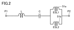
- FIG. 1 is a circuit diagram of a filter device according to Embodiment 1;
- FIG. 2 is an exploded plan view showing the configuration of the filter device according to Embodiment 1;
- FIG. FIG. 4 is an exploded plan view of the configuration of the filter device according to Embodiment 1 when stacking deviation occurs in one direction;
- FIG. 10 is an exploded plan view of the configuration of the filter device according to Embodiment 1 when stacking misalignment occurs in the other direction;
- FIG. 4 is an exploded plan view showing a configuration of a modified example of the filter device according to Embodiment 1;
- FIG. 9 is an exploded plan view showing the configuration of another modified example of the filter device according to Embodiment 1;
- FIG. 11 is a perspective view of a filter device according to Embodiment 2;
- FIG. 5 is a circuit diagram of a filter device according to Embodiment 2;
- FIG. 8 is an exploded plan view showing the configuration of a filter device according to Embodiment 2;
- FIG. 11 is an exploded plan view showing a configuration of a modified example of the filter device according to Embodiment 2;
- FIG. 9 is a cross-sectional view showing the configuration of another modified example of the filter device according to Embodiment 2;
- FIG. 9 is an exploded plan view showing the configuration of a filter device according to Modification 1;
- FIG. 11 is an exploded plan view showing the configuration of a filter device according to Modification 2;
- FIG. 11 is an exploded plan view showing the configuration of a filter device according to Modification 3;
- a filter device as an example of an electronic component according to an embodiment will be described in detail below with reference to the drawings.
- the same or corresponding parts in the drawings are denoted by the same reference numerals, and the description thereof will not be repeated.
- the electronic component according to the embodiment is not limited to a filter device.
- FIG. 1 is a perspective view of a filter device 100 according to Embodiment 1.
- the short side direction of the filter device 100 is the X direction
- the long side direction is the Y direction
- the height direction is the Z direction.
- the filter device 100 is a rectangular parallelepiped chip component in which one inductor and one capacitor are laminated in the Z direction.
- the filter device 100 is composed of an insulator 3 in which a plurality of insulating substrates (insulator layers) on which conductor patterns of inductors L and electrode patterns of capacitors C are formed are laminated as shown in FIG.
- the stacking direction of the insulating substrates is the Z direction, and the direction of the arrow indicates the upper layer direction.
- the insulating substrate is made of, for example, an insulating material containing borosilicate glass as a main component, or an insulating resin such as alumina, zirconia, or polyimide resin.
- the insulator 3 may not have a clear boundary between the insulating substrates due to baking, hardening, or the like.
- two external electrodes 4a first external electrodes
- an external electrode 4b second external electrode
- the insulator 3 has a pair of main surfaces facing each other, the lower main surface in FIG. 1 being the mounting surface, and this surface facing the circuit board.
- the main surface on the lower side of FIG. 1 is also called a bottom surface
- the main surface on the upper side of FIG. 1 is also called a top surface.
- the external electrodes 4 a and 4 b have electrode patterns formed not only on the bottom surface of the insulator 3 , but also on the side surfaces connecting the main surfaces of the insulator 3 .
- the external electrodes 4a and 4b are U-shaped. Therefore, the external electrodes 4 a provided on the opposite side surfaces of the insulator 3 are at the same potential due to the electrode pattern provided on the bottom surface of the insulator 3 .
- the external electrodes 4b provided on the opposite side surfaces of the insulator 3 are at the same potential due to the electrode pattern provided on the bottom surface of the insulator 3 .
- both the external electrode 4a and the external electrode 4b are provided with electrode patterns on the opposite side surfaces of the insulator 3 as well.
- the external electrode 4a is not provided with electrode patterns on both of the opposite side surfaces of the insulator 3.
- the external electrodes 4a may be formed not on the same surface as the external electrodes 4b but on the side surface on the short side.
- the conductor pattern 1a (first conductor pattern) of the inductor L and the external electrode 4a are electrically connected on the side surface of the insulator 3 via the wiring pattern 11a.
- the electrode pattern 5b (second electrode pattern) of the capacitor C and the external electrode 4b are electrically connected on the side surface of the insulator 3 via the wiring pattern 51a (see FIG. 3) and the wiring pattern 51b.
- the inductor L is formed by stacking a plurality of conductor patterns 1a and 1b parallel to the main surface of the insulator 3, and electrically connecting the conductor patterns 1a and 1b with via conductors 31 and 32 and the like.
- a plurality of electrode patterns 5a and 5b are stacked under the inductor L via an insulating layer.
- the capacitor C is provided at a position within the insulator 3 that partially overlaps the conductor patterns 1a and 1b when viewed from one of the main surfaces (the top surface).
- the inductor L and the capacitor C are connected in series within the insulator 3 to form an LC series circuit.
- FIG. 2 is a circuit diagram of the filter device 100 according to Embodiment 1.
- FIG. Filter device 100 includes a first terminal P1, an inductor L connected to first terminal P1, a capacitor C connected in series with inductor L, and a second terminal P2 connected to capacitor C.
- the first terminal P1 corresponds to the external electrode 4a shown in FIG. 1
- the second terminal P2 corresponds to the external electrode 4b shown in FIG.
- parasitic inductances ESL1 and ESL2 are illustrated between the capacitor C and the second terminal P2.
- Parasitic inductances ESL1 and ESL2 are generated in wiring patterns 51a and 51b for connecting electrode pattern 5b of capacitor C and external electrode 4b.
- FIG. 3 is an exploded plan view showing the configuration of the filter device 100 according to Embodiment 1.
- conductor patterns 1a and 1b, wiring patterns 11a, 51a and 51b, and electrode patterns 5a and 5b are each formed on insulating substrates 3a to 3d by a printing method.
- a conductor pattern 1a forming part of the inductor L is formed on the insulating substrate 3a.
- the conductor pattern 1a is formed so as to extend clockwise about 3/4 from the upper left side of the insulating substrate 3a in the figure.
- the starting end of the conductor pattern 1a is electrically connected to the external electrode 4a through the wiring pattern 11a.
- a connection portion 31a connected to the via conductor 31 and a connection portion 32a connected to the via conductor 32 are provided in the vicinity of the terminal end of the conductor pattern 1a.
- a conductor pattern 1b forming part of the inductor L is formed on the insulating substrate 3b.
- the conductor pattern 1b is formed so as to extend clockwise about 3/4 from the lower side of the insulating substrate 3b in the figure.
- a connection portion 31b connected to the via conductor 31 and a connection portion 32b connected to the via conductor 32 are provided in the vicinity of the starting end of the conductor pattern 1b.
- a connection portion 33b connected to the via conductor 33 is provided near the terminal end of the conductor pattern 1b.
- the inductor L connects the conductor patterns 1a and 1b in series to form a coil of about 1.5 turns.
- An electrode pattern 5a (first electrode pattern) forming one electrode of the capacitor C is formed on the insulating substrate 3c.
- the electrode pattern 5a is provided at a position within the insulator 3 that partially overlaps the conductor patterns 1a and 1b when viewed from the top side. That is, the electrode pattern 5a is provided at a position that does not overlap with the opening of the inductor L composed of the conductor patterns 1a and 1b as much as possible.
- the electrode pattern 5 a has a connecting portion 33 c that connects with the via conductor 33 .
- An electrode pattern 5b forming the other electrode of the capacitor C is formed on the insulating substrate 3d.
- the electrode pattern 5b is provided at a position inside the insulator 3 facing the electrode pattern 5a when viewed from above.
- the electrode pattern 5b is electrically connected to the external electrode 4b through wiring patterns 51a and 51b.
- each of the wiring patterns 51a and 51b is illustrated as one wiring, they may be configured by a plurality of wirings.
- the external electrodes 4b are provided on opposite sides of the insulator 3 as shown in FIG.
- the wiring patterns 51a and 51b electrically connect the respective external electrodes 4b and the electrode patterns 5b. Since each external electrode 4b has the same potential, the wiring patterns 51a and 51b are connected in parallel between the second terminal P2 (external electrode 4b) and the capacitor C (electrode pattern 5b) as shown in the circuit diagram of FIG. Connected. As a result, the parasitic inductances ESL1 and ESL2 caused by the wiring patterns 51a and 51b are parallel, so that the value of the parasitic inductance can be substantially reduced.
- a portion of the conductor pattern 1b overlapping the capacitor C has a portion parallel to one side (short side) of the insulator 3 facing the external electrode 4b.
- the portion of the conductor pattern 1b formed in the X direction on the right side of the drawing is parallel to one side (short side) of the insulator 3 facing the external electrode 4b. Therefore, since the conductor pattern 1b includes a portion that is in the same direction as the wiring patterns 51a and 51b, the wiring patterns 51a and 51b and the conductor pattern 1b are coupled to each other in the directions of strengthening and weakening each other. . Therefore, adjustment of the filter characteristic value of the filter device 100 is facilitated. Not only the conductor pattern 1b but also the conductor pattern 1a may be coupled to the wiring patterns 51a and 51b, and if the conductor pattern 1b and the wiring patterns 51a and 51b are not coupled, only the conductor pattern 1a is coupled. may
- the electrode patterns 5a and 5b are provided at positions that do not overlap with the opening of the inductor L composed of the conductor patterns 1a and 1b as much as possible, so that they do not interfere with the magnetic field generated by the inductor L, and the filter device 100 can be realized with small components. can be realized.
- the wiring patterns 51a and 51b are drawn out from two directions of the electrode patterns 5b as shown in FIG. Therefore, even if the wiring patterns 51a and 51b are displaced in the short side direction of the insulator 3 and the insulating substrates are stacked (stacking misalignment), the variation of the parasitic inductance can be suppressed. Therefore, it is possible to suppress variations in the characteristics of the filter device.
- FIG. 4 is an exploded plan view of the configuration of the filter device 100 according to Embodiment 1 when stacking misalignment occurs in one direction.
- FIG. 5 is an exploded plan view of the configuration of the filter device 100 according to Embodiment 1 when stacking misalignment occurs in the other direction. 4 and 5 are the same as the exploded plan view shown in FIG. 3 except that the position of the electrode pattern 5b formed on the insulating substrate 3d is shifted. Don't repeat the description.
- the position of the electrode pattern 5b formed on the insulating substrate 3d is shifted in the positive direction of the X direction (direction of the arrow). Therefore, the distance between the external electrode 4b on the upper side in the figure and the electrode pattern 5b is shortened, and the length of the wiring pattern 51a is shortened. Conversely, the distance between the lower external electrode 4b in the figure and the electrode pattern 5b increases, and the length of the wiring pattern 51b increases.
- the position of the electrode pattern 5b formed on the insulating substrate 3d is shifted in the negative direction of the X direction (the direction opposite to the arrow). Therefore, the distance between the lower external electrode 4b in the figure and the electrode pattern 5b is shortened, and the length of the wiring pattern 51b is shortened. Conversely, the distance between the external electrode 4b on the upper side in the figure and the electrode pattern 5b increases, and the length of the wiring pattern 51a increases.
- the parasitic inductance ESL1 occurring in the wiring pattern 51a is 0.10 nH
- the parasitic inductance ESL2 occurring in the wiring pattern 51b is 0.15 nH
- the total of the parasitic inductances ESL1 and ESL2 connected in parallel is 0.06 nH.
- the filter device 100 shown in FIG. The sum of ESL1 and ESL2 is 0.04 nH.
- the filter device 100 shown in FIG. 5 has a parasitic inductance ESL1 of 0.15 nH, a parasitic inductance ESL2 of 0.10 nH, and a total of the parasitic inductances ESL1 and ESL2 connected in parallel of 0.06 nH. That is, in the filter device 100, when the parasitic inductance increases or decreases due to stacking misalignment of ⁇ 0.05 nH, the total of the parasitic inductances ESL1 and ESL2 connected in parallel fluctuates between 0.04 nH and 0.06 nH.
- the filter device 100 can reduce fluctuations in parasitic inductance due to processing variations in stacking misalignment.
- FIG. 6 is an exploded plan view showing a configuration of a modification of the filter device according to Embodiment 1.
- FIG. The filter device 100A shown in FIG. 6 has a configuration in which the external electrode 4b and the electrode pattern 5b are electrically connected only by the wiring pattern 51b without providing the wiring pattern 51a. 6 is the same as the exploded plan view shown in FIG. 3 except that the wiring pattern 51a of the insulating substrate 3d is not provided. .
- a current I2 flows through the wiring pattern 51b of the insulating substrate 3d in a direction substantially parallel to and in the same direction as the current I1 flowing toward the connection portion 33b in the conductor pattern 1b of the insulating substrate 3b. Therefore, since the filter device 100A shown in FIG. 6 has the wiring pattern 51b through which the current flows in the same direction as the conductor pattern 1b, the self-induction of the inductor L is not hindered and the total reactance can be increased.
- FIG. 7 is an exploded plan view showing the configuration of another modified example of the filter device according to Embodiment 1.
- FIG. The filter device 100B shown in FIG. 7 has a configuration in which the external electrode 4b and the electrode pattern 5b are electrically connected only by the wiring pattern 51a without providing the wiring pattern 51b. 7 is the same as the exploded plan view shown in FIG. 3 except that the wiring pattern 51b of the insulating substrate 3d is not provided. .
- a current I3 flows through the wiring pattern 51a of the insulating substrate 3d in a direction substantially parallel to and opposite to the direction of the current I1 flowing toward the connection portion 33b in the conductor pattern 1b of the insulating substrate 3b. Therefore, since the filter device 100B shown in FIG. 7 has the wiring pattern 51a through which the current flows in the opposite direction to the conductor pattern 1b, the self-induction of the inductor L can be prevented and the total reactance can be reduced.
- the inductance value of the inductor L can also be adjusted by using one of the pattern 51a and the wiring pattern 51b.
- the filter device 100 includes the insulator 3, the inductor L, the capacitor C, the external electrodes 4a, and the external electrodes 4b.
- the insulator 3 has a pair of main surfaces facing each other and side surfaces connecting the main surfaces.
- the inductor L is composed of at least one conductor pattern 1a, 1b within the insulator 3.
- the capacitor C is provided at a position within the insulator 3 that partially overlaps the conductor patterns 1a and 1b when viewed from one of the main surfaces.
- the external electrode 4a is electrically connected to the inductor L.
- the external electrodes 4 b are electrically connected to the capacitors C and provided on opposite side surfaces of the insulator 3 .
- the capacitor C includes an electrode pattern 5a electrically connected to the inductor L, and an electrode pattern 5b electrically connected to each external electrode 4b by at least one wiring pattern 51a, 51b. At least one wiring pattern 51a, 51b is parallel to a portion of the conductor patterns 1a, 1b.
- the electrode pattern 5b of the capacitor C is electrically connected to each of the external electrodes 4b by at least one wiring pattern 51a, 51b. The influence of parasitic inductance can be reduced.
- the filter device 100 by limiting the overlapping portions of the inductor L and the capacitor C to a part of the conductor patterns 1a and 1b, it is possible to suppress the reduction in the Q value due to the generation of eddy currents in the electrode patterns 5a and 5b. can do.
- the electrode pattern 5b of the capacitor C and each of the external electrodes 4b are electrically connected by two wiring patterns 51a and 51b arranged linearly.
- portions of the conductor patterns 1a and 1b overlapping the capacitor C are parallel to one side of the insulator 3 facing the external electrode 4b. is preferred.
- the wiring patterns 51a and 51b partially overlap the conductor patterns 1a and 1b when viewed from one of the main surfaces (the top surface). This facilitates adjustment of the filter design of the filter device 100 .
- Each external electrode 4b has the same potential.
- the wiring patterns 51a and 51b having the parasitic inductances ESL1 and ESL2 are connected in parallel.
- the inductor L and capacitor C form an LC series circuit. This results in the filter device 100 having an LC series circuit. Since a filter using an LC series circuit uses the series resonance frequency as a pass band, the resonance frequency is shifted due to parasitic inductance, which may lead to deterioration in performance as a pass filter. Therefore, it is particularly important in the LC series circuit to suppress variations in the parasitic inductance due to the wiring pattern of the capacitor C. FIG.
- filter device 100 is described as a rectangular parallelepiped chip component in which inductor L and capacitor C are stacked in the Z direction.
- filter device 100 is described as a rectangular parallelepiped chip component in which inductor L and capacitor C are stacked in the Z direction.
- a filter device to which an inductor is further added will be described.
- FIG. 8 is a perspective view of a filter device 200 according to Embodiment 2.
- the short side direction of the filter device 200 is the X direction
- the long side direction is the Y direction
- the height direction is the Z direction.
- filter device 200 shown in FIG. 8 the same components as those of filter device 100 shown in FIG. 1 are denoted by the same reference numerals, and detailed description thereof will not be repeated.
- the filter device 200 is a rectangular parallelepiped chip component in which two inductors and one capacitor are stacked in the Z direction.
- the filter device 200 has a pair of main surfaces facing each other, the lower main surface in FIG. 8 being the mounting surface, and this surface facing the circuit board.
- the main surface on the lower side of FIG. 8 is also called a bottom surface
- the main surface on the upper side of FIG. 8 is also called a top surface.
- Filter device 200 includes a plurality of insulating substrates (insulator layers) on which a first conductor pattern of first inductor L1, a second conductor pattern of second inductor L2, and an electrode pattern of capacitor C are formed, as shown in FIG. It is composed of laminated insulators 3 .
- the stacking direction of the insulating substrates is the Z direction, and the direction of the arrow indicates the upper layer direction.
- the filter device 200 has a capacitor C, a first inductor L1, and a second inductor L2 stacked in this order in the Z direction.
- an external electrode 4a (first external electrode) and an external electrode 4b (second external electrode) are formed on the insulator 3 at two locations in the Y direction, as shown in FIG.
- the first conductor patterns 1E, 1F of the first inductor L1 and the external electrode 4a are electrically connected on the side surface of the insulator 3 via the wiring patterns 11E, 11F.
- the second conductor patterns 2A, 2B of the second inductor L2 and the external electrode 4b are electrically connected on the side surface of the insulator 3 via the wiring patterns 12A, 12B.
- the second conductor patterns 2C, 2D of the second inductor L2 and the external electrode 4a are electrically connected on the side surface of the insulator 3 via the wiring patterns 12C, 12D.
- the electrode pattern 5b (second electrode pattern) of the capacitor C and the external electrode 4b are electrically connected on the side surface of the insulator 3 via the wiring pattern 51a (see FIG. 10) and the wiring pattern 51b.
- first inductor L1 a plurality of first conductor patterns 1E to 1H are stacked parallel to the main surface of the insulator 3, and each of the first conductor patterns 1E to 1H is electrically connected by via conductors 31, 32 and the like. It is connected.
- the second inductor L2 is formed by stacking a plurality of second conductor patterns 2A to 2D parallel to the main surface of the insulator 3 and electrically connecting the respective second conductor patterns 2A to 2D with via conductors 34.
- the capacitor C has a plurality of electrode patterns 5a and 5b stacked under the first inductor L1 via an insulating layer.
- the capacitor C is provided at a position within the insulator 3 overlapping with a part of the first conductor patterns 1G and 1H when viewed from one of the principal surfaces (top surface).
- Filter device 200 forms a circuit in which first inductor L1 and capacitor C are connected in series within insulator 3, and second inductor L2 is connected in parallel to first inductor L1 and capacitor C. .
- FIG. 9 is a circuit diagram of the filter device 200 according to the second embodiment.
- the filter device 200 includes a first terminal P1, a first inductor L1 connected to the first terminal P1, a capacitor C connected in series with the first inductor L1, and a second terminal P2 connected to the capacitor C. ,including. Further, filter device 200 includes a second inductor L2 connected in parallel with first inductor L1 and capacitor C connected in series.
- the first inductor L1 and the second inductor L2 are magnetically coupled (coupling coefficient k) with each other. Thereby, a mutual inductance M is generated between the first inductor L1 and the second inductor L2.
- the filter device 200 is not limited to the case where the first inductor L1 and the second inductor L2 are magnetically coupled to each other. may
- the first terminal P1 corresponds to the external electrode 4a shown in FIG. 8, and the second terminal P2 corresponds to the external electrode 4b shown in FIG.
- the circuit diagram of the filter device 200 shown in FIG. 9 shows parasitic inductances ESL1 and ESL2 between the capacitor C and the second terminal P2.
- Parasitic inductances ESL1 and ESL2 are generated in wiring patterns 51a and 51b for connecting electrode pattern 5b of capacitor C and external electrode 4b.
- FIG. 10 is an exploded plan view showing the configuration of filter device 200 according to the second embodiment.
- each of the first conductor patterns 1E to 1H, the second conductor patterns 2A to 2D, the wiring patterns 12A to 12D, 11E, 11F, 51a and 51b, and the electrode patterns 5a and 5b are insulated. It is formed on the substrates 3A to 3J by a printing method.
- a second conductor pattern 2A forming part of the second inductor L2 is formed on the insulating substrate 3A.
- the second conductor pattern 2A is formed so as to make about one turn clockwise from the upper right side of the insulating substrate 3A in the figure.
- the starting end of the second conductor pattern 2A is electrically connected to the external electrode 4b via the wiring pattern 12A.
- a connection portion 34A connected to the via conductor 34 is provided at the end of the second conductor pattern 2A.
- a second conductor pattern 2B forming part of the second inductor L2 is formed on the insulating substrate 3B.
- the second conductor pattern 2B is formed so as to make about one turn clockwise from the upper right side of the insulating substrate 3B in the figure.
- the starting end of the second conductor pattern 2B is electrically connected to the external electrode 4b via the wiring pattern 12B.
- a connection portion 34B connected to the via conductor 34 is provided at the end of the second conductor pattern 2B.
- a second conductor pattern 2C forming part of the second inductor L2 is formed on the insulating substrate 3C.
- the second conductor pattern 2C is formed so as to make about one turn clockwise from the upper side of the insulating substrate 3C in the figure.
- a connection portion 34C that connects to the via conductor 34 is provided at the beginning of the second conductor pattern 2C.
- the end of the second conductor pattern 2C is electrically connected to the external electrode 4a through the wiring pattern 12C.
- a second conductor pattern 2D forming part of the second inductor L2 is formed on the insulating substrate 3D.
- the second conductor pattern 2D is formed so as to make about one turn clockwise from the upper side of the insulating substrate 3D in the drawing.
- a connection portion 34D connected to the via conductor 34 is provided at the beginning of the second conductor pattern 2D.
- the end of the second conductor pattern 2D is electrically connected to the external electrode 4a through the wiring pattern 12D.
- the second inductor L2 has second conductor patterns 2A and 2B and second conductor patterns 2C and 2D connected in parallel, respectively, and the second conductor patterns 2A and 2B connected in parallel and the second conductor patterns 2C and 2C connected in parallel. 2D are connected in series to form a coil of about two turns.
- a first conductor pattern 1E forming part of the first inductor L1 is formed on the insulating substrate 3E.
- the first conductor pattern 1E is formed so as to extend clockwise about 3/4 from the upper left side of the insulating substrate 3E in the figure.
- the starting end of the first conductor pattern 1E is electrically connected to the external electrode 4a through the wiring pattern 11E.
- a connection portion 31E connected to the via conductor 31 and a connection portion 32E connected to the via conductor 32 are provided near the end of the first conductor pattern 1E.
- a first conductor pattern 1F forming part of the first inductor L1 is formed on the insulating substrate 3F.
- the first conductor pattern 1F is formed so as to extend clockwise about 3/4 from the upper left side of the insulating substrate 3F in the drawing.
- the starting end of the first conductor pattern 1F is electrically connected to the external electrode 4a via the wiring pattern 11F.
- a connection portion 31F connected to the via conductor 31 and a connection portion 32F connected to the via conductor 32 are provided near the end of the first conductor pattern 1F.
- a first conductor pattern 1G forming a part of the first inductor L1 is formed on the insulating substrate 3G.
- the first conductor pattern 1G is formed so as to extend clockwise about 3/4 from the lower side of the insulating substrate 3G in the figure.
- a connection portion 31G connected to the via conductor 31 and a connection portion 32G connected to the via conductor 32 are provided in the vicinity of the starting end of the first conductor pattern 1G.
- a connection portion 33G connected to the via conductor 33 is provided near the end of the first conductor pattern 1G.
- a first conductor pattern 1H forming part of the first inductor L1 is formed on the insulating substrate 3H.
- the first conductor pattern 1H is formed so as to extend clockwise about 3/4 from the lower side of the insulating substrate 3H in the figure.
- a connection portion 31H connected to the via conductor 31 and a connection portion 32H connected to the via conductor 32 are provided in the vicinity of the starting end of the first conductor pattern 1H.
- a connection portion 33H connected to the via conductor 33 is provided near the end of the first conductor pattern 1H.
- the first conductor patterns 1E, 1F and the first conductor patterns 1G, 1H are connected in parallel, respectively, and the first conductor patterns 1G, 1F are connected in parallel with the first conductor patterns 1E, 1F connected in parallel. 1H are connected in series to form a coil of about 1.5 turns.
- An electrode pattern 5a (first electrode pattern) forming one electrode of the capacitor C is formed on the insulating substrate 3I.
- the electrode pattern 5a is provided at a position within the insulator 3 that partially overlaps the first conductor patterns 1G and 1H when viewed from the top surface side. That is, the electrode pattern 5a is provided at a position that does not overlap with the opening of the first inductor L1 composed of the first conductor patterns 1G and 1H as much as possible.
- the electrode pattern 5 a has a connecting portion 33 ⁇ /b>I that connects with the via conductor 33 .
- An electrode pattern 5b forming the other electrode of the capacitor C is formed on the insulating substrate 3J.
- the electrode pattern 5b is provided at a position inside the insulator 3 facing the electrode pattern 5a when viewed from above.
- the electrode pattern 5b is electrically connected to the external electrode 4b through wiring patterns 51a and 51b.
- each of the wiring patterns 51a and 51b is illustrated as one wiring, they may be configured by a plurality of wirings.
- the external electrodes 4b are provided on opposite side surfaces of the insulator 3, as shown in FIG.
- the wiring patterns 51a and 51b electrically connect the respective external electrodes 4b and the electrode patterns 5b.
- the external electrodes 4b have the same potential. That is, the wiring patterns 51a and 51b are connected in parallel between the second terminal P2 (external electrode 4b) and the capacitor C (electrode pattern 5b) as shown in the circuit diagram of FIG.
- the parasitic inductances ESL1 and ESL2 caused by the wiring patterns 51a and 51b are parallel, so that the value of the parasitic inductance can be substantially reduced.
- filter device 200 has the same effects as filter device 100 described in the first embodiment.
- the external electrodes 4a, 4b shown in FIG. ) are not provided with electrodes.
- the shape of the external electrode is not limited to this, and it may be a dogbone-shaped external electrode in which electrodes are also provided on the short side surface (XZ plane) of the insulator 3 .
- FIG. 11 is an exploded plan view showing the configuration of a modified example of the filter device according to Embodiment 2.
- FIG. 11 In the filter device 200A shown in FIG. 11, dogbone-shaped external electrodes 4c and 4d are used, and wiring for connecting the external electrodes 4c and 4d to the first conductor patterns 1E and 1F and the second conductor patterns 2A to 2D. The patterns are changed to 22A to 22D, 21E and 21F.
- 11 is the same as the exploded plan view shown in FIG. 10 except that the external electrodes 4c and 4d and the wiring patterns 22A to 22D, 21E and 21F are changed. and do not repeat the detailed description.
- the second conductor pattern 2A of the insulating substrate 3A is electrically connected to the external electrode 4d through the wiring pattern 22A on the short side of the insulating substrate 3A on the right side in the figure.
- the second conductor pattern 2B of the insulating substrate 3B is electrically connected to the external electrode 4d through the wiring pattern 22B on the short side of the insulating substrate 3B on the right side in the figure.
- the second conductor pattern 2C of the insulating substrate 3C is electrically connected to the external electrode 4c via the wiring pattern 22C on the short side of the insulating substrate 3C on the left side in the drawing.
- the second conductor pattern 2D of the insulating substrate 3D is electrically connected to the external electrode 4c through the wiring pattern 22D on the short side of the insulating substrate 3D on the left side in the figure.
- the first conductor pattern 1E of the insulating substrate 3E is electrically connected to the external electrode 4c through the wiring pattern 21E on the short side of the insulating substrate 3E on the left side in the figure.
- the first conductor pattern 1F of the insulating substrate 3F is electrically connected to the external electrode 4c through the wiring pattern 21F on the short side of the insulating substrate 3F on the left side in the figure.
- the first conductor pattern 1G of the insulating substrate 3G is electrically connected to the first conductor patterns 1E, 1F through via conductors 31, 32.
- first conductor pattern 1H of insulating substrate 3H is electrically connected to first conductor patterns 1E, 1F, and 1G through via conductors 31 and 32, respectively.
- the electrode pattern 5a (first electrode pattern) of the insulating substrate 3I constitutes one electrode of the capacitor C and has a connecting portion 33I that connects with the via conductor 33 .
- the electrode pattern 5b (second electrode pattern) of the insulating substrate 3J constitutes the other electrode of the capacitor C, and is connected to the external electrode 4d through wiring patterns 51a and 51b in parallel with a part of the first conductor patterns 1G and 1H. Of these, the opposing sides are electrically connected. Further, it may have a wiring pattern 51c connected to the external electrode 4d in a direction different from that of the wiring patterns 51a and 51b.
- the dogbone-shaped external electrodes 4c and 4d described for the filter device 200A can be similarly applied to the filter devices 100, 100A and 100B according to the first embodiment.
- the filter device 200 further includes the second inductor L2 configured by at least one second conductor pattern within the insulator 3.
- the second inductor L2 configured by at least one second conductor pattern within the insulator 3.
- the second inductor L2 is preferably connected in parallel with the first inductor L1. Moreover, it is preferable that the second inductor L2 is magnetically coupled to the first inductor L1. In the filter device 200A, an example in which two layers of each conductor pattern are connected in parallel has been shown.
- FIG. 10 it functions as a bandpass filter that passes Wi-Fi (registered trademark) 5 GHz band signals and blocks 5th generation n78 (3.7 GHz band) and n79 (4.5 GHz band) signals.
- the filter device 200 has been described. In the modification below, a filter device that functions as a bandpass filter that passes signals in the 2.4 GHz band of Wi-Fi (registered trademark) and blocks signals in the GPS band (1.1 to 1.6 GHz) will be described. do.
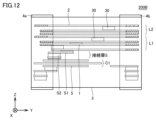
- FIG. 12 is a cross-sectional view showing the configuration of another modified example of the filter device according to Embodiment 2.
- FIG. In the filter device 200B shown in FIG. 12 the capacitor C1, the first inductor L1, and the second inductor L2 are stacked in this order in the Z direction, and the first inductor L1 and the second inductor L2 are magnetically coupled.
- the second inductor L2 is formed by stacking three layers of second conductor patterns 2 parallel to the main surface of the insulator 3, and electrically connecting the respective second conductor patterns 2 with via conductors 30. ing.
- the first inductor L1 four layers of first conductor patterns 1 are stacked parallel to the main surface of the insulator 3, and the respective first conductor patterns 1 are electrically connected by via conductors 30.
- the capacitor C1 has a plurality of electrode patterns 5 stacked under the first inductor L1 via an insulating layer.
- the capacitor C1 becomes large. As the capacitor C1 increases, the area of the electrode pattern 5 increases, and when viewed from above, the electrode pattern 5 overlaps the openings of the first inductor L1 and the second inductor L2 by more than half. Therefore, in the filter device 200B, the connection layer S is provided between the first inductor L1 and the capacitor C1 to secure the distance in the stacking direction between the first inductor L1 and the capacitor C1. For example, the distance in the stacking direction between the first inductor L1 and the capacitor C1 is made longer than the distance in the stacking direction between the first inductor L1 and the second inductor L2.
- connection layer S is composed of a plurality of conductive patterns S1 and via conductors S2.
- the conductive patterns of the inductor L, the first inductor L1, and the second inductor L2 described so far have a rectangular shape.
- a rectangular conductor pattern is adopted because a conductor pattern can be formed all over the outer frame of the insulator 3 to ensure a high inductance value.
- the shape of the conductive pattern is not limited to a rectangular shape, and may be a polygonal shape such as an octagon, or a curved shape such as an ellipse.
- FIG. 13 is an exploded plan view showing the configuration of a filter device 100C according to Modification 1.
- the filter device 100C is a rectangular parallelepiped chip component in which one inductor and one capacitor are laminated in the Z direction.
- the filter device 100C is composed of an insulator 3 in which a plurality of insulating substrates 3a to 3d on which conductor patterns of inductors L and electrode patterns of capacitors C are formed are laminated, as shown in FIG. 13, the same components as those in the exploded plan view shown in FIG. 3 are denoted by the same reference numerals, and detailed description thereof will not be repeated.
- a conductor pattern 1a forming part of the inductor L is formed on the insulating substrate 3a.
- the conductor pattern 1a is not rectangular but octagonal.
- a portion of the conductor pattern 1a overlapping the capacitor C has a portion parallel to one side (short side) of the insulator 3 facing the external electrode 4b. Therefore, as shown in FIG. 13, the direction Da of a portion of the conductor pattern 1a and the wiring direction Dd of the wiring patterns 51a and 51b of the insulating substrate 3d are substantially parallel.
- a conductor pattern 1b forming part of the inductor L is formed on the insulating substrate 3b.
- the conductor pattern 1b is not rectangular but octagonal.
- a portion of the conductor pattern 1b overlapping the capacitor C has a portion parallel to one side (short side) of the insulator 3 facing the external electrode 4b. Therefore, as shown in FIG. 13, the direction Db of a portion of the conductor pattern 1b and the wiring direction Dd of the wiring patterns 51a and 51b of the insulating substrate 3d are substantially parallel.
- FIG. 14 is an exploded plan view showing the configuration of a filter device 100D according to Modification 2.
- the filter device 100D is a rectangular parallelepiped chip component in which one inductor and one capacitor are laminated in the Z direction.
- the filter device 100D is composed of an insulator 3 in which a plurality of insulating substrates 3a to 3d on which conductor patterns of inductors L and electrode patterns of capacitors C are formed are laminated as shown in FIG. 14, the same components as those in the exploded plan view shown in FIG. 3 are denoted by the same reference numerals, and detailed description thereof will not be repeated.
- a conductor pattern 1a forming part of the inductor L is formed on the insulating substrate 3a.
- the conductor pattern 1a is not rectangular but hexagonal.
- a portion of the conductor pattern 1a overlapping the capacitor C has a portion parallel to one side (short side) of the insulator 3 facing the external electrode 4b. Therefore, as shown in FIG. 14, the direction Da of a portion of the conductor pattern 1a and the wiring direction Dd of the wiring patterns 51a and 51b of the insulating substrate 3d are substantially parallel.
- a conductor pattern 1b forming part of the inductor L is formed on the insulating substrate 3b.
- the conductor pattern 1b is hexagonal rather than rectangular.
- a portion of the conductor pattern 1b overlapping the capacitor C has a portion parallel to one side (short side) of the insulator 3 facing the external electrode 4b. Therefore, as shown in FIG. 14, the direction Db of a portion of the conductor pattern 1b and the wiring direction Dd of the wiring patterns 51a and 51b of the insulating substrate 3d are substantially parallel.
- FIG. 15 is an exploded plan view showing the configuration of a filter device 100E according to Modification 3.
- the filter device 100E is a rectangular parallelepiped chip component in which one inductor and one capacitor are laminated in the Z direction.
- the filter device 100E is composed of an insulator 3 in which a plurality of insulating substrates 3a to 3d on which conductor patterns of inductors L and electrode patterns of capacitors C are formed are laminated as shown in FIG. 15, the same components as those in the exploded plan view shown in FIG. 3 are denoted by the same reference numerals, and detailed description thereof will not be repeated.
- a conductor pattern 1a forming part of the inductor L is formed on the insulating substrate 3a.
- the conductor pattern 1a is elliptical rather than rectangular.
- a portion of the conductor pattern 1a overlapping the capacitor C has a portion parallel to one side (short side) of the insulator 3 facing the external electrode 4b. Therefore, as shown in FIG. 15, the direction Da of a portion of the conductor pattern 1a and the wiring direction Dd of the wiring patterns 51a and 51b of the insulating substrate 3d are substantially parallel.
- a conductor pattern 1b forming part of the inductor L is formed on the insulating substrate 3b.
- the conductor pattern 1b is elliptical rather than rectangular.
- a portion of the conductor pattern 1b overlapping the capacitor C has a portion parallel to one side (short side) of the insulator 3 facing the external electrode 4b. Therefore, as shown in FIG. 15, the direction Db of a portion of the conductor pattern 1b and the wiring direction Dd of the wiring patterns 51a and 51b of the insulating substrate 3d are substantially parallel.
- 3 insulator 4a to 4d external electrodes, 10 circuit board, 100, 100A to E, 200, 200A filter device, C capacitor, L1 first coil, L2 second coil.
Landscapes
- Engineering & Computer Science (AREA)
- Power Engineering (AREA)
- Microelectronics & Electronic Packaging (AREA)
- Manufacturing & Machinery (AREA)
- Filters And Equalizers (AREA)
- Coils Or Transformers For Communication (AREA)
Priority Applications (3)
| Application Number | Priority Date | Filing Date | Title |
|---|---|---|---|
| CN202380015523.0A CN118648075A (zh) | 2022-02-04 | 2023-01-24 | 电子部件 |
| JP2023578491A JP7750313B2 (ja) | 2022-02-04 | 2023-01-24 | 電子部品 |
| US18/740,570 US20240331935A1 (en) | 2022-02-04 | 2024-06-12 | Electronic component |
Applications Claiming Priority (2)
| Application Number | Priority Date | Filing Date | Title |
|---|---|---|---|
| JP2022-016416 | 2022-02-04 | ||
| JP2022016416 | 2022-02-04 |
Related Child Applications (1)
| Application Number | Title | Priority Date | Filing Date |
|---|---|---|---|
| US18/740,570 Continuation US20240331935A1 (en) | 2022-02-04 | 2024-06-12 | Electronic component |
Publications (1)
| Publication Number | Publication Date |
|---|---|
| WO2023149279A1 true WO2023149279A1 (ja) | 2023-08-10 |
Family
ID=87552243
Family Applications (1)
| Application Number | Title | Priority Date | Filing Date |
|---|---|---|---|
| PCT/JP2023/002074 Ceased WO2023149279A1 (ja) | 2022-02-04 | 2023-01-24 | 電子部品 |
Country Status (4)
| Country | Link |
|---|---|
| US (1) | US20240331935A1 (https=) |
| JP (1) | JP7750313B2 (https=) |
| CN (1) | CN118648075A (https=) |
| WO (1) | WO2023149279A1 (https=) |
Citations (4)
| Publication number | Priority date | Publication date | Assignee | Title |
|---|---|---|---|---|
| JPH0339824U (https=) * | 1989-08-29 | 1991-04-17 | ||
| JPH05308023A (ja) * | 1992-05-01 | 1993-11-19 | Murata Mfg Co Ltd | 複合電子部品 |
| JP2011124880A (ja) * | 2009-12-11 | 2011-06-23 | Murata Mfg Co Ltd | 積層バランスフィルタ |
| WO2019003723A1 (ja) * | 2017-06-30 | 2019-01-03 | 株式会社村田製作所 | 積層バラン |
Family Cites Families (10)
| Publication number | Priority date | Publication date | Assignee | Title |
|---|---|---|---|---|
| CN105684305B (zh) * | 2013-10-30 | 2018-04-24 | 株式会社村田制作所 | 电子元器件 |
| JP5970714B2 (ja) * | 2013-10-30 | 2016-08-17 | 株式会社村田製作所 | 電子部品 |
| JP6288386B2 (ja) * | 2015-10-02 | 2018-03-07 | 株式会社村田製作所 | 表面実装型lcデバイス |
| KR101883046B1 (ko) * | 2016-04-15 | 2018-08-24 | 삼성전기주식회사 | 코일 전자 부품 |
| JP6743767B2 (ja) * | 2017-06-06 | 2020-08-19 | 株式会社村田製作所 | Lc複合部品 |
| JP7609177B2 (ja) * | 2021-02-05 | 2025-01-07 | 株式会社村田製作所 | 電子部品、電子部品の製造方法、フィルタモジュール及び電子機器 |
| WO2023080009A1 (ja) * | 2021-11-02 | 2023-05-11 | 株式会社村田製作所 | フィルタ装置、アンテナ装置、およびアンテナモジュール |
| JP2023144819A (ja) * | 2022-03-28 | 2023-10-11 | Tdk株式会社 | 電子部品 |
| JP7677238B2 (ja) * | 2022-06-02 | 2025-05-15 | 株式会社村田製作所 | 受動部品、三次元デバイスおよび受動部品の製造方法 |
| JP2024175499A (ja) * | 2023-06-06 | 2024-12-18 | 株式会社村田製作所 | インダクタ部品 |
-
2023
- 2023-01-24 WO PCT/JP2023/002074 patent/WO2023149279A1/ja not_active Ceased
- 2023-01-24 CN CN202380015523.0A patent/CN118648075A/zh active Pending
- 2023-01-24 JP JP2023578491A patent/JP7750313B2/ja active Active
-
2024
- 2024-06-12 US US18/740,570 patent/US20240331935A1/en active Pending
Patent Citations (4)
| Publication number | Priority date | Publication date | Assignee | Title |
|---|---|---|---|---|
| JPH0339824U (https=) * | 1989-08-29 | 1991-04-17 | ||
| JPH05308023A (ja) * | 1992-05-01 | 1993-11-19 | Murata Mfg Co Ltd | 複合電子部品 |
| JP2011124880A (ja) * | 2009-12-11 | 2011-06-23 | Murata Mfg Co Ltd | 積層バランスフィルタ |
| WO2019003723A1 (ja) * | 2017-06-30 | 2019-01-03 | 株式会社村田製作所 | 積層バラン |
Also Published As
| Publication number | Publication date |
|---|---|
| US20240331935A1 (en) | 2024-10-03 |
| CN118648075A (zh) | 2024-09-13 |
| JP7750313B2 (ja) | 2025-10-07 |
| JPWO2023149279A1 (https=) | 2023-08-10 |
Similar Documents
| Publication | Publication Date | Title |
|---|---|---|
| JP7322934B2 (ja) | コイル部品および、これを含むフィルタ回路 | |
| US8680950B2 (en) | Multilayer bandpass filter | |
| JP6801826B2 (ja) | フィルタ素子 | |
| US10497510B2 (en) | Electronic component | |
| US10748698B2 (en) | Electronic component | |
| KR20190053171A (ko) | 공통 모드 노이즈 필터 | |
| US7439842B2 (en) | Laminated balun transformer | |
| US20240339982A1 (en) | Filter device, high-frequency module, and communication device | |
| WO2023149279A1 (ja) | 電子部品 | |
| US20240347257A1 (en) | Electronic component | |
| US10950381B2 (en) | Surface-mounted LC device | |
| US20230318560A1 (en) | Band-pass filter | |
| US12288119B2 (en) | Coil component | |
| US20250357908A1 (en) | Electronic component | |
| US20240331922A1 (en) | Electronic component | |
| TWI833683B (zh) | 電路板模組 | |
| WO2023157666A1 (ja) | インダクタ、およびインダクタを備えた電子部品 | |
| US20260128493A1 (en) | Electronic component | |
| JP4818303B2 (ja) | 積層チップ型高周波半導体装置 | |
| US20250309852A1 (en) | Filter device | |
| US20230307171A1 (en) | Electronic component | |
| CN118414680A (zh) | 电子部件 | |
| WO2023149240A1 (ja) | 電子部品 | |
| WO2024224724A1 (ja) | フィルタ装置、およびアンテナ装置 | |
| WO2025203829A1 (ja) | 電子部品 |
Legal Events
| Date | Code | Title | Description |
|---|---|---|---|
| 121 | Ep: the epo has been informed by wipo that ep was designated in this application |
Ref document number: 23749595 Country of ref document: EP Kind code of ref document: A1 |
|
| ENP | Entry into the national phase |
Ref document number: 2023578491 Country of ref document: JP Kind code of ref document: A |
|
| WWE | Wipo information: entry into national phase |
Ref document number: 202380015523.0 Country of ref document: CN |
|
| NENP | Non-entry into the national phase |
Ref country code: DE |
|
| 122 | Ep: pct application non-entry in european phase |
Ref document number: 23749595 Country of ref document: EP Kind code of ref document: A1 |