WO2023149131A1 - 半導体装置および半導体装置の製造方法 - Google Patents
半導体装置および半導体装置の製造方法 Download PDFInfo
- Publication number
- WO2023149131A1 WO2023149131A1 PCT/JP2022/047790 JP2022047790W WO2023149131A1 WO 2023149131 A1 WO2023149131 A1 WO 2023149131A1 JP 2022047790 W JP2022047790 W JP 2022047790W WO 2023149131 A1 WO2023149131 A1 WO 2023149131A1
- Authority
- WO
- WIPO (PCT)
- Prior art keywords
- type
- region
- impurity concentration
- semiconductor region
- semiconductor
- Prior art date
- Legal status (The legal status is an assumption and is not a legal conclusion. Google has not performed a legal analysis and makes no representation as to the accuracy of the status listed.)
- Ceased
Links
Images



Classifications
-
- H—ELECTRICITY
- H10—SEMICONDUCTOR DEVICES; ELECTRIC SOLID-STATE DEVICES NOT OTHERWISE PROVIDED FOR
- H10P—GENERIC PROCESSES OR APPARATUS FOR THE MANUFACTURE OR TREATMENT OF DEVICES COVERED BY CLASS H10
- H10P14/00—Formation of materials, e.g. in the shape of layers or pillars
- H10P14/20—Formation of materials, e.g. in the shape of layers or pillars of semiconductor materials
- H10P14/29—Formation of materials, e.g. in the shape of layers or pillars of semiconductor materials characterised by the substrates
- H10P14/2901—Materials
- H10P14/2902—Materials being Group IVA materials
- H10P14/2904—Silicon carbide
-
- H—ELECTRICITY
- H10—SEMICONDUCTOR DEVICES; ELECTRIC SOLID-STATE DEVICES NOT OTHERWISE PROVIDED FOR
- H10D—INORGANIC ELECTRIC SEMICONDUCTOR DEVICES
- H10D12/00—Bipolar devices controlled by the field effect, e.g. insulated-gate bipolar transistors [IGBT]
- H10D12/01—Manufacture or treatment
- H10D12/031—Manufacture or treatment of IGBTs
-
- H—ELECTRICITY
- H10—SEMICONDUCTOR DEVICES; ELECTRIC SOLID-STATE DEVICES NOT OTHERWISE PROVIDED FOR
- H10D—INORGANIC ELECTRIC SEMICONDUCTOR DEVICES
- H10D30/00—Field-effect transistors [FET]
- H10D30/01—Manufacture or treatment
- H10D30/021—Manufacture or treatment of FETs having insulated gates [IGFET]
-
- H—ELECTRICITY
- H10—SEMICONDUCTOR DEVICES; ELECTRIC SOLID-STATE DEVICES NOT OTHERWISE PROVIDED FOR
- H10D—INORGANIC ELECTRIC SEMICONDUCTOR DEVICES
- H10D30/00—Field-effect transistors [FET]
- H10D30/60—Insulated-gate field-effect transistors [IGFET]
-
- H—ELECTRICITY
- H10—SEMICONDUCTOR DEVICES; ELECTRIC SOLID-STATE DEVICES NOT OTHERWISE PROVIDED FOR
- H10D—INORGANIC ELECTRIC SEMICONDUCTOR DEVICES
- H10D62/00—Semiconductor bodies, or regions thereof, of devices having potential barriers
- H10D62/10—Shapes, relative sizes or dispositions of the regions of the semiconductor bodies; Shapes of the semiconductor bodies
-
- H—ELECTRICITY
- H10—SEMICONDUCTOR DEVICES; ELECTRIC SOLID-STATE DEVICES NOT OTHERWISE PROVIDED FOR
- H10D—INORGANIC ELECTRIC SEMICONDUCTOR DEVICES
- H10D62/00—Semiconductor bodies, or regions thereof, of devices having potential barriers
- H10D62/10—Shapes, relative sizes or dispositions of the regions of the semiconductor bodies; Shapes of the semiconductor bodies
- H10D62/102—Constructional design considerations for preventing surface leakage or controlling electric field concentration
- H10D62/103—Constructional design considerations for preventing surface leakage or controlling electric field concentration for increasing or controlling the breakdown voltage of reverse-biased devices
- H10D62/105—Constructional design considerations for preventing surface leakage or controlling electric field concentration for increasing or controlling the breakdown voltage of reverse-biased devices by having particular doping profiles, shapes or arrangements of PN junctions; by having supplementary regions, e.g. junction termination extension [JTE]
- H10D62/106—Constructional design considerations for preventing surface leakage or controlling electric field concentration for increasing or controlling the breakdown voltage of reverse-biased devices by having particular doping profiles, shapes or arrangements of PN junctions; by having supplementary regions, e.g. junction termination extension [JTE] having supplementary regions doped oppositely to or in rectifying contact with regions of the semiconductor bodies, e.g. guard rings with PN or Schottky junctions
- H10D62/107—Buried supplementary regions, e.g. buried guard rings
-
- H—ELECTRICITY
- H10—SEMICONDUCTOR DEVICES; ELECTRIC SOLID-STATE DEVICES NOT OTHERWISE PROVIDED FOR
- H10D—INORGANIC ELECTRIC SEMICONDUCTOR DEVICES
- H10D62/00—Semiconductor bodies, or regions thereof, of devices having potential barriers
- H10D62/10—Shapes, relative sizes or dispositions of the regions of the semiconductor bodies; Shapes of the semiconductor bodies
- H10D62/13—Semiconductor regions connected to electrodes carrying current to be rectified, amplified or switched, e.g. source or drain regions
- H10D62/149—Source or drain regions of field-effect devices
- H10D62/151—Source or drain regions of field-effect devices of IGFETs
- H10D62/156—Drain regions of DMOS transistors
- H10D62/157—Impurity concentrations or distributions
-
- H—ELECTRICITY
- H10—SEMICONDUCTOR DEVICES; ELECTRIC SOLID-STATE DEVICES NOT OTHERWISE PROVIDED FOR
- H10D—INORGANIC ELECTRIC SEMICONDUCTOR DEVICES
- H10D62/00—Semiconductor bodies, or regions thereof, of devices having potential barriers
- H10D62/10—Shapes, relative sizes or dispositions of the regions of the semiconductor bodies; Shapes of the semiconductor bodies
- H10D62/17—Semiconductor regions connected to electrodes not carrying current to be rectified, amplified or switched, e.g. channel regions
- H10D62/393—Body regions of DMOS transistors or IGBTs
-
- H—ELECTRICITY
- H10—SEMICONDUCTOR DEVICES; ELECTRIC SOLID-STATE DEVICES NOT OTHERWISE PROVIDED FOR
- H10D—INORGANIC ELECTRIC SEMICONDUCTOR DEVICES
- H10D62/00—Semiconductor bodies, or regions thereof, of devices having potential barriers
- H10D62/80—Semiconductor bodies, or regions thereof, of devices having potential barriers characterised by the materials
- H10D62/81—Semiconductor bodies, or regions thereof, of devices having potential barriers characterised by the materials of structures exhibiting quantum-confinement effects, e.g. single quantum wells; of structures having periodic or quasi-periodic potential variation
-
- H—ELECTRICITY
- H10—SEMICONDUCTOR DEVICES; ELECTRIC SOLID-STATE DEVICES NOT OTHERWISE PROVIDED FOR
- H10D—INORGANIC ELECTRIC SEMICONDUCTOR DEVICES
- H10D62/00—Semiconductor bodies, or regions thereof, of devices having potential barriers
- H10D62/80—Semiconductor bodies, or regions thereof, of devices having potential barriers characterised by the materials
- H10D62/83—Semiconductor bodies, or regions thereof, of devices having potential barriers characterised by the materials being Group IV materials, e.g. B-doped Si or undoped Ge
- H10D62/832—Semiconductor bodies, or regions thereof, of devices having potential barriers characterised by the materials being Group IV materials, e.g. B-doped Si or undoped Ge being Group IV materials comprising two or more elements, e.g. SiGe
- H10D62/8325—Silicon carbide
-
- H—ELECTRICITY
- H10—SEMICONDUCTOR DEVICES; ELECTRIC SOLID-STATE DEVICES NOT OTHERWISE PROVIDED FOR
- H10D—INORGANIC ELECTRIC SEMICONDUCTOR DEVICES
- H10D64/00—Electrodes of devices having potential barriers
- H10D64/20—Electrodes characterised by their shapes, relative sizes or dispositions
- H10D64/27—Electrodes not carrying the current to be rectified, amplified, oscillated or switched, e.g. gates
- H10D64/311—Gate electrodes for field-effect devices
- H10D64/411—Gate electrodes for field-effect devices for FETs
- H10D64/511—Gate electrodes for field-effect devices for FETs for IGFETs
- H10D64/512—Disposition of the gate electrodes, e.g. buried gates
- H10D64/513—Disposition of the gate electrodes, e.g. buried gates within recesses in the substrate, e.g. trench gates, groove gates or buried gates
-
- H—ELECTRICITY
- H10—SEMICONDUCTOR DEVICES; ELECTRIC SOLID-STATE DEVICES NOT OTHERWISE PROVIDED FOR
- H10P—GENERIC PROCESSES OR APPARATUS FOR THE MANUFACTURE OR TREATMENT OF DEVICES COVERED BY CLASS H10
- H10P14/00—Formation of materials, e.g. in the shape of layers or pillars
- H10P14/20—Formation of materials, e.g. in the shape of layers or pillars of semiconductor materials
- H10P14/34—Deposited materials, e.g. layers
- H10P14/3402—Deposited materials, e.g. layers characterised by the chemical composition
- H10P14/3404—Deposited materials, e.g. layers characterised by the chemical composition being Group IVA materials
- H10P14/3408—Silicon carbide
-
- H—ELECTRICITY
- H10—SEMICONDUCTOR DEVICES; ELECTRIC SOLID-STATE DEVICES NOT OTHERWISE PROVIDED FOR
- H10P—GENERIC PROCESSES OR APPARATUS FOR THE MANUFACTURE OR TREATMENT OF DEVICES COVERED BY CLASS H10
- H10P30/00—Ion implantation into wafers, substrates or parts of devices
- H10P30/20—Ion implantation into wafers, substrates or parts of devices into semiconductor materials, e.g. for doping
- H10P30/202—Ion implantation into wafers, substrates or parts of devices into semiconductor materials, e.g. for doping characterised by the semiconductor materials
- H10P30/204—Ion implantation into wafers, substrates or parts of devices into semiconductor materials, e.g. for doping characterised by the semiconductor materials into Group IV semiconductors
- H10P30/2042—Ion implantation into wafers, substrates or parts of devices into semiconductor materials, e.g. for doping characterised by the semiconductor materials into Group IV semiconductors into crystalline silicon carbide
-
- H—ELECTRICITY
- H10—SEMICONDUCTOR DEVICES; ELECTRIC SOLID-STATE DEVICES NOT OTHERWISE PROVIDED FOR
- H10P—GENERIC PROCESSES OR APPARATUS FOR THE MANUFACTURE OR TREATMENT OF DEVICES COVERED BY CLASS H10
- H10P30/00—Ion implantation into wafers, substrates or parts of devices
- H10P30/20—Ion implantation into wafers, substrates or parts of devices into semiconductor materials, e.g. for doping
- H10P30/21—Ion implantation into wafers, substrates or parts of devices into semiconductor materials, e.g. for doping of electrically active species
Definitions
- the present invention relates to a semiconductor device and a method for manufacturing a semiconductor device.
- MOSFET Metal Oxide Semiconductor Field Effect Transistor: MOS type field effect transistor equipped with an insulated gate consisting of a three-layer structure of metal-oxide-semiconductor
- the cell size is miniaturized and the JFET (Junction FET) part is optimized while maintaining a predetermined gate threshold voltage.
- the trade-off relationship between increasing the gate threshold voltage and reducing the on-resistance is improved.
- Optimal design of the JFET portion means increasing the impurity concentration of the JFET portion and widening the width of the JFET portion to make it difficult to deplete the JFET portion during switching from OFF to ON, thereby increasing the JFET resistance. is to suppress
- the JFET portion is an n-type region that exists adjacent to the channel portion near the bottom of the trench (gate trench) and serves as a current path for the main current.
- FIG. 6 is a cross-sectional view showing the structure of a conventional semiconductor device.
- a conventional semiconductor device 110 shown in FIG. 6 is a vertical SiC-MOSFET having a trench gate structure on the front surface side of a semiconductor substrate 130 using SiC as a semiconductor material.
- the semiconductor substrate 130 is formed by stacking epitaxial layers 132 and 133 that will become the n ⁇ type drift region 102 and the p type base region 103 in order on the n + type starting substrate 131 that will become the n + type drain region 101 .
- the semiconductor substrate 130 has a main surface on the p-type epitaxial layer 133 side as a front surface and a main surface on the n + -type starting substrate 131 side as a back surface.
- the p-type epitaxial layer 133 is doped with a p-type impurity such as aluminum (Al).
- the trench gate structure is composed of a p-type base region 103, an n + -type source region 104, a p ++- type contact region 105, a trench 106, a gate insulating film 107 and a gate electrode .
- n + -type source region 104 and the p ++ -type contact region 105 are diffusion regions formed inside the p-type epitaxial layer 133 by ion implantation into the p-type epitaxial layer 133 from the front surface of the semiconductor substrate 130 . be.
- the n + -type source region 104 and the p ++ -type contact region 105 are selectively provided between the front surface of the semiconductor substrate 130 and the p-type base region 103 in contact with the p-type base region 103 respectively. .
- a portion of the p-type epitaxial layer 133 excluding the n + -type source region 104 and the p ++ -type contact region 105 is the p-type base region 103 .
- Trench 106 penetrates n + -type source region 104 and p-type base region 103 in the depth direction from the front surface of semiconductor substrate 130 and terminates inside n ⁇ -type epitaxial layer 132 .
- a gate electrode 108 is provided inside the trench 106 with a gate insulating film 107 interposed therebetween.
- a channel is formed in a portion 103a of the p-type base region 103 along the sidewall of the trench 106 (hereinafter referred to as a channel portion: a portion surrounded by a broken line) when the MOSFET is turned on. be.
- p-type base region 103 p-type impurities such as aluminum (Al) are implanted into p-type base region 103 by one step (once) ion implantation from the front surface of semiconductor substrate 130 in order to adjust the resistance value of channel portion 103a. have been introduced.
- the gate threshold voltage and on-resistance are determined by the acceleration voltage and dose of the one-step ion implantation into the p-type base region 103 .
- a p-type impurity concentration profile 141 in the depth direction of the p-type base region 103 shows a peak concentration at a depth position of a range of one-stage ion implantation into the p-type base region 103, It is a Gaussian distribution in which the impurity concentration decreases with substantially the same gradient from the depth position D101 of the peak concentration toward the n + -type source region 104 side and the n + -type drain region 101 side.
- p + -type regions 121 and 122 and an n - type current diffusion region 123 are positioned deeper than the bottom of the trench 106 toward the n + -type drain region 101 side. selectively provided.
- the p + -type regions 121, 122 and the n-type current diffusion region 123 are diffusion regions formed inside the n - -type epitaxial layer 132 by ion implantation.
- the p + -type regions 121 and 122 have the function of relaxing the electric field applied to the gate insulating film 107 on the bottom of the trench 106 .
- drift flows from the drain electrode 112 toward the source electrode 111 in the semiconductor substrate 130 when the MOSFET is on. It becomes an n-type JFET portion that serves as a current path for current (main current).
- Patent Document 1 As a conventional vertical SiC-MOSFET with a trench gate structure, a device in which the p-type base region is formed only by a p-type epitaxial layer has been proposed (see, for example, Patent Document 1 below).
- Patent Document 1 listed below p-type impurity ions are not implanted into the p-type base region. Therefore, the impurity concentration in the p-type base region is uniform, and no concentration gradient occurs in the p-type impurity concentration profile in the depth direction of the p-type base region.
- a portion of the p-type base region that is shallow from the front surface of the semiconductor substrate is formed only of the p-type epitaxial layer, and from the front surface of the semiconductor substrate,
- a device has been proposed in which a deep portion is formed inside an n - -type epitaxial layer underlying the p - type epitaxial layer by ion implantation of p-type impurities (see, for example, Patent Document 2 below).
- the impurity concentration of the p-type base region shallow from the front surface of the semiconductor substrate is lower than the impurity concentration of the portion deep from the front surface of the semiconductor substrate.
- the impurity concentration in the portion deep from the front surface of the semiconductor substrate is relatively increased to suppress punch-through, and the impurity concentration in the portion shallow from the front surface of the semiconductor substrate is relatively increased.
- the channel mobility is increased.
- a p-type high-concentration implant region is formed by introducing p-type impurities into the interior of the p-type base region by two stages of ion implantation with different acceleration voltages.
- a device has been proposed (see, for example, Patent Document 3 below).
- a high-concentration implant region is formed in a p-type base region to reduce the on-resistance without changing the gate threshold voltage and variations in the gate threshold voltage.
- the p-type impurity concentration profile in the depth direction of the high-concentration implantation region shows the peak concentration by each ion implantation profile at the depth position of the range of two stages of ion implantation with different acceleration voltages, Between the peak densities, the impurity concentration decreases with a slope of a valley-shaped curve (curve that becomes convex in the direction in which the impurity concentration decreases) toward the n + -type drain region side.
- the short-circuit resistance is the resistance to short-circuit current.
- a short-circuit current is a drain-source current that flows when a load is short-circuited or an arm is short-circuited, and is a large current that exceeds the rated current.
- the saturation current value is the saturation value of the drain-source current determined depending on the gate-source voltage.
- the present invention provides a semiconductor device and a semiconductor device manufacturing method that can improve the trade-off relationship between increasing the gate threshold voltage and reducing the on-resistance in order to solve the above-described problems of the prior art. intended to
- the semiconductor device has the following features.
- a first conductivity type first semiconductor region is provided inside a semiconductor substrate made of silicon carbide.
- a second conductivity type second semiconductor region is provided between the first main surface of the semiconductor substrate and the first semiconductor region.
- a third semiconductor region of a first conductivity type is selectively provided between the first main surface and the second semiconductor region.
- a trench extends through the third semiconductor region and the second semiconductor region to reach the first semiconductor region.
- a gate electrode is provided inside the trench via a gate insulating film.
- the first electrode is electrically connected to the second semiconductor region and the third semiconductor region.
- a second electrode is provided on the second main surface of the semiconductor substrate.
- the impurity concentration profile in the depth direction of the second semiconductor region is such that the impurity concentration decreases at a first gradient from a first depth position where the impurity concentration is highest toward the first main surface, and As it goes from the first depth position toward the second main surface side, it forms a step at one or more different second depth positions that are deeper on the second main surface side than the first depth position.
- the impurity concentration is low at the second slope, which is gentler than the first slope.
- the impurity concentration profile of the second semiconductor region includes the predetermined second depth position and the first main surface side of the second depth position. between the first depth position or the second depth position adjacent to the second depth position, the impurity has a curved gradient that is convex in a direction in which the impurity concentration increases toward the second main surface side. It is characterized in that the concentration is low or the impurity concentration is uniform.
- the impurity concentration profile of the second semiconductor region includes the predetermined second depth position and the first main surface side of the second depth position.
- the distance between the first depth position or the other second depth position adjacent to is within the range of 0.1 ⁇ m or more and 0.2 ⁇ m or less.
- the impurity concentration of the second semiconductor region is from the first depth position to a third depth position of 0.2 ⁇ m toward the second main surface side. 1/10 or more of the impurity concentration at the first depth position.
- the first depth position is closer to the first main surface than the center of the second semiconductor region in the depth direction.
- the impurity concentration at the first depth position of the second semiconductor region is 4.0 ⁇ 10 17 /cm 3 or more and 8.0 ⁇ 10 17 /cm 3 . It is characterized by being within the range of 3 or less.
- the semiconductor device further includes a first high-concentration region of the second conductivity type and a second high-concentration region of the second conductivity type.
- the first high-concentration region is selectively provided inside the semiconductor substrate closer to the second main surface than to the bottom surface of the trench and away from the second semiconductor region, and extends along the bottom surface of the trench in the depth direction. Oppose.
- the first high-concentration region has a higher impurity concentration than the second semiconductor region.
- the second high-concentration region is selected inside the semiconductor substrate on the second main surface side of the bottom surface of the trench, is in contact with the second semiconductor region, and is separated from the trench and the first high-concentration region. is provided
- the second high-concentration region is characterized by having a higher impurity concentration than the second semiconductor region.
- a method for manufacturing a semiconductor device has the following features.
- a silicon carbide layer is epitaxially formed on a starting substrate made of silicon carbide, the silicon carbide layer side is defined as a first main surface, the starting substrate side is defined as a second main surface, and a first conductivity type is formed inside the silicon carbide layer.
- a first step of fabricating a semiconductor substrate having a first semiconductor region is performed.
- a second step of forming a second semiconductor region of a second conductivity type between the first main surface and the first semiconductor region inside the silicon carbide layer is performed.
- a third step of selectively forming a third semiconductor region of the first conductivity type between the first main surface and the second semiconductor region in the surface region of the silicon carbide layer is performed.
- a fourth step of forming a trench penetrating through the third semiconductor region and the second semiconductor region and reaching the first semiconductor region is performed.
- a fifth step of forming a gate electrode provided inside the trench via a gate insulating film is performed.
- a sixth step of forming a first electrode electrically connected to the second semiconductor region and the third semiconductor region is performed.
- a seventh step of forming a second electrode on the second main surface is performed.
- the inside of the second semiconductor region is set as the range depth position, and the dose amount is lowered as the acceleration voltage is different and the acceleration voltage is higher. Impurities of the second conductivity type are introduced by ion implantation in steps or more.
- the ion implantation reduces the impurity concentration in the depth direction of the second semiconductor region at a first gradient from the first depth position where the impurity concentration is highest toward the first main surface, Further, steps are formed at one or more different second depth positions deeper toward the second main surface side than the first depth position toward the second main surface side from the first depth position. Then, the impurity concentration profile becomes low with a second gradient gentler than the first gradient.
- the acceleration voltage for the ion implantation is set to 1 of the acceleration voltage for the ion implantation having the second lowest acceleration voltage after the ion implantation. It is characterized in that it is set within a range of 3 times or more and 1.6 times or less.
- the dose of the ion implantation is set to 10% of the dose of the ion implantation with the second lowest acceleration voltage after the ion implantation. % or more and 20% or less.
- a silicon carbide layer of a first conductivity type that becomes the first semiconductor region and a silicon carbide layer of a second conductivity type that becomes the first semiconductor region. and a silicon carbide layer are sequentially deposited.
- a portion of the silicon carbide layer of the second conductivity type excluding the third semiconductor region is used as the second semiconductor region, and the second semiconductor region is adjusted to the impurity concentration profile by the ion implantation.
- the silicon carbide layer of the first conductivity type is deposited in the first step.
- the ion implantation is performed with a range depth position between the third semiconductor region and the first semiconductor region of the silicon carbide layer, thereby obtaining the impurity concentration profile. It is characterized by forming two semiconductor regions.
- the impurity concentration of the portion of the second semiconductor region on the second main surface side is increased to increase the gate threshold voltage. Even if it is made high, the on-resistance does not increase. Alternatively, the on-resistance can be reduced while maintaining the gate threshold voltage.
- the semiconductor device and the method for manufacturing a semiconductor device according to the present invention it is possible to improve the trade-off relationship between increasing the gate threshold voltage and reducing the on-resistance.
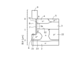
- FIG. 1 is a cross-sectional view showing the structure of a semiconductor device according to an embodiment.
- FIG. 2 is a cross-sectional view schematically showing the vicinity of the channel portion of FIG.
- FIG. 3 is a characteristic diagram showing the impurity concentration profile along the cutting line A-A' in FIG.
- FIG. 4 is a characteristic diagram showing the ion implantation profile of the channel portion of FIG.
- FIG. 5 is a characteristic diagram showing the relationship between the gate threshold voltage and the on-resistance in Examples 1 and 2.
- FIG. FIG. 6 is a cross-sectional view showing the structure of a conventional semiconductor device.
- n or p layers and regions prefixed with n or p mean that electrons or holes are majority carriers, respectively. Also, + and - attached to n and p mean that the impurity concentration is higher and lower than that of the layer or region not attached, respectively.
- the same configurations are denoted by the same reference numerals, and overlapping descriptions are omitted.
- FIG. 1 is a cross-sectional view showing the structure of a semiconductor device according to an embodiment.
- FIG. 2 is a cross-sectional view schematically showing the vicinity of the channel portion in FIG.
- FIG. 3 is a characteristic diagram showing the impurity concentration profile along the cutting line AA' in FIG.
- FIG. 4 is a characteristic diagram showing the ion implantation profile of the channel portion of FIG.
- a semiconductor device 10 according to the embodiment shown in FIG. 1 is a vertical SiC-MOSFET having a trench gate structure on the front surface side of a semiconductor substrate (semiconductor chip) 30 using silicon carbide (SiC) as a semiconductor material. is.
- the semiconductor substrate 30 includes an n ⁇ -type drift region (first semiconductor region) 2 and a p-type base region (second semiconductor region) 3 on the front surface of an n + -type starting substrate 31 using SiC as a semiconductor material. It is an epitaxial substrate formed by laminating respective epitaxial layers (silicon carbide layers) 32 and 33 in this order.
- the semiconductor substrate 30 has a main surface (first main surface) on the p-type epitaxial layer (second conductivity type silicon carbide layer) 33 side, and a main surface on the n + -type starting substrate 31 side (n + -type
- the rear surface of the starting substrate 31) is the rear surface (second main surface).
- the n ⁇ -type epitaxial layer (first conductivity type silicon carbide layer) 32 is doped with an n-type impurity such as nitrogen (N).
- the p-type epitaxial layer 33 is doped with a p-type impurity such as aluminum (Al).
- the n + -type starting substrate 31 is the n + -type drain region 1 .
- the n ⁇ -type drift region 2 is adjacent to the n + -type starting substrate 31 in the depth direction.
- P-type base region 3 is provided between the front surface of semiconductor substrate 30 and n ⁇ -type drift region 2 .
- the trench gate structure is composed of a p-type base region 3 , an n + -type source region (third semiconductor region) 4 , a p ++ -type contact region 5 , a trench 6 , a gate insulating film 7 and a gate electrode 8 .
- a p + -type region (first , 2 high-concentration regions) 21 and 22 and an n-type current diffusion region 23 are selectively provided.
- the p + -type regions 21 and 22 and the n-type current diffusion region 23 are diffusion regions formed inside the n - -type epitaxial layer 32 by ion implantation.
- the p + -type region 21 is provided apart from the p-type base region 3 and faces the bottom surface of the trench 6 in the depth direction.
- the p + -type region 21 is electrically connected to the source electrode 11 by being partially linked to the p + -type region 22 in a portion not shown or linked to another p-type region. .
- the p + -type region 21 may be in contact with the gate insulating film 7 at the bottom surface of the trench 6 or may be separated from the bottom surface of the trench 6 .
- the p + -type region 21 also faces the bottom corners (boundary between the side wall and the bottom) of the trench 6 in the depth direction.
- the electric field applied to the gate insulating film 7 at the corners of the bottom surface of the trench 6 is also alleviated, and the effect of alleviating the electric field near the bottom surface of the trench 6 is enhanced.
- the p + -type regions 22 are provided between the trenches 6 adjacent to each other and separated from the trenches 6 and the p + -type regions 21 .
- the p + -type region 22 is in contact with the p-type base region 3 on the n + -type source region 4 side (the front surface side of the semiconductor substrate 30 ), and is electrically connected to the source electrode 11 through the p-type base region 3 . It is connected to the.
- P + -type regions 21 and 22 are adjacent to each other in a direction parallel to the front surface of semiconductor substrate 30 .
- an n-type electrode formed adjacent to a channel portion 3a described later on a current path of a drift current (main current) flowing in the semiconductor substrate 30 from the drain electrode 12 toward the source electrode 11 is formed. is the JFET portion of .
- the surfaces of the p + -type regions 21 and 22 on the n + -type drain region 1 side are located at approximately the same depth. Approximately the same depth means that the depths are the same within a range including tolerance due to process variations.
- the n-type current spreading region 23 is a so-called current spreading layer (CSL) that reduces spreading resistance of carriers.
- the n-type current diffusion region 23 is provided in contact with the p + -type regions 21 and 22 between the trenches 6 adjacent to each other. Further, the n-type current diffusion region 23 is in contact with the p-type base region 3 on the n + -type source region 4 side surface, and in contact with the n ⁇ -type drift region 2 on the n + -type drain region 1-side surface. It reaches the trench 6 in a direction parallel to the front surface of 30 and contacts the gate insulating film 7 .
- N-type current diffusion region 23 may not be provided.
- the n ⁇ -type drift region 2 extends from the n + -type drain region 1 side to the p-type base region 3 between the adjacent trenches 6. At the same time, it reaches the trench 6 in the direction parallel to the front surface of the semiconductor substrate 30 and comes into contact with the gate insulating film 7 .
- a portion of n ⁇ -type epitaxial layer 32 excluding p + -type regions 21 and 22 and n-type current diffusion region 23 is n ⁇ -type drift region 2 .
- the n + -type source region 4 and the p ++ -type contact region 5 are diffusion regions formed inside the p-type epitaxial layer 33 by ion implantation into the p-type epitaxial layer 33 from the front surface of the semiconductor substrate 30 . be.
- the n + -type source region 4 and the p ++ -type contact region 5 are selectively provided between the front surface of the semiconductor substrate 30 and the p-type base region 3 respectively in contact with the p-type base region 3 . .
- the n + -type source region 4 and the p ++ -type contact region 5 are in ohmic contact with the source electrode 11 on the front surface of the semiconductor substrate 30 .
- the n + -type source region 4 is provided closer to the trench 6 than the p ++ -type contact region 5 and is in contact with the gate insulating film 7 on the side wall of the trench 6 .
- the p ++ type contact region 5 may not be provided. If p ++ -type contact region 5 is not provided, instead of p ++ -type contact region 5 , p-type base region 3 reaches the front surface of semiconductor substrate 30 and contacts source electrode 11 .
- a portion of p-type epitaxial layer 33 excluding n + -type source region 4 and p ++ -type contact region 5 is p-type base region 3 .
- Trench 6 penetrates n + -type source region 4 and p-type base region 3 in the depth direction from the front surface of semiconductor substrate 30 and terminates inside n ⁇ -type epitaxial layer 32 .
- a gate insulating film 7 is provided along the inner wall of trench 6 .
- a gate electrode 8 is provided on the gate insulating film 7 inside the trench 6 . The gate electrode 8 is connected to the n + -type source region 4, the p-type base region 3 and the n-type current diffusion region 23 (n ⁇ It faces the mold drift region 2).
- a channel (n-type inversion layer) is formed in a portion (channel portion: portion surrounded by a broken line) 3a of the p-type base region 3 along the sidewall of the trench 6 when the MOSFET is turned on.
- a p-type impurity such as aluminum (Al) is introduced into the p-type base region 3 by ion implantation in two stages (twice) or more from the front surface of the semiconductor substrate 30 .
- the p-type impurity concentration profile 41 in the depth direction of the p-type base region 3 is optimized by ion implantation in two or more steps (for example, two steps in FIGS. 3 and 4) into the p-type base region 3, resulting in the channel portion 3a. resistance is adjusted.
- the ion implantation in two or more stages into the p-type base region 3 exhibits a relatively low peak concentration at a deeper depth position toward the n + -type drain region 1 side as the acceleration voltage increases.
- Gaussian-distributed ion implantation profiles ion implantation profiles 61 and 62 in FIG. 4 in which the impurity concentration decreases with substantially the same gradient from the depth position toward the n + type source region 4 side and the n + type drain region 1 side, respectively. equivalent to ).
- the conditions for the ion implantation in two or more steps into the p-type base region 3 are, for example, the acceleration voltage and the dose of the ion implantation having the next lowest acceleration voltage after the ion implantation for which the conditions are set, and the acceleration voltage is set to 1.1. It is set within the range of about 3 times or more and 1.6 times or less, and the dose amount is set within the range of about 10% or more and 20% or less.
- the ion implantation with the next highest acceleration voltage after this ion implantation has an acceleration voltage of should be in the range of about 780 keV to 960 keV, and the dose should be in the range of about 1.5 ⁇ 10 12 /cm 2 to 3.0 ⁇ 10 12 /cm 2 .
- a p-type impurity concentration profile 41 in the depth direction of the p-type base region 3 is obtained at the depth positions (corresponding to the depth positions D1 and D2 in FIG. 3) of the ranges of two or more stages of ion implantation with different acceleration voltages.
- the peak concentration of each ion implantation profile is shown, and the peak concentration is relatively lower at a deeper position toward the n + -type drain region 1 side.
- the depth position of the peak concentration of the ion implantation profile of the ion implantation with the lowest acceleration voltage (first depth position: corresponding to the depth position D1 in FIG. 3) is , the impurity concentration of the p-type base region 3 is the highest, and is preferably set closer to the n + -type source region 4 than the center of the p-type base region 3 in the depth direction.
- the p-type impurity concentration profile 41 in the depth direction of the p-type base region 3 is obtained from the depth position of the peak concentration (the peak concentration closest to the n + -type source region 4 side) of the ion implantation profile of ion implantation with the lowest acceleration voltage.
- the impurity concentration decreases toward the n + -type source region 4 side.
- the ion implantation profile on the side of the n + -type source region 4 from the depth position of the peak concentration on the side of the n + -type source region 4 is the most accelerated voltage. It is an ion implantation profile on the n + -type source region 4 side from the depth position of the peak concentration of the ion implantation profile of low ion implantation.
- the depth position of the peak concentration closest to the n + -type source region 4 (corresponding to the depth position D1 in FIG. 3) is closer to the n + -type drain.
- the p-type impurity concentration profile on the region 1 side is the difference between the impurity concentration profile of the p-type epitaxial layer 33 and the ion implantation profile of the ion implantation with the lowest acceleration voltage among the two or more stages of ion implantation into the p-type base region 3 .
- the p-type impurity concentration profile 41 in the depth direction of the p-type base region 3 is the depth of the peak concentration closest to the n + -type source region 4 side. It is asymmetric with respect to the position.
- the acceleration voltage becomes the largest from the depth position of the peak concentration closest to the n + -type source region 4 toward the n + -type drain region 1 side.
- the impurity concentration is low at the depth position (second depth position) of the range of each ion implantation except for the low ion implantation.
- the ion implantation profile on the side of the n + -type drain region 1 from the depth position of the peak concentration on the side of the n + -type drain region 1 is the most accelerated voltage.
- 1 is an ion implantation profile on the n + -type drain region 1 side from the depth position of the peak concentration of the ion implantation profile of high ion implantation.
- the p-type impurity concentration profile 41 in the depth direction of the p-type base region 3 is mountain-like toward the n + -type drain region 1 side between the peak concentrations of the ion implantation profiles adjacent to each other in the depth direction.
- the impurity concentration decreases with a gradient that forms a protruding curve (curve that is convex in the direction in which the impurity concentration increases), or the impurity concentration is uniform (flat without a gradient). That is, the p-type impurity concentration profile 41 in the depth direction of the p-type base region 3 has a valley-like depression between the peak concentrations of the ion implantation profiles adjacent to each other in the depth direction (protruding in the direction in which the impurity concentration decreases). dents) do not occur.
- the peak concentration closest to the n + -type source region 4 in the p-type impurity concentration profile 41 in the depth direction of the p-type base region 3 is, for example, 4.0 ⁇ 10 17 /cm 3 or more and 8.0 ⁇ 10 17 /cm 3 . It is within the range of about 3 or less.
- the depth position of the peak concentration closest to the n + -type source region 4 in the p-type impurity concentration profile 41 in the depth direction of the p-type base region 3 is closer to the n + -type drain region 1 than the n + -type source region 4. set.
- the distance between the n + -type source region 4 and the p-type base region 3 is A distance w1 to the boundary 51 is greater than 0 ⁇ m.
- This distance w1 is, for example, about 10% or more and 30% or less of the channel length L (10% ⁇ w1/L ⁇ 100 ⁇ 30%).
- the channel length L is the length of the channel portion 3a along the side wall of the trench 6, and extends from the boundary 51 between the n + -type source region 4 and the p-type base region 3 to the p-type base region 3 and the n-type current diffusion region. 23 to the boundary 52.
- the distance between the peak concentrations of the ion implantation profiles adjacent to each other in the depth direction of the p-type impurity concentration profile 41 in the depth direction of the p-type base region 3 is the distance between all the peak concentrations is in the range of about 0.1 ⁇ m or more and 0.2 ⁇ m or less.
- the distance to the boundary 52 with the n-type current diffusion region 23 is preferably as wide as possible.
- the n of the p-type base region 3 increases. This is because the impurity concentration on the + type drain region 1 side becomes higher and the distance between the channel portion 3a and the p + type region 21 becomes narrower, so that the current path of the drift current becomes high resistance.
- the p-type base region 103 is implanted in one step to restore the p-type base region 103.
- a p-type impurity concentration profile 141 in the depth direction is adjusted.
- the p-type impurity concentration profile 141 in the depth direction of the p-type base region 103 shows a peak concentration at the depth position of the range of one-stage ion implantation into the p-type base region 103, and the depth of the peak concentration It is a Gaussian distribution in which the impurity concentration decreases with substantially the same gradient from the position D101 toward the n + -type source region 104 side and the n + -type drain region 101 side (see FIG. 3).
- the p-type impurity concentration profile 141 in the depth direction of the p-type base region 103 of the conventional example is symmetrical with respect to the depth position D101 of the peak concentration of one ion implantation profile formed by one stage of ion implantation. , and it is not possible to adjust the p-type impurity concentration profile on only one side of the n + -type source region 104 side and the n + -type drain region 101 side with respect to the depth position D101.
- the conditions for one-stage ion implantation into the p-type base region 103 of the conventional example shown in FIG . (indicated as "Al600 keV" in FIG. 3).
- the p-type impurity concentration profile 41 in the depth direction of the p-type base region 3 is obtained by ion implantation with the lowest acceleration voltage. Only the n + -type drain region 1 side (one side) can be adjusted with respect to the depth position D1 of the peak concentration of the ion implantation profile.
- the ion implantation with the lowest acceleration voltage among the two stages of ion implantation into the p-type base region 3 of Examples 1 and 2 The conditions for ion implantation in the second stage are the same as the conditions for ion implantation in the first stage in the conventional example (shown as "Al600 keV" in FIG. 3).
- the conditions for the remaining one stage of ion implantation are, for example, an acceleration voltage of about 900 keV and a dopant of about 900 keV.
- Aluminum is used, and the dose amount is about 2.0 ⁇ 10 12 /cm 2 (shown as “+Al900 keV — 2 ⁇ 10 12 /cm 2 ” in FIG. 3).
- the ion implantation conditions for the second step in Example 2 are, for example, an acceleration voltage of about 900 keV, a dopant of aluminum, and a dose of about 3.0 ⁇ 10 12 /cm 2 (in FIG. 3, “+Al900 keV — 3 ⁇ 10 12 /cm 2 ”). Examples 1 and 2 are manufactured under the same conditions except that the dose amount of the second-stage ion implantation into the p-type base region 3 is different.
- the p-type impurity concentration profile 41 (41a, 41b) in the depth direction of the p-type base region 3 is obtained by ion implantation in the first stage ion implantation performed under the same ion implantation conditions as in the conventional example.
- the profile 61 shows the peak concentration at the same depth position D1 as the depth position D101 of the peak concentration of the p-type impurity concentration profile 141 of the conventional example.
- the p-type impurity concentration profile 41 (41a, 41b) in the depth direction of the p-type base region 3 is closer to the n + -type drain than the peak concentration depth position D1 closest to the n + -type source region 4 side.
- the peak concentration of the ion implantation profile 62 of the second ion implantation is reached.
- the p-type impurity concentration profile 41 (41a, 41b) in the depth direction of the p-type base region 3 is closer to the n + -type drain region 1 than the peak concentration depth position D1 closest to the n + -type source region 4 side.
- the p-type impurity concentration on the n + -type drain region 1 side is higher than the depth position D101 of the peak concentration of the p-type impurity concentration profile 141 of the conventional example.
- the p-type impurity concentration profile 41 (41b) in the depth direction of the p-type base region 3 has a peak concentration depth closest to the n + -type source region 4 as the dose amount of the second-stage ion implantation increases.
- the p-type impurity concentration on the n + -type drain region 1 side is higher than the position D1.
- the peak concentration closest to the n + -type source region 4 in the p-type impurity concentration profile 41 in the depth direction of the p-type base region 3 is, for example, about 6.0 ⁇ 10 17 /cm 3 .
- the n + -type source region 4 and the p-type base region 3 are the intersections of the n-type impurity concentration profile 42 in the depth direction of the n + -type source region 4 and the p-type impurity concentration profile 41 in the depth direction of the p-type base region 3 .
- FIG. 1 is the boundary 51 between The intersection of the p-type impurity concentration profile 41 (41a, 42b) in the depth direction of the p-type base region 3 and the n-type impurity concentration profile 43 in the depth direction of the n-type current diffusion region 23 is the p-type base region 3 and n It is the boundary 52 (52a, 52b) with the mold current diffusion region 23.
- the n-type impurity concentration profile 42 in the depth direction of the n + -type source region 4 shows a peak concentration at a depth position away from the front surface of the semiconductor substrate 30, and the semiconductor substrate 30 from the depth position of the peak concentration. It has a substantially Gaussian distribution in which the impurity concentration decreases toward the front surface and the n + -type drain region 101 side.
- An n - type impurity concentration profile 42 in the depth direction of the n + -type source region 4 has two or more places where substantially the same peak concentration is achieved by two or more stages of ion implantation with substantially the same dose amount and different acceleration voltages.
- the interval between the peak concentrations of the n-type impurity concentration profile 42 in the depth direction of the n + -type source region 4 may be recessed like a valley (forming a convex curve in the direction in which the impurity concentration decreases).
- An n-type impurity concentration profile 43 in the depth direction of the n-type current diffusion region 23 is a box profile formed by a plurality of steps of ion implantation with substantially the same dose amount and different acceleration voltages. There are as many locations with the same peak concentration as the number of stages of ion implantation.
- the n-type current diffusion region 23 may be recessed like a valley between the peak concentrations of the n-type impurity concentration profile 43 in the depth direction.
- Approximately the same (or approximately uniform) impurity concentration and approximately the same dose amount mean the same impurity concentration and the same dose amount within a range including tolerance due to process variations.
- the n-type impurity concentration profile 43 in the depth direction of the n-type current diffusion region 23 has a peak concentration at the depth position of the range of ion implantation in a plurality of steps, and from the depth position of each peak concentration,
- the Gaussian-distributed ion implantation profile in which the impurity concentration decreases toward the n + -type source region 4 side and the n + -type drain region 1 side is continuous in the depth direction Z and has a wavy shape.
- the impurity concentration decreases from the depth position of the peak concentration closest to the n + -type source region 4 toward the n + -type source region 4 side. It may be.
- a channel portion of the p-type base region 3 is a portion from a boundary 51 between the n + -type source region 4 and the p-type base region 3 to a boundary 52 (52a, 52b) between the p-type base region 3 and the n-type current diffusion region 23. 3a.
- a p-type impurity concentration profile 40 in the depth direction of the p-type epitaxial layer 33 has a uniform impurity concentration of, for example, about 3.5 ⁇ 10 16 /cm 3 .
- Only the channel portion 3a of the p-type base region 3 has the above-described p-type impurity concentration profile 41, and the portion of the p-type base region 3 other than the channel portion 3a is composed only of the p-type epitaxial layer 33 and is uniform in the depth direction. p-type impurity concentration profile.
- the on-resistance is determined by the peak concentration closest to the n + -type source region 4 in the p-type impurity concentration profile 41 in the depth direction of the p-type base region 3 .
- the gate threshold voltage is determined by the impurity concentration of the portion closer to the n + -type drain region 1 than the depth position of the peak concentration on the source region 4 side.
- the gate threshold voltage is increased and the noise resistance is improved, so that erroneous turn-on of the MOSFET can be suppressed.
- the internal resistance of the portion of the p-type base region 3 on the n + -type drain region 1 side is small, so that the on-resistance can be maintained even if the gate threshold voltage is increased. .
- the p-type impurity concentration profile 41 in the depth direction of the p-type base region 3 is gradually decreased from the depth position of the peak concentration closest to the n + -type source region 4 toward the n + -type drain region 1 side.
- the impurity concentration of the p-type base region 3 is, for example, about 0.2 ⁇ m from the depth position of the peak concentration closest to the n + -type source region 4 side of the p-type impurity concentration profile 41 in the depth direction to the n + -type drain region 1 side. 1/10 or more of the peak concentration closest to the n + -type source region 4 in the portion up to the depth position (third depth position).
- the interlayer insulating film 9 is provided over the entire front surface of the semiconductor substrate 30 and covers the gate electrode 8 .
- FIG. 1 shows only one cell (element unit) of the MOSFET, a plurality of cells having the same structure are arranged adjacent to each other on the semiconductor substrate 30 .
- the n + -type source region 4 and the p ++ -type contact region 5 are exposed in the contact hole of the interlayer insulating film 9 .
- the source electrode (first electrode) 11 is in ohmic contact with the front surface of the semiconductor substrate 30 through the contact hole of the interlayer insulating film 9, and is connected to the n + -type source region 4, the p ++ -type contact region 5 and the p-type base. It is electrically connected to region 3 .
- a drain electrode 12 is provided on the entire back surface of the semiconductor substrate 30 .
- the drain electrode (second electrode) 12 is electrically connected to the n + -type drain region 1 through ohmic contact with the n + -type drain region 1 (n + -type starting substrate 31).
- the operation of the semiconductor device 10 will be described. While a voltage lower than the gate threshold voltage is applied to the gate electrode 8 while a positive voltage (forward voltage) is applied to the drain electrode 12 with respect to the source electrode 11, the p + -type regions 21 and 22 and A pn junction (main junction) between the p-type base region 3, the n-type current diffusion region 23, and the n ⁇ -type drift region 2 is reverse-biased, thereby keeping the SiC-MOSFET (semiconductor device 10) in an off state. do.
- a voltage lower than the gate threshold voltage is applied to the gate electrode 8 while a positive voltage (forward voltage) is applied to the drain electrode 12 with respect to the source electrode 11, the p + -type regions 21 and 22 and A pn junction (main junction) between the p-type base region 3, the n-type current diffusion region 23, and the n ⁇ -type drift region 2 is reverse-biased, thereby keeping the SiC-MOSFET (semiconductor device 10) in
- the channel portion 3a along the side wall of the trench 6 of the p-type base region 3 is formed.
- a channel (n-type inversion layer) is formed at .
- a current drift current flows from the n + -type drain region 1 through the channel portion 3a toward the n + -type source region 4, turning on the SiC-MOSFET.
- the portion of the p-type base region 3 on the n + -type drain region 1 side is located inside the peak concentration portion of the p-type impurity concentration profile 41 in the depth direction of the p-type base region 3 closest to the n + -type source region 4 side. resistance is low.
- the portion of the p-type base region 3 on the n + -type drain region 1 side also bears the voltage.
- the impurity concentration determines the gate threshold voltage.
- the portion of the p-type base region 3 on the n + -type drain region 1 side increases.
- voltage burden increases.
- the voltage burden of the peak concentration portion closest to the n + -type source region 4 side of the p-type impurity concentration profile 41 in the depth direction of the p-type base region 3 is reduced. can be reduced.
- the SiC-MOSFET When the SiC-MOSFET is completely turned on, the internal resistance of the portion of the p-type base region 3 on the n + -type drain region 1 side hardly contributes, and the p-type impurity concentration profile in the depth direction of the p-type base region 3 is The voltage is borne only by the peak concentration portion of 41 closest to the n + -type source region 4 side. Therefore, the on-resistance is determined by the peak concentration closest to the n + -type source region 4 in the p-type impurity concentration profile 41 in the depth direction of the p-type base region 3 .
- the p-type impurity concentration profile 41 in the depth direction of the p-type base region 3 gradually decreases from the depth position of the peak concentration closest to the n + -type source region 4 toward the n + -type drain region 1 side. ing. Therefore, even if the gate threshold voltage is increased by increasing the impurity concentration of the portion of the p-type base region 3 on the n + -type drain region 1 side, the variation in the gate threshold voltage is maintained with respect to the target gate threshold voltage value. can do.
- an n ⁇ -type epitaxial layer 32 to be the n ⁇ -type drift region 2 is epitaxially grown (deposited) on the front surface of an n + -type starting substrate (starting wafer) 31 using SiC as a semiconductor material.
- the n ⁇ -type epitaxial layer 32 is epitaxially grown to a thickness smaller than a predetermined thickness after the completion of the product (semiconductor device 10).
- the impurity concentration of the n ⁇ -type epitaxial layer 32 is, for example, about 1 ⁇ 10 16 /cm 3 .
- n + -type regions 21 and p + -type regions 22 are formed in the surface region of the n ⁇ -type epitaxial layer 32 so as to be alternately and repeatedly arranged apart from each other. and a lower portion (portion on the n + -type drain region 1 side) are selectively formed.
- an n - type current diffusion region 23 is formed between the p + -type region 21 and the p + -type region 22 adjacent to each other in the surface region of the n - -type epitaxial layer 32. form the lower part.
- epitaxial growth is further performed to thicken the n ⁇ -type epitaxial layer 32 to a predetermined thickness.
- the upper portion of the p + -type region 22 portion on the n + -type source region 4 side
- the upper part of the n - type current diffusion region 23 is formed between the adjacent p + -type regions 22 in the portion where the thickness of the n ⁇ -type epitaxial layer 32 is increased.
- An upper portion of the p + -type region 22 and an upper portion of the n-type current diffusion region 23 are provided with an n ⁇ -type epitaxial layer at a position facing the lower portion of the p + -type region 22 and the lower portion of the n-type current diffusion region 23 in the depth direction, respectively.
- a thickened portion 32 is formed with a penetrating depth to connect the bottom of the p + -type region 22 and the bottom of the n-type current spreading region 23 .
- a portion of the n ⁇ -type epitaxial layer 32 closer to the n + -type starting substrate 31 than the p + -type regions 21 and 22 and the n - type current diffusion region 23 becomes the n ⁇ -type drift region 2 .
- a p-type epitaxial layer 33 to be the p-type base region 3 is epitaxially grown (deposited) to a thickness of, for example, about 1 ⁇ m.
- a semiconductor substrate (semiconductor wafer) 30 having epitaxial layers 32 and 33 laminated in order on the front surface of the n + -type starting substrate 31 is fabricated (manufactured) (first step).
- the n + -type source region 4 and the p ++ -type contact region 5 are selectively formed in the surface region of the p-type epitaxial layer 33 (third step).
- a portion of p-type epitaxial layer 33 closer to n ⁇ -type epitaxial layer 32 than n + -type source region 4 and p ++ -type contact region 5 serves as p-type base region 3 .
- the p-type impurity concentration profile 41 in the depth direction of the p-type base region 3 is adjusted by two or more stages of ion implantation from the front surface of the semiconductor substrate 30 into the p-type base region 3 (second step). ).
- the two or more stages of ion implantation into the p-type base region 3 are set at different acceleration voltages at different depths within the p-type base region 3, and the higher the acceleration voltage, the lower the dose. do.
- the ion implantation in two or more stages (two stages in FIG. 4) into the p-type base region 3 is such that the higher the acceleration voltage of the ion implantation, the deeper the position toward the n + -type drain region 1 side. (Depth positions D1 and D2 in FIG. 4) and an ion implantation profile with a wide half width (ion implantation profiles 61 and 62 in FIG. 4) are formed. Ion implantation profiles formed by two or more stages of ion implantation into p-type base region 3 and adjacent in the depth direction may be adjacent in the depth direction or may overlap each other in the depth direction.
- the ion implantation profile of the ion implantation into the p-type base region 3 preferably does not reach the n-type current diffusion region 23.
- the ion implantation profile of the ion implantation into the p-type base region 3 with the highest acceleration voltage ( 4) should be terminated at the boundary between the p-type epitaxial layer 33 and the n ⁇ -type epitaxial layer 32 .
- the peak concentration of the ion implantation profile by ion implantation with the lowest acceleration voltage into the p-type base region 3 (that is, the maximum n + -type of the p-type impurity concentration profile 41 in the depth direction of the p-type base region 3)
- the on-resistance is determined by the peak concentration on the source region 4 side.
- the gate threshold voltage is determined by the impurity concentration of the portion on the 1 side.
- the p-type impurity concentration profile 41 in the depth direction of the p-type base region 3 gradually decreases from the depth position of the peak concentration closest to the n + -type source region 4 toward the n + -type drain region 1 side. are doing.
- the p-type impurity concentration profile 41 in the depth direction of the p-type base region 3 has the n The impurity concentration on the n + type drain region 1 side is higher than the depth position of the peak concentration on the + type source region 4 side.
- the order of two or more stages of ion implantation into the p-type base region 3 can be appropriately changed.
- the introduced impurities may be forced into a deep portion of the semiconductor substrate 30 by subsequent ion implantation with a high acceleration voltage. Therefore, it is easier to adjust the p-type impurity concentration profile 41 in the depth direction of the p-type base region 3 to the target p-type impurity concentration profile by performing ion implantation in order from the highest acceleration voltage.
- the p-type base region 3 has the above-described p-type impurity concentration profile 41 in the depth direction.
- the p-type impurity concentration profile 41 may be formed by introducing p-type impurities into the formation region of the p-type base region 3 by two or more stages of ion implantation.
- an n + -type source region 4 and a p ++ -type contact region 5 are each selectively formed in the surface region of the n-type epitaxial layer in contact with the p-type base region 3 .
- the order of adjustment (or formation) of the p-type impurity concentration profile 41 in the depth direction of the p-type base region 3, formation of the n + -type source region 4, and formation of the p ++- type contact region 5 is appropriately changed. It is possible.
- heat treatment is performed to activate all the ion-implanted impurities.
- a trench 6, a gate insulating film 7, a gate electrode 8, an interlayer insulating film 9, a source electrode 11 and a drain electrode 12 are formed by a general method (fourth to seventh steps). Thereafter, the semiconductor wafer (semiconductor substrate 30) is diced (cut) into individual chips, thereby completing the semiconductor device 10 shown in FIG.
- the p-type impurity profile in the depth direction of the p-type base region is adjusted by two or more stages of ion implantation, and the peak concentration on the n + -type source region side is the highest. It gradually decreases from the depth position toward the n + -type drain region side. Since the internal resistance of the portion of the p-type base region on the n + -type drain region side is reduced by ion implantation at a high acceleration voltage, the impurity concentration of the portion of the p-type base region on the n + -type drain region side is increased to lower the gate threshold. Even if the voltage is increased, the on-resistance does not increase. Alternatively, the on-resistance can be reduced while maintaining the gate threshold voltage. Therefore, it is possible to improve the trade-off relationship between increasing the gate threshold voltage and reducing the on-resistance.
- FIG. 5 is a characteristic diagram showing the relationship between the gate threshold voltage and the on-resistance in Examples 1 and 2.
- FIG. The horizontal axis of FIG. 5 is the gate threshold voltage Vth [V]
- the vertical axis is the on-resistance RonA [m ⁇ cm 2 ].
- FIG. 5 shows the relationship between the gate threshold voltage Vth and the on-resistance RonA for the first and second embodiments and the conventional example.
- the gate threshold voltage Vth can be made higher than in the conventional example when the on-resistance RonA is the same as in the conventional example.
- the on-resistance RonA is reduced more than the conventional example while maintaining the variation of the gate threshold voltage Vth with respect to the target gate threshold voltage value to the same extent as the conventional example. was confirmed to be possible.
- the gate threshold voltage Vth can be increased and the on-resistance RonA can be reduced. It was confirmed that the trade-off relationship between reduction and reduction can be improved. Therefore, even if the gate threshold voltage Vth is increased, the vertical SiC-MOSFET having the trench gate structure can have a structure in which the on-resistance does not increase.
- the present invention can be modified in various ways, and in the above-described embodiment, for example, the dimensions and impurity concentration of each part are set variously according to the required specifications.
- the first conductivity type is n-type and the second conductivity type is p-type in the embodiments
- the present invention can be similarly applied even if the first conductivity type is p-type and the second conductivity type is n-type. .
- the semiconductor device and the method for manufacturing a semiconductor device according to the present invention are useful for power semiconductor devices used in power converters and power supply devices for various industrial machines.
- Source electrode 12 Drain electrode 21, 22 p + -type region 23 n-type current diffusion region 30 semiconductor substrate 31 n + -type starting substrate 32 n - -type epitaxial layer 33 p-type epitaxial layer 40, 41, 41a, 41b p-type impurity concentration profile 42, 43 n-type impurity concentration profile 51 boundary between n + -type source region and p-type base region 52 boundary between p-type base region and n-type current diffusion region 61, 62 ion implantation profile D1, D2 peak of ion implantation profile Concentration depth position L Channel length
Landscapes
- Junction Field-Effect Transistors (AREA)
Priority Applications (3)
| Application Number | Priority Date | Filing Date | Title |
|---|---|---|---|
| JP2023578422A JP7750312B2 (ja) | 2022-02-02 | 2022-12-23 | 半導体装置および半導体装置の製造方法 |
| CN202280051873.8A CN117716514A (zh) | 2022-02-02 | 2022-12-23 | 半导体装置以及半导体装置的制造方法 |
| US18/427,607 US20240213307A1 (en) | 2022-02-02 | 2024-01-30 | Semiconductor device and method of manufacturing semiconductor device |
Applications Claiming Priority (2)
| Application Number | Priority Date | Filing Date | Title |
|---|---|---|---|
| JP2022-015237 | 2022-02-02 | ||
| JP2022015237 | 2022-02-02 |
Related Child Applications (1)
| Application Number | Title | Priority Date | Filing Date |
|---|---|---|---|
| US18/427,607 Continuation US20240213307A1 (en) | 2022-02-02 | 2024-01-30 | Semiconductor device and method of manufacturing semiconductor device |
Publications (1)
| Publication Number | Publication Date |
|---|---|
| WO2023149131A1 true WO2023149131A1 (ja) | 2023-08-10 |
Family
ID=87552268
Family Applications (1)
| Application Number | Title | Priority Date | Filing Date |
|---|---|---|---|
| PCT/JP2022/047790 Ceased WO2023149131A1 (ja) | 2022-02-02 | 2022-12-23 | 半導体装置および半導体装置の製造方法 |
Country Status (4)
| Country | Link |
|---|---|
| US (1) | US20240213307A1 (https=) |
| JP (1) | JP7750312B2 (https=) |
| CN (1) | CN117716514A (https=) |
| WO (1) | WO2023149131A1 (https=) |
Families Citing this family (1)
| Publication number | Priority date | Publication date | Assignee | Title |
|---|---|---|---|---|
| JP6981890B2 (ja) * | 2018-01-29 | 2021-12-17 | ルネサスエレクトロニクス株式会社 | 半導体装置 |
Citations (4)
| Publication number | Priority date | Publication date | Assignee | Title |
|---|---|---|---|---|
| JP2017139441A (ja) * | 2016-02-01 | 2017-08-10 | 富士電機株式会社 | 炭化珪素半導体装置および炭化珪素半導体装置の製造方法 |
| US20200098868A1 (en) * | 2018-09-20 | 2020-03-26 | Infineon Technologies Ag | Semiconductor Device Including Trench Gate Structure and Manufacturing Method |
| JP2020119945A (ja) * | 2019-01-21 | 2020-08-06 | 富士電機株式会社 | 半導体装置および半導体装置の製造方法 |
| JP2020205295A (ja) * | 2019-06-14 | 2020-12-24 | 国立研究開発法人産業技術総合研究所 | 炭化珪素半導体装置 |
-
2022
- 2022-12-23 JP JP2023578422A patent/JP7750312B2/ja active Active
- 2022-12-23 CN CN202280051873.8A patent/CN117716514A/zh active Pending
- 2022-12-23 WO PCT/JP2022/047790 patent/WO2023149131A1/ja not_active Ceased
-
2024
- 2024-01-30 US US18/427,607 patent/US20240213307A1/en active Pending
Patent Citations (4)
| Publication number | Priority date | Publication date | Assignee | Title |
|---|---|---|---|---|
| JP2017139441A (ja) * | 2016-02-01 | 2017-08-10 | 富士電機株式会社 | 炭化珪素半導体装置および炭化珪素半導体装置の製造方法 |
| US20200098868A1 (en) * | 2018-09-20 | 2020-03-26 | Infineon Technologies Ag | Semiconductor Device Including Trench Gate Structure and Manufacturing Method |
| JP2020119945A (ja) * | 2019-01-21 | 2020-08-06 | 富士電機株式会社 | 半導体装置および半導体装置の製造方法 |
| JP2020205295A (ja) * | 2019-06-14 | 2020-12-24 | 国立研究開発法人産業技術総合研究所 | 炭化珪素半導体装置 |
Also Published As
| Publication number | Publication date |
|---|---|
| CN117716514A (zh) | 2024-03-15 |
| US20240213307A1 (en) | 2024-06-27 |
| JPWO2023149131A1 (https=) | 2023-08-10 |
| JP7750312B2 (ja) | 2025-10-07 |
Similar Documents
| Publication | Publication Date | Title |
|---|---|---|
| US11888047B2 (en) | Lateral transistors and methods with low-voltage-drop shunt to body diode | |
| CN111384179B (zh) | 碳化硅半导体装置及碳化硅半导体装置的制造方法 | |
| CN101083284B (zh) | 具有槽电荷补偿区的半导体器件及方法 | |
| US20070075362A1 (en) | Self-aligned schottky-barrier clamped trench DMOS transistor structure and its manufacturing methods | |
| US20110042727A1 (en) | MOSFET device with reduced breakdown voltage | |
| US20220209004A1 (en) | Semi-SGT MOSFET Device and Method for Making the Same | |
| TWI289355B (en) | Trench MOSFET and method of manufacturing same | |
| JP4990458B2 (ja) | 自己整合されたシリコンカーバイトlmosfet | |
| JP2019129300A (ja) | 半導体装置とその製造方法 | |
| CN107819025B (zh) | 半导体装置和半导体装置的制造方法 | |
| WO2023149131A1 (ja) | 半導体装置および半導体装置の製造方法 | |
| JP2003518749A (ja) | ゲートのブレークダウン保護機能付きのシリコンカーバイトlmosfet | |
| JP2006140250A (ja) | 半導体装置及びその製造方法 | |
| US20240234495A1 (en) | Gate trench power semiconductor devices having self-aligned trench shielding regions and related methods | |
| JP5014622B2 (ja) | 絶縁ゲート型半導体装置の製造方法 | |
| US20030006483A1 (en) | Short channel power MOSFET with increased breakdown voltage | |
| CN119743991A (zh) | 具有bsg侧壁的沟槽超结mosfet的结构及工艺方法 | |
| CN117497418A (zh) | 超结mosfet元胞结构的工艺方法 | |
| CN113437151A (zh) | 电子器件 | |
| HK1114947B (en) | Semiconductor device having trench charge compensation regions and method | |
| HK1114946A1 (en) | Semiconductor device having sub-surface trench charge compensation regions and method | |
| HK1114946B (en) | Semiconductor device having sub-surface trench charge compensation regions and method |
Legal Events
| Date | Code | Title | Description |
|---|---|---|---|
| 121 | Ep: the epo has been informed by wipo that ep was designated in this application |
Ref document number: 22925033 Country of ref document: EP Kind code of ref document: A1 |
|
| WWE | Wipo information: entry into national phase |
Ref document number: 202280051873.8 Country of ref document: CN |
|
| WWE | Wipo information: entry into national phase |
Ref document number: 2023578422 Country of ref document: JP |
|
| NENP | Non-entry into the national phase |
Ref country code: DE |
|
| 122 | Ep: pct application non-entry in european phase |
Ref document number: 22925033 Country of ref document: EP Kind code of ref document: A1 |