WO2023140100A1 - 半導体装置、電子機器および半導体装置の製造方法 - Google Patents
半導体装置、電子機器および半導体装置の製造方法 Download PDFInfo
- Publication number
- WO2023140100A1 WO2023140100A1 PCT/JP2022/048692 JP2022048692W WO2023140100A1 WO 2023140100 A1 WO2023140100 A1 WO 2023140100A1 JP 2022048692 W JP2022048692 W JP 2022048692W WO 2023140100 A1 WO2023140100 A1 WO 2023140100A1
- Authority
- WO
- WIPO (PCT)
- Prior art keywords
- substrate
- semiconductor device
- space
- cavity
- image sensor
- Prior art date
- Legal status (The legal status is an assumption and is not a legal conclusion. Google has not performed a legal analysis and makes no representation as to the accuracy of the status listed.)
- Ceased
Links
Images







Classifications
-
- H—ELECTRICITY
- H10—SEMICONDUCTOR DEVICES; ELECTRIC SOLID-STATE DEVICES NOT OTHERWISE PROVIDED FOR
- H10F—INORGANIC SEMICONDUCTOR DEVICES SENSITIVE TO INFRARED RADIATION, LIGHT, ELECTROMAGNETIC RADIATION OF SHORTER WAVELENGTH OR CORPUSCULAR RADIATION
- H10F39/00—Integrated devices, or assemblies of multiple devices, comprising at least one element covered by group H10F30/00, e.g. radiation detectors comprising photodiode arrays
- H10F39/80—Constructional details of image sensors
- H10F39/804—Containers or encapsulations
-
- H—ELECTRICITY
- H10—SEMICONDUCTOR DEVICES; ELECTRIC SOLID-STATE DEVICES NOT OTHERWISE PROVIDED FOR
- H10F—INORGANIC SEMICONDUCTOR DEVICES SENSITIVE TO INFRARED RADIATION, LIGHT, ELECTROMAGNETIC RADIATION OF SHORTER WAVELENGTH OR CORPUSCULAR RADIATION
- H10F39/00—Integrated devices, or assemblies of multiple devices, comprising at least one element covered by group H10F30/00, e.g. radiation detectors comprising photodiode arrays
- H10F39/011—Manufacture or treatment of image sensors covered by group H10F39/12
- H10F39/014—Manufacture or treatment of image sensors covered by group H10F39/12 of CMOS image sensors
-
- H—ELECTRICITY
- H10—SEMICONDUCTOR DEVICES; ELECTRIC SOLID-STATE DEVICES NOT OTHERWISE PROVIDED FOR
- H10F—INORGANIC SEMICONDUCTOR DEVICES SENSITIVE TO INFRARED RADIATION, LIGHT, ELECTROMAGNETIC RADIATION OF SHORTER WAVELENGTH OR CORPUSCULAR RADIATION
- H10F39/00—Integrated devices, or assemblies of multiple devices, comprising at least one element covered by group H10F30/00, e.g. radiation detectors comprising photodiode arrays
- H10F39/10—Integrated devices
- H10F39/12—Image sensors
- H10F39/18—Complementary metal-oxide-semiconductor [CMOS] image sensors; Photodiode array image sensors
- H10F39/182—Colour image sensors
-
- H—ELECTRICITY
- H10—SEMICONDUCTOR DEVICES; ELECTRIC SOLID-STATE DEVICES NOT OTHERWISE PROVIDED FOR
- H10F—INORGANIC SEMICONDUCTOR DEVICES SENSITIVE TO INFRARED RADIATION, LIGHT, ELECTROMAGNETIC RADIATION OF SHORTER WAVELENGTH OR CORPUSCULAR RADIATION
- H10F39/00—Integrated devices, or assemblies of multiple devices, comprising at least one element covered by group H10F30/00, e.g. radiation detectors comprising photodiode arrays
- H10F39/80—Constructional details of image sensors
- H10F39/811—Interconnections
-
- H—ELECTRICITY
- H10—SEMICONDUCTOR DEVICES; ELECTRIC SOLID-STATE DEVICES NOT OTHERWISE PROVIDED FOR
- H10W—GENERIC PACKAGES, INTERCONNECTIONS, CONNECTORS OR OTHER CONSTRUCTIONAL DETAILS OF DEVICES COVERED BY CLASS H10
- H10W40/00—Arrangements for thermal protection or thermal control
- H10W40/10—Arrangements for heating
-
- H—ELECTRICITY
- H10—SEMICONDUCTOR DEVICES; ELECTRIC SOLID-STATE DEVICES NOT OTHERWISE PROVIDED FOR
- H10W—GENERIC PACKAGES, INTERCONNECTIONS, CONNECTORS OR OTHER CONSTRUCTIONAL DETAILS OF DEVICES COVERED BY CLASS H10
- H10W76/00—Containers; Fillings or auxiliary members therefor; Seals
- H10W76/10—Containers or parts thereof
Definitions
- the present disclosure relates to semiconductor devices, electronic devices, and methods of manufacturing semiconductor devices.
- a semiconductor device equipped with an imaging element such as a CMOS image sensor, a logic IC having a predetermined circuit structure, or a semiconductor element (semiconductor chip) such as a light-emitting element such as a semiconductor laser
- an imaging element such as a CMOS image sensor, a logic IC having a predetermined circuit structure, or a semiconductor element (semiconductor chip) such as a light-emitting element such as a semiconductor laser
- a semiconductor device having a structure in which the semiconductor element is adhered to a substrate such as an organic substrate or a ceramic substrate with a die bonding material forming an adhesive layer.
- a semiconductor element is electrically connected to a substrate by a connecting member such as a bonding wire.
- a transparent member such as glass is provided above the imaging element via a frame-like support member or the like with respect to the substrate (see, for example, Japanese Patent Application Laid-Open No. 2002-200013).
- a configuration is adopted in which the die bonding material is placed partially, not entirely, on the back side of the semiconductor chip.
- a configuration is generally used in which a die bonding material is arranged along the outer shape of a rectangular chip on the back surface of the semiconductor chip, along the periphery of the semiconductor chip.
- the die bonding material is arranged so as to form a rectangular frame shape in plan view. Therefore, a cavity surrounded by the die bonding material exists between the substrate and the semiconductor element, that is, on the back side of the semiconductor element. In such a configuration, the heat of the semiconductor element that generates heat due to its operation is conducted to the substrate side through the die bonding material.
- An object of the present technology is to provide a semiconductor device, an electronic device, and a method of manufacturing a semiconductor device that can improve the thermal conductivity from the semiconductor element to the substrate side and obtain the stability of the heat dissipation characteristics.
- a semiconductor device includes a substrate, a semiconductor element provided on the substrate, and a fluid heat-conducting member filled in a space between the substrate and the semiconductor element, and the substrate is formed with one or more in-substrate cavities that communicate with the space at one end thereof and receive the heat-conducting member.
- the inner-substrate cavity is formed so that the other end side opens toward the surface of the substrate, and the front-surface side of the substrate is provided with a closing portion that closes the other end side of the inner-substrate cavity.
- the closing portion is a supporting member for supporting a transparent member provided for the semiconductor element on the substrate or a joining portion of the transparent member to the surface of the substrate.
- the semiconductor device includes a sealing resin portion formed around the semiconductor element on the substrate, and the closing portion is the sealing resin portion.
- the inner-substrate hollow portion includes a passage portion having a relatively narrow flow passage area and a housing portion communicating with the passage portion and having a larger flow passage area than the passage portion.
- the hollow portion in the substrate is formed so as to form unevenness in a side cross-sectional view of the substrate.
- the cavity in the substrate has, at an end portion on the other end side, an enlarged portion that opens toward the surface of the substrate.
- the semiconductor device further includes a supporting portion that supports the semiconductor element with respect to the substrate and forms the space portion together with the substrate and the semiconductor element, and the substrate has a protrusion that is provided along the inner side of the supporting portion and protrudes from the surface of the substrate.
- the protrusion is provided as part of the substrate.
- An electronic device includes a substrate, a semiconductor element provided on the substrate, and a fluid heat-conducting member filled in a space between the substrate and the semiconductor element, and a semiconductor device in which one or more in-substrate cavities are formed in the substrate such that one end thereof communicates with the space and receives the heat-conducting member.
- a method for manufacturing a semiconductor device includes a step of providing, on a substrate having an inner cavity portion of the substrate with one end side and the other end side thereof open facing the surface side, a die bonding material serving as a supporting portion forming a space communicating with one end side of the inner cavity portion of the substrate together with the substrate and a semiconductor element provided on the substrate so as to form an endless shape in a plan view; placing the semiconductor element on the die bonding material to form the space, and filling the space with the heat conductive member.
- a method for manufacturing a semiconductor device according to the present technology is the method for manufacturing a semiconductor device, further comprising a step of closing an opening on the other end side of the hollow portion in the substrate after the step of filling the heat conductive member.
- the step of closing the opening on the other end side is a step of providing, on the substrate, a transparent member provided for the semiconductor element or a support member for supporting the transparent member on the substrate.
- the step of closing the opening on the other end side is a step of providing a sealing resin portion around the semiconductor element on the substrate.
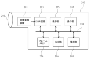
- FIG. 1 is a block diagram showing a configuration example of an electronic device including a semiconductor device according to an embodiment of the present technology
- This technology aims to improve the cooling efficiency of a semiconductor device by filling a heat conductive member (heat conductive liquid) in a space portion on the back side of a semiconductor element on a substrate.
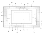
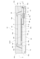
- FIG. 1 A configuration example of a semiconductor device according to a first embodiment of the present technology will be described with reference to FIGS. 1 and 2.
- FIG. 2 a solid-state imaging device including a solid-state imaging device, which is an example of a semiconductor element, will be described as an example of a semiconductor device.
- the up-down direction in FIG. 1 is the up-down direction of the solid-state imaging device 1 .
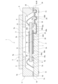
- FIG. 2 is a cross-sectional view taken along the line AA, omitting a part of the configuration in FIG.
- the solid-state imaging device 1 includes a substrate 2 and an image sensor 3 as a solid-state imaging device provided on the substrate 2 .
- the solid-state imaging device 1 also includes a frame 4 as a supporting member provided on the substrate 2 and a glass 5 as a transparent member provided on the frame 4 .
- the image sensor 3 is adhered to the substrate 2 with a die bonding material 6 made of an insulating or conductive adhesive or the like. That is, the solid-state imaging device 1 has a die bonding material 6 that supports the image sensor 3 with respect to the substrate 2 .
- the die bonding material 6 is a supporting portion (element supporting portion) that forms a space portion 7 together with the substrate 2 and the image sensor 3 .
- the solid-state imaging device 1 has a package structure in which a glass 5 is mounted on a substrate 2 via a frame 4 and a cavity 8 as a hollow portion is formed between the image sensor 3 and the glass 5 . That is, a glass 5 is provided above the image sensor 3 in parallel with the image sensor 3 , and the frame 4 and the glass 5 together with the substrate 2 form a cavity 8 which is a closed space on the substrate 2 .
- the substrate 2 is a plate-like member having a rectangular plate-like outer shape.
- the substrate 2 has a front surface 2a on which the image sensor 3 is mounted, a back surface 2b on the opposite side, and four side surfaces 2c.
- An image sensor 3 is die-bonded to the surface 2 a of the substrate 2 with a die-bonding material 6 . That is, the die bonding material 6 provided on the surface 2a of the substrate 2 supports the image sensor 3 so as to face the substrate 2 in parallel with the surface 2a.
- the thickness direction of the substrate 2 is the vertical direction in the solid-state imaging device 1, with the front surface 2a side being the upper side and the back surface 2b side being the lower side.
- the substrate 2 is, for example, a ceramic substrate made of ceramics such as alumina (Al 2 O 3 ), aluminum nitride (AlN), silicon nitride (Si 3 N 4 ), and the like, and is a circuit substrate on which a predetermined circuit pattern is formed by a metal material.
- the substrate 2 may be another type of substrate such as an organic substrate using an organic material such as glass epoxy resin, which is a type of fiber-reinforced plastic, as a base material.
- the image sensor 3 is a semiconductor element including a semiconductor substrate made of silicon (Si), which is an example of a semiconductor.
- the image sensor 3 is a rectangular plate-shaped chip, and the front surface 3a, which is the upper plate surface, is the light receiving surface side, and the opposite plate surface is the back surface 3b.
- the image sensor 3 has four side surfaces 3c.
- a plurality of light receiving elements (photoelectric conversion elements) are formed on the surface 3a side of the image sensor 3 .
- the image sensor 3 is a CMOS (Complementary Metal Oxide Semiconductor) type image sensor.
- the image sensor 3 may be another imaging element such as a CCD (Charge Coupled Device) type image sensor.
- CCD Charge Coupled Device
- the image sensor 3 has, on the surface 3a side, a pixel region 12 including a large number of pixels 11 formed in a predetermined array such as a Bayer array, for example, as a light-receiving portion.
- a predetermined peripheral circuit is formed in the peripheral region 13 .
- the pixel 11 has a photodiode as a photoelectric conversion unit having a photoelectric conversion function and a plurality of pixel transistors.
- a color filter and an on-chip lens are formed corresponding to each pixel 11 on the semiconductor substrate via an antireflection film made of an oxide film or the like, a planarizing film made of an organic material, or the like.
- Light incident on the on-chip lens is received by a photodiode through a color filter, a planarization film, or the like.
- the configuration of the image sensor 3 according to the present technology is not particularly limited.
- the configuration of the image sensor 3 includes, for example, a front side illumination type in which the pixel area 12 is formed on the front surface side of the semiconductor substrate, a back side illumination type in which photodiodes and the like are reversely arranged to improve light transmittance and the back side of the semiconductor substrate is the light receiving surface side, and a single chip in which the peripheral circuits of the pixel group are stacked.
- the die-bonding material 6 is partially interposed between the front surface 2a of the substrate 2 and the back surface 3b of the image sensor 3, and by bonding the substrate 2 and the image sensor 3 in a spaced-apart manner, a space 7, which is a closed space, is formed between the substrate 2 and the image sensor 3.
- the die bonding material 6 functions as a sealing portion that hermetically seals the periphery of the space portion 7 between the substrate 2 and the image sensor 3 . That is, the image sensor 3 is provided on the substrate 2 with the closed space 7 interposed therebetween.
- the die-bonding material 6 is provided at a position corresponding to the peripheral region 13 of the image sensor 3 so as to surround the forming region of the pixel region 12 of the image sensor 3 in plan view.
- the die bonding material 6 is provided along the entire periphery of the image sensor 3 in plan view, and is endlessly formed to have a rectangular frame shape in plan view. Therefore, the die bonding material 6 has four side portions 6 a along each side of the rectangular outer shape of the image sensor 3 .
- the die bonding material 6 is provided at a position within the outline of the image sensor 3 so as to follow the outer edge of the image sensor 3 in plan view.
- the die bonding material 6 is provided at a slightly inner position with respect to the side surface 3 c of the image sensor 3 .
- the die bonding material 6 may be provided so that the outer surface 6c thereof is substantially flush with the side surface 3c of the image sensor 3.
- the die bonding material 6 is made of an insulating material.
- the material forming the die bonding material 6 is, for example, a photosensitive adhesive such as a UV (ultraviolet) curable resin that is an acrylic resin, a thermosetting resin such as an epoxy resin, or a mixture thereof.
- the die bonding material 6 is formed on the front surface 2a of the substrate 2 or the back surface 3b of the image sensor 3 by coating with a dispenser, patterning using photolithography, or the like.
- the die bonding material 6 is an example of the supporting portion according to the present technology, and the material and configuration of the supporting portion according to the present technology are not limited to the present embodiment.
- the support portion according to the present technology may be a portion provided by, for example, attaching a frame-shaped structure made of ceramics such as glass or an inorganic material such as metal or silicon to the substrate 2 and the image sensor 3 with an adhesive or the like.
- the substrate 2 and the image sensor 3 are electrically connected by a plurality of bonding wires 9 as connection members.
- the bonding wire 9 is a conductive wire, for example, has an upwardly convex curved or bent shape such as an arch shape, and is provided so as to straddle between the surface 3 a of the image sensor 3 and the surface 2 a of the substrate 2 .
- the bonding wires 9 are thin metal wires made of, for example, Au (gold), Cu (copper), Al (aluminum), or the like.
- the bonding wire 9 has one end connected to an electrode (not shown) formed on the surface 2a of the substrate 2 and the other end connected to a pad electrode 14 formed on the surface 3a of the image sensor 3, thereby electrically connecting these electrodes.
- a plurality of bonding wires 9 are provided according to the number of pad electrodes 14 .
- the pad electrode 14 is a terminal for transmitting/receiving a signal to/from the image sensor 3, and is formed of an aluminum material or the like using plating or the like.
- the pad electrode 14 is located above the die bonding material 6, for example.
- the electrodes of the substrate 2 to which the bonding wires 9 are connected are electrically connected to a plurality of terminal electrodes 15 formed on the rear surface 2b side of the substrate 2 via predetermined wiring portions formed within the substrate 2.
- terminal electrode 15 for example, a solder ball serving as an external connection terminal is provided to form a BGA (ball grid array).
- the frame 4 is provided on the surface 2a side of the substrate 2 so as to surround the image sensor 3.
- the frame 4 is an integral member made of, for example, a resin material such as epoxy resin, a metal material such as stainless steel or copper (Cu), or ceramics.
- the frame 4 is made of a low-reflection black resin material obtained by adding a black pigment such as carbon black or titanium black to a resin such as liquid crystal polymer or PEEK (polyetheretherketone), and is manufactured by a known method such as injection molding.
- the frame 4, for example, is not limited to being entirely made of one type of material, and may be of a composite structure having a portion made of a metal material and a portion made of a resin material.
- the frame 4 is a rectangular or square frame-shaped member that is larger than the image sensor 3 in plan view and has substantially the same outer dimensions as the substrate 2 in plan view.
- the frame 4 has a plate-like upper surface portion 4b forming an upper surface 4a along a horizontal plane, and a peripheral wall portion 4c formed below the upper surface portion 4b.
- the upper surface portion 4 b is provided in parallel with the image sensor 3 at a position above the image sensor 3 .
- the peripheral wall portion 4 c is formed on the outer edge of the frame 4 along the outer shape of the frame 4 over the entire circumference.
- the lower end surface of the peripheral wall portion 4c forms a lower surface 4d along the horizontal plane.
- the frame 4 has an outer side surface 4e along the vertical direction formed by the upper surface portion 4b and the peripheral wall portion 4c.
- the frame 4 is provided so that four side surfaces 4 e are flush with the side surfaces 2 c of the substrate 2 .
- An inner wall surface of the peripheral wall portion 4c is an inclined surface 4f that is inclined in a direction from the outside toward the inside (center side of the plane) from the lower side to the upper side in a side sectional view. That is, the four slanted surfaces 4f are slanted along the side surfaces of the quadrilateral trapezoidal shape.
- a space for arranging the bonding wires 9 and the like is secured in the cavity 8 by the inclined surface 4f.
- the frame 4 has a rectangular opening 4g penetrating vertically in the center of the upper surface 4b.
- the opening 4g is formed by four inner side surfaces 4h corresponding to the outer shape of the frame 4 in plan view.
- the outer dimensions of the opening 4g in plan view are smaller than the outer shape of the image sensor 3 in plan view.
- the frame 4 is provided with respect to the image sensor 3 so that the entire pixel region 12 is positioned within the aperture range of the aperture 4g in plan view. In plan view, the periphery of the image sensor 3 is located outside the opening range of the opening 4g.
- the frame 4 is provided with the lower surface 4d located outside the electrodes to which the bonding wires 9 are connected with respect to the surface 2a of the substrate 2 so as not to interfere with the bonding wires 9 and the electrodes on the surface 2a of the substrate 2.
- the frame 4 is fixed on the surface 2a of the substrate 2 by a joint portion 16 formed of an adhesive such as an epoxy resin adhesive or an acrylic resin adhesive.
- the upper surface 4 a of the frame 4 serves as a surface for supporting the glass 5 .
- the glass 5 is an example of a transparent member, and is provided to the image sensor 3 via the frame 4.
- the glass 5 has a rectangular plate-like outer shape and has outer dimensions larger than those of the image sensor 3 .
- the glass 5 has a top surface 5 a and a bottom surface 5 b opposite to the other plate surface facing the image sensor 3 .
- the glass 5 is provided on the light receiving surface side of the image sensor 3 so as to be parallel to the image sensor 3 and at a predetermined interval.
- the glass 5 is fixed to the upper surface 4a of the frame 4 with an adhesive such as UV (ultraviolet) curable resin.
- the glass 5 has outer dimensions larger than the opening dimensions of the opening 4g, and is provided on the upper surface portion 4b of the frame 4 so as to cover the entire opening 4g from above.
- the glass 5 is provided above the image sensor 3 so as to face the surface 3a of the image sensor 3 through the opening 4g of the frame 4. As shown in FIG.
- the glass 5 transmits various kinds of light incident from the surface 5a side through an optical system such as a lens located above. Light transmitted through the glass 5 reaches the light receiving surface of the image sensor 3 via the cavity 8 .
- the glass 5 has a function of protecting the light-receiving surface side of the image sensor 3 and also has a function of blocking moisture (water vapor), dust, etc. from entering the cavity 8 together with the frame 4 .
- a plastic plate or a silicon plate that transmits only infrared light can be used.
- the light transmitted through the glass 5 passes through the cavity 8 and is received by the light-receiving elements constituting each pixel 11 arranged in the pixel region 12 of the image sensor 3 and detected.
- the solid-state imaging device 1 having the configuration described above includes a heat conductive member 20 that has fluidity and fills the space 7 between the substrate 2 and the image sensor 3 . That is, the space 7, which is a closed space formed by surrounding the gap between the substrate 2 and the image sensor 3 with the die bonding material 6, is filled with the heat conductive member 20, which is a heat conductive member. Therefore, the heat conductive member 20 is in full contact with the front surface 2 a of the substrate 2 forming the space 7 , the rear surface 3 b of the image sensor 3 , and the inner surface 6 b of the die bonding material 6 .
- the heat-conducting member 20 is a heat-conducting liquid such as a liquid metal or TIM (Thermal Interface Material) that has a heat dissipation effect of conducting heat generated by the image sensor 3 serving as a heat source to the substrate 2 side.
- a heat conductive member 20 for example, an alloy containing gallium (Ga), indium (In), and tin (Sn) that is liquid at room temperature, silicone resin, thermally conductive grease, phase change material, or the like is used.
- a material that changes its viscosity with a change in temperature such as a material that decreases its viscosity (increases its fluidity) as the temperature rises, may be used.
- an intra-substrate cavity 30 communicating with the space 7 is formed for the space 7 filled with the heat conductive member 20 . That is, the substrate 2 is formed with an inner-substrate hollow portion 30 that communicates with the space portion 7 at one end thereof and receives the heat conductive member 20 .
- the intra-substrate hollow portion 30 receives the heat conductive member 20 exceeding the volume of the space portion 7 while maintaining the filling state of the heat conductive member 20 in the space portion 7 . Therefore, when the volume of the heat conductive member 20 exceeds the volume of the space portion 7 , at least part of the intra-substrate hollow portion 30 is occupied by the heat conductive member 20 .
- the heat conductive member 20 includes an in-space heat conductive member 20A that is a portion within the space 7 and an in-substrate heat conductive member 20B that is a portion within the in-substrate hollow portion 30 . In the example shown in FIG. 1, the in-substrate heat conductive member 20B occupies substantially the entire internal space as the in-substrate hollow portion 30 .
- the substrate 2 has one (one) substrate internal cavity 30 that forms a passage portion that communicates with the space 7 on one end side.
- the intra-substrate hollow portion 30 has a passage cross section (cross section) shape such as a rectangular shape or a circular shape, for example.
- the substrate intra-cavity portion 30 has a first opening 31 on one end side, which faces a portion of the surface 2a of the substrate 2 where the space portion 7 is formed.
- the substrate inner cavity 30 communicates with the space 7 through the first opening 31 .
- the intra-substrate hollow portion 30 has the first opening 31 positioned at the peripheral edge portion of the space portion 7 that is not in the planar central portion.
- the position of the communicating portion of the substrate inner cavity portion 30 with respect to the space portion 7 is not limited.
- the passage-like intra-substrate hollow portion 30 is formed outside the space portion 7 so that the other end thereof is open facing the surface of the substrate 2 .
- the intra-substrate cavity 30 has a second opening 32 on the other end side, which faces a portion of the surface 2a of the substrate 2 other than the portion where the space 7 is formed.
- the intra-substrate cavity 30 has a second opening 32 positioned at the edge of one side of the substrate 2 (the right side in FIG. 1).
- the position of the second opening 32 is not limited.
- one end side of the substrate inner cavity portion 30 is opened to face the surface 2a of the substrate 2 by the first opening portion 31 to communicate with the space portion 7, and the other end side is opened to face the surface 2a of the substrate 2 by the second opening portion 32 outside the space portion 7.
- a closing portion 40 that closes the other end side of the substrate inner cavity portion 30 is provided.
- the closing portion 40 is the joint portion 16 of the frame 4 for supporting the glass 5 provided for the image sensor 3 on the substrate 2 and the surface 2 a of the substrate 2 .
- the frame 4 serves as a closing member that closes the second opening 32 of the substrate inner cavity 30 from the surface 2a side of the substrate 2, and the joining portion 16 for fixing the frame 4 to the substrate 2 serves as the closing portion 40 to close the second opening 32. Therefore, in the peripheral portion of the surface 2a of the substrate 2, the substrate inner cavity 30 opens the second opening 32 facing the area facing the lower surface 4d of the frame 4, and closes the second opening 32 with the joint 16 interposed between the surface 2a of the substrate 2 and the lower surface 4d of the frame 4.
- the second opening 32 of the substrate inner cavity 30 may be closed by a separately provided closing member, such as a disk-shaped member corresponding to the shape and dimensions of the opening of the second opening 32 .
- a closing member fixed to the surface 2 a of the substrate 2 with a bonding material such as an adhesive or a bonding material for fixing the closing member to the substrate 2 serves as the closing portion 40 that closes the second opening 32 .
- the second opening 32 may be closed by applying a bonding material such as an adhesive. In this case, the bonding material that closes the second opening 32 serves as the closing portion 40 .
- the substrate inner cavity portion 30 is formed so as to form unevenness in a side cross-sectional view of the substrate 2 .
- the substrate inner cavity portion 30 has a first flow channel portion 33 that is a flow channel portion that forms an end on the first opening 31 side, a second flow channel portion 34 that forms an end on the second opening 32 side, and an intermediate flow channel portion 35 that is a flow channel portion between the first flow channel portion 33 and the second flow channel portion 34 .
- the first flow path part 33 is a flow path part along the vertical direction, and the upper end side is the first opening part 31 and the lower end side is communicated with one end side (upstream side) of the intermediate flow path part 35 .
- the second flow path part 34 is a flow path part along the vertical direction, and has an upper end side as the second opening 32 and a lower end side communicating with the other end side (downstream side) of the intermediate flow path part 35 .
- the intermediate channel portion 35 has an end on the first opening 31 side as a horizontal upstream channel portion 35a communicating with the lower end of the first channel portion 33, and an end on the second opening 32 side as a horizontal downstream channel portion 35b communicating with the lower end of the second channel portion 34.
- the intermediate channel portion 35 has an uneven shape in the portion between the upstream channel portion 35a and the downstream channel portion 35b by alternately and repeatedly arranging the vertical channel portion 35c along the vertical direction and the horizontal channel portion 35d along the horizontal direction (the direction along the plate surface of the substrate 2) from one side to the other side of the intermediate channel portion 35.
- the heat conductive member 20 occupies a range from the first flow channel portion 33 communicating with the space portion 7 to the middle of the second flow channel portion 34 in the substrate inner cavity portion 30.
- the shape of the substrate inner cavity 30 is not particularly limited.
- the length and number of each of the vertical flow channel portion 35c and the horizontal flow channel portion 35d are not limited.
- the substrate inner cavity portion 30 may be formed such that the other end side opposite to the first opening portion 31 side does not open to the surface 2a of the substrate 2, that is, does not have the second opening portion 32, and is positioned inside the substrate 2.
- the substrate 2 having the intra-substrate cavity 30 can be manufactured by a known manufacturing method.
- the substrate 2 is a multi-layered ceramic substrate in which sheet-like members made of ceramic material or the like are laminated, the following manufacturing method can be used.
- a penetrating opening is formed by punching or the like in each of the laminated sheet-shaped members as a portion for forming the substrate inner cavity 30 .
- the opening is provided so that a plurality of sheet-shaped members forming the substrate 2 are laminated so that the substrate inner cavity 30 having a predetermined shape is formed by the opening of each sheet-shaped member.
- the substrate 2 having the intra-substrate hollow portion 30 is formed.
- the substrate 2 is a multilayered resin substrate (organic substrate) in which sheet members made of resin are laminated
- the substrate 2 having the substrate inner cavity portion 30 can be obtained by using the same manufacturing method as in the case of the multilayered ceramic substrate.
- the substrate 2 having the inner substrate cavity 30 with one end side and the other end side opened facing the surface 2a side is obtained.
- a plurality of terminal electrodes 15 are formed on the back surface 2 b of the substrate 2 .
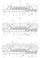
- a step of providing the die bonding material 6 on the substrate 2 having the intra-substrate cavity 30 is performed.
- the die bonding material 6 is provided on the substrate 2 so as to form an endless frame shape in plan view.
- the die bonding material 6 serves as a supporting portion that forms a space portion 7 communicating with the substrate 2 and the image sensor 3 provided on the substrate 2 to one end side of the substrate inner cavity portion 30 .
- a rib resin 46 which is a resin material to be the die bonding material 6, is applied to a predetermined portion of the surface 2a of the substrate 2 by a dispenser or the like in a rectangular frame shape along the outline of the substrate 2 in a plan view.
- the rib resin 46 may be formed by patterning using photolithography or the like.
- a concave portion 47 is formed on the surface 2 a of the substrate 2 , surrounded by the frame-shaped rib resin 46 and having an open top.
- the concave portion 47 is a space inside the die bonding material 6 (rib resin 46) on the surface 2a side of the substrate 2, and is formed by a portion of the surface 2a of the substrate 2 inside the rib resin 46 and four inner side surfaces 46a of the rib resin 46.
- a step of inserting the fluid heat transfer member 20 into the concave portion 47 is performed.
- the heat conductive member 20 is filled in the concave portion 47 by being applied by a dispenser or the like, for example.
- a step of mounting the image sensor 3 on the rib resin 46 is performed.
- the chip of the image sensor 3 is set on the rib resin 46 by a chip mounter or the like and pressed downward against the rib resin 46 and the heat conductive member 20 .
- the rib resin 46 contacts the rear surface 3b of the image sensor 3 over the entire circumference and is slightly crushed by the image sensor 3, and the heat conductive member 20 in the concave portion 47 causes the amount exceeding the volume of the space portion 7 to flow into the substrate cavity portion 30.
- the flow of the heat conductive member 20 into the substrate inner cavity 30 can be promoted.
- the in-space heat conductive member 20A and the in-substrate heat conductive member 20B are present.
- a step of curing the rib resin 46 is performed according to the material of the rib resin 46 and the like.
- a heating step (curing) is performed to harden the rib resin 46 .
- a configuration is obtained in which the space 7 formed by the die bonding material 6 between the substrate 2 and the image sensor 3 is filled with the heat conductive member 20 .
- the step of mounting the image sensor 3 with the heat conductive member 20 in the concave portion 47 corresponds to the step of placing the image sensor 3 on the die bonding material 6 to form the space 7 and filling the space 7 with the heat conductive member 20.
- a step of providing bonding wires 9 electrically connecting the substrate 2 and the image sensor 3 is performed.
- wire bonding is performed for electrically connecting the electrodes formed on the surface 2a of the substrate 2 and the pad electrodes 14 of the image sensor 3 with the bonding wires 9.
- a step of providing a frame 4 on the substrate 2 for supporting the glass 5 provided for the image sensor 3 on the substrate 2 is performed.
- the frame 4 is arranged with respect to the substrate 2 so that the lower surface 4d is positioned at the peripheral edge of the surface 2a of the substrate 2, and is fixed to the substrate 2 with an adhesive such as an epoxy resin adhesive.
- the adhesive is applied to at least one of the frame 4 side and the substrate 2 side along the outer shape of the substrate 2 along the entire circumference.
- the method for manufacturing the solid-state imaging device 1 includes, after the step of filling the space 7 with the heat conductive member 20, the step of providing the frame 4 on the substrate 2 as a step of closing the second opening 32, which is the opening on the other end side of the substrate inner cavity 30.
- a step of providing the glass 5 on the frame 4 is performed.
- the glass 5 is prepared, for example, by cutting a glass plate having a predetermined shape into a rectangular shape by dicing.
- the glass 5 is mounted and fixed on the upper surface 4a of the frame 4 so as to close the opening 4g of the frame 4 from above, with adhesive applied to a predetermined portion of the upper surface 4a of the frame 4. As shown in FIG. 4C, a step of providing the glass 5 on the frame 4 is performed.
- the glass 5 is prepared, for example, by cutting a glass plate having a predetermined shape into a rectangular shape by dicing.
- the glass 5 is mounted and fixed on the upper surface 4a of the frame 4 so as to close the opening 4g of the frame 4 from above, with adhesive applied to a predetermined portion of the upper surface 4a of the frame 4. As shown in FIG.
- the solid-state imaging device 1 as shown in FIGS. 1 and 2 is obtained through the manufacturing process described above.
- the thermal conductivity from the image sensor 3 to the substrate 2 side can be improved, and the cooling efficiency of the image sensor 3 can be improved, so that the stability of the heat dissipation characteristics can be obtained.
- the solid-state imaging device 1 has a configuration in which a space 7 formed on the substrate 2 on the back surface 3b side of the image sensor 3 is filled with a heat conductive member 20 .
- the heat conductive member 20 can improve the heat dissipation of the image sensor 3, and the thermal conductivity from the image sensor 3 to the substrate 2 can be improved. Thereby, the heat dissipation property of the solid-state imaging device 1 can be improved.
- the substrate 2 has an intra-substrate cavity portion 30 communicating with the space portion 7 .
- the heat conductive member 20 it is possible to prevent the heat conductive member 20 from flowing out (leaking) from the outer periphery of the chip of the image sensor 3 to the outside of the space 7 .
- the heat conductive member 20 when the heat conductive member 20 has a relatively low viscosity, the heat conductive member 20 tends to leak from the peripheral edge of the image sensor 3. However, the substrate 2 has the inner cavity 30 communicating with the space 7, so that the leakage of the heat conductive member 20 can be effectively suppressed. As a result, restrictions on the physical properties of the heat transfer member 20 such as the viscosity of the heat transfer member 20 can be relaxed, and the selection of materials that can be used as the heat transfer member 20 can be expanded.
- the heat conductive member 20 can escape into the substrate inner cavity portion 30, so that the space portion 7 can be reliably filled with the heat conductive member 20 without leaking the heat conductive member 20 from the peripheral portion of the image sensor 3. Thereby, the thermal conductivity from the image sensor 3 to the substrate 2 side can be reliably improved.
- the substrate 2 since the substrate 2 has the intra-substrate hollow portion 30 , it becomes easy to adjust the amount of the heat conductive member 20 to be inserted into the concave portion 47 on the substrate 2 in the manufacturing process of the solid-state imaging device 1 . Thereby, the efficiency of the manufacturing process of the solid-state imaging device 1 can be improved.
- the cavity 30 in the substrate can be easily formed.
- the substrate intra-cavity portion 30 has a second opening 32 facing the surface 2 a of the substrate 2 outside the space 7 , and the second opening 32 is provided with a closing portion 40 . According to such a configuration, in the manufacturing process of the solid-state imaging device 1, the state of communication with the outside of the substrate inner cavity portion 30 can be ensured, so that the heat conductive member 20 can be reliably guided into the substrate inner cavity portion 30.
- the closed portion 40 of the second opening 32 of the substrate inner cavity portion 30 serves as the joint portion 16 of the frame 4 with respect to the substrate 2 . According to such a configuration, it is not necessary to provide the closing portion 40 for closing the second opening 32 of the substrate inner cavity portion 30 as a dedicated configuration, so that the configuration and manufacturing process of the solid-state imaging device 1 can be simplified.
- the intra-substrate hollow portion 30 has a portion formed so as to form unevenness in a side cross-sectional view of the substrate 2 .
- foreign matter such as air (bubbles) and dust existing together with the heat conductive member 20 in the substrate inner cavity 30 can be prevented from flowing back to the space 7 side.
- the state of the heat conductive member 20 arranged on the back surface 3b side of the image sensor 3 can be stabilized, and the heat dissipation effect of the heat conductive member 20 can be effectively obtained.
- the method for manufacturing the solid-state imaging device 1 includes a step of using the substrate 2 in which the substrate inner cavity portion 30 having the first opening portion 31 and the second opening portion 32 is formed, filling the space portion 7 with the heat conductive member 20, and then closing the second opening portion 32 of the substrate inner cavity portion 30.
- the substrate internal cavity 30 can be communicated with the outside, so that the heat conductive member 20 can be reliably guided into the substrate internal cavity 30.
- the step of providing the frame 4 on the substrate 2 is a step of closing the second opening 32 of the intra-substrate hollow portion 30 .
- the existing process can be used as the process for closing the second opening 32 of the substrate inner cavity 30, so that the manufacturing process of the solid-state imaging device 1 can be simplified.
- a first modified example is a modified example of the configuration of the substrate inner cavity portion 30 .
- the intra-substrate cavity portion 30 has a passage portion 51 with a relatively narrow passage area and an accommodating portion 52 that communicates with the passage portion 51 and has a larger passage area than the passage portion 51.
- the passage portion 51 is a single passage portion having one end serving as the first opening 31 that communicates with the space portion 7 and the other end serving as the second opening 32 that is closed by the joint portion 16, similar to the substrate inner cavity portion 30 shown in FIG.
- the accommodation portion 52 is a relatively wide enlarged hollow portion provided in the middle portion of the passage portion 51 .
- the substrate inner cavity portion 30 has, as the passage portion 51, a first passage portion 51A, which is a portion closer to the first opening 31 than the accommodation portion 52, and a second passage portion 51B, which is a portion closer to the second opening 32 than the accommodation portion 52.
- the housing portion 52 is formed, for example, as a rectangular parallelepiped space portion.
- the accommodating portion 52 communicates the downstream side of the first passage portion 51A with the side surface 52a on the first opening 31 side, and communicates the upstream side of the second passage portion 51B with the side surface 52b on the second opening 32 side.
- the shape of the accommodating portion 52 is not particularly limited.
- the intra-substrate hollow portion 30 has an enlarged portion 53 that opens toward the surface 2 a of the substrate 2 at the end on the second opening 32 side.
- the expanded portion 53 is formed at the upper end portion of the second flow path portion 34, and is a portion in which the area of the flow path cross section (planar cross section) of the second opening 32 is enlarged with respect to the other flow path portion of the second flow path portion 34.
- the expanded portion 53 is a portion in which the opening area of the second opening portion 32 is expanded with respect to the flow passage area of the second passage portion 51B.
- the expanded portion 53 may be formed, for example, as a diameter-enlarged portion with respect to the passage portion 51, or may be formed as a groove-shaped portion extending in a direction along the surface 2a of the substrate 2 (for example, a direction perpendicular to the paper surface of FIG. 5).
- the intra-substrate cavity portion 30 has a housing portion 52 in an intermediate flow passage portion 35 between the first flow passage portion 33 and the second flow passage portion 34, and an enlarged portion 53 at the upper end of the second flow passage portion 34.
- the substrate inner cavity portion 30 has a channel portion having an uneven shape by alternately and repeatedly arranging vertical channel portions 35c and horizontal channel portions 35d in a portion of the intermediate channel portion 35 closer to the second opening 32 than the housing portion 52.
- the heat conductive member 20 is filled in the substrate inner cavity portion 30 from the first flow path portion 33 communicating with the space portion 7 to the accommodation portion 52 and occupies a range halfway up the expanded portion 53.
- the heat conductive member 20 can be stored in the accommodation portion 52 .
- the heat dissipation effect of the substrate 2 can be improved, and the heat dissipation performance of the solid-state imaging device 1 can be improved.
- the substrate inner cavity portion 30 has the accommodation portion 52, it is possible to effectively suppress foreign matter such as air (bubbles) and dust existing together with the heat conductive member 20 in the substrate inner cavity portion 30 from flowing back to the space portion 7 side.
- the expanding portion 53 can secure a space for receiving the heat conductive member 20 on the surface 2 a side of the substrate 2 . Thereby, it is possible to prevent the heat conductive member 20 reaching the second opening 32 from the space 7 side from flowing out from the surface 2 a of the substrate 2 .
- a second modification is a modification of the configuration of the substrate 2 .
- the substrate 2 has a protrusion 60 provided along the inner side of the die bonding material 6 and protruding from the surface 2a of the substrate 2 .
- the protrusion 60 is located on the inner peripheral side of the die bonding material 6 which has a rectangular frame shape in plan view.
- the projecting portion 60 is provided over the entire circumference along the outer shape of the die bonding material 6 in a plan view, and is endlessly formed to have a rectangular frame shape in a plan view. Therefore, the projection 60 has four side portions 60 a along each side of the rectangular frame-shaped outer shape of the die bonding material 6 .
- the protrusion 60 is provided at a position corresponding to the peripheral region 13 of the image sensor 3 so as to surround the region where the pixel region 12 of the image sensor 3 is formed in plan view.
- the protrusion 60 has a protruding shape in which the cross-sectional shape of the side portion 60a is along a rectangular shape.
- the projecting portion 60 is located inside the die bonding material 6 and intervenes between the front surface 2a of the substrate 2 and the back surface 3b of the image sensor 3, supporting the substrate 2 and the image sensor 3 in a spaced apart state.
- the projection 60 forms a space 7 between the substrate 2 and the image sensor 3 by the inner surface 60b together with the front surface 2a of the substrate 2 and the back surface 3b of the image sensor 3. As shown in FIG.
- the protrusion 60 is fully contacted by the die bonding material 6 on the outer surface 60c. Moreover, the protrusion 60 has an upper surface 60 d that has a frame shape in a plan view and extends along a horizontal plane as a contact surface with the back surface 3 b of the image sensor 3 . The protrusion 60 brings the upper surface 60 d into contact with the rear surface 3 b of the image sensor 3 over the entire surface.
- the protrusion 60 is provided as part of the substrate 2 .
- the projecting portion 60 is formed by stacking a sheet-like member having a frame shape in a plan view and made of a ceramic material on the surface serving as the surface 2a of the substrate 2.
- the protrusion 60 may be a portion formed by performing processing such as cutting or etching on the front surface 2a side of the substrate 2 .
- the protrusion 60 may be partially provided in the circumferential direction with respect to the outer shape of the die bonding material 6 in plan view.
- the protrusion 60 may be a portion provided as two side portions 60a along a pair of side portions 6a facing the frame-shaped die bonding material 6 in plan view.
- the protrusion 60 may be a portion intermittently (partially) provided in the circumferential direction with respect to the inner peripheral side of the frame-shaped die bonding material 6 in plan view.
- the protrusion 60 is not limited to a portion provided as a part of the substrate 2, and may be a portion provided by fixing a separate member to the substrate 2. Specifically, the protrusion 60 may be a portion provided by fixing a frame-shaped member made of ceramics such as glass, or an inorganic material such as metal or silicon to the surface 2a of the substrate 2 with an adhesive or the like. Further, the position where the protrusion 60 is provided on the back side of the image sensor 3 is not particularly limited.
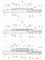
- the rib resin 46 is applied by a dispenser or the like, the rib resin 46 to be the die bonding material 6 is applied so as to entirely cover the outer surface 60c of the protrusion 60.
- a concave portion 67 surrounded by the frame-shaped projecting portion 60 and having an open top is formed on the surface 2 a of the substrate 2 as a space for receiving the heat conductive member 20 .
- the recess 67 is a space inside the projection 60 on the surface 2 a side of the substrate 2 , and is formed by a portion of the surface 2 a of the substrate 2 inside the projection 60 and four inner side surfaces 60 b of the projection 60 .
- a step of mounting the image sensor 3 on the rib resin 46 and the protrusions 60 is performed.
- the chip of the image sensor 3 is set on the rib resin 46 by a chip mounter or the like, and pressed downward against the rib resin 46 , the protrusion 60 and the heat conductive member 20 .
- the rib resin 46 is slightly crushed by the image sensor 3, and the rear surface 3b of the image sensor 3 contacts the upper surface 60d of the projection 60, and part of the heat conductive member 20 in the recess 67 flows into the substrate cavity 30.
- part of the rib resin 46 may enter between the back surface 3 b of the image sensor 3 and the upper surface 60 d of the protrusion 60 .
- a step of curing the rib resin 46 is performed according to the material of the rib resin 46 and the like. As a result, a configuration is obtained in which the space 7 formed by the die bonding material 6 and the protrusion 60 between the substrate 2 and the image sensor 3 is filled with the heat conductive member 20 .
- the step of mounting the image sensor 3 with the heat conductive member 20 in the concave portion 67 corresponds to the step of placing the image sensor 3 on the die bonding material 6 to form the space 7 and filling the space 7 with the heat conductive member 20. Subsequent steps are as described with reference to each diagram of FIG. 4 .
- the protrusion 60 is formed endlessly so as to form a rectangular frame shape in a plan view.
- the projecting portion 60 can be used as a stopper for the image sensor 3 by bringing the projecting portion 60 into contact with the image sensor 3 in the process of mounting the image sensor 3 on the substrate 2. This makes it possible to easily and reliably position the image sensor 3 with respect to the substrate 2 in the vertical direction. As a result, it becomes easy to adjust the amount of the heat-conducting member 20 to be put into the concave portion 67 on the substrate 2 .
- the protrusion 60 as a part of the substrate 2, the protrusion 60 can be easily provided with high accuracy. As a result, leakage of the heat-conducting member 20 can be effectively suppressed, and the manufacturing process of the solid-state imaging device 1 can be made more efficient than when the projecting portion 60 is provided by a member separate from the substrate 2.
- the substrate 2 is formed with a plurality of intra-substrate cavities 30 .
- two substrate internal cavities 30 are formed symmetrically on both left and right sides.
- two substrate internal cavity portions 30 may be formed in the same arrangement as shown in FIG. 8 in a direction orthogonal to the left-right direction in FIG. 8, thereby providing a total of four substrate internal cavity portions 30.
- a plurality of intra-substrate cavities 30 may be formed in the substrate 2 . Further, the intra-substrate cavity 30 may be branched into a plurality of flow paths on the first opening 31 side or the second opening 32 side. In other words, the intra-substrate cavity 30 may have a plurality of at least one of the first openings 31 and the second openings 32 .
- the configuration of the third modified example it is possible to increase the amount of the heat conductive member 20 received by the substrate inner cavity 30 and to disperse the heat conductive member 20 existing in the substrate 2 .
- the substrate 2 can efficiently obtain a heat dissipation effect, and the heat dissipation of the solid-state imaging device 1 can be improved.
- the amount of the heat conductive member 20 received by the substrate inner cavity 30 is increased, it becomes easy to adjust the amount of the heat conductive member 20 to be inserted into the concave portion 67 on the substrate 2 in the manufacturing process of the solid-state imaging device 1 .
- the plurality of intra-substrate cavities 30 are formed symmetrically, for example, in a plane-symmetrical manner or point-symmetrical manner.
- a solid-state imaging device 71 includes a cavity substrate 72 as a substrate according to the present technology. That is, the solid-state imaging device 71 includes a cavity substrate 72, an image sensor 3, and a glass 5, and has a package structure in which the image sensor 3 is mounted in the cavity substrate 72, the glass 5 is mounted on the cavity substrate 72, and the internal space of the cavity substrate 72 is a sealed cavity 78.
- the cavity substrate 72 is a package substrate, and has a rectangular plate-shaped flat plate portion 81 and four wall portions 82 formed along the edges of the flat plate portion 81 to form a rectangular frame shape in plan view.
- the cavity substrate 72 is formed in a box-like shape with a flat plate portion 81 and four wall portions 82 with the upper side being an open side. In other words, the cavity substrate 72 forms a recessed space on the upper side of the flat plate portion 81 with the four walls 82 opening on the upper side.
- the cavity substrate 72 has, in the flat plate portion 81, a front surface 72a which is one plate surface on which the image sensor 3 is mounted, and a back surface 72b which is the other plate surface on the opposite side.
- the image sensor 3 is die-bonded to the surface 72 a of the cavity substrate 72 with the die-bonding material 6 .
- the plate thickness direction of the flat plate portion 81 is the vertical direction in the solid-state imaging device 71, with the front surface 72a side being the upper side and the rear surface 72b side being the lower side.
- the cavity substrate 72 has an upper surface 72c that has a rectangular frame shape in a plan view and extends along a horizontal plane on the upper surface of the four walls 82. As shown in FIG.
- the cavity substrate 72 is a circuit substrate on which a predetermined circuit is formed, and is a multi-layered ceramic substrate in which sheet-shaped members made of ceramic material or the like are laminated, like the substrate 2 of the first embodiment.
- the cavity substrate 72 may be another type of substrate such as an organic substrate using an organic material such as glass epoxy resin, which is a type of fiber-reinforced plastic, as a base material.
- the cavity substrate 72 may be composed of, for example, split elements having the position of the surface 72a in the vertical direction as the upper and lower split positions.
- the cavity substrate 72 has a structure in which a rectangular plate-like portion that forms the flat plate portion 81 and a rectangular cylindrical portion that forms the wall portion 82 are integrally joined.
- the die-bonding material 6 is partially interposed between the front surface 72a of the cavity substrate 72 and the back surface 3b of the image sensor 3, and the flat plate portion 81 and the image sensor 3 are adhered to each other while being separated from each other, thereby forming the airtight space portion 7 between the flat plate portion 81 and the image sensor 3.
- the cavity substrate 72 and the image sensor 3 are electrically connected by a plurality of bonding wires 9.
- the bonding wire 9 has one end connected to an electrode (not shown) formed on the surface 72a of the cavity substrate 72 and the other end connected to the pad electrode 14 of the image sensor 3, thereby electrically connecting these electrodes.
- the electrodes of the cavity substrate 72 to which the bonding wires 9 are connected are electrically connected to a plurality of terminal electrodes 85 formed on the back surface 72b side of the cavity substrate 72 via predetermined wiring portions formed in the cavity substrate 72.
- the glass 5 is fixedly supported on the wall portion 82 of the cavity substrate 72 .
- the glass 5 is fixed on the upper surface 72c of the cavity substrate 72 by a bonding portion 86 formed with an adhesive.
- the bonding portion 86 seals the periphery of the cavity 78 .
- the glass 5 is provided on the light receiving surface side of the image sensor 3 so as to be parallel to the image sensor 3 and spaced apart by a predetermined distance.
- the glass 5 is provided so as to cover the entire upper opening 72d formed by the four walls 82 from above. Therefore, the glass 5 has external dimensions larger than the opening dimensions of the opening 72d.
- the glass 5 has external dimensions slightly smaller than the outer shape of the cavity substrate 72 in plan view, and is positioned within the outer shape of the cavity substrate 72 in plan view.
- the space 7 between the flat plate portion 81 of the cavity substrate 72 and the image sensor 3 is filled with the heat conductive member 20 .
- an intra-substrate cavity portion 30 communicating with the space portion 7 is formed.
- the substrate inner cavity 30 communicates with the space 7 through a first opening 31 on one end side.
- the substrate inner cavity 30 has a second opening 32 on the other end side facing the upper surface 72c of one wall 82 (on the right side in FIG. 9).
- the intra-substrate cavity portion 30 is formed from the flat plate portion 81 to the wall portion 82 in the cavity substrate 72 . That is, the intra-substrate hollow portion 30 has a flat plate portion forming channel portion 91 which is a portion formed in the flat plate portion 81 and a wall portion forming channel portion 92 which is a portion formed in the wall portion 82 .
- the flat plate portion forming channel portion 91 is a channel portion formed mainly in the lateral direction (horizontal direction), and the wall portion forming channel portion 92 is a channel portion formed mainly in the vertical direction (vertical direction).
- the flat plate portion forming channel portion 91 has a vertical channel portion 91a which is a channel portion extending in the vertical direction and whose upper end side is the first opening 31, and a horizontal channel portion 91b forming a right angle with the vertical channel portion 91a.
- the wall-forming channel portion 92 is formed as a vertical channel portion that extends in the vertical direction and has the second opening 32 on the upper end side. The lower end portion of the wall-forming channel portion 92 communicates with the downstream side of the lateral channel portion 91 b of the flat-plate portion-forming channel portion 91 .
- an accommodation portion 52 having a larger channel area than the other channel portions (passage portions) of the wall-forming channel portion 92 is formed in the upper and lower intermediate portions.
- the accommodating portion 52 is a relatively wide enlarged hollow portion provided in the middle portion of the wall-forming channel portion 92 .
- an enlarged portion 53 that is open facing the upper surface 72c of the cavity substrate 72 is formed at the upper end of the wall-forming channel portion 92.
- the expanded portion 53 is a portion obtained by expanding the opening area of the second opening 32 with respect to the flow path area of the other flow path portion of the wall-forming flow path portion 92 .
- the widening portion 53 may be formed, for example, as a diameter-enlarged portion with respect to other portions of the wall-forming channel portion 92, or may be formed as a groove-shaped portion extending in a direction along the upper surface 72c of the cavity substrate 72 (for example, a direction perpendicular to the paper surface of FIG. 9).
- the shape of the substrate inner cavity 30 is not particularly limited.
- a channel portion having an uneven shape in a side sectional view of the cavity substrate 72 may be formed in the flat plate portion forming channel portion 91 .
- a closing portion 40 that closes the other end side of the intra-substrate cavity portion 30 is provided.
- the closing portion 40 is a joint portion 86 of the glass 5 provided for the image sensor 3 and the upper surface 72 c of the cavity substrate 72 .
- the glass 5 serves as a closing member that closes the second opening 32 of the cavity 30 in the substrate from the upper surface 72c side of the cavity substrate 72, and the joining portion 86 for fixing the glass 5 to the cavity substrate 72 serves as the closing portion 40, closing the second opening 32. Therefore, the intra-substrate cavity 30 opens the second opening 32 in the upper surface 72c of the cavity substrate 72 so as to face the area facing the rear surface 5b of the glass 5, and closes the second opening 32 with the joint 86 interposed between the upper surface 72c of the cavity substrate 72 and the rear surface 5b of the glass 5.
- the second opening 32 of the intra-substrate cavity 30 may be closed by a separately provided closing member.
- a step of providing the die bonding material 6 on the cavity substrate 72 having the intra-substrate cavity portion 30 is performed.
- the die bonding material 6 is provided on the cavity substrate 72 so as to form an endless frame shape in plan view.
- the die bonding material 6 serves as a supporting portion that forms a cavity portion 7 that communicates with one end side of the intra-substrate hollow portion 30 together with the cavity substrate 72 and the image sensor 3 provided on the cavity substrate 72 .
- a rib resin 46 which is a resin material to be the die bonding material 6, is applied to a predetermined portion of the surface 72a of the cavity substrate 72 along the outline of the cavity substrate 72 in plan view in a rectangular frame shape. Thereby, recesses 47 are formed on the surface 72 a of the cavity substrate 72 .
- a step of mounting the image sensor 3 on the rib resin 46 is performed.
- the chip of the image sensor 3 is pressed downward against the rib resin 46 and the heat conductive member 20 .
- the heat conductive member 20 that exceeds the volume of the space 7 flows into the substrate inner cavity 30 .
- a step of curing the rib resin 46 is performed to obtain a configuration in which the space 7 formed by the die bonding material 6 between the cavity substrate 72 and the image sensor 3 is filled with the heat conductive member 20 .
- a step of providing bonding wires 9 for electrically connecting the cavity substrate 72 and the image sensor 3 is performed.
- a step of providing the glass 5 provided for the image sensor 3 on the cavity substrate 72 is performed.
- the glass 5 is mounted on the upper surface 72c so as to cover the opening 72d of the cavity substrate 72 from above and is fixed with an adhesive.
- the adhesive is applied to at least one of the cavity substrate 72 side and the glass 5 side along the outer shape of the glass 5 along the entire circumference.
- the method for manufacturing the solid-state imaging device 71 includes, after the step of filling the space 7 with the heat conductive member 20, the step of providing the glass 5 on the cavity substrate 72 as the step of closing the second opening 32, which is the opening on the other end side of the substrate inner cavity 30.
- a solid-state imaging device 71 as shown in FIG. 9 is obtained through the manufacturing process described above.
- the thermal conductivity from the image sensor 3 to the cavity substrate 72 side can be improved, and the cooling efficiency of the image sensor 3 can be improved, so that the stability of the heat dissipation characteristics can be obtained. Further, since the cavity substrate 72 has the intra-substrate hollow portion 30, the same effect as in the case of the first embodiment can be obtained.
- the cavity substrate 72 has the wall portion 82 provided on the upper side of the flat plate portion 81, the portion where the substrate inner cavity portion 30 is formed can be increased.
- the amount of the heat conductive member 20 received by the substrate inner cavity 30 can be increased, so that the heat dissipation of the solid-state imaging device 71 can be improved.
- the amount of the heat conductive member 20 received by the intra-substrate cavity 30 increases, it becomes easy to adjust the amount of the heat conductive member 20 to be inserted into the concave portion 47 on the cavity substrate 72 in the manufacturing process of the solid-state imaging device 71 .
- the intra-substrate hollow portion 30 has the accommodating portion 52 and the expanding portion 53, so that the functions and effects of the accommodating portion 52 and the expanding portion 53 can be obtained as in the case of the first embodiment.
- the cavity substrate 72 is a ceramic substrate having a multi-layered structure in which sheet-like members are laminated, the intra-substrate hollow portion 30 extending from the flat plate portion 81 to the wall portion 82 can be easily formed.
- the closing portion 40 provided for the second opening 32 of the intra-substrate cavity portion 30 serves as the joining portion 86 of the glass 5 to the cavity substrate 72 . According to such a configuration, it is not necessary to provide the closing portion 40 for closing the second opening 32 of the substrate inner cavity portion 30 as a dedicated configuration, so the configuration and manufacturing process of the solid-state imaging device 71 can be simplified.
- the step of providing the glass 5 on the cavity substrate 72 is a step of closing the second opening 32 of the intra-substrate cavity 30 .
- the existing process can be used as the process for closing the second opening 32 of the substrate inner cavity 30, so that the manufacturing process of the solid-state imaging device 71 can be simplified.
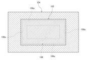
- FIG. 13 is a cross-sectional view taken along line BB of FIG. 12, with a part of the configuration omitted.
- a semiconductor device 101 includes a substrate 102, an IC chip 103 as a semiconductor element provided on the substrate 102, and a sealing resin portion 104 formed around the IC chip 103 on the substrate 102.
- the IC chip 103 is bonded to the substrate 102 with a die bonding material 106 made of an insulating or conductive adhesive or the like. That is, the semiconductor device 101 has a die bonding material 106 that supports the IC chip 103 with respect to the substrate 102 .
- the die bonding material 106 is a supporting portion that forms a space portion 107 together with the substrate 102 and the IC chip 103 .
- the substrate 102 is a plate-like member having a rectangular plate-like outer shape.
- the substrate 102 has a front surface 102a on which the IC chip 103 is mounted, a back surface 102b on the opposite side, and four side surfaces 102c.
- An IC chip 103 is die-bonded to the front surface 102 a of the substrate 102 with a die-bonding material 106 . That is, the die bonding material 106 provided on the surface 102a of the substrate 102 supports the IC chip 103 so as to face the substrate 102 in parallel with the surface 102a.
- the substrate 102 is a circuit board on which a predetermined circuit is formed, and is, for example, a multi-layered ceramic substrate in which sheet-shaped members made of ceramic material or the like are laminated, similar to the substrate 2 of the first embodiment.
- the IC chip 103 is a rectangular plate-shaped semiconductor chip having a predetermined circuit structure.
- the IC chip 103 is, for example, a logic IC such as a CPU (Central Processing Unit) or a memory IC such as a DRAM (Dynamic Random Access Memory).
- a logic IC such as a CPU (Central Processing Unit) or a memory IC such as a DRAM (Dynamic Random Access Memory).
- the die bonding material 106 has the same configuration as the die bonding material 6 according to the first embodiment, and is interposed between the front surface 102a of the substrate 102 and the back surface 103b of the IC chip 103.
- a space 107 which is a closed space, is formed between the substrate 102 and the IC chip 103.
- the die bonding material 106 is endlessly formed along the periphery of the IC chip 103 along the outer shape of the IC chip 103 so as to form a rectangular frame in plan view. Accordingly, the die bonding material 106 has four side portions 106 a along each side of the rectangular outer shape of the IC chip 103 .
- the substrate 102 and the IC chip 103 are electrically connected by a plurality of bonding wires 109.
- the bonding wire 109 has one end connected to an electrode (not shown) formed on the surface 102a of the substrate 102 and the other end connected to an electrode (not shown) formed on the surface 103a of the IC chip 103, thereby electrically connecting these electrodes.
- the electrodes of the substrate 102 to which the bonding wires 109 are connected are electrically connected to a plurality of terminal electrodes 115 formed on the rear surface 102b side of the substrate 102 via predetermined wiring portions formed in the substrate 102.
- the sealing resin portion 104 is a resin portion that covers and seals the die bonding material 106 and the IC chip 103 on the substrate 102 over the entire circumference and from above.
- the sealing resin portion 104 entirely covers the bonding wire 9 and connection portions at both ends thereof.
- the encapsulation resin portion 104 covers the entire outer surface 106c of the die bonding material 106, the portion of the surface 102a of the substrate 102 outside the die bonding material 6, the surface 103a and the four side surfaces 103c of the IC chip 103, and the die bonding material 106, while the bonding wires 9 are entirely buried.
- the sealing resin portion 104 has a rectangular plate-like outer shape that follows the rectangular outer shape of the substrate 102 in plan view, and is formed as a layer portion on the substrate 102 in which the IC chip 103 and the like are embedded.
- the sealing resin portion 104 has a flat upper surface 104a and four side surface portions 104c that are continuous with the side surfaces 102c of the substrate 102 so as to be flush with each other.
- the encapsulating resin portion 104 is formed by curing a resin material around the IC chip 103 on the substrate 102 in a configuration in which the IC chip 103 is mounted on the substrate 102 and these are connected by bonding wires 9 .
- the sealing resin portion 104 is formed into a predetermined shape by injection molding using a molding die, for example.
- the sealing resin portion 104 may be a portion formed by potting using a dispenser, for example.
- the sealing resin portion 104 is formed by applying a resin material that will become the sealing resin portion 104 to a predetermined portion while being discharged from the nozzle of the dispenser, and then curing the resin material.
- the material of the sealing resin portion 104 is, for example, a thermosetting resin containing silicon oxide as a main component or alumina as a filler.
- a thermosetting resin containing silicon oxide as a main component or alumina as a filler for example, thermosetting resins such as phenol-based resins, silicone-based resins, acrylic-based resins, epoxy-based resins, urethane-based resins, silicon resins, and polyetheramide-based resins, thermoplastic resins such as polyamideimide, polypropylene, and liquid crystal polymers, photosensitive resins such as UV-curable resins that are acrylic resins, rubbers, and other known resin materials are used singly or in combination.
- the sealing resin portion 104 has an insulating property.
- the space 107 between the substrate 102 and the IC chip 103 is filled with the heat conductive member 20 .
- an intra-substrate cavity portion 30 communicating with the space portion 107 is formed.
- the substrate inner cavity 30 communicates with the space 107 through a first opening 31 on one end side. Further, the substrate inner cavity portion 30 has a second opening 32 on the other end side outside the space portion 107 so as to face the surface 102 a of the substrate 102 through the second opening 32 . In the example shown in FIG. 12 , the intra-substrate cavity 30 has the second opening 32 positioned at the edge of one side (the right side in FIG. 12 ) of the substrate 102 .
- the intra-substrate cavity portion 30 has a first channel portion 33 and a second channel portion 34 extending in the vertical direction, and an intermediate channel portion 35 extending in the horizontal direction. Further, in the intermediate portion of the intermediate flow path portion 35, a housing portion 52 having a larger flow path area than the other flow path portion (passage portion) of the intermediate flow path portion 35 is formed. A widened portion 53 is formed at the upper end portion of the second flow path portion 34 so as to face the surface 102 a of the substrate 102 .
- a closing portion 40 is provided to close the other end side of the substrate inner cavity portion 30 .
- the closing part 40 is a sealing resin part 104 formed on the substrate 102 .
- the second opening 32 of the intra-substrate cavity 30 may be closed by a separately provided closing member.
- the following steps are performed in the same manner as in the first embodiment. That is, after a rib resin as a die-bonding material 106 is applied onto the surface 102a of the substrate 102 having the intra-substrate cavity 30, the heat conductive member 20 is placed in the recess formed by the rib resin. After that, the IC chip 103 is mounted on the rib resin so as to press against the rib resin and the heat conductive member 20 , so that part of the heat conductive member 20 flows into the substrate inner cavity 30 . Then, wire bonding is performed by disposing bonding wires 109 between the substrate 102 and the IC chip 103 .
- a step of providing a sealing resin portion 104 around the IC chip 103 on the substrate 102 is performed.
- the sealing resin portion 104 is molded using, for example, a mold for molding the molded resin portion.
- a mold for forming the sealing resin portion 104 is, for example, a transfer mold having an upper mold and a lower mold forming a cavity, which is a molding space, together with the upper mold.
- a workpiece for forming the sealing resin portion 104 is set in the mold. The work has the configuration shown in FIG. 14A.
- the mold After the workpiece is set in the mold, the mold is clamped to clamp the workpiece and form a cavity. Thereafter, a molten resin material is injected and filled into the cavity, and the resin material is cured by performing predetermined processing such as heating and cooling on the resin material. Thereby, a resin portion that becomes the sealing resin portion 104 is formed. After that, the clamping of the mold is released, the mold is opened, and the injection-molded work is taken out.
- the workpiece set in the mold may be a chip-shaped workpiece corresponding to the semiconductor device 101, or may be an integrated substrate sheet formed by gathering the substrates 102 and having a plurality of IC chips 103 provided thereon.
- the workpiece set in the mold uses a substrate sheet, the workpiece removed from the mold after the injection molding process is subjected to a dicing process in which predetermined regions corresponding to the semiconductor devices 101 are cut out and separated into individual pieces.
- the sealing resin portion 104 seals the second opening portion 32 of the substrate inner cavity portion 30 that opens at the peripheral portion of the surface 102 a of the substrate 102 .
- the method of manufacturing the semiconductor device 101 according to the present embodiment includes, after the step of filling the space portion 107 with the heat conductive member 20, the step of providing the sealing resin portion 104 on the substrate 2 as a step of closing the second opening portion 32, which is the opening portion on the other end side of the substrate inner cavity portion 30.
- the semiconductor device 101 as shown in FIGS. 12 and 13 is obtained through the manufacturing process described above.
- the thermal conductivity from the IC chip 103 to the substrate 102 side can be improved, and the cooling efficiency of the IC chip 103 can be improved, so that the stability of the heat dissipation characteristics can be obtained. Further, since the substrate 102 has the intra-substrate hollow portion 30, it is possible to obtain the same effect as in the case of the first embodiment.
- the closing portion 40 provided for the second opening portion 32 of the substrate inner cavity portion 30 serves as the sealing resin portion 104 provided on the substrate 102 . With such a configuration, it is not necessary to provide the closing portion 40 for closing the second opening 32 of the substrate inner cavity portion 30 as a dedicated configuration, so that the configuration and manufacturing process of the semiconductor device 101 can be simplified.
- the step of providing the sealing resin portion 104 on the substrate 102 is a step of closing the second opening portion 32 of the substrate inner cavity portion 30 .
- the existing process can be used as the process for closing the second opening 32 of the cavity 30 in the substrate, so that the manufacturing process of the semiconductor device 101 can be simplified.
- the semiconductor device according to this embodiment is the light emitting device 131 .
- the light emitting device 131 constitutes a distance measuring device together with an imaging device including an image sensor, for example.
- an imaging device including an image sensor
- light emitted from a light emitting device 131 functioning as a light source is applied to a subject, and light reflected by the subject is received by an imaging device to capture an image of the subject.
- An image signal output from the imaging device is used for measuring (calculating) the distance to the subject in a control unit or the like of the distance measuring device.
- the light emitting device 131 includes a substrate 132, and a VCSEL (Vertical Cavity Surface Emitting LASER) 133 and an LDD (Laser Diode Driver) 143 as semiconductor elements provided on the substrate 132.
- the light emitting device 131 has two semiconductor elements, the VCSEL 133 and the LDD 143 .
- the light emitting device 131 also includes a frame 134 as a support member provided on the substrate 132 and a glass 135 provided on the frame 134 .
- the VCSEL 133 and the LDD 143 are each bonded to the substrate 132 with a die bonding material 136 made of an insulating or conductive adhesive or the like. That is, the light emitting device 131 includes a die bonding material 136 that supports the VCSEL 133 and the LDD 143 with respect to the substrate 132 .
- the die bonding material 136 is a support that forms a space 137 together with the substrate 132 and the VCSEL 133 or LDD 143, respectively.
- the light emitting device 131 has a package structure in which a glass 135 is mounted on a substrate 132 via a frame 134 and a cavity 138 is formed on the substrate 132 .
- a glass 135 is provided above the VCSEL 133 in parallel with the VCSEL 133 , and the frame 134 and the glass 135 together with the substrate 132 form a cavity 138 which is a closed space on the substrate 132 .
- the substrate 132 is a plate-like member having a rectangular plate-like outer shape.
- the substrate 132 has a front surface 132a on which the VCSEL 133 and the LDD 143 are mounted, a back surface 132b on the opposite side, and four side surfaces 132c.
- VCSEL 133 and LDD 143 are die-bonded to surface 132a of substrate 132 by die-bonding material 136, respectively. That is, the die bonding material 136 provided on the surface 132a of the substrate 132 supports the VCSEL 133 and the LDD 143 so as to face the substrate 132 in parallel with the surface 132a.
- the substrate 132 is a circuit substrate on which a predetermined circuit is formed, and is, for example, a multi-layered ceramic substrate in which sheet-shaped members made of ceramic material or the like are laminated in the same manner as the substrate 2 of the first embodiment.
- the VCSEL 133 is, for example, a rectangular plate-shaped element chip, and is a light-emitting element that emits laser light for irradiating a subject.
- the VCSEL 133 has a plurality of light emitting elements having a VCSEL structure arranged in a two-dimensional array, and the upper surface 133a side is the light emitting surface side.
- VCSEL 133 is electrically connected to substrate 132 by a plurality of bonding wires 139 .
- the LDD 143 is, for example, a rectangular plate-shaped element chip, and has a drive circuit for driving the VCSEL 133 .
- the LDD 143 drives the VCSEL 133 using a power supply voltage generated by a power supply circuit (not shown).
- LDD 143 is electrically connected to substrate 132 by a plurality of bonding wires 149 .
- the die bonding material 136 has the same configuration as the die bonding material 6 according to the first embodiment, and is interposed between the front surface 132a of the substrate 132 and the rear surfaces 133b and 143b of the VCSEL 133 and the LDD 143, respectively. A void-like space portion 137 is formed.
- the die-bonding material 136 is endlessly formed around the periphery of each of the VCSEL 133 and the LDD 143 so as to form a rectangular frame shape in a plan view along the outlines of the VCSEL 133 and the LDD 143 in a plan view.
- electrodes to which the bonding wires 139 are connected are electrically connected to a plurality of external terminals 145 formed on the rear surface 132b side of the substrate 132 via predetermined wiring portions formed within the substrate 132.
- the plurality of external terminals 145 constitute a BGA with solder balls.
- a plurality of passive components 144 such as capacitors and resistors are mounted at predetermined positions on the front surface 132a side of the substrate 132 .
- the frame 134 has the same configuration as the frame 4 according to the first embodiment, and is provided on the surface 132a side of the substrate 132 so as to surround the VCSEL 133 and the LDD 143 .
- the frame 134 is a rectangular or square frame-shaped member, and has substantially the same outer dimensions as the outer shape of the substrate 132 in a plan view.
- the frame 134 has a plate-like upper surface portion 134b forming a horizontal upper surface 134a that supports the glass 135, and a peripheral wall portion 134c formed below the upper surface portion 134b and forming a horizontal lower surface 134d.
- the frame 134 has a rectangular opening 134g penetrating vertically above the VCSEL 133 on the top surface 134b.
- the frame 134 is fixed on the surface 132a of the substrate 132 by a bonding portion 146 formed by an adhesive, with the lower surface 134d located on the periphery of the surface 132a of the substrate 132. As shown in FIG.
- the glass 135 is an example of a transparent member, and is provided to the VCSEL 133 via a frame 134.
- the glass 135 has a rectangular plate-like outer shape and has outer dimensions larger than those of the VCSEL 133 .
- the glass 135 is provided on the frame 134 so as to be parallel to the VCSEL 133 at a predetermined interval on the light emitting surface side of the VCSEL 133 .
- the glass 135 is arranged to cover the entire opening 134g of the frame 134 from above, and is fixed to the upper surface 134a of the frame 134 with an adhesive or the like.
- the space 137 between the substrate 132 and the VCSEL 133 and LDD 143 is filled with the heat conductive member 20 .
- an intra-substrate cavity portion 30 communicating with each space portion 137 is formed. That is, in the light-emitting device 131, the substrate inner cavities 30 are provided for the semiconductor elements of the VCSEL 133 and the LDD 143, which are independent of each other.
- the substrate inner cavity 30 provided for each of the VCSEL 133 and the LDD 143 has the same configuration as the substrate inner cavity 30 according to the third embodiment shown in FIG.
- the method of manufacturing the light emitting device 131 includes, after the step of filling the space 137 of each of the VCSEL 133 and the LDD 143 with the heat conductive member 20, the step of providing the frame 134 on the substrate 132 as a step of closing the second opening 32, which is the opening on the other end side of the cavity 30 in the substrate.
- the thermal conductivity from the VCSEL 133 and the LDD 143 to the substrate 132 side can be improved, and the cooling efficiency of the VCSEL 133 and the LDD 143 can be improved, so that the stability of the heat dissipation characteristics can be obtained.
- the substrate 132 has the intra-substrate hollow portion 30, it is possible to obtain the same effect as in the case of the first embodiment.
- the closing portion 40 provided for the second opening 32 of the substrate inner cavity portion 30 serves as the joining portion 146 of the frame 134 to the substrate 132, the configuration and manufacturing process of the light emitting device 131 can be simplified.
- Configuration example of electronic device> An application example of the semiconductor device according to the above embodiment to an electronic device will be described with reference to FIG. 16 .
- a semiconductor device (solid-state imaging device) can be applied to general electronic equipment that uses a solid-state imaging device as an image capturing unit (photoelectric conversion unit), such as camera devices such as digital still cameras and video cameras, mobile terminal devices that have an imaging function, and copiers that use a solid-state imaging device as an image reading unit.
- the solid-state imaging device may be formed as a single chip, or may be in the form of a module having an imaging function in which an imaging unit and a signal processing unit or an optical system are packaged together.
- a camera device 200 as an electronic device includes an optical unit 202, a solid-state imaging device 201, a DSP (Digital Signal Processor) circuit 203 as a camera signal processing circuit, a frame memory 204, a display unit 205, a recording unit 206, an operation unit 207, and a power supply unit 208.
- the DSP circuit 203, frame memory 204, display unit 205, recording unit 206, operation unit 207, and power supply unit 208 are appropriately connected via a connection line 209 such as a bus line.
- the solid-state imaging device 201 is, for example, the solid-state imaging device 1 according to the first embodiment described above.
- the optical unit 202 includes a plurality of lenses, takes in incident light (image light) from a subject, and forms an image on the imaging surface of the solid-state imaging device 201 .
- the solid-state imaging device 201 converts the amount of incident light imaged on the imaging surface by the optical unit 202 into an electric signal for each pixel, and outputs the electric signal as a pixel signal.
- the display unit 205 is, for example, a panel type display device such as a liquid crystal panel or an organic EL (Electro Luminescence) panel, and displays moving images or still images captured by the solid-state imaging device 201 .
- a recording unit 206 records a moving image or still image captured by the solid-state imaging device 201 in a recording medium such as a hard disk or a semiconductor memory.
- the operation unit 207 issues operation commands for various functions of the camera device 200 under the user's operation.
- the power supply unit 208 appropriately supplies various power supplies as operating power supplies for the DSP circuit 203, the frame memory 204, the display unit 205, the recording unit 206, and the operation unit 207 to these supply targets.
- the thermal conductivity from the image sensor 3 to the substrate 2 side can be improved, and the cooling efficiency of the image sensor 3 can be improved, so that the stability of heat dissipation characteristics can be obtained.
- the semiconductor elements are the image sensor 3, the IC chip 103, the VCSEL 133 and the LDD 143, but the semiconductor elements according to the present technology are not limited to these.
- this technique can take the following configurations. (1) a substrate; a semiconductor element provided on the substrate; a heat conductive member having fluidity and filled in a space between the substrate and the semiconductor element; A semiconductor device, wherein the substrate has one or a plurality of intra-substrate cavities that communicate with the space at one end thereof and receive the heat-conducting member. (2) The cavity in the substrate is formed so that the other end side is open facing the surface of the substrate, The semiconductor device according to (1), wherein a closing portion that closes the other end side of the hollow portion in the substrate is provided on the surface side of the substrate.
- the closing portion is a supporting member for supporting a transparent member provided for the semiconductor element on the substrate, or a joining portion of the transparent member to the surface of the substrate.
- a sealing resin portion formed around the semiconductor element on the substrate, The semiconductor device according to (2), wherein the closing portion is the sealing resin portion.
- the intra-substrate hollow portion includes a passage portion having a relatively narrow passage area, and a housing portion communicating with the passage portion and having a larger passage area than the passage portion.
- the cavity in the substrate is formed to have unevenness when viewed in cross section from the side of the substrate.
- the inner-substrate hollow portion has, at an end on the other end side, an enlarged portion that opens toward the surface of the substrate.
- (8) further comprising a supporting portion that supports the semiconductor element with respect to the substrate and forms the space portion together with the substrate and the semiconductor element;
- the substrate has a projecting portion provided along the inner side of the supporting portion and projecting from the surface of the substrate.
- the protrusion is provided as part of the substrate.
- a substrate (10) a substrate; a semiconductor element provided on the substrate; a heat conductive member having fluidity and filled in a space between the substrate and the semiconductor element;
- An electronic device comprising a semiconductor device, wherein the substrate has one or a plurality of substrate internal cavities that communicate with the space at one end thereof and receive the heat conductive member.
- (11) a step of providing, on a substrate having an inner cavity portion of which one end side and the other end side are open facing the front surface side, a die bonding material serving as a supporting portion forming a space communicating with one end side of the inner cavity portion of the substrate together with the substrate and a semiconductor element provided on the substrate so as to form an endless shape in a plan view; a step of inserting a heat conductive member having fluidity into the space inside the die bonding material on the surface side of the substrate; A method of manufacturing a semiconductor device, comprising: placing the semiconductor element on the die bonding material to form the space, and filling the space with the heat conductive member.
- Solid-state imaging device (semiconductor device) 2 substrate 2a surface 3 image sensor (semiconductor element) 4 frame (support member) 5 glass (transparent member) 6 Die bonding material (supporting part) 7 space portion 16 joint portion (closure portion) 20 Thermally conductive member 30 Cavity in substrate 31 First opening 32 Second opening 35 Intermediate flow path 35c Vertical flow path 35d Horizontal flow path 40 Closed part 51 Passage 52 Accommodating part 53 Enlarged part 60 Protruding part 71 Solid-state imaging device 72 Cavity substrate 86 Joining part (Closing part) 101 semiconductor device 102 substrate 103 IC chip (semiconductor element) 104 sealing resin part 106 die bonding material (support part) 107 space portion 131 light emitting device (semiconductor device) 132 substrate 133 VCSEL (semiconductor element) 134 frame (support member) 135 glass (transparent member) 136 die bonding material (supporting part) 137 space part 143 LDD (semiconduct
Landscapes
- Solid State Image Pick-Up Elements (AREA)
Abstract
Description
1.第1実施形態に係る半導体装置の構成例
2.第1実施形態に係る半導体装置の製造方法
3.第1実施形態に係る半導体装置の変形例
4.第2実施形態に係る半導体装置の構成例
5.第2実施形態に係る半導体装置の製造方法
6.第3実施形態に係る半導体装置の構成例
7.第3実施形態に係る半導体装置の製造方法
8.第4実施形態に係る半導体装置の構成例
9.電子機器の構成例
本技術の第1実施形態に係る半導体装置の構成例について、図1および図2を参照して説明する。本実施形態では、半導体装置として、半導体素子の一例である固体撮像素子を含む固体撮像装置を例にとって説明する。なお、図1における上下方向を固体撮像装置1における上下方向とする。また、図2は、図1における一部の構成を省略したA-A位置の断面図である。
本技術の第1実施形態に係る固体撮像装置1の製造方法の一例について、図3および図4を参照して説明する。
第1実施形態に係る固体撮像装置1の変形例について説明する。
第1の変形例は、基板内空洞部30の構成についての変形例である。図5に示すように、第1の変形例では、基板内空洞部30は、流路面積が比較的狭い通路部51と、通路部51に連通するとともに通路部51に対して流路面積が広い収容部52とを有する。
第2の変形例は、基板2の構成についての変形例である。図6に示すように、第2の変形例では、基板2は、ダイボンド材6の内側に沿うように設けられ基板2の表面2aから突出した突部60を有する。
図8に示すように、第3の変形例において、基板2には、複数の基板内空洞部30が形成されている。図8に示す例では、左右両側に対称的に2つの基板内空洞部30が形成されている。また、平面視で図8における左右方向に直交する方向について、図8に示す配置と同様の配置で2つの基板内空洞部30を形成することで、合計で4つの基板内空洞部30を有する構成であってもよい。
本技術の第2実施形態に係る固体撮像装置71の構成例について、図9を参照して説明する。以下に説明する各実施形態では、第1実施形態と共通のまたは対応する構成については同一の名称または同一の符号を付し、重複する内容についての説明を適宜省略する。
本技術の第2実施形態に係る固体撮像装置71の製造方法の一例について、図10および図11を参照して説明する。
本技術の第3実施形態に係る半導体装置101の構成例について、図12および図13を参照して説明する。なお、図13は、図12における一部の構成を省略したB-B位置の断面図である。
本技術の第3実施形態に係る半導体装置101の製造方法の一例について、図14を参照して説明する。
本技術の第4実施形態に係る半導体装置の構成例について、図15を参照して説明する。本実施形態に係る半導体装置は、発光装置131である。
上述した実施形態に係る半導体装置の電子機器への適用例について、図16を用いて説明する。
(1)
基板と、
前記基板上に設けられた半導体素子と、
流動性を有し前記基板と前記半導体素子との間の空間部に充填された伝熱性部材と、を備え、
前記基板には、一端側を前記空間部に連通させて前記伝熱性部材を受け入れる一または複数の基板内空洞部が形成されている
半導体装置。
(2)
前記基板内空洞部は、他端側を前記基板の表面に臨んで開口させるように形成されており、
前記基板の表面側には、前記基板内空洞部の他端側を塞ぐ閉塞部が設けられている
前記(1)に記載の半導体装置。
(3)
前記閉塞部は、前記半導体素子に対して設けられる透明部材を前記基板上に支持するための支持部材または前記透明部材の、前記基板の表面に対する接合部である
前記(2)に記載の半導体装置。
(4)
前記基板上における前記半導体素子の周囲に形成された封止樹脂部を備え、
前記閉塞部は、前記封止樹脂部である
前記(2)に記載の半導体装置。
(5)
前記基板内空洞部は、流路面積が比較的狭い通路部と、前記通路部に連通するとともに前記通路部に対して流路面積が広い収容部と、を有する
前記(1)~(4)のいずれか1つに記載の半導体装置。
(6)
前記基板内空洞部は、前記基板の側面断面視で凹凸をなすように形成されている
前記(1)~(5)のいずれか1つに記載の半導体装置。
(7)
前記基板内空洞部は、他端側の端部に、前記基板の表面に臨んで開口した拡開部を有する
前記(1)~(6)のいずれか1つに記載の半導体装置。
(8)
前記基板に対して前記半導体素子を支持し、前記基板および前記半導体素子とともに前記空間部を形成する支持部をさらに備え、
前記基板は、前記支持部の内側に沿うように設けられ前記基板の表面から突出した突部を有する
前記(1)~(7)のいずれか1つに記載の半導体装置。
(9)
前記突部は、前記基板の一部として設けられている
前記(8)に記載の半導体装置。
(10)
基板と、
前記基板上に設けられた半導体素子と、
流動性を有し前記基板と前記半導体素子との間の空間部に充填された伝熱性部材と、を備え、
前記基板には、一端側を前記空間部に連通させて前記伝熱性部材を受け入れる一または複数の基板内空洞部が形成されている
半導体装置を備えた
電子機器。
(11)
一端側および他端側を表面側に臨んで開口させた基板内空洞部を有する基板上に、前記基板および前記基板上に設けられる半導体素子とともに前記基板内空洞部の一端側に連通する空間部を形成する支持部となるダイボンド材を、平面視で無端状の形状をなすように設ける工程と、
前記基板の表面側における前記ダイボンド材の内側の空間に、流動性を有する伝熱性部材を入れる工程と、
前記ダイボンド材の上に前記半導体素子を載せて前記空間部を形成するとともに、前記空間部内に前記伝熱性部材を充填させる工程と、を含む
半導体装置の製造方法。
(12)
前記伝熱性部材を充填させる工程の後に、前記基板内空洞部の他端側の開口部を塞ぐ工程を有する
前記(11)に記載の半導体装置の製造方法。
(13)
前記他端側の開口部を塞ぐ工程は、前記基板上に、前記半導体素子に対して設けられる透明部材または前記透明部材を前記基板上に支持するための支持部材を設ける工程である
前記(12)に記載の半導体装置の製造方法。
(14)
前記他端側の開口部を塞ぐ工程は、前記基板上における前記半導体素子の周囲に封止樹脂部を設ける工程である
前記(12)に記載の半導体装置の製造方法。
2 基板
2a 表面
3 イメージセンサ(半導体素子)
4 フレーム(支持部材)
5 ガラス(透明部材)
6 ダイボンド材(支持部)
7 空間部
16 接合部(閉塞部)
20 伝熱性部材
30 基板内空洞部
31 第1開口部
32 第2開口部
35 中間流路部
35c 縦流路部
35d 横流路部
40 閉塞部
51 通路部
52 収容部
53 拡開部
60 突部
71 固体撮像装置
72 キャビティ基板
86 接合部(閉塞部)
101 半導体装置
102 基板
103 ICチップ(半導体素子)
104 封止樹脂部
106 ダイボンド材(支持部)
107 空間部
131 発光装置(半導体装置)
132 基板
133 VCSEL(半導体素子)
134 フレーム(支持部材)
135 ガラス(透明部材)
136 ダイボンド材(支持部)
137 空間部
143 LDD(半導体素子)
200 カメラ装置(電子機器)
201 固体撮像装置(半導体装置)
Claims (14)
- 基板と、
前記基板上に設けられた半導体素子と、
流動性を有し前記基板と前記半導体素子との間の空間部に充填された伝熱性部材と、を備え、
前記基板には、一端側を前記空間部に連通させて前記伝熱性部材を受け入れる一または複数の基板内空洞部が形成されている
半導体装置。 - 前記基板内空洞部は、他端側を前記基板の表面に臨んで開口させるように形成されており、
前記基板の表面側には、前記基板内空洞部の他端側を塞ぐ閉塞部が設けられている
請求項1に記載の半導体装置。 - 前記閉塞部は、前記半導体素子に対して設けられる透明部材を前記基板上に支持するための支持部材または前記透明部材の、前記基板の表面に対する接合部である
請求項2に記載の半導体装置。 - 前記基板上における前記半導体素子の周囲に形成された封止樹脂部を備え、
前記閉塞部は、前記封止樹脂部である
請求項2に記載の半導体装置。 - 前記基板内空洞部は、流路面積が比較的狭い通路部と、前記通路部に連通するとともに前記通路部に対して流路面積が広い収容部と、を有する
請求項1に記載の半導体装置。 - 前記基板内空洞部は、前記基板の側面断面視で凹凸をなすように形成されている
請求項1に記載の半導体装置。 - 前記基板内空洞部は、他端側の端部に、前記基板の表面に臨んで開口した拡開部を有する
請求項1に記載の半導体装置。 - 前記基板に対して前記半導体素子を支持し、前記基板および前記半導体素子とともに前記空間部を形成する支持部をさらに備え、
前記基板は、前記支持部の内側に沿うように設けられ前記基板の表面から突出した突部を有する
請求項1に記載の半導体装置。 - 前記突部は、前記基板の一部として設けられている
請求項8に記載の半導体装置。 - 基板と、
前記基板上に設けられた半導体素子と、
流動性を有し前記基板と前記半導体素子との間の空間部に充填された伝熱性部材と、を備え、
前記基板には、一端側を前記空間部に連通させて前記伝熱性部材を受け入れる一または複数の基板内空洞部が形成されている
半導体装置を備えた
電子機器。 - 一端側および他端側を表面側に臨んで開口させた基板内空洞部を有する基板上に、前記基板および前記基板上に設けられる半導体素子とともに前記基板内空洞部の一端側に連通する空間部を形成する支持部となるダイボンド材を、平面視で無端状の形状をなすように設ける工程と、
前記基板の表面側における前記ダイボンド材の内側の空間に、流動性を有する伝熱性部材を入れる工程と、
前記ダイボンド材の上に前記半導体素子を載せて前記空間部を形成するとともに、前記空間部内に前記伝熱性部材を充填させる工程と、を含む
半導体装置の製造方法。 - 前記伝熱性部材を充填させる工程の後に、前記基板内空洞部の他端側の開口部を塞ぐ工程を有する
請求項11に記載の半導体装置の製造方法。 - 前記他端側の開口部を塞ぐ工程は、前記基板上に、前記半導体素子に対して設けられる透明部材または前記透明部材を前記基板上に支持するための支持部材を設ける工程である
請求項12に記載の半導体装置の製造方法。 - 前記他端側の開口部を塞ぐ工程は、前記基板上における前記半導体素子の周囲に封止樹脂部を設ける工程である
請求項12に記載の半導体装置の製造方法。
Priority Applications (2)
| Application Number | Priority Date | Filing Date | Title |
|---|---|---|---|
| JP2023575181A JPWO2023140100A1 (ja) | 2022-01-21 | 2022-12-28 | |
| US18/727,754 US20250113634A1 (en) | 2022-01-21 | 2022-12-28 | Semiconductor device, electronic device, and method for manufacturing semiconductor device |
Applications Claiming Priority (2)
| Application Number | Priority Date | Filing Date | Title |
|---|---|---|---|
| JP2022008073 | 2022-01-21 | ||
| JP2022-008073 | 2022-01-21 |
Publications (1)
| Publication Number | Publication Date |
|---|---|
| WO2023140100A1 true WO2023140100A1 (ja) | 2023-07-27 |
Family
ID=87348662
Family Applications (1)
| Application Number | Title | Priority Date | Filing Date |
|---|---|---|---|
| PCT/JP2022/048692 Ceased WO2023140100A1 (ja) | 2022-01-21 | 2022-12-28 | 半導体装置、電子機器および半導体装置の製造方法 |
Country Status (3)
| Country | Link |
|---|---|
| US (1) | US20250113634A1 (ja) |
| JP (1) | JPWO2023140100A1 (ja) |
| WO (1) | WO2023140100A1 (ja) |
Cited By (1)
| Publication number | Priority date | Publication date | Assignee | Title |
|---|---|---|---|---|
| WO2025063157A1 (ja) * | 2023-09-20 | 2025-03-27 | ソニーセミコンダクタソリューションズ株式会社 | 光検出モジュール |
Citations (9)
| Publication number | Priority date | Publication date | Assignee | Title |
|---|---|---|---|---|
| JPH04359496A (ja) * | 1991-06-05 | 1992-12-11 | Oki Electric Ind Co Ltd | 電子部品搭載方法 |
| JP2007299630A (ja) * | 2006-04-28 | 2007-11-15 | Matsushita Electric Works Ltd | 接点開閉装置 |
| US20080150154A1 (en) * | 2006-12-21 | 2008-06-26 | Qimonda Ag | Method for fabricating a circuit |
| JP2008172092A (ja) * | 2007-01-12 | 2008-07-24 | Nikon Corp | 半導体装置 |
| CN201956388U (zh) * | 2010-08-20 | 2011-08-31 | 符建 | 一种基于液态金属基底的软性连接的led装置 |
| JP2012191002A (ja) * | 2011-03-10 | 2012-10-04 | Panasonic Corp | 半導体装置 |
| WO2015102046A1 (ja) * | 2014-01-06 | 2015-07-09 | 三菱電機株式会社 | 半導体装置 |
| JP2019125643A (ja) * | 2018-01-15 | 2019-07-25 | ソニーセミコンダクタソリューションズ株式会社 | 半導体素子、実装基板、半導体装置および半導体装置の製造方法 |
| US20200350228A1 (en) * | 2019-05-01 | 2020-11-05 | Yuci Shen | Heat sink aspect of heat dissipating lid and reservoir structure flip chip package for liquid thermal interfacing materials |
-
2022
- 2022-12-28 JP JP2023575181A patent/JPWO2023140100A1/ja active Pending
- 2022-12-28 WO PCT/JP2022/048692 patent/WO2023140100A1/ja not_active Ceased
- 2022-12-28 US US18/727,754 patent/US20250113634A1/en active Pending
Patent Citations (9)
| Publication number | Priority date | Publication date | Assignee | Title |
|---|---|---|---|---|
| JPH04359496A (ja) * | 1991-06-05 | 1992-12-11 | Oki Electric Ind Co Ltd | 電子部品搭載方法 |
| JP2007299630A (ja) * | 2006-04-28 | 2007-11-15 | Matsushita Electric Works Ltd | 接点開閉装置 |
| US20080150154A1 (en) * | 2006-12-21 | 2008-06-26 | Qimonda Ag | Method for fabricating a circuit |
| JP2008172092A (ja) * | 2007-01-12 | 2008-07-24 | Nikon Corp | 半導体装置 |
| CN201956388U (zh) * | 2010-08-20 | 2011-08-31 | 符建 | 一种基于液态金属基底的软性连接的led装置 |
| JP2012191002A (ja) * | 2011-03-10 | 2012-10-04 | Panasonic Corp | 半導体装置 |
| WO2015102046A1 (ja) * | 2014-01-06 | 2015-07-09 | 三菱電機株式会社 | 半導体装置 |
| JP2019125643A (ja) * | 2018-01-15 | 2019-07-25 | ソニーセミコンダクタソリューションズ株式会社 | 半導体素子、実装基板、半導体装置および半導体装置の製造方法 |
| US20200350228A1 (en) * | 2019-05-01 | 2020-11-05 | Yuci Shen | Heat sink aspect of heat dissipating lid and reservoir structure flip chip package for liquid thermal interfacing materials |
Cited By (1)
| Publication number | Priority date | Publication date | Assignee | Title |
|---|---|---|---|---|
| WO2025063157A1 (ja) * | 2023-09-20 | 2025-03-27 | ソニーセミコンダクタソリューションズ株式会社 | 光検出モジュール |
Also Published As
| Publication number | Publication date |
|---|---|
| US20250113634A1 (en) | 2025-04-03 |
| JPWO2023140100A1 (ja) | 2023-07-27 |
Similar Documents
| Publication | Publication Date | Title |
|---|---|---|
| KR100652375B1 (ko) | 와이어 본딩 패키지를 포함하는 이미지 센서 모듈 구조물및 그 제조방법 | |
| KR100604190B1 (ko) | 고체촬상장치, 반도체 웨이퍼, 광학장치용 모듈,고체촬상장치의 제조방법, 및 광학장치용 모듈의 제조방법 | |
| US8508034B2 (en) | Electronic devices | |
| KR101115181B1 (ko) | 광학적으로 민감한 디바이스들에 대한 렌즈 정렬 방법 및 장치, 및 그를 구현하는 시스템들 | |
| US7593636B2 (en) | Pin referenced image sensor to reduce tilt in a camera module | |
| US9155212B2 (en) | Electronic component, mounting member, electronic apparatus, and their manufacturing methods | |
| JP2004301938A (ja) | 光学装置用モジュール及び光学装置用モジュールの製造方法 | |
| US20140008778A1 (en) | Photonic semiconductor devices in llc assembly with controlled molding boundary and method for forming same | |
| US12317619B2 (en) | Solid-state imaging device and electronic device | |
| CN105590926B (zh) | 电子组件、电子模块、其制造方法以及电子装置 | |
| US20250160012A1 (en) | Semiconductor device, electronic device, and manufacturing method for semiconductor device | |
| CN101299432A (zh) | 光学器件及其制造方法 | |
| WO2023140100A1 (ja) | 半導体装置、電子機器および半導体装置の製造方法 | |
| CN112820749A (zh) | 芯片封装结构、方法和电子设备 | |
| JP2026009410A (ja) | 半導体装置および電子機器 | |
| WO2023032260A1 (ja) | 半導体装置および電子機器 | |
| WO2024053466A1 (ja) | 半導体装置および電子機器 | |
| JP2007317719A (ja) | 撮像装置及びその製造方法 | |
| CN112151560A (zh) | 图像传感器封装件和相关方法 | |
| CN117059677A (zh) | 影像感测模组、显示模组及电子设备 | |
| US20090179290A1 (en) | Encapsulated imager packaging | |
| US20250006755A1 (en) | Semiconductor device and electronic equipment | |
| WO2024225110A1 (ja) | 半導体装置および電子機器 | |
| JP2004282227A (ja) | 光モジュール及びその製造方法並びに電子機器 | |
| KR20230144698A (ko) | 이미지 센서 패키지 |
Legal Events
| Date | Code | Title | Description |
|---|---|---|---|
| 121 | Ep: the epo has been informed by wipo that ep was designated in this application |
Ref document number: 22922250 Country of ref document: EP Kind code of ref document: A1 |
|
| ENP | Entry into the national phase |
Ref document number: 2023575181 Country of ref document: JP Kind code of ref document: A |
|
| WWE | Wipo information: entry into national phase |
Ref document number: 18727754 Country of ref document: US |
|
| NENP | Non-entry into the national phase |
Ref country code: DE |
|
| 122 | Ep: pct application non-entry in european phase |
Ref document number: 22922250 Country of ref document: EP Kind code of ref document: A1 |
|
| WWP | Wipo information: published in national office |
Ref document number: 18727754 Country of ref document: US |