WO2023140001A1 - 配線基板 - Google Patents
配線基板 Download PDFInfo
- Publication number
- WO2023140001A1 WO2023140001A1 PCT/JP2022/046668 JP2022046668W WO2023140001A1 WO 2023140001 A1 WO2023140001 A1 WO 2023140001A1 JP 2022046668 W JP2022046668 W JP 2022046668W WO 2023140001 A1 WO2023140001 A1 WO 2023140001A1
- Authority
- WO
- WIPO (PCT)
- Prior art keywords
- wiring
- insulating layer
- wiring board
- layer
- groove
- Prior art date
- Legal status (The legal status is an assumption and is not a legal conclusion. Google has not performed a legal analysis and makes no representation as to the accuracy of the status listed.)
- Ceased
Links
Images














Classifications
-
- H—ELECTRICITY
- H05—ELECTRIC TECHNIQUES NOT OTHERWISE PROVIDED FOR
- H05K—PRINTED CIRCUITS; CASINGS OR CONSTRUCTIONAL DETAILS OF ELECTRIC APPARATUS; MANUFACTURE OF ASSEMBLAGES OF ELECTRICAL COMPONENTS
- H05K1/00—Printed circuits
- H05K1/02—Details
- H05K1/0274—Optical details, e.g. printed circuits comprising integral optical means
-
- H—ELECTRICITY
- H05—ELECTRIC TECHNIQUES NOT OTHERWISE PROVIDED FOR
- H05K—PRINTED CIRCUITS; CASINGS OR CONSTRUCTIONAL DETAILS OF ELECTRIC APPARATUS; MANUFACTURE OF ASSEMBLAGES OF ELECTRICAL COMPONENTS
- H05K1/00—Printed circuits
- H05K1/18—Printed circuits structurally associated with non-printed electric components
- H05K1/181—Printed circuits structurally associated with non-printed electric components associated with surface mounted components
-
- H—ELECTRICITY
- H05—ELECTRIC TECHNIQUES NOT OTHERWISE PROVIDED FOR
- H05K—PRINTED CIRCUITS; CASINGS OR CONSTRUCTIONAL DETAILS OF ELECTRIC APPARATUS; MANUFACTURE OF ASSEMBLAGES OF ELECTRICAL COMPONENTS
- H05K3/00—Apparatus or processes for manufacturing printed circuits
- H05K3/46—Manufacturing multilayer circuits
- H05K3/4644—Manufacturing multilayer circuits by building the multilayer layer by layer, i.e. build-up multilayer circuits
- H05K3/465—Manufacturing multilayer circuits by building the multilayer layer by layer, i.e. build-up multilayer circuits by applying an insulating layer having channels for the next circuit layer
-
- H—ELECTRICITY
- H10—SEMICONDUCTOR DEVICES; ELECTRIC SOLID-STATE DEVICES NOT OTHERWISE PROVIDED FOR
- H10H—INORGANIC LIGHT-EMITTING SEMICONDUCTOR DEVICES HAVING POTENTIAL BARRIERS
- H10H29/00—Integrated devices, or assemblies of multiple devices, comprising at least one light-emitting semiconductor element covered by group H10H20/00
- H10H29/30—Active-matrix LED displays
- H10H29/49—Interconnections, e.g. wiring lines or terminals
-
- H—ELECTRICITY
- H05—ELECTRIC TECHNIQUES NOT OTHERWISE PROVIDED FOR
- H05K—PRINTED CIRCUITS; CASINGS OR CONSTRUCTIONAL DETAILS OF ELECTRIC APPARATUS; MANUFACTURE OF ASSEMBLAGES OF ELECTRICAL COMPONENTS
- H05K1/00—Printed circuits
- H05K1/02—Details
- H05K1/0286—Programmable, customizable or modifiable circuits
- H05K1/0287—Programmable, customizable or modifiable circuits having an universal lay-out, e.g. pad or land grid patterns or mesh patterns
- H05K1/0289—Programmable, customizable or modifiable circuits having an universal lay-out, e.g. pad or land grid patterns or mesh patterns having a matrix lay-out, i.e. having selectively interconnectable sets of X-conductors and Y-conductors in different planes
-
- H—ELECTRICITY
- H05—ELECTRIC TECHNIQUES NOT OTHERWISE PROVIDED FOR
- H05K—PRINTED CIRCUITS; CASINGS OR CONSTRUCTIONAL DETAILS OF ELECTRIC APPARATUS; MANUFACTURE OF ASSEMBLAGES OF ELECTRICAL COMPONENTS
- H05K2201/00—Indexing scheme relating to printed circuits covered by H05K1/00
- H05K2201/01—Dielectrics
- H05K2201/0104—Properties and characteristics in general
- H05K2201/0108—Transparent
-
- H—ELECTRICITY
- H05—ELECTRIC TECHNIQUES NOT OTHERWISE PROVIDED FOR
- H05K—PRINTED CIRCUITS; CASINGS OR CONSTRUCTIONAL DETAILS OF ELECTRIC APPARATUS; MANUFACTURE OF ASSEMBLAGES OF ELECTRICAL COMPONENTS
- H05K2201/00—Indexing scheme relating to printed circuits covered by H05K1/00
- H05K2201/10—Details of components or other objects attached to or integrated in a printed circuit board
- H05K2201/10007—Types of components
- H05K2201/10106—Light emitting diode [LED]
-
- H—ELECTRICITY
- H05—ELECTRIC TECHNIQUES NOT OTHERWISE PROVIDED FOR
- H05K—PRINTED CIRCUITS; CASINGS OR CONSTRUCTIONAL DETAILS OF ELECTRIC APPARATUS; MANUFACTURE OF ASSEMBLAGES OF ELECTRICAL COMPONENTS
- H05K2203/00—Indexing scheme relating to apparatus or processes for manufacturing printed circuits covered by H05K3/00
- H05K2203/01—Tools for processing; Objects used during processing
- H05K2203/0104—Tools for processing; Objects used during processing for patterning or coating
- H05K2203/0108—Male die used for patterning, punching or transferring
-
- H—ELECTRICITY
- H05—ELECTRIC TECHNIQUES NOT OTHERWISE PROVIDED FOR
- H05K—PRINTED CIRCUITS; CASINGS OR CONSTRUCTIONAL DETAILS OF ELECTRIC APPARATUS; MANUFACTURE OF ASSEMBLAGES OF ELECTRICAL COMPONENTS
- H05K3/00—Apparatus or processes for manufacturing printed circuits
- H05K3/0011—Working of insulating substrates or insulating layers
- H05K3/0014—Shaping of the substrate, e.g. by moulding
-
- H—ELECTRICITY
- H05—ELECTRIC TECHNIQUES NOT OTHERWISE PROVIDED FOR
- H05K—PRINTED CIRCUITS; CASINGS OR CONSTRUCTIONAL DETAILS OF ELECTRIC APPARATUS; MANUFACTURE OF ASSEMBLAGES OF ELECTRICAL COMPONENTS
- H05K3/00—Apparatus or processes for manufacturing printed circuits
- H05K3/10—Apparatus or processes for manufacturing printed circuits in which conductive material is applied to the insulating support in such a manner as to form the desired conductive pattern
- H05K3/107—Apparatus or processes for manufacturing printed circuits in which conductive material is applied to the insulating support in such a manner as to form the desired conductive pattern by filling grooves in the support with conductive material
Definitions
- the present disclosure relates to a wiring board having wiring, and more particularly to a wiring board in which wiring is embedded in grooves of an insulating layer formed on a film.
- Wiring boards with wiring are used in electronic devices.
- the wiring board is used as a mounting board on which electronic components such as circuit elements or light emitting elements are mounted, used as a touch sensor board provided with sensor electrodes, or used as a connection board for electrically connecting electrical members.
- a display device in which a plurality of light-emitting elements such as LEDs are arranged in a matrix on the wiring substrate.
- a touch panel in which sensor electrodes are arranged in a matrix on a wiring substrate is known (for example, Patent Document 1).
- the imprint method is a technique of forming grooves in an insulating layer by transferring the uneven structure to a resin material using a mold member (mold) having a fine uneven structure, and forming fine wiring in the grooves.
- the insulating layer in which the wiring is embedded in the wiring substrate consists only of a single layer. Therefore, if the wiring is formed in the insulating layer so as to form a pattern for driving the light emitting elements arranged in a matrix, there will be an area where a large number of wiring must be formed between the adjacent light emitting elements. Therefore, when the wiring board is viewed from above, the wiring occupies a large proportion. As a result, the pitch of the light-emitting elements cannot be reduced, and high-definition images cannot be displayed.
- the present disclosure has been made to solve such problems, and an object thereof is to provide a wiring board that can reduce the ratio of wiring when viewed from the top.
- one aspect of the wiring board according to the present disclosure includes a resin film, a first insulating layer positioned above the film and having a first groove, a conductive first wiring formed in the first groove, a second insulating layer positioned above the first insulating layer and having a second groove and an opening positioned above the first wiring, a conductive second wiring formed in the second groove and the opening, wherein the first groove has a first bottom surface and a first side surface continuously connected to the first bottom surface, the first insulating layer is made of the same material on the first bottom surface and the first side surface, the second groove portion has a second bottom surface and a second side surface continuously connected to the second bottom surface, the second insulating layer is made of the same material on the second bottom surface, the second side surface, and the side surface of the opening, and the top surface of the first wiring and the lower surface of the second wiring formed in the opening.
- FIG. 1 is a perspective view of a wiring board according to Embodiment 1.
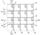
- FIG. FIG. 2 is a top view of the wiring board according to Embodiment 1.
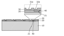
- FIG. 4A is a diagram for explaining a step of forming a first insulating layer in the wiring board manufacturing method according to Embodiment 1.
- FIG. 4B is a diagram for explaining the step of forming the first groove in the first insulating layer in the method of manufacturing the wiring board according to Embodiment 1.
- FIG. 1 is a perspective view of a wiring board according to Embodiment 1.
- FIG. FIG. 2 is a top view of the wiring board according to Embodiment 1.
- FIG. 3A is a cross-sectional view of the wiring board according to
- FIG. 4C is a diagram for explaining the step of forming the first wiring in the method of manufacturing the wiring board according to Embodiment 1.
- FIG. 4D is a diagram for explaining the step of forming the second insulating layer in the method for manufacturing the wiring board according to Embodiment 1.
- FIG. 4E is a diagram for explaining the step of forming the first recess and the second recess in the second insulating layer in the method of manufacturing the wiring board according to Embodiment 1.
- FIG. 4F is a diagram for explaining the step of forming the first groove and the opening in the second insulating layer in the method of manufacturing the wiring board according to Embodiment 1.
- FIG. 4G is a diagram for explaining a step of forming the second wiring in the method of manufacturing the wiring board according to Embodiment 1.
- FIG. 4H is a diagram for explaining a step of mounting a circuit element in the wiring board manufacturing method according to the first embodiment.
- FIG. 5A and 5B are diagrams for explaining a step of forming the first recess and the second recess in the second insulating layer in the wiring board manufacturing method according to the modification of the first embodiment.
- 6 is a perspective view of a wiring board of Comparative Example 1.
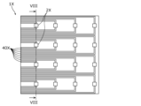
- FIG. 7 is a top view of the wiring board of Comparative Example 1.
- FIG. FIG. 8 is a cross-sectional view of the wiring board of Comparative Example 1 along line VIII-VIII of FIG. 9 is a cross-sectional view of a wiring board according to a modification of Embodiment 1.
- FIG. 10 is a diagram for explaining a method of forming a black layer on the first wiring.
- FIG. 11 is a cross-sectional view of a wiring board according to Embodiment 2.
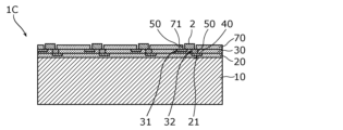
- FIG. 12 is a cross-sectional view of a wiring board according to Embodiment 3.
- FIG. 13 is a cross-sectional view of a wiring board according to Modification 1 of Embodiment 3.
- FIG. 14 is a cross-sectional view of a wiring board according to Modification 2 of Embodiment 3.
- FIG. 15 is a cross-sectional view of a wiring board according to Modification 3 of Embodiment 3.
- FIG. 16 is a cross-sectional view of a wiring board according to Embodiment 4.
- FIG. 17 is a top view of a wiring board according to Embodiment 5.
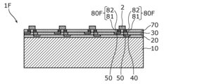
- FIG. FIG. 18 is a cross-sectional view of the wiring board according to the fifth embodiment along line XVIII-XVIII in FIG. 19 is a top view of a wiring board according to Modification 1 of Embodiment 5.
- FIG. FIG. 20 is a cross-sectional view of a wiring board according to Modification 1 of Embodiment 5 taken along line XX-XX of FIG.
- FIG. 21 is a top view of a wiring board according to Embodiment 6.
- FIG. 22 is a top view of a wiring board of Comparative Example 2.
- FIG. 23A and 23B are diagrams showing the configuration of the wiring board of Modification 1.
- FIG. FIG. 24 is a diagram showing the configuration of a wiring board according to Modification 2.
- FIG. 23A and 23B are diagrams showing the configuration of the wiring board of Modification 1.
- FIG. FIG. 24 is a diagram showing the configuration of a wiring board according
- each figure is a schematic diagram and is not necessarily strictly illustrated. Therefore, scales and the like are not always the same in each drawing. Moreover, in each figure, the same code
- FIG. 1 is a perspective view of a wiring board 1 according to Embodiment 1.
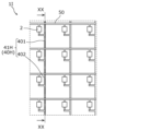
- FIG. FIG. 2 is a top view of the wiring board 1.
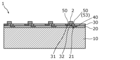
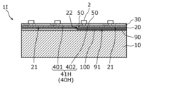
- FIG. 3A is a cross-sectional view of the wiring board 1 along line IIIA-IIIA in FIG. 2
- FIG. 3B is a cross-sectional view of the wiring board 1 along line IIIB-IIIB in FIG. 1 to 3B show a part of the wiring board 1. As shown in FIG.
- the wiring board 1 includes a film 10 , a first insulating layer 20 , a second insulating layer 30 , first wirings 40 and second wirings 50 .
- the wiring board 1 is a multilayer wiring board in which the first wirings 40 and the second wirings 50 are positioned at different heights.
- the wiring board 1 in this embodiment further includes a circuit element 2 .
- the wiring board 1 includes a plurality of circuit elements 2 .
- the wiring board 1 has the circuit element 2 mounted thereon, but the wiring board 1 may have no circuit element 2 mounted thereon. Moreover, the wiring board 1 on which the circuit element 2 is mounted as in the present embodiment is a circuit module. As will be described later, in this embodiment, the circuit element 2 is an LED light source, so the wiring board 1 is a light source module.
- the film 10 is a resin base film of the wiring board 1 .
- the film 10 is a translucent base material and is made of a translucent resin material.
- the film 10 is preferably a transparent base material with high transmittance so that the other side can be seen through.
- the film 10 is a transparent PET film made of PET (polyethylene terephthalate).
- the resin material forming the film 10 is not limited to PET, and resin materials such as cycloolefin resin, polycarbonate resin, and acrylic resin may be used.
- the film 10 may be a rigid base material or a flexible base material.
- the first insulating layer 20 is positioned above the film 10 and laminated on the film 10 .
- the first insulating layer 20 is formed directly above the film 10 . Therefore, the bottom surface of the first insulating layer 20 is in contact with the top surface of the film 10 .
- the second insulating layer 30 is located above the first insulating layer 20 and laminated on the first insulating layer 20 .
- the second insulating layer 30 is formed directly above the first insulating layer 20 . Therefore, the bottom surface of the second insulating layer 30 is in contact with the top surface of the first insulating layer 20 .
- the wiring board 1 two insulating layers, the first insulating layer 20 and the second insulating layer 30 , are laminated on the film 10 .
- the first insulating layer 20 is a lower insulating layer
- the second insulating layer 30 is an upper insulating layer.
- the second insulating layer 30 is the uppermost layer of the wiring board 1 .
- the first insulating layer 20 and the second insulating layer 30 are resin layers made of an insulating resin material.
- the first insulating layer 20 and the second insulating layer 30 are made of translucent resin material.
- the first insulating layer 20 and the second insulating layer 30 are made of a transparent resin material.
- the first insulating layer 20 and the second insulating layer 30 are made of a resin material having insulating properties and optical transparency.
- the resin material forming the first insulating layer 20 and the second insulating layer 30 is a thermosetting resin or an ultraviolet curable resin material.
- the first insulating layer 20 and the second insulating layer 30 may be made of the same resin material, or may be made of different resin materials.
- the first insulating layer 20 has a first groove portion 21 .
- the first groove portion 21 is a groove-shaped concave portion formed so that the surface of the first insulating layer 20 is depressed, and is formed in an elongated shape. Specifically, the first groove portion 21 is formed linearly.
- the first groove portion 21 has a first bottom surface and a first side surface continuously connected to the first bottom surface.
- the cross-sectional shape of first groove portion 21 when cut along a cross section orthogonal to the longitudinal direction of first groove portion 21 is rectangular.
- the first groove portion 21 has a planar first bottom surface and a pair of planar first side surfaces that are opposed to each other.
- the first insulating layer 20 is a single layer made of a single material, the first insulating layer 20 is made of the same material on the first bottom surface and the first side surface of the first groove portion 21 . That is, in the first insulating layer 20, the material forming the first bottom surface and the material forming the first side surface are the same.
- a conductive first wiring 40 is formed in the first trench 21 of the first insulating layer 20 .
- the first wiring 40 is embedded inside the first groove portion 21 . That is, the first insulating layer 20 is a groove-forming layer in which the first grooves 21 in which the first wirings 40 are embedded are formed.
- the first wiring 40 formed in the first insulating layer 20, which is a lower insulating layer, is a lower layer wiring.
- the first wiring 40 is a conductor made of a conductive material.
- the first wiring 40 is a metal wiring made of a metal material such as copper, aluminum, or silver.
- the first wiring 40 is a copper wiring made of copper.
- the first wiring 40 may be made of copper alone or may be made of a copper alloy. Note that the first wiring 40 may be made of a conductive material other than copper.
- the thickness of the first wiring 40 embedded in the first groove 21 is thinner than the thickness of the first insulating layer 20.
- the first wiring 40 is formed in an elongated shape like the first groove portion 21 . Specifically, the first wiring 40 is formed in a straight line like the first groove portion 21 .
- the first wiring 40 has at least three surfaces.
- the cross-sectional shape of the first wiring 40 when cut along a cross section orthogonal to the longitudinal direction of the first wiring 40 is the same as the cross-sectional shape of the first groove portion 21 . Therefore, in the present embodiment, the cross-sectional shape of the first wiring 40 is rectangular.
- the first wiring 40 has four surfaces: a lower surface, a pair of side surfaces, and an upper surface.
- the bottom surface and the pair of side surfaces of the first wiring 40 are in contact with the bottom surface and the pair of side surfaces of the first groove portion 21, respectively.
- the top surface of the first wiring 40 may or may not be flush with the top surface of the first insulating layer 20 .
- the first wiring 40 may be formed so that the central portion of the line width is slightly recessed. Therefore, the top surface of the first wiring 40 may or may not be in contact with the bottom surface of the second insulating layer 30 . As will be described later, part of the upper surface of the first wiring 40 is in contact with the second wiring 50 .
- the second insulating layer 30 has a second groove portion 31 .
- the second groove portion 31 is a groove-shaped concave portion formed so that the surface of the second insulating layer 30 is depressed, and is formed in an elongated shape. Specifically, the second groove portion 31 is formed linearly.
- the second groove portion 31 has a second bottom surface and a second side surface continuously connected to the second bottom surface.
- the second groove portion 31 has a rectangular cross-sectional shape when cut along a cross section orthogonal to the longitudinal direction of the second groove portion 31 .
- the second groove portion 31 has a planar second bottom surface and a pair of planar second side surfaces that are opposed to each other.
- the second insulating layer 30 is a single layer made of a single material, the second bottom surface and the second side surface of the second groove portion 31 are made of the same material. That is, in the second insulating layer 30, the material forming the second bottom surface and the material forming the second side surfaces are the same.
- the second insulating layer 30 has an opening 32 located above the first wiring 40 .
- the opening 32 is a through hole penetrating through the second insulating layer 30 . Therefore, the depth of the opening 32 is deeper than the depth of the second groove 31 .
- a conductive second wiring 50 is formed in the second groove 31 and the opening 32 in the second insulating layer 30 .
- the second wiring 50 is embedded inside the second groove 31 and inside the opening 32 .
- the second insulating layer 30 is a groove forming layer in which the second groove portion 31 in which the second wiring 50 is embedded is formed.
- the second wiring 50 formed in the second insulating layer 30, which is an upper insulating layer, is an upper layer wiring.
- the second wiring 50 is a conductor made of a conductive material.
- the second wiring 50 is a metal wiring made of a metal material such as copper, aluminum, or silver.
- the second wiring 50 is made of the same conductive material as the first wiring 40 . Therefore, the second wiring 50 is a copper wiring made of copper.
- the second wiring 50 may be made of copper alone or may be made of a copper alloy.
- the second wiring 50 may be made of a conductive material other than copper. Also, the second wiring 50 may be made of a material different from that of the first wiring 40 .
- the thickness of the second wiring 50 embedded in the second groove 31 is thinner than the thickness of the second insulating layer 30.
- the thickness of the second wiring 50 embedded in the opening 32 is the same as the thickness of the second insulating layer 30, but is not limited to this.
- the thickness of the second wiring 50 and the thickness of the second insulating layer 30 may differ.
- the thickness of at least part of the second wiring 50 formed in the second groove portion 31 may be thinner than the thickness of the second insulating layer 30 .
- the second wiring 50 formed in the second groove portion 31 is formed in an elongated shape like the second groove portion 31 . Specifically, the second wiring 50 formed in the second groove portion 31 is formed in a straight line like the second groove portion 31 . In addition, although the second wiring 50 formed in the opening 32 is formed in a land shape when viewed from above, it may be formed in a straight line.
- the second wiring 50 formed in the second groove portion 31 has at least three surfaces.
- the cross-sectional shape of the second wiring 50 formed in the second groove portion 31 is the same as the cross-sectional shape of the second groove portion 31 when cut along a cross section perpendicular to the longitudinal direction of the second wiring 50 . Therefore, in the present embodiment, the cross-sectional shape of the second wiring 50 formed in the second groove portion 31 is rectangular.
- the second wiring 50 formed in the second groove 31 has four surfaces, a lower surface, a pair of side surfaces, and an upper surface.
- the bottom surface and the pair of side surfaces of the second wiring 50 are in contact with the bottom surface and the pair of side surfaces of the second groove portion 31, respectively.
- the upper surface of the second wiring 50 formed in the second groove portion 31 may or may not be flush with the upper surface of the second insulating layer 30 .
- the second wiring 50 may be formed so that the central portion of the line width is slightly recessed.
- the cross-sectional shape of the second wiring 50 formed in the opening 32 is also rectangular.
- the upper surface of the second wiring 50 formed in the opening 32 may also be flush with the upper surface of the second insulating layer 30, or may not be flush.
- the second wiring 50 formed in the opening 32 may be formed so that the central portion of the line width is slightly recessed.
- the lower surface of the second wiring 50 formed in the opening 32 and the upper surface of the first wiring 40 are joined. That is, the bottom surface of the second wiring 50 formed in the opening 32 is in contact with the top surface of the first wiring 40 . Therefore, the second wiring 50 embedded in the opening 32 is a via, and the first wiring 40 and the second wiring 50 are connected through the opening 32 (via hole). Thus, the opening 32 formed in the second insulating layer 30 functions as a contact portion that connects the first wiring 40 and the second wiring.
- the first wiring 40 includes a plurality of linear first main wirings 41 extending in the column direction (first direction) and a plurality of first branch wirings 42 branching from the first main wirings 41 .
- the first branch wiring 42 extends linearly in the row direction (second direction) orthogonal to the column direction.
- the second wiring 50 includes a plurality of linear second main wirings 51 extending in the row direction (second direction), a plurality of second branch wirings 52 branching from the second main wirings 51, and a contact wiring 53 connected to the first wiring 40.
- the second branch wiring 52 extends linearly in the column direction (first direction).
- the contact wiring 53 is spaced apart from the second branch wiring 52 in the column direction, and is electrically connected to the second branch wiring 52 via the circuit element 2 .
- a plurality of first main wirings 41 of the first wiring 40 and a plurality of second main wirings 51 of the second wiring 50 are three-dimensionally crossed.
- the first branch wiring 42 of the first wiring 40 is connected to the contact wiring 53 of the second wiring 50 .
- the first branch wiring 42 of the first wiring 40 is connected to the contact wiring 53 through the opening 32 formed in the second insulating layer 30 .
- a plurality of circuit elements 2 are arranged in a matrix. Specifically, the plurality of circuit elements 2 are arranged in the vicinity of an intersection point where the first main wiring 41 of the first wiring 40 and the second main wiring 51 of the second wiring 50 cross each other.
- the circuit element 2 has a pair of electrodes. One of the pair of electrodes of the circuit element 2 is connected to the second branch wiring 52 of the second wiring 50 . The other of the pair of electrodes of the circuit element 2 is connected to the contact wiring 53 connected to the first wiring 40 . Thereby, the pair of electrodes of the circuit element 2 are connected to the pair of the first wiring 40 and the second wiring 50 .
- the circuit element 2 is a light emitting element.
- the circuit element 2 is an LED light source made up of LEDs.
- an SMD (Surface Mount Device) type LED light source in which an LED chip is mounted in a package can be used.
- An SMD type LED light source is provided with an anode electrode and a cathode electrode on the back surface.
- the anode electrode of the LED light source is connected to the second branch wiring 52 of the second wiring 50, and the cathode electrode of the LED light source is connected to the contact wiring 53 connected to the first wiring 40.
- the wiring board 1 configured in this manner can drive a plurality of circuit elements 2 by using a column driving driver IC that supplies current to the first wirings 40 having a plurality of first main wirings 41 extending in the column direction and a row driving driver IC that supplies currents to the second wirings 50 having a plurality of second main wirings 51 extending in the row direction.
- the circuit element 2 is an LED light source, it is possible to control the lighting and extinguishing of a plurality of LED light sources by using a column driving driver IC and a row driving driver IC. Specifically, a plurality of LED light sources can be individually (selectively) controlled by a simple matrix driving method. By controlling the lighting and extinguishing of the plurality of LED light sources arranged in a matrix in this manner, an image can be displayed using the plurality of LED light sources as pixels.
- the wiring board 1 according to this embodiment is a display device that can be used for a display device.
- the wiring substrate 1 in this embodiment is a transparent wiring substrate and can be used for a transparent display device.
- FIGS. 4A to 4H are diagrams for explaining each step in the method of manufacturing wiring board 1 according to the first embodiment.
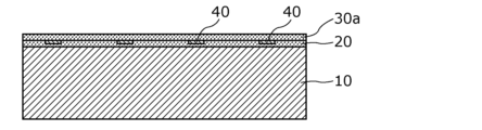
- the film 10 is prepared, and the first groove forming layer 20a made of a resin material is arranged on the film 10. Then, as shown in FIG. In this embodiment, a PET film is used as the film 10 . Then, an uncured (liquid) resin material having insulating and light-transmitting properties was applied to the surface of the film 10 as the first groove forming layer 20a.
- the liquid resin material forming the first groove forming layer 20a can be applied using a coating device such as a dispenser.
- the first insulating layer 20 having the first grooves 21 is formed by forming the first grooves 21 in the first groove forming layer 20a.
- the uneven structure of the first transfer plate is transferred to the first groove-forming layer 20a. That is, the first grooves 21 corresponding to the projections of the uneven structure of the first transfer plate are formed in the first groove forming layer 20a. Then, the first groove forming layer 20a, which is a liquid resin material, is cured while the first transfer plate is pressed against the first groove forming layer 20a. After that, the first transfer plate is peeled off from the film 10 . Thereby, as shown in FIG. 4B, the first insulating layer 20 in which the first groove portion 21 is formed can be formed.
- the first wiring 40 is formed in the first trench 21 of the first insulating layer 20. Then, as shown in FIG. Specifically, a first wiring 40 made of copper is formed so as to fill the first groove portion 21 .
- the first wiring 40 can be formed by embedding a conductive material (plating material) such as copper in the first groove portion 21 by plating.
- the first wiring 40 may be formed by applying a conductive material to the first groove portion 21 .
- the conductive material protrudes from the first groove 21
- only the protruding conductive material is removed, or the protruding conductive material and the surface layer of the first insulating layer 20 are removed together, thereby forming the first wiring 40 embedded in the first groove 21 so that the upper surface of the first insulating layer 20 and the upper surface of the first wiring 40 are flush with each other.
- the upper surface of the first insulating layer 20 and the upper surface of the first wiring 40 may not be flush with each other.
- a second groove forming layer 30a made of a resin material is arranged on the first insulating layer 20 having the first wiring 40 formed in the first groove portion 21. Then, as shown in FIG.
- an uncured (liquid) resin material having insulating and light-transmitting properties is applied onto the surface of the first insulating layer 20 as the second groove-forming layer 30a.
- the liquid resin material forming the second groove forming layer 30a can be applied using a coating device such as a dispenser.
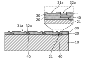
- a first concave portion 31a corresponding to the second groove portion 31 and a second concave portion 32a corresponding to the opening portion 32 are formed in the second groove forming layer 30a, thereby forming the second insulating layer 30 having the first concave portion 31a and the second concave portion 32a.
- a second transfer plate which is a mold having an uneven structure, is pressed against the surface of the second groove-forming layer 30a, which is a liquid resin material, to transfer the uneven structure of the second transfer plate to the second groove-forming layer 30a. That is, the first concave portions 31a and the second concave portions 32a corresponding to the first convex portions and the second convex portions of the concave-convex structure of the second transfer plate are formed in the second groove forming layer 30a. Then, the second groove forming layer 30a, which is a liquid resin material, is cured while the second transfer plate is pressed against the second groove forming layer 30a. After that, the second transfer plate is peeled off from the film 10 .
- the second insulating layer 30 in which the first concave portion 31a and the second concave portion 32a are formed can be formed.
- the second concave portion 32 a corresponds to the opening portion 32 , so it is formed above the first wiring 40 .
- the depth of the second recess 32a is deeper than the depth of the first recess 31a. That is, the depth of the second recess 32a corresponding to the opening 32 is made deeper than the depth of the first recess 31a corresponding to the second groove 31 in advance.
- the first recessed portion 31a and the second recessed portion 32a having different depths can be formed, for example, by making the heights of the protrusions and recesses of the mold (transfer plate) different in advance.
- the second groove 31 and the opening 32 are formed in the second insulating layer 30 by removing the bottoms of the first recess 31a and the second recess 32a.
- the entire surface layer of the second insulating layer 30 can be removed by ashing the entire second insulating layer 30 that has been previously made deeper than the depth of the first recess 31a.
- the bottom of the first recess 31a can be deepened to form the second groove 31, and the bottom of the second recess 32a can be penetrated to form the opening 32.
- the opening 32 penetrates the second insulating layer 30 .
- the entire surface layer of the second insulating layer 30 can be removed by oxygen plasma, ions or ozone.
- only the bottoms of the first recessed portion 31a and the second recessed portion 32a may be removed by a short-wavelength laser with a wavelength of 172 nm or an excimer laser.
- the second wiring 50 is formed in the second trench 31 and the opening 32 of the second insulating layer 30 . Specifically, the second wiring 50 is formed so as to fill the second groove portion 31 and the opening portion 32 .
- the second wiring 50 can be formed by embedding a conductive material (plating material) in the second groove 31 and the opening 32 by a plating method, or the second wiring 50 can be formed by applying a conductive material to the second groove 31.
- the conductive material protrudes from the second groove 31, only the protruding conductive material is removed, or the protruding conductive material and the surface layer of the second insulating layer 30 are removed together, thereby forming the second wiring 50 embedded in the second groove 31 and the opening 32 so that the upper surface of the second insulating layer 30 and the upper surface of the second wiring 50 are flush with each other. If the second wiring 50 is formed such that the central portion of the width of the second wiring 50 is slightly recessed, the upper surface of the second insulating layer 30 and the upper surface of the second wiring 50 may not be flush with each other.
- the wiring board 1a which is a multilayer wiring board in which the first wirings 40 and the second wirings 50 are formed in different wiring layers and the first wirings 40 and the second wirings 50 are partially joined, can be formed.
- the circuit element 2 is mounted on the wiring board 1a on which the first wiring 40 and the second wiring 50 are formed.
- the wiring board 1 on which the circuit element 2 is mounted can be obtained.
- an LED light source is mounted as the circuit element 2 .
- the electrode of the LED light source and the second wiring 50 are joined by soldering or the like.
- the present invention when forming the second groove 31 and the opening 32 in the second insulating layer 30, as shown in FIG. 4E, the first recess 31a and the second recess 32a having different depths are formed in advance, but the present invention is not limited to this.
- a first concave portion 31a and a second concave portion 32a having the same depth are formed, and the bottom of only the second concave portion 32a is removed by a laser to penetrate the second insulating layer 30, thereby forming the second groove portion 31 and the opening portion 32. 5 corresponds to the step of FIG. 4E (the step of forming the first concave portion 31a and the second concave portion 32a in the second insulating layer 30).
- FIG. 6 is a perspective view of a wiring board 1X of Comparative Example 1.
- FIG. 7 is a top view of a wiring substrate 1X of Comparative Example 1.
- FIG. 8 is a cross-sectional view of the wiring board 1X of Comparative Example 1 along line VIII-VIII of FIG.
- the wiring board 1X of Comparative Example 1 includes a film 10X, an insulating layer 20X formed on the film 10X, and wiring 40X formed in the grooves 21X of the insulating layer 20X.
- the wiring board 1X of Comparative Example 1 further includes a plurality of LED light sources 2X arranged in a matrix.
- the wiring 40X is formed by an imprint method.
- the wiring 40X is formed on a single insulating layer 20X. Therefore, if the wiring 40X is formed in a pattern for matrix-driving the plurality of LEDs 2X arranged in a matrix, as shown in FIGS.
- the wiring 40X occupies a large proportion. That is, the area of the wiring 40X becomes large when the wiring board 1X is viewed from above. As a result, the pitch of the LED light sources 2X cannot be reduced, and a high-definition image cannot be displayed.
- the wiring board 1X of Comparative Example 1 is a transparent device in which the film 10, the first insulating layer 20, and the second insulating layer 30 are transparent. However, if there is an area where a large number of wirings 40X must be formed between the adjacent LED light sources 2X, the wirings 40X are light-shielding members, so the transmittance of the wiring board 1 decreases.
- the first insulating layer 20 and the second insulating layer 30 are laminated above the resin film 10, the first wiring 40 is formed in the first groove 21 of the first insulating layer 20, which is the lower insulating layer, and the second wiring 50 is formed in the second groove 31 and the opening 32 of the second insulating layer 30, which is the upper insulating layer.
- the upper surface of the first wiring 40 as the lower layer wiring and the lower surface of the second wiring 50 as the upper layer wiring formed in the opening 32 of the second insulating layer 30 are joined.
- the wiring of the wiring board 1 can be divided into the first wiring 40 and the second wiring 50 in the two layers of the first insulating layer 20 and the second insulating layer 30 .
- the ratio occupied by the wiring can be reduced when the wiring board 1 is viewed from above. That is, it is possible to reduce the wiring area when the wiring substrate 1 is viewed from above.
- the circuit elements 2 are arranged in a matrix on the wiring board 1, compared with the wiring board 1X of Comparative Example 1, the area of the entire wiring when the wiring board 1 is viewed from above can be reduced.
- the transmittance of the wiring board 1 can be improved by reducing the ratio of wiring when the wiring board 1 is viewed from above.
- the transmittance of the region where the first wiring 40 and the second wiring 50 are not formed is 80% or more, and can be further increased to 85%.
- the second wiring 50 buried in the second groove 31 and extending linearly and the second wiring 50 buried in the opening 32 and serving as vias can be formed from the same material at the same time.
- the structure of the wiring board 1 according to the present embodiment makes it possible to easily increase the thickness of the first wirings 40 and the second wirings 50, so that the resistance values of the first wirings 40 and the second wirings 50 can be reduced.
- At least one of the first wiring 40 and the second wiring 50 may have a black layer formed on part or the entire surface thereof.
- the first wiring 40 and the second wiring 50 have at least three surfaces, and a black layer may be formed on at least one of the three surfaces. In this case, a black layer may be formed on the entire surface of at least one of the first wiring 40 and the second wiring 50 .
- FIG. 9 is a cross-sectional view of wiring board 1A according to a modification of the first embodiment.
- FIG. 9 shows an enlarged peripheral structure of one circuit element 2 .
- black layers are formed on all surfaces of the first wirings 40 and the second wirings 50, respectively.
- a black layer 61 is formed on each of the lower surface, the pair of side surfaces, and the upper surface of the first wiring 40 . Therefore, the black layer 61 is formed on the entire inner surface of the first groove portion 21 of the first insulating layer 20 .
- a black layer 62 is formed on each of the lower surface, the pair of side surfaces, and the upper surface of the second wiring 50 . Therefore, the black layer 62 is formed on the entire inner surface of the second groove portion 31 of the second insulating layer 30 .
- the black layer 61 formed on the surface of the first wiring 40 is preferably formed on at least the upper surface of the first wiring 40 .
- the black layer 62 formed on the surface of the second wiring 50 is preferably formed on at least the upper surface of the second wiring 50 .
- the black layer 61 covering the first wiring 40 can be formed by the method shown in FIG. 10A and 10B are diagrams for explaining a method of forming the black layer 61 on the first wiring 40.
- FIG. 10A and 10B are diagrams for explaining a method of forming the black layer 61 on the first wiring 40.
- a black film 61a is formed so as to cover the inner surface of the first groove 21, as shown in FIG.
- the black layer 61a is, for example, a layer containing at least one metal selected from the group consisting of Ti, Al, V, W, Ta, Si, Cr, Ag, Mo, Cu, and Zn.
- the black film 61a is formed over the entire surface of the portion of the first insulating layer 20 where the first groove portion 21 is formed and the portion where the first groove portion 21 is not formed.
- the black film 61a can be formed by sputtering, for example.
- a metal film 40M is formed on the black film 61a so as to fill the first groove portion 21 with the black film 61a formed on the inner surface.
- a metal film 40M made of a plating film is formed on the black film 61a by forming a copper film by plating using the black film 61a as a base film (nucleus).
- the metal film 40M is removed so as to leave the metal film 40M with which the first groove 21 is filled.
- the metal film 40M is removed until the black film 61a formed on the first insulating layer 20 in the portion where the first groove portion 21 is not formed is removed.
- the black film 61a formed on the inner surface of the first groove portion 21 remains, and the metal film 40M embedded in the first groove portion 21 remains.
- the metal film 40M embedded in the first groove portion 21 becomes the first wiring 40.
- the upper surface layer of the first wiring 40a formed in the first groove portion 21 is blackened to form a blackening film 61b.
- the upper layer portion of the first wiring 40a (plated film) is replaced with a blackened layer.
- the black layer 61 can be formed so as to cover the entire four surfaces of the first wiring 40.
- the black layer 61 thus formed is composed of a black film 61 a covering the lower surface and a pair of side surfaces of the first wiring 40 and a blackened film 61 b covering the upper surface of the first wiring 40 .
- the black layer 62 covering the second wiring 50 can be formed by the same method as the black layer 61 .
- FIG. 11 is a cross-sectional view of wiring board 1B according to the second embodiment.
- the wiring board 1B according to the present embodiment and the wiring board 1 according to the first embodiment are different in the configuration of the second wiring 50B.
- the second wirings 50 are made of one kind of material, but in the wiring board 1B according to the present embodiment, the second wirings 50B are made of two or more kinds of materials.
- the second wiring 50B is formed in the second groove 31 and the opening 32 of the second insulating layer 30.
- a second wiring 50B formed in each of the second groove portion 31 and the opening portion 32 includes a first conductive layer 510 and a second conductive layer 520 .
- the first conductive layer 510 is the bottom layer of the second wiring 50B, and is formed in each of the second grooves 31 and the openings 32 . Therefore, the lower surface of the first conductive layer 510 formed in the opening 32 is the lower surface of the second wiring 50B and is joined to the upper surface of the first wiring 40 formed in the first groove 21 of the first insulating layer 20.
- a second conductive layer 520 is formed on the first conductive layer 510 .
- the second conductive layer 520 is one or more, and is composed of one or more.
- the second conductive layer 520 is composed of two layers, a lower conductive layer 521 and an upper conductive layer 522 .
- a lower conductive layer 521 is formed on the first conductive layer 510 and an upper conductive layer 522 is formed on the lower conductive layer 521 .
- the second conductive layer 520 may be formed without protruding from the second groove 31 and the opening 32, but may be formed to protrude from the second groove 31 and the opening 32. In this embodiment, the second conductive layer 520 protrudes from the second groove 31 and the opening 32 . Specifically, in the second conductive layer 520, part of the lower conductive layer 521 protrudes from the second groove 20 and the opening 32, and all of the upper conductive layer 522 protrudes from the second groove 31 and the opening 32.
- the first conductive layer 510 and the second conductive layer 520 are made of a conductive material such as a metal material, but the first conductive layer 510 and the second conductive layer 520 are made of a different material.
- first conductive layer 510 is a copper layer made of copper.
- the lower conductive layer 521 of the second conductive layer 520 is a nickel layer made of nickel, and the upper conductive layer 522 of the second conductive layer 520 is a gold layer made of gold. That is, the second wiring 50B has a layered structure of a copper layer, a nickel layer, and a gold layer. In this case, the nickel layer and the gold layer can be formed by plating.
- the first wiring 40 formed in the first groove portion 21 of the first insulating layer 20 is composed only of copper, as in the first embodiment. That is, the first wiring 40 in the present embodiment is made of one type of material. Therefore, in the present embodiment, the first wiring 40 and the second wiring 50B are made of different conductive materials.
- the first insulating layer 20 and the second insulating layer 30 are laminated above the resin film 10, the first wiring 40 is formed in the first groove 21 of the first insulating layer 20, which is the lower insulating layer, and the second wiring 50B is formed in the second groove 31 and the opening 32 of the second insulating layer 30, which is the upper insulating layer.
- the upper surface of the first wiring 40 as the lower wiring and the lower surface of the second wiring 50B as the upper wiring formed in the opening 32 of the second insulating layer 30 are joined.
- first wiring 40 and second wiring 50B are made of different conductive materials.
- the conductive material of the second wiring 50B can be selected so as to improve the bondability between the electrodes of the circuit element 2 and the second wiring 50B.
- the second wiring 50B is composed of a first conductive layer 510 made of copper and a second conductive layer 520 formed on the first conductive layer 510.
- the second conductive layer 520 is composed of a lower conductive layer 521 made of a nickel layer and an upper conductive layer 522 made of a gold layer.
- the first wiring 40 is made of one type of material, and only the second wiring 50B is made of two or more types of material, but the present invention is not limited to this.
- each of the first wiring 40 and the second wiring 50B may be made of two or more kinds of materials. That is, at least one of the first wiring 40 and the second wiring 50B should be made of two or more kinds of materials.
- the entire wiring of the wiring board 1B including the first wiring 40 and the second wiring 50B may be made of two or more kinds of metal materials.
- FIG. 12 is a cross-sectional view of wiring board 1C according to the third embodiment.
- the wiring board 1C according to the present embodiment has a configuration in which the wiring board 1 according to the first embodiment is further provided with a third insulating layer 70 .
- the third insulating layer 70 is located above the second insulating layer 30 and laminated on the second insulating layer 30 .
- the third insulating layer 70 is formed directly above the second insulating layer 30 . Therefore, the bottom surface of the third insulating layer 70 is in contact with the top surface of the second insulating layer 30 .
- the three insulating layers of the first insulating layer 20 , the second insulating layer 30 and the third insulating layer 70 are laminated on the film 10 .
- the third insulating layer 70 is the uppermost layer of the wiring board 1C.
- the third insulating layer 70 is made of an insulating resin material or an insulating inorganic material.
- the third insulating layer 70 is made of translucent resin material or translucent inorganic material.
- the third insulating layer 70 is made of a transparent resin material or a transparent inorganic material.
- the third insulating layer 70 is made of an insulating resin material
- the same material as the first insulating layer 20 and the second insulating layer 30 can be used as the material of the third insulating layer 70 .
- the third insulating layer 70 is made of an insulating inorganic material, a silicon dioxide film or the like can be used as the third insulating layer 70 .
- the third insulating layer 70 has through holes 71 .
- the through holes 71 can be formed after the third insulating layer 70 is deposited.
- a through hole 71 formed in the third insulating layer 70 is formed on the second wiring 50 . At least part of the second wiring 50 is exposed from the through hole 71 . That is, in the present embodiment, the third insulating layer 70, which is the uppermost layer of the wiring board 1C, is provided with the through holes 71 that expose at least part of the second wirings 50 formed in the second grooves 31.
- the through hole 71 is a depression (recess) formed in the third insulating layer 70 which is the uppermost layer.
- a circuit element 2 is arranged in the through hole 71 .
- a plurality of through holes 71 are formed in the third insulating layer 70 , and the circuit element 2 is arranged in each through hole 71 .
- the through hole 71 is a recess into which the circuit element 2 is fitted.
- the shape of the through hole 71 when viewed from above is rectangular or circular, and the side surface of the through hole 71 surrounds the circuit element 2 . Note that there is a gap between the side surface of the through hole 71 and the side surface of the circuit element 2 .
- the electrodes of the circuit element 2 arranged in the through holes 71 are joined to the second wirings 50 in the same manner as in the first embodiment.
- the through-holes 71 are formed only where the circuit elements 2 are present. That is, the through hole 71 is formed only in the portion (electrode portion) of the second wiring 50 where the circuit element 2 is mounted.
- the first insulating layer 20 and the second insulating layer 30 are laminated above the resin film 10, the first wiring 40 is formed in the first groove 21 of the first insulating layer 20, and the second wiring 50 is formed in the second groove 31 and the opening 32 of the second insulating layer 30.
- the upper surface of the first wiring 40 and the lower surface of the second wiring 50 are joined together.
- the third insulating layer 70 is further formed on the second insulating layer 30 .
- the third insulating layer 70 functions as a protective layer, thereby improving the reliability of the wiring board 1C.
- through holes 71 are formed in the third insulating layer 70, which is the uppermost layer of the wiring board 1C.
- the through hole 71 is formed in an element mounting portion on which the circuit element 2 is mounted. That is, through holes 71 are formed in the third insulating layer 70, which is the uppermost layer, as concave portions in which the circuit elements 2 are fitted.
- the circuit element 2 can be easily fitted into the through hole 71 when the circuit element 2 is mounted on the wiring board 1C. As a result, the circuit element 2 can be easily mounted at a predetermined position on the wiring board 1C, and displacement of the circuit element 2 during mounting can be suppressed.
- the through holes 71 are formed only in the portion (electrode portion) of the second wiring 50 where the circuit element 2 is mounted. Accordingly, corrosion of the second wiring 50 can be suppressed.
- the side surface of the through hole 71 formed in the third insulating layer 70 is a vertical surface perpendicular to the upper surface of the third insulating layer 70, but it is not limited to this.
- the side surface of the through hole 71 may be an inclined surface that is inclined with respect to the upper surface of the third insulating layer 70.
- the inclined surface of the through hole 71 is preferably a tapered surface such that the opening area gradually increases along the depth direction of the third insulating layer 70 .
- electrodes 80 joined to the second wirings 50 may be formed in the through holes 72 of the third insulating layer 70 .
- the electrodes 80 are formed on the uppermost layer of the wiring board 1E.
- the electrode 80 is formed, for example, so as to be embedded in the through hole 72, and the surface is exposed. As a result, the second wiring 50 is not exposed, and corrosion of the second wiring 50 can be suppressed.
- a circuit element 2 is connected to the electrode 80 . Therefore, the electrode 80 is formed in a land shape corresponding to the electrode of the circuit element 2 .
- the electrode 80 formed in the through hole 71 of the third insulating layer 70 may be made of a material different from that of the second wiring 50 .
- the conductive material of the electrodes 80 can be selected so as to improve the bondability between the electrodes of the circuit element 2 and the electrodes 80 of the uppermost layer.
- the electrodes 80F formed in the through holes 72 of the third insulating layer 70 may include a first electrode layer 81 and a second electrode layer 82 laminated on the first electrode layer 81.
- the first electrode layer 81 bonded to the second wiring 50 is a nickel layer made of nickel
- the second electrode layer 82 bonded to the first electrode layer 81 is a gold layer made of gold.
- the nickel layer and the gold layer can be formed by a plating method.
- FIG. 16 is a cross-sectional view of wiring board 1G according to the fourth embodiment. Note that the cross-sectional view of FIG. 16 corresponds to the cross-sectional view of FIG. 3B in the wiring board 1 of the first embodiment.
- the width of the first wiring 40 and the width of the second wiring 50 are the same at the joint surface between the first wiring 40 and the second wiring 50. However, as shown in FIG.
- the widths of the first wiring 40G and the second wiring 50G are constant in the thickness direction as in the first embodiment. Therefore, the width of the first wiring 40G and the width of the second wiring 50G differ not only in the joint surface between the first wiring 40 and the second wiring 50, but also in the entire width of the first wiring 40G and the entire width of the second wiring 50G.
- the width of the second wiring 50G positioned in the upper layer is preferably larger than the width of the first wiring 40G positioned in the lower layer.
- the width of the first wiring 40G is the same as the width of the first wiring 40 in the first embodiment, and the width of the second wiring 50G is larger than the width of the second wiring 50 in the first embodiment, but the width is not limited to this.
- the first insulating layer 20 and the second insulating layer 30 are laminated above the resin film 10 in the same manner as in the first embodiment, the first wiring 40G is formed in the first groove 21 of the first insulating layer 20, and the second wiring 50G is formed in the second groove 31 and the opening 32 of the second insulating layer 30. Then, the upper surface of the first wiring 40G and the lower surface of the second wiring 50G are joined.
- the width of the first wiring 40G and the width of the second wiring 50G are different at the joint surface between the first wiring 40G and the second wiring 50G.
- the width of the second wiring 50G located in the upper layer is larger than the width of the first wiring 40G located in the lower layer.
- the element connectivity between the second wiring 50G and the circuit element 2 can be improved. In other words, even if the circuit element 2 is misaligned during mounting, the bonding state between the electrodes of the circuit element 2 and the second wiring 50G can be ensured.
- FIG. 17 is a top view of wiring board 1H according to the fifth embodiment.
- FIG. 18 is a cross-sectional view of the wiring board 1H taken along line XVIII--XVIII of FIG. 17 and 18 show the configuration of part of the wiring board 1H.
- the wiring board 1H according to the present embodiment further includes a lower insulating layer 90 located below the first insulating layer 20 in addition to the wiring board 1 according to the first embodiment.
- the lower insulating layer 90 can be formed using the same material as the first insulating layer 20 .
- a groove portion 91 is formed in the lower insulating layer 90 .
- the groove portion 91 can be formed by the same method as the first groove portion 21 of the first insulating layer 20 .
- a conductive branch wiring 100 is formed in the groove 91 of the lower insulating layer 90 .
- the branch wiring 100 can be formed using the same conductive material as the first wiring 40 in the first embodiment.
- the branch wiring 100 is a copper wiring made of copper.
- the first wiring 40H in the present embodiment is divided into a first divided wiring 401 and a second divided wiring 402 . Specifically, each first main wiring 41 ⁇ /b>H of the plurality of first wirings 40 ⁇ /b>H is divided into a first divided wiring 401 and a second divided wiring 402 .
- An opening 22 is formed in the first insulating layer 20 in addition to the first groove 21 .
- the opening 22 in the first insulating layer 20 can be formed in the same manner as the opening 32 in the second insulating layer 30 .
- the first wiring 40H is formed in the first groove portion 21 of the first insulating layer 20 as in the first embodiment. Specifically, each of the first divided wiring 401 and the second divided wiring 402 is formed in the first groove portion 21 . In the present embodiment, a portion of first wiring 40H is formed in opening 22 of first insulating layer 20 . Specifically, the first split wiring 401 of the first wiring 40H is formed in the opening 22 of the first insulating layer 20 .
- the lower surface of the first wiring 40H (first divided wiring 401) formed in the opening 22 of the first insulating layer 20 and the upper surface of the branch wiring 100 are joined. That is, the lower surface of the first wiring 40H formed in the opening 22 is in contact with the upper surface of the branch wiring 100.
- the first divided wiring 401 of the first wiring 40H formed in the opening 22 is a contact portion (via), and the first divided wiring 401 and the branch wiring 100 are connected through the opening 22 (via hole).
- the first split wiring 401 of the first wiring 40H is connected to the branch wiring 100 formed in the groove 91 of the lower insulating layer 90 via the opening 22 formed in the first insulating layer 20 . That is, the branch wiring 100 functions as the first wiring 40H.
- the first wiring 40 ⁇ /b>H has a portion branched in the thickness direction, and the branch wiring 100 forms a two-story structure.
- the current flowing through the first wiring 40H can be distributed.
- the current flowing through the first wiring 40 ⁇ /b>H can be distributed to the wiring path including the first split wiring 401 and the branch wiring 100 and the wiring path including the second split wiring 402 .
- the voltage drop in the first wiring 40H can be suppressed, so that the voltage applied to each of the plurality of circuit elements 2 can be made uniform.
- the wiring board 1H according to the present embodiment has the same configuration as the wiring board 1 according to the first embodiment.
- the first insulating layer 20 and the second insulating layer 30 are laminated above the film 10, the first wiring 40H is formed in the first groove 21 of the first insulating layer 20, and the second wiring 50 is formed in the second groove 31 and the opening 32 of the second insulating layer 30. Then, the upper surface of the first wiring 40H and the lower surface of the second wiring 50 are joined.
- the opening 22 of the first insulating layer 20, which is the connection portion (contact portion) between the first divided wiring 401 and the branch wiring 100, is preferably positioned below the second wiring 50.
- the connecting portion between the first divided wiring 401 and the branch wiring 100 can be hidden by the second wiring 50, so that the appearance can be improved even if the first wiring 40H is divided.
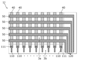
- FIG. 21 is a top view of a wiring board 1J according to the sixth embodiment.
- FIG. 21 shows a part of the periphery of the wiring board 1J. Note that the circuit element 2 is omitted in FIG.
- the first external connection terminals 110 for supplying power to the first wirings 40 and the second external connection terminals 120 for supplying power to the second wirings 50 are formed on the same wiring layer.
- a plurality of first external connection terminals 110 are formed corresponding to each of the plurality of first wirings 40 .
- a plurality of second external connection terminals 120 are formed corresponding to each of the plurality of second wirings 50 .
- the wiring board 1J has an active area 3a in which a plurality of circuit elements 2 are arranged in a matrix, and a peripheral area 3b surrounding the active area 3a. Also in this embodiment, the circuit element 2 is an LED light source and the wiring board 1J is a display device, so the active area 3a is a display area for displaying an image.
- the plurality of first external connection terminals 110 and the plurality of second external connection terminals 120 are formed in the peripheral region 3b. That is, the first external connection terminal 110 is an extraction electrode for extracting the first wiring 40 to the peripheral area 3b, and the second external connection terminal 120 is an extraction electrode for extracting the second wiring 50 to the peripheral area 3b.
- a flexible wiring board is connected as an external wiring member to each of the plurality of first external connection terminals 110 and the plurality of second external connection terminals 120 .
- the flexible wiring board for example, a COF (Chip On Film) in which a driver IC is mounted on a flexible board on which a plurality of wirings are formed can be used.
- One end of the flexible wiring board thus configured is connected to the plurality of first external connection terminals 110 or the plurality of second external connection terminals 120 by, for example, ACF (Anisotropic Conductive Film) crimping.
- Both the first external connection terminal 110 and the second external connection terminal 120 are formed in the same layer as the second wiring 50 . Specifically, both the first external connection terminal 110 and the second external connection terminal 120 are formed in the second groove portion 31 of the second insulating layer 30, which is the uppermost layer of the wiring board 1J, similarly to the second wiring 50.
- the first external connection terminal 110 connected to the first wiring 40 formed on the first insulating layer 20 is connected to the underlying first wiring 40 via the contact portion 111 formed on the first insulating layer 20.
- This contact portion 111 is an opening similar to the opening 32 formed in the second insulating layer 30, but is provided in the peripheral region 3b. That is, the opening 32 (contact portion) for connecting the first wiring 40 and the second wiring 50 is provided in the active region 3a, but the opening (contact portion 111) for connecting the first wiring 40 and the first external connection terminal 110 is provided outside the active region 3a.
- the second external connection terminal 120 connected to the second wiring 50 is part of the second wiring 50 .
- the second external connection terminal 120 is a portion where the second wiring 50 is drawn out to the peripheral region 3b.
- the first external connection terminals 110 and the second external connection terminals 120 are formed in the same wiring layer. Therefore, compared to the wiring board 1Y of Comparative Example 2 shown in FIG.
- the first external connection terminals 110Y and the second external connection terminals 120 are formed in different wiring layers. Specifically, in the wiring board 1Y of Comparative Example 2, the first external connection terminals 110Y are formed in the same layer as the first wirings 40, and the second external connection terminals 120 are formed in the same layer as the second wirings 50. Therefore, in the wiring board 1Y of Comparative Example 2, openings are formed in the first insulating layer 20 to expose the first external connection terminals 110Y.
- the second insulating layer 30 in which the first external connection terminals 110 and the second external connection terminals 120 are embedded is the uppermost layer of the wiring board 1J, so that the external wiring member such as a flexible wiring board can be easily connected to the first external connection terminals 110 or the second external connection terminals 120.
- the wiring board 1J according to the present embodiment has the same configuration as the wiring board 1 according to the first embodiment except for the configuration of the first external connection terminals 110 and the second external connection terminals.
- the first insulating layer 20 and the second insulating layer 30 are laminated above the film 10, the first wiring 40 is formed in the first groove 21 of the first insulating layer 20, and the second wiring 50 is formed in the second groove 31 and the opening 32 of the second insulating layer 30.
- the upper surface of the first wiring 40 and the lower surface of the second wiring 50 are joined together.
- the wiring substrate in Embodiments 1 to 6 above is a display device in which a plurality of LED light sources are arranged in a matrix as the circuit element 2, but the present invention is not limited to this.
- the wiring substrates in Embodiments 1 to 6 may be used for a touch panel.
- the wiring substrate can be used as a touch sensor substrate in which sensor electrodes are provided on each of the first wiring and the second wiring.
- the first external connection terminal 110 and the second external connection terminal 120 in Embodiment 6 function as extraction connection terminals for extracting the sensor signal detected by the sensor electrode to the outside.
- the third insulating layer 70 is formed above the second insulating layer 30, and in the wiring board of the fifth embodiment, the lower insulating layer 90 is formed below the first insulating layer 20.
- the present invention is not limited to this.
- another insulating layer may be formed between the first insulating layer 20 and the second insulating layer 30 .
- another insulating layer may be formed at least one place below the first insulating layer 20 , between the first insulating layer 20 and the second insulating layer 30 , and above the second insulating layer 30 .
- the technology of the present disclosure can also be used as a wiring board for electronic devices other than display devices or touch panels.
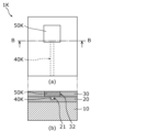
- FIG. 23(a) is a top view of the wiring board 1K
- FIG. 23(b) is a cross-sectional view taken along line BB of (a).
- the wiring board 1K includes a first wiring 40K formed in the first groove 21 of the first insulating layer 20, and a second wiring 50K formed in the opening 32 of the second insulating layer 30.
- the first wiring 40K and the second wiring 50K are joined at the opening 32.
- the first wiring 40K and the second wiring 50K function as antennas.
- FIG. 24(a) is a top view of the wiring board 1L
- FIG. 24(b) is a cross-sectional view taken along line BB of (a).
- the wiring board 1L includes a first wiring 40L formed in the first groove 21 of the first insulating layer 20 and a second wiring 50L formed in the opening 32 of the second insulating layer 30. The first wiring 40L and the second wiring 50L are joined at the opening 32.
- the first wiring 40L and the second wiring 50L function as communication lines.
- the present disclosure also includes forms obtained by applying various modifications that a person skilled in the art can come up with to the above embodiments, and forms realized by arbitrarily combining the constituent elements and functions of each embodiment within the scope of the present disclosure.
- the wiring board according to the present disclosure can be used in various electronic devices such as display devices and touch panels.
Landscapes
- Engineering & Computer Science (AREA)
- Microelectronics & Electronic Packaging (AREA)
- Manufacturing & Machinery (AREA)
- Structure Of Printed Boards (AREA)
Priority Applications (3)
| Application Number | Priority Date | Filing Date | Title |
|---|---|---|---|
| JP2023575137A JPWO2023140001A1 (https=) | 2022-01-24 | 2022-12-19 | |
| EP22922151.0A EP4472359A4 (en) | 2022-01-24 | 2022-12-19 | PRINTED CIRCUIT BOARD |
| CN202280088986.5A CN118542075A (zh) | 2022-01-24 | 2022-12-19 | 布线基板 |
Applications Claiming Priority (2)
| Application Number | Priority Date | Filing Date | Title |
|---|---|---|---|
| JP2022008416 | 2022-01-24 | ||
| JP2022-008416 | 2022-01-24 |
Publications (1)
| Publication Number | Publication Date |
|---|---|
| WO2023140001A1 true WO2023140001A1 (ja) | 2023-07-27 |
Family
ID=87348184
Family Applications (1)
| Application Number | Title | Priority Date | Filing Date |
|---|---|---|---|
| PCT/JP2022/046668 Ceased WO2023140001A1 (ja) | 2022-01-24 | 2022-12-19 | 配線基板 |
Country Status (4)
| Country | Link |
|---|---|
| EP (1) | EP4472359A4 (https=) |
| JP (1) | JPWO2023140001A1 (https=) |
| CN (1) | CN118542075A (https=) |
| WO (1) | WO2023140001A1 (https=) |
Cited By (1)
| Publication number | Priority date | Publication date | Assignee | Title |
|---|---|---|---|---|
| JP7574962B1 (ja) * | 2024-05-31 | 2024-10-29 | 大日本印刷株式会社 | 配線基板及びヘッドマウントディスプレイ |
Citations (4)
| Publication number | Priority date | Publication date | Assignee | Title |
|---|---|---|---|---|
| JP2017211826A (ja) * | 2016-05-25 | 2017-11-30 | 凸版印刷株式会社 | 配線基板、タッチパネル、カラーフィルタ基板、及び表示装置 |
| JP2019197424A (ja) * | 2018-05-10 | 2019-11-14 | シャープ株式会社 | 配線基板、表示装置及び配線基板の製造方法 |
| JP6706760B2 (ja) | 2014-09-30 | 2020-06-10 | パナソニックIpマネジメント株式会社 | タッチセンサおよび電子機器 |
| JP2021184405A (ja) * | 2020-05-21 | 2021-12-02 | パナソニックIpマネジメント株式会社 | 基板およびそれを備える表示装置 |
Family Cites Families (4)
| Publication number | Priority date | Publication date | Assignee | Title |
|---|---|---|---|---|
| JP4754850B2 (ja) * | 2004-03-26 | 2011-08-24 | パナソニック株式会社 | Led実装用モジュールの製造方法及びledモジュールの製造方法 |
| US9229260B2 (en) * | 2013-04-15 | 2016-01-05 | Eastman Kodak Company | Imprinted bi-layer micro-structure |
| US12294042B2 (en) * | 2015-03-31 | 2025-05-06 | Creeled, Inc. | Light emitting diodes and methods with encapsulation |
| CN113508033B (zh) * | 2019-03-26 | 2023-05-23 | 富士胶片株式会社 | 导电性层叠体、触摸面板、导电性层叠体的制造方法 |
-
2022
- 2022-12-19 WO PCT/JP2022/046668 patent/WO2023140001A1/ja not_active Ceased
- 2022-12-19 EP EP22922151.0A patent/EP4472359A4/en active Pending
- 2022-12-19 JP JP2023575137A patent/JPWO2023140001A1/ja active Pending
- 2022-12-19 CN CN202280088986.5A patent/CN118542075A/zh active Pending
Patent Citations (4)
| Publication number | Priority date | Publication date | Assignee | Title |
|---|---|---|---|---|
| JP6706760B2 (ja) | 2014-09-30 | 2020-06-10 | パナソニックIpマネジメント株式会社 | タッチセンサおよび電子機器 |
| JP2017211826A (ja) * | 2016-05-25 | 2017-11-30 | 凸版印刷株式会社 | 配線基板、タッチパネル、カラーフィルタ基板、及び表示装置 |
| JP2019197424A (ja) * | 2018-05-10 | 2019-11-14 | シャープ株式会社 | 配線基板、表示装置及び配線基板の製造方法 |
| JP2021184405A (ja) * | 2020-05-21 | 2021-12-02 | パナソニックIpマネジメント株式会社 | 基板およびそれを備える表示装置 |
Non-Patent Citations (1)
| Title |
|---|
| See also references of EP4472359A4 |
Cited By (1)
| Publication number | Priority date | Publication date | Assignee | Title |
|---|---|---|---|---|
| JP7574962B1 (ja) * | 2024-05-31 | 2024-10-29 | 大日本印刷株式会社 | 配線基板及びヘッドマウントディスプレイ |
Also Published As
| Publication number | Publication date |
|---|---|
| EP4472359A4 (en) | 2025-09-17 |
| JPWO2023140001A1 (https=) | 2023-07-27 |
| EP4472359A1 (en) | 2024-12-04 |
| CN118542075A (zh) | 2024-08-23 |
Similar Documents
| Publication | Publication Date | Title |
|---|---|---|
| CN212209306U (zh) | 按键背光光源装置及背光键盘 | |
| US20200154564A1 (en) | Light-emitting module | |
| CN111048566B (zh) | 一种有机发光显示面板及显示装置 | |
| US11538972B2 (en) | Light-emitting unit and manufacturing method of light-emitting unit | |
| CN114114762B (zh) | 显示基板及其制作方法、显示装置 | |
| KR20190044016A (ko) | 표시 장치 및 표시 장치 제조 방법 | |
| WO2017115712A1 (ja) | 発光モジュール | |
| US11310920B2 (en) | Circuit board, method for manufacturing the same, and backlight | |
| TWI868324B (zh) | 發光顯示裝置及其製造方法 | |
| CN111863857B (zh) | Led显示基板及其制备方法显示面板 | |
| US12057538B2 (en) | Driving substrate and method for manufacturing the same, light-emitting substrate and display device | |
| WO2023140001A1 (ja) | 配線基板 | |
| CN113506810B (zh) | 面板装置及面板装置的制造方法 | |
| CN114375502B (zh) | Led模组 | |
| CN111162157A (zh) | 一种led显示模组 | |
| KR102583731B1 (ko) | 협-베젤 전계 발광 조명장치 | |
| CN114512522B (zh) | 显示面板和显示装置 | |
| CN102136431A (zh) | 发光二极管封装及其制作方法 | |
| US12568726B2 (en) | Electronic device having light-emitting diode display modules configured for reducing gap sizes at splices of modules | |
| CN112350065A (zh) | 显示面板、显示装置和显示面板的制作方法 | |
| JP2021057465A (ja) | 発光装置の製造方法 | |
| KR102911563B1 (ko) | 표시 패널 및 표시 장치 | |
| JP2007287503A (ja) | 有機elディスプレイ | |
| CN110752109B (zh) | 背光模块及其背光模块制造方法 | |
| WO2024111282A1 (ja) | 多層配線基板 |
Legal Events
| Date | Code | Title | Description |
|---|---|---|---|
| 121 | Ep: the epo has been informed by wipo that ep was designated in this application |
Ref document number: 22922151 Country of ref document: EP Kind code of ref document: A1 |
|
| ENP | Entry into the national phase |
Ref document number: 2023575137 Country of ref document: JP Kind code of ref document: A |
|
| WWE | Wipo information: entry into national phase |
Ref document number: 18728159 Country of ref document: US |
|
| WWE | Wipo information: entry into national phase |
Ref document number: 202280088986.5 Country of ref document: CN |
|
| NENP | Non-entry into the national phase |
Ref country code: DE |
|
| ENP | Entry into the national phase |
Ref document number: 2022922151 Country of ref document: EP Effective date: 20240826 |