WO2023139670A1 - 電極チップ整形治具及び電極チップ整形装置 - Google Patents
電極チップ整形治具及び電極チップ整形装置 Download PDFInfo
- Publication number
- WO2023139670A1 WO2023139670A1 PCT/JP2022/001691 JP2022001691W WO2023139670A1 WO 2023139670 A1 WO2023139670 A1 WO 2023139670A1 JP 2022001691 W JP2022001691 W JP 2022001691W WO 2023139670 A1 WO2023139670 A1 WO 2023139670A1
- Authority
- WO
- WIPO (PCT)
- Prior art keywords
- shaping
- tip
- electrode tip
- electrode
- distal end
- Prior art date
- Legal status (The legal status is an assumption and is not a legal conclusion. Google has not performed a legal analysis and makes no representation as to the accuracy of the status listed.)
- Ceased
Links
Images






Classifications
-
- B—PERFORMING OPERATIONS; TRANSPORTING
- B23—MACHINE TOOLS; METAL-WORKING NOT OTHERWISE PROVIDED FOR
- B23K—SOLDERING OR UNSOLDERING; WELDING; CLADDING OR PLATING BY SOLDERING OR WELDING; CUTTING BY APPLYING HEAT LOCALLY, e.g. FLAME CUTTING; WORKING BY LASER BEAM
- B23K11/00—Resistance welding; Severing by resistance heating
- B23K11/10—Spot welding; Stitch welding
- B23K11/11—Spot welding
-
- B—PERFORMING OPERATIONS; TRANSPORTING
- B23—MACHINE TOOLS; METAL-WORKING NOT OTHERWISE PROVIDED FOR
- B23K—SOLDERING OR UNSOLDERING; WELDING; CLADDING OR PLATING BY SOLDERING OR WELDING; CUTTING BY APPLYING HEAT LOCALLY, e.g. FLAME CUTTING; WORKING BY LASER BEAM
- B23K11/00—Resistance welding; Severing by resistance heating
- B23K11/30—Features relating to electrodes
Definitions
- the present invention provides an electrode tip shaping jig and an electrode tip shaping apparatus for shaping and regenerating an electrode tip that has been swollen and deformed by electric resistance welding into a regular shape. More specifically, the extension of the tip of the electrode tip along the outer peripheral surface of the electrode tip from the base end side of the electrode tip (hereinafter referred to as a scarf piece) is prevented from being formed in the radial direction, and the alloy layer formed on the tip surface is formed to a predetermined thickness.
- the present invention relates to an electrode tip shaping jig and an electrode tip shaping device for shaping the electrode tip into a regular shape while leaving the electrode tip with a .
- the term “shaping” means shaping the deformed portion into a regular shape by stretching it, unlike the concept of polishing and shaping the bulging deformed portion of the electrode tip into a regular shape by grinding or cutting.
- the "regular shape” originally means the shape of the electrode tip when not in use, but the electrode tip shaped in the present invention has a slightly shorter length in the axial direction and an alloy layer with a predetermined layer thickness remains on the tip surface, and the shape does not completely match the shape of the unused electrode tip.
- the tip of the electrode tip bulges (increases in diameter) and wears due to pressure contact with the workpiece, and the metal of the base material of the tip evaporates and wears due to sputtering.
- an alloy layer of copper which is the base material of the electrode tip, and the work material or its plating material is formed on the front end face of the electrode tip.
- the alloy layer has a higher electrical resistance than the copper or copper alloy that is the base material of the electrode tip, and the welding current cannot be effectively applied to the work to form a high-quality weld nugget for welding, resulting in a problem of poor welding quality.
- the bulging deformed portion of the electrode tip is polished (cut) by an electrode polishing machine to restore the normal shape.
- the present applicant proposed an electrode tip shaping jig disclosed in Patent Document 1 in order to solve the above-described drawbacks of the conventional electrode tip polishing apparatus.
- the electrode tip shaping jig rotates as an electric motor is driven, and presses the respective outer peripheral surface forming projections against the outer peripheral surface of the tip of the electrode tip to press and stretch the bulging deformed portion to shape it into a regular shape.
- part of the distal end portion is pushed out around the outer periphery on the opposite side (base end side of the electrode tip) by the outer peripheral surface forming protrusion that presses against the outer peripheral surface of the distal end portion of the electrode tip, generating a scarf piece that becomes rotational resistance and causes a problem that the shaping work cannot be performed efficiently.
- the scarf piece when the scarf piece is formed, the scarf piece acts as a rotational resistance, and the shaping work cannot be performed efficiently. Therefore, it is necessary to interrupt the shaping work to cut off and remove the scarf.
- weld nugget in order to form a good quality weld nugget between the works, it is desirable to form the weld nugget so as to extend from the outer peripheral part to the central part by increasing the current applied to the outer peripheral side with respect to the current applied to the central part of the tip surface of the electrode tip at the initial stage of current application.
- the problem to be solved is that the conventional shaping jig presses one shaping protrusion to the entire outer peripheral surface of the distal end portion, so that the rotation resistance of the electrode tip shaping jig increases and the shaping work cannot be performed efficiently.
- a scarf piece is formed as a residual portion of the straightening, which acts as a rotational resistance, and the electrode tip cannot be efficiently regenerated.
- the shaping work must be interrupted in order to cut off and remove the formed scarf piece, resulting in poor shaping work efficiency.
- the electrode tip shaping jig according to claim 1 comprises: a shaping chamber having a recessed cup-shaped inner peripheral surface into which a tip end of an electrode tip can be inserted; a notch portion in which the outer peripheral side of the shaping chamber is notched except for a partial bottom surface of the shaping chamber; A tip surface shaping portion, which extends in a radial direction and is pressed against the tip surface of the electrode tip and scrapes off a part of the alloy layer formed on the tip surface, shaping the tip surface shaping region on the tip surface into a planar shape, a curved surface shape, or a combination thereof; When the tip surface of the electrode tip reaches the bottom surface of the shaping chamber, the alloy layer generated on the tip surface is scraped off so that the alloy layer remains with a required layer thickness, and the tip surface is flattened, curved, or combined.
- the most important feature is that the electrode tip is shaped into a regular shape by cutting the excessively stretched portion.
- An electrode tip shaping apparatus comprising: a rotary disc provided with a boss detachably mounted in a state where the electrode tip shaping jig according to any one of claims 1 to 5 is detachably attached at the center thereof; a holder for rotatably supporting the rotary disc; an electric motor connected to the rotary disc for rotating the rotary disc; An electrode tip whose tip portion is deformed by electric resistance welding and an alloy layer is formed on the tip surface is inserted, and the corresponding shaping portions are pressed against each of the assumed shaping regions on at least the tip side and the base end side of the tip portion of the electrode tip, and the corresponding shaping portions are pressed and stretched and shaped in the respective directions of the proximal side and the tip side.
- the most important feature of the electrode tip is that the electrode tip is shaped into a regular shape by cutting the outer periphery of the tip with a cutting blade that presses against the outer periphery of the tip by pressing and extending the tip face into one of a flat surface, a curved surface, and a combination of these while scraping off the electrode tip.
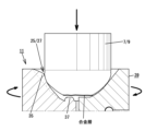
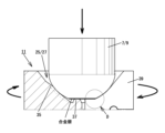
- the corresponding shaping sections are pressed in sequence and stretched and shaped in the respective directions of the proximal side and the distal side, and when the distal surface of the electrode tip reaches the bottom of the shaping chamber, the alloy layer generated on the distal surface by the distal surface shaping section that presses against the distal surface is scraped off so that the alloy layer remains with a required layer thickness.
- the most important feature is that the electrode tip is shaped into a regular shape by cutting the outer periphery of the distal end with a cutting blade that presses against the outer periphery.
- the present invention by providing a plurality of shaping sections corresponding to a plurality of expected shaping areas on the outer peripheral surface of the distal end portion of the electrode tip, it is possible to efficiently perform shaping work while avoiding an increase in rotational resistance.
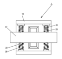
- FIG. 1 It is a partially exploded perspective view showing an outline of an electrode tip shaping device. 1. It is the front view which looked at the electrode tip reproduction
- Each of the electrode tips 7 and 9 is formed with a boss that can be inserted into an attachment shaft (not shown) provided on the attachment arm, and is made of copper (Cu), copper-chromium alloy (Cr-Cu), or the like, which has low electrical resistance and is easily plastically deformable. shown).
- chip discharge holes 31 extending in the axial direction of the electrode tip shaping jig 11 and penetrating through the partition between them.
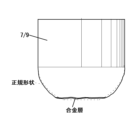
- the solid line indicates a state in which the tip end portions of the electrode tips 7 and 9 are crushed to have a large diameter or is partially worn, and the normal shape is indicated by a dashed line.
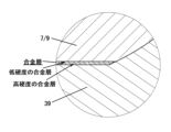
- an alloy layer with low hardness (BCr-Zn layer) and an alloy layer with high hardness (YCr-Zn layer, Fe-Zn layer) are formed from the tip surface side.
- the shaping action by the first and second shaping sections 33 and 35 has been described separately for convenience of explanation, but in reality, the shaping work is performed by acting in a complex manner at the boundaries of the regions of the distal end portions of the electrode tips 7 and 9.
- the welding current applied to the work via the electrode tips 7 and 9 has a current distribution such that a large current flows outside the tip surface shaping region c where the alloy layer remains.
- the workpiece is first heated at a location corresponding to the outer peripheral side of the tip surface, and then is heated and melted from a location corresponding to the tip surface shaping region c, that is, from the outside toward the center, and a uniform high-quality weld nugget in a uniform heating state and size is formed and welded.
- the shaping regions are assumed to be formed on the distal end side and the proximal end side of the distal end portions of the electrode tips 7 and 9, respectively, and the corresponding shaping portions are provided respectively.
- Electrode tip regeneration device 7/9 Electrode tip 11 Electrode tip shaping jig 13 Rotating plate 15 Fixed plate 17 Holder 18 Electric motor 19 Main body 21 Guide shaft 23 Compression spring 25/27 Shaping chamber 29 Notch 29a Notch surface 29b Locking recess 29c Screw hole 31 Chip discharge hole 33 First shaping part 35 Second shaping part 37 Tip face shaping part 39 Cutting blade 3 9a Blade portion 39b Locked portion 39c Through hole 39d Screw
Landscapes
- Engineering & Computer Science (AREA)
- Mechanical Engineering (AREA)
- Resistance Welding (AREA)
Priority Applications (2)
| Application Number | Priority Date | Filing Date | Title |
|---|---|---|---|
| PCT/JP2022/001691 WO2023139670A1 (ja) | 2022-01-19 | 2022-01-19 | 電極チップ整形治具及び電極チップ整形装置 |
| JP2022506824A JP7121962B1 (ja) | 2022-01-19 | 2022-01-19 | 電極チップ整形治具及び電極チップ整形装置 |
Applications Claiming Priority (1)
| Application Number | Priority Date | Filing Date | Title |
|---|---|---|---|
| PCT/JP2022/001691 WO2023139670A1 (ja) | 2022-01-19 | 2022-01-19 | 電極チップ整形治具及び電極チップ整形装置 |
Publications (1)
| Publication Number | Publication Date |
|---|---|
| WO2023139670A1 true WO2023139670A1 (ja) | 2023-07-27 |
Family
ID=82929877
Family Applications (1)
| Application Number | Title | Priority Date | Filing Date |
|---|---|---|---|
| PCT/JP2022/001691 Ceased WO2023139670A1 (ja) | 2022-01-19 | 2022-01-19 | 電極チップ整形治具及び電極チップ整形装置 |
Country Status (2)
| Country | Link |
|---|---|
| JP (1) | JP7121962B1 (https=) |
| WO (1) | WO2023139670A1 (https=) |
Families Citing this family (1)
| Publication number | Priority date | Publication date | Assignee | Title |
|---|---|---|---|---|
| JP7219935B1 (ja) * | 2022-09-09 | 2023-02-09 | 有限会社Tne | 電極チップ再生装置 |
Citations (4)
| Publication number | Priority date | Publication date | Assignee | Title |
|---|---|---|---|---|
| JP2009136882A (ja) * | 2007-12-03 | 2009-06-25 | Nadex Co Ltd | 電極チップ整形装置 |
| DE102012008257A1 (de) * | 2012-04-25 | 2013-10-31 | Peter Lutz | Fräskopf für das Entfernen von Ablagerungen an Schweißelektroden für das Widerstandsschweißen |
| JP2015058446A (ja) * | 2013-09-18 | 2015-03-30 | トヨタ車体株式会社 | スポット溶接用チップの整形方法 |
| JP2017213590A (ja) * | 2016-06-02 | 2017-12-07 | 有限会社Tne | 電極チップ再生具及び電極チップ再生装置 |
Family Cites Families (2)
| Publication number | Priority date | Publication date | Assignee | Title |
|---|---|---|---|---|
| JP4399435B2 (ja) * | 2005-09-01 | 2010-01-13 | 株式会社キョクトー | チップ成形機 |
| JP5962553B2 (ja) * | 2013-03-12 | 2016-08-03 | トヨタ車体株式会社 | スポット溶接用チップの整形装置 |
-
2022
- 2022-01-19 WO PCT/JP2022/001691 patent/WO2023139670A1/ja not_active Ceased
- 2022-01-19 JP JP2022506824A patent/JP7121962B1/ja active Active
Patent Citations (4)
| Publication number | Priority date | Publication date | Assignee | Title |
|---|---|---|---|---|
| JP2009136882A (ja) * | 2007-12-03 | 2009-06-25 | Nadex Co Ltd | 電極チップ整形装置 |
| DE102012008257A1 (de) * | 2012-04-25 | 2013-10-31 | Peter Lutz | Fräskopf für das Entfernen von Ablagerungen an Schweißelektroden für das Widerstandsschweißen |
| JP2015058446A (ja) * | 2013-09-18 | 2015-03-30 | トヨタ車体株式会社 | スポット溶接用チップの整形方法 |
| JP2017213590A (ja) * | 2016-06-02 | 2017-12-07 | 有限会社Tne | 電極チップ再生具及び電極チップ再生装置 |
Also Published As
| Publication number | Publication date |
|---|---|
| JP7121962B1 (ja) | 2022-08-19 |
| JPWO2023139670A1 (https=) | 2023-07-27 |
Similar Documents
| Publication | Publication Date | Title |
|---|---|---|
| US9346118B2 (en) | Forming and re-forming welding electrodes with contoured faces | |
| EP1005942B1 (en) | Welding electrode reshaping device | |
| US4610153A (en) | Method and apparatus for dressing spot welding tips | |
| WO2023139670A1 (ja) | 電極チップ整形治具及び電極チップ整形装置 | |
| JP6489703B2 (ja) | 電極チップ再生具及び電極チップ再生装置 | |
| US8449231B2 (en) | Milling cutter for dressing resistance welding electrodes | |
| JP3879533B2 (ja) | 切削刃およびチップドレッサー | |
| CN100528450C (zh) | 电极头整形装置以及电极头整形工具 | |
| CN213104529U (zh) | 一种焊接电极的修磨刀片 | |
| JP7219935B1 (ja) | 電極チップ再生装置 | |
| US20210213559A1 (en) | Electrode re-conditioning tool and method of using the same | |
| JP2014151327A (ja) | 電極チップ再生具及び電極チップ再生方法 | |
| JP5131924B2 (ja) | 電極チップ再生具 | |
| JP2010029883A (ja) | 溶接用電極チップの整形装置およびその整形方法 | |
| CN101134249A (zh) | 硬质合金精加工指形铣刀及加工工艺方法 | |
| JP2013013939A (ja) | 電極チップ再生工具及びその再生方法 | |
| JP5170613B2 (ja) | 電極チップ再生工具及びその再生方法 | |
| JP5811324B2 (ja) | 溶接用の電極チップの整形工具、およびその整形装置 | |
| JP2011240376A (ja) | 電極研磨装置 | |
| JP7541421B2 (ja) | 電極チップの切削再生方法及びチップドレス用切削カッター | |
| US20230390857A1 (en) | Electrode dressing system for spot welding press-hardened steels | |
| JP2025163323A (ja) | 電気抵抗溶接方法 | |
| JP2000351082A (ja) | 電極チップドレス装置 | |
| JPH09239562A (ja) | 電極チップドレッサ用のカッター | |
| JP2025094596A (ja) | 抵抗溶接方法 |
Legal Events
| Date | Code | Title | Description |
|---|---|---|---|
| WWE | Wipo information: entry into national phase |
Ref document number: 2022506824 Country of ref document: JP |
|
| 121 | Ep: the epo has been informed by wipo that ep was designated in this application |
Ref document number: 22921831 Country of ref document: EP Kind code of ref document: A1 |
|
| NENP | Non-entry into the national phase |
Ref country code: DE |
|
| 122 | Ep: pct application non-entry in european phase |
Ref document number: 22921831 Country of ref document: EP Kind code of ref document: A1 |