WO2023136235A1 - パッケージ - Google Patents
パッケージ Download PDFInfo
- Publication number
- WO2023136235A1 WO2023136235A1 PCT/JP2023/000273 JP2023000273W WO2023136235A1 WO 2023136235 A1 WO2023136235 A1 WO 2023136235A1 JP 2023000273 W JP2023000273 W JP 2023000273W WO 2023136235 A1 WO2023136235 A1 WO 2023136235A1
- Authority
- WO
- WIPO (PCT)
- Prior art keywords
- optical
- chips
- chip
- substrate
- package
- Prior art date
- Legal status (The legal status is an assumption and is not a legal conclusion. Google has not performed a legal analysis and makes no representation as to the accuracy of the status listed.)
- Ceased
Links
Images





Classifications
-
- H—ELECTRICITY
- H01—ELECTRIC ELEMENTS
- H01S—DEVICES USING THE PROCESS OF LIGHT AMPLIFICATION BY STIMULATED EMISSION OF RADIATION [LASER] TO AMPLIFY OR GENERATE LIGHT; DEVICES USING STIMULATED EMISSION OF ELECTROMAGNETIC RADIATION IN WAVE RANGES OTHER THAN OPTICAL
- H01S5/00—Semiconductor lasers
- H01S5/02—Structural details or components not essential to laser action
- H01S5/024—Arrangements for thermal management
-
- H—ELECTRICITY
- H10—SEMICONDUCTOR DEVICES; ELECTRIC SOLID-STATE DEVICES NOT OTHERWISE PROVIDED FOR
- H10F—INORGANIC SEMICONDUCTOR DEVICES SENSITIVE TO INFRARED RADIATION, LIGHT, ELECTROMAGNETIC RADIATION OF SHORTER WAVELENGTH OR CORPUSCULAR RADIATION
- H10F77/00—Constructional details of devices covered by this subclass
-
- H—ELECTRICITY
- H10—SEMICONDUCTOR DEVICES; ELECTRIC SOLID-STATE DEVICES NOT OTHERWISE PROVIDED FOR
- H10W—GENERIC PACKAGES, INTERCONNECTIONS, CONNECTORS OR OTHER CONSTRUCTIONAL DETAILS OF DEVICES COVERED BY CLASS H10
- H10W76/00—Containers; Fillings or auxiliary members therefor; Seals
- H10W76/10—Containers or parts thereof
Definitions
- This technology is related to packaging. Specifically, the present technology relates to a package capable of mounting multiple chips.
- multiple optical chips mounted on a package are sometimes installed so as to satisfy relative positional relationships. For example, two side portions of the ceramic package are brought into contact with two contact portions of a manufacturing jig, respectively, and a plurality of light emitting/receiving elements are installed in predetermined regions of the ceramic package based on the contact portions of the manufacturing jig. A method for doing so has been proposed (see, for example, Patent Document 1).
- This technology was created in view of this situation, and aims to make it possible to design the heat dissipation properties of multiple chips mounted in a single package separately.
- the present technology has been made to solve the above-described problems.
- the package comprises a plurality of heat dissipating members respectively provided at positions where the openings are closed, and a plurality of chips mounted on the plurality of heat dissipating members, at least a part of which is located in each of the openings. This brings about an effect that the heat dissipation properties of the plurality of chips are individually set while aligning the reference surfaces of the plurality of chips.
- the material of the heat dissipation member may be metal or resin mixed with filler. This brings about an effect that the thermal conductivity of the heat radiating member is higher than that of the substrate.
- the heat dissipation member may have a coefficient of thermal expansion closer to that of the chip than that of the substrate.
- At least one of the plurality of heat dissipating members may differ from other heat dissipating members in at least one of plate thickness and material.
- a Peltier element may be provided between at least one of the plurality of chips and a heat dissipation member on which the chip is mounted. This provides an effect of cooling the chip according to the chip type.
- the first side surface may further include a heat sink provided on the back surface side of at least one of the plurality of heat radiating members. This brings about an effect that the heat dissipation of the chip is improved according to the type of the chip.
- the first side surface may further include a connector provided upright on the back surface of the substrate. This brings about the effect that the package is electrically connected without increasing the installation area of the package.
- the chip may include an optical chip on which an optical element is formed. This brings about an effect that the heat dissipation properties of the plurality of optical chips are individually set while aligning the optical reference planes of the plurality of optical chips.
- At least one of the plurality of optical chips may be of a different type from the other optical chips. This brings about the effect of providing multiple optical functions while using a single package.
- the first side surface it may further include a lens that converges light onto the optical chip, and a housing that is fastened to the substrate and supports the lens on the optical chip. This brings about the effect that the lens and the optical chip are integrated.
- the second side surface includes a substrate provided with a plurality of openings, a plurality of chips at least partially positioned within the openings, and the plurality of chips mounted separately from the substrate. and a heat radiating member having a high thermal conductivity, having gaps between respective mounting regions of the plurality of chips, and provided at a position where the plurality of openings are blocked.
- the material of the heat dissipation member may be metal or resin mixed with filler. This brings about an effect that the thermal conductivity of the heat radiating member is higher than that of the substrate.
- the heat dissipation member may have a coefficient of thermal expansion closer to that of the chip than that of the substrate.
- the plate thickness of the heat radiating member may be different at at least one position of the plurality of openings from the plate thickness of the heat radiating member at other positions of the openings.
- the device may further include a Peltier element provided between at least one of the plurality of chips and a heat dissipation member at the mounting position of the chip. This provides an effect of cooling the chip according to the chip type.
- a heat sink may be provided on the rear surface side of the heat dissipation member in at least one position of the plurality of openings. This brings about an effect that the heat dissipation of the chip is improved according to the type of the chip.
- the second side surface may further include a connector provided upright on the back surface of the substrate. This brings about the effect that the package is electrically connected without increasing the installation area of the package.
- the chip may include an optical chip on which an optical element is formed. This brings about an effect that the heat dissipation properties of the plurality of optical chips are individually set while aligning the optical reference planes of the plurality of optical chips.
- At least one of the plurality of optical chips may be of a different type from the other optical chips. This brings about the effect of providing multiple optical functions while using a single package.
- a lens that collects light onto the optical chip and a housing that is fastened to the substrate and supports the lens on the optical chip may be further provided. This brings about the effect that the lens and the optical chip are integrated.
- the heat dissipation member may be a plate material. This brings about an effect of facilitating mounting while suppressing an increase in the cost of the heat radiating member.
- the heat dissipation member may be a metal plate. This brings about the effect of improving the heat dissipation of a plurality of chips while suppressing an increase in the cost of the heat dissipation member.
- the heat dissipation member may have a step at a position surrounding the mounting area of the chip. This brings about the effect that the height position of the chip from the optical reference plane can be adjusted.
- the height of the steps may be set so that the heights of the plurality of chips are the same when the back surface of the substrate is used as an optical reference plane. This brings about the effect of facilitating the positioning of a plurality of chips.
- At least one of the plurality of chips may have a different chip thickness from other chips. This brings about an effect that chips of different types can be mounted.
- the back surface of the heat dissipation member may be flat. This brings about the effect of facilitating the attachment of the heat sink to the heat radiating member.
- the semiconductor device further comprises: a plurality of cover members respectively covering the plurality of chips; and a plurality of spacers provided on the substrate and supporting the plurality of cover members respectively on the chips. good too. This brings about the effect of ensuring the sealing performance of a plurality of chips.
- At least one of the plurality of spacers may differ from other spacers in material or height. This brings about the effect of optimizing the sealing performance according to the type of chip.
- the substrate may have a step at a position surrounding the supporting surface of the spacer. This brings about an effect that the height position of the cover member is changed according to the chip thickness.
- FIG. 1 is a diagram showing a configuration example of a package according to a first embodiment
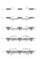
- FIG. 4A to 4C are cross-sectional views showing an example of a method for manufacturing the package according to the first embodiment
- FIG. 11 is a cross-sectional view showing a configuration example of a package according to a second embodiment
- FIG. 11 is a cross-sectional view showing a configuration example of a package according to a third embodiment
- FIG. 11 is a cross-sectional view showing a configuration example of a package according to a fourth embodiment
- FIG. 11 is a cross-sectional view showing a configuration example of a package according to a fifth embodiment
- FIG. 11 is a cross-sectional view showing a configuration example of a package according to a sixth embodiment
- FIG. 21 is a diagram illustrating a configuration example of a package according to a seventh embodiment
- FIG. FIG. 21 is a diagram illustrating a configuration example of a package according to an eighth embodiment
- FIG. FIG. 21 is a cross-sectional view showing a configuration example of a package according to a ninth embodiment
- FIG. 21 is a cross-sectional view showing a configuration example of a package according to a tenth embodiment
- FIG. 21 is a cross-sectional view showing a configuration example of a package according to an eleventh embodiment
- FIG. 21 is a cross-sectional view showing a configuration example of a package according to a twelfth embodiment
- FIG. 21 is a cross-sectional view showing a configuration example of a package according to a thirteenth embodiment
- FIG. 21 is a diagram showing a configuration example of a package according to a fourteenth embodiment
- First Embodiment Example in which a plurality of optical chips are individually mounted on a plurality of heat sinks provided in a single package
- Second Embodiment Example in which a plurality of heat sinks provided in a single package have mutually different plate thicknesses
- Third Embodiment Example of providing a common lens for a plurality of optical chips mounted in a single package
- Fourth embodiment an example in which a lens is individually provided for each of a plurality of optical chips mounted in a single package
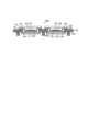
- FIG. 1 is a diagram showing a configuration example of a package according to the first embodiment.
- a is a cross-sectional view showing a configuration example of the package 100 cut in the vertical direction
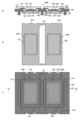
- b is a plan view showing a configuration example of the heat sinks 111 and 112
- c is the package 100.
- 1 is a plan view showing a configuration example of FIG. A in the same figure is cut along the A1-A2 line of c in the same figure.
- the package 100 includes a substrate 101 and heat sinks 111 and 112 .
- Substrate 101 is provided with a plurality of openings 181 and 182 .
- Radiator plates 111 and 112 are provided on the back side of substrate 101 at positions where openings 181 and 182 are blocked.
- An optical chip 121 is mounted on the heat sink 111 and an optical chip 122 is mounted on the heat sink 112 . At this time, at least portions of the optical chips 121 and 122 are positioned within the openings 181 and 182, respectively.
- the periphery of optical chips 121 and 122 may be surrounded by openings 181 and 182, respectively.
- solder may be used, metal paste may be used, or diffusion bonding using a metal such as Cu may be used.
- Components other than the optical chips 121 and 122 may be mounted on the heat sinks 111 and 112, respectively. At this time, the back surface of the substrate 101 can be used as an optical reference plane for the optical chips 121 and 122 .
- the optical device may be a solid-state imaging device such as a CCD (Charged Coupled Device) or CMOS (Complementary Metal-Oxide Semiconductor).
- the light received by the solid-state imaging device may be visible light, near-infrared light (NIR: Near InfraRed), short-wave infrared light (SWIR: Short Wavelength InfraRed), ultraviolet light, X-rays, or the like.
- NIR Near InfraRed
- SWIR Short Wavelength InfraRed
- the optical element may be a light receiving element such as PD (Photo Diode), or a light emitting element such as LD (Laser Diode), LED (Light Emitting Diode) or VCSEL (Vertical Cavity Surface Emitting Laser).
- the optical elements may be MEMS (Micro Electro Mechanical Systems) elements such as optical switches and mirror devices.
- the optical elements formed on the optical chips 121 and 122 may be of the same type, or may be of different types. Examples of different types of optical elements formed on the optical chips 121 and 122 include, for example, a solid-state imaging device in which the optical element formed in the optical chip 121 is sensitive to visible light, and an optical element formed in the optical chip 122. may be a solid-state imaging device sensitive to near-infrared light.
- the material used for the base material of the optical chips 121 and 122 may be a semiconductor such as Si, GaAs or InGaAsP, or a dielectric such as LiNbO 3 , glass or transparent resin.
- a Si substrate is used for the optical chip 121
- a solid-state imaging device sensitive to near-infrared light is formed on the optical chip 122.
- An InGaAs substrate can be used for the chip 122 .
- the substrate 101 for example, an organic substrate or a ceramic substrate can be used. Wiring and pad electrodes can be formed on the substrate 101 .
- the substrate 101 may be an interposer substrate, a printed substrate, or a buildup substrate. Also, a terminal electrically connected to the connector 102 may be formed on the substrate 101 .
- the width W1 of each of the heat sinks 111 and 112 can be made equal to the width W2 of the substrate 101. At this time, the widthwise end positions of the heat sinks 111 and 112 and the widthwise end position of the substrate 101 can be aligned with each other.
- the radiator plates 111 and 112 can be attached to the back side of the substrate 101 via an adhesive, for example.
- an adhesive for example, insulating resin such as epoxy resin can be used.
- Heat sinks 111 and 112 can be made of a material with higher thermal conductivity than substrate 101 . Moreover, it is preferable that the thermal expansion coefficients of the heat sinks 111 and 112 be closer to those of the optical chips 121 and 122 than that of the substrate 101 .
- the thermal expansion coefficient may be a linear expansion coefficient or a volume expansion coefficient.
- the material of heat sinks 111 and 112 may be metal or resin mixed with filler. Depending on the types of optical chips 121 and 122, the materials of heat sinks 111 and 112 may be different from each other. For example, if Si substrates are used for the optical chips 121 and 122, CuW or Invar can be used as the metal forming the radiator plates 111 and 112. FIG. Alternatively, CFRP (Carbon Fiber Reinforced Plastics) can be used as the filler-mixed resin.
- the thermal expansion coefficients of the heat sinks 111 and 112 can be adjusted to those of the optical chips 121 and 122 by adjusting the content of carbon fiber mixed in CFRP.
- the coefficient of thermal expansion can be approximated.
- the heat sinks 111 and 112 are examples of the heat sink members described in the claims.
- a connector 102 is provided on the back side of the substrate 101 .
- Connector 102 may be positioned between heat sinks 111 and 112 or adjacent to each heat sink 111 and 112 .
- the connector 102 can be fixed to the substrate 101 upright on the back surface of the substrate 101 .
- the connector 102 may be adhered to the back surface of the substrate 101 via an adhesive.
- the terminals of connector 102 may be electrically connected to substrate 101, for example, based on soldering.
- the height of the connector 102 in the normal direction from the back surface of the substrate 101 can be higher than the height of the heat sinks 111 and 112 in the normal direction from the back surface of the substrate 101 .
- a projecting electrode such as a bump electrode or a pillar electrode may be used instead of the connector 102 .
- each of the optical chips 121 and 122 has color filters 131 and 132 and on-chip lenses 141 and 142 as indicated by a in FIG. may be provided for each pixel.
- Each of the color filters 131 and 132 may form, for example, a Bayer array.
- Each optical chip 121 and 122 is electrically connected to the substrate 101 via bonding wires 151 and 152, respectively.
- the material of the bonding wires 151 and 152 may be Au or Al, for example.
- a cover glass 171 and 172 is provided on each optical chip 121 and 122 .
- Each cover glass 171 and 172 can be supported on substrate 101 via spacers 161 and 162 .
- Materials for the cover glasses 171 and 172 may be different from each other according to the types of the optical chips 121 and 122 .
- the cover Quartz may be used as the material of the glass 172 .
- Resin for example, can be used as the material of each spacer 161 and 162 .
- a filler may be mixed into the resin to increase the strength of each spacer 161 and 162 .
- the height of each spacer 161 and 162 can be set so that cover glasses 171 and 172 do not contact bonding wires 151 and 152 .
- insulating resin such as epoxy resin can be used for bonding the cover glasses 171 and 172 to the spacers 161 and 162 and bonding the spacers 161 and 162 to the substrate 101.
- insulating resin such as epoxy resin can be used for bonding the cover glasses 171 and 172 to the spacers 161 and 162 and bonding the spacers 161 and 162 to the substrate 101 .
- each cover glass 171 and 172 may be removable from the substrate 101 .
- a pressure-sensitive adhesive whose adhesive force is rapidly reduced by ultraviolet irradiation may be used for adhesion between the cover glasses 171 and 172 and the spacers 161
- the heat sinks 111 and 112 and the substrate 101 are provided with fastening holes 191 to 193, respectively.
- the fastening holes 191 to 193 can be provided at both ends in the width direction of each of the radiator plates 111 and 112 and the substrate 101 .
- Fastening holes 191 to 193 can be used to fasten a lens-supporting housing to the substrate 101 .
- optical chips 121 and 122 are CMOS image sensors.
- Such optical chips 121 and 122 can be used, for example, in fields such as appreciation, transportation, home appliances, medicine, healthcare, security, beauty, sports, and agriculture.
- the optical chips 121 and 122 can be applied to devices that take images for viewing, such as digital cameras, smart phones, and mobile phones with camera functions. can.
- the optical chips 121 and 122 are used as in-vehicle sensors that capture images of the front, rear, surroundings, and interior of a vehicle for safe driving such as automatic stopping, recognition of the driver's state, and the like. It can be applied to a device that captures an image for use in transportation. Alternatively, in the field of transportation, the optical chips 121 and 122 may be applied to devices used for transportation, such as surveillance cameras that monitor running vehicles and roads, and ranging sensors that measure distances between vehicles. good.
- the optical chips 121 and 122 are devices provided in home appliances such as television receivers, refrigerators, and air conditioners, for example, to capture user gestures and operate devices according to the gestures. can be applied to
- the optical chips 121 and 122 can be applied to medical and health care devices such as endoscopes and devices for imaging blood vessels by receiving infrared light. can.
- the optical chips 121 and 122 can be applied, for example, to security devices such as surveillance cameras for crime prevention and cameras for person authentication.
- the optical chips 121 and 122 can be applied, for example, to devices used for beauty care, such as skin measuring instruments that take images of the skin and microscopes that take images of the scalp.
- the optical chips 121 and 122 can be applied, for example, to devices used for sports such as action cameras and wearable cameras for sports.
- the optical chips 121 and 122 can be applied to devices used for agriculture, such as cameras for monitoring the conditions of fields and crops, and the conditions of livestock. can.
- optical chips 121 and 122 monitor the entry and exit of people into a building, for example, to turn lights on and off or open and close blinds in response to people entering and leaving the building. It can be applied to a device used for illumination and daylighting such as a camera that does the work.
- the optical chips 121 and 122 are used in the manufacturing industry, for example, as cameras for monitoring the status of products, intermediates or parts on the manufacturing line, or for checking the position of robot arms and the like. It can be applied to the equipment provided.
- the optical chips 121 and 122 can be applied to devices used in the steel and chemical industries, such as cameras that monitor the temperature, color, and state of reacting substances. .
- FIG. 2 is a cross-sectional view showing an example of the method of manufacturing the package according to the first embodiment.
- a plurality of openings 181 and 182 are formed in the substrate 101 as shown in a in the figure. At this time, wirings, electrodes, and the like may be formed on the substrate 101 in regions other than the positions of the openings 181 and 182 .
- the openings 181 and 182 may be formed by, for example, punching the substrate 101 or cutting the substrate 101 along the contours of the openings 181 and 182 using a blade or laser.
- heat sinks 111 and 112 are attached to the rear surface of the substrate 101 so that the openings 181 and 182 are closed.
- An adhesive may be used to attach heat sinks 111 and 112 to the back surface of substrate 101 .
- the connector 102 is mounted upright on the back surface of the substrate 101 . Soldering may be used to mount connector 102 on the back side of substrate 101 .
- optical chips 121 and 122 are die-bonded onto the heat sinks 111 and 112, respectively.
- the respective optical chips 121 and 122 and the substrate 101 are electrically connected with bonding wires 151 and 152 by using wire bonding.
- each cover glass 171 and 172 is adhered onto the substrate 101 via each spacer 161 and 162 .
- An adhesive may be used for this adhesion.
- an adhesive is applied to the tips of the spacers 161 and 162 while the spacers 161 and 162 are adhered to the respective cover glasses 171 and 172, and the spacers 161 and 162 are adhered onto the substrate 101 via the adhesive.
- the optical chips 121 and 122 are mounted on the heat sinks 111 and 112 that close the openings 181 and 182 provided in the substrate 101, respectively. Accordingly, by installing a single package 100, it is possible to set the heat dissipation properties of the optical chips 121 and 122 separately while aligning the optical reference planes of the optical chips 121 and 122. FIG. Therefore, it is not necessary to install the optical chips 121 and 122 one by one using jigs and measuring instruments for aligning the optical reference planes, and the load for aligning the optical reference planes can be reduced. In addition, it is possible to suppress heat interference between the optical chips 121 and 122 and individually control the temperature of the optical chips 121 and 122, thereby improving the performance of the optical chips 121 and 122 and increasing their reliability. can be improved.
- the heat sinks 111 and 112 are made of a material whose thermal expansion coefficient is closer to that of the optical chips 121 and 122 than that of the substrate 101 .
- the stress applied to the optical chips 121 and 122 can be suppressed while separately setting the heat dissipation properties of the optical chips 121 and 122.
- and 122 can be improved.
- the performance of the optical chips 121 and 122 is, for example, the resolution of resolution, sensitivity and signal-to-noise ratio (S/N ratio) in a solid-state imaging device.
- the optical chips 121 and 122 are surrounded by the heat sinks 111 and 112 so as to be surrounded by the substrate 101. can be implemented on Therefore, compared to the case where the optical chips 121 and 122 are mounted on the substrate 101, the mounting positions of the optical chips 121 and 122 can be lowered, and the package 100 can be thinned.
- the package 100 can be electrically connected to the outside without increasing the installation area of the package 100. connection can be secured.
- the materials of the heat sinks 111 and 112 are changed according to the types of the optical chips 121 and 122, thereby improving the heat dissipation of the respective optical chips 121 and 122. , the stress applied to each of the optical chips 121 and 122 can be suppressed.
- Second Embodiment> In the first embodiment described above, the plurality of heat sinks 111 and 112 have the same plate thickness, but in the second embodiment, the plurality of heat sinks have different plate thicknesses.
- FIG. 3 is a cross-sectional view showing a configuration example of a package according to the second embodiment.
- the package 200 includes a heat sink 212 instead of the heat sink 112 of the first embodiment.
- Other configurations of the package 200 of the second embodiment are the same as those of the package 100 of the first embodiment described above.
- the radiator plate 212 is adhered to the back side of the substrate 101 so as to close the opening 182 .
- An optical chip 122 is mounted on the heat sink 212 .
- the plate thickness of the heat sink 212 is different from the plate thickness of the heat sink 111 . That is, the plate thicknesses of the heat sinks 111 and 212 can be set separately in consideration of the heat dissipation properties of the optical chips 121 and 122, respectively.
- the heat dissipation can be set separately for each of the optical chips 121 and 122. can.
- the optical chips 121 and 122 are mounted on the heat sinks 111 and 112 closing the openings 181 and 182 provided in the substrate 101, respectively.
- a lens 321 common to the optical chips 121 and 122 is provided on the optical chips 121 and 122 .
- FIG. 4 is a cross-sectional view showing a configuration example of a package according to the third embodiment.
- a in the same figure shows a configuration example corresponding to a position cut along the A1-A2 line of c in FIG. 1
- b in the same figure is a cut along the B1-B2 line of c in FIG.
- the package 300 includes a housing 311 and a lens 321 in addition to the package 100 of the first embodiment described above.
- Other configurations of the package 300 of the third embodiment are the same as those of the package 100 of the first embodiment described above.
- the lens 321 is provided commonly to the optical chips 121 and 122 .
- Lens 321 collects the light incident on each of optical chips 121 and 122 .
- Lens 321 is supported on optical chips 121 and 122 via housing 311 .
- the housing 311 is fixed on the substrate 101 by being fastened with the substrate 101, for example. At this time, housing 311 can be screwed to substrate 101 by inserting bolts 313 into the bottom surface of housing 311 through fastening holes 191, 193 and fastening holes 192, 193, respectively.
- the material of the housing 311 may be, for example, stainless steel or aluminum die-cast.
- the heat sink 111 and the A housing 311 can be used as a heat dissipation path from 112 .
- the cover glasses 171 and 172 may be removed from the substrate 101 before fastening the housing 311 to the substrate 101.
- the lens 321 common to the optical chips 121 and 122 is provided on the optical chips 121 and 122 .
- the optical chips 121 and 122 and the lens 321 can be integrally installed while maintaining the relative positional relationship between the optical chips 121 and 122 and the lens 321. It is possible to reduce the load on installation of packages that satisfy a proper positional relationship. Also, the distance between the optical chips 121 and 122 can be reduced, and the package 300 can be miniaturized.
- the lenses 321 common to the optical chips 121 and 122 are provided on the optical chips 121 and 122.
- individual lenses are provided for the optical chips 121 and 122. Provided on each optical chip 121 and 122 .
- FIG. 5 is a cross-sectional view showing a configuration example of a package according to the fourth embodiment.
- a package 400 includes a housing 411 and lenses 421 and 422 instead of the housing 311 and lens 321 of the third embodiment described above.
- Other configurations of the package 400 of the fourth embodiment are the same as those of the package 300 of the above-described third embodiment.
- the lenses 421 and 422 are individually provided for each of the optical chips 121 and 122. Each lens 421 and 422 collects the light incident on each optical chip 121 and 122 . Each lens 421 and 422 is supported on each optical chip 121 and 122 via housing 411 . The types of lenses 421 and 422 may be different for each optical chip 121 and 122 . If the optical elements formed in the optical chips 121 and 122 are solid-state imaging elements, the lens 421 may be a telephoto lens, and the lens 422 may be a standard or wide-angle lens.
- each optical chip 121 and 122 for each optical chip 121 and 122 . Accordingly, by installing a single package 400, it is possible to expand the applications of the optical chips 121 and 122 while aligning the optical reference planes of the optical chips 121 and 122. FIG.
- the optical chips 121 and 122 are mounted on the heat sinks 111 and 112 closing the openings 181 and 182 provided in the substrate 101, respectively.
- heat sinks are provided which are connected to radiator plates 111 and 112 respectively closing openings 181 and 182 provided in substrate 101 .
- FIG. 6 is a cross-sectional view showing a configuration example of a package according to the fifth embodiment.
- a package 500 includes heat sinks 511 and 512 in addition to the package 100 of the first embodiment described above.
- Other configurations of the package 500 of the fifth embodiment are the same as those of the package 100 of the first embodiment described above.
- the package 500 is installed on the motherboard 501 .
- a connector 502 is provided on the motherboard 501 . Plugging connector 102 into connector 502 electrically connects connectors 102 and 502 together.
- heat sinks 511 and 512 are installed on the motherboard 501 .
- the material of the heat sinks 511 and 512 is Cu or Al, for example.
- the heat sink 512 is provided with fins 513 .
- the heat sink 511 is arranged at a position where it comes into contact with the radiator plate 111 when the connectors 102 and 502 are connected to each other.
- the heat sink 512 is arranged at a position in contact with the heat sink 112 when the connectors 102 and 502 are connected to each other.
- the fins 513 of the heat sink 512 are pulled out to the back side of the motherboard 501 .
- An opening 182 can be provided in the motherboard 501 in order to pull out the fins 513 of the heat sink 512 to the back side of the motherboard 501 . At this time, the tip surface of the heat sink 512 can be brought into contact with the heat sink 112 through the opening 182 .
- the heat sinks 511 and 512 connected to the heat sinks 111 and 112 closing the openings 181 and 182 provided in the substrate 101 are provided. This makes it possible to improve the heat dissipation of the optical chips 121 and 122 while suppressing an increase in mounting area.
- the optical chips 121 and 122 are mounted on the heat sinks 111 and 112 closing the openings 181 and 182 provided in the substrate 101, respectively.
- a Peltier element 123 is provided between the heat sink 112 of the plurality of heat sinks 111 and 112 provided in the package 600 and the optical chip 122 .
- FIG. 7 is a cross-sectional view showing a configuration example of a package according to the sixth embodiment.
- a package 600 includes a Peltier element 123 in addition to the package 100 of the first embodiment described above.
- Other configurations of the package 600 of the sixth embodiment are the same as those of the package 100 of the first embodiment described above.
- the Peltier element 123 can cool the optical chip 122 .
- the Peltier element 123 can be provided between the optical chip 122 and the heat sink 112 .
- the semiconductor element formed on the optical chip 122 may be a solid-state imaging element sensitive to near-infrared light.
- a solid-state imaging device sensitive to near-infrared light does not need the color filter 132 .
- the optical chip 122 can be mounted without increasing the installation area of the package 600. Allow to cool.
- FIG. 8 is a diagram showing a configuration example of a package according to the seventh embodiment.
- a is a cross-sectional view showing a configuration example of the package 700 cut in the vertical direction
- b is a plan view showing a configuration example of the heat sink 711
- c is the configuration of the package 700. It is a top view showing an example. A in the same figure is cut along the A1-A2 line of c in the same figure.
- a package 700 includes a heat sink 711 instead of the heat sinks 111 and 112 of the first embodiment.
- Other configurations of the package 700 of the seventh embodiment are the same as those of the package 100 of the first embodiment described above.
- the heat sink 711 has a mounting area 721 for the optical chip 121 , a mounting area 722 for the optical chip 122 , and a gap 712 . Gap 712 may be located between mounting area 721 and mounting area 722 .
- a heat sink 711 can be provided on the back side of the substrate 101 so as to close the openings 181 and 182 .
- Optical chips 121 and 122 are mounted separately on the heat sink 711 . Each optical chip 121 and 122 is at least partially located within openings 181 and 182, respectively.
- the optical chip 121 is mounted on the mounting area 721 of the heat sink 711 so as to be surrounded by the opening 181
- the optical chip 122 is mounted on the mounting area 722 of the heat sink 711 so as to be surrounded by the opening 182 .
- the plate thickness of heat sink 711 may differ at the positions of openings 181 and 182 .
- a fastening hole 792 is provided in the radiator plate 711 .
- the fastening holes 792 can be provided at both ends of the heat sink 711 in the width direction.
- the heat sink 711 is an example of a heat radiating member described in the claims.
- the openings 181 and 182 provided in the substrate 101 are closed, and the gap between the mounting area 721 of the optical chip 121 and the mounting area 722 of the optical chip 122 is formed.
- a plurality of optical chips 121 and 122 are mounted on a single heat sink 711 on which 712 is formed. Accordingly, by installing a single package 700, it is possible to set the heat dissipation properties of the optical chips 121 and 122 separately while aligning the optical reference planes of the optical chips 121 and 122.
- the gap 712 between the mounting area 721 of the optical chip 121 and the mounting area 722 of the optical chip 122 suppresses heat interference between the optical chips 121 and 122 and controls the temperature of the optical chips 121 and 122. Can be done individually. Therefore, reliability can be improved while improving the performance of the optical chips 121 and 122 .
- the openings 181 and 182 can be closed by attaching one heat sink 711 to the substrate 101 . Therefore, compared to the method of attaching the plurality of heat sinks 111 and 112 to the substrate 101 of the first embodiment, the number of steps required for attaching the heat sink 711 can be reduced.
- the shape of the plurality of radiator plates 111 and 112 is flat.
- a heat dissipation plate having a stepped surface is used as a heat dissipation member on which the optical chips 121 and 122 are mounted.
- FIG. 9 is a diagram showing a configuration example of a package according to the eighth embodiment.
- a is a cross-sectional view showing a configuration example of the package 800 cut in the vertical direction
- b is a plan view showing a configuration example of the heat dissipation members 811 and 812
- c is the package 800.
- 1 is a plan view showing a configuration example of FIG. A in the same figure is cut along the A1-A2 line of c in the same figure.
- a package 800 includes heat dissipating members 811 and 812 instead of the heat dissipating plates 111 and 112 of the first embodiment.
- Other configurations of the package 800 of the eighth embodiment are the same as those of the package 100 of the first embodiment described above.
- Steps 821 and 822 are formed in the heat radiation members 811 and 812, respectively.
- Each step 821 and 812 can be formed at a position surrounding mounting regions 831 and 832 of each optical chip 121 and 122, respectively.
- the steps 821 and 812 may be formed in a convex shape so as to surround the mounting areas 831 and 832 of the optical chips 121 and 122, respectively.
- the steps 821 and 812 may be formed by pressing a metal plate or may be formed by cutting a metal plate.
- Each heat dissipation member 811 and 812 is adhered to the back side of the substrate 101 so as to close the openings 181 and 182, respectively.
- Optical chips 121 and 122 are mounted on the heat radiation members 811 and 812, respectively.
- the heights of the steps 821 and 812 may be different from each other according to the thickness of the optical chips 121 and 122 .
- the heights of the steps 821 and 812 may be set so that the heights of the optical chips 121 and 122 match each other when the back surface of the substrate 101 is used as an optical reference plane.
- the height of each optical chip 121 and 122 may be the distance from the back surface of each optical chip 121 and 122 to the top surface of on-chip lenses 141 and 142 .
- the rear surface of each heat dissipation member 811 and 812 may be flat.
- steps 821 and 812 are provided in heat radiation members 811 and 812 on which optical chips 121 and 122 are mounted. This makes it possible to align the optical reference planes of the optical chips 121 and 122 while coping with the difference in chip thickness of the optical chips 121 and 122, and to separately set the heat dissipation properties of the optical chips 121 and 122. becomes possible.
- the optical chips 121 and 122 are mounted on the heat sinks 111 and 112 closing the openings 181 and 182 provided in the substrate 101, respectively.
- a Peltier element 123 is provided between the heat sink 112 of the plurality of heat sinks 111 and 112 provided in the package 600 and the optical chip 122 .
- FIG. 10 is a cross-sectional view showing a configuration example of a package according to the ninth embodiment.
- a package 900 includes a heat dissipation member 911 instead of the heat dissipation plate 111 of the package 600 of the sixth embodiment.
- Other configurations of the package 800 of the ninth embodiment are the same as those of the package 800 of the sixth embodiment described above.
- a step 921 is formed in the heat dissipation member 911 .
- the height of the step 921 may be equal to the thickness of the Peltier element 123 .
- Other configurations of the heat radiating member 911 are the same as those of the heat radiating member 111 of the sixth embodiment.
- the step 921 is provided on the heat dissipation member 911 according to the presence or absence of the Peltier element 123 under each of the optical chips 121 and 122 .
- the optical chip 122 can be cooled without increasing the installation area of the package 900, and the optical reference planes of the respective optical chips 121 and 122 can be aligned.
- the optical chips 121 and 122 are mounted on the heat sinks 111 and 112 closing the openings 181 and 182 provided in the substrate 101, respectively.
- steps are provided in the heat dissipation member so as to compensate for the difference in height of the spacers that support the cover glasses 171 and 172 on the optical chips 121 and 122, respectively.
- FIG. 11 is a cross-sectional view showing a configuration example of a package according to the tenth embodiment.
- a package 1000 includes a heat dissipation member 1011 and spacers 1061 instead of the heat dissipation plate 111 and spacers 161 of the package 100 of the first embodiment.
- Other configurations of the package 1000 of the tenth embodiment are the same as those of the package 100 of the above-described first embodiment.
- a step 1021 is formed in the heat radiating member 1011 .
- the height of step 1021 can be set to compensate for the height difference between spacers 1061 and 162 .
- Other configurations of the heat radiating member 1011 are the same as those of the heat radiating plate 111 of the above-described first embodiment.
- a spacer 1061 is placed on the substrate 101 and supports the cover glass 171 on the optical chip 121 .
- the height of spacer 1061 may be higher than the height of spacer 162 .
- the material of spacer 1061 may be different from the material of spacer 162 .
- the spacer 162 may be made of resin, and the spacer 1061 may be made of brazing material.
- the step 1021 is provided on the heat dissipation member 1011 according to the difference in height between the spacers 1061 and 162 that support the cover glasses 171 and 172, respectively. This makes it possible to align the optical reference planes of the optical chips 121 and 122 while optimizing the sealing performance according to the type of the optical chips 121 and 122 .
- the optical chips 121 and 122 are mounted on the heat sinks 111 and 112 closing the openings 181 and 182 provided in the substrate 101, respectively.
- the substrate is provided with a step so as to compensate for the difference in chip thickness of the optical chip.
- FIG. 12 is a cross-sectional view showing a configuration example of a package according to the eleventh embodiment.
- a package 1100 includes a substrate 1101 and an optical chip 1121 instead of the substrate 101 and optical chip 121 of the package 100 of the first embodiment.
- Other configurations of the package 1100 of the eleventh embodiment are the same as those of the package 100 of the first embodiment described above.
- a step 1102 is formed on the substrate 1101 .
- the height of step 1102 can be set to compensate for the height difference between optical chips 1121 and 112 .
- the step 1102 can be provided at a position surrounding the support surface of the spacer 161 .
- the step 1102 can be formed in a convex shape so as to surround the supporting surface of the spacer 161 .
- Other configurations of the substrate 1101 are the same as those of the substrate 101 of the first embodiment described above.
- the chip thickness of the optical chip 1121 can be made thicker than the chip thickness of the optical chip 122 .
- the type of optical chip 1121 may differ from the type of optical chip 122 .
- the optical chip 1121 may be an infrared imaging chip, and the optical chip 122 may be a visible light imaging chip.
- Other configurations of the optical chip 1121 of the eleventh embodiment are the same as those of the optical chip 121 of the above-described first embodiment.
- the substrate 1101 is provided with the step 1102 so as to compensate for the difference in chip thickness between the optical chips 1121 and 122 .
- the difference in chip thickness between the optical chips 1121 and 122 can be compensated for without providing a step on the heat dissipation member 112, and the cost increase of the heat dissipation member 111 can be suppressed, while the optical reference of each of the optical chips 121 and 122 can be adjusted. It is possible to align the faces.
- the optical chips 121 and 122 are mounted on the heat sinks 111 and 112 closing the openings 181 and 182 provided in the substrate 101, respectively.
- steps are provided in the heat dissipation member so as to compensate for the difference in optical chip thickness.
- FIG. 13 is a cross-sectional view showing a configuration example of a package according to the twelfth embodiment.
- a package 1200 includes an optical chip 1221 and a heat dissipation member 1212 instead of the optical chip 121 and heat dissipation plate 112 of the package 100 of the first embodiment.
- Other configurations of the package 1200 of the twelfth embodiment are the same as those of the package 100 of the first embodiment described above.
- the chip thickness of the optical chip 1221 can be made thicker than the chip thickness of the optical chip 122 .
- the type of optical chip 1221 may differ from the type of optical chip 122 .
- Other configurations of the optical chip 1221 of the twelfth embodiment are the same as those of the optical chip 122 of the above-described first embodiment.
- a step 1222 is formed in the heat dissipation member 1212 .
- the height of the step 1222 can be set to compensate for the difference in chip thickness between the optical chips 1221 and 122 .
- Other configurations of the heat radiating member 1212 are the same as those of the heat radiating plate 112 of the above-described first embodiment.
- the heat dissipation member 1212 is provided with the convex step 1222 so as to compensate for the difference in chip thickness between the optical chips 1221 and 122 .
- This makes it possible to align the optical reference planes of the optical chips 1221 and 122 while coping with the difference in chip thickness of the optical chips 1221 and 122, and to separately set the heat dissipation properties of the optical chips 1221 and 122. becomes possible.
- a convex step 1222 is provided on the heat dissipation member 1212 so as to compensate for the difference in chip thickness between the optical chips 1221 and 122 .
- the heat dissipating member is provided with a concave step so as to compensate for the difference in chip thickness of each optical chip.
- FIG. 14 is a cross-sectional view showing a configuration example of a package according to the thirteenth embodiment.
- a package 1300 includes an optical chip 1321 and a heat dissipation member 1311 instead of the optical chip 121 and heat dissipation plate 112 of the package 100 of the first embodiment.
- Other configurations of the package 1300 of the thirteenth embodiment are the same as those of the package 100 of the first embodiment described above.
- the chip thickness of the optical chip 1321 can be made thicker than the chip thickness of the optical chip 122 .
- the type of optical chip 1321 may differ from the type of optical chip 122 .
- Other configurations of the optical chip 1321 of the thirteenth embodiment are the same as those of the optical chip 121 of the first embodiment described above.
- a step 1312 is formed in the heat dissipation member 1311 .
- the height of the step 1312 can be set to compensate for the difference in chip thickness between the optical chips 1321 and 122 .
- Other configurations of the heat dissipation member 1311 are the same as those of the heat dissipation plate 111 of the above-described first embodiment.
- the heat dissipation member 1311 is provided with the concave step 1312 so as to compensate for the difference in chip thickness between the optical chips 1321 and 122 .
- This makes it possible to align the optical reference planes of the optical chips 1321 and 122 while coping with the difference in chip thickness of the optical chips 1321 and 122, and to separately set the heat dissipation properties of the optical chips 1321 and 122. becomes possible.
- a convex step 1222 is provided on the heat dissipation member 1212 so as to compensate for the difference in chip thickness between the optical chips 1221 and 122 .
- a single heat dissipating member is provided with a gap positioned between the mounting regions of the optical chips, and a step surrounding the mounting regions of the optical chips is provided in the heat dissipating member.
- FIG. 15 is a diagram showing a configuration example of a package according to the fourteenth embodiment.
- 14A is a cross-sectional view showing a configuration example of the package 1400 cut in the vertical direction
- b is a plan view showing a configuration example of the heat dissipation member 1411
- c is the configuration of the package 1400. It is a top view showing an example. A in the same figure is cut along the A1-A2 line of c in the same figure.
- a package 1400 includes a heat dissipation member 1411 instead of the heat dissipation plate 711 of the package 700 of the seventh embodiment.
- Other configurations of the package 1400 of the fourteenth embodiment are the same as those of the package 700 of the above-described seventh embodiment.
- Steps 1421 and 1422 are formed in the heat radiating member 1411 .
- Each step 1421 and 1422 can be formed at a position surrounding the mounting areas 721 and 722 of each optical chip 121 and 122, respectively.
- the steps 1421 and 1422 may be formed in a convex shape so as to surround the mounting areas 721 and 722 of the optical chips 121 and 122, respectively.
- Other configurations of the heat dissipation member 1411 are the same as those of the heat dissipation plate 711 of the above-described seventh embodiment.
- the single heat dissipation member 1411 is provided with the gap 712 located between the mounting regions 721 and 722, and the steps 1421 and 1422 surrounding the respective mounting regions 721 and 722 are formed. is provided on the heat dissipation member 1411 .
- This makes it possible to align the optical reference planes of the optical chips 121 and 122 while coping with the difference in chip thickness of the optical chips 121 and 122, and to separately set the heat dissipation properties of the optical chips 121 and 122. becomes possible.
- the plurality of openings provided in the substrate may be arranged in a line or in a matrix.
- an optical chip package in which an optical element is formed is taken as an example, but a semiconductor chip package in which a semiconductor element other than an optical element is formed may also be used.
- Semiconductor elements other than optical elements may be, for example, processors, memories, logic circuits or power elements.
- the optical chip may have, for example, a structure in which an optical chip having a solid-state imaging device is stacked on a semiconductor chip having a logic circuit.
- the present technology can also have the following configuration.
- a substrate provided with a plurality of openings; a plurality of heat dissipating members having higher thermal conductivity than the substrate and provided at positions where the openings are blocked; and a plurality of chips at least partially positioned in the openings, respectively, and mounted on the plurality of heat dissipation members.
- the material of the heat radiating member is metal or resin mixed with filler.
- the thermal expansion member has a coefficient of thermal expansion closer to that of the chip than that of the substrate.
- the chip includes an optical chip having an optical element formed thereon.
- the package according to (8) wherein at least one of the plurality of optical chips is of a different type from the other optical chips.
- the package according to (8) further comprising a housing fastened to the substrate and supporting the lens on the optical chip.
- a substrate provided with a plurality of openings; a plurality of chips each having at least a portion located within the opening; The plurality of chips are mounted separately, have higher thermal conductivity than the substrate, have gaps between respective mounting regions of the plurality of chips, and are located at positions where the plurality of openings are closed.
- the plate thickness of the heat dissipating member differs from the plate thickness of the heat dissipating member at the positions of at least one of the plurality of openings to the positions of the other openings. package.
- a Peltier element provided between at least one of the plurality of chips and a heat dissipation member at the mounting position of the chip.
- the chip includes an optical chip having an optical element formed thereon.
- the heat radiation member is a plate material.
- the heat dissipation member is a metal plate.
- the package according to any one of (1) to (20), wherein the heat dissipation member has a step at a position surrounding the mounting area of the chip.
Landscapes
- Physics & Mathematics (AREA)
- Condensed Matter Physics & Semiconductors (AREA)
- General Physics & Mathematics (AREA)
- Electromagnetism (AREA)
- Optics & Photonics (AREA)
- Semiconductor Lasers (AREA)
- Cooling Or The Like Of Semiconductors Or Solid State Devices (AREA)
Abstract
単一のパッケージに実装された複数のチップの放熱性を別個に設計可能とする。 パッケージ(100)は、基板(101)と、複数の放熱部材(111,112)と、複数のチップ(121,122)とを備える。基板(101)には、複数の開口部(181,182)が設けられている。複数の放熱部材(111,112)は、基板(101)と比べて熱伝導率が高く、開口部(181,182)が塞がれる位置にそれぞれ設けられている。複数のチップ(121,122)は、少なくとも一部が開口部(181,182)内にそれぞれ位置し、複数の放熱部材(111,112)上にそれぞれ実装されている。チップ(121,122)は、光学素子が形成された光学チップを含んでもよい。放熱部材(111,112)は、基板(101)と比べて熱膨張率がチップ(121,122)に近くてもよい。放熱部材(111,112)の材料は、金属またはフィラーが混入された樹脂でもよい。
Description
本技術は、パッケージに関する。詳しくは、本技術は、複数のチップを実装可能なパッケージに関する。
光学装置では、パッケージに実装された複数の光学チップが相対的な位置関係を満たすように設置されることがある。例えば、セラミックパッケージの2つの側面部分を製造用の治具の2つの接触部分に各々接触させ、製造用の治具の接触部分を基準にセラミックパッケージの所定の領域に複数の受発光素子を設置する方法が提案されている(例えば、特許文献1参照)。
しかしながら、上述の従来技術では、複数の受発光素子がセラミックパッケージのセラミック面上に実装され、各受発光素子の放熱性を別個に設計するのが困難であった。一方、複数の光学チップを別個のパッケージにそれぞれ実装すると、それらの複数の光学チップの相対的な位置関係を満たすようにパッケージを設置する負荷が大きくなるおそれがあった。
本技術はこのような状況に鑑みて生み出されたものであり、単一のパッケージに実装された複数のチップの放熱性を別個に設計可能とすることを目的とする。
本技術は、上述の問題点を解消するためになされたものであり、その第1の側面は、複数の開口部が設けられた基板と、前記基板と比べて熱伝導率が高く、前記開口部が塞がれる位置にそれぞれ設けられた複数の放熱部材と、少なくとも一部が前記開口部内にそれぞれ位置し、複数の放熱部材上にそれぞれ実装された複数のチップとを具備するパッケージである。これにより、複数のチップの基準面を揃えつつ、複数のチップの放熱性が別個に設定されるという作用をもたらす。
また、第1の側面において、前記放熱部材の材料は、金属またはフィラーが混入された樹脂でもよい。これにより、基板と比べて放熱部材の熱伝導率が高くなるという作用をもたらす。
また、第1の側面において、前記放熱部材は、前記基板と比べて熱膨張率が前記チップに近くてもよい。これにより、複数のチップの放熱性を別個に設定しつつ、チップにかかる応力が抑制されるという作用をもたらす。
また、第1の側面において、前記複数の放熱部材のうちの少なくとも1つは、板厚および材料の少なくとも1つが他の放熱部材と異なってもよい。これにより、チップの種類が異なる場合においても、各チップの放熱性を向上させつつ、各チップにかかる応力が抑制されるという作用をもたらす。
また、第1の側面において、前記複数のチップのうちの少なくとも1つと、前記チップが実装された放熱部材との間に設けられたペルチェ素子をさらに備えてもよい。これにより、チップの種類に応じてチップが冷却されるという作用をもたらす。
また、第1の側面において、前記複数の放熱部材のうちの少なくとも1つの裏面側に設けられたヒートシンクをさらに備えてもよい。これにより、チップの種類に応じてチップの放熱性が向上されるという作用をもたらす。
また、第1の側面において、前記基板の裏面上に直立して設けられたコネクタをさらに備えてもよい。これにより、パッケージの設置面積を増大させることなく、パッケージが電気的に接続されるという作用をもたらす。
また、第1の側面において、前記チップは、光学素子が形成された光学チップを含んでもよい。これにより、複数の光学チップの光学基準面を揃えつつ、複数の光学チップの放熱性が別個に設定されるという作用をもたらす。
また、第1の側面において、前記複数の光学チップのうちの少なくとも1つは、他の光学チップと種類が異なってもよい。これにより、単一のパッケージを用いつつ、複数の光学的な機能が提供されるという作用をもたらす。
また、第1の側面において、前記光学チップに光を集光するレンズと、前記基板に締結され、前記レンズを前記光学チップ上で支持する筐体とをさらに備えてもよい。これにより、レンズと光学チップが一体化されるという作用をもたらす。
また、第2の側面は、複数の開口部が設けられた基板と、少なくとも一部が前記開口部内にそれぞれ位置する複数のチップと、前記複数のチップが離間して実装され、前記基板と比べて熱伝導率が高く、前記複数のチップのそれぞれの実装領域の間に間隙を有し、前記複数の開口部が塞がれる位置に設けられた放熱部材とを具備するパッケージである。これにより、複数のチップの基準面を揃えつつ、複数のチップの放熱性が別個に設定されるという作用をもたらす。
また、第2の側面において、前記放熱部材の材料は、金属またはフィラーが混入された樹脂でもよい。これにより、基板と比べて放熱部材の熱伝導率が高くなるという作用をもたらす。
また、第2の側面において、前記放熱部材は、前記基板と比べて熱膨張率が前記チップに近くてもよい。これにより、複数のチップの放熱性を別個に設定しつつ、チップにかかる応力が抑制されるという作用をもたらす。
また、第2の側面において、前記複数の開口部の少なくとも1つの位置において前記放熱部材の板厚が他の開口部の位置の前記放熱部材の板厚と異なってもよい。これにより、チップの種類が異なる場合においても、各チップの放熱性を向上されるという作用をもたらす。
また、第2の側面において、前記複数のチップのうちの少なくとも1つと、前記チップの実装位置における放熱部材との間に設けられたペルチェ素子をさらに備えてもよい。これにより、チップの種類に応じてチップが冷却されるという作用をもたらす。
また、第2の側面において、前記複数の開口部の少なくとも1つの位置において前記放熱部材の裏面側に設けられたヒートシンクをさらに備えてもよい。これにより、チップの種類に応じてチップの放熱性が向上されるという作用をもたらす。
また、第2の側面において、前記基板の裏面上に直立して設けられたコネクタをさらに備えてもよい。これにより、パッケージの設置面積を増大させることなく、パッケージが電気的に接続されるという作用をもたらす。
また、第2の側面において、前記チップは、光学素子が形成された光学チップを含んでもよい。これにより、複数の光学チップの光学基準面を揃えつつ、複数の光学チップの放熱性が別個に設定されるという作用をもたらす。
また、第2の側面において、前記複数の光学チップのうちの少なくとも1つは、他の光学チップと種類が異なってもよい。これにより、単一のパッケージを用いつつ、複数の光学的な機能が提供されるという作用をもたらす。
また、第2の側面において、前記光学チップに光を集光するレンズと、前記基板に締結され、前記レンズを前記光学チップ上で支持する筐体とをさらに備えてもよい。これにより、レンズと光学チップが一体化されるという作用をもたらす。
また、第3の側面において、前記放熱部材は、板材でもよい。これにより、放熱部材のコストアップを抑制しつつ、実装が容易化されるという作用をもたらす。
また、第3の側面において、前記放熱部材は、金属板でもよい。これにより、放熱部材のコストアップを抑制しつつ、複数のチップの放熱性が向上されるという作用をもたらす。
また、第3の側面において、前記放熱部材は、前記チップの実装領域を囲む位置に段差を備えてもよい。これにより、光学基準面からのチップの高さ位置の調整が可能となるという作用をもたらす。
また、第3の側面において、前記基板の裏面を光学基準面としたときに、前記複数のチップの高さが一致するように前記段差の高さが設定されてもよい。これにより、複数のチップの位置決めが容易化されるという作用をもたらす。
また、第3の側面において、前記複数のチップのうちの少なくとも1つは、チップ厚が他のチップと互いに異なってもよい。これにより、種類が互いに異なるチップの実装が可能となるという作用をもたらす。
また、第3の側面において、前記放熱部材の裏面は平坦でもよい。これにより、放熱部材へのヒートシンクの装着が容易化されるという作用をもたらす。
また、第3の側面において、前記複数のチップをそれぞれカバーする複数のカバー部材と、前記基板上に設けられ、前記複数のカバー部材を前記チップ上でそれぞれ支持する複数のスペーサとをさらに備えてもよい。これにより、複数のチップのシール性が確保されるという作用をもたらす。
また、第3の側面において、前記複数のスペーサのうちの少なくとも1つは、材料または高さが他のスペーサと互いに異なってもよい。これにより、チップの種類に応じてシール性が適正化されるという作用をもたらす。
また、第3の側面において、前記基板は、前記スペーサの支持面を囲む位置に段差を備えてもよい。これにより、チップ厚に応じてカバー部材高さ位置が変更されるという作用をもたらす。
以下、本技術を実施するための形態(以下、実施の形態と称する)について説明する。説明は以下の順序により行う。
1.第1の実施の形態(単一のパッケージに設けられた複数の放熱板に複数の光学チップを個別に実装した例)
2.第2の実施の形態(単一のパッケージに設けられた複数の放熱板の板厚を互いに異ならせた例)
3.第3の実施の形態(単一のパッケージに実装された複数の光学チップに共通のレンズを設けた例)
4.第4の実施の形態(単一のパッケージに実装された複数の光学チップごとに個別にレンズを設けた例)
5.第5の実施の形態(複数の光学チップが個別に実装された複数の放熱板にヒートシンクを設けた例)
6.第6の実施の形態(単一のパッケージに設けられた複数の放熱板のうちの1つと光学チップとの間にペルチェ素子を設けた例)
7.第7の実施の形態(光学チップの実装領域の間に位置する間隙を単一の放熱板に設けた例)
8.第8の実施の形態(段差が複数の放熱部材に複数の光学チップを個別に実装した例)
9.第9の実施の形態(光学チップ下のペルチェ素子の有無に応じて放熱部材に段差を設けた例)
10.第10の実施の形態(スペーサの高さの違いに応じて放熱部材に段差を設けた例)
11.第11の実施の形態(チップ厚の違いに応じて基板に段差を設けた例)
12.第12の実施の形態(チップ厚の違いに応じて放熱部材に凸状の段差を設けた例)
13.第13の実施の形態(チップ厚の違いに応じて放熱部材に凹状の段差を設けた例)
14.第14の実施の形態(光学チップの実装領域の間に位置する間隙を単一の放熱部材に設けるとともに、光学チップの実装領域を囲む段差を放熱部材に設けた例)
1.第1の実施の形態(単一のパッケージに設けられた複数の放熱板に複数の光学チップを個別に実装した例)
2.第2の実施の形態(単一のパッケージに設けられた複数の放熱板の板厚を互いに異ならせた例)
3.第3の実施の形態(単一のパッケージに実装された複数の光学チップに共通のレンズを設けた例)
4.第4の実施の形態(単一のパッケージに実装された複数の光学チップごとに個別にレンズを設けた例)
5.第5の実施の形態(複数の光学チップが個別に実装された複数の放熱板にヒートシンクを設けた例)
6.第6の実施の形態(単一のパッケージに設けられた複数の放熱板のうちの1つと光学チップとの間にペルチェ素子を設けた例)
7.第7の実施の形態(光学チップの実装領域の間に位置する間隙を単一の放熱板に設けた例)
8.第8の実施の形態(段差が複数の放熱部材に複数の光学チップを個別に実装した例)
9.第9の実施の形態(光学チップ下のペルチェ素子の有無に応じて放熱部材に段差を設けた例)
10.第10の実施の形態(スペーサの高さの違いに応じて放熱部材に段差を設けた例)
11.第11の実施の形態(チップ厚の違いに応じて基板に段差を設けた例)
12.第12の実施の形態(チップ厚の違いに応じて放熱部材に凸状の段差を設けた例)
13.第13の実施の形態(チップ厚の違いに応じて放熱部材に凹状の段差を設けた例)
14.第14の実施の形態(光学チップの実装領域の間に位置する間隙を単一の放熱部材に設けるとともに、光学チップの実装領域を囲む段差を放熱部材に設けた例)
<1.第1の実施の形態>
図1は、第1の実施の形態に係るパッケージの構成例を示す図である。なお、同図におけるaは、パッケージ100を垂直方向に切断した構成例を示す断面図、同図におけるbは、放熱板111および112の構成例を示す平面図、同図におけるcは、パッケージ100の構成例を示す平面図である。同図におけるaは、同図におけるcのA1-A2線に沿って切断した。
図1は、第1の実施の形態に係るパッケージの構成例を示す図である。なお、同図におけるaは、パッケージ100を垂直方向に切断した構成例を示す断面図、同図におけるbは、放熱板111および112の構成例を示す平面図、同図におけるcは、パッケージ100の構成例を示す平面図である。同図におけるaは、同図におけるcのA1-A2線に沿って切断した。
同図において、パッケージ100は、基板101と、放熱板111および112とを備える。基板101には、複数の開口部181および182が設けられている。基板101の裏面側には、開口部181および182が塞がる位置に放熱板111および112が設けられている。放熱板111上には光学チップ121が実装され、放熱板112上には光学チップ122が実装される。このとき、光学チップ121および122は、その少なくとも一部が開口部181および182内にそれぞれ位置する。光学チップ121および122の周囲は、開口部181および182でそれぞれ囲まれてもよい。各放熱板111および112上への光学チップ121および122の実装には、ハンダを用いてもよいし、金属ペーストを用いてもよいし、Cuなどの金属を用いた拡散接合を用いてもよい。各放熱板111および112上には、光学チップ121および122以外の他の部品が実装されてもよい。このとき、基板101の裏面を光学チップ121および122の光学基準面とすることができる。
光学チップ121および122には、光学素子が形成される。光学素子は、CCD(Charged Coupled Device)またはCMOS(Complementary Metal-Oxide Semiconductor)などの固体撮像素子でもよい。固体撮像素子で受光される光は、可視光であってもよいし、近赤外光(NIR:Near InfraRed)、短波赤外光(SWIR:Short Wavelength InfraRed)、紫外光またはX線などでもよい。光学素子は、PD(Photo Diode)などの受光素子でもよいし、LD(Laser Diode)やLED(Light Emitting Diode)やVCSEL(Vertical Cavity Surface Emitting Laser)などの発光素子でもよい。光学素子は、光スイッチやミラーデバイスなどのMEMS(Micro Electro Mechanical Systems)素子でもよい。光学チップ121および122に形成される光学素子は、種類が互いに同一でもよいし、種類が互いに異なっていてもよい。光学チップ121および122に形成される光学素子の種類が互い異なる例として、例えば、光学チップ121に形成される光学素子が可視光に感度を有する固体撮像素子、光学チップ122に形成される光学素子が近赤外光に感度を有する固体撮像素子でもよい。
このとき、光学チップ121および122の基材に用いられる材料は、Si、GaASまたはInGaAsPなどの半導体であってもよいし、LiNbO3、ガラスまたは透明樹脂などの誘電体であってもよい。例えば、可視光に感度を有する固体撮像素子を光学チップ121に形成する場合、光学チップ121にSi基板を用い、近赤外光に感度を有する固体撮像素子を光学チップ122に形成する場合、光学チップ122にInGaAs基板を用いることができる。近赤外光に感度を有する固体撮像素子を光学チップ122に形成する場合、感度を維持しつつ、ノイズを低減するために、光学チップ122を冷却するのが好ましい。
基板101は、例えば、有機系基板やセラミック基板を用いることができる。基板101には、配線およびパッド電極を形成することができる。基板101は、インターポーザ基板でもよいし、プリント基板でもよいし、ビルドアップ基板でもよい。また、コネクタ102と電気的に接続される端子を基板101に形成してもよい。
各放熱板111および112の幅W1は、基板101の幅W2と等しくすることができる。このとき、放熱板111および112の幅方向の端部の位置と、基板101の幅方向の端部の位置は、互いに一致させることができる。放熱板111および112は、例えば、接着剤を介して基板101の裏面側に貼り付けることができる。この接着剤は、例えば、エポキシ樹脂などの絶縁性樹脂を用いることができる。放熱板111および112は、基板101と比べて熱伝導率が高い材料で構成することができる。また、放熱板111および112は、基板101と比べて熱膨張率が光学チップ121および122に近いことが好ましい。熱膨張率は、線膨張率でもよいし、体積膨張率でもよい。放熱板111および112の材料は、金属でもよいし、フィラーが混入された樹脂でもよい。光学チップ121および122の種類に応じて、放熱板111および112の材料は互いに異なっていてもよい。例えば、光学チップ121および122にSi基板が用いられるものとすると、放熱板111および112を構成する金属として、CuWまたはインバーを用いることができる。あるいは、フィラーが混入された樹脂として、CFRP(Carbon Fiber Reinforced Plastics)を用いることができる。光学チップ121および122にSi基板以外の基板が用いられる場合においても、CFRPに混入される炭素繊維の含有量を調整することにより、放熱板111および112の熱膨張率を光学チップ121および122の熱膨張率に近づけることができる。なお、放熱板111および112は、特許請求の範囲に記載の放熱部材の一例である。
基板101の裏面側には、コネクタ102が設けられている。コネクタ102は、放熱板111および112の間または各放熱板111および112に隣接して配置することができる。コネクタ102は、基板101の裏面上に直立して基板101に固定することができる。コネクタ102は、接着剤を介して基板101の裏面に接着してもよい。コネクタ102の端子は、例えば、ハンダ付けに基づいて基板101と電気的に接続してもよい。基板101の裏面からの法線方向のコネクタ102の高さは、基板101の裏面からの法線方向の放熱板111および112の高さより高くすることができる。なお、コネクタ102に代えて、バンプ電極やピラー電極などの突出電極を用いてもよい。
可視光に感度を有する固体撮像素子を光学チップ121および122に形成する場合、各光学チップ121および122には、同図におけるaに示すように、カラーフィルタ131、132およびオンチップレンズ141、142を画素ごとに設けてもよい。各カラーフィルタ131、132は、例えば、ベイヤ配列を構成してもよい。
各光学チップ121および122は、ボンディングワイヤ151および152をそれぞれ介して基板101に電気的に接続される。ボンディングワイヤ151および152の材料は、例えば、Auでもよいし、Alでもよい。
各光学チップ121および122上には、カバーガラス171および172が設けられる。各カバーガラス171および172は、スペーサ161および162を介して基板101上に支持することができる。カバーガラス171および172の材料は、光学チップ121および122の種類に応じて互いに異ならせてもよい。例えば、可視光に感度を有する固体撮像素子を光学チップ121に形成する場合、カバーガラス171の材料にホウケイ酸ガラスを用い、紫外線に感度を有する固体撮像素子を光学チップ122に形成する場合、カバーガラス172の材料に石英を用いてもよい。
各スペーサ161および162の材料は、例えば、樹脂を用いることができる。各スペーサ161および162の強度を上げるために、フィラーが樹脂に混入されてもよい。各スペーサ161および162の高さは、カバーガラス171および172がボンディングワイヤ151および152に接触しないように設定することができる。各カバーガラス171および172と各スペーサ161および162との接着および各スペーサ161および162と基板101との接着には、例えば、エポキシ樹脂などの絶縁性樹脂を用いることができる。なお、各カバーガラス171および172は、基板101から取り外し可能であってもよい。このとき、各カバーガラス171および172と各スペーサ161および162との接着には、例えば、紫外線照射に基づいて粘着力が急激に低下する粘着剤を用いてもよい。
各放熱板111および112および基板101には、締結穴191乃至193がそれぞれ設けられている。各締結穴191乃至193は、各放熱板111および112および基板101のそれぞれの幅方向の両端に設けることができる。締結穴191乃至193は、レンズを支持する筐体を基板101に締結するために用いることができる。
以下、光学チップ121および122に形成された光学素子がCMOSイメージセンサである場合の適用分野の例について説明する。このような光学チップ121および122は、例えば、鑑賞、交通、家電、医療、ヘルスケア、セキュリティ、美容、スポーツ、農業などの分野で用いることができる。
具体的には、鑑賞の分野においては、光学チップ121および122は、例えば、デジタルカメラ、スマートフォンまたはカメラ機能付きの携帯電話機などの鑑賞の用に供される画像を撮像する装置に適用することができる。
交通の分野では、光学チップ121および122は、例えば、自動停止等の安全運転や、運転者の状態の認識等のために、自動車の前方や後方、周囲、車内等を撮像する車載用センサなどの交通の用に供される画像を撮像する装置に適用することができる。あるいは、交通の分野では、光学チップ121および122は、走行車両や道路を監視する監視カメラ、車両間等の測距を行う測距センサなどの交通の用に供される装置に適用してもよい。
家電の分野では、光学チップ121および122は、例えば、ユーザのジェスチャを撮像し、そのジェスチャに従った機器操作を行うために、テレビ受像機、冷蔵庫またはエアーコンディショナなどの家電に供される装置に適用することができる。
医療・ヘルスケアの分野では、光学チップ121および122は、例えば、内視鏡や赤外光の受光による血管撮像を行う装置などの医療やヘルスケアの用に供される装置に適用することができる。
セキュリティの分野では、光学チップ121および122は、例えば、防犯用途の監視カメラや人物認証用途のカメラなどのセキュリティの用に供される装置に適用することができる。
美容の分野では、光学チップ121および122は、例えば、肌を撮像する肌測定器や頭皮を撮像するマイクロスコープなどの美容の用に供される装置に適用することができる。
スポーツの分野では、光学チップ121および122は、例えば、スポーツ用途等向けのアクションカメラやウェアラブルカメラなどのスポーツの用に供される装置に適用することができる。
農業・牧畜の分野では、光学チップ121および122は、例えば、畑や作物の状態を監視したり、家畜の状態を監視したりするカメラなどの農業の用に供される装置に適用することができる。
照明・採光の分野では、光学チップ121および122は、例えば、建物内への人物の出入りに応じて照明のオン/オフやブラインドの開閉を実施するために、建物内への人物の出入りを監視するカメラなどの照明・採光の用に供される装置に適用することができる。
製造業の分野では、光学チップ121および122は、例えば、製造ライン上の製品、中間体または部品の状態を監視したり、ロボットアームなどの位置を確認したりするカメラなどの製造業の用に供される装置に適用することができる。
製鉄・化学工業の分野では、光学チップ121および122は、例えば、反応中の物質の温度や色や状態を監視するカメラなどの製鉄・化学工業の用に供される装置に適用することができる。
図2は、第1の実施の形態に係るパッケージの製造方法の一例を示す断面図である。
同図におけるaに示すように、複数の開口部181および182を基板101に形成する。このとき、基板101には、開口部181および182の位置以外の領域に配線および電極などが形成されてもよい。開口部181および182の形成方法は、例えば、基板101の打ち抜きでもよいし、ブレードまたはレーザなどを用いて開口部181および182に輪郭に沿って基板101を切断してもよい。
次に、同図におけるbに示すように、各開口部181および182が塞がれるように基板101の裏面に放熱板111および112を貼り付ける。基板101の裏面に放熱板111および112を貼り付けるために、接着剤を用いてもよい。
次に、同図におけるcに示すように、基板101の裏面上にコネクタ102を直立させて実装する。基板101の裏面上にコネクタ102を実装するために、ハンダ付けを用いてもよい。
次に、同図におけるdに示すように、各放熱板111および112上に光学チップ121および122をそれぞれダイボンドする。
次に、同図におけるeに示すように、ワイヤボンディングを用いることにより、各光学チップ121および122と基板101とをボンディングワイヤ151および152にて電気的に接続する。
次に、図1に示すように、各スペーサ161および162を介して各カバーガラス171および172を基板101上に接着する。この接着には、接着剤を用いてもよい。このとき、各カバーガラス171および172にスペーサ161および162をそれぞれ接着した状態でスペーサ161および162を先端に接着剤を塗布し、その接着剤を介してスペーサ161および162を基板101上に接着してもよい。
このように、上述の第1の実施の形態では、基板101に設けられた各開口部181および182を塞ぐ放熱板111および112上にそれぞれ光学チップ121および122が実装される。これにより、単一のパッケージ100を設置することで、光学チップ121および122の光学基準面を揃えつつ、光学チップ121および122の放熱性を別個に設定することが可能となる。このため、光学基準面を揃えるための治具や計測器を用いて光学チップ121および122をひとつずつ設置する必要がなくなり、光学基準面を揃えるのにかかる負荷を低減することが可能となる。また、光学チップ121および122間での熱の干渉を抑制したり、光学チップ121および122の温度制御を個別に行うことが可能となり、光学チップ121および122の性能を向上させつつ、信頼性を向上させることができる。
また、上述の第1の実施の形態では、基板101と比べて熱膨張率が光学チップ121および122に近い材料で放熱板111および112を構成する。これにより、光学チップ121および122の放熱性を別個に設定しつつ、光学チップ121および122にかかる応力を抑制することができ、光学チップ121および122の性能の低下を抑制しつつ、光学チップ121および122の信頼性を向上させることができる。例えば、光学チップ121および122にかかる応力を抑制することにより、光学チップ121および122の反りを抑制することができ、光学チップ121および122の反りに起因する光学チップ121および122の性能の低下を抑制することができる。光学チップ121および122の性能は、例えば、固体撮像素子では、分解解像度、感度およびS/N比(Signal-to-Noise ratio)である。
また、上述の第1の実施の形態によれば、放熱板111および112を基板101の裏面側に設けることにより、基板101で周囲が囲まれるように光学チップ121および122を放熱板111および112上に実装することができる。このため、光学チップ121および122を基板101上に実装した場合に比べて、光学チップ121および122の実装位置を低くすることができ、パッケージ100を薄型化することができる。
また、上述の第1の実施の形態によれば、基板101の裏面上にコネクタ102を直立させて設けることにより、パッケージ100の設置面積を増大させることなく、パッケージ100と外部との電気的な接続を確保することができる。
また、上述の第1の実施の形態によれば、光学チップ121および122の種類に応じて放熱板111および112の材料を異ならせることにより、各光学チップ121および122の放熱性を向上させつつ、各光学チップ121および122にかかる応力を抑制することができる。
<2.第2の実施の形態>
上述の第1の実施の形態では複数の放熱板111および112の板厚を同一としたが、この第2の実施の形態では複数の放熱板の板厚を互いに異ならせる。
上述の第1の実施の形態では複数の放熱板111および112の板厚を同一としたが、この第2の実施の形態では複数の放熱板の板厚を互いに異ならせる。
図3は、第2の実施の形態に係るパッケージの構成例を示す断面図である。
同図において、パッケージ200は、上述の第1の実施の形態の放熱板112に代えて、放熱板212を備える。第2の実施の形態のパッケージ200のそれ以外の構成は、上述の第1の実施の形態のパッケージ100の構成と同様である。
放熱板212は、開口部182を塞ぐように基板101の裏面側に接着される。放熱板212上には、光学チップ122が実装される。放熱板212の板厚は、放熱板111の板厚と異なる。すなわち、放熱板111および212の板厚は、光学チップ121および122のそれぞれの熱放散性を考慮して別個に設定され得る。
このように、上述の第2の実施の形態によれば、複数の放熱板111および212の板厚を互いに異ならせることにより、光学チップ121および122ごとに熱放散性を別個に設定することができる。
<3.第3の実施の形態>
上述の第1の実施の形態では基板101に設けられた各開口部181および182を塞ぐ放熱板111および112上にそれぞれ光学チップ121および122を実装した。この第3の実施の形態では光学チップ121および122に共通のレンズ321を光学チップ121および122上に設ける。
上述の第1の実施の形態では基板101に設けられた各開口部181および182を塞ぐ放熱板111および112上にそれぞれ光学チップ121および122を実装した。この第3の実施の形態では光学チップ121および122に共通のレンズ321を光学チップ121および122上に設ける。
図4は、第3の実施の形態に係るパッケージの構成例を示す断面図である。なお、同図におけるaは、図1におけるcのA1-A2線に沿って切断した位置に対応した構成例を示し、同図におけるbは、図1におけるcのB1-B2線に沿って切断した位置に対応した構成例を示す。
同図において、パッケージ300は、上述の第1の実施の形態のパッケージ100に加えて、筐体311およびレンズ321を備える。第3の実施の形態のパッケージ300のそれ以外の構成は、上述の第1の実施の形態のパッケージ100の構成と同様である。
レンズ321は、光学チップ121および122に共通に設けられている。レンズ321は、各光学チップ121および122に入射する光を集光する。レンズ321は、筐体311を介して光学チップ121および122上に支持される。筐体311は、例えば、基板101と締結されることで、基板101上に固定される。このとき、締結穴191、193および締結穴192、193をそれぞれ介してボルト313を筐体311の底面に侵入させることにより、筐体311を基板101にネジ止めすることができる。
筐体311の材料は、例えば、ステンレス鋼でもよいし、アルミダイキャストでもよい。ここで、図1におけるbおよびcに示すように、放熱板111および112の幅方向の端部の位置と、基板101の幅方向の端部の位置を互いに一致させることにより、放熱板111および112からの放熱経路として筐体311を用いることができる。
なお、各カバーガラス171および172に起因するゴーストの発生を防止するために、筐体311を基板101に締結する前に、各カバーガラス171および172を基板101から取り外してもよい。
このように、上述の第3の実施の形態では、光学チップ121および122に共通のレンズ321を光学チップ121および122上に設ける。これにより、光学チップ121および122とレンズ321との間の相対的な位置関係を保ちつつ、光学チップ121および122とレンズ321とを一体的に設置することができ、複数の光学部品の相対的な位置関係を満たしたパッケージの設置にかかる負荷を低減できる。また、光学チップ121および122の間の間隔を小さくすることができ、パッケージ300を小型化することができる。
<4.第4の実施の形態>
上述の第3の実施の形態では光学チップ121および122に共通のレンズ321を光学チップ121および122上に設けたが、この第4の実施の形態では光学チップ121および122ごとに個別のレンズを各光学チップ121および122上に設ける。
上述の第3の実施の形態では光学チップ121および122に共通のレンズ321を光学チップ121および122上に設けたが、この第4の実施の形態では光学チップ121および122ごとに個別のレンズを各光学チップ121および122上に設ける。
図5は、第4の実施の形態に係るパッケージの構成例を示す断面図である。
同図において、パッケージ400は、上述の第3の実施の形態の筐体311およびレンズ321に代えて、筐体411と、レンズ421および422とを備える。第4の実施の形態のパッケージ400のそれ以外の構成は、上述の第3の実施の形態のパッケージ300の構成と同様である。
レンズ421および422は、光学チップ121および122ごとに個別に設けられている。各レンズ421および422は、各光学チップ121および122に入射する光を集光する。各レンズ421および422は、筐体411を介して各光学チップ121および122上に支持される。レンズ421および422の種類は、光学チップ121および122ごとに異なってもよい。光学チップ121および122に形成される光学素子が固体撮像素子である場合、レンズ421は望遠レンズ、レンズ422は標準レンズまたは広角レンズでもよい。
このように、上述の第4の実施の形態では、光学チップ121および122ごとに個別のレンズ421および422を各光学チップ121および122上に設ける。これにより、単一のパッケージ400を設置することにより、光学チップ121および122の光学基準面を揃えつつ、光学チップ121および122の用途を拡大することが可能となる。
<5.第5の実施の形態>
上述の第1の実施の形態では基板101に設けられた各開口部181および182を塞ぐ放熱板111および112上にそれぞれ光学チップ121および122を実装した。この第5の実施の形態では基板101に設けられた各開口部181および182を塞ぐ放熱板111および112にそれぞれ接続されたヒートシンクをそれぞれ設ける。
上述の第1の実施の形態では基板101に設けられた各開口部181および182を塞ぐ放熱板111および112上にそれぞれ光学チップ121および122を実装した。この第5の実施の形態では基板101に設けられた各開口部181および182を塞ぐ放熱板111および112にそれぞれ接続されたヒートシンクをそれぞれ設ける。
図6は、第5の実施の形態に係るパッケージの構成例を示す断面図である。
同図において、パッケージ500は、上述の第1の実施の形態のパッケージ100に加えて、ヒートシンク511および512を備える。第5の実施の形態のパッケージ500のそれ以外の構成は、上述の第1の実施の形態のパッケージ100の構成と同様である。
パッケージ500は、マザーボード501上に設置される。マザーボード501上には、コネクタ502が設けられている。コネクタ102をコネクタ502に差し込むことにより、コネクタ102、502が互いに電気的に接続される。
また、マザーボード501には、ヒートシンク511および512が設置される。ヒートシンク511および512の材料は、例えば、CuまたはAlである。ヒートシンク512には、フィン513が設けられている。ヒートシンク511は、コネクタ102、502同士が接続されたときに、放熱板111と接触する位置に配置される。ヒートシンク512は、コネクタ102、502同士が接続されたときに、放熱板112と接触する位置に配置される。ヒートシンク512のフィン513は、マザーボード501の裏面側に引き出される。ヒートシンク512のフィン513をマザーボード501の裏面側に引き出すために、マザーボード501には開口部182を設けることができる。このとき、開口部182を介してヒートシンク512の先端面を放熱板112に接触させることができる。
このように、上述の第5の実施の形態によれば、基板101に設けられた各開口部181および182を塞ぐ放熱板111および112にそれぞれ接続されたヒートシンク511および512を設ける。これにより、実装面積の増大を抑制しつつ、光学チップ121および122の放熱性を向上させることが可能となる。
なお、上述の第5の実施の形態において、上述の第2の実施の形態乃至第4の実施の形態のいずれかと同様の構成を適用してもよい。また、上述の第5の実施の形態において、上述の第2の実施の形態乃至第4の実施の形態のいずれかを組み合わせて適用してもよい。
<6.第6の実施の形態>
上述の第1の実施の形態では基板101に設けられた各開口部181および182を塞ぐ放熱板111および112上にそれぞれ光学チップ121および122を実装した。この第6の実施の形態ではパッケージ600に設けられた複数の放熱板111および112のうちの放熱板112と光学チップ122との間にペルチェ素子123を設ける。
上述の第1の実施の形態では基板101に設けられた各開口部181および182を塞ぐ放熱板111および112上にそれぞれ光学チップ121および122を実装した。この第6の実施の形態ではパッケージ600に設けられた複数の放熱板111および112のうちの放熱板112と光学チップ122との間にペルチェ素子123を設ける。
図7は、第6の実施の形態に係るパッケージの構成例を示す断面図である。
同図において、パッケージ600は、上述の第1の実施の形態のパッケージ100に加えて、ペルチェ素子123を備える。第6の実施の形態のパッケージ600のそれ以外の構成は、上述の第1の実施の形態のパッケージ100の構成と同様である。
ペルチェ素子123は、光学チップ122を冷却することができる。ペルチェ素子123は、光学チップ122と放熱板112との間に設けることができる。このとき、光学チップ122に形成される半導体素子は、近赤外光に感度を有する固体撮像素子でもよい。近赤外光に感度を有する固体撮像素子では、カラーフィルタ132はなくてもよい。
このように、上述の第6の実施の形態によれば、放熱板112と光学チップ122との間にペルチェ素子123を設けることにより、パッケージ600の設置面積を増大させることなく、光学チップ122を冷却することができる。
なお、上述の第6の実施の形態において、上述の第2の実施の形態乃至第5の実施の形態のいずれかと同様の構成を適用してもよい。また、上述の第6の実施の形態において、上述の第2の実施の形態乃至第5の実施の形態のいずれかを組み合わせて適用してもよい。
<7.第7の実施の形態>
上述の第1の実施の形態では光学チップ121および122の放熱性を別個に設定するために、光学チップ121および122ごとに別個の放熱板111および112を設けた。この第7の実施の形態では光学チップ121および122の放熱性を別個に設定するために、各光学チップ121および122の実装領域間に位置する間隙を単一の放熱板に設ける。
上述の第1の実施の形態では光学チップ121および122の放熱性を別個に設定するために、光学チップ121および122ごとに別個の放熱板111および112を設けた。この第7の実施の形態では光学チップ121および122の放熱性を別個に設定するために、各光学チップ121および122の実装領域間に位置する間隙を単一の放熱板に設ける。
図8は、第7の実施の形態に係るパッケージの構成例を示す図である。なお、同図におけるaは、パッケージ700を垂直方向に切断した構成例を示す断面図、同図におけるbは、放熱板711の構成例を示す平面図、同図におけるcは、パッケージ700の構成例を示す平面図である。同図におけるaは、同図におけるcのA1-A2線に沿って切断した。
同図において、パッケージ700は、上述の第1の実施の形態の放熱板111および112に代えて、放熱板711を備える。第7の実施の形態のパッケージ700のそれ以外の構成は、上述の第1の実施の形態のパッケージ100の構成と同様である。
放熱板711は、光学チップ121の実装領域721と、光学チップ122の実装領域722と、間隙712とを備える。間隙712は、実装領域721と、実装領域722との間に位置することができる。放熱板711は、開口部181および182を塞ぐように基板101の裏面側に設けることができる。放熱板711には、光学チップ121および122が離間して実装される。各光学チップ121および122は、その少なくとも一部が開口部181および182内にそれぞれ位置する。このとき、光学チップ121は、開口部181で囲まれるように放熱板711の実装領域721上に実装され、光学チップ122は、開口部182で囲まれるように放熱板711の実装領域722上に実装される。放熱板711の板厚は、開口部181および182の位置で互いに異なってもよい。また、放熱板711には、締結穴792が設けられている。締結穴792は、放熱板711の幅方向の両端に設けることができる。なお、放熱板711は、特許請求の範囲に記載の放熱部材の一例である。
このように、上述の第7の実施の形態では、基板101に設けられた各開口部181および182を塞ぐとともに、光学チップ121の実装領域721と光学チップ122の実装領域722との間に間隙712が形成された単一の放熱板711上に複数の光学チップ121および122が実装される。これにより、単一のパッケージ700を設置することで、光学チップ121および122の光学基準面を揃えつつ、光学チップ121および122の放熱性を別個に設定することが可能となる。
また、光学チップ121の実装領域721と光学チップ122の実装領域722との間の間隙712により、光学チップ121および122間での熱の干渉を抑制したり、光学チップ121および122の温度制御を個別に行うことができる。このため、光学チップ121および122の性能を向上させつつ、信頼性を向上させることができる。
また、間隙712が形成された放熱板711をパッケージ700に設けることにより、一枚の放熱板711を基板101に貼り付けることで、開口部181および182を塞ぐことができる。このため、上述の第1の実施の形態の複数の放熱板111および112を基板101に貼り付ける方法に比べて、放熱板711の貼り付けにかかる工程数を減少させることができる。
なお、上述の第7の実施の形態において、上述の第2の実施の形態乃至第6の実施の形態のいずれかと同様の構成を適用してもよい。また、上述の第7の実施の形態において、上述の第2の実施の形態乃至第6の実施の形態のいずれかを組み合わせて適用してもよい。
<8.第8の実施の形態>
上述の第1の実施の形態では、複数の放熱板111および112の形状を平板状とした。この第8の実施の形態では、光学チップ121および122が実装される放熱部材として、表面に段差が設けられた放熱板を用いる。
上述の第1の実施の形態では、複数の放熱板111および112の形状を平板状とした。この第8の実施の形態では、光学チップ121および122が実装される放熱部材として、表面に段差が設けられた放熱板を用いる。
図9は、第8の実施の形態に係るパッケージの構成例を示す図である。なお、同図におけるaは、パッケージ800を垂直方向に切断した構成例を示す断面図、同図におけるbは、放熱部材811および812の構成例を示す平面図、同図におけるcは、パッケージ800の構成例を示す平面図である。同図におけるaは、同図におけるcのA1-A2線に沿って切断した。
同図において、パッケージ800は、上述の第1の実施の形態の放熱板111および112に代えて、放熱部材811および812を備える。第8の実施の形態のパッケージ800のそれ以外の構成は、上述の第1の実施の形態のパッケージ100の構成と同様である。
各放熱部材811および812には、段差821および822が形成される。各段差821および812は、各光学チップ121および122の実装領域831および832をそれぞれ囲む位置に形成することができる。段差821および812は、各光学チップ121および122の実装領域831および832をそれぞれ囲むように凸状に形成してもよい。各段差821および812は、例えば、金属板のプレス加工で形成してもよいし、金属板の切削加工で形成してもよい。
各放熱部材811および812は、開口部181および182をそれぞれ塞ぐように基板101の裏面側に接着される。各放熱部材811および812上には、光学チップ121および122がそれぞれ実装される。なお、各段差821および812の高さは、各光学チップ121および122のチップ厚に応じて互いに異ならせてもよい。このとき、基板101の裏面を光学基準面としたときに、各光学チップ121および122の高さが互いに一致するように各段差821および812の高さを設定してもよい。各光学チップ121および122の高さは、各光学チップ121および122の裏面からオンチップレンズ141、142のトップ面までの距離であってもよい。また、各放熱部材811および812の裏面側でのヒートシンクの装着性を向上させるために、各放熱部材811および812の裏面は平坦でもよい。
このように、上述の第8の実施の形態によれば、各光学チップ121および122が実装される各放熱部材811および812に段差821および812を設ける。これにより、光学チップ121および122のチップ厚の違いに対応しつつ、光学チップ121および122の光学基準面を揃えることが可能となるとともに、光学チップ121および122の放熱性を別個に設定することが可能となる。
<9.第9の実施の形態>
上述の第1の実施の形態では、基板101に設けられた各開口部181および182を塞ぐ放熱板111および112上にそれぞれ光学チップ121および122を実装した。この第9の実施の形態では、パッケージ600に設けられた複数の放熱板111および112のうちの放熱板112と光学チップ122との間にペルチェ素子123を設ける。
上述の第1の実施の形態では、基板101に設けられた各開口部181および182を塞ぐ放熱板111および112上にそれぞれ光学チップ121および122を実装した。この第9の実施の形態では、パッケージ600に設けられた複数の放熱板111および112のうちの放熱板112と光学チップ122との間にペルチェ素子123を設ける。
図10は、第9の実施の形態に係るパッケージの構成例を示す断面図である。
同図において、パッケージ900は、上述の第6の実施の形態のパッケージ600の放熱板111に代えて、放熱部材911を備える。第9の実施の形態のパッケージ800のそれ以外の構成は、上述の第6の実施の形態のパッケージ800の構成と同様である。
放熱部材911には、段差921が形成される。このとき、段差921の高さは、ペルチェ素子123の厚さと等しくしてもよい。放熱部材911のそれ以外の構成は、上述の第6の実施の形態の放熱部材111の構成と同様である。
このように、上述の第9の実施の形態によれば、各光学チップ121および122下のペルチェ素子123の有無に応じて放熱部材911に段差921を設ける。これにより、パッケージ900の設置面積を増大させることなく、光学チップ122を冷却することが可能となるとともに、各光学チップ121および122の光学基準面を揃えることができる。
<10.第10の実施の形態>
上述の第1の実施の形態では、基板101に設けられた各開口部181および182を塞ぐ放熱板111および112上にそれぞれ光学チップ121および122を実装した。この第10の実施の形態では、各光学チップ121および122上でカバーガラス171および172をそれぞれ支持するスペーサの高さの違いが補償されるように放熱部材に段差を設ける。
上述の第1の実施の形態では、基板101に設けられた各開口部181および182を塞ぐ放熱板111および112上にそれぞれ光学チップ121および122を実装した。この第10の実施の形態では、各光学チップ121および122上でカバーガラス171および172をそれぞれ支持するスペーサの高さの違いが補償されるように放熱部材に段差を設ける。
図11は、第10の実施の形態に係るパッケージの構成例を示す断面図である。
同図において、パッケージ1000は、上述の第1の実施の形態のパッケージ100の放熱板111およびスペーサ161に代えて、放熱部材1011およびスペーサ1061を備える。第10の実施の形態のパッケージ1000のそれ以外の構成は、上述の第1の実施の形態のパッケージ100の構成と同様である。
放熱部材1011には、段差1021が形成される。このとき、段差1021の高さは、スペーサ1061および162の高さの差分を補償するように設定することができる。放熱部材1011のそれ以外の構成は、上述の第1の実施の形態の放熱板111の構成と同様である。
スペーサ1061は、基板101上に設置され、光学チップ121上でカバーガラス171を支持する。スペーサ1061の高さは、スペーサ162の高さよりも高くてもよい。このとき、スペーサ1061の材料は、スペーサ162の材料と異なってもよい。例えば、スペーサ162の材料は樹脂、スペーサ1061の材料はロウ材でもよい。
このように、上述の第10の実施の形態によれば、カバーガラス171および172をそれぞれ支持するスペーサ1061、162の高さの違いに応じて放熱部材1011に段差1021を設ける。これにより、光学チップ121および122の種類に応じてシール性を適正化しつつ、各光学チップ121および122の光学基準面を揃えることが可能となる。
<11.第11の実施の形態>
上述の第1の実施の形態では、基板101に設けられた各開口部181および182を塞ぐ放熱板111および112上にそれぞれ光学チップ121および122を実装した。この第11の実施の形態では、光学チップのチップ厚の違いが補償されるように基板に段差を設ける。
上述の第1の実施の形態では、基板101に設けられた各開口部181および182を塞ぐ放熱板111および112上にそれぞれ光学チップ121および122を実装した。この第11の実施の形態では、光学チップのチップ厚の違いが補償されるように基板に段差を設ける。
図12は、第11の実施の形態に係るパッケージの構成例を示す断面図である。
同図において、パッケージ1100は、上述の第1の実施の形態のパッケージ100の基板101および光学チップ121に代えて、基板1101および光学チップ1121を備える。第11の実施の形態のパッケージ1100のそれ以外の構成は、上述の第1の実施の形態のパッケージ100の構成と同様である。
基板1101には、段差1102が形成される。このとき、段差1102の高さは、光学チップ1121および112の高さの差分を補償するように設定することができる。段差1102は、スペーサ161の支持面を囲む位置に設けることができる。段差1102は、スペーサ161の支持面を囲むように凸状に形成することができる。基板1101のそれ以外の構成は、上述の第1の実施の形態の基板101の構成と同様である。
光学チップ1121のチップ厚は、光学チップ122のチップ厚より厚くすることができる。光学チップ1121の種類は、光学チップ122の種類と異なってもよい。例えば、光学チップ1121は赤外用の撮像チップ、光学チップ122は可視光の撮像チップでもよい。第11の実施の形態の光学チップ1121のそれ以外の構成は、上述の第1の実施の形態の光学チップ121の構成と同様である。
このように、上述の第11の実施の形態によれば、光学チップ1121および122のチップ厚の違いが補償されるように基板1101に段差1102を設ける。これにより、放熱部材112に段差を設けることなく、光学チップ1121および122のチップ厚の違いを補償することができ、放熱部材111のコストアップを抑制しつつ、各光学チップ121および122の光学基準面を揃えることが可能となる。
<12.第12の実施の形態>
上述の第1の実施の形態では、基板101に設けられた各開口部181および182を塞ぐ放熱板111および112上にそれぞれ光学チップ121および122を実装した。この第12の実施の形態では、光学のチップ厚の違いが補償されるように放熱部材に段差を設ける。
上述の第1の実施の形態では、基板101に設けられた各開口部181および182を塞ぐ放熱板111および112上にそれぞれ光学チップ121および122を実装した。この第12の実施の形態では、光学のチップ厚の違いが補償されるように放熱部材に段差を設ける。
図13は、第12の実施の形態に係るパッケージの構成例を示す断面図である。
同図において、パッケージ1200は、上述の第1の実施の形態のパッケージ100の光学チップ121および放熱板112に代えて、光学チップ1221および放熱部材1212を備える。第12の実施の形態のパッケージ1200のそれ以外の構成は、上述の第1の実施の形態のパッケージ100の構成と同様である。
光学チップ1221のチップ厚は、光学チップ122のチップ厚より厚くすることができる。光学チップ1221の種類は、光学チップ122の種類と異なってもよい。第12の実施の形態の光学チップ1221のそれ以外の構成は、上述の第1の実施の形態の光学チップ122の構成と同様である。
放熱部材1212には、段差1222が形成される。このとき、段差1222の高さは、各光学チップ1221および122のチップ厚の差分を補償するように設定することができる。放熱部材1212のそれ以外の構成は、上述の第1の実施の形態の放熱板112の構成と同様である。
このように、上述の第12の実施の形態によれば、各光学チップ1221および122のチップ厚の差分が補償されるように放熱部材1212に凸状の段差1222を設ける。これにより、光学チップ1221および122のチップ厚の違いに対応しつつ、光学チップ1221および122の光学基準面を揃えることが可能となるとともに、光学チップ1221および122の放熱性を別個に設定することが可能となる。
<13.第13の実施の形態>
上述の第12の実施の形態では、各光学チップ1221および122のチップ厚の差分が補償されるように放熱部材1212に凸状の段差1222を設けた。この第13の実施の形態では、各光学チップのチップ厚の差分が補償されるように放熱部材に凹状の段差を設ける。
上述の第12の実施の形態では、各光学チップ1221および122のチップ厚の差分が補償されるように放熱部材1212に凸状の段差1222を設けた。この第13の実施の形態では、各光学チップのチップ厚の差分が補償されるように放熱部材に凹状の段差を設ける。
図14は、第13の実施の形態に係るパッケージの構成例を示す断面図である。
同図において、パッケージ1300は、上述の第1の実施の形態のパッケージ100の光学チップ121および放熱板112に代えて、光学チップ1321および放熱部材1311を備える。第13の実施の形態のパッケージ1300のそれ以外の構成は、上述の第1の実施の形態のパッケージ100の構成と同様である。
光学チップ1321のチップ厚は、光学チップ122のチップ厚より厚くすることができる。光学チップ1321の種類は、光学チップ122の種類と異なってもよい。第13の実施の形態の光学チップ1321のそれ以外の構成は、上述の第1の実施の形態の光学チップ121の構成と同様である。
放熱部材1311には、段差1312が形成される。このとき、段差1312の高さは、各光学チップ1321および122のチップ厚の差分を補償するように設定することができる。放熱部材1311のそれ以外の構成は、上述の第1の実施の形態の放熱板111の構成と同様である。
このように、上述の第13の実施の形態によれば、各光学チップ1321および122のチップ厚の差分が補償されるように放熱部材1311に凹状の段差1312を設ける。これにより、光学チップ1321および122のチップ厚の違いに対応しつつ、光学チップ1321および122の光学基準面を揃えることが可能となるとともに、光学チップ1321および122の放熱性を別個に設定することが可能となる。
<14.第14の実施の形態>
上述の第12の実施の形態では、各光学チップ1221および122のチップ厚の差分が補償されるように放熱部材1212に凸状の段差1222を設けた。この第14の実施の形態では、光学チップの実装領域の間に位置する間隙を単一の放熱部材に設けるとともに、光学チップの実装領域を囲む段差を放熱部材に設ける。
上述の第12の実施の形態では、各光学チップ1221および122のチップ厚の差分が補償されるように放熱部材1212に凸状の段差1222を設けた。この第14の実施の形態では、光学チップの実装領域の間に位置する間隙を単一の放熱部材に設けるとともに、光学チップの実装領域を囲む段差を放熱部材に設ける。
図15は、第14の実施の形態に係るパッケージの構成例を示す図である。なお、同図におけるaは、パッケージ1400を垂直方向に切断した構成例を示す断面図、同図におけるbは、放熱部材1411の構成例を示す平面図、同図におけるcは、パッケージ1400の構成例を示す平面図である。同図におけるaは、同図におけるcのA1-A2線に沿って切断した。
同図において、パッケージ1400は、上述の第7の実施の形態のパッケージ700の放熱板711に代えて、放熱部材1411を備える。第14の実施の形態のパッケージ1400のそれ以外の構成は、上述の第7の実施の形態のパッケージ700の構成と同様である。
放熱部材1411には、段差1421および1422が形成される。各段差1421および1422は、各光学チップ121および122の実装領域721および722をそれぞれ囲む位置に形成することができる。段差1421および1422は、各光学チップ121および122の実装領域721および722をそれぞれ囲むように凸状に形成してもよい。放熱部材1411のそれ以外の構成は、上述の第7の実施の形態の放熱板711の構成と同様である。
このように、上述の第14の実施の形態によれば、実装領域721および722の間に位置する間隙712を単一の放熱部材1411に設け、各実装領域721および722を囲む段差1421および1422を放熱部材1411に設ける。これにより、光学チップ121および122のチップ厚の違いに対応しつつ、光学チップ121および122の光学基準面を揃えることが可能となるとともに、光学チップ121および122の放熱性を別個に設定することが可能となる。
なお、上述の実施の形態では、放熱板で塞がれる開口部を1つの基板に2つ設けた例を示したが、放熱板で塞がれる開口部を1つの基板に3つ以上設けてもよい。また、基板に設けられる複数の開口部の配置方法は、複数の開口部を一列に並べてもよいし、複数の開口部をマトリックス状に並べてもよい。
また、上述の実施の形態では、光学素子が形成された光学チップのパッケージを例にとったが、光学素子以外の半導体素子が形成された半導体チップのパッケージでもよい。光学素子以外の半導体素子は、例えば、プロセッサ、メモリ、ロジック回路またはパワー素子でもよい。光学チップは、例えば、固体撮像素子を備える光学チップが、ロジック回路を備える半導体チップ上に積層された構造でもよい。
また、上述の実施の形態は本技術を具現化するための一例を示したものであり、実施の形態における事項と、特許請求の範囲における発明特定事項とはそれぞれ対応関係を有する。同様に、特許請求の範囲における発明特定事項と、これと同一名称を付した本技術の実施の形態における事項とはそれぞれ対応関係を有する。ただし、本技術は実施の形態に限定されるものではなく、その要旨を逸脱しない範囲において実施の形態に種々の変形を施すことにより具現化することができる。また、本明細書に記載された効果はあくまで例示であって、限定されるものではなく、また、他の効果があってもよい。
なお、本技術は以下のような構成もとることができる。
(1)複数の開口部が設けられた基板と、
前記基板と比べて熱伝導率が高く、前記開口部が塞がれる位置にそれぞれ設けられた複数の放熱部材と、
少なくとも一部が前記開口部内にそれぞれ位置し、前記複数の放熱部材上にそれぞれ実装された複数のチップと
を具備するパッケージ。
(2)前記放熱部材の材料は、金属またはフィラーが混入された樹脂である
前記(1)に記載のパッケージ。
(3)前記放熱部材は、前記基板と比べて熱膨張率が前記チップに近い
前記(1)または(2)に記載のパッケージ。
(4)前記複数の放熱部材のうちの少なくとも1つは、段差の有無、板厚および材料の少なくとも1つが他の放熱部材と異なる
前記(1)から(3)のいずれかに記載のパッケージ。
(5)前記複数のチップのうちの少なくとも1つと、前記チップが実装された放熱部材との間に設けられたペルチェ素子をさらに備える前記(1)から(4)のいずれかに記載のパッケージ。
(6)前記複数の放熱部材のうちの少なくとも1つの裏面側に設けられたヒートシンクをさらに備える前記(1)から(5)のいずれかに記載のパッケージ。
(7)前記基板の裏面上に直立して設けられたコネクタをさらに備える前記(1)から(6)のいずれかに記載のパッケージ。
(8)前記チップは、光学素子が形成された光学チップを含む
前記(1)から(7)のいずれかに記載のパッケージ。
(9)前記複数の光学チップのうちの少なくとも1つは、他の光学チップと種類が異なる
前記(8)に記載のパッケージ。
(10)前記光学チップに光を集光するレンズと、
前記基板に締結され、前記レンズを前記光学チップ上で支持する筐体とをさらに備える前記(8)に記載のパッケージ。
(11)複数の開口部が設けられた基板と、
少なくとも一部が前記開口部内にそれぞれ位置する複数のチップと、
前記複数のチップが離間して実装され、前記基板と比べて熱伝導率が高く、前記複数のチップのそれぞれの実装領域の間に間隙を有し、前記複数の開口部が塞がれる位置に設けられた放熱部材と
を具備するパッケージ。
(12)前記放熱部材の材料は、金属またはフィラーが混入された樹脂である
前記(11)に記載のパッケージ。
(13)前記放熱部材は、前記基板と比べて熱膨張率が前記チップに近い
前記(11)または(12)に記載のパッケージ。
(14)前記複数の開口部の少なくとも1つの位置において前記放熱部材の板厚が他の開口部の位置の前記放熱部材の板厚と異なる
前記(11)から(13)のいずれかに記載のパッケージ。
(15)前記複数のチップのうちの少なくとも1つと、前記チップの実装位置における放熱部材との間に設けられたペルチェ素子をさらに備える前記(11)から(14)のいずれかに記載のパッケージ。
(16)前記複数の開口部の少なくとも1つの位置において前記放熱部材の裏面側に設けられたヒートシンクをさらに備える前記(11)から(15)のいずれかに記載のパッケージ。
(17)前記基板の裏面上に直立して設けられたコネクタをさらに備える前記(11)から(16)のいずれかに記載のパッケージ。
(18)前記チップは、光学素子が形成された光学チップを含む
前記(11)から(17)のいずれかに記載のパッケージ。
(19)前記複数の光学チップのうちの少なくとも1つは、他の光学チップと種類が異なる
前記(18)に記載のパッケージ。
(20)前記光学チップに光を集光するレンズと、
前記基板に締結され、前記レンズを前記光学チップ上で支持する筐体とをさらに備える前記(18)に記載のパッケージ。
(21)前記放熱部材は、板材である
前記(1)から(20)のいずれかに記載のパッケージ。
(22)前記放熱部材は、金属板である
前記(1)から(20)のいずれかに記載のパッケージ。
(23)前記放熱部材は、前記チップの実装領域を囲む位置に段差を備える
前記(1)から(20)のいずれかに記載のパッケージ。
(24)前記基板の裏面を光学基準面としたときに、前記複数のチップの高さが一致するように前記段差の高さが設定される
前記(23)に記載のパッケージ。
(25)前記複数のチップのうちの少なくとも1つは、チップ厚が他のチップと互いに異なる
前記(1)から(20)のいずれかに記載のパッケージ。
(26)前記放熱部材の裏面は平坦である
前記(1)から(20)のいずれかに記載のパッケージ。
(27)前記複数のチップをそれぞれカバーする複数のカバー部材と、
前記基板上に設けられ、前記複数のカバー部材を前記チップ上でそれぞれ支持する複数のスペーサと
をさらに備える前記(1)から(20)のいずれかに記載のパッケージ。
(28)前記複数のスペーサのうちの少なくとも1つは、材料または高さが他のスペーサと互いに異なる
前記(27)に記載のパッケージ。
(29)前記基板は、前記スペーサの支持面を囲む位置に段差を備える
前記(27)または(28)に記載のパッケージ。
(1)複数の開口部が設けられた基板と、
前記基板と比べて熱伝導率が高く、前記開口部が塞がれる位置にそれぞれ設けられた複数の放熱部材と、
少なくとも一部が前記開口部内にそれぞれ位置し、前記複数の放熱部材上にそれぞれ実装された複数のチップと
を具備するパッケージ。
(2)前記放熱部材の材料は、金属またはフィラーが混入された樹脂である
前記(1)に記載のパッケージ。
(3)前記放熱部材は、前記基板と比べて熱膨張率が前記チップに近い
前記(1)または(2)に記載のパッケージ。
(4)前記複数の放熱部材のうちの少なくとも1つは、段差の有無、板厚および材料の少なくとも1つが他の放熱部材と異なる
前記(1)から(3)のいずれかに記載のパッケージ。
(5)前記複数のチップのうちの少なくとも1つと、前記チップが実装された放熱部材との間に設けられたペルチェ素子をさらに備える前記(1)から(4)のいずれかに記載のパッケージ。
(6)前記複数の放熱部材のうちの少なくとも1つの裏面側に設けられたヒートシンクをさらに備える前記(1)から(5)のいずれかに記載のパッケージ。
(7)前記基板の裏面上に直立して設けられたコネクタをさらに備える前記(1)から(6)のいずれかに記載のパッケージ。
(8)前記チップは、光学素子が形成された光学チップを含む
前記(1)から(7)のいずれかに記載のパッケージ。
(9)前記複数の光学チップのうちの少なくとも1つは、他の光学チップと種類が異なる
前記(8)に記載のパッケージ。
(10)前記光学チップに光を集光するレンズと、
前記基板に締結され、前記レンズを前記光学チップ上で支持する筐体とをさらに備える前記(8)に記載のパッケージ。
(11)複数の開口部が設けられた基板と、
少なくとも一部が前記開口部内にそれぞれ位置する複数のチップと、
前記複数のチップが離間して実装され、前記基板と比べて熱伝導率が高く、前記複数のチップのそれぞれの実装領域の間に間隙を有し、前記複数の開口部が塞がれる位置に設けられた放熱部材と
を具備するパッケージ。
(12)前記放熱部材の材料は、金属またはフィラーが混入された樹脂である
前記(11)に記載のパッケージ。
(13)前記放熱部材は、前記基板と比べて熱膨張率が前記チップに近い
前記(11)または(12)に記載のパッケージ。
(14)前記複数の開口部の少なくとも1つの位置において前記放熱部材の板厚が他の開口部の位置の前記放熱部材の板厚と異なる
前記(11)から(13)のいずれかに記載のパッケージ。
(15)前記複数のチップのうちの少なくとも1つと、前記チップの実装位置における放熱部材との間に設けられたペルチェ素子をさらに備える前記(11)から(14)のいずれかに記載のパッケージ。
(16)前記複数の開口部の少なくとも1つの位置において前記放熱部材の裏面側に設けられたヒートシンクをさらに備える前記(11)から(15)のいずれかに記載のパッケージ。
(17)前記基板の裏面上に直立して設けられたコネクタをさらに備える前記(11)から(16)のいずれかに記載のパッケージ。
(18)前記チップは、光学素子が形成された光学チップを含む
前記(11)から(17)のいずれかに記載のパッケージ。
(19)前記複数の光学チップのうちの少なくとも1つは、他の光学チップと種類が異なる
前記(18)に記載のパッケージ。
(20)前記光学チップに光を集光するレンズと、
前記基板に締結され、前記レンズを前記光学チップ上で支持する筐体とをさらに備える前記(18)に記載のパッケージ。
(21)前記放熱部材は、板材である
前記(1)から(20)のいずれかに記載のパッケージ。
(22)前記放熱部材は、金属板である
前記(1)から(20)のいずれかに記載のパッケージ。
(23)前記放熱部材は、前記チップの実装領域を囲む位置に段差を備える
前記(1)から(20)のいずれかに記載のパッケージ。
(24)前記基板の裏面を光学基準面としたときに、前記複数のチップの高さが一致するように前記段差の高さが設定される
前記(23)に記載のパッケージ。
(25)前記複数のチップのうちの少なくとも1つは、チップ厚が他のチップと互いに異なる
前記(1)から(20)のいずれかに記載のパッケージ。
(26)前記放熱部材の裏面は平坦である
前記(1)から(20)のいずれかに記載のパッケージ。
(27)前記複数のチップをそれぞれカバーする複数のカバー部材と、
前記基板上に設けられ、前記複数のカバー部材を前記チップ上でそれぞれ支持する複数のスペーサと
をさらに備える前記(1)から(20)のいずれかに記載のパッケージ。
(28)前記複数のスペーサのうちの少なくとも1つは、材料または高さが他のスペーサと互いに異なる
前記(27)に記載のパッケージ。
(29)前記基板は、前記スペーサの支持面を囲む位置に段差を備える
前記(27)または(28)に記載のパッケージ。
100 パッケージ
101 基板
102 コネクタ
111および112 放熱属板
121および122 光学チップ
131、132 カラーフィルタ
141、142 オンチップレンズ
151および152 ボンディングワイヤ
161および162 スペーサ
171および172 カバーガラス
181および182 開口部
191から193 締結穴
101 基板
102 コネクタ
111および112 放熱属板
121および122 光学チップ
131、132 カラーフィルタ
141、142 オンチップレンズ
151および152 ボンディングワイヤ
161および162 スペーサ
171および172 カバーガラス
181および182 開口部
191から193 締結穴
Claims (29)
- 複数の開口部が設けられたと、
前記基板と比べて熱伝導率が高く、前記開口部が塞がれる位置にそれぞれ設けられた複数の放熱部材と、
少なくとも一部が前記開口部内にそれぞれ位置し、前記複数の放熱部材上にそれぞれ実装された複数のチップと
を具備するパッケージ。 - 前記放熱部材の材料は、金属またはフィラーが混入された樹脂である
請求項1に記載のパッケージ。 - 前記放熱部材は、前記基板と比べて熱膨張率が前記チップに近い
請求項1に記載のパッケージ。 - 前記複数の放熱部材のうちの少なくとも1つは、段差の有無、板厚および材料の少なくとも1つが他の放熱部材と異なる
請求項1に記載のパッケージ。 - 前記複数のチップのうちの少なくとも1つと、前記チップが実装された放熱部材との間に設けられたペルチェ素子をさらに備える請求項1に記載のパッケージ。
- 前記複数の放熱部材のうちの少なくとも1つの裏面側に設けられたヒートシンクをさらに備える請求項1に記載のパッケージ。
- 前記基板の裏面上に直立して設けられたコネクタをさらに備える請求項1に記載のパッケージ。
- 前記チップは、光学素子が形成された光学チップを含む
請求項1に記載のパッケージ。 - 前記複数の光学チップのうちの少なくとも1つは、他の光学チップと種類が異なる
請求項8に記載のパッケージ。 - 前記光学チップに光を集光するレンズと、
前記基板に締結され、前記レンズを前記光学チップ上で支持する筐体とをさらに備える請求項8に記載のパッケージ。 - 複数の開口部が設けられた基板と、
少なくとも一部が前記開口部内にそれぞれ位置する複数のチップと、
前記複数のチップが離間して実装され、前記基板と比べて熱伝導率が高く、前記複数のチップのそれぞれの実装領域の間に間隙を有し、前記複数の開口部が塞がれる位置に設けられた放熱部材と
を具備するパッケージ。 - 前記放熱部材の材料は、金属またはフィラーが混入された樹脂である
請求項11に記載のパッケージ。 - 前記放熱部材は、前記基板と比べて熱膨張率が前記チップに近い
請求項11に記載のパッケージ。 - 前記複数の開口部の少なくとも1つの位置において前記放熱部材の板厚が他の開口部の位置の前記放熱部材の板厚と異なる
請求項11に記載のパッケージ。 - 前記複数のチップのうちの少なくとも1つと、前記チップの実装位置における放熱部材との間に設けられたペルチェ素子をさらに備える請求項11に記載のパッケージ。
- 前記複数の開口部の少なくとも1つの位置において前記放熱部材の裏面側に設けられたヒートシンクをさらに備える請求項11に記載のパッケージ。
- 前記基板の裏面上に直立して設けられたコネクタをさらに備える請求項11に記載のパッケージ。
- 前記チップは、光学素子が形成された光学チップを含む
請求項11に記載のパッケージ。 - 前記複数の光学チップのうちの少なくとも1つは、他の光学チップと種類が異なる
請求項18に記載のパッケージ。 - 前記光学チップに光を集光するレンズと、
前記基板に締結され、前記レンズを前記光学チップ上で支持する筐体とをさらに備える請求項18に記載のパッケージ。 - 前記放熱部材は、板材である
請求項1に記載のパッケージ。 - 前記放熱部材は、金属板である
請求項1に記載のパッケージ。 - 前記放熱部材は、前記チップの実装領域を囲む位置に段差を備える
請求項1に記載のパッケージ。 - 前記基板の裏面を光学基準面としたときに、前記複数のチップの高さが一致するように前記段差の高さが設定される
請求項23に記載のパッケージ。 - 前記複数のチップのうちの少なくとも1つは、チップ厚が他のチップと互いに異なる
請求項1に記載のパッケージ。 - 前記放熱部材の裏面は平坦である
請求項1に記載のパッケージ。 - 前記複数のチップをそれぞれカバーする複数のカバー部材と、
前記基板上に設けられ、前記複数のカバー部材を前記チップ上でそれぞれ支持する複数のスペーサと
をさらに備える請求項1に記載のパッケージ。 - 前記複数のスペーサのうちの少なくとも1つは、材料または高さが他のスペーサと互いに異なる
請求項27に記載のパッケージ。 - 前記基板は、前記スペーサの支持面を囲む位置に段差を備える
請求項28に記載のパッケージ。
Priority Applications (1)
| Application Number | Priority Date | Filing Date | Title |
|---|---|---|---|
| JP2023574028A JPWO2023136235A1 (ja) | 2022-01-11 | 2023-01-10 |
Applications Claiming Priority (2)
| Application Number | Priority Date | Filing Date | Title |
|---|---|---|---|
| JP2022002075 | 2022-01-11 | ||
| JP2022-002075 | 2022-01-11 |
Publications (1)
| Publication Number | Publication Date |
|---|---|
| WO2023136235A1 true WO2023136235A1 (ja) | 2023-07-20 |
Family
ID=87278912
Family Applications (2)
| Application Number | Title | Priority Date | Filing Date |
|---|---|---|---|
| PCT/JP2022/042698 Ceased WO2023135929A1 (ja) | 2022-01-11 | 2022-11-17 | パッケージ |
| PCT/JP2023/000273 Ceased WO2023136235A1 (ja) | 2022-01-11 | 2023-01-10 | パッケージ |
Family Applications Before (1)
| Application Number | Title | Priority Date | Filing Date |
|---|---|---|---|
| PCT/JP2022/042698 Ceased WO2023135929A1 (ja) | 2022-01-11 | 2022-11-17 | パッケージ |
Country Status (2)
| Country | Link |
|---|---|
| JP (1) | JPWO2023136235A1 (ja) |
| WO (2) | WO2023135929A1 (ja) |
Cited By (1)
| Publication number | Priority date | Publication date | Assignee | Title |
|---|---|---|---|---|
| WO2026018560A1 (ja) * | 2024-07-17 | 2026-01-22 | ソニーセミコンダクタソリューションズ株式会社 | 半導体パッケージ、半導体装置、および、半導体パッケージの製造方法 |
Citations (10)
| Publication number | Priority date | Publication date | Assignee | Title |
|---|---|---|---|---|
| JP2003152225A (ja) * | 2001-08-28 | 2003-05-23 | Matsushita Electric Works Ltd | 発光装置 |
| JP2006186122A (ja) * | 2004-12-28 | 2006-07-13 | Sumitomo Chemical Co Ltd | 固体撮像素子収納ケース用組成物、固体撮像素子収納ケースおよび固体撮像装置 |
| JP2012238687A (ja) * | 2011-05-11 | 2012-12-06 | Sony Corp | 半導体パッケージ、半導体装置の製造方法、および固体撮像装置 |
| JP2015023154A (ja) * | 2013-07-19 | 2015-02-02 | 日本電信電話株式会社 | 電気素子のパッケージ |
| US20160056128A1 (en) * | 2014-08-21 | 2016-02-25 | Lighten Corporation | Chip package module and package substrate |
| JP2018061238A (ja) * | 2016-09-29 | 2018-04-12 | 京セラ株式会社 | 撮像素子実装用基板、撮像装置および撮像モジュール |
| JP2018197843A (ja) * | 2017-05-22 | 2018-12-13 | 海華科技股▲分▼有限公司 | 携帯型電子装置、画像撮影モジュール及び載置ユニット |
| CN109361834A (zh) * | 2018-10-15 | 2019-02-19 | 信利光电股份有限公司 | 摄像模组结构 |
| JP2020126948A (ja) * | 2019-02-06 | 2020-08-20 | 日亜化学工業株式会社 | 発光装置、パッケージ、及び、基部 |
| WO2021131833A1 (ja) * | 2019-12-27 | 2021-07-01 | ソニーセミコンダクタソリューションズ株式会社 | センサ装置 |
Family Cites Families (2)
| Publication number | Priority date | Publication date | Assignee | Title |
|---|---|---|---|---|
| JP2000349344A (ja) * | 1999-06-03 | 2000-12-15 | Toshiba Electronic Engineering Corp | 光半導体パッケージ及び光半導体モジュール |
| JP2008251868A (ja) * | 2007-03-30 | 2008-10-16 | Kyocer Slc Technologies Corp | 半導体素子収納用パッケージ |
-
2022
- 2022-11-17 WO PCT/JP2022/042698 patent/WO2023135929A1/ja not_active Ceased
-
2023
- 2023-01-10 JP JP2023574028A patent/JPWO2023136235A1/ja active Pending
- 2023-01-10 WO PCT/JP2023/000273 patent/WO2023136235A1/ja not_active Ceased
Patent Citations (10)
| Publication number | Priority date | Publication date | Assignee | Title |
|---|---|---|---|---|
| JP2003152225A (ja) * | 2001-08-28 | 2003-05-23 | Matsushita Electric Works Ltd | 発光装置 |
| JP2006186122A (ja) * | 2004-12-28 | 2006-07-13 | Sumitomo Chemical Co Ltd | 固体撮像素子収納ケース用組成物、固体撮像素子収納ケースおよび固体撮像装置 |
| JP2012238687A (ja) * | 2011-05-11 | 2012-12-06 | Sony Corp | 半導体パッケージ、半導体装置の製造方法、および固体撮像装置 |
| JP2015023154A (ja) * | 2013-07-19 | 2015-02-02 | 日本電信電話株式会社 | 電気素子のパッケージ |
| US20160056128A1 (en) * | 2014-08-21 | 2016-02-25 | Lighten Corporation | Chip package module and package substrate |
| JP2018061238A (ja) * | 2016-09-29 | 2018-04-12 | 京セラ株式会社 | 撮像素子実装用基板、撮像装置および撮像モジュール |
| JP2018197843A (ja) * | 2017-05-22 | 2018-12-13 | 海華科技股▲分▼有限公司 | 携帯型電子装置、画像撮影モジュール及び載置ユニット |
| CN109361834A (zh) * | 2018-10-15 | 2019-02-19 | 信利光电股份有限公司 | 摄像模组结构 |
| JP2020126948A (ja) * | 2019-02-06 | 2020-08-20 | 日亜化学工業株式会社 | 発光装置、パッケージ、及び、基部 |
| WO2021131833A1 (ja) * | 2019-12-27 | 2021-07-01 | ソニーセミコンダクタソリューションズ株式会社 | センサ装置 |
Cited By (1)
| Publication number | Priority date | Publication date | Assignee | Title |
|---|---|---|---|---|
| WO2026018560A1 (ja) * | 2024-07-17 | 2026-01-22 | ソニーセミコンダクタソリューションズ株式会社 | 半導体パッケージ、半導体装置、および、半導体パッケージの製造方法 |
Also Published As
| Publication number | Publication date |
|---|---|
| WO2023135929A1 (ja) | 2023-07-20 |
| JPWO2023136235A1 (ja) | 2023-07-20 |
Similar Documents
| Publication | Publication Date | Title |
|---|---|---|
| US7253397B2 (en) | Packaged microelectronic imagers and methods of packaging microelectronic imagers | |
| US7911017B1 (en) | Direct glass attached on die optical module | |
| US6734419B1 (en) | Method for forming an image sensor package with vision die in lens housing | |
| KR101711007B1 (ko) | 이미지 센서 패키지를 갖는 이미지 센서 모듈 | |
| CN1871710B (zh) | 采用电表面安装的发光晶片封装 | |
| US6686588B1 (en) | Optical module with lens integral holder | |
| US7345322B2 (en) | Light emitting diode | |
| US9018074B2 (en) | Photonic semiconductor devices in LLC assembly with controlled molding boundary and method for forming same | |
| EP1848034A2 (en) | Electronic component device | |
| US20190174087A1 (en) | Substrate structures for image sensor modules and image sensor modules including the same | |
| US12354923B2 (en) | Semiconductor device | |
| US7961989B2 (en) | Optical chassis, camera having an optical chassis, and associated methods | |
| EP2428828A1 (en) | Miniaturized high speed optical module | |
| US20060110110A1 (en) | Optical turn system for optoelectronic modules | |
| CN1264037C (zh) | 光学模块及其制造方法和电子仪器 | |
| TW201436294A (zh) | 具有成側向形態或頂向形態裝置定向之疊層無引線載架封裝的光電子裝置(一) | |
| US20250160012A1 (en) | Semiconductor device, electronic device, and manufacturing method for semiconductor device | |
| US12557411B2 (en) | Solid-state imaging device and electronic apparatus | |
| US12160946B2 (en) | Image sensor package and camera device including same | |
| WO2023136235A1 (ja) | パッケージ | |
| EP4398290A1 (en) | Semiconductor device and electronic equipment | |
| US7265340B2 (en) | Optical device and method for fabricating the same | |
| EP4675677A1 (en) | Semiconductor device, electronic apparatus, and method for producing semiconductor device | |
| US7206518B2 (en) | High speed optoelectronic subassembly and package for optical devices | |
| US7303337B2 (en) | Optical communications module |
Legal Events
| Date | Code | Title | Description |
|---|---|---|---|
| 121 | Ep: the epo has been informed by wipo that ep was designated in this application |
Ref document number: 23740244 Country of ref document: EP Kind code of ref document: A1 |
|
| ENP | Entry into the national phase |
Ref document number: 2023574028 Country of ref document: JP Kind code of ref document: A |
|
| NENP | Non-entry into the national phase |
Ref country code: DE |
|
| 122 | Ep: pct application non-entry in european phase |
Ref document number: 23740244 Country of ref document: EP Kind code of ref document: A1 |