WO2023132063A1 - 量子演算装置及び量子演算装置の製造方法 - Google Patents
量子演算装置及び量子演算装置の製造方法 Download PDFInfo
- Publication number
- WO2023132063A1 WO2023132063A1 PCT/JP2022/000384 JP2022000384W WO2023132063A1 WO 2023132063 A1 WO2023132063 A1 WO 2023132063A1 JP 2022000384 W JP2022000384 W JP 2022000384W WO 2023132063 A1 WO2023132063 A1 WO 2023132063A1
- Authority
- WO
- WIPO (PCT)
- Prior art keywords
- substrate
- quantum
- cover
- sealing member
- arithmetic device
- Prior art date
- Legal status (The legal status is an assumption and is not a legal conclusion. Google has not performed a legal analysis and makes no representation as to the accuracy of the status listed.)
- Ceased
Links
Images











Classifications
-
- H—ELECTRICITY
- H10—SEMICONDUCTOR DEVICES; ELECTRIC SOLID-STATE DEVICES NOT OTHERWISE PROVIDED FOR
- H10N—ELECTRIC SOLID-STATE DEVICES NOT OTHERWISE PROVIDED FOR
- H10N60/00—Superconducting devices
- H10N60/80—Constructional details
- H10N60/81—Containers; Mountings
- H10N60/815—Containers; Mountings for Josephson-effect devices
-
- H—ELECTRICITY
- H10—SEMICONDUCTOR DEVICES; ELECTRIC SOLID-STATE DEVICES NOT OTHERWISE PROVIDED FOR
- H10N—ELECTRIC SOLID-STATE DEVICES NOT OTHERWISE PROVIDED FOR
- H10N69/00—Integrated devices, or assemblies of multiple devices, comprising at least one superconducting element covered by group H10N60/00
-
- B—PERFORMING OPERATIONS; TRANSPORTING
- B81—MICROSTRUCTURAL TECHNOLOGY
- B81C—PROCESSES OR APPARATUS SPECIALLY ADAPTED FOR THE MANUFACTURE OR TREATMENT OF MICROSTRUCTURAL DEVICES OR SYSTEMS
- B81C1/00—Manufacture or treatment of devices or systems in or on a substrate
- B81C1/00015—Manufacture or treatment of devices or systems in or on a substrate for manufacturing microsystems
- B81C1/00261—Processes for packaging MEMS devices
- B81C1/00269—Bonding of solid lids or wafers to the substrate
-
- G—PHYSICS
- G06—COMPUTING OR CALCULATING; COUNTING
- G06N—COMPUTING ARRANGEMENTS BASED ON SPECIFIC COMPUTATIONAL MODELS
- G06N10/00—Quantum computing, i.e. information processing based on quantum-mechanical phenomena
- G06N10/40—Physical realisations or architectures of quantum processors or components for manipulating qubits, e.g. qubit coupling or qubit control
-
- H—ELECTRICITY
- H10—SEMICONDUCTOR DEVICES; ELECTRIC SOLID-STATE DEVICES NOT OTHERWISE PROVIDED FOR
- H10N—ELECTRIC SOLID-STATE DEVICES NOT OTHERWISE PROVIDED FOR
- H10N60/00—Superconducting devices
- H10N60/01—Manufacture or treatment
- H10N60/0912—Manufacture or treatment of Josephson-effect devices
-
- H—ELECTRICITY
- H10—SEMICONDUCTOR DEVICES; ELECTRIC SOLID-STATE DEVICES NOT OTHERWISE PROVIDED FOR
- H10W—GENERIC PACKAGES, INTERCONNECTIONS, CONNECTORS OR OTHER CONSTRUCTIONAL DETAILS OF DEVICES COVERED BY CLASS H10
- H10W90/00—Package configurations
-
- B—PERFORMING OPERATIONS; TRANSPORTING
- B81—MICROSTRUCTURAL TECHNOLOGY
- B81C—PROCESSES OR APPARATUS SPECIALLY ADAPTED FOR THE MANUFACTURE OR TREATMENT OF MICROSTRUCTURAL DEVICES OR SYSTEMS
- B81C2203/00—Forming microstructural systems
- B81C2203/01—Packaging MEMS
- B81C2203/0109—Bonding an individual cap on the substrate
-
- B—PERFORMING OPERATIONS; TRANSPORTING
- B81—MICROSTRUCTURAL TECHNOLOGY
- B81C—PROCESSES OR APPARATUS SPECIALLY ADAPTED FOR THE MANUFACTURE OR TREATMENT OF MICROSTRUCTURAL DEVICES OR SYSTEMS
- B81C2203/00—Forming microstructural systems
- B81C2203/01—Packaging MEMS
- B81C2203/0172—Seals
- B81C2203/019—Seals characterised by the material or arrangement of seals between parts
-
- H—ELECTRICITY
- H10—SEMICONDUCTOR DEVICES; ELECTRIC SOLID-STATE DEVICES NOT OTHERWISE PROVIDED FOR
- H10W—GENERIC PACKAGES, INTERCONNECTIONS, CONNECTORS OR OTHER CONSTRUCTIONAL DETAILS OF DEVICES COVERED BY CLASS H10
- H10W20/00—Interconnections in chips, wafers or substrates
- H10W20/20—Interconnections within wafers or substrates, e.g. through-silicon vias [TSV]
-
- H—ELECTRICITY
- H10—SEMICONDUCTOR DEVICES; ELECTRIC SOLID-STATE DEVICES NOT OTHERWISE PROVIDED FOR
- H10W—GENERIC PACKAGES, INTERCONNECTIONS, CONNECTORS OR OTHER CONSTRUCTIONAL DETAILS OF DEVICES COVERED BY CLASS H10
- H10W70/00—Package substrates; Interposers; Redistribution layers [RDL]
- H10W70/60—Insulating or insulated package substrates; Interposers; Redistribution layers
- H10W70/62—Insulating or insulated package substrates; Interposers; Redistribution layers characterised by their interconnections
- H10W70/63—Vias, e.g. via plugs
- H10W70/635—Through-vias
Definitions
- the disclosed technology relates to a quantum arithmetic device and a method for manufacturing a quantum arithmetic device.
- the following technologies are known as technologies related to quantum computing devices. For example, techniques are known for bonding a confinement layer to a substrate on which qubit devices are formed, forming a sealed vacuum cavity between the confinement layer and the substrate.
- the first chip includes superconducting qubits and the second chip includes one or more wiring layers and qubit control and qubit readout elements integrated with lossy dielectrics. Coupled to a chip is known.
- a transmon As a quantum bit element (Qubit) that constitutes a quantum arithmetic device, one using a transmon is known.
- a transmon has a configuration in which a superconducting Josephson element and a capacitor are connected in parallel, and uses nonlinear energy to perform quantum operations. Since transmons operate with very little energy, they are susceptible to external noise.
- the time during which quantum operations can be sustained in a transmon is called the coherence time.
- the coherence time is sensitively affected by the conditions around the transmon. For example, if a dielectric such as an oxide film exists around the transmon, the coherence time will be shortened due to dielectric loss. Therefore, in general, an insulating film such as a protective film is not formed on the surface of the transmon.
- a quantum computing device including a quantum bit element is kept at an extremely low temperature in a vacuum chamber, but the adsorbate that is a factor of decoherence adsorbed in the atmosphere is cooled and remains as it is.
- the surface of the qubit element must always be kept clean because the coherence time is shortened by the adsorbate that adheres to the surface of the qubit element.
- the disclosed technology aims to keep the surface of the quantum bit element clean in the quantum computing device.
- a quantum arithmetic device includes a first substrate having a through hole, a quantum bit element formed on a first surface of the substrate, and a side of the first surface of the first substrate. and a second cover provided on a second surface side of the first substrate opposite to the first surface side and closing the opening end of the through hole on the second surface side. and a substrate of Between the first surface and the cover, there is a sealed space surrounding the qubit element and communicating with the through hole.
- FIG. 1 is a plan view showing an example of a configuration of a quantum arithmetic device according to an embodiment of technology disclosed herein;
- FIG. 1 is a diagram showing an example of a circuit configuration of a qubit element according to an embodiment of technology disclosed;
- FIG. 1 is a diagram showing an example of a connection configuration between qubit elements according to an embodiment of the disclosed technique;
- FIG. 1 is a diagram illustrating an example of a circuit configuration of a resonator according to an embodiment of technology disclosed;
- FIG. 1 is a schematic cross-sectional view showing an example of a configuration of a quantum arithmetic device according to an embodiment of technology disclosed herein;
- FIG. 4 is a plan view showing an example of a form of a sealing member that forms a joint portion between the cover and the first substrate according to the embodiment of the technology disclosed.
- FIG. 4 is a plan view showing an example of the form of a sealing member and a conductive pad according to an embodiment of technology disclosed herein;
- FIG. 4 is a plan view showing an example of arrangement of through vias, sealing members, control electrodes, and bumps on the first substrate according to the embodiment of the disclosed technology;
- FIG. 4 is a plan view showing an example of arrangement of through vias, conductive pads, and bumps on a second substrate according to an embodiment of the disclosed technique;
- FIG. 4 is a cross-sectional view showing an example of a method for manufacturing a quantum arithmetic device according to an embodiment of technology disclosed herein;
- FIG. 4 is a cross-sectional view showing an example of a method for manufacturing a quantum arithmetic device according to an embodiment of technology disclosed herein;
- FIG. 4 is a cross-sectional view showing an example of a method for manufacturing a quantum arithmetic device according to an embodiment of technology disclosed herein;
- FIG. 4 is a cross-sectional view showing an example of a method for manufacturing a quantum arithmetic device according to an embodiment of technology disclosed herein;
- FIG. 4 is a cross-sectional view showing an example of a method for manufacturing a quantum arithmetic device according to an embodiment of technology disclosed herein;
- FIG. 4 is a cross-sectional view showing an example of a method for manufacturing a quantum arithmetic device according to an embodiment of technology disclosed herein;
- FIG. 4 is a cross-
- FIG. 4 is a cross-sectional view showing an example of a method for manufacturing a quantum arithmetic device according to an embodiment of technology disclosed herein;
- FIG. 4 is a cross-sectional view showing an example of a method for manufacturing a quantum arithmetic device according to an embodiment of technology disclosed herein;
- FIG. 4 is a cross-sectional view showing an example of a method for manufacturing a quantum arithmetic device according to an embodiment of technology disclosed herein;
- 1 is a schematic cross-sectional view showing an example of a configuration of a quantum arithmetic device according to an embodiment of technology disclosed herein;
- FIG. 4 is a plan view showing an example of a form of a sealing member that forms a joint portion between the cover and the first substrate according to the embodiment of the technology disclosed.
- 1 is a schematic cross-sectional view showing an example of a configuration of a quantum arithmetic device according to an embodiment of technology disclosed herein;
- FIG. 4 is a plan view showing an example of a form of a sealing member that forms a joint portion between the cover and the first substrate according to the embodiment of the technology disclosed.
- FIG. 4 is a plan view showing an example of a pattern of capacitors provided on a path of inter-bit wiring according to an embodiment of the disclosed technique
- 1 is a schematic cross-sectional view showing an example of a configuration of a quantum arithmetic device according to an embodiment of technology disclosed herein;
- FIG. 4 is a plan view showing an example of a pattern of capacitors provided on a path of inter-bit wiring according to an embodiment of the disclosed technique
- 1 is a schematic cross-sectional view showing an example of a configuration of a quantum arithmetic device according to an embodiment of technology disclosed herein;
- FIG. 1 is a plan view showing an example of the configuration of a quantum arithmetic device 10 according to an embodiment of technology disclosed.
- the quantum arithmetic device 10 has a quantum bit element (Qubit) 20 provided on a first substrate 30 , a resonator 21 and a readout electrode 22 .
- Quantbit quantum bit element
- the qubit element 20 is an element that forms a coherent two-level system using superconductivity.
- FIG. 2 is a diagram showing an example of the circuit configuration of the quantum bit element 20.
- the quantum bit element 20 performs quantum operations using nonlinear energy, and includes a transmon quantum bit circuit in which a superconducting Josephson element 201 and a capacitor 202 are connected in parallel.
- the superconducting Josephson element 201 consists of a pair of superconductors that exhibit superconductivity at a temperature below a predetermined critical temperature and an ultra-thin insulator with a thickness of several nanometers sandwiched between the pair of superconductors.
- the superconductor may for example be aluminum and the insulator may for example be aluminum oxide.
- each of the qubit elements 20 creates a quantum entanglement state with other adjacent qubit elements 20 to perform quantum operations.
- the resonator 21 reads a bit signal indicating the state of the qubit element 20 by interacting with the qubit element 20 .
- the resonator 21 is connected to the qubit element 20 via a capacitor (not shown).
- FIG. 4 is a diagram showing an example of the circuit configuration of the resonator 21. As shown in FIG.
- the resonator 21 includes a resonance circuit in which a superconducting inductor 211 and a capacitor 212 are connected in parallel.
- the readout electrode 22 is an electrode that is connected to the resonator 21 and for extracting the bit signal read out by the resonator 21 to the outside.
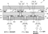
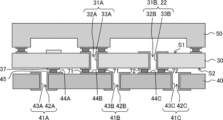
- FIG. 5 is a schematic cross-sectional view showing an example of the configuration of the quantum arithmetic device 10.
- FIG. 5 illustration of the resonator 21 (see FIG. 1) is omitted.
- FIG. 4 extracts and shows only the peripheral configuration of one quantum bit element 20 .
- the quantum arithmetic device 10 has a configuration in which a first substrate 30, a second substrate 40 and a cover 50 are laminated.
- a qubit element 20 is mounted on the first surface S1 of the first substrate 30 .
- the surface of the quantum bit element 20 is not provided with an insulating film that causes dielectric loss.
- the resonator 21, not shown in FIG. 5, can be mounted on the first surface S1 of the first substrate 30.
- the first substrate 30 is provided with through vias 31A and 31B.
- the through vias 31A and 31B include through holes 32A and 32B penetrating the first substrate 30 and conductive films 33A and 33B covering the inner walls of the through holes 32A and 32B, respectively.
- the conductive films 33A and 33B have portions extending to a second surface S2 of the first substrate 30 opposite to the first surface S1 and the first surface S2.
- the through via 31A is used to supply ground potential to the first substrate 30 and the cover 50 .
- the through via 31B functions as the readout electrode 22 .
- a control electrode 37 to which a qubit control signal for controlling the qubit element 20 is supplied is provided on the second surface S2 of the first substrate 30 .
- the control electrode 37 is arranged directly below the qubit element 20 mounted on the first surface S1, and the qubit control signal supplied to the control electrode 37 is transmitted through the base material of the first substrate 30. It is transmitted to the qubit element 20 .
- An insulator or a semiconductor can be used as the base material of the first substrate 30, and silicon, for example, can be preferably used.
- the conductive films 33A and 33B and the control electrode 37 that constitute the through vias 31A and 31B are preferably made of a metal that exhibits superconductivity at a temperature below a predetermined temperature. Nb (niobium), for example, can be suitably used as such a metal.
- the cover 50 covers the first surface S1 side of the first substrate 30 .
- the cover 50 forms an enclosed space 51 around the qubit element 20 and the readout electrode 22 .
- a concave portion for forming a closed space 51 may be formed in a portion of the cover 50 facing the qubit element 20 and the readout electrode 22 .
- the closed space 51 communicates with the through holes 32A and 32B.
- the enclosed space 51 is preferably a vacuum. By evacuating the sealed space 51, it is possible to suppress adsorption of substances to the qubit element 20 without forming a protective film that causes dielectric loss on the surface of the qubit element 20. surface can be kept clean at all times.
- the vacuum is not limited to a perfect vacuum, and includes a low-pressure state at which the effect of substantially suppressing adsorption of substances to the qubit element 20 is exhibited.
- FIG. 6 is a plan view showing an example of the form of the sealing member 60 that forms the joint between the cover 50 and the first substrate 30.
- the cover 50 is joined to the first substrate 30 via a ring-shaped sealing member 60 that surrounds the qubit element 20 and the readout electrode 22 .
- the sealed space 51 is sealed by joining the cover 50 to the first substrate 30 via the ring-shaped seal member 60 .
- the cover 50 is preferably made of a conductor, and preferably made of a metal that exhibits superconductivity at a temperature below a predetermined temperature.
- Al aluminum
- the cover 50 is joined via a bump 52 to the through via 31A to which the ground potential is supplied.
- the sealing member 60 and the bumps 52 preferably contain a metal that exhibits superconductivity at a temperature below a predetermined temperature.
- In indium
- the sealing member 60 and the bumps 52 are joined to the cover 50 via a conductive film 53 containing a metal such as Nb (niobium) that exhibits superconductivity at a temperature below a predetermined temperature.
- a metal such as Nb (niobium) that exhibits superconductivity at a temperature below a predetermined temperature.
- Nb niobium
- the second substrate 40 is provided on the second surface S2 side of the first substrate 30 .
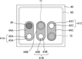
- the second substrate 40 has through vias 41A, 41B, 41C and conductive pads 44A, 44B, 44C connected to these through vias.
- the through vias 41A, 41B, 41C respectively include through holes 42A, 42B, 42C penetrating the second substrate 40 and conductive films 43A, 43B, 43C covering the inner walls of these through holes. .
- the conductive pad 44A is connected to the control electrode 37 via the bump 45.
- a qubit control signal is input from the back surface of the second substrate 40 (the surface opposite to the bonding surface with the first substrate 30), and the control electrode 37 via the through via 41A, the conductive pad 44A and the bump 45. supplied to
- the conductive pad 44B is connected to the through via 31A of the first substrate 30 via the sealing member 71.
- a ground potential is input from the back surface of the second substrate 40 and supplied to various elements formed on the first substrate 30 and the cover 50 through the through vias 41B, the conductive pads 44B, the sealing member 71 and the through vias 31A. be.
- the conductive pad 44C is connected to the through via 31B (readout electrode 22) of the first substrate 30 through the sealing member 72.
- a read control signal for reading a bit signal indicating the state of the quantum bit element 20 is input from the back surface of the second substrate 40, and passes through the through via 41C, the conductive pad 44C, and the sealing member 72 to the through via 31B (readout electrode 31B). 22).
- a bit signal read from the quantum bit element 20 is taken out to the outside following a path opposite to the path of the read control signal.
- the second substrate 40 is bonded to the first substrate 30 via bumps 45 and seal members 71 and 72 .
- FIG. 7 is a plan view showing an example of the form of the sealing members 71, 72 and the conductive pads 44B, 44C.
- the sealing members 71 and 72 have a ring shape surrounding the outer peripheries of the open ends on the second surface S2 side of the through holes 32A and 32B forming the through vias 31A and 31B of the first substrate 30, respectively.
- the through electrodes 31A and 31B are joined to the conductive pads 44B and 44C via the seal members 71 and 72, respectively, so that the open ends of the through holes 32A and 32B on the second surface S2 are closed.
- the sealed space 51 communicating with the through holes 32A and 32B is completely sealed. That is, a vacuum state is maintained in the closed space 51 .
- An insulator or a semiconductor can be used as the base material of the second substrate 40, and silicon, for example, can be preferably used.
- the sealing members 71, 72, the bumps 45, the conductive films 43A, 43B, 43C and the conductive pads 44A, 44B, 44C are each composed of a metal that exhibits superconductivity at a temperature below a predetermined temperature. is preferred.
- In (indium) can be preferably used as the metal forming the sealing members 71 and 72 and the bumps 45 .
- Nb (niobium) can be preferably used as the metal forming the conductive films 43A, 43B, 43C and the conductive pads 44A, 44B, 44C.
- the material of the second substrate 40 may be an insulator or a semiconductor. Silicon, for example, can be suitably used as the material of the second substrate 40 .
- the sealing members 71 and 72 and the bumps 45 are preferably made of metal that exhibits superconductivity at a temperature below a predetermined temperature.
- In indium
- the conductive films 43A, 43B, 43C and the conductive pads 44A, 44B, 44C forming the through vias 41A, 41B, 41C are preferably made of a metal that exhibits superconductivity at a temperature below a predetermined temperature.
- Nb (niobium) for example, can be suitably used as such a metal.
- FIG. 8 is a plan view showing an example of arrangement of the sealing member 60, the through vias 31A and 31B and the sealing members 71 and 72 associated therewith, the control electrode 37 and the bumps 45 associated therewith on the first substrate 30.
- FIG. 9 is a plan view showing an example of arrangement of through vias 41A, 41B, 41C, conductive pads 44A, 44B, 44C, and bumps 45 on the second substrate 40.
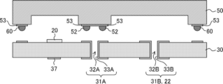
- a first substrate 30 is prepared.
- a silicon substrate can be used as the first substrate 30 .
- a resist (not shown) is formed on the surface of the first substrate 30 and patterned. Using the patterned resist as a mask, through holes 32A and 32B are formed in the first substrate 30 by deep RIE (Reactive Ion Etching), for example (FIG. 10).
- a conductive film made of a metal such as Nb (niobium) that exhibits superconductivity at a temperature equal to or lower than a predetermined critical temperature is formed on the first surface S and the second surface S2 of the first substrate 30 by a sputtering method. 33 is formed. The inner walls of the through holes 32A and 32B are also covered with the conductive film 33 (FIG. 11).
- the conductive film 33 is patterned by photolithography and dry etching. Through vias 31A and 31B and a control electrode 37 are thus formed.
- the through via 31B functions as the readout electrode 22 .
- a quantum bit element 20 including a superconducting Josephson element is formed on the first surface S1 of the first substrate 30 using Al or the like (FIG. 12).
- the cover 50 is prepared.
- the cover 50 is preferably made of a metal such as Al (aluminum) that exhibits superconductivity at a temperature equal to or lower than a predetermined critical temperature.
- a concave portion may be formed in a portion of the cover 50 that faces the qubit element 20 and the readout electrode 22 .
- a ring-shaped sealing member 60 is formed on a portion of the cover 50 surrounding the outer periphery of the quantum bit element 20 and the readout electrode 22 with a conductive film 53 interposed therebetween.
- a bump 52 is formed on the portion of the cover 50 corresponding to the through via 31A with a conductive film 53 interposed therebetween.
- the seal member 60 and the bumps 52 are preferably made of a metal such as In (indium) that exhibits superconductivity at a temperature below a predetermined critical temperature.
- the conductive film 53 is preferably made of a metal such as Nb (niobium) that exhibits superconductivity at a temperature below a predetermined critical temperature (FIG. 13).
- the cover 50 and the first substrate 30 are housed in a vacuum chamber (not shown). After that, oxides on the surface of the sealing member 60 and the bumps 52 are removed by surface treatment such as Ar ion milling in a vacuum chamber.
- the first substrate 30 and the cover 50 are heated in a vacuum chamber while being in close contact with each other.
- the heating temperature is determined according to the melting points of the sealing member 60 and the bumps 52 .
- the seal member 60 and the bumps 52 are made of, for example, In (indium), the heating temperature is preferably 100° C. or higher and 150° C. or lower.
- the sealing member 60 and the bumps 52 are melted, the first substrate 30 and the cover 50 are joined, and a sealed space 51 communicating with the through holes 32A and 32B is formed around the qubit element 20 and the readout electrode 22. be.
- the cover 50 is joined to the first substrate 30 via the ring-shaped sealing member 60 to achieve a sealed state in the sealed space 51 (FIG. 14).
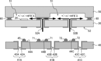
- a second substrate 40 is prepared.
- a silicon substrate for example, can be used as the second substrate 40 .
- through vias 41A, 41B, 41C and conductive pads 44A, 44B, 44C are formed in the second substrate 40 .
- These formation procedures are the same as the formation procedures of the through vias 31A and 31B in the first substrate 30 .
- bumps 45 are formed on the surfaces of the conductive pads 44A.
- seal members 71 and 72 are formed on the surfaces of the conductive pads 44B and 44C.
- the seal members 71 and 72 each have a ring-like shape surrounding the outer periphery of the opening ends of the through holes 32A and 32B on the second surface S2 side.
- the sealing members 71 and 72 and the bumps 45 are preferably made of a metal such as In (indium) that exhibits superconductivity at a temperature below a predetermined critical temperature. (Fig. 15).
- the laminate of the cover 50 and the first substrate 30 and the second substrate 40 are housed in a vacuum chamber. Thereafter, oxides on the surfaces of the seal members 71 and 72 and the bumps 45 are removed by surface treatment such as Ar ion milling. Next, a surface treatment gas such as vapor HF gas is introduced into the sealed space 51 through the through holes 32A and 32B in the vacuum chamber to remove oxides and the like from the surface of the quantum bit element 20 . As a result, the surface of the qubit element 20 is cleaned without damaging the qubit element 20 .
- a surface treatment gas such as vapor HF gas
- the first substrate 30 and the second substrate 40 are heated in a vacuum chamber while being in close contact with each other.
- the heating temperature is determined according to the melting points of the seal members 71 and 72 and the bumps 45 .
- the heating temperature is preferably 100° C. or higher and 150° C. or lower.
- the sealing members 71 and 72 and the bumps 45 are melted, and the first substrate 30 and the second substrate 40 are joined together.
- the through electrodes 31A and 31B are joined to the conductive pads 44B and 44C via the sealing members 71 and 72, respectively, so that the opening ends of the through holes 32A and 32B on the second surface S2 are closed.
- the sealed space 51 communicating with the through holes 32A and 32B is completely sealed. That is, a vacuum state is maintained in the closed space 51 (FIG. 16).
- the quantum arithmetic device 10 includes the first substrate 30 on which the quantum bit element 20 is mounted on the first surface S1, and the cover 50 covering the first surface S1 side of the first substrate 30. , and a second substrate 40 provided on the side of the second surface S2 of the first substrate 30 .
- the first substrate 30 has through holes 32A, 32B and through vias 31A, 32B including conductive films 33A, 33B.
- the cover 50 forms a closed space 51 around the qubit element 20 communicating with the through holes 32A and 32B.
- the opening ends of the through holes 32A and 32B on the second surface S2 are closed by the second substrate 40. As shown in FIG.
- the sealed space 51 is kept in a sealed state, so the surfaces of the quantum bit elements 20 can be kept clean. That is, it is possible to suppress the adsorption of substances to the surface of the qubit element 20 and avoid shortening of the coherence time due to the adsorbed substances.
- the second substrate 40 is joined to the first substrate 30 via ring-shaped seal members 71, 72 surrounding the peripheries of the open ends of the through holes 32A, 32B. is joined to the first substrate 30 via a ring-shaped sealing member 60 surrounding the .
- the sealed space 51 can be completely sealed and maintained in a vacuum state.
- adsorption of substances to the surface of the qubit element 20 can be almost completely prevented.
- the second substrate 40 includes conductive pads 44A, 44B, 44C electrically connected to the through vias 31A, 31B provided on the first substrate 30, and through vias electrically connected to these conductive pads. 41A, 41B, 41C.
- Al (aluminum), Nb (niobium) and In (indium) were exemplified as metals that exhibit superconductivity at a temperature below a predetermined critical temperature, but NbN (niobium nitride) and Ta (tantalum), TaN (tantalum nitride), and TiN (titanium nitride) can also be used.
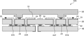
- FIG. 17 is a schematic cross-sectional view showing an example of the configuration of a quantum arithmetic device 10A according to the second embodiment of technology disclosed herein. Note that the illustration of the resonator 21 and the readout electrode 22 is omitted in FIG. Moreover, FIG. 17 extracts and shows only the configuration around one quantum bit element 20 .
- the quantum arithmetic device 10A has a configuration in which a first substrate 30, a second substrate 40 and a cover 50 are laminated, like the quantum arithmetic device 10 according to the first embodiment.
- the cover 50 forms a sealed space 51 around the qubit element 20 and covers the first surface S1 side of the first substrate 30 .
- the second substrate 40 is provided on the second surface S2 side of the first substrate 30, and each of the through holes constituting the through vias 31P, 31Q, 31R, and 31S provided in the first substrate 30. closes the open end on the side of the second surface S2.
- a plurality of quantum bit elements 20 are mounted on the first surface S ⁇ b>1 of the first substrate 30 .
- the closed spaces 51 are formed so as to be separated from each other for each quantum bit element 20 .
- FIG. 18 is a plan view showing an example of the form of the sealing member 60 that forms the joint between the cover 50 and the first substrate 30.
- the cover 50 is joined to the first substrate 30 via a ring-shaped sealing member 60 surrounding the outer periphery of each qubit element 20 .
- the sealed space 51 is sealed by joining the cover 50 to the first substrate 30 via the ring-shaped seal member 60 .
- the sealed spaces 51 provided for each quantum bit element 20 are separated from each other by a sealing member 60 .
- Each of the plurality of qubit elements 20 mounted on the first surface S1 of the first substrate 30 is connected to other adjacent qubit elements 20 via inter-bit wirings 24 .
- part of the inter-bit wiring 24 is provided on the first substrate 30, and another part of the inter-bit wiring 24 is provided on the second substrate 40.
- FIG. FIG. 18 shows a portion of the inter-bit wiring 24 provided on the first substrate 30 . As shown in FIGS. 17 and 18 , the portion of the inter-bit wiring 24 crossing the sealing member 60 is provided on the second substrate 40 , and the other portion of the inter-bit wiring 24 is provided on the first substrate 30 .
- the bit-to-bit wiring 24 detours to the second substrate 40 at the portion where it intersects the sealing member 60 .
- the portion of the inter-bit wiring 24 provided on the first substrate 30 (hereinafter referred to as the first portion) and the portion provided on the second substrate 40 (second portion) are formed by through vias 31P, 31Q and 31R. , 31S.
- the dashed arrows shown in FIG. 17 indicate paths of bit signals from the qubit element 20 to other adjacent qubit elements (not shown).
- the bit signal output from the quantum bit element 20 includes the first part of the inter-bit wiring 24, the through via 31P, the second part of the inter-bit wiring 24, the through via 31Q and the first part of the inter-bit wiring 24. portion to other adjacent qubit elements (not shown).
- the closed spaces 51 are formed so as to be separated from each other for each qubit element 20 .
- the other sealed spaces 51 can be maintained in the vacuum state. That is, compared to the case where the plurality of quantum bit elements 20 are integrally vacuum-sealed, the effect of vacuum breakage can be reduced.
- the sealing member 60 surrounding the outer periphery of each of the plurality of qubit elements 20 it is necessary to arrange the inter-bit wiring 24 so as not to contact the sealing member 60 .
- the quantum processing device 10A according to the present embodiment since the portion of the inter-bit wiring 24 intersecting the sealing member 60 bypasses the second substrate 40, contact between the inter-bit wiring 24 and the sealing member 60 is prevented. is avoided.
- FIG. 19 is a schematic cross-sectional view showing an example of the configuration of a quantum arithmetic device 10B according to the third embodiment of technology disclosed. 19, illustration of the resonator 21 and the readout electrode 22 is omitted. Moreover, FIG. 19 extracts and shows only the peripheral configuration of one quantum bit element 20 .
- FIG. 20 is a plan view showing an example of the form of the sealing member 60 that forms the joint between the cover 50 and the first substrate 30.
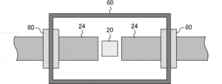
- FIG. A quantum arithmetic device 10B according to the present embodiment differs from the quantum arithmetic device 10A according to the second embodiment described above in that the entire portion of the inter-bit wiring 24 is provided on the first substrate 30 .
- an insulator 80 is provided at the intersection of the sealing member 60 and the inter-bit wiring 24 to separate the sealing member 60 and the inter-bit wiring 24 . That is, contact between the seal member 60 and the inter-bit wiring 24 is avoided by sandwiching the insulator 80 between the sealing member 60 and the inter-bit wiring 24 . According to the quantum arithmetic device 10B according to the present embodiment, through vias for detouring the inter-bit wiring 24 to the second substrate 40 are not required.
- FIG. 21 is a plan view showing an example of the pattern of the capacitors 23 provided on the path of the inter-bit wiring 24.
- the capacitor 23 may have a comb-tooth pattern as illustrated in FIG.
- the insulator 80 provided at the intersection between the sealing member 60 and the inter-bit wiring 24 may be provided at a position overlapping the capacitor 23 . Thereby, the parasitic capacitance due to the insulator 80 can be taken into the capacitor 23, and the design can be facilitated.
- the capacitors 23 may be arranged outside the area surrounded by the sealing member 60, and one capacitor 23 may be provided for two qubit elements 20 adjacent to each other.
- FIG. 22 is a schematic cross-sectional view showing an example of the configuration of a quantum arithmetic device 10C according to the fourth embodiment of technology disclosed herein.
- a quantum processing device 10C according to the fourth embodiment has a structure in which structural bodies 90A and 90B each including a cover 50, a first substrate 30 and a second substrate 40 are stacked.
- the structures 90A and 90B each have the same configuration as the quantum arithmetic device 10 according to the first embodiment described above.
- the structures 90A and 90B are laminated by joining the respective covers 50 together.
- a second substrate 40 is arranged on each of the uppermost layer and the lowermost layer of the quantum arithmetic device 10C.
- the quantum arithmetic device 10C it is possible to integrate the quantum bit elements 20 with high density.
- the second substrate 40 is arranged in the uppermost layer and the lowermost layer, wiring for accessing the quantum bit element 20 can be pulled out in two directions, and access to the quantum bit element 20 from two directions is possible. It becomes possible.
Landscapes
- Engineering & Computer Science (AREA)
- Manufacturing & Machinery (AREA)
- General Physics & Mathematics (AREA)
- Microelectronics & Electronic Packaging (AREA)
- Physics & Mathematics (AREA)
- Theoretical Computer Science (AREA)
- Mathematical Analysis (AREA)
- Computing Systems (AREA)
- Evolutionary Computation (AREA)
- Condensed Matter Physics & Semiconductors (AREA)
- Computational Mathematics (AREA)
- Mathematical Optimization (AREA)
- Pure & Applied Mathematics (AREA)
- Data Mining & Analysis (AREA)
- General Engineering & Computer Science (AREA)
- Mathematical Physics (AREA)
- Software Systems (AREA)
- Artificial Intelligence (AREA)
- Internal Circuitry In Semiconductor Integrated Circuit Devices (AREA)
- Superconductor Devices And Manufacturing Methods Thereof (AREA)
- Semiconductor Memories (AREA)
Priority Applications (4)
| Application Number | Priority Date | Filing Date | Title |
|---|---|---|---|
| JP2023572319A JP7666652B2 (ja) | 2022-01-07 | 2022-01-07 | 量子演算装置及び量子演算装置の製造方法 |
| PCT/JP2022/000384 WO2023132063A1 (ja) | 2022-01-07 | 2022-01-07 | 量子演算装置及び量子演算装置の製造方法 |
| EP22918652.3A EP4475176B1 (en) | 2022-01-07 | 2022-01-07 | Quantum computing device and method for manufacturing quantum computing device |
| US18/734,686 US20260082822A1 (en) | 2022-01-07 | 2024-06-05 | Quantum operation device and method of manufacturing quantum operation device |
Applications Claiming Priority (1)
| Application Number | Priority Date | Filing Date | Title |
|---|---|---|---|
| PCT/JP2022/000384 WO2023132063A1 (ja) | 2022-01-07 | 2022-01-07 | 量子演算装置及び量子演算装置の製造方法 |
Related Child Applications (1)
| Application Number | Title | Priority Date | Filing Date |
|---|---|---|---|
| US18/734,686 Continuation US20260082822A1 (en) | 2022-01-07 | 2024-06-05 | Quantum operation device and method of manufacturing quantum operation device |
Publications (1)
| Publication Number | Publication Date |
|---|---|
| WO2023132063A1 true WO2023132063A1 (ja) | 2023-07-13 |
Family
ID=87073584
Family Applications (1)
| Application Number | Title | Priority Date | Filing Date |
|---|---|---|---|
| PCT/JP2022/000384 Ceased WO2023132063A1 (ja) | 2022-01-07 | 2022-01-07 | 量子演算装置及び量子演算装置の製造方法 |
Country Status (4)
| Country | Link |
|---|---|
| US (1) | US20260082822A1 (https=) |
| EP (1) | EP4475176B1 (https=) |
| JP (1) | JP7666652B2 (https=) |
| WO (1) | WO2023132063A1 (https=) |
Cited By (2)
| Publication number | Priority date | Publication date | Assignee | Title |
|---|---|---|---|---|
| WO2025046715A1 (ja) * | 2023-08-28 | 2025-03-06 | 富士通株式会社 | 量子ビットデバイス及び量子ビットデバイスの製造方法 |
| EP4590108A1 (en) * | 2024-01-18 | 2025-07-23 | Fujitsu Limited | Method for manufacturing qubit device |
Citations (7)
| Publication number | Priority date | Publication date | Assignee | Title |
|---|---|---|---|---|
| JPH04338683A (ja) * | 1991-05-16 | 1992-11-25 | Fujitsu Ltd | 超伝導集積回路素子とその実装方法 |
| JPH11177157A (ja) * | 1997-12-08 | 1999-07-02 | Agency Of Ind Science & Technol | 超電導集積回路構造及びその製造方法 |
| US20180013052A1 (en) * | 2015-07-23 | 2018-01-11 | Massachusetts Institute Of Technology | Qubit and Coupler Circuit Structures and Coupling Techniques |
| JP2019532520A (ja) | 2016-09-14 | 2019-11-07 | グーグル エルエルシー | ローカル真空キャビティーを使用して量子デバイスの中の散逸および周波数ノイズを低減させること |
| JP2019532505A (ja) * | 2016-09-13 | 2019-11-07 | グーグル エルエルシー | 積層量子デバイス内の損失の低減 |
| JP2020511794A (ja) | 2017-03-13 | 2020-04-16 | グーグル エルエルシー | 積層型量子コンピューティングデバイスにおける回路要素の集積 |
| JP2021072351A (ja) * | 2019-10-30 | 2021-05-06 | 日本電気株式会社 | 超伝導回路装置、スペーサ、及び超伝導回路装置の製造方法 |
Family Cites Families (2)
| Publication number | Priority date | Publication date | Assignee | Title |
|---|---|---|---|---|
| US6528875B1 (en) * | 2001-04-20 | 2003-03-04 | Amkor Technology, Inc. | Vacuum sealed package for semiconductor chip |
| US9836699B1 (en) * | 2015-04-27 | 2017-12-05 | Rigetti & Co. | Microwave integrated quantum circuits with interposer |
-
2022
- 2022-01-07 JP JP2023572319A patent/JP7666652B2/ja active Active
- 2022-01-07 WO PCT/JP2022/000384 patent/WO2023132063A1/ja not_active Ceased
- 2022-01-07 EP EP22918652.3A patent/EP4475176B1/en active Active
-
2024
- 2024-06-05 US US18/734,686 patent/US20260082822A1/en active Pending
Patent Citations (7)
| Publication number | Priority date | Publication date | Assignee | Title |
|---|---|---|---|---|
| JPH04338683A (ja) * | 1991-05-16 | 1992-11-25 | Fujitsu Ltd | 超伝導集積回路素子とその実装方法 |
| JPH11177157A (ja) * | 1997-12-08 | 1999-07-02 | Agency Of Ind Science & Technol | 超電導集積回路構造及びその製造方法 |
| US20180013052A1 (en) * | 2015-07-23 | 2018-01-11 | Massachusetts Institute Of Technology | Qubit and Coupler Circuit Structures and Coupling Techniques |
| JP2019532505A (ja) * | 2016-09-13 | 2019-11-07 | グーグル エルエルシー | 積層量子デバイス内の損失の低減 |
| JP2019532520A (ja) | 2016-09-14 | 2019-11-07 | グーグル エルエルシー | ローカル真空キャビティーを使用して量子デバイスの中の散逸および周波数ノイズを低減させること |
| JP2020511794A (ja) | 2017-03-13 | 2020-04-16 | グーグル エルエルシー | 積層型量子コンピューティングデバイスにおける回路要素の集積 |
| JP2021072351A (ja) * | 2019-10-30 | 2021-05-06 | 日本電気株式会社 | 超伝導回路装置、スペーサ、及び超伝導回路装置の製造方法 |
Non-Patent Citations (1)
| Title |
|---|
| See also references of EP4475176A4 |
Cited By (2)
| Publication number | Priority date | Publication date | Assignee | Title |
|---|---|---|---|---|
| WO2025046715A1 (ja) * | 2023-08-28 | 2025-03-06 | 富士通株式会社 | 量子ビットデバイス及び量子ビットデバイスの製造方法 |
| EP4590108A1 (en) * | 2024-01-18 | 2025-07-23 | Fujitsu Limited | Method for manufacturing qubit device |
Also Published As
| Publication number | Publication date |
|---|---|
| EP4475176A1 (en) | 2024-12-11 |
| JP7666652B2 (ja) | 2025-04-22 |
| US20260082822A1 (en) | 2026-03-19 |
| EP4475176B1 (en) | 2026-04-29 |
| EP4475176A4 (en) | 2025-10-29 |
| JPWO2023132063A1 (https=) | 2023-07-13 |
Similar Documents
| Publication | Publication Date | Title |
|---|---|---|
| US12217129B2 (en) | Integrating circuit elements in a stacked quantum computing device | |
| US20260082822A1 (en) | Quantum operation device and method of manufacturing quantum operation device | |
| US12518977B2 (en) | Signal distribution for a quantum computing system | |
| EP3937093B1 (en) | Quantum computing circuit comprising a plurality of chips and method for manufacturing the same | |
| JP7819759B2 (ja) | 量子デバイス及び量子デバイスの製造方法 | |
| JP7666653B2 (ja) | 量子演算装置及び量子演算装置の製造方法 | |
| EP4703979A1 (en) | Quantum computing device and method for manufacturing quantum computing device | |
| JP2024106984A (ja) | キュービットチップ素子及びその製造方法 | |
| US20260068537A1 (en) | Quantum bit device and method for manufacturing quantum bit device | |
| US20250169380A1 (en) | Qubit chip device and method of manufacturing the same | |
| US20250275488A1 (en) | Device and manufacturing method for device | |
| US20250200415A1 (en) | Qubit device and qubit device fabrication method | |
| US20250309092A1 (en) | Device and method of manufacturing device | |
| JP2026044162A (ja) | 量子ビットデバイス及び量子ビットデバイスの製造方法 | |
| KR20240117866A (ko) | 조셉슨 접합 소자, 조셉슨 접합 소자를 포함하는 초전도 큐비트, 및 조셉슨 접합 소자의 제조 방법 | |
| JP2026044161A (ja) | 量子ビットデバイス及び量子ビットデバイスの製造方法 | |
| JPS58125880A (ja) | ジヨセフソン接合素子 | |
| JPS5889877A (ja) | 超伝導回路装置 |
Legal Events
| Date | Code | Title | Description |
|---|---|---|---|
| ENP | Entry into the national phase |
Ref document number: 2023572319 Country of ref document: JP Kind code of ref document: A |
|
| WWE | Wipo information: entry into national phase |
Ref document number: 2022918652 Country of ref document: EP |
|
| NENP | Non-entry into the national phase |
Ref country code: DE |
|
| ENP | Entry into the national phase |
Ref document number: 2022918652 Country of ref document: EP Effective date: 20240807 |
|
| 121 | Ep: the epo has been informed by wipo that ep was designated in this application |
Ref document number: 22918652 Country of ref document: EP Kind code of ref document: A1 |
|
| 121 | Ep: the epo has been informed by wipo that ep was designated in this application |
Ref document number: 22918652 Country of ref document: EP Kind code of ref document: A1 |