WO2023132001A1 - 光電変換装置、光電変換システム、および移動体 - Google Patents
光電変換装置、光電変換システム、および移動体 Download PDFInfo
- Publication number
- WO2023132001A1 WO2023132001A1 PCT/JP2022/000069 JP2022000069W WO2023132001A1 WO 2023132001 A1 WO2023132001 A1 WO 2023132001A1 JP 2022000069 W JP2022000069 W JP 2022000069W WO 2023132001 A1 WO2023132001 A1 WO 2023132001A1
- Authority
- WO
- WIPO (PCT)
- Prior art keywords
- photoelectric conversion
- region
- conversion device
- semiconductor element
- substrate
- Prior art date
- Legal status (The legal status is an assumption and is not a legal conclusion. Google has not performed a legal analysis and makes no representation as to the accuracy of the status listed.)
- Ceased
Links
Images


Classifications
-
- H—ELECTRICITY
- H10—SEMICONDUCTOR DEVICES; ELECTRIC SOLID-STATE DEVICES NOT OTHERWISE PROVIDED FOR
- H10F—INORGANIC SEMICONDUCTOR DEVICES SENSITIVE TO INFRARED RADIATION, LIGHT, ELECTROMAGNETIC RADIATION OF SHORTER WAVELENGTH OR CORPUSCULAR RADIATION
- H10F39/00—Integrated devices, or assemblies of multiple devices, comprising at least one element covered by group H10F30/00, e.g. radiation detectors comprising photodiode arrays
- H10F39/10—Integrated devices
- H10F39/12—Image sensors
- H10F39/18—Complementary metal-oxide-semiconductor [CMOS] image sensors; Photodiode array image sensors
- H10F39/182—Colour image sensors
-
- H—ELECTRICITY
- H10—SEMICONDUCTOR DEVICES; ELECTRIC SOLID-STATE DEVICES NOT OTHERWISE PROVIDED FOR
- H10F—INORGANIC SEMICONDUCTOR DEVICES SENSITIVE TO INFRARED RADIATION, LIGHT, ELECTROMAGNETIC RADIATION OF SHORTER WAVELENGTH OR CORPUSCULAR RADIATION
- H10F39/00—Integrated devices, or assemblies of multiple devices, comprising at least one element covered by group H10F30/00, e.g. radiation detectors comprising photodiode arrays
- H10F39/10—Integrated devices
- H10F39/12—Image sensors
- H10F39/199—Back-illuminated image sensors
-
- H—ELECTRICITY
- H10—SEMICONDUCTOR DEVICES; ELECTRIC SOLID-STATE DEVICES NOT OTHERWISE PROVIDED FOR
- H10F—INORGANIC SEMICONDUCTOR DEVICES SENSITIVE TO INFRARED RADIATION, LIGHT, ELECTROMAGNETIC RADIATION OF SHORTER WAVELENGTH OR CORPUSCULAR RADIATION
- H10F39/00—Integrated devices, or assemblies of multiple devices, comprising at least one element covered by group H10F30/00, e.g. radiation detectors comprising photodiode arrays
- H10F39/80—Constructional details of image sensors
- H10F39/803—Pixels having integrated switching, control, storage or amplification elements
- H10F39/8033—Photosensitive area
-
- H—ELECTRICITY
- H10—SEMICONDUCTOR DEVICES; ELECTRIC SOLID-STATE DEVICES NOT OTHERWISE PROVIDED FOR
- H10F—INORGANIC SEMICONDUCTOR DEVICES SENSITIVE TO INFRARED RADIATION, LIGHT, ELECTROMAGNETIC RADIATION OF SHORTER WAVELENGTH OR CORPUSCULAR RADIATION
- H10F39/00—Integrated devices, or assemblies of multiple devices, comprising at least one element covered by group H10F30/00, e.g. radiation detectors comprising photodiode arrays
- H10F39/80—Constructional details of image sensors
- H10F39/805—Coatings
- H10F39/8057—Optical shielding
-
- H—ELECTRICITY
- H10—SEMICONDUCTOR DEVICES; ELECTRIC SOLID-STATE DEVICES NOT OTHERWISE PROVIDED FOR
- H10F—INORGANIC SEMICONDUCTOR DEVICES SENSITIVE TO INFRARED RADIATION, LIGHT, ELECTROMAGNETIC RADIATION OF SHORTER WAVELENGTH OR CORPUSCULAR RADIATION
- H10F39/00—Integrated devices, or assemblies of multiple devices, comprising at least one element covered by group H10F30/00, e.g. radiation detectors comprising photodiode arrays
- H10F39/80—Constructional details of image sensors
- H10F39/809—Constructional details of image sensors of hybrid image sensors
-
- H—ELECTRICITY
- H10—SEMICONDUCTOR DEVICES; ELECTRIC SOLID-STATE DEVICES NOT OTHERWISE PROVIDED FOR
- H10F—INORGANIC SEMICONDUCTOR DEVICES SENSITIVE TO INFRARED RADIATION, LIGHT, ELECTROMAGNETIC RADIATION OF SHORTER WAVELENGTH OR CORPUSCULAR RADIATION
- H10F39/00—Integrated devices, or assemblies of multiple devices, comprising at least one element covered by group H10F30/00, e.g. radiation detectors comprising photodiode arrays
- H10F39/80—Constructional details of image sensors
- H10F39/811—Interconnections
-
- H—ELECTRICITY
- H04—ELECTRIC COMMUNICATION TECHNIQUE
- H04N—PICTORIAL COMMUNICATION, e.g. TELEVISION
- H04N25/00—Circuitry of solid-state image sensors [SSIS]; Control thereof
- H04N25/70—SSIS architectures; Circuits associated therewith
- H04N25/703—SSIS architectures incorporating pixels for producing signals other than image signals
- H04N25/705—Pixels for depth measurement, e.g. RGBZ
Definitions
- the present invention relates to a photoelectric conversion device, a photoelectric conversion system, and a moving body.
- Patent Literature 1 discloses a back-illuminated photoelectric conversion device.
- a back-illuminated photoelectric conversion device is disclosed in which light is irradiated from a surface of a semiconductor substrate opposite to a surface on which a wiring layer is arranged.
- charge discharging pixels for discharging signal charges leaking from the effective pixel region are arranged between the effective pixel region and the OB region, or in the OB region. It is Then, signal charges leaking from the effective pixel area are forcibly discharged.
- Patent Document 1 considers the surplus charge that enters the OB region from the effective pixel region, it does not consider the surplus charge that enters the OB region from the periphery of the OB region. That is, when OB pixels are arranged at the edge of the substrate as in Patent Document 1, when signal charges generated around the OB region are mixed into the OB region, the reference signal of the black level fluctuates. It is also necessary to suppress mixing of surplus charges into the OB region. In particular, in the case of a stacked photoelectric conversion device, there is no need to dispose a signal processing circuit for processing signals output from pixels around the OB region, so the effect of the present invention becomes more pronounced.
- Patent Document 1 does not discuss the case where, among the plurality of photoelectric conversion units arranged in the passing pixel area, a photoelectric conversion unit having a larger shielded area than other photoelectric conversion units is included.
- a first substrate having a first semiconductor element layer including a plurality of photoelectric conversion units and a well in which the plurality of photoelectric conversion units are arranged; a second substrate having a second semiconductor element layer including a circuit for processing the received signal, wherein the first substrate and the second substrate are laminated, and the first semiconductor element layer includes the plurality of an effective pixel region having a photoelectric conversion portion of; an optical black pixel region provided between the effective pixel region and an end of the first semiconductor element and having the plurality of photoelectric conversion portions; and the optical black pixel and a peripheral region arranged between the region and an edge of the first semiconductor element layer, wherein the effective pixel region is shielded from light more than the other photoelectric conversion units among the plurality of photoelectric conversion units.
- the optical black pixel region overlaps with a light shielding region constituted by a light shielding layer, and the outer peripheral region does not overlap with the light shielding region. and a charge discharge region including a semiconductor region of the same conductivity type as that of signal charges is provided in the peripheral region, and a fixed potential is supplied to the charge discharge region.
- the present invention it is possible to provide a stacked photoelectric conversion device capable of suppressing the mixture of surplus electric charges in the OB region and more accurately detecting the reference signal of the black level.
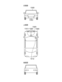
- FIG. 4A and 4B are schematic diagrams of semiconductor substrates of the photoelectric conversion device according to Embodiment 1.
- FIG. FIG. 2 is a schematic top view of a semiconductor substrate according to Embodiment 1;
- FIG. 3 is a schematic cross-sectional view taken along line XX′ of FIG. 2;
- FIG. 2 is a schematic top view of a semiconductor substrate according to Embodiment 2;
- 5 is a schematic cross-sectional view taken along line XX' of FIG. 4;
- FIG. 10 is a schematic top view of a semiconductor substrate according to Embodiment 3;
- 7 is a schematic cross-sectional view taken along line XX' of FIG. 6;
- FIG. 4 is a schematic cross-sectional view of a photoelectric conversion device according to Embodiment 4.
- FIG. 6 is a schematic cross-sectional view of a photoelectric conversion device according to Embodiment 5.
- FIG. FIG. 11 is a schematic cross-sectional view of a photoelectric conversion device according to Embodiment 6;
- FIG. 11 is a schematic plan view of a light shielding layer of a photoelectric conversion device according to Embodiment 6;
- FIG. 12 is a schematic plan view of another example of the light shielding layer of the photoelectric conversion device according to Embodiment 6;
- FIG. 11 is an equivalent circuit diagram of a pixel in Embodiment 7;
- FIG. 12 is a diagram showing the configuration of a pixel according to Embodiment 7;
- FIG. 12 is a diagram showing the configuration of a pixel according to Embodiment 7;
- FIG. 12 is a diagram showing the configuration of a pixel according to Embodiment 7;
- FIG. 11 is an equivalent circuit diagram of a pixel in Embodiment 7;
- FIG. 12 is a diagram showing the
- FIG. 12 is a diagram showing the configuration of a pixel according to Embodiment 7;
- FIG. 11 is a schematic cross-sectional view of a photoelectric conversion device according to Embodiment 7;
- FIG. 11 is a schematic plan view of a light shielding layer of a photoelectric conversion device according to Embodiment 7;
- FIG. 11 is a block diagram of a photoelectric conversion system according to Embodiment 8;
- FIG. 11 is a block diagram of a photoelectric conversion system according to an embodiment related to Embodiment 9;
- FIG. 11 is a block diagram of a photoelectric conversion system according to an embodiment related to Embodiment 9;
- 10 is a flowchart of a photoelectric conversion system according to an embodiment related to Embodiment 9;
- the semiconductor region of the first conductivity type having majority carriers of the same conductivity type as the signal charges is the N-type semiconductor region, and the semiconductor region of the second conductivity type is the P-type semiconductor region. Note that the present invention is established even when the signal charges are holes.
- the semiconductor region of the first conductivity type having majority carriers of the same conductivity type as the signal charges is a P-type semiconductor region, and the semiconductor region of the second conductivity type is an N-type semiconductor region.
- impurity concentration when the term "impurity concentration” is simply used, it means the net impurity concentration compensated for by impurities of the opposite conductivity type. In other words, “impurity concentration” refers to NET doping concentration.
- a region in which the P-type impurity concentration is higher than the N-type impurity concentration is a P-type semiconductor region.
- a region where the N-type impurity concentration is higher than the P-type impurity concentration is an N-type semiconductor region.
- planar view refers to viewing from a direction perpendicular to a light incident surface of a semiconductor substrate, which will be described later.
- cross section refers to a plane in a direction perpendicular to the light incident surface of the semiconductor substrate.
- the depth direction is the direction from the light incident surface (first surface) of the semiconductor substrate toward the surface (second surface) on which the transistors are arranged.
- FIG. 1 shows a photoelectric conversion device 500 according to the first embodiment.
- a photoelectric conversion device is a semiconductor device IC.
- the photoelectric conversion device 500 according to this embodiment can be used as, for example, an image sensor, a photometry sensor, or a distance measurement sensor.
- the photoelectric conversion device 500 is a laminated photoelectric conversion device in which all or part of the substrate 1 and the substrate 2 are laminated and joined.
- the substrates 1 and 2 may be in the state of chips obtained by dicing the wafer after lamination, or may be in the state of wafers.
- the photoelectric conversion device 500 is a stacked back-illuminated photoelectric conversion device.
- the substrate 1 has a semiconductor element layer 11 (first semiconductor element layer) including pixel circuits included in the pixels 10, and a wiring structure 12 (first wiring structure).
- semiconductor element layer includes not only a semiconductor layer but also a semiconductor layer and a gate of a transistor formed in the semiconductor layer.
- the wiring layer of the wiring structure is not included in the "semiconductor element layer”.
- the substrate 2 has a wiring structure 24 (second wiring structure) and a semiconductor element layer 23 (second semiconductor element layer) including an electric circuit.
- the wiring structure 12 of the substrate 1 and the wiring structure 24 of the substrate 2 are joined by a metal joint formed by joining the wiring layers included in each wiring structure.
- a metal joint portion is a structure in which a metal forming a wiring layer and a metal forming a wiring layer are directly joined.
- the elements forming the pixels 10 are arranged in the semiconductor element layer 11 .
- a part of the structure of the pixel 10 may be arranged in the semiconductor element layer 11 and the other part of the structure may be arranged in the semiconductor element layer.
- the configuration of the pixel circuit arranged in the semiconductor element layer 11 of the pixel 10 includes a photoelectric conversion element such as a photodiode.
- Pixel circuits including photoelectric conversion elements are arranged in a two-dimensional array on the semiconductor element layer 11 in plan view.
- the semiconductor element layer 11 has a pixel region in which a plurality of pixel circuits are arranged in a two-dimensional array. In FIG. 1, the semiconductor element layer 11 has a plurality of photoelectric conversion elements forming a plurality of pixel circuits arranged in a two-dimensional array in row and column directions.
- the wiring structure 12 includes M (M is an integer equal to or greater than 1) wiring layers and an interlayer insulating material.
- the wiring structure 24 includes N (N is an integer equal to or greater than 1) wiring layers and an interlayer insulating material.
- the semiconductor element layer 23 includes an electric circuit that processes signals obtained by the photoelectric conversion units arranged in the semiconductor element layer 11 .
- the electric circuit is, for example, any one of the transistors constituting the row scanning circuit 20, the column scanning circuit 21, the signal processing circuit 22, etc. shown in FIG.
- the signal processing circuit 22 includes, for example, a part of the configuration of the pixel 10 such as an amplification transistor, a selection transistor, and a reset transistor, an amplification circuit, a selection circuit, a logical operation circuit, an AD conversion circuit, a memory, compression processing, synthesis processing, and the like. at least one of the circuits that
- a pixel 10 can refer to the smallest circuit unit that is repeatedly arranged to form an image.
- a pixel circuit included in the pixel 10 and arranged on the semiconductor element layer 11 may include at least a photoelectric conversion element.
- the pixel circuit may include components other than the photoelectric conversion element.
- the pixel circuit may further include at least one of a transfer transistor, FD, reset transistor, amplification transistor, capacitance addition transistor, and selection transistor.
- a pixel 10 is composed of a selection transistor and a group of elements connected to a signal line via the selection transistor. That is, the selection transistor can be the outer edge of the pixel circuit.
- the pixel 10 may be composed of a set of a photoelectric conversion element and a transfer transistor.
- the pixel 10 may be composed of a set of one or more photoelectric conversion elements and one amplifier circuit or one AD conversion circuit.
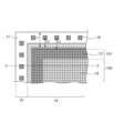
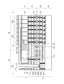
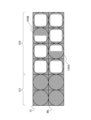
- FIG. 2 shows a schematic top view of the end portion of the semiconductor element layer 11 in Embodiment 1.
- the pixel area of the semiconductor element layer 11 includes an effective pixel area 100 in which effective pixels using incident signal charges as signals are arranged, and an optical black pixel (OB pixel) in which an optical black pixel (OB pixel) for detecting a black level reference value is arranged.
- OB pixel optical black pixel
- a black pixel region 101 is provided.
- the OB pixel region 101 is arranged around the effective pixel region 100 in a plan view, and is provided with a light blocking layer 13 that blocks light incident on the photoelectric conversion units in the OB pixel region 101 . In other words, in plan view, the OB pixel region overlaps with the light shielding region configured by the light shielding layer.
- the periphery does not have to be the entire periphery, and may be at least one of the top, bottom, left, and right of the effective pixel area 100 .
- the term “periphery” also includes what is not the entire circumference, unless otherwise specified.
- “light shielding” is not limited to blocking 100% of light. For example, it refers to something that blocks 50% or more of light.
- a well region 14 and a peripheral region 15 located around the well region 14 are arranged inside the semiconductor element layer 11 .
- the light-shielding region formed by the light-shielding layer 13 does not overlap the outer peripheral region 15 .
- the outer peripheral area 15 and the light shielding area do not completely overlap in plan view, but they may partially overlap as in an embodiment described later.
- At least a portion of pixel 10 is formed in well region 14 .
- a pad portion 16 is provided in the outer peripheral region 15 .
- the pad portion 16 is arranged between the edge of the semiconductor element layer 11 and the well region 14 .
- the shortest distance L1 between the semiconductor element layer 11 and the light shielding layer 13 is, for example, 100 ⁇ m or more and 250 ⁇ m or less, preferably 100 ⁇ m or more and 150 ⁇ m or less.
- the shortest distance L2 between the center of the pad portion 16 and the light shielding layer 13 in plan view is, for example, 30 ⁇ m or more and 200 ⁇ m or less, and preferably 50 ⁇ m or more and 100 ⁇ m or less. In order to avoid formation defects due to manufacturing errors when forming the pads, it is necessary to separate them by a predetermined distance or more.
- the center of the pad portion 16 refers to the center of the pad trench. Further, although the details will be described later, the closer the distance between the center of the pad portion 16 and the OB pixel region 101 is, the more remarkable the effect of the present embodiment is.
- the shortest distance L3 between the center of the pad portion 16 and the pixel 10 in the OB pixel region 101 is, for example, 100 ⁇ m or more and 500 ⁇ m or less, preferably 250 ⁇ m or more and 350 ⁇ m or less.
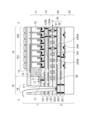
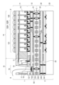
- FIG. 3 shows a schematic cross-sectional view of the X-X' cross section in FIG.
- the substrate 1 and the substrate 2 are bonded together at the bonding surface 3 and laminated.
- the wiring structure 12 of the substrate 1 and the wiring structure 24 of the substrate 2 are located.
- the wiring structure 12 has three wiring layers 121 , 122 and 123
- the wiring structure 24 has three wiring layers 241 , 242 and 243 .
- the wiring structure 12 has three wiring layers of wiring layers 121 , 122 and 123 .
- the wiring layers 121, 122, 123 can be Cu wiring layers, for example.
- the wiring layer 123 constitutes the metal portion 31 of the metal joint portion 30 .
- the metal junction 30 is embedded in a recess formed in the interlayer insulating film and has a damascene structure.
- the wiring structure 24 has three wiring layers of wiring layers 241, 242, and 243.
- the wiring layers 241, 242 and 243 may be Cu wiring layers.
- the wiring layer 243 constitutes the metal portion 32 of the metal junction portion 30 .
- the metal part 32 is embedded in a recess formed in the interlayer insulating film and has a damascene structure.
- the inter-layer insulating film having the concave portion in which the metal portion 31 is embedded, the inter-layer insulating film having the concave portion in which the metal portion 32 is embedded, and the metal portion 31 and the metal portion 32 are joined (contacted).
- the metal joint portion 30 is formed by joining the metal portion 31 and the metal portion 32 .
- the via plug 124 formed in the interlayer insulating film of the wiring layer 123 makes the metal portion 31 and the wiring layer 122 conductive.
- a via plug 244 formed in the interlayer insulating film of the wiring layer 243 electrically connects the metal portion 32 and the wiring layer 242 . Electrical connection between the semiconductor element layer 11 and the semiconductor element layer 23 is established at the metal junction 30 to which the via plugs 124 and 244 are connected.
- the wiring layer 123 includes a wiring pattern 123a connected to the wiring pattern of the upper wiring layer, and a wiring pattern 123b not connected to the wiring pattern of the upper layer.
- the wiring layer 243 includes a wiring pattern 243a connected to the underlying wiring pattern and a wiring pattern 243b not connected to the underlying wiring pattern.
- the wiring pattern 123a is connected through the via plug 124 to the upper wiring pattern.
- the wiring pattern 243a is connected to the underlying wiring pattern through the via plug 244 .
- the via plug is not essential, and the wiring pattern and the upper or lower wiring pattern may be connected by being in direct contact with each other.
- the wiring patterns 123a and 243a electrically connect the semiconductor element layer 11 and the semiconductor element layer 23 .
- the wiring patterns 123a and 243a need to connect the semiconductor element layer 11 and the semiconductor element layer 23, and some wiring patterns 123a and 243a are connected to the semiconductor element layer 11 or the semiconductor element layer 23. good too.
- some of the wiring patterns 123a and 243a may be connected to any wiring layer and may not be connected to either the semiconductor element layer 11 or the semiconductor element layer 23.
- the semiconductor element layer 11 has a well region 14 in which a well 19 is arranged, and an outer peripheral region 15 located between the edge of the semiconductor element layer 11 and the well region 14 .
- the well 19 is, for example, a region implanted with P-type impurity ions
- the peripheral region 15 is a region where the well 19 is not arranged.
- the peripheral region 15 is an N-type semiconductor region or a region having a lower P-type impurity concentration than the well 19 .
- a plurality of photoelectric conversion units in the effective pixel area 100 and a plurality of photoelectric conversion units in the OB pixel area 101 are arranged in the well 19 .
- An effective pixel region 100 and an OB pixel region 101 are arranged in the well region 14 .
- the light shielding layer 13 is arranged on the side of the light incident surface of the semiconductor element layer 11 .
- the light shielding layer is arranged on the light incident surface of the semiconductor element layer 11 via an insulating material, for example.
- a microlens is arranged on the side of the light incident surface of the semiconductor element layer 11 via an insulating material. Also, in FIG. 5, a color filter is arranged between the microlens and the insulating material.
- the arrangement of the color filters can be selected as appropriate. For example, it may be a Bayer array. Also, a plurality of photoelectric conversion units may be arranged for one microlens.
- the OB pixel area 101 is also provided with microlenses, but the microlenses are not essential. A configuration in which no microlens is arranged at a position overlapping the light shielding layer 13 in a plan view may be adopted. As shown in FIG. 3, the light shielding layer 13 may be arranged between a certain pixel 10 and an adjacent pixel 10 in a plan view in the effective pixel region 100 . Thereby, crosstalk between pixels in the effective pixel area 100 can be reduced.
- a pad portion 16 is arranged in the outer peripheral region 15 . As shown in FIG. 2 , a plurality of pad portions 16 are arranged in the outer peripheral region 15 .
- the plurality of pad portions 16 conduct electricity between the photoelectric conversion device 500 and a signal processing device or the like arranged outside the photoelectric conversion device.
- the plurality of pad sections 16 include a pad section for outputting a signal from the photoelectric conversion device 500 to the outside and a pad section for inputting a power supply voltage or the like to the photoelectric conversion device 500 .
- a trench that will become the pad section 16 is formed at the end of the semiconductor element layer 11 .
- the trench is formed in the depth direction from the light incident surface of the semiconductor element layer 11 to a depth reaching the wiring pattern of the wiring layer 242 of the substrate 2 .
- the pad portion 16 is electrically connected to the wiring layer 242 formed on the substrate 2 by wire bonding.
- the wiring layer 242 can be an Al wiring layer.
- the entire wiring layer 242 need not be made of Al, and only the wiring to which the pad section 16 is connected may be made of Al wiring, and the other wiring may be made of Cu wiring.
- a through via (TSV) in which a trench is filled with a metal may be used.
- the trench of the pad section 16 may be formed with a depth reaching the wiring layer of the substrate 1 .
- the thickness (length in the depth direction) of the semiconductor element layer 11 tends to be smaller than that of a front-illuminated photoelectric conversion device.
- the thickness of the semiconductor element layer 11 is 11 ⁇ m or less. Therefore, long-wavelength light such as infrared light incident from the light incident surface of the semiconductor element layer 11 is more likely to be reflected by the surface on which the transistor is formed and generate surplus electric charges. In particular, as shown in FIG.
- a drain portion 17 is provided for discharging surplus electric charges in the outer peripheral region 15 .
- the drain portion 17 functions as a charge discharge region for discharging surplus charges.
- a semiconductor region 171 of the same conductivity type as that of the peripheral region 15 is arranged in the drain portion 17 .
- the semiconductor region 171 can be formed by ion-implanting impurities of the same conductivity type as the peripheral region 15 .
- the semiconductor region 171 is a region with a higher impurity concentration than the peripheral region 15 .
- a contact plug 172 is formed in the semiconductor region 171 .
- a fixed potential is applied to the drain portion 17 through the wiring layer 121 and the contact plug 172 .
- the peripheral region 15 when the peripheral region 15 is N-type and the well region 14 is P-type, a positive power supply voltage is applied.
- a negative power supply voltage is applied.
- the peripheral region 15 is P-type
- ground potential is applied. Therefore, surplus electric charges can be discharged from the drain portion 17, and by creating a potential difference with the well region 14, electric charges can be prevented from being mixed into the OB pixel region 101.
- FIG. Similarly, charges generated as dark current at the edge of the substrate can also be prevented from entering the OB pixel region 101 . Therefore, it is possible to accurately detect the reference value of the black level.
- the semiconductor region 171 and the well 19 are arranged as close as possible.
- the distance between the semiconductor region 171 and the well 19 is preferably 0 ⁇ m or more and 100 ⁇ m or less. This makes it easier to suppress surplus charges such as charges photoelectrically converted near the well 19 in the peripheral region 15 and noise charges (dark current) from entering the OB pixel region 101 through the well 19 . .
- a wiring pattern common to the wiring pattern supplied to the drain of the transistor of the pixel may be used.
- the wiring pattern supplied with the VDD power of the reset transistor and the wiring pattern supplied with the VDD power supplied to the drain section 17 may be shared.
- pad portions 16 are arranged between the upper end of the semiconductor element layer 11 and the well region 14 and between the left end of the semiconductor element layer 11 and the well region 14 in plan view.
- the pad portion 16 may be arranged between the lower end of the semiconductor element layer 11 and the well region 14 and between the right end of the semiconductor element layer 11 and the well region 14 in plan view. That is, the outer peripheral region 15 in which the pad portions 16 are arranged may be arranged so as to surround the entire circumference of the well region 14 of the semiconductor element layer 11 in plan view. In such a case, the area where the light shielding layer 13 is not provided between the OB pixel region 101 and the peripheral region 15 tends to increase, so that the reference value of the black level can be detected more accurately.
- the pad portion 16 is arranged so as to surround the entire circumference of the well region 14 of the semiconductor element layer 11 in plan view. Even if the pad portion 16 is not arranged in this manner, the effects of the present invention can be obtained as long as the pad portion 16 is arranged at least partly between the end of the semiconductor element layer 11 and the well region 14 in plan view. can be obtained.
- the pad portion 16 is arranged between the upper end of the semiconductor element layer 11 and the well region 14, and the pad portion 16 is not arranged between the left end of the semiconductor element layer 11 and the well region 14. It's okay. Even in this case, it is possible to obtain the effect that the reference value of the black level can be detected more accurately.
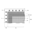
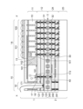
- FIG. 4 shows a schematic top view of the edge of the semiconductor element layer 11 in the second embodiment.
- 5 shows a schematic cross-sectional view of the XX' cross section in FIG.
- the present embodiment differs from the first embodiment in that the light shielding layer 13 is arranged so as to cover the well region 14 . Since this point and points other than those described below are substantially the same as those of the first embodiment, the description thereof is omitted.
- the light shielding layer 13 is arranged so as to partially overlap the outer peripheral region 15 in plan view. That is, in a cross-sectional view, the light shielding layer 13 protrudes from the end of the well region 14 toward the pad section 16 side.
- Embodiment 1 since part of the well region 14 is not shielded from light, surplus charges photoelectrically converted in the well region 14 may enter the adjacent OB pixel region 101 .
- the well region 14 since the well region 14 is shielded from light, photoelectric conversion does not occur in the well region 14 .
- the well 19 is not exposed from the light shielding region in plan view. In other words, in plan view, the edge of the well 19 and the edge of the light shielding layer 13 are at the same position, or the edge of the light shielding layer 13 protrudes from the edge of the well 19 to the semiconductor element layer 11 side.
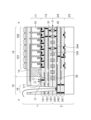
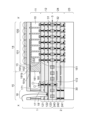
- FIG. 6 shows a schematic top view of the edge of the semiconductor element layer 11 in the third embodiment.
- 7 shows a schematic cross-sectional view of the XX' cross section in FIG.
- This embodiment differs from the second embodiment in that an isolation region 18 is arranged around the pad portion 16 of the semiconductor element layer 11 . Except for this point and the matters described below, since it is substantially the same as the second embodiment, the description is omitted.
- the separation region 18 is arranged so as to surround the entire circumference of the pad portion 16 in plan view.
- the isolation region 18 is an isolation region in which trenches formed in the semiconductor element layer 11 are filled with an insulating film such as a silicon oxide film or a silicon nitride film.
- the separation region 18 separates the peripheral region 15 between the vicinity of the trench of the pad portion 16 and the vicinity of the well 19 . That is, the side surface of the trench of the semiconductor element layer 11 in which the pad portion 16 is formed is insulated by the isolation region 18 from the peripheral region 15 where the drain portion 17 is arranged and the voltage is applied. Therefore, as in the second embodiment, it is possible to avoid short-circuiting between the wire bonding and the peripheral region 15 while detecting the black level reference value more accurately.
- FIG. 8 shows a schematic cross-sectional view of a stacked back-illuminated photoelectric conversion device according to the fourth embodiment.
- the semiconductor element layer 11 includes an avalanche photodiode (hereinafter referred to as APD).
- APD avalanche photodiode
- the distance L4 between the semiconductor region 161 of the second conductivity type to which the APD drive voltage is applied and the semiconductor region 171 discharging surplus charges is the distance between the well 19 and the semiconductor region 171 in the third embodiment. It differs from the third embodiment in that it is larger than . Except for these points and the points to be described below, it is substantially the same as the third embodiment, so the description is omitted.
- the APD arranged on the substrate 1 is composed of a semiconductor region 151 of a first conductivity type and a semiconductor region 152 of a second conductivity type.
- the avalanche-multiplied charge is transferred to the substrate 2 via the metal junction 30 .
- a quench circuit, a counter circuit, and the like are arranged on the substrate 2 , and a signal is sent to the counter circuit and the like of the substrate 2 through the metal joint 30 . Therefore, a metal junction 30 connecting the semiconductor element layer 11 and the semiconductor element layer 23 is arranged for each APD.
- the semiconductor region 152 of the second conductivity type In order to drive the APD, it is necessary to apply a high voltage to the semiconductor region 152 of the second conductivity type.
- the difference between the voltage applied to the semiconductor region 151 and the voltage applied to the semiconductor region 152 is, for example, 20 V or more.
- An example of the voltage applied to the semiconductor region 152 is a negative voltage with an absolute value greater than -20V.
- the voltage applied to the semiconductor region 152 is supplied from the semiconductor region 161 of the second conductivity type through the semiconductor region 153 of the second conductivity type. Therefore, the above-described high voltage is applied to the semiconductor region 161 of the second conductivity type.
- the semiconductor region 171 for discharging surplus electric charges is formed of the first conductivity type, if the semiconductor region 161 of the second conductivity type is close to the semiconductor region 161, the semiconductor region 171 and the semiconductor region 171 are separated from each other. An avalanche multiplication region is formed between. That is, there is a possibility that an avalanche multiplication region is formed in a region other than the pixel region, and surplus charges are avalanche multiplied and enter the OB pixel region 101 .
- the distance L4 between the second-conductivity-type semiconductor region 161 surrounding the pixel region and the first-conductivity-type semiconductor region 171 is set to a value such that avalanche multiplication does not occur. It should be set to distance.
- the black level reference value can be accurately detected while suppressing the formation of the avalanche multiplication region between the semiconductor regions 161 and 171. can be done.
- the distance L4 can be, for example, 1 ⁇ m or more and 10 ⁇ m or less, preferably 3 ⁇ m or more and 6 ⁇ m or less.
- the semiconductor region 171 and the light shielding layer 13 may overlap in plan view.
- FIG. 9 shows a schematic cross-sectional view of a stacked back-illuminated photoelectric conversion device according to the fifth embodiment.
- This embodiment differs from the fourth embodiment in that the drain portion 17 and the pad portion 16 are connected within the same substrate. Since this point and points other than those described below are substantially the same as those of the fourth embodiment, the description thereof is omitted.
- the trenches of the pad section 16 are formed with a depth reaching the wiring pattern of the wiring layer 122 of the substrate 1, and the wiring pattern of the wiring layer 122 is connected to the bonding wire. Then, the wiring pattern to which the bonding wire is connected and the drain portion 17 are connected via the contact plug 172 and the wiring pattern of the wiring layer 121 .
- the photoelectric conversion unit arranged on the substrate 1 is an APD
- a high voltage is required to drive the APD.
- the substrate 2 is generally formed by a fine process, it is not preferable from the standpoint of withstand voltage to apply the high voltage for driving the APD to the semiconductor element layer 23 of the substrate 2 . Therefore, it is preferable that the high voltage for driving the APD is supplied from the pads arranged on the substrate 1 . In this case, the surplus charges discharged from the drain portion 17 of the substrate 1 are discharged to the outside of the photoelectric conversion device through the pad portion 16 arranged on the substrate 1 .
- the depth of the trench of the pad portion 16 for supplying the drive voltage of the element arranged on the substrate 2 and the depth of the trench of the pad portion 16 for supplying the drive voltage of the APD arranged on the substrate 1 are different. may complicate the process and increase the difficulty of the process.
- voltages for driving the elements arranged on the substrate 2 are also applied to the pads formed on the substrate 1 and then applied to the semiconductor element layer 23 of the substrate 2 via the metal joints 40 . preferably supplied.
- the black level reference value is accurately detected while suppressing the formation of the avalanche multiplication region between the semiconductor regions 161 and 171. be able to. Moreover, since a high voltage is not applied to the semiconductor element layer 23 of the substrate 2, it becomes easier to ensure the reliability of the photoelectric conversion device when using the APD.
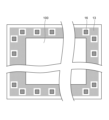
- FIG. 10 shows a schematic cross-sectional view of a stacked back-illuminated photoelectric conversion device according to Embodiment 6, and FIG. 1 shows a plan view.
- FIG. 11 the positions of the via plugs are also illustrated in order to make it easier to understand the positions of the via plugs in plan view.
- This embodiment is different in that the semiconductor region 161 of the second conductivity type and the light shielding layer 13 are connected via via plugs 191a, 191b, and 191c. Another difference is that color filters of different colors are arranged. Other than these points, it is substantially the same as the fifth embodiment, so the description is omitted.
- the light shielding layer 13 and the second conductivity type semiconductor region 161 are electrically connected to the via plugs 191a, 191b and 191c.
- a high voltage which is a negative voltage whose absolute value is greater than -20 V, is applied to the second conductivity type semiconductor region 161 .
- This voltage is also applied to the light shielding layer 13 through via plugs 191a, 191b, and 191c. That is, the light shielding layer 13 and the semiconductor region 161 are at the same potential. If there is a large potential difference between the semiconductor region 161 and the light shielding layer 13, there is a possibility that dielectric breakdown will occur in the insulating film interposed between the light shielding layer 13 and the semiconductor region 161. Dielectric breakdown in the film can be suppressed.
- the light shielding layer 13 and the semiconductor region 161 are connected by three via plugs in FIG. 10, they may be connected by one or two via plugs, or may be connected by four or more via plugs.
- the semiconductor region 161 is preferably arranged so as to be wider than the pixel region including the OB pixel region 101 .
- the width of the semiconductor region 161 is wider than the width of the pixel region in a cross-sectional view. This makes it easier to connect the light shielding layer 13 and the semiconductor region 161 through the via plug.
- FIG. 10 shows only one cross section, it is preferable that the width of the semiconductor region 161 is wider than the width of the pixel region 100 also in the cross section in the direction intersecting the cross section of FIG.
- the second conductivity type semiconductor region 152 forming the avalanche multiplication region of the APD may be arranged over the entire pixel region in plan view. In that case, the end portion of the second conductivity type semiconductor region 152 may be included in the second conductivity type semiconductor region 161 or may be in contact with the outer peripheral portion of the second conductivity type semiconductor region 161 . .
- the light shielding layer 13 is arranged so as to partially surround the opening of the pad section 16 in plan view.
- the light shielding layer 13 is arranged so as to surround three of the four sides forming the square in plan view.
- the light shielding layer 13 is arranged as far as the edge of the semiconductor element layer 11 as much as possible.
- via plugs 191a, 191b, and 191c are arranged so as to surround the effective pixel area 100 and the OB pixel area 101 in plan view.
- the via plugs 191a and 191b and the semiconductor region 161 are also connected in the cross section in the direction intersecting the cross section of FIG.
- the light shielding layer 13 may be arranged so as to surround the entire circumference of the pad portion 16 in plan view. As a result, the amount of light entering the semiconductor element layer 11 can be reduced more than the example shown in FIG.
- FIG. 12 does not show the via plugs 191a, 191b, and 191c shown in FIG. 11, the via plugs 191a, 191b, and 191c may be arranged. Also, an OB pixel region 101 shown in FIG. 11 may be arranged.
- the black level reference value is accurately detected while suppressing the formation of the avalanche multiplication region between the semiconductor regions 161 and 171. be able to. Moreover, since a high voltage is not applied to the semiconductor element layer 23 of the substrate 2, it becomes easier to ensure the reliability of the photoelectric conversion device when using the APD. Furthermore, dielectric breakdown of the insulating film arranged between the light shielding layer 13 and the semiconductor region 161 can be suppressed.
- FIG. 7 is an equivalent circuit diagram of a pixel in Embodiment 7
- FIGS. 14A to 14C are diagrams showing the configuration of a pixel in Embodiment 7
- FIG. 15 is a schematic top view of well region 14 in Embodiment 8.
- there is 16 shows a schematic cross-sectional view of a cross section corresponding to the XX' cross section of FIG.
- This embodiment differs from Embodiments 1 to 3 in that each pixel 10 has a plurality of photoelectric conversion units and is configured to be able to perform phase difference detection type focus detection. . Except for this point and the matters described below, the description is substantially the same as that of the other embodiments, so the description is omitted.
- FIG. 13 is a circuit diagram showing an example of a circuit of the pixels 10 arranged in two rows and one column among the pixels 10 arranged in the effective pixel area 100.
- FIG. 13 is a circuit diagram showing an example of a circuit of the pixels 10 arranged in two rows and one column among the pixels 10 arranged in the effective pixel area 100.
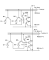
- the pixel 10 has photodiodes D1 and D2, which are photoelectric conversion units, transfer transistors M1 and M2, a charge conversion unit C1, a reset transistor M3, an amplification transistor M4, and a selection transistor M5.
- the transfer transistor M1 is provided in an electrical path between the photodiode D1 and a node to which the charge converter C1, the reset transistor M3, and the amplification transistor M4 are connected.
- the transfer transistor M2 is provided in an electrical path between the node to which the charge converter C1, the reset transistor M3, and the amplification transistor M4 are connected, and the photodiode D2.
- the charge conversion section C1 is also called a floating diffusion section (FD section).
- a power supply voltage VDD is applied to the reset transistor M3 and the amplification transistor M4.
- the selection transistor M5 is provided in an electrical path between the amplification transistor M4 and the vertical output line 50.
- FIG. It can be said that the amplification transistor M4 is electrically connected to the vertical output line 50 via the selection transistor M5.
- the charge conversion unit C1 includes a floating diffusion capacitance provided in the semiconductor substrate and a parasitic capacitance of an electrical path from the transfer transistor M1 to the amplification transistor M5 via the floating diffusion capacitance.
- Each of the signal RES, the signal Tx_A, and the signal SEL is a signal supplied from a vertical scanning circuit (not shown).
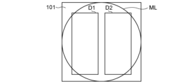
- the photodiodes D1 and D2 are arranged corresponding to one microlens ML, as shown in FIG. 14A. That is, the photodiodes D1 and D2 are arranged to receive the light transmitted through one microlens ML. Accordingly, phase difference detection type focus detection can be performed.
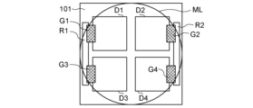
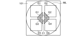
- FIGS. 14B and 14C show a configuration in which four photodiodes D1 to D4 are provided as four photoelectric conversion units for one microlens ML.
- a transfer transistor is provided corresponding to each of the photodiodes D1 to D4, and the gates G1 to G4 are gate electrodes of the corresponding transfer transistors.
- FIG. 14B gates G1, G3 transfer charge to pixel readout circuit R1.
- Gates G2 and G4 transfer charge to pixel readout circuit R2.
- Each of the pixel readout circuits R1 and R2 is provided with the capacitive element C1 shown in FIG.
- FIG. 14C shows a form in which gates G1 to G4 are provided to transfer charges to one capacitive element C1. Even in such a form, the present embodiment can be suitably implemented.
- FIG. 15 shows a schematic top view of the well region 14 in the eighth embodiment.
- the light shielding layer 13 provided on the well region 14 shields the OB pixel region 101 from light.
- the portion of the light shielding layer 13 that overlaps the effective pixel region 100 in plan view is provided with an aperture corresponding to the pixel, and light enters the corresponding pixel.
- one of the photodiodes D1 and D2 is shielded from light, and light is allowed to enter the other.
- the light-shielding layer 13 shown in FIG. 15 includes apertures corresponding to the pixels 100A having the photodiodes D2 in FIG. 14A and pixels 100B corresponding to the pixels 100B having the photodiodes D1 in FIG. 14A.
- light enters one of the photodiodes D1 and D2 for some of the pixels 10, and enters the other of the photodiodes D1 and D2 for some other pixels 10.
- phase difference detection type focus detection can be performed by reading the signals of some of the pixels 10 and some of the other pixels 10 .
- the read signal is used for focus detection by a detector provided on the second substrate, for example. Only by changing the pattern of the light shielding layer 13, pixels for phase difference detection can be formed without increasing the number of steps.
- the pixel 100A may include only one photodiode. In this case, for some of the pixels 10, part of the photodiode is shielded from light and light is allowed to enter the other part. Then, for another part of the pixels 10, a part of the photodiode at another position is shielded from light, and light is allowed to enter the other part.
- the light-shielded area is larger than that of the photodiode used for imaging.
- Focus detection can be performed by the output signal of the pixel 10 having the light-shielded photodiode.
- FIG. 16 shows a schematic cross-sectional view of a cross section corresponding to the X-X' cross section in FIG.
- the effective pixels provided in the effective pixel area 100 have pixels 100A and pixels 100B.
- the structure of the pad portion 16 is changed with respect to the cross-sectional view shown in FIG.
- the wiring structure 12 includes a first wiring layer 121 , a second wiring layer 122 and a connecting portion 31 .
- the wiring structure 24 includes a first wiring layer 242 , a second wiring layer 241 and a connecting portion 32 .
- Each wiring layer is a so-called copper wiring.
- the first wiring layer includes a conductor pattern whose main component is copper.
- the conductor pattern of the wiring layer 1 has a single damascene structure.
- a contact is provided for electrical connection between the first wiring layer and the semiconductor layer 11 .
- a contact is a conductor pattern whose main component is tungsten.
- the second wiring layer includes a conductor pattern containing copper as a main component.
- the conductor pattern of the second wiring layer has a dual damascene structure and includes portions functioning as wiring and portions functioning as vias.
- the pad electrode 60 included in the pad portion 16 is a conductor pattern whose main component is aluminum.
- the pad electrode 60 is provided in the second wiring layer of the wiring structure 12 and positioned between the first surface and the second surface of the first substrate, but the position of the pad electrode 60 is not limited to this. .
- the pad electrode 60 has a first surface and a second surface opposite to the first surface.
- the first surface is partially exposed through an opening in the semiconductor layer.
- the exposed portion of the pad electrode 60 can function as a connection portion with an external terminal, a so-called pad portion.
- the pad electrode 60 is connected on its second surface to a plurality of copper-based conductors.
- the pad electrode 60 may have a via made of a conductor mainly composed of aluminum, and may be electrically connected to a conductor mainly composed of copper located on the first surface side through the via. good. Also, the pad electrode 60 may be connected to the first wiring layer of the wiring structure 303 on the first surface by a conductor mainly composed of tungsten.
- the pad electrode 60 is formed by forming an insulator covering the wiring layer, removing a part of the insulator, forming a film mainly composed of aluminum to be the pad electrode 60, and patterning the film. can be done.
- the pad electrode 60 After forming the copper wiring, it is possible to form the pad electrode 60 having a large film thickness while maintaining the flatness of the fine copper wiring.
- the pad electrode 60 of the present embodiment is included in the wiring structure 12, it may be included in the wiring structure 24. Also, the position where the pad electrode is provided may be either of the wiring structures 121 and 122, and is not limited. The material and structure of each wiring layer of the wiring structures 121 and 122 are not limited to those illustrated, and for example, a conductor layer may be further provided between the wiring layer 1 and the semiconductor layer. Also, the contact may have a stack contact structure in which two layers are laminated.
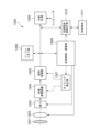
- FIG. 17 is a block diagram showing the configuration of a photoelectric conversion system 1200 according to this embodiment.
- a photoelectric conversion system 1200 of this embodiment includes a photoelectric conversion device 1204 .
- any of the photoelectric conversion devices described in the above embodiments can be applied to the photoelectric conversion device 1204 .
- the photoelectric conversion system 1200 can be used, for example, as an imaging system. Specific examples of imaging systems include digital still cameras, digital camcorders, surveillance cameras, and the like.
- FIG. 17 shows an example of a digital still camera as the photoelectric conversion system 1200 .
- a photoelectric conversion system 1200 shown in FIG. 17 includes a photoelectric conversion device 1204, a lens 1202 for forming an optical image of a subject on the photoelectric conversion device 1204, an aperture 1203 for varying the amount of light passing through the lens 1202, and protection of the lens 1202. has a barrier 1201 for A lens 1202 and a diaphragm 1203 are an optical system for condensing light onto the photoelectric conversion device 1204 .
- the photoelectric conversion system 1200 has a signal processing unit 1205 that processes the output signal output from the photoelectric conversion device 1204 .
- the signal processing unit 1205 performs a signal processing operation of performing various corrections and compressions on an input signal and outputting the signal as necessary.
- the photoelectric conversion system 1200 further includes a buffer memory section 1206 for temporarily storing image data, and an external interface section (external I/F section) 1209 for communicating with an external computer or the like.
- the photoelectric conversion system 1200 includes a recording medium 1211 such as a semiconductor memory for recording or reading image data, and a recording medium control interface section (recording medium control I/F section) for recording or reading the recording medium 1211. 1210.
- the recording medium 1211 may be built in the photoelectric conversion system 1200, or may be detachable. Communication from the recording medium control I/F unit 1210 to the recording medium 1211 and communication from the external I/F unit 1209 may be performed wirelessly.
- the photoelectric conversion system 1200 further includes an overall control/calculation unit 1208 that performs various calculations and controls the entire digital still camera, and a timing generation unit 1207 that outputs various timing signals to the photoelectric conversion device 1204 and signal processing unit 1205 .
- a timing signal or the like may be input from the outside, and the photoelectric conversion system 1200 may include at least a photoelectric conversion device 1204 and a signal processing unit 1205 that processes an output signal output from the photoelectric conversion device 1204. good.
- the timing generator 1207 may be mounted in the photoelectric conversion device as described in the fourth embodiment.
- the overall control/calculation unit 1208 and the timing generation unit 1207 may be configured to implement part or all of the control functions of the photoelectric conversion device 1204 .
- the photoelectric conversion device 1204 outputs the image signal to the signal processing unit 1205 .
- a signal processing unit 1205 performs predetermined signal processing on the image signal output from the photoelectric conversion device 1204 and outputs image data. Also, the signal processing unit 1205 generates an image using the image signal. Also, the signal processing unit 1205 may perform ranging calculation on the signal output from the photoelectric conversion device 1204 .
- the signal processing unit 1205 and the timing generation unit 1207 may be mounted on the photoelectric conversion device. That is, the signal processing unit 1205 and the timing generation unit 1207 may be provided on the substrate on which the pixels are arranged, or may be provided on another substrate.
- FIG. 18A and 18B are schematic diagrams showing configuration examples of a photoelectric conversion system and a moving object according to this embodiment.
- FIG. 19 is a flowchart showing the operation of the photoelectric conversion system according to this embodiment. In this embodiment, an example of an in-vehicle camera is shown as a photoelectric conversion system.
- FIGs. 18A and 18B show an example of a vehicle system and a photoelectric conversion system mounted therein for imaging.
- a photoelectric conversion system 1301 includes a photoelectric conversion device 1302 , an image preprocessing unit 1315 , an integrated circuit 1303 and an optical system 1314 .
- An optical system 1314 forms an optical image of a subject on the photoelectric conversion device 1302 .
- the photoelectric conversion device 1302 converts the optical image of the subject formed by the optical system 1314 into an electrical signal.
- the photoelectric conversion device 1302 is the photoelectric conversion device according to any one of the embodiments described above.
- An image preprocessing unit 1315 performs predetermined signal processing on the signal output from the photoelectric conversion device 1302 .
- the functions of the image preprocessing unit 1315 may be incorporated within the photoelectric conversion device 1302 .
- the photoelectric conversion system 1301 is provided with at least two sets of an optical system 1314, a photoelectric conversion device 1302, and an image preprocessing unit 1315, and the output from each set of image preprocessing units 1315 is input to an integrated circuit 1303. It's like
- the integrated circuit 1303 is an integrated circuit for use in imaging systems, and includes an image processing unit 1304 including a memory 1305, an optical distance measurement unit 1306, a distance calculation unit 1307, an object recognition unit 1308, and an abnormality detection unit 1309.
- An image processing unit 1304 performs image processing such as development processing and defect correction on the output signal of the image preprocessing unit 1315 .
- a memory 1305 temporarily stores captured images and stores defect positions of captured pixels.
- An optical distance measurement unit 1306 performs focusing of a subject and distance measurement.
- a ranging calculation unit 1307 calculates ranging information from a plurality of image data acquired by a plurality of photoelectric conversion devices 1302 .
- the object recognition unit 1308 recognizes subjects such as cars, roads, signs, and people.
- the abnormality detection unit 1309 detects an abnormality in the photoelectric conversion device 1302, the abnormality detection unit 1309 notifies the main control unit 1313 of the abnormality.
- the integrated circuit 1303 may be realized by specially designed hardware, software modules, or a combination thereof. Also, it may be realized by FPGA (Field Programmable Gate Array), ASIC (Application Specific Integrated Circuit), etc., or by a combination thereof.
- FPGA Field Programmable Gate Array
- ASIC Application Specific Integrated Circuit
- the main control unit 1313 integrates and controls the operations of the photoelectric conversion system 1301, the vehicle sensor 1310, the control unit 1320, and the like. There is also a method in which the photoelectric conversion system 1301, the vehicle sensor 1310, and the control unit 1320 have individual communication interfaces without having the main control unit 1313, and each of them transmits and receives control signals via a communication network (for example, CAN standard).
- a communication network for example, CAN standard
- the integrated circuit 1303 has a function of receiving a control signal from the main control unit 1313 or transmitting a control signal and setting values to the photoelectric conversion device 1302 by its own control unit.
- the photoelectric conversion system 1301 is connected to a vehicle sensor 1310, and can detect the running state of the own vehicle such as vehicle speed, yaw rate, and steering angle, the environment outside the own vehicle, and the state of other vehicles and obstacles.
- the vehicle sensor 1310 also serves as distance information acquisition means for acquiring distance information to an object.
- the photoelectric conversion system 1301 is also connected to a driving support control unit 1311 that performs various driving support functions such as automatic steering, automatic cruise, and anti-collision functions.
- the collision determination function based on the detection results of the photoelectric conversion system 1301 and the vehicle sensor 1310, it is possible to estimate a collision with another vehicle/obstacle and determine whether or not there is a collision. As a result, avoidance control when a collision is presumed and safety device activation at the time of collision are performed.
- the photoelectric conversion system 1301 is also connected to an alarm device 1312 that issues an alarm to the driver based on the judgment result of the collision judgment section. For example, if the judgment result of the collision judging section indicates that the possibility of collision is high, the main control section 1313 controls the vehicle to avoid collision and reduce damage by applying the brakes, releasing the accelerator, or suppressing the engine output. conduct.
- the alarm device 1312 warns the user by sounding an alarm such as sound, displaying alarm information on a display unit screen of a car navigation system or a meter panel, or vibrating a seat belt or steering wheel.
- the photoelectric conversion system 1301 photographs the surroundings of the vehicle, for example, the front or rear.
- FIG. 18B shows an arrangement example of the photoelectric conversion system 1301 when the photoelectric conversion system 1301 captures an image in front of the vehicle.
- the two photoelectric conversion devices 1302 are arranged in front of the vehicle 1300 . Specifically, if the center line of the vehicle 1300 with respect to the direction of movement or the outer shape (for example, the width of the vehicle) is regarded as the axis of symmetry, and the two photoelectric conversion devices 1302 are arranged line-symmetrically with respect to the axis of symmetry, the vehicle 1300 and This is preferable for obtaining information on the distance to the object to be photographed and for determining the possibility of collision. Moreover, the photoelectric conversion device 1302 is preferably arranged so as not to obstruct the driver's field of vision when the driver visually recognizes the situation outside the vehicle 1300 from the driver's seat. It is preferable that the warning device 1312 be arranged so as to be easily visible to the driver.
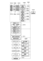
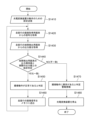
- the failure detection operation of photoelectric conversion device 1302 in the photoelectric conversion system 1301 will be described using FIG.
- the failure detection operation of photoelectric conversion device 1302 is performed according to steps S1410 to S1480 shown in FIG.
- Step S1410 is a step for performing settings at startup of the photoelectric conversion device 1302 . That is, the settings for the operation of the photoelectric conversion device 1302 are transmitted from outside the photoelectric conversion system 1301 (for example, the main control unit 1313) or inside the photoelectric conversion system 1301, and the imaging operation and failure detection operation of the photoelectric conversion device 1302 are performed. Start.
- step S1420 pixel signals are obtained from effective pixels. Also, in step S1430, an output value is obtained from a failure detection pixel provided for failure detection.
- This failure detection pixel has a photoelectric conversion section like the effective pixel. A predetermined voltage is written in the photoelectric conversion unit. The failure detection pixel outputs a signal corresponding to the voltage written to the photoelectric conversion section. Note that steps S1420 and S1430 may be reversed.
- step S1440 it is determined whether the expected output value of the failure-detected pixel and the actual output value from the failure-detected pixel match.
- step S1450 it is determined that the imaging operation is performed normally, and the processing step proceeds to step S1460. and migrate.
- step S1460 the pixel signals of the scanning line are transmitted to the memory 1305 for temporary storage. After that, the process returns to step S1420 to continue the failure detection operation.
- the process proceeds to step S1470.
- step S1470 it is determined that there is an abnormality in the imaging operation, and an alarm is issued to the main control unit 1313 or the alarm device 1312.
- FIG. The alarm device 1312 causes the display unit to display that an abnormality has been detected.
- step S1480 the photoelectric conversion device 1302 is stopped, and the operation of the photoelectric conversion system 1301 ends.
- step S1470 may be notified to the outside of the vehicle via a wireless network.
- the control that does not collide with another vehicle has been described, but it is also applicable to control that automatically drives following another vehicle, control that automatically drives so as not to stray from the lane, and the like.
- the photoelectric conversion system 1301 can be applied not only to a vehicle such as a vehicle, but also to a moving object (moving device) such as a ship, an aircraft, or an industrial robot.
- the present invention can be applied not only to mobile objects but also to devices that widely use object recognition, such as intelligent transportation systems (ITS).
- ITS intelligent transportation systems
- the photoelectric conversion device of the present invention may further have a configuration capable of acquiring various information such as distance information.
Landscapes
- Solid State Image Pick-Up Elements (AREA)
Priority Applications (3)
| Application Number | Priority Date | Filing Date | Title |
|---|---|---|---|
| PCT/JP2022/000069 WO2023132001A1 (ja) | 2022-01-05 | 2022-01-05 | 光電変換装置、光電変換システム、および移動体 |
| JP2023572271A JP7767466B2 (ja) | 2022-01-05 | 2022-01-05 | 光電変換装置、光電変換システム、および移動体 |
| US18/762,474 US20240355857A1 (en) | 2022-01-05 | 2024-07-02 | Photoelectric conversion apparatus, photoelectric conversion system, and moving object |
Applications Claiming Priority (1)
| Application Number | Priority Date | Filing Date | Title |
|---|---|---|---|
| PCT/JP2022/000069 WO2023132001A1 (ja) | 2022-01-05 | 2022-01-05 | 光電変換装置、光電変換システム、および移動体 |
Related Child Applications (1)
| Application Number | Title | Priority Date | Filing Date |
|---|---|---|---|
| US18/762,474 Continuation US20240355857A1 (en) | 2022-01-05 | 2024-07-02 | Photoelectric conversion apparatus, photoelectric conversion system, and moving object |
Publications (1)
| Publication Number | Publication Date |
|---|---|
| WO2023132001A1 true WO2023132001A1 (ja) | 2023-07-13 |
Family
ID=87073440
Family Applications (1)
| Application Number | Title | Priority Date | Filing Date |
|---|---|---|---|
| PCT/JP2022/000069 Ceased WO2023132001A1 (ja) | 2022-01-05 | 2022-01-05 | 光電変換装置、光電変換システム、および移動体 |
Country Status (3)
| Country | Link |
|---|---|
| US (1) | US20240355857A1 (enExample) |
| JP (1) | JP7767466B2 (enExample) |
| WO (1) | WO2023132001A1 (enExample) |
Citations (3)
| Publication number | Priority date | Publication date | Assignee | Title |
|---|---|---|---|---|
| JP2011151461A (ja) * | 2010-01-19 | 2011-08-04 | Hoya Corp | 固体撮像素子 |
| CN113473050A (zh) * | 2020-03-31 | 2021-10-01 | 佳能株式会社 | 光电转换装置、光电转换系统和移动物体 |
| JP2021176154A (ja) * | 2018-07-18 | 2021-11-04 | ソニーセミコンダクタソリューションズ株式会社 | 受光素子および測距モジュール |
-
2022
- 2022-01-05 WO PCT/JP2022/000069 patent/WO2023132001A1/ja not_active Ceased
- 2022-01-05 JP JP2023572271A patent/JP7767466B2/ja active Active
-
2024
- 2024-07-02 US US18/762,474 patent/US20240355857A1/en active Pending
Patent Citations (3)
| Publication number | Priority date | Publication date | Assignee | Title |
|---|---|---|---|---|
| JP2011151461A (ja) * | 2010-01-19 | 2011-08-04 | Hoya Corp | 固体撮像素子 |
| JP2021176154A (ja) * | 2018-07-18 | 2021-11-04 | ソニーセミコンダクタソリューションズ株式会社 | 受光素子および測距モジュール |
| CN113473050A (zh) * | 2020-03-31 | 2021-10-01 | 佳能株式会社 | 光电转换装置、光电转换系统和移动物体 |
Also Published As
| Publication number | Publication date |
|---|---|
| JP7767466B2 (ja) | 2025-11-11 |
| JPWO2023132001A1 (enExample) | 2023-07-13 |
| US20240355857A1 (en) | 2024-10-24 |
Similar Documents
| Publication | Publication Date | Title |
|---|---|---|
| US12396274B2 (en) | Photoelectric conversion apparatus, photoelectric conversion system, and moving object | |
| US11843014B2 (en) | Photoelectric conversion apparatus having metal portion, imaging system, movable body, and semiconductor chip for stacking | |
| US12356738B2 (en) | Semiconductor apparatus and device | |
| US20250201639A1 (en) | Semiconductor device, manufacturing method thereof, and electronic apparatus | |
| US12176340B2 (en) | Photoelectric conversion apparatus having semiconductor substrates and protection circuits | |
| US10692915B2 (en) | Imaging device and method of manufacturing imaging device | |
| JP2021125491A (ja) | 半導体装置、半導体システム、移動体 | |
| US20250072144A1 (en) | Photoelectric conversion apparatus, photoelectric conversion system, and moving body | |
| JP7558822B2 (ja) | 光電変換装置、光電変換システム、および移動体 | |
| US11095843B2 (en) | Imaging devices and imaging apparatuses, and methods for the same | |
| JP2022087547A (ja) | 光電変換装置、光電変換システム、および移動体 | |
| JP7767466B2 (ja) | 光電変換装置、光電変換システム、および移動体 | |
| US20230069364A1 (en) | Photoelectric conversion apparatus having capacitance addition transistor, photoelectric conversion system, and movable body | |
| US12137297B2 (en) | Imaging devices and imaging apparatuses, and methods for the same | |
| US20250311474A1 (en) | Semiconductor apparatus, photoelectric conversion system and moving body | |
| US20230387157A1 (en) | Photoelectric conversion device, manufacturing method of photoelectric conversion device, imaging system, moving unit, and equipment | |
| JP2021019058A (ja) | 光電変換装置および機器 | |
| JP2025155801A (ja) | 半導体装置及び光電変換システム | |
| JP2025005684A (ja) | 光電変換装置、光電変換システムおよび移動体 |
Legal Events
| Date | Code | Title | Description |
|---|---|---|---|
| WWE | Wipo information: entry into national phase |
Ref document number: 2023572271 Country of ref document: JP |
|
| NENP | Non-entry into the national phase |
Ref country code: DE |
|
| 122 | Ep: pct application non-entry in european phase |
Ref document number: 22918593 Country of ref document: EP Kind code of ref document: A1 |