WO2023132001A1 - Photoelectric conversion device, photoelectric conversion system, and mobile body - Google Patents
Photoelectric conversion device, photoelectric conversion system, and mobile body Download PDFInfo
- Publication number
- WO2023132001A1 WO2023132001A1 PCT/JP2022/000069 JP2022000069W WO2023132001A1 WO 2023132001 A1 WO2023132001 A1 WO 2023132001A1 JP 2022000069 W JP2022000069 W JP 2022000069W WO 2023132001 A1 WO2023132001 A1 WO 2023132001A1
- Authority
- WO
- WIPO (PCT)
- Prior art keywords
- photoelectric conversion
- region
- conversion device
- semiconductor element
- substrate
- Prior art date
Links
- 238000006243 chemical reaction Methods 0.000 title claims abstract description 192
- 239000004065 semiconductor Substances 0.000 claims abstract description 168
- 239000000758 substrate Substances 0.000 claims abstract description 72
- 230000002093 peripheral effect Effects 0.000 claims abstract description 42
- 238000012545 processing Methods 0.000 claims abstract description 30
- 238000001514 detection method Methods 0.000 claims description 27
- 230000003287 optical effect Effects 0.000 claims description 19
- 239000010949 copper Substances 0.000 claims description 11
- 238000000034 method Methods 0.000 claims description 11
- 230000008569 process Effects 0.000 claims description 10
- RYGMFSIKBFXOCR-UHFFFAOYSA-N Copper Chemical compound [Cu] RYGMFSIKBFXOCR-UHFFFAOYSA-N 0.000 claims description 8
- 229910052802 copper Inorganic materials 0.000 claims description 8
- 238000007599 discharging Methods 0.000 claims description 8
- 239000011810 insulating material Substances 0.000 claims description 6
- 238000002955 isolation Methods 0.000 claims description 6
- 229910052782 aluminium Inorganic materials 0.000 claims description 4
- XAGFODPZIPBFFR-UHFFFAOYSA-N aluminium Chemical compound [Al] XAGFODPZIPBFFR-UHFFFAOYSA-N 0.000 claims description 4
- 230000005611 electricity Effects 0.000 claims description 2
- 239000010410 layer Substances 0.000 description 176
- 229910052751 metal Inorganic materials 0.000 description 25
- 239000002184 metal Substances 0.000 description 25
- 238000010586 diagram Methods 0.000 description 13
- 239000012535 impurity Substances 0.000 description 12
- 230000003321 amplification Effects 0.000 description 11
- 239000004020 conductor Substances 0.000 description 11
- 238000003199 nucleic acid amplification method Methods 0.000 description 11
- 238000012546 transfer Methods 0.000 description 11
- 238000003384 imaging method Methods 0.000 description 10
- 230000006870 function Effects 0.000 description 8
- 239000011229 interlayer Substances 0.000 description 8
- 230000005856 abnormality Effects 0.000 description 7
- 238000007781 pre-processing Methods 0.000 description 6
- 230000015572 biosynthetic process Effects 0.000 description 5
- 230000000694 effects Effects 0.000 description 5
- 230000015556 catabolic process Effects 0.000 description 4
- 238000004891 communication Methods 0.000 description 4
- 238000005259 measurement Methods 0.000 description 4
- 230000007547 defect Effects 0.000 description 3
- 238000009792 diffusion process Methods 0.000 description 3
- 230000000903 blocking effect Effects 0.000 description 2
- 239000000969 carrier Substances 0.000 description 2
- 230000006835 compression Effects 0.000 description 2
- 238000007906 compression Methods 0.000 description 2
- 238000012937 correction Methods 0.000 description 2
- 238000005286 illumination Methods 0.000 description 2
- 239000012212 insulator Substances 0.000 description 2
- 238000005304 joining Methods 0.000 description 2
- 239000000203 mixture Substances 0.000 description 2
- 238000000926 separation method Methods 0.000 description 2
- WFKWXMTUELFFGS-UHFFFAOYSA-N tungsten Chemical group [W] WFKWXMTUELFFGS-UHFFFAOYSA-N 0.000 description 2
- 229910052721 tungsten Inorganic materials 0.000 description 2
- 239000010937 tungsten Substances 0.000 description 2
- 235000012431 wafers Nutrition 0.000 description 2
- 229910052581 Si3N4 Inorganic materials 0.000 description 1
- VYPSYNLAJGMNEJ-UHFFFAOYSA-N Silicium dioxide Chemical compound O=[Si]=O VYPSYNLAJGMNEJ-UHFFFAOYSA-N 0.000 description 1
- 230000009471 action Effects 0.000 description 1
- 230000004913 activation Effects 0.000 description 1
- 230000004888 barrier function Effects 0.000 description 1
- 239000003086 colorant Substances 0.000 description 1
- 238000011161 development Methods 0.000 description 1
- 230000009977 dual effect Effects 0.000 description 1
- 238000009413 insulation Methods 0.000 description 1
- 150000002500 ions Chemical class 0.000 description 1
- 238000003475 lamination Methods 0.000 description 1
- 238000004519 manufacturing process Methods 0.000 description 1
- 239000000463 material Substances 0.000 description 1
- 238000002156 mixing Methods 0.000 description 1
- 238000012986 modification Methods 0.000 description 1
- 230000004048 modification Effects 0.000 description 1
- 230000003071 parasitic effect Effects 0.000 description 1
- 238000000059 patterning Methods 0.000 description 1
- 238000005375 photometry Methods 0.000 description 1
- 238000010791 quenching Methods 0.000 description 1
- HQVNEWCFYHHQES-UHFFFAOYSA-N silicon nitride Chemical compound N12[Si]34N5[Si]62N3[Si]51N64 HQVNEWCFYHHQES-UHFFFAOYSA-N 0.000 description 1
- 229910052814 silicon oxide Inorganic materials 0.000 description 1
- 238000003860 storage Methods 0.000 description 1
- 238000003786 synthesis reaction Methods 0.000 description 1
Images


Definitions
- the present invention relates to a photoelectric conversion device, a photoelectric conversion system, and a moving body.
- Patent Literature 1 discloses a back-illuminated photoelectric conversion device.
- a back-illuminated photoelectric conversion device is disclosed in which light is irradiated from a surface of a semiconductor substrate opposite to a surface on which a wiring layer is arranged.
- charge discharging pixels for discharging signal charges leaking from the effective pixel region are arranged between the effective pixel region and the OB region, or in the OB region. It is Then, signal charges leaking from the effective pixel area are forcibly discharged.
- Patent Document 1 considers the surplus charge that enters the OB region from the effective pixel region, it does not consider the surplus charge that enters the OB region from the periphery of the OB region. That is, when OB pixels are arranged at the edge of the substrate as in Patent Document 1, when signal charges generated around the OB region are mixed into the OB region, the reference signal of the black level fluctuates. It is also necessary to suppress mixing of surplus charges into the OB region. In particular, in the case of a stacked photoelectric conversion device, there is no need to dispose a signal processing circuit for processing signals output from pixels around the OB region, so the effect of the present invention becomes more pronounced.
- Patent Document 1 does not discuss the case where, among the plurality of photoelectric conversion units arranged in the passing pixel area, a photoelectric conversion unit having a larger shielded area than other photoelectric conversion units is included.
- a first substrate having a first semiconductor element layer including a plurality of photoelectric conversion units and a well in which the plurality of photoelectric conversion units are arranged; a second substrate having a second semiconductor element layer including a circuit for processing the received signal, wherein the first substrate and the second substrate are laminated, and the first semiconductor element layer includes the plurality of an effective pixel region having a photoelectric conversion portion of; an optical black pixel region provided between the effective pixel region and an end of the first semiconductor element and having the plurality of photoelectric conversion portions; and the optical black pixel and a peripheral region arranged between the region and an edge of the first semiconductor element layer, wherein the effective pixel region is shielded from light more than the other photoelectric conversion units among the plurality of photoelectric conversion units.
- the optical black pixel region overlaps with a light shielding region constituted by a light shielding layer, and the outer peripheral region does not overlap with the light shielding region. and a charge discharge region including a semiconductor region of the same conductivity type as that of signal charges is provided in the peripheral region, and a fixed potential is supplied to the charge discharge region.
- the present invention it is possible to provide a stacked photoelectric conversion device capable of suppressing the mixture of surplus electric charges in the OB region and more accurately detecting the reference signal of the black level.
- FIG. 4A and 4B are schematic diagrams of semiconductor substrates of the photoelectric conversion device according to Embodiment 1.
- FIG. FIG. 2 is a schematic top view of a semiconductor substrate according to Embodiment 1;
- FIG. 3 is a schematic cross-sectional view taken along line XX′ of FIG. 2;
- FIG. 2 is a schematic top view of a semiconductor substrate according to Embodiment 2;
- 5 is a schematic cross-sectional view taken along line XX' of FIG. 4;
- FIG. 10 is a schematic top view of a semiconductor substrate according to Embodiment 3;
- 7 is a schematic cross-sectional view taken along line XX' of FIG. 6;
- FIG. 4 is a schematic cross-sectional view of a photoelectric conversion device according to Embodiment 4.
- FIG. 6 is a schematic cross-sectional view of a photoelectric conversion device according to Embodiment 5.
- FIG. FIG. 11 is a schematic cross-sectional view of a photoelectric conversion device according to Embodiment 6;
- FIG. 11 is a schematic plan view of a light shielding layer of a photoelectric conversion device according to Embodiment 6;
- FIG. 12 is a schematic plan view of another example of the light shielding layer of the photoelectric conversion device according to Embodiment 6;
- FIG. 11 is an equivalent circuit diagram of a pixel in Embodiment 7;
- FIG. 12 is a diagram showing the configuration of a pixel according to Embodiment 7;
- FIG. 12 is a diagram showing the configuration of a pixel according to Embodiment 7;
- FIG. 12 is a diagram showing the configuration of a pixel according to Embodiment 7;
- FIG. 11 is an equivalent circuit diagram of a pixel in Embodiment 7;
- FIG. 12 is a diagram showing the
- FIG. 12 is a diagram showing the configuration of a pixel according to Embodiment 7;
- FIG. 11 is a schematic cross-sectional view of a photoelectric conversion device according to Embodiment 7;
- FIG. 11 is a schematic plan view of a light shielding layer of a photoelectric conversion device according to Embodiment 7;
- FIG. 11 is a block diagram of a photoelectric conversion system according to Embodiment 8;
- FIG. 11 is a block diagram of a photoelectric conversion system according to an embodiment related to Embodiment 9;
- FIG. 11 is a block diagram of a photoelectric conversion system according to an embodiment related to Embodiment 9;
- 10 is a flowchart of a photoelectric conversion system according to an embodiment related to Embodiment 9;
- the semiconductor region of the first conductivity type having majority carriers of the same conductivity type as the signal charges is the N-type semiconductor region, and the semiconductor region of the second conductivity type is the P-type semiconductor region. Note that the present invention is established even when the signal charges are holes.
- the semiconductor region of the first conductivity type having majority carriers of the same conductivity type as the signal charges is a P-type semiconductor region, and the semiconductor region of the second conductivity type is an N-type semiconductor region.
- impurity concentration when the term "impurity concentration” is simply used, it means the net impurity concentration compensated for by impurities of the opposite conductivity type. In other words, “impurity concentration” refers to NET doping concentration.
- a region in which the P-type impurity concentration is higher than the N-type impurity concentration is a P-type semiconductor region.
- a region where the N-type impurity concentration is higher than the P-type impurity concentration is an N-type semiconductor region.
- planar view refers to viewing from a direction perpendicular to a light incident surface of a semiconductor substrate, which will be described later.
- cross section refers to a plane in a direction perpendicular to the light incident surface of the semiconductor substrate.
- the depth direction is the direction from the light incident surface (first surface) of the semiconductor substrate toward the surface (second surface) on which the transistors are arranged.
- FIG. 1 shows a photoelectric conversion device 500 according to the first embodiment.
- a photoelectric conversion device is a semiconductor device IC.
- the photoelectric conversion device 500 according to this embodiment can be used as, for example, an image sensor, a photometry sensor, or a distance measurement sensor.
- the photoelectric conversion device 500 is a laminated photoelectric conversion device in which all or part of the substrate 1 and the substrate 2 are laminated and joined.
- the substrates 1 and 2 may be in the state of chips obtained by dicing the wafer after lamination, or may be in the state of wafers.
- the photoelectric conversion device 500 is a stacked back-illuminated photoelectric conversion device.
- the substrate 1 has a semiconductor element layer 11 (first semiconductor element layer) including pixel circuits included in the pixels 10, and a wiring structure 12 (first wiring structure).
- semiconductor element layer includes not only a semiconductor layer but also a semiconductor layer and a gate of a transistor formed in the semiconductor layer.
- the wiring layer of the wiring structure is not included in the "semiconductor element layer”.
- the substrate 2 has a wiring structure 24 (second wiring structure) and a semiconductor element layer 23 (second semiconductor element layer) including an electric circuit.
- the wiring structure 12 of the substrate 1 and the wiring structure 24 of the substrate 2 are joined by a metal joint formed by joining the wiring layers included in each wiring structure.
- a metal joint portion is a structure in which a metal forming a wiring layer and a metal forming a wiring layer are directly joined.
- the elements forming the pixels 10 are arranged in the semiconductor element layer 11 .
- a part of the structure of the pixel 10 may be arranged in the semiconductor element layer 11 and the other part of the structure may be arranged in the semiconductor element layer.
- the configuration of the pixel circuit arranged in the semiconductor element layer 11 of the pixel 10 includes a photoelectric conversion element such as a photodiode.
- Pixel circuits including photoelectric conversion elements are arranged in a two-dimensional array on the semiconductor element layer 11 in plan view.
- the semiconductor element layer 11 has a pixel region in which a plurality of pixel circuits are arranged in a two-dimensional array. In FIG. 1, the semiconductor element layer 11 has a plurality of photoelectric conversion elements forming a plurality of pixel circuits arranged in a two-dimensional array in row and column directions.
- the wiring structure 12 includes M (M is an integer equal to or greater than 1) wiring layers and an interlayer insulating material.
- the wiring structure 24 includes N (N is an integer equal to or greater than 1) wiring layers and an interlayer insulating material.
- the semiconductor element layer 23 includes an electric circuit that processes signals obtained by the photoelectric conversion units arranged in the semiconductor element layer 11 .
- the electric circuit is, for example, any one of the transistors constituting the row scanning circuit 20, the column scanning circuit 21, the signal processing circuit 22, etc. shown in FIG.
- the signal processing circuit 22 includes, for example, a part of the configuration of the pixel 10 such as an amplification transistor, a selection transistor, and a reset transistor, an amplification circuit, a selection circuit, a logical operation circuit, an AD conversion circuit, a memory, compression processing, synthesis processing, and the like. at least one of the circuits that
- a pixel 10 can refer to the smallest circuit unit that is repeatedly arranged to form an image.
- a pixel circuit included in the pixel 10 and arranged on the semiconductor element layer 11 may include at least a photoelectric conversion element.
- the pixel circuit may include components other than the photoelectric conversion element.
- the pixel circuit may further include at least one of a transfer transistor, FD, reset transistor, amplification transistor, capacitance addition transistor, and selection transistor.
- a pixel 10 is composed of a selection transistor and a group of elements connected to a signal line via the selection transistor. That is, the selection transistor can be the outer edge of the pixel circuit.
- the pixel 10 may be composed of a set of a photoelectric conversion element and a transfer transistor.
- the pixel 10 may be composed of a set of one or more photoelectric conversion elements and one amplifier circuit or one AD conversion circuit.
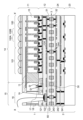
- FIG. 2 shows a schematic top view of the end portion of the semiconductor element layer 11 in Embodiment 1.
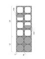
- the pixel area of the semiconductor element layer 11 includes an effective pixel area 100 in which effective pixels using incident signal charges as signals are arranged, and an optical black pixel (OB pixel) in which an optical black pixel (OB pixel) for detecting a black level reference value is arranged.
- OB pixel optical black pixel
- a black pixel region 101 is provided.
- the OB pixel region 101 is arranged around the effective pixel region 100 in a plan view, and is provided with a light blocking layer 13 that blocks light incident on the photoelectric conversion units in the OB pixel region 101 . In other words, in plan view, the OB pixel region overlaps with the light shielding region configured by the light shielding layer.
- the periphery does not have to be the entire periphery, and may be at least one of the top, bottom, left, and right of the effective pixel area 100 .
- the term “periphery” also includes what is not the entire circumference, unless otherwise specified.
- “light shielding” is not limited to blocking 100% of light. For example, it refers to something that blocks 50% or more of light.
- a well region 14 and a peripheral region 15 located around the well region 14 are arranged inside the semiconductor element layer 11 .
- the light-shielding region formed by the light-shielding layer 13 does not overlap the outer peripheral region 15 .
- the outer peripheral area 15 and the light shielding area do not completely overlap in plan view, but they may partially overlap as in an embodiment described later.
- At least a portion of pixel 10 is formed in well region 14 .
- a pad portion 16 is provided in the outer peripheral region 15 .
- the pad portion 16 is arranged between the edge of the semiconductor element layer 11 and the well region 14 .
- the shortest distance L1 between the semiconductor element layer 11 and the light shielding layer 13 is, for example, 100 ⁇ m or more and 250 ⁇ m or less, preferably 100 ⁇ m or more and 150 ⁇ m or less.
- the shortest distance L2 between the center of the pad portion 16 and the light shielding layer 13 in plan view is, for example, 30 ⁇ m or more and 200 ⁇ m or less, and preferably 50 ⁇ m or more and 100 ⁇ m or less. In order to avoid formation defects due to manufacturing errors when forming the pads, it is necessary to separate them by a predetermined distance or more.
- the center of the pad portion 16 refers to the center of the pad trench. Further, although the details will be described later, the closer the distance between the center of the pad portion 16 and the OB pixel region 101 is, the more remarkable the effect of the present embodiment is.
- the shortest distance L3 between the center of the pad portion 16 and the pixel 10 in the OB pixel region 101 is, for example, 100 ⁇ m or more and 500 ⁇ m or less, preferably 250 ⁇ m or more and 350 ⁇ m or less.
- FIG. 3 shows a schematic cross-sectional view of the X-X' cross section in FIG.
- the substrate 1 and the substrate 2 are bonded together at the bonding surface 3 and laminated.
- the wiring structure 12 of the substrate 1 and the wiring structure 24 of the substrate 2 are located.
- the wiring structure 12 has three wiring layers 121 , 122 and 123
- the wiring structure 24 has three wiring layers 241 , 242 and 243 .
- the wiring structure 12 has three wiring layers of wiring layers 121 , 122 and 123 .
- the wiring layers 121, 122, 123 can be Cu wiring layers, for example.
- the wiring layer 123 constitutes the metal portion 31 of the metal joint portion 30 .
- the metal junction 30 is embedded in a recess formed in the interlayer insulating film and has a damascene structure.
- the wiring structure 24 has three wiring layers of wiring layers 241, 242, and 243.
- the wiring layers 241, 242 and 243 may be Cu wiring layers.
- the wiring layer 243 constitutes the metal portion 32 of the metal junction portion 30 .
- the metal part 32 is embedded in a recess formed in the interlayer insulating film and has a damascene structure.
- the inter-layer insulating film having the concave portion in which the metal portion 31 is embedded, the inter-layer insulating film having the concave portion in which the metal portion 32 is embedded, and the metal portion 31 and the metal portion 32 are joined (contacted).
- the metal joint portion 30 is formed by joining the metal portion 31 and the metal portion 32 .
- the via plug 124 formed in the interlayer insulating film of the wiring layer 123 makes the metal portion 31 and the wiring layer 122 conductive.
- a via plug 244 formed in the interlayer insulating film of the wiring layer 243 electrically connects the metal portion 32 and the wiring layer 242 . Electrical connection between the semiconductor element layer 11 and the semiconductor element layer 23 is established at the metal junction 30 to which the via plugs 124 and 244 are connected.
- the wiring layer 123 includes a wiring pattern 123a connected to the wiring pattern of the upper wiring layer, and a wiring pattern 123b not connected to the wiring pattern of the upper layer.
- the wiring layer 243 includes a wiring pattern 243a connected to the underlying wiring pattern and a wiring pattern 243b not connected to the underlying wiring pattern.
- the wiring pattern 123a is connected through the via plug 124 to the upper wiring pattern.
- the wiring pattern 243a is connected to the underlying wiring pattern through the via plug 244 .
- the via plug is not essential, and the wiring pattern and the upper or lower wiring pattern may be connected by being in direct contact with each other.
- the wiring patterns 123a and 243a electrically connect the semiconductor element layer 11 and the semiconductor element layer 23 .
- the wiring patterns 123a and 243a need to connect the semiconductor element layer 11 and the semiconductor element layer 23, and some wiring patterns 123a and 243a are connected to the semiconductor element layer 11 or the semiconductor element layer 23. good too.
- some of the wiring patterns 123a and 243a may be connected to any wiring layer and may not be connected to either the semiconductor element layer 11 or the semiconductor element layer 23.
- the semiconductor element layer 11 has a well region 14 in which a well 19 is arranged, and an outer peripheral region 15 located between the edge of the semiconductor element layer 11 and the well region 14 .
- the well 19 is, for example, a region implanted with P-type impurity ions
- the peripheral region 15 is a region where the well 19 is not arranged.
- the peripheral region 15 is an N-type semiconductor region or a region having a lower P-type impurity concentration than the well 19 .
- a plurality of photoelectric conversion units in the effective pixel area 100 and a plurality of photoelectric conversion units in the OB pixel area 101 are arranged in the well 19 .
- An effective pixel region 100 and an OB pixel region 101 are arranged in the well region 14 .
- the light shielding layer 13 is arranged on the side of the light incident surface of the semiconductor element layer 11 .
- the light shielding layer is arranged on the light incident surface of the semiconductor element layer 11 via an insulating material, for example.
- a microlens is arranged on the side of the light incident surface of the semiconductor element layer 11 via an insulating material. Also, in FIG. 5, a color filter is arranged between the microlens and the insulating material.
- the arrangement of the color filters can be selected as appropriate. For example, it may be a Bayer array. Also, a plurality of photoelectric conversion units may be arranged for one microlens.
- the OB pixel area 101 is also provided with microlenses, but the microlenses are not essential. A configuration in which no microlens is arranged at a position overlapping the light shielding layer 13 in a plan view may be adopted. As shown in FIG. 3, the light shielding layer 13 may be arranged between a certain pixel 10 and an adjacent pixel 10 in a plan view in the effective pixel region 100 . Thereby, crosstalk between pixels in the effective pixel area 100 can be reduced.
- a pad portion 16 is arranged in the outer peripheral region 15 . As shown in FIG. 2 , a plurality of pad portions 16 are arranged in the outer peripheral region 15 .
- the plurality of pad portions 16 conduct electricity between the photoelectric conversion device 500 and a signal processing device or the like arranged outside the photoelectric conversion device.
- the plurality of pad sections 16 include a pad section for outputting a signal from the photoelectric conversion device 500 to the outside and a pad section for inputting a power supply voltage or the like to the photoelectric conversion device 500 .
- a trench that will become the pad section 16 is formed at the end of the semiconductor element layer 11 .
- the trench is formed in the depth direction from the light incident surface of the semiconductor element layer 11 to a depth reaching the wiring pattern of the wiring layer 242 of the substrate 2 .
- the pad portion 16 is electrically connected to the wiring layer 242 formed on the substrate 2 by wire bonding.
- the wiring layer 242 can be an Al wiring layer.
- the entire wiring layer 242 need not be made of Al, and only the wiring to which the pad section 16 is connected may be made of Al wiring, and the other wiring may be made of Cu wiring.
- a through via (TSV) in which a trench is filled with a metal may be used.
- the trench of the pad section 16 may be formed with a depth reaching the wiring layer of the substrate 1 .
- the thickness (length in the depth direction) of the semiconductor element layer 11 tends to be smaller than that of a front-illuminated photoelectric conversion device.
- the thickness of the semiconductor element layer 11 is 11 ⁇ m or less. Therefore, long-wavelength light such as infrared light incident from the light incident surface of the semiconductor element layer 11 is more likely to be reflected by the surface on which the transistor is formed and generate surplus electric charges. In particular, as shown in FIG.
- a drain portion 17 is provided for discharging surplus electric charges in the outer peripheral region 15 .
- the drain portion 17 functions as a charge discharge region for discharging surplus charges.
- a semiconductor region 171 of the same conductivity type as that of the peripheral region 15 is arranged in the drain portion 17 .
- the semiconductor region 171 can be formed by ion-implanting impurities of the same conductivity type as the peripheral region 15 .
- the semiconductor region 171 is a region with a higher impurity concentration than the peripheral region 15 .
- a contact plug 172 is formed in the semiconductor region 171 .
- a fixed potential is applied to the drain portion 17 through the wiring layer 121 and the contact plug 172 .
- the peripheral region 15 when the peripheral region 15 is N-type and the well region 14 is P-type, a positive power supply voltage is applied.
- a negative power supply voltage is applied.
- the peripheral region 15 is P-type
- ground potential is applied. Therefore, surplus electric charges can be discharged from the drain portion 17, and by creating a potential difference with the well region 14, electric charges can be prevented from being mixed into the OB pixel region 101.
- FIG. Similarly, charges generated as dark current at the edge of the substrate can also be prevented from entering the OB pixel region 101 . Therefore, it is possible to accurately detect the reference value of the black level.
- the semiconductor region 171 and the well 19 are arranged as close as possible.
- the distance between the semiconductor region 171 and the well 19 is preferably 0 ⁇ m or more and 100 ⁇ m or less. This makes it easier to suppress surplus charges such as charges photoelectrically converted near the well 19 in the peripheral region 15 and noise charges (dark current) from entering the OB pixel region 101 through the well 19 . .
- a wiring pattern common to the wiring pattern supplied to the drain of the transistor of the pixel may be used.
- the wiring pattern supplied with the VDD power of the reset transistor and the wiring pattern supplied with the VDD power supplied to the drain section 17 may be shared.
- pad portions 16 are arranged between the upper end of the semiconductor element layer 11 and the well region 14 and between the left end of the semiconductor element layer 11 and the well region 14 in plan view.
- the pad portion 16 may be arranged between the lower end of the semiconductor element layer 11 and the well region 14 and between the right end of the semiconductor element layer 11 and the well region 14 in plan view. That is, the outer peripheral region 15 in which the pad portions 16 are arranged may be arranged so as to surround the entire circumference of the well region 14 of the semiconductor element layer 11 in plan view. In such a case, the area where the light shielding layer 13 is not provided between the OB pixel region 101 and the peripheral region 15 tends to increase, so that the reference value of the black level can be detected more accurately.
- the pad portion 16 is arranged so as to surround the entire circumference of the well region 14 of the semiconductor element layer 11 in plan view. Even if the pad portion 16 is not arranged in this manner, the effects of the present invention can be obtained as long as the pad portion 16 is arranged at least partly between the end of the semiconductor element layer 11 and the well region 14 in plan view. can be obtained.
- the pad portion 16 is arranged between the upper end of the semiconductor element layer 11 and the well region 14, and the pad portion 16 is not arranged between the left end of the semiconductor element layer 11 and the well region 14. It's okay. Even in this case, it is possible to obtain the effect that the reference value of the black level can be detected more accurately.
- FIG. 4 shows a schematic top view of the edge of the semiconductor element layer 11 in the second embodiment.
- 5 shows a schematic cross-sectional view of the XX' cross section in FIG.
- the present embodiment differs from the first embodiment in that the light shielding layer 13 is arranged so as to cover the well region 14 . Since this point and points other than those described below are substantially the same as those of the first embodiment, the description thereof is omitted.
- the light shielding layer 13 is arranged so as to partially overlap the outer peripheral region 15 in plan view. That is, in a cross-sectional view, the light shielding layer 13 protrudes from the end of the well region 14 toward the pad section 16 side.
- Embodiment 1 since part of the well region 14 is not shielded from light, surplus charges photoelectrically converted in the well region 14 may enter the adjacent OB pixel region 101 .
- the well region 14 since the well region 14 is shielded from light, photoelectric conversion does not occur in the well region 14 .
- the well 19 is not exposed from the light shielding region in plan view. In other words, in plan view, the edge of the well 19 and the edge of the light shielding layer 13 are at the same position, or the edge of the light shielding layer 13 protrudes from the edge of the well 19 to the semiconductor element layer 11 side.
- FIG. 6 shows a schematic top view of the edge of the semiconductor element layer 11 in the third embodiment.
- 7 shows a schematic cross-sectional view of the XX' cross section in FIG.
- This embodiment differs from the second embodiment in that an isolation region 18 is arranged around the pad portion 16 of the semiconductor element layer 11 . Except for this point and the matters described below, since it is substantially the same as the second embodiment, the description is omitted.
- the separation region 18 is arranged so as to surround the entire circumference of the pad portion 16 in plan view.
- the isolation region 18 is an isolation region in which trenches formed in the semiconductor element layer 11 are filled with an insulating film such as a silicon oxide film or a silicon nitride film.
- the separation region 18 separates the peripheral region 15 between the vicinity of the trench of the pad portion 16 and the vicinity of the well 19 . That is, the side surface of the trench of the semiconductor element layer 11 in which the pad portion 16 is formed is insulated by the isolation region 18 from the peripheral region 15 where the drain portion 17 is arranged and the voltage is applied. Therefore, as in the second embodiment, it is possible to avoid short-circuiting between the wire bonding and the peripheral region 15 while detecting the black level reference value more accurately.
- FIG. 8 shows a schematic cross-sectional view of a stacked back-illuminated photoelectric conversion device according to the fourth embodiment.
- the semiconductor element layer 11 includes an avalanche photodiode (hereinafter referred to as APD).
- APD avalanche photodiode
- the distance L4 between the semiconductor region 161 of the second conductivity type to which the APD drive voltage is applied and the semiconductor region 171 discharging surplus charges is the distance between the well 19 and the semiconductor region 171 in the third embodiment. It differs from the third embodiment in that it is larger than . Except for these points and the points to be described below, it is substantially the same as the third embodiment, so the description is omitted.
- the APD arranged on the substrate 1 is composed of a semiconductor region 151 of a first conductivity type and a semiconductor region 152 of a second conductivity type.
- the avalanche-multiplied charge is transferred to the substrate 2 via the metal junction 30 .
- a quench circuit, a counter circuit, and the like are arranged on the substrate 2 , and a signal is sent to the counter circuit and the like of the substrate 2 through the metal joint 30 . Therefore, a metal junction 30 connecting the semiconductor element layer 11 and the semiconductor element layer 23 is arranged for each APD.
- the semiconductor region 152 of the second conductivity type In order to drive the APD, it is necessary to apply a high voltage to the semiconductor region 152 of the second conductivity type.
- the difference between the voltage applied to the semiconductor region 151 and the voltage applied to the semiconductor region 152 is, for example, 20 V or more.
- An example of the voltage applied to the semiconductor region 152 is a negative voltage with an absolute value greater than -20V.
- the voltage applied to the semiconductor region 152 is supplied from the semiconductor region 161 of the second conductivity type through the semiconductor region 153 of the second conductivity type. Therefore, the above-described high voltage is applied to the semiconductor region 161 of the second conductivity type.
- the semiconductor region 171 for discharging surplus electric charges is formed of the first conductivity type, if the semiconductor region 161 of the second conductivity type is close to the semiconductor region 161, the semiconductor region 171 and the semiconductor region 171 are separated from each other. An avalanche multiplication region is formed between. That is, there is a possibility that an avalanche multiplication region is formed in a region other than the pixel region, and surplus charges are avalanche multiplied and enter the OB pixel region 101 .
- the distance L4 between the second-conductivity-type semiconductor region 161 surrounding the pixel region and the first-conductivity-type semiconductor region 171 is set to a value such that avalanche multiplication does not occur. It should be set to distance.
- the black level reference value can be accurately detected while suppressing the formation of the avalanche multiplication region between the semiconductor regions 161 and 171. can be done.
- the distance L4 can be, for example, 1 ⁇ m or more and 10 ⁇ m or less, preferably 3 ⁇ m or more and 6 ⁇ m or less.
- the semiconductor region 171 and the light shielding layer 13 may overlap in plan view.
- FIG. 9 shows a schematic cross-sectional view of a stacked back-illuminated photoelectric conversion device according to the fifth embodiment.
- This embodiment differs from the fourth embodiment in that the drain portion 17 and the pad portion 16 are connected within the same substrate. Since this point and points other than those described below are substantially the same as those of the fourth embodiment, the description thereof is omitted.
- the trenches of the pad section 16 are formed with a depth reaching the wiring pattern of the wiring layer 122 of the substrate 1, and the wiring pattern of the wiring layer 122 is connected to the bonding wire. Then, the wiring pattern to which the bonding wire is connected and the drain portion 17 are connected via the contact plug 172 and the wiring pattern of the wiring layer 121 .
- the photoelectric conversion unit arranged on the substrate 1 is an APD
- a high voltage is required to drive the APD.
- the substrate 2 is generally formed by a fine process, it is not preferable from the standpoint of withstand voltage to apply the high voltage for driving the APD to the semiconductor element layer 23 of the substrate 2 . Therefore, it is preferable that the high voltage for driving the APD is supplied from the pads arranged on the substrate 1 . In this case, the surplus charges discharged from the drain portion 17 of the substrate 1 are discharged to the outside of the photoelectric conversion device through the pad portion 16 arranged on the substrate 1 .
- the depth of the trench of the pad portion 16 for supplying the drive voltage of the element arranged on the substrate 2 and the depth of the trench of the pad portion 16 for supplying the drive voltage of the APD arranged on the substrate 1 are different. may complicate the process and increase the difficulty of the process.
- voltages for driving the elements arranged on the substrate 2 are also applied to the pads formed on the substrate 1 and then applied to the semiconductor element layer 23 of the substrate 2 via the metal joints 40 . preferably supplied.
- the black level reference value is accurately detected while suppressing the formation of the avalanche multiplication region between the semiconductor regions 161 and 171. be able to. Moreover, since a high voltage is not applied to the semiconductor element layer 23 of the substrate 2, it becomes easier to ensure the reliability of the photoelectric conversion device when using the APD.
- FIG. 10 shows a schematic cross-sectional view of a stacked back-illuminated photoelectric conversion device according to Embodiment 6, and FIG. 1 shows a plan view.
- FIG. 11 the positions of the via plugs are also illustrated in order to make it easier to understand the positions of the via plugs in plan view.
- This embodiment is different in that the semiconductor region 161 of the second conductivity type and the light shielding layer 13 are connected via via plugs 191a, 191b, and 191c. Another difference is that color filters of different colors are arranged. Other than these points, it is substantially the same as the fifth embodiment, so the description is omitted.
- the light shielding layer 13 and the second conductivity type semiconductor region 161 are electrically connected to the via plugs 191a, 191b and 191c.
- a high voltage which is a negative voltage whose absolute value is greater than -20 V, is applied to the second conductivity type semiconductor region 161 .
- This voltage is also applied to the light shielding layer 13 through via plugs 191a, 191b, and 191c. That is, the light shielding layer 13 and the semiconductor region 161 are at the same potential. If there is a large potential difference between the semiconductor region 161 and the light shielding layer 13, there is a possibility that dielectric breakdown will occur in the insulating film interposed between the light shielding layer 13 and the semiconductor region 161. Dielectric breakdown in the film can be suppressed.
- the light shielding layer 13 and the semiconductor region 161 are connected by three via plugs in FIG. 10, they may be connected by one or two via plugs, or may be connected by four or more via plugs.
- the semiconductor region 161 is preferably arranged so as to be wider than the pixel region including the OB pixel region 101 .
- the width of the semiconductor region 161 is wider than the width of the pixel region in a cross-sectional view. This makes it easier to connect the light shielding layer 13 and the semiconductor region 161 through the via plug.
- FIG. 10 shows only one cross section, it is preferable that the width of the semiconductor region 161 is wider than the width of the pixel region 100 also in the cross section in the direction intersecting the cross section of FIG.
- the second conductivity type semiconductor region 152 forming the avalanche multiplication region of the APD may be arranged over the entire pixel region in plan view. In that case, the end portion of the second conductivity type semiconductor region 152 may be included in the second conductivity type semiconductor region 161 or may be in contact with the outer peripheral portion of the second conductivity type semiconductor region 161 . .
- the light shielding layer 13 is arranged so as to partially surround the opening of the pad section 16 in plan view.
- the light shielding layer 13 is arranged so as to surround three of the four sides forming the square in plan view.
- the light shielding layer 13 is arranged as far as the edge of the semiconductor element layer 11 as much as possible.
- via plugs 191a, 191b, and 191c are arranged so as to surround the effective pixel area 100 and the OB pixel area 101 in plan view.
- the via plugs 191a and 191b and the semiconductor region 161 are also connected in the cross section in the direction intersecting the cross section of FIG.
- the light shielding layer 13 may be arranged so as to surround the entire circumference of the pad portion 16 in plan view. As a result, the amount of light entering the semiconductor element layer 11 can be reduced more than the example shown in FIG.
- FIG. 12 does not show the via plugs 191a, 191b, and 191c shown in FIG. 11, the via plugs 191a, 191b, and 191c may be arranged. Also, an OB pixel region 101 shown in FIG. 11 may be arranged.
- the black level reference value is accurately detected while suppressing the formation of the avalanche multiplication region between the semiconductor regions 161 and 171. be able to. Moreover, since a high voltage is not applied to the semiconductor element layer 23 of the substrate 2, it becomes easier to ensure the reliability of the photoelectric conversion device when using the APD. Furthermore, dielectric breakdown of the insulating film arranged between the light shielding layer 13 and the semiconductor region 161 can be suppressed.
- FIG. 7 is an equivalent circuit diagram of a pixel in Embodiment 7
- FIGS. 14A to 14C are diagrams showing the configuration of a pixel in Embodiment 7
- FIG. 15 is a schematic top view of well region 14 in Embodiment 8.
- there is 16 shows a schematic cross-sectional view of a cross section corresponding to the XX' cross section of FIG.
- This embodiment differs from Embodiments 1 to 3 in that each pixel 10 has a plurality of photoelectric conversion units and is configured to be able to perform phase difference detection type focus detection. . Except for this point and the matters described below, the description is substantially the same as that of the other embodiments, so the description is omitted.
- FIG. 13 is a circuit diagram showing an example of a circuit of the pixels 10 arranged in two rows and one column among the pixels 10 arranged in the effective pixel area 100.
- FIG. 13 is a circuit diagram showing an example of a circuit of the pixels 10 arranged in two rows and one column among the pixels 10 arranged in the effective pixel area 100.
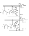
- the pixel 10 has photodiodes D1 and D2, which are photoelectric conversion units, transfer transistors M1 and M2, a charge conversion unit C1, a reset transistor M3, an amplification transistor M4, and a selection transistor M5.
- the transfer transistor M1 is provided in an electrical path between the photodiode D1 and a node to which the charge converter C1, the reset transistor M3, and the amplification transistor M4 are connected.
- the transfer transistor M2 is provided in an electrical path between the node to which the charge converter C1, the reset transistor M3, and the amplification transistor M4 are connected, and the photodiode D2.
- the charge conversion section C1 is also called a floating diffusion section (FD section).
- a power supply voltage VDD is applied to the reset transistor M3 and the amplification transistor M4.
- the selection transistor M5 is provided in an electrical path between the amplification transistor M4 and the vertical output line 50.
- FIG. It can be said that the amplification transistor M4 is electrically connected to the vertical output line 50 via the selection transistor M5.
- the charge conversion unit C1 includes a floating diffusion capacitance provided in the semiconductor substrate and a parasitic capacitance of an electrical path from the transfer transistor M1 to the amplification transistor M5 via the floating diffusion capacitance.
- Each of the signal RES, the signal Tx_A, and the signal SEL is a signal supplied from a vertical scanning circuit (not shown).
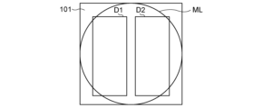
- the photodiodes D1 and D2 are arranged corresponding to one microlens ML, as shown in FIG. 14A. That is, the photodiodes D1 and D2 are arranged to receive the light transmitted through one microlens ML. Accordingly, phase difference detection type focus detection can be performed.
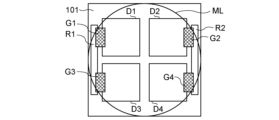
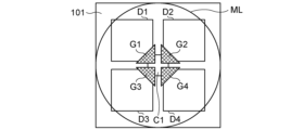
- FIGS. 14B and 14C show a configuration in which four photodiodes D1 to D4 are provided as four photoelectric conversion units for one microlens ML.
- a transfer transistor is provided corresponding to each of the photodiodes D1 to D4, and the gates G1 to G4 are gate electrodes of the corresponding transfer transistors.
- FIG. 14B gates G1, G3 transfer charge to pixel readout circuit R1.
- Gates G2 and G4 transfer charge to pixel readout circuit R2.
- Each of the pixel readout circuits R1 and R2 is provided with the capacitive element C1 shown in FIG.
- FIG. 14C shows a form in which gates G1 to G4 are provided to transfer charges to one capacitive element C1. Even in such a form, the present embodiment can be suitably implemented.
- FIG. 15 shows a schematic top view of the well region 14 in the eighth embodiment.
- the light shielding layer 13 provided on the well region 14 shields the OB pixel region 101 from light.
- the portion of the light shielding layer 13 that overlaps the effective pixel region 100 in plan view is provided with an aperture corresponding to the pixel, and light enters the corresponding pixel.
- one of the photodiodes D1 and D2 is shielded from light, and light is allowed to enter the other.
- the light-shielding layer 13 shown in FIG. 15 includes apertures corresponding to the pixels 100A having the photodiodes D2 in FIG. 14A and pixels 100B corresponding to the pixels 100B having the photodiodes D1 in FIG. 14A.
- light enters one of the photodiodes D1 and D2 for some of the pixels 10, and enters the other of the photodiodes D1 and D2 for some other pixels 10.
- phase difference detection type focus detection can be performed by reading the signals of some of the pixels 10 and some of the other pixels 10 .
- the read signal is used for focus detection by a detector provided on the second substrate, for example. Only by changing the pattern of the light shielding layer 13, pixels for phase difference detection can be formed without increasing the number of steps.
- the pixel 100A may include only one photodiode. In this case, for some of the pixels 10, part of the photodiode is shielded from light and light is allowed to enter the other part. Then, for another part of the pixels 10, a part of the photodiode at another position is shielded from light, and light is allowed to enter the other part.
- the light-shielded area is larger than that of the photodiode used for imaging.
- Focus detection can be performed by the output signal of the pixel 10 having the light-shielded photodiode.
- FIG. 16 shows a schematic cross-sectional view of a cross section corresponding to the X-X' cross section in FIG.
- the effective pixels provided in the effective pixel area 100 have pixels 100A and pixels 100B.
- the structure of the pad portion 16 is changed with respect to the cross-sectional view shown in FIG.
- the wiring structure 12 includes a first wiring layer 121 , a second wiring layer 122 and a connecting portion 31 .
- the wiring structure 24 includes a first wiring layer 242 , a second wiring layer 241 and a connecting portion 32 .
- Each wiring layer is a so-called copper wiring.
- the first wiring layer includes a conductor pattern whose main component is copper.
- the conductor pattern of the wiring layer 1 has a single damascene structure.
- a contact is provided for electrical connection between the first wiring layer and the semiconductor layer 11 .
- a contact is a conductor pattern whose main component is tungsten.
- the second wiring layer includes a conductor pattern containing copper as a main component.
- the conductor pattern of the second wiring layer has a dual damascene structure and includes portions functioning as wiring and portions functioning as vias.
- the pad electrode 60 included in the pad portion 16 is a conductor pattern whose main component is aluminum.
- the pad electrode 60 is provided in the second wiring layer of the wiring structure 12 and positioned between the first surface and the second surface of the first substrate, but the position of the pad electrode 60 is not limited to this. .
- the pad electrode 60 has a first surface and a second surface opposite to the first surface.
- the first surface is partially exposed through an opening in the semiconductor layer.
- the exposed portion of the pad electrode 60 can function as a connection portion with an external terminal, a so-called pad portion.
- the pad electrode 60 is connected on its second surface to a plurality of copper-based conductors.
- the pad electrode 60 may have a via made of a conductor mainly composed of aluminum, and may be electrically connected to a conductor mainly composed of copper located on the first surface side through the via. good. Also, the pad electrode 60 may be connected to the first wiring layer of the wiring structure 303 on the first surface by a conductor mainly composed of tungsten.
- the pad electrode 60 is formed by forming an insulator covering the wiring layer, removing a part of the insulator, forming a film mainly composed of aluminum to be the pad electrode 60, and patterning the film. can be done.
- the pad electrode 60 After forming the copper wiring, it is possible to form the pad electrode 60 having a large film thickness while maintaining the flatness of the fine copper wiring.
- the pad electrode 60 of the present embodiment is included in the wiring structure 12, it may be included in the wiring structure 24. Also, the position where the pad electrode is provided may be either of the wiring structures 121 and 122, and is not limited. The material and structure of each wiring layer of the wiring structures 121 and 122 are not limited to those illustrated, and for example, a conductor layer may be further provided between the wiring layer 1 and the semiconductor layer. Also, the contact may have a stack contact structure in which two layers are laminated.
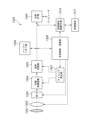
- FIG. 17 is a block diagram showing the configuration of a photoelectric conversion system 1200 according to this embodiment.
- a photoelectric conversion system 1200 of this embodiment includes a photoelectric conversion device 1204 .
- any of the photoelectric conversion devices described in the above embodiments can be applied to the photoelectric conversion device 1204 .
- the photoelectric conversion system 1200 can be used, for example, as an imaging system. Specific examples of imaging systems include digital still cameras, digital camcorders, surveillance cameras, and the like.
- FIG. 17 shows an example of a digital still camera as the photoelectric conversion system 1200 .
- a photoelectric conversion system 1200 shown in FIG. 17 includes a photoelectric conversion device 1204, a lens 1202 for forming an optical image of a subject on the photoelectric conversion device 1204, an aperture 1203 for varying the amount of light passing through the lens 1202, and protection of the lens 1202. has a barrier 1201 for A lens 1202 and a diaphragm 1203 are an optical system for condensing light onto the photoelectric conversion device 1204 .
- the photoelectric conversion system 1200 has a signal processing unit 1205 that processes the output signal output from the photoelectric conversion device 1204 .
- the signal processing unit 1205 performs a signal processing operation of performing various corrections and compressions on an input signal and outputting the signal as necessary.
- the photoelectric conversion system 1200 further includes a buffer memory section 1206 for temporarily storing image data, and an external interface section (external I/F section) 1209 for communicating with an external computer or the like.
- the photoelectric conversion system 1200 includes a recording medium 1211 such as a semiconductor memory for recording or reading image data, and a recording medium control interface section (recording medium control I/F section) for recording or reading the recording medium 1211. 1210.
- the recording medium 1211 may be built in the photoelectric conversion system 1200, or may be detachable. Communication from the recording medium control I/F unit 1210 to the recording medium 1211 and communication from the external I/F unit 1209 may be performed wirelessly.
- the photoelectric conversion system 1200 further includes an overall control/calculation unit 1208 that performs various calculations and controls the entire digital still camera, and a timing generation unit 1207 that outputs various timing signals to the photoelectric conversion device 1204 and signal processing unit 1205 .
- a timing signal or the like may be input from the outside, and the photoelectric conversion system 1200 may include at least a photoelectric conversion device 1204 and a signal processing unit 1205 that processes an output signal output from the photoelectric conversion device 1204. good.
- the timing generator 1207 may be mounted in the photoelectric conversion device as described in the fourth embodiment.
- the overall control/calculation unit 1208 and the timing generation unit 1207 may be configured to implement part or all of the control functions of the photoelectric conversion device 1204 .
- the photoelectric conversion device 1204 outputs the image signal to the signal processing unit 1205 .
- a signal processing unit 1205 performs predetermined signal processing on the image signal output from the photoelectric conversion device 1204 and outputs image data. Also, the signal processing unit 1205 generates an image using the image signal. Also, the signal processing unit 1205 may perform ranging calculation on the signal output from the photoelectric conversion device 1204 .
- the signal processing unit 1205 and the timing generation unit 1207 may be mounted on the photoelectric conversion device. That is, the signal processing unit 1205 and the timing generation unit 1207 may be provided on the substrate on which the pixels are arranged, or may be provided on another substrate.
- FIG. 18A and 18B are schematic diagrams showing configuration examples of a photoelectric conversion system and a moving object according to this embodiment.
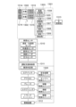
- FIG. 19 is a flowchart showing the operation of the photoelectric conversion system according to this embodiment. In this embodiment, an example of an in-vehicle camera is shown as a photoelectric conversion system.
- FIGs. 18A and 18B show an example of a vehicle system and a photoelectric conversion system mounted therein for imaging.
- a photoelectric conversion system 1301 includes a photoelectric conversion device 1302 , an image preprocessing unit 1315 , an integrated circuit 1303 and an optical system 1314 .
- An optical system 1314 forms an optical image of a subject on the photoelectric conversion device 1302 .
- the photoelectric conversion device 1302 converts the optical image of the subject formed by the optical system 1314 into an electrical signal.
- the photoelectric conversion device 1302 is the photoelectric conversion device according to any one of the embodiments described above.
- An image preprocessing unit 1315 performs predetermined signal processing on the signal output from the photoelectric conversion device 1302 .
- the functions of the image preprocessing unit 1315 may be incorporated within the photoelectric conversion device 1302 .
- the photoelectric conversion system 1301 is provided with at least two sets of an optical system 1314, a photoelectric conversion device 1302, and an image preprocessing unit 1315, and the output from each set of image preprocessing units 1315 is input to an integrated circuit 1303. It's like
- the integrated circuit 1303 is an integrated circuit for use in imaging systems, and includes an image processing unit 1304 including a memory 1305, an optical distance measurement unit 1306, a distance calculation unit 1307, an object recognition unit 1308, and an abnormality detection unit 1309.
- An image processing unit 1304 performs image processing such as development processing and defect correction on the output signal of the image preprocessing unit 1315 .
- a memory 1305 temporarily stores captured images and stores defect positions of captured pixels.
- An optical distance measurement unit 1306 performs focusing of a subject and distance measurement.
- a ranging calculation unit 1307 calculates ranging information from a plurality of image data acquired by a plurality of photoelectric conversion devices 1302 .
- the object recognition unit 1308 recognizes subjects such as cars, roads, signs, and people.
- the abnormality detection unit 1309 detects an abnormality in the photoelectric conversion device 1302, the abnormality detection unit 1309 notifies the main control unit 1313 of the abnormality.
- the integrated circuit 1303 may be realized by specially designed hardware, software modules, or a combination thereof. Also, it may be realized by FPGA (Field Programmable Gate Array), ASIC (Application Specific Integrated Circuit), etc., or by a combination thereof.
- FPGA Field Programmable Gate Array
- ASIC Application Specific Integrated Circuit
- the main control unit 1313 integrates and controls the operations of the photoelectric conversion system 1301, the vehicle sensor 1310, the control unit 1320, and the like. There is also a method in which the photoelectric conversion system 1301, the vehicle sensor 1310, and the control unit 1320 have individual communication interfaces without having the main control unit 1313, and each of them transmits and receives control signals via a communication network (for example, CAN standard).
- a communication network for example, CAN standard
- the integrated circuit 1303 has a function of receiving a control signal from the main control unit 1313 or transmitting a control signal and setting values to the photoelectric conversion device 1302 by its own control unit.
- the photoelectric conversion system 1301 is connected to a vehicle sensor 1310, and can detect the running state of the own vehicle such as vehicle speed, yaw rate, and steering angle, the environment outside the own vehicle, and the state of other vehicles and obstacles.
- the vehicle sensor 1310 also serves as distance information acquisition means for acquiring distance information to an object.
- the photoelectric conversion system 1301 is also connected to a driving support control unit 1311 that performs various driving support functions such as automatic steering, automatic cruise, and anti-collision functions.
- the collision determination function based on the detection results of the photoelectric conversion system 1301 and the vehicle sensor 1310, it is possible to estimate a collision with another vehicle/obstacle and determine whether or not there is a collision. As a result, avoidance control when a collision is presumed and safety device activation at the time of collision are performed.
- the photoelectric conversion system 1301 is also connected to an alarm device 1312 that issues an alarm to the driver based on the judgment result of the collision judgment section. For example, if the judgment result of the collision judging section indicates that the possibility of collision is high, the main control section 1313 controls the vehicle to avoid collision and reduce damage by applying the brakes, releasing the accelerator, or suppressing the engine output. conduct.
- the alarm device 1312 warns the user by sounding an alarm such as sound, displaying alarm information on a display unit screen of a car navigation system or a meter panel, or vibrating a seat belt or steering wheel.
- the photoelectric conversion system 1301 photographs the surroundings of the vehicle, for example, the front or rear.
- FIG. 18B shows an arrangement example of the photoelectric conversion system 1301 when the photoelectric conversion system 1301 captures an image in front of the vehicle.
- the two photoelectric conversion devices 1302 are arranged in front of the vehicle 1300 . Specifically, if the center line of the vehicle 1300 with respect to the direction of movement or the outer shape (for example, the width of the vehicle) is regarded as the axis of symmetry, and the two photoelectric conversion devices 1302 are arranged line-symmetrically with respect to the axis of symmetry, the vehicle 1300 and This is preferable for obtaining information on the distance to the object to be photographed and for determining the possibility of collision. Moreover, the photoelectric conversion device 1302 is preferably arranged so as not to obstruct the driver's field of vision when the driver visually recognizes the situation outside the vehicle 1300 from the driver's seat. It is preferable that the warning device 1312 be arranged so as to be easily visible to the driver.
- the failure detection operation of photoelectric conversion device 1302 in the photoelectric conversion system 1301 will be described using FIG.
- the failure detection operation of photoelectric conversion device 1302 is performed according to steps S1410 to S1480 shown in FIG.
- Step S1410 is a step for performing settings at startup of the photoelectric conversion device 1302 . That is, the settings for the operation of the photoelectric conversion device 1302 are transmitted from outside the photoelectric conversion system 1301 (for example, the main control unit 1313) or inside the photoelectric conversion system 1301, and the imaging operation and failure detection operation of the photoelectric conversion device 1302 are performed. Start.
- step S1420 pixel signals are obtained from effective pixels. Also, in step S1430, an output value is obtained from a failure detection pixel provided for failure detection.
- This failure detection pixel has a photoelectric conversion section like the effective pixel. A predetermined voltage is written in the photoelectric conversion unit. The failure detection pixel outputs a signal corresponding to the voltage written to the photoelectric conversion section. Note that steps S1420 and S1430 may be reversed.
- step S1440 it is determined whether the expected output value of the failure-detected pixel and the actual output value from the failure-detected pixel match.
- step S1450 it is determined that the imaging operation is performed normally, and the processing step proceeds to step S1460. and migrate.
- step S1460 the pixel signals of the scanning line are transmitted to the memory 1305 for temporary storage. After that, the process returns to step S1420 to continue the failure detection operation.
- the process proceeds to step S1470.
- step S1470 it is determined that there is an abnormality in the imaging operation, and an alarm is issued to the main control unit 1313 or the alarm device 1312.
- FIG. The alarm device 1312 causes the display unit to display that an abnormality has been detected.
- step S1480 the photoelectric conversion device 1302 is stopped, and the operation of the photoelectric conversion system 1301 ends.
- step S1470 may be notified to the outside of the vehicle via a wireless network.
- the control that does not collide with another vehicle has been described, but it is also applicable to control that automatically drives following another vehicle, control that automatically drives so as not to stray from the lane, and the like.
- the photoelectric conversion system 1301 can be applied not only to a vehicle such as a vehicle, but also to a moving object (moving device) such as a ship, an aircraft, or an industrial robot.
- the present invention can be applied not only to mobile objects but also to devices that widely use object recognition, such as intelligent transportation systems (ITS).
- ITS intelligent transportation systems
- the photoelectric conversion device of the present invention may further have a configuration capable of acquiring various information such as distance information.
Abstract
This photoelectric conversion device comprises: a first substrate having a first semiconductor element layer including a plurality of photoelectric conversion parts and a well in which the plurality of photoelectric conversion parts are arranged; and a second substrate having a second semiconductor element layer including a circuit for processing signals acquired by the plurality of photoelectric conversion parts. The first substrate and the second substrate are stacked. The first semiconductor element layer has: an effective pixel region; an OB pixel region provided between the effective pixel region and an edge of the first semiconductor element layer; and a peripheral region arranged between the OB pixel region and the edge of the first semiconductor element layer. The effective pixel region is such that, in a plan view of one of the plurality of photoelectric conversion parts that has a greater light-shielded area than the other photoelectric conversion parts, a light-shielding region constituted by a light-shielding layer overlaps the OB pixel region and does not overlap the peripheral region. The peripheral region includes a charge draining region including a semiconductor region of the same conductivity type as a signal charge. A fixed potential is supplied to the charge draining region.
Description
本発明は、光電変換装置、光電変換システム、および移動体に関する。
The present invention relates to a photoelectric conversion device, a photoelectric conversion system, and a moving body.
複数の画素を含む有効画素領域と、有効画素領域の周りに配され遮光されたオプティカル・ブラック(OB)領域と、を有する光電変換装置が知られている。特許文献1には、裏面照射型の光電変換装置が開示されている。半導体基板において、配線層が配される側の面とは反対の面から光が照射される裏面照射型の光電変換装置が開示されている。特許文献1では、有効画素領域とOB領域との間、または、OB領域とに、有効画素領域から漏れてくる信号電荷を排出する電荷排出画素が、有効画素領域とOB領域との間に配されている。そして、有効画素領域から漏れてくる信号電荷を強制的に排出している。
A photoelectric conversion device is known that has an effective pixel area including a plurality of pixels and an optical black (OB) area arranged around the effective pixel area and shielded from light. Patent Literature 1 discloses a back-illuminated photoelectric conversion device. 2. Description of the Related Art A back-illuminated photoelectric conversion device is disclosed in which light is irradiated from a surface of a semiconductor substrate opposite to a surface on which a wiring layer is arranged. In Japanese Patent Application Laid-Open No. 2004-100000, charge discharging pixels for discharging signal charges leaking from the effective pixel region are arranged between the effective pixel region and the OB region, or in the OB region. It is Then, signal charges leaking from the effective pixel area are forcibly discharged.
特許文献1は、有効画素領域からOB領域に混入する余剰電荷については考察されているが、OB領域の周囲からOB領域に混入する余剰電荷については考察されていない。つまり、特許文献1のように基板の端部にOB画素が配置される場合には、OB領域の周囲で生じた信号電荷がOB領域へと混入すると、黒レベルの基準信号が変動するため、OB領域への余剰電荷の混入も抑制する必要がある。特に、積層型の光電変換装置の場合には、画素から出力される信号を処理する信号処理回路をOB領域の周囲に配置する必要がなくなるため、本発明の効果がより顕著となる。
Although Patent Document 1 considers the surplus charge that enters the OB region from the effective pixel region, it does not consider the surplus charge that enters the OB region from the periphery of the OB region. That is, when OB pixels are arranged at the edge of the substrate as in Patent Document 1, when signal charges generated around the OB region are mixed into the OB region, the reference signal of the black level fluctuates. It is also necessary to suppress mixing of surplus charges into the OB region. In particular, in the case of a stacked photoelectric conversion device, there is no need to dispose a signal processing circuit for processing signals output from pixels around the OB region, so the effect of the present invention becomes more pronounced.
また、特許文献1には、通行画素領域に配された複数の光電変換部のうち、他の光電変換部よりも遮光された面積が大きい光電変換部を含む場合に関する考察は為されていない。
In addition, Patent Document 1 does not discuss the case where, among the plurality of photoelectric conversion units arranged in the passing pixel area, a photoelectric conversion unit having a larger shielded area than other photoelectric conversion units is included.
本発明は、積層型の光電変換装置において、OB領域への余剰電荷の混入を抑制し、黒レベルの基準信号の検出をより正確に行うことが可能な光電変換装置を提供することを目的とする。
SUMMARY OF THE INVENTION It is an object of the present invention to provide a stacked photoelectric conversion device capable of suppressing the mixture of surplus electric charges in the OB region and more accurately detecting a black level reference signal. do.
本開示の一の側面は、複数の光電変換部と、前記複数の光電変換部が配されるウェルと、を含む第1半導体素子層を有する第1基板と、前記複数の光電変換部で得られた信号を処理する回路を含む第2半導体素子層を有する第2基板と、を備え、前記第1基板と前記第2基板とは積層されており、前記第1半導体素子層は、前記複数の光電変換部を有する有効画素領域と、前記有効画素領域と前記第1半導体素子の端との間に設けられ、前記複数の光電変換部を有するオプティカル・ブラック画素領域と、前記オプティカル・ブラック画素領域と前記第1半導体素子層の端との間に配された外周領域と、を有し、前記有効画素領域は、前記複数の光電変換部のうち、他の光電変換部よりも遮光された面積が大きい光電変換部を含み、平面視で、前記オプティカル・ブラック画素領域には、遮光層で構成される遮光領域が重複しており、前記外周領域には前記遮光領域が重複しておらず、前記外周領域には、信号電荷と同じ導電型の半導体領域を含む電荷排出領域があり、前記電荷排出領域には、固定電位が供給されていることを特徴とする光電変換装置である。
According to one aspect of the present disclosure, a first substrate having a first semiconductor element layer including a plurality of photoelectric conversion units and a well in which the plurality of photoelectric conversion units are arranged; a second substrate having a second semiconductor element layer including a circuit for processing the received signal, wherein the first substrate and the second substrate are laminated, and the first semiconductor element layer includes the plurality of an effective pixel region having a photoelectric conversion portion of; an optical black pixel region provided between the effective pixel region and an end of the first semiconductor element and having the plurality of photoelectric conversion portions; and the optical black pixel and a peripheral region arranged between the region and an edge of the first semiconductor element layer, wherein the effective pixel region is shielded from light more than the other photoelectric conversion units among the plurality of photoelectric conversion units. Including a photoelectric conversion portion having a large area, in a plan view, the optical black pixel region overlaps with a light shielding region constituted by a light shielding layer, and the outer peripheral region does not overlap with the light shielding region. and a charge discharge region including a semiconductor region of the same conductivity type as that of signal charges is provided in the peripheral region, and a fixed potential is supplied to the charge discharge region.
本発明によれば、OB領域への余剰電荷の混入を抑制し、黒レベルの基準信号の検出をより正確に行うことが可能な積層型の光電変換装置を提供することが可能となる。
According to the present invention, it is possible to provide a stacked photoelectric conversion device capable of suppressing the mixture of surplus electric charges in the OB region and more accurately detecting the reference signal of the black level.
以下に示す形態は、本発明の技術思想を具体化するためのものであって、本発明を限定するものではない。各図面が示す部材の大きさや位置関係は、説明を明確にするために誇張していることがある。以下の説明において、同一の構成については同一の番号を付して説明を省略することがある。
The form shown below is for embodying the technical idea of the present invention, and does not limit the present invention. The sizes and positional relationships of members shown in each drawing may be exaggerated for clarity of explanation. In the following description, the same configuration may be assigned the same number and the description thereof may be omitted.
以下の説明において、信号電荷と同じ導電型のキャリアを多数キャリアとする第1導電型の半導体領域とはN型半導体領域であり、第2導電型の半導体領域とはP型半導体領域である。なお、信号電荷がホールである場合でも本発明は成立する。この場合は、信号電荷と同じ導電型のキャリアを多数キャリアとする第1導電型の半導体領域はP型半導体領域であり、第2導電型の半導体領域とはN型半導体領域である。
In the following description, the semiconductor region of the first conductivity type having majority carriers of the same conductivity type as the signal charges is the N-type semiconductor region, and the semiconductor region of the second conductivity type is the P-type semiconductor region. Note that the present invention is established even when the signal charges are holes. In this case, the semiconductor region of the first conductivity type having majority carriers of the same conductivity type as the signal charges is a P-type semiconductor region, and the semiconductor region of the second conductivity type is an N-type semiconductor region.
本明細書および請求項において、単に「不純物濃度」という用語が使われた場合、逆導電型の不純物によって補償された正味の不純物濃度を意味している。つまり、「不純物濃度」とは、NETドーピング濃度を指す。P型の添加不純物濃度がN型の添加不純物濃度より高い領域はP型半導体領域である。反対に、N型の添加不純物濃度がP型の添加不純物濃度より高い領域はN型半導体領域である。
In the present specification and claims, when the term "impurity concentration" is simply used, it means the net impurity concentration compensated for by impurities of the opposite conductivity type. In other words, "impurity concentration" refers to NET doping concentration. A region in which the P-type impurity concentration is higher than the N-type impurity concentration is a P-type semiconductor region. On the contrary, a region where the N-type impurity concentration is higher than the P-type impurity concentration is an N-type semiconductor region.
本明細書において、「平面視」とは、後述する半導体基板の光入射面に対して垂直な方向から視ることを指す。また、断面とは、半導体基板の光入射面と垂直な方向における面を指す。なお、微視的に見て半導体基板の光入射面が粗面である場合は、巨視的に見たときの半導体基板の光入射面を基準として平面視を定義する。
In this specification, "planar view" refers to viewing from a direction perpendicular to a light incident surface of a semiconductor substrate, which will be described later. Moreover, the cross section refers to a plane in a direction perpendicular to the light incident surface of the semiconductor substrate. When the light incident surface of the semiconductor substrate is microscopically rough, the plane view is defined with reference to the light incident surface of the semiconductor substrate macroscopically.
本明細書において、深さ方向は、半導体基板の光入射面(第1面)からトランジスタが配される側の面(第2面)に向かう方向である。
In this specification, the depth direction is the direction from the light incident surface (first surface) of the semiconductor substrate toward the surface (second surface) on which the transistors are arranged.
(実施形態1)
図1は、実施形態1に係る光電変換装置500を示している。光電変換装置は、半導体デバイスICである。本実施形態に係る光電変換装置500とは、例えば、イメージセンサや、測光センサ、測距センサとして用いることができる。 (Embodiment 1)
FIG. 1 shows aphotoelectric conversion device 500 according to the first embodiment. A photoelectric conversion device is a semiconductor device IC. The photoelectric conversion device 500 according to this embodiment can be used as, for example, an image sensor, a photometry sensor, or a distance measurement sensor.
図1は、実施形態1に係る光電変換装置500を示している。光電変換装置は、半導体デバイスICである。本実施形態に係る光電変換装置500とは、例えば、イメージセンサや、測光センサ、測距センサとして用いることができる。 (Embodiment 1)
FIG. 1 shows a
光電変換装置500は、基板1と基板2との全部または一部が、積層して接合された積層型の光電変換装置である。基板1および基板2は、積層後にウェハをダイシングしてチップ化したチップの状態であってもよいし、ウェハの状態であってもよい。光電変換装置500は、積層型の裏面照射型の光電変換装置である。
The photoelectric conversion device 500 is a laminated photoelectric conversion device in which all or part of the substrate 1 and the substrate 2 are laminated and joined. The substrates 1 and 2 may be in the state of chips obtained by dicing the wafer after lamination, or may be in the state of wafers. The photoelectric conversion device 500 is a stacked back-illuminated photoelectric conversion device.
基板1は、画素10に含まれる画素回路を含む半導体素子層11(第1半導体素子層)と、配線構造12(第1配線構造)と、を有する。本明細書において、「半導体素子層」とは、半導体層のみではなく、半導体層と半導体層に形成されたトランジスタのゲートとを含む。配線構造の配線層は「半導体素子層」に含まれない。基板2は、配線構造24(第2配線構造)と、電気回路を含む半導体素子層23(第2半導体素子層)と、を有する。後述するが、基板1の配線構造12と基板2の配線構造24とは、各配線構造に含まれる配線層を接合することで構成された金属接合部により接合されている。金属接合部とは、配線層を構成する金属と配線層を構成する金属とが直接接合された構造である。
The substrate 1 has a semiconductor element layer 11 (first semiconductor element layer) including pixel circuits included in the pixels 10, and a wiring structure 12 (first wiring structure). In this specification, the term "semiconductor element layer" includes not only a semiconductor layer but also a semiconductor layer and a gate of a transistor formed in the semiconductor layer. The wiring layer of the wiring structure is not included in the "semiconductor element layer". The substrate 2 has a wiring structure 24 (second wiring structure) and a semiconductor element layer 23 (second semiconductor element layer) including an electric circuit. As will be described later, the wiring structure 12 of the substrate 1 and the wiring structure 24 of the substrate 2 are joined by a metal joint formed by joining the wiring layers included in each wiring structure. A metal joint portion is a structure in which a metal forming a wiring layer and a metal forming a wiring layer are directly joined.
詳細は後述するが、画素10を構成する素子は、半導体素子層11に配される。なお、画素10の一部の構成が半導体素子層11に配され、他の一部の構成が半導体素子層に配されてもよい。この場合、画素10のうちの半導体素子層11に配される画素回路の構成としては、フォトダイオードなどの光電変換素子が挙げられる。光電変換素子を含む画素回路は、半導体素子層11に平面視で2次元アレイ状に配される。半導体素子層11は、複数の画素回路が2次元アレイ状に配された画素領域を有する。図1では、半導体素子層11には、複数の画素回路を構成する複数の光電変換素子が行方向および列方向の2次元アレイ状に配されている。
Although the details will be described later, the elements forming the pixels 10 are arranged in the semiconductor element layer 11 . A part of the structure of the pixel 10 may be arranged in the semiconductor element layer 11 and the other part of the structure may be arranged in the semiconductor element layer. In this case, the configuration of the pixel circuit arranged in the semiconductor element layer 11 of the pixel 10 includes a photoelectric conversion element such as a photodiode. Pixel circuits including photoelectric conversion elements are arranged in a two-dimensional array on the semiconductor element layer 11 in plan view. The semiconductor element layer 11 has a pixel region in which a plurality of pixel circuits are arranged in a two-dimensional array. In FIG. 1, the semiconductor element layer 11 has a plurality of photoelectric conversion elements forming a plurality of pixel circuits arranged in a two-dimensional array in row and column directions.
配線構造12は、M(Mは1以上の整数)層の配線層と層間絶縁材料を含む。配線構造24は、N(Nは1以上の整数)層の配線層と層間絶縁材料を含む。
The wiring structure 12 includes M (M is an integer equal to or greater than 1) wiring layers and an interlayer insulating material. The wiring structure 24 includes N (N is an integer equal to or greater than 1) wiring layers and an interlayer insulating material.
半導体素子層23は、半導体素子層11に配された光電変換部で得られた信号を処理する電気回路を含む。説明の便宜上、図1において、基板2の上面に図示された構成は半導体素子層23に配された構成である。電気回路とは、例えば、図1に示す、行走査回路20、列走査回路21、信号処理回路22等を構成するトランジスタのいずれか1つである。信号処理回路22とは、例えば、増幅トランジスタ、選択トランジスタ、リセットトランジスタなどの画素10の構成の一部、増幅回路、選択回路、論理演算回路、AD変換回路、メモリ、圧縮処理や合成処理等を行う回路の少なくともいずれか1つである。
The semiconductor element layer 23 includes an electric circuit that processes signals obtained by the photoelectric conversion units arranged in the semiconductor element layer 11 . For convenience of explanation, the configuration shown on the upper surface of the substrate 2 in FIG. The electric circuit is, for example, any one of the transistors constituting the row scanning circuit 20, the column scanning circuit 21, the signal processing circuit 22, etc. shown in FIG. The signal processing circuit 22 includes, for example, a part of the configuration of the pixel 10 such as an amplification transistor, a selection transistor, and a reset transistor, an amplification circuit, a selection circuit, a logical operation circuit, an AD conversion circuit, a memory, compression processing, synthesis processing, and the like. at least one of the circuits that
画素10は、画像を構成するために繰り返して配置される回路の最小単位を指しうる。そして、画素10に含まれ、半導体素子層11に配された画素回路は、少なくとも、光電変換素子を含んでいればよい。画素回路には、光電変換素子以外の構成を含んでいてもよい。例えば、画素回路はさらに、転送トランジスタ、FD、リセットトランジスタ、増幅トランジスタ、容量付加トランジスタ、選択トランジスタの少なくともいずれか1つを含んでいてもよい。典型的には、選択トランジスタ及び当該選択トランジスタを介して信号線に接続された一群の素子が画素10を構成する。すなわち、選択トランジスタが画素回路の外縁でありうる。あるいは、光電変換素子と転送トランジスタの組が画素10を構成することもある。他にも、1つあるいは複数の光電変換素子と、1つの増幅回路あるいは1つのAD変換回路との組が画素10を構成してもよい。
A pixel 10 can refer to the smallest circuit unit that is repeatedly arranged to form an image. A pixel circuit included in the pixel 10 and arranged on the semiconductor element layer 11 may include at least a photoelectric conversion element. The pixel circuit may include components other than the photoelectric conversion element. For example, the pixel circuit may further include at least one of a transfer transistor, FD, reset transistor, amplification transistor, capacitance addition transistor, and selection transistor. Typically, a pixel 10 is composed of a selection transistor and a group of elements connected to a signal line via the selection transistor. That is, the selection transistor can be the outer edge of the pixel circuit. Alternatively, the pixel 10 may be composed of a set of a photoelectric conversion element and a transfer transistor. Alternatively, the pixel 10 may be composed of a set of one or more photoelectric conversion elements and one amplifier circuit or one AD conversion circuit.
図2は、実施形態1における半導体素子層11の端部における上面模式図を示している。半導体素子層11の画素領域は、入射した信号電荷を信号として用いる有効画素が配された有効画素領域100と、黒レベルの基準値を検出するオプティカル・ブラック画素(OB画素)が配されたオプティカル・ブラック画素領域101とが設けられている。OB画素領域101は、平面視で、有効画素領域100の周囲に配置され、OB画素領域101内の光電変換部へ入射する光を遮光する遮光層13が設けられている。言い換えると、平面視で、OB画素領域には、遮光層で構成される遮光領域が重複する。周囲とは全周である必要はなく、有効画素領域100の上下左右の少なくともいずれかどこかであればよい。以下においても、「周囲」といった場合には、特に説明する場合を除き、全周ではないものも含まれる。また、「遮光」とは光を100%遮るものに限定されない。例えば、光を50%以上遮るものを指す。
FIG. 2 shows a schematic top view of the end portion of the semiconductor element layer 11 in Embodiment 1. FIG. The pixel area of the semiconductor element layer 11 includes an effective pixel area 100 in which effective pixels using incident signal charges as signals are arranged, and an optical black pixel (OB pixel) in which an optical black pixel (OB pixel) for detecting a black level reference value is arranged. - A black pixel region 101 is provided. The OB pixel region 101 is arranged around the effective pixel region 100 in a plan view, and is provided with a light blocking layer 13 that blocks light incident on the photoelectric conversion units in the OB pixel region 101 . In other words, in plan view, the OB pixel region overlaps with the light shielding region configured by the light shielding layer. The periphery does not have to be the entire periphery, and may be at least one of the top, bottom, left, and right of the effective pixel area 100 . In the following description, the term "periphery" also includes what is not the entire circumference, unless otherwise specified. Also, "light shielding" is not limited to blocking 100% of light. For example, it refers to something that blocks 50% or more of light.
半導体素子層11の内部には、ウェル領域14と、ウェル領域14の周囲に位置する外周領域15と、が配される。平面視で、外周領域15には、遮光層13で構成される遮光領域が重複しない。本実施形態では、外周領域15と遮光領域とが平面視で完全に重複しないが、後述する実施形態のように一部が重複していてもよい。画素10の少なくとも一部はウェル領域14の中に形成されている。外周領域15には、パッド部16が設けられている。
A well region 14 and a peripheral region 15 located around the well region 14 are arranged inside the semiconductor element layer 11 . In plan view, the light-shielding region formed by the light-shielding layer 13 does not overlap the outer peripheral region 15 . In this embodiment, the outer peripheral area 15 and the light shielding area do not completely overlap in plan view, but they may partially overlap as in an embodiment described later. At least a portion of pixel 10 is formed in well region 14 . A pad portion 16 is provided in the outer peripheral region 15 .
パッド部16は、半導体素子層11の端と、ウェル領域14との間に配されている。平面視で、半導体素子層11と遮光層13との最短距離L1は、例えば、100μm以上250μm以下であり、100μm以上150μm以下であることが好ましい。また、例えば、平面視で、パッド部16の中心と遮光層13との最短距離L2は、例えば、30μm以上200μm以下であり、50μm以上100μm以下であることが好ましい。パッド部形成時の製造誤差による形成不良を回避するためには、所定以上の距離を離す必要がある。一方で、半導体素子層11の面積を広げることなく有効画素領域100の面積を広げるために所定以下の距離とすることが好ましい。パッド部16の中心とは、パッドのトレンチの中心を指す。また、詳細は後述するが、パッド部16の中心とOB画素領域101との距離が近いほど、本実施形態の効果はより顕著となる。パッド部16の中心とOB画素領域101の画素10との最短距離L3は、例えば、100μm以上500μm以下であり、250μm以上350μm以下であることが好ましい。
The pad portion 16 is arranged between the edge of the semiconductor element layer 11 and the well region 14 . In plan view, the shortest distance L1 between the semiconductor element layer 11 and the light shielding layer 13 is, for example, 100 μm or more and 250 μm or less, preferably 100 μm or more and 150 μm or less. Further, for example, the shortest distance L2 between the center of the pad portion 16 and the light shielding layer 13 in plan view is, for example, 30 μm or more and 200 μm or less, and preferably 50 μm or more and 100 μm or less. In order to avoid formation defects due to manufacturing errors when forming the pads, it is necessary to separate them by a predetermined distance or more. On the other hand, in order to increase the area of the effective pixel region 100 without increasing the area of the semiconductor element layer 11, it is preferable to set the distance to a predetermined value or less. The center of the pad portion 16 refers to the center of the pad trench. Further, although the details will be described later, the closer the distance between the center of the pad portion 16 and the OB pixel region 101 is, the more remarkable the effect of the present embodiment is. The shortest distance L3 between the center of the pad portion 16 and the pixel 10 in the OB pixel region 101 is, for example, 100 μm or more and 500 μm or less, preferably 250 μm or more and 350 μm or less.
図3は、図2におけるX-X’断面の断面模式図を示している。基板1と基板2は、接合面3で貼り合されて積層されている。基板1の半導体素子層11と基板2の半導体素子層23との間には、基板1の配線構造12と基板2の配線構造24が位置している。図3では、配線構造12は、配線層121、122、123の3層の配線層を有し、配線構造24は、配線層241、242、243の3層の配線層を有する。
FIG. 3 shows a schematic cross-sectional view of the X-X' cross section in FIG. The substrate 1 and the substrate 2 are bonded together at the bonding surface 3 and laminated. Between the semiconductor element layer 11 of the substrate 1 and the semiconductor element layer 23 of the substrate 2, the wiring structure 12 of the substrate 1 and the wiring structure 24 of the substrate 2 are located. In FIG. 3 , the wiring structure 12 has three wiring layers 121 , 122 and 123 , and the wiring structure 24 has three wiring layers 241 , 242 and 243 .
配線構造12は、配線層121、122、123の3層の配線層を有している。配線層121、122、123は例えば、Cu配線層でありうる。図3では、配線層123が金属接合部30のメタル部31を構成する。金属接合部30は層間絶縁膜に形成された凹部に埋め込まれ、ダマシン構造を有している。
The wiring structure 12 has three wiring layers of wiring layers 121 , 122 and 123 . The wiring layers 121, 122, 123 can be Cu wiring layers, for example. In FIG. 3 , the wiring layer 123 constitutes the metal portion 31 of the metal joint portion 30 . The metal junction 30 is embedded in a recess formed in the interlayer insulating film and has a damascene structure.
配線構造24は配線層241、242、243の3層の配線層を有している。配線層241、242、243はCu配線層でありうる。図3では、配線層243が金属接合部30のメタル部32を構成する。メタル部32は層間絶縁膜に形成された凹部に埋め込まれ、ダマシン構造を有している。
The wiring structure 24 has three wiring layers of wiring layers 241, 242, and 243. The wiring layers 241, 242 and 243 may be Cu wiring layers. In FIG. 3 , the wiring layer 243 constitutes the metal portion 32 of the metal junction portion 30 . The metal part 32 is embedded in a recess formed in the interlayer insulating film and has a damascene structure.
メタル部31が埋め込まれた凹部を有する層間絶縁膜と、メタル部32が埋め込まれた凹部を有する層間絶縁膜と、メタル部31、メタル部32とにより接合(接触)している。メタル部31とメタル部32とが接合されることにより、金属接合部30が形成される。
The inter-layer insulating film having the concave portion in which the metal portion 31 is embedded, the inter-layer insulating film having the concave portion in which the metal portion 32 is embedded, and the metal portion 31 and the metal portion 32 are joined (contacted). The metal joint portion 30 is formed by joining the metal portion 31 and the metal portion 32 .
ここで、配線層123の層間絶縁膜中に形成されたビアプラグ124はメタル部31と配線層122とを導電させる。配線層243の層間絶縁膜中に形成されたビアプラグ244はメタル部32と配線層242とを導電させる。ビアプラグ124及び244が接続される金属接合部30で半導体素子層11と半導体素子層23との電気的な接続を行っている。
Here, the via plug 124 formed in the interlayer insulating film of the wiring layer 123 makes the metal portion 31 and the wiring layer 122 conductive. A via plug 244 formed in the interlayer insulating film of the wiring layer 243 electrically connects the metal portion 32 and the wiring layer 242 . Electrical connection between the semiconductor element layer 11 and the semiconductor element layer 23 is established at the metal junction 30 to which the via plugs 124 and 244 are connected.
例えば、配線層123は、その上層の配線層の配線パターンと接続された配線パターン123aと、その上層の配線パターンとは接続されていない配線パターン123bとを含む。また、配線層243は、その下層の配線パターンと接続された243aと、その下層の配線パターンとは接続されていない配線パターン243bとを含む。例えば、図3では、配線パターン123aは、ビアプラグ124を介して、その上層の配線パターンと接続されている。また、配線パターン243aは、ビアプラグ244を介してその下層の配線パターンと接続されている。なお、ビアプラグは必須ではなく、配線パターンと上層又は下層の配線パターンとが直接接することにより接続されていてもよい。
For example, the wiring layer 123 includes a wiring pattern 123a connected to the wiring pattern of the upper wiring layer, and a wiring pattern 123b not connected to the wiring pattern of the upper layer. Further, the wiring layer 243 includes a wiring pattern 243a connected to the underlying wiring pattern and a wiring pattern 243b not connected to the underlying wiring pattern. For example, in FIG. 3, the wiring pattern 123a is connected through the via plug 124 to the upper wiring pattern. Also, the wiring pattern 243a is connected to the underlying wiring pattern through the via plug 244 . The via plug is not essential, and the wiring pattern and the upper or lower wiring pattern may be connected by being in direct contact with each other.
図3では、配線パターン123a、243aとは半導体素子層11および半導体素子層23を電気的に接続している。なお、すべての配線パターン123a、243aが、半導体素子層11および半導体素子層23を接続する必要はなく、一部の配線パターン123a、243aが半導体素子層11または半導体素子層23に接続されていてもよい。また、一部の配線パターン123a、243aが、いずれかの配線層まで接続され、半導体素子層11および半導体素子層23のいずれにも接続されていなくてもよい。
In FIG. 3, the wiring patterns 123a and 243a electrically connect the semiconductor element layer 11 and the semiconductor element layer 23 . Note that not all the wiring patterns 123a and 243a need to connect the semiconductor element layer 11 and the semiconductor element layer 23, and some wiring patterns 123a and 243a are connected to the semiconductor element layer 11 or the semiconductor element layer 23. good too. Also, some of the wiring patterns 123a and 243a may be connected to any wiring layer and may not be connected to either the semiconductor element layer 11 or the semiconductor element layer 23. FIG.
図3に示すように、半導体素子層11は、ウェル19が配されたウェル領域14と、半導体素子層11の端とウェル領域14との間に位置する外周領域15とを有する。ウェル19は、例えば、P型の不純物がイオン注入された領域であり、外周領域15は、ウェル19が配されていない領域である。外周領域15は、N型半導体領域、または、ウェル19よりもP型の不純物濃度が低い領域である。
As shown in FIG. 3, the semiconductor element layer 11 has a well region 14 in which a well 19 is arranged, and an outer peripheral region 15 located between the edge of the semiconductor element layer 11 and the well region 14 . The well 19 is, for example, a region implanted with P-type impurity ions, and the peripheral region 15 is a region where the well 19 is not arranged. The peripheral region 15 is an N-type semiconductor region or a region having a lower P-type impurity concentration than the well 19 .
ウェル19には、有効画素領域100の複数の光電変換部と、OB画素領域101の複数の光電変換部とが配される。ウェル領域14には、有効画素領域100と、OB画素領域101とが配されている。OB画素領域101には、半導体素子層11の光入射面の側に遮光層13が配される。遮光層は、例えば、絶縁材料を介して半導体素子層11の光入射面に配される。半導体素子層11の光入射面の側には、絶縁材料を介して、マイクロレンズが配される。また、図5において、マイクロレンズと絶縁材料との間には、カラーフィルタが配される。カラーフィルタの配置は適宜選択することができる。例えば、ベイヤー配列であってもよい。また、1つのマイクロレンズに対して複数の光電変換部が配されていてもよい。図3では、OB画素領域101にもマイクロレンズが配されるが、マイクロレンズは必須ではない。遮光層13と平面視で重なる位置には、マイクロレンズを配さない構成としてもよい。図3に示すように、遮光層13は、有効画素領域100において、平面視で、ある画素10と隣り合う画素10との間に配されてもよい。これにより、有効画素領域100における画素間のクロストークを低減することができる。
A plurality of photoelectric conversion units in the effective pixel area 100 and a plurality of photoelectric conversion units in the OB pixel area 101 are arranged in the well 19 . An effective pixel region 100 and an OB pixel region 101 are arranged in the well region 14 . In the OB pixel region 101 , the light shielding layer 13 is arranged on the side of the light incident surface of the semiconductor element layer 11 . The light shielding layer is arranged on the light incident surface of the semiconductor element layer 11 via an insulating material, for example. A microlens is arranged on the side of the light incident surface of the semiconductor element layer 11 via an insulating material. Also, in FIG. 5, a color filter is arranged between the microlens and the insulating material. The arrangement of the color filters can be selected as appropriate. For example, it may be a Bayer array. Also, a plurality of photoelectric conversion units may be arranged for one microlens. In FIG. 3, the OB pixel area 101 is also provided with microlenses, but the microlenses are not essential. A configuration in which no microlens is arranged at a position overlapping the light shielding layer 13 in a plan view may be adopted. As shown in FIG. 3, the light shielding layer 13 may be arranged between a certain pixel 10 and an adjacent pixel 10 in a plan view in the effective pixel region 100 . Thereby, crosstalk between pixels in the effective pixel area 100 can be reduced.
外周領域15には、パッド部16が配される。図2に示すように、外周領域15には、複数のパッド部16が配される。複数のパッド部16は、光電変換装置500と光電変換装置の外部に配された信号処理装置などとの通電を行う。複数のパッド部16には、光電変換装置500からの信号を外部に出力するパッド部や、光電変換装置500に電源電圧などを入力するパッド部が含まれる。
A pad portion 16 is arranged in the outer peripheral region 15 . As shown in FIG. 2 , a plurality of pad portions 16 are arranged in the outer peripheral region 15 . The plurality of pad portions 16 conduct electricity between the photoelectric conversion device 500 and a signal processing device or the like arranged outside the photoelectric conversion device. The plurality of pad sections 16 include a pad section for outputting a signal from the photoelectric conversion device 500 to the outside and a pad section for inputting a power supply voltage or the like to the photoelectric conversion device 500 .
図3に示すように、半導体素子層11の端部には、パッド部16となるトレンチが形成される。トレンチは、半導体素子層11の光入射面から深さ方向に形成され、基板2の配線層242の配線パターンに達する深さまで形成される。パッド部16において、基板2に形成された配線層242にワイヤーボンディングで導通されている。
As shown in FIG. 3, a trench that will become the pad section 16 is formed at the end of the semiconductor element layer 11 . The trench is formed in the depth direction from the light incident surface of the semiconductor element layer 11 to a depth reaching the wiring pattern of the wiring layer 242 of the substrate 2 . The pad portion 16 is electrically connected to the wiring layer 242 formed on the substrate 2 by wire bonding.
配線層242はAl配線層でありうる。なお、配線層242の全体がAlである必要はなく、パッド部16が接続される配線のみをAl配線とし、その他の配線はCu配線としてもよい。ここではワイヤーボンディングの例を示したが、トレンチ内に金属が充填された貫通ビア(TSV)であっても良い。
The wiring layer 242 can be an Al wiring layer. The entire wiring layer 242 need not be made of Al, and only the wiring to which the pad section 16 is connected may be made of Al wiring, and the other wiring may be made of Cu wiring. Although an example of wire bonding is shown here, a through via (TSV) in which a trench is filled with a metal may be used.
なお、パッド部16のトレンチは、基板1の配線層に達する深さで形成されていてもよい。
Note that the trench of the pad section 16 may be formed with a depth reaching the wiring layer of the substrate 1 .
上述の通り、パッド部16はトレンチを形成する必要があるため、遮光層13を近接まで設けることができない。裏面照射型の光電変換装置の場合は、半導体素子層11の厚み(深さ方向における長さ)が、表面入射型の光電変換装置に比べて小さくなりやすい。例えば、半導体素子層11の厚みは、11μm以下となる。したがって、半導体素子層11の光入射面から入射した赤外光などの長波長の光が、トランジスタが形成される側の面で反射されて余剰電荷が発生する可能性が高くなる。特に、図3に示すように、基板1に走査回路や信号処理回路などの周辺回路が搭載されていない積層型の裏面照射型の光電変換装置の構成では、基板の端とOB画素領域101との距離が近くなる。言い換えると、積層型の裏面照射型の光電変換装置の構成では、パッド部16とウェル19との間には、回路素子が配されていない。そのため、ウェル領域14の一部や外周領域15などの非遮光領域に光が入射すると光電変換されて電荷が生成されることがありうる。非遮光領域で生成された余剰電荷がウェル領域14を介してOB画素領域101に混入すると、黒レベルの基準値の検出が不正確となり、有効画素領域の画素値を正しく補正することができない。
As described above, since it is necessary to form a trench in the pad section 16, the light shielding layer 13 cannot be provided close to it. In the case of a back-illuminated photoelectric conversion device, the thickness (length in the depth direction) of the semiconductor element layer 11 tends to be smaller than that of a front-illuminated photoelectric conversion device. For example, the thickness of the semiconductor element layer 11 is 11 μm or less. Therefore, long-wavelength light such as infrared light incident from the light incident surface of the semiconductor element layer 11 is more likely to be reflected by the surface on which the transistor is formed and generate surplus electric charges. In particular, as shown in FIG. 3, in the configuration of the laminated backside illumination type photoelectric conversion device in which peripheral circuits such as a scanning circuit and a signal processing circuit are not mounted on the substrate 1, the edge of the substrate and the OB pixel region 101 are separated from each other. becomes closer. In other words, no circuit element is arranged between the pad section 16 and the well 19 in the structure of the stacked backside illumination photoelectric conversion device. Therefore, when light enters a non-light-shielding region such as part of the well region 14 or the peripheral region 15, it may be photoelectrically converted to generate charges. If surplus charges generated in the non-light-shielded area enter the OB pixel area 101 through the well area 14, detection of the reference value of the black level becomes inaccurate, and pixel values in the effective pixel area cannot be correctly corrected.
本実施形態では、外周領域15において余剰電荷を排出するドレイン部17が設けられている。ドレイン部17は、余剰電荷を排出する電荷排出領域として機能する。ドレイン部17には外周領域15と同じ導電型の半導体領域171が配されている。半導体領域171は、外周領域15と同じ導電型の不純物をイオン注入することにより形成することができる。半導体領域171は、外周領域15よりも不純物濃度の高い領域である。また半導体領域171にはコンタクトプラグ172が形成されている。ドレイン部17には配線層121及びコンタクトプラグ172を介して固定電位が印加されている。例えば外周領域15がN型でウェル領域14がP型の場合は、正電位の電源電圧が印加されている。また、外周領域15がP型でウェル領域14がN型の場合は、負電位の電源電圧が印加されている。例えば、外周領域15がP型の場合には、グラウンド電位が印加される。そのためドレイン部17では余剰電荷を排出することができ、ウェル領域14との間に電位差をつけることで、OB画素領域101への電荷の混入を抑制することがでる。また同様に、基板の端で暗電流として生成された電荷も、OB画素領域101へ混入すること抑制することがでる。そのため黒レベルの基準値の検出を正確に行うことができる。
In this embodiment, a drain portion 17 is provided for discharging surplus electric charges in the outer peripheral region 15 . The drain portion 17 functions as a charge discharge region for discharging surplus charges. A semiconductor region 171 of the same conductivity type as that of the peripheral region 15 is arranged in the drain portion 17 . The semiconductor region 171 can be formed by ion-implanting impurities of the same conductivity type as the peripheral region 15 . The semiconductor region 171 is a region with a higher impurity concentration than the peripheral region 15 . A contact plug 172 is formed in the semiconductor region 171 . A fixed potential is applied to the drain portion 17 through the wiring layer 121 and the contact plug 172 . For example, when the peripheral region 15 is N-type and the well region 14 is P-type, a positive power supply voltage is applied. When the peripheral region 15 is P-type and the well region 14 is N-type, a negative power supply voltage is applied. For example, if the peripheral region 15 is P-type, ground potential is applied. Therefore, surplus electric charges can be discharged from the drain portion 17, and by creating a potential difference with the well region 14, electric charges can be prevented from being mixed into the OB pixel region 101. FIG. Similarly, charges generated as dark current at the edge of the substrate can also be prevented from entering the OB pixel region 101 . Therefore, it is possible to accurately detect the reference value of the black level.
半導体領域171とウェル19とはできるだけ近づけて配することが好ましい。例えば、半導体領域171とウェル19との間の距離は、0μm以上100μm以下であることが好ましい。これにより、外周領域15のうちのウェル19の近傍で光電変換された電荷やノイズ電荷(暗電流)などの余剰電荷が、ウェル19を通ってOB画素領域101に混入することを抑制しやすくなる。
It is preferable to arrange the semiconductor region 171 and the well 19 as close as possible. For example, the distance between the semiconductor region 171 and the well 19 is preferably 0 μm or more and 100 μm or less. This makes it easier to suppress surplus charges such as charges photoelectrically converted near the well 19 in the peripheral region 15 and noise charges (dark current) from entering the OB pixel region 101 through the well 19 . .
ドレイン部17に接続される配線層121の配線パターンは、画素のトランジスタのドレインに供給される配線パターンと共通の配線パターンを用いてもよい。例えば、リセットトランジスタのVDD電源が供給される配線パターンと、ドレイン部17に供給されるVDD電源が供給される配線パターンとを共通にしてもよい。
For the wiring pattern of the wiring layer 121 connected to the drain portion 17, a wiring pattern common to the wiring pattern supplied to the drain of the transistor of the pixel may be used. For example, the wiring pattern supplied with the VDD power of the reset transistor and the wiring pattern supplied with the VDD power supplied to the drain section 17 may be shared.
なお、図2では、平面視で半導体素子層11の上端とウェル領域14との間、および、半導体素子層11の左端とウェル領域14との間にパッド部16が配されている。パッド部16は、平面視で半導体素子層11の下端とウェル領域14との間、および、半導体素子層11の右端とウェル領域14との間に配されていてもよい。つまり、平面視で、半導体素子層11のウェル領域14の全周を取り囲むように、パッド部16が配された外周領域15が配されていてもよい。このような場合は、OB画素領域101と外周領域15との間に遮光層13が配されない領域ができる面積が大きくなりやすいため、黒レベルの基準値の検出をより正確に行うことができるという効果を顕著に得ることができる。なお、平面視で半導体素子層11のウェル領域14の全周を取り囲むようにパッド部16が配されていることは必須ではない。このようにパッド部16が配されていない場合でも、平面視で、半導体素子層11の端とウェル領域14との間の少なくとも一部にパッド部16が配されていれば、本発明の効果を得ることができる。例えば、平面視で半導体素子層11の上端とウェル領域14との間にパッド部16が配され、半導体素子層11の左端とウェル領域14との間にはパッド部16が配されていない形態でもよい。この場合でも、黒レベルの基準値の検出をより正確に行うことができるという効果を得ることは可能である。
Note that in FIG. 2, pad portions 16 are arranged between the upper end of the semiconductor element layer 11 and the well region 14 and between the left end of the semiconductor element layer 11 and the well region 14 in plan view. The pad portion 16 may be arranged between the lower end of the semiconductor element layer 11 and the well region 14 and between the right end of the semiconductor element layer 11 and the well region 14 in plan view. That is, the outer peripheral region 15 in which the pad portions 16 are arranged may be arranged so as to surround the entire circumference of the well region 14 of the semiconductor element layer 11 in plan view. In such a case, the area where the light shielding layer 13 is not provided between the OB pixel region 101 and the peripheral region 15 tends to increase, so that the reference value of the black level can be detected more accurately. Remarkable effect can be obtained. Note that it is not essential that the pad portion 16 is arranged so as to surround the entire circumference of the well region 14 of the semiconductor element layer 11 in plan view. Even if the pad portion 16 is not arranged in this manner, the effects of the present invention can be obtained as long as the pad portion 16 is arranged at least partly between the end of the semiconductor element layer 11 and the well region 14 in plan view. can be obtained. For example, in a plan view, the pad portion 16 is arranged between the upper end of the semiconductor element layer 11 and the well region 14, and the pad portion 16 is not arranged between the left end of the semiconductor element layer 11 and the well region 14. It's okay. Even in this case, it is possible to obtain the effect that the reference value of the black level can be detected more accurately.
(実施形態2)
図4は、実施形態2における半導体素子層11の端部における上面模式図を示している。また図5は、図4におけるX-X’断面の断面模式図を示している。本実施形態は、遮光層13がウェル領域14を覆うように配置されている点が実施形態1とは異なる。この点および以下で説明する点以外は、実施形態1と実質的に同じであるため説明を省略する。 (Embodiment 2)
FIG. 4 shows a schematic top view of the edge of thesemiconductor element layer 11 in the second embodiment. 5 shows a schematic cross-sectional view of the XX' cross section in FIG. The present embodiment differs from the first embodiment in that the light shielding layer 13 is arranged so as to cover the well region 14 . Since this point and points other than those described below are substantially the same as those of the first embodiment, the description thereof is omitted.
図4は、実施形態2における半導体素子層11の端部における上面模式図を示している。また図5は、図4におけるX-X’断面の断面模式図を示している。本実施形態は、遮光層13がウェル領域14を覆うように配置されている点が実施形態1とは異なる。この点および以下で説明する点以外は、実施形態1と実質的に同じであるため説明を省略する。 (Embodiment 2)
FIG. 4 shows a schematic top view of the edge of the
図5に示すように、本実施形態では平面視で遮光層13が外周領域15と部分的に重なるように配されている。つまり、断面視において、遮光層13がウェル領域14の端からパッド部16の側へと突き出ている。
As shown in FIG. 5, in this embodiment, the light shielding layer 13 is arranged so as to partially overlap the outer peripheral region 15 in plan view. That is, in a cross-sectional view, the light shielding layer 13 protrudes from the end of the well region 14 toward the pad section 16 side.
実施形態1の場合では、ウェル領域14の一部が遮光されていないために、ウェル領域14で光電変換された余剰電荷が近接するOB画素領域101への混入する可能性がある。一方で、実施形態2では、ウェル領域14が遮光されているため、ウェル領域14では光電変換されない。言い換えると、平面視でウェル19は遮光領域から露出しない。つまり、平面視で、ウェル19の端と遮光層13の端とが同じ位置、または、ウェル19の端よりも遮光層13の端が半導体素子層11の側まで突き出ている。このような場合は、半導体素子層11の端部での余剰電荷の生成は非遮光領域の外周領域15のみとなる。外周領域15にはドレイン部17が設けられているため余剰電荷が排出されるため、実施形態1に対してOB画素領域101への電荷の混入をより抑制することができる。そのため黒レベルの基準値の検出をより正確に行うことができる。
In the case of Embodiment 1, since part of the well region 14 is not shielded from light, surplus charges photoelectrically converted in the well region 14 may enter the adjacent OB pixel region 101 . On the other hand, in the second embodiment, since the well region 14 is shielded from light, photoelectric conversion does not occur in the well region 14 . In other words, the well 19 is not exposed from the light shielding region in plan view. In other words, in plan view, the edge of the well 19 and the edge of the light shielding layer 13 are at the same position, or the edge of the light shielding layer 13 protrudes from the edge of the well 19 to the semiconductor element layer 11 side. In such a case, surplus charges are generated only in the peripheral region 15 of the non-light-shielding region at the edge of the semiconductor element layer 11 . Since the drain portion 17 is provided in the outer peripheral region 15, surplus electric charges are discharged. Therefore, the black level reference value can be detected more accurately.
(実施形態3)
図6は、実施形態3における半導体素子層11の端部における上面模式図を示している。また図7は、図6におけるX-X’断面の断面模式図を示している。本実施形態は、半導体素子層11のパッド部16の周りに分離領域18が配置されている点が実施形態2とは異なる。この点および以下で説明する事項以外は、実施形態2と実質的に同じであるため説明を省略する。 (Embodiment 3)
FIG. 6 shows a schematic top view of the edge of thesemiconductor element layer 11 in the third embodiment. 7 shows a schematic cross-sectional view of the XX' cross section in FIG. This embodiment differs from the second embodiment in that an isolation region 18 is arranged around the pad portion 16 of the semiconductor element layer 11 . Except for this point and the matters described below, since it is substantially the same as the second embodiment, the description is omitted.
図6は、実施形態3における半導体素子層11の端部における上面模式図を示している。また図7は、図6におけるX-X’断面の断面模式図を示している。本実施形態は、半導体素子層11のパッド部16の周りに分離領域18が配置されている点が実施形態2とは異なる。この点および以下で説明する事項以外は、実施形態2と実質的に同じであるため説明を省略する。 (Embodiment 3)
FIG. 6 shows a schematic top view of the edge of the
分離領域18は、平面視で、パッド部16の全周を取り囲むように配されている。分離領域18は、半導体素子層11内に形成されたトレンチの中に、シリコン酸化膜もしくはシリコン窒化膜などの絶縁膜が埋め込まれた素子分離である。
The separation region 18 is arranged so as to surround the entire circumference of the pad portion 16 in plan view. The isolation region 18 is an isolation region in which trenches formed in the semiconductor element layer 11 are filled with an insulating film such as a silicon oxide film or a silicon nitride film.
実施形態2の場合は、パッド部16が形成された半導体素子層11のパッド部16のトレンチの側面にワイヤーボンディングが接触すると、電圧印加された外周領域15とショートしてしまう。一方で、実施形態3の場合は、分離領域18により、外周領域15をパッド部16のトレンチの近傍と、ウェル19の近傍とで分離している。つまり、パッド部16が形成された半導体素子層11のトレンチの側面が、ドレイン部17が配され、電圧印加される外周領域15から分離領域18で絶縁される。そのため、実施形態2と同様に、黒レベルの基準値の検出をより正確に行いながら、ワイヤーボンディングと外周領域15とのショートを回避することができる。
In the case of the second embodiment, when wire bonding contacts the side surface of the trench of the pad portion 16 of the semiconductor element layer 11 on which the pad portion 16 is formed, it short-circuits with the peripheral region 15 to which the voltage is applied. On the other hand, in the case of the third embodiment, the separation region 18 separates the peripheral region 15 between the vicinity of the trench of the pad portion 16 and the vicinity of the well 19 . That is, the side surface of the trench of the semiconductor element layer 11 in which the pad portion 16 is formed is insulated by the isolation region 18 from the peripheral region 15 where the drain portion 17 is arranged and the voltage is applied. Therefore, as in the second embodiment, it is possible to avoid short-circuiting between the wire bonding and the peripheral region 15 while detecting the black level reference value more accurately.
(実施形態4)
図8は、実施形態4における積層型の裏面照射型の光電変換装置における断面模式図を示している。本実施形態は、半導体素子層11がアバランシェフォトダイオード(以下、APD)を含む点が異なる。また、APD駆動電圧が印加される第2導電型の半導体領域161と、余剰電荷を排出する半導体領域171との間の距離L4が、実施形態3におけるウェル19と半導体領域171との間の距離よりも大きい点が実施形態3とは異なる。これらの点および以下で説明する点以外は、実施形態3と実質的に同じであるため説明を省略する。 (Embodiment 4)
FIG. 8 shows a schematic cross-sectional view of a stacked back-illuminated photoelectric conversion device according to the fourth embodiment. This embodiment is different in that thesemiconductor element layer 11 includes an avalanche photodiode (hereinafter referred to as APD). In addition, the distance L4 between the semiconductor region 161 of the second conductivity type to which the APD drive voltage is applied and the semiconductor region 171 discharging surplus charges is the distance between the well 19 and the semiconductor region 171 in the third embodiment. It differs from the third embodiment in that it is larger than . Except for these points and the points to be described below, it is substantially the same as the third embodiment, so the description is omitted.
図8は、実施形態4における積層型の裏面照射型の光電変換装置における断面模式図を示している。本実施形態は、半導体素子層11がアバランシェフォトダイオード(以下、APD)を含む点が異なる。また、APD駆動電圧が印加される第2導電型の半導体領域161と、余剰電荷を排出する半導体領域171との間の距離L4が、実施形態3におけるウェル19と半導体領域171との間の距離よりも大きい点が実施形態3とは異なる。これらの点および以下で説明する点以外は、実施形態3と実質的に同じであるため説明を省略する。 (Embodiment 4)
FIG. 8 shows a schematic cross-sectional view of a stacked back-illuminated photoelectric conversion device according to the fourth embodiment. This embodiment is different in that the
基板1に配置するAPDは、第1導電型の半導体領域151と、第2導電型の半導体領域152で構成される。アバランシェ増倍された電荷は、金属接合部30を介して基板2へ送られる。基板2には、クエンチ回路や、カウンタ回路等が配されており、金属接合部30を介して基板2のカウンタ回路等に信号が送られる。したがって、APDごとに半導体素子層11と半導体素子層23とを接続する金属接合部30が配されている。
The APD arranged on the substrate 1 is composed of a semiconductor region 151 of a first conductivity type and a semiconductor region 152 of a second conductivity type. The avalanche-multiplied charge is transferred to the substrate 2 via the metal junction 30 . A quench circuit, a counter circuit, and the like are arranged on the substrate 2 , and a signal is sent to the counter circuit and the like of the substrate 2 through the metal joint 30 . Therefore, a metal junction 30 connecting the semiconductor element layer 11 and the semiconductor element layer 23 is arranged for each APD.
APDを駆動するためには、第2導電型の半導体領域152に高電圧を印加する必要がある。半導体領域151への印加電圧と半導体領域152への印加電圧との差は、例えば、20V以上である。半導体領域152への印加電圧の一例としては、―20Vより絶対値が大きい負電圧である。半導体領域152への印加電圧は、第2導電型の半導体領域161から第2導電型の半導体領域153を介して供給される。従って、第2導電型の半導体領域161には、前述した高電圧が印加される。
In order to drive the APD, it is necessary to apply a high voltage to the semiconductor region 152 of the second conductivity type. The difference between the voltage applied to the semiconductor region 151 and the voltage applied to the semiconductor region 152 is, for example, 20 V or more. An example of the voltage applied to the semiconductor region 152 is a negative voltage with an absolute value greater than -20V. The voltage applied to the semiconductor region 152 is supplied from the semiconductor region 161 of the second conductivity type through the semiconductor region 153 of the second conductivity type. Therefore, the above-described high voltage is applied to the semiconductor region 161 of the second conductivity type.
一方で、余剰電荷を排出するための半導体領域171は第1導電型で形成されるため、第2導電型の半導体領域161との間が近接していると、半導体領域161と半導体領域171との間でアバランシェ増倍領域が形成される。つまり、画素領域以外の領域でアバランシェ増倍領域が形成され、余剰電荷がアバランシェ増倍されてOB画素領域101へと入射する可能性がある。
On the other hand, since the semiconductor region 171 for discharging surplus electric charges is formed of the first conductivity type, if the semiconductor region 161 of the second conductivity type is close to the semiconductor region 161, the semiconductor region 171 and the semiconductor region 171 are separated from each other. An avalanche multiplication region is formed between. That is, there is a possibility that an avalanche multiplication region is formed in a region other than the pixel region, and surplus charges are avalanche multiplied and enter the OB pixel region 101 .
したがって、基板1に配置する光電変換部がAPDの場合、画素領域を取り囲む第2導電型の半導体領域161と、第1導電型の半導体領域171の距離L4を、アバランシェ増倍が起きないような距離に設定する必要がある。
Therefore, when the photoelectric conversion unit arranged on the substrate 1 is an APD, the distance L4 between the second-conductivity-type semiconductor region 161 surrounding the pixel region and the first-conductivity-type semiconductor region 171 is set to a value such that avalanche multiplication does not occur. It should be set to distance.
本実施形態によれば、距離L4を離間させているため、半導体領域161と半導体領域171との間でアバランシェ増倍領域が形成されることを抑制しながら、黒レベルの基準値の検出を正確に行うことができる。
According to this embodiment, since the distance L4 is set apart, the black level reference value can be accurately detected while suppressing the formation of the avalanche multiplication region between the semiconductor regions 161 and 171. can be done.
距離L4は、例えば、1μm以上10μm以下とすることができ、3μm以上6μm以下とすることが好ましい。
The distance L4 can be, for example, 1 μm or more and 10 μm or less, preferably 3 μm or more and 6 μm or less.
図8に示すように平面視で、半導体領域171と遮光層13とが重なっていてもよい。
As shown in FIG. 8, the semiconductor region 171 and the light shielding layer 13 may overlap in plan view.
(実施形態5)
図9は、実施形態5における積層型の裏面照射型の光電変換装置における断面模式図を示している。本実施形態は、ドレイン部17がパッド部16と同一基板内で接続される点が実施形態4とは異なる。この点および以下で説明する点以外は、実施形態4と実質的に同じであるため説明を省略する。 (Embodiment 5)
FIG. 9 shows a schematic cross-sectional view of a stacked back-illuminated photoelectric conversion device according to the fifth embodiment. This embodiment differs from the fourth embodiment in that thedrain portion 17 and the pad portion 16 are connected within the same substrate. Since this point and points other than those described below are substantially the same as those of the fourth embodiment, the description thereof is omitted.
図9は、実施形態5における積層型の裏面照射型の光電変換装置における断面模式図を示している。本実施形態は、ドレイン部17がパッド部16と同一基板内で接続される点が実施形態4とは異なる。この点および以下で説明する点以外は、実施形態4と実質的に同じであるため説明を省略する。 (Embodiment 5)
FIG. 9 shows a schematic cross-sectional view of a stacked back-illuminated photoelectric conversion device according to the fifth embodiment. This embodiment differs from the fourth embodiment in that the
本実施形態では、パッド部16のトレンチが基板1の配線層122の配線パターンに達する深さで形成されており、配線層122の配線パターンがボンディングワイヤと接続されている。そして、ボンディングワイヤが接続される配線パターンとドレイン部17が、コンタクトプラグ172および配線層121の配線パターンを介して接続される。
In this embodiment, the trenches of the pad section 16 are formed with a depth reaching the wiring pattern of the wiring layer 122 of the substrate 1, and the wiring pattern of the wiring layer 122 is connected to the bonding wire. Then, the wiring pattern to which the bonding wire is connected and the drain portion 17 are connected via the contact plug 172 and the wiring pattern of the wiring layer 121 .
実施形態4で説明のとおり、基板1に配置する光電変換部がAPDの場合、APDを駆動させるために高電圧が必要になる。一方で、基板2は一般的に微細プロセスで形成されるため、前記のようなAPD駆動用の高電圧を基板2の半導体素子層23に印加することは、耐圧の観点から好ましくない。従って、APD駆動用の高電圧は基板1に配置されるパッドから供給されることが好ましい。この場合は、基板1のドレイン部17から排出された余剰電荷は、基板1に配置されるパッド部16を介して光電変換装置の外部へと排出される。
As described in Embodiment 4, when the photoelectric conversion unit arranged on the substrate 1 is an APD, a high voltage is required to drive the APD. On the other hand, since the substrate 2 is generally formed by a fine process, it is not preferable from the standpoint of withstand voltage to apply the high voltage for driving the APD to the semiconductor element layer 23 of the substrate 2 . Therefore, it is preferable that the high voltage for driving the APD is supplied from the pads arranged on the substrate 1 . In this case, the surplus charges discharged from the drain portion 17 of the substrate 1 are discharged to the outside of the photoelectric conversion device through the pad portion 16 arranged on the substrate 1 .
また、基板2に配される素子の駆動用電圧を供給するパッド部16のトレンチの深さと、基板1に配されるAPDの駆動用電圧を供給するパッド部16のトレンチの深さとが異なる場合は、工程が複雑になりプロセス上の難易度が高まる場合がある。
Further, when the depth of the trench of the pad portion 16 for supplying the drive voltage of the element arranged on the substrate 2 and the depth of the trench of the pad portion 16 for supplying the drive voltage of the APD arranged on the substrate 1 are different. may complicate the process and increase the difficulty of the process.
したがって、本実施形態では、基板2に配置される素子を駆動するための電圧も、基板1に形成されたパッドに印加した上で、金属接合部40を介して基板2の半導体素子層23に供給することが好ましい。
Therefore, in the present embodiment, voltages for driving the elements arranged on the substrate 2 are also applied to the pads formed on the substrate 1 and then applied to the semiconductor element layer 23 of the substrate 2 via the metal joints 40 . preferably supplied.
本実施形態によれば、実施形態4と同様に、半導体領域161と半導体領域171との間でアバランシェ増倍領域が形成されることを抑制しながら、黒レベルの基準値の検出を正確に行うことができる。また、高電圧が基板2の半導体素子層23に印加されないため、APDを用いる場合の光電変換装置の信頼性を確保しやすくなる。
According to the present embodiment, similarly to the fourth embodiment, the black level reference value is accurately detected while suppressing the formation of the avalanche multiplication region between the semiconductor regions 161 and 171. be able to. Moreover, since a high voltage is not applied to the semiconductor element layer 23 of the substrate 2, it becomes easier to ensure the reliability of the photoelectric conversion device when using the APD.
(実施形態6)
図10は、実施形態6における積層型の裏面照射型の光電変換装置における断面模式図を示しており、図11は、実施形態6における光電変換装置の光入射面側から視た遮光層の概略平面図を示している。図11では、平面視でのビアプラグの位置をわかりやすくするために、ビアプラグの位置も図示している。本実施形態は、第2導電型の半導体領域161と遮光層13とがビアプラグ191a、191b、191cを介して接続されている点が異なる。また、異なる色のカラーフィルタが配されている点が異なる。これらの点以外は、実施形態5と実質的に同じであるため説明を省略する。 (Embodiment 6)
FIG. 10 shows a schematic cross-sectional view of a stacked back-illuminated photoelectric conversion device according to Embodiment 6, and FIG. 1 shows a plan view. In FIG. 11, the positions of the via plugs are also illustrated in order to make it easier to understand the positions of the via plugs in plan view. This embodiment is different in that thesemiconductor region 161 of the second conductivity type and the light shielding layer 13 are connected via via plugs 191a, 191b, and 191c. Another difference is that color filters of different colors are arranged. Other than these points, it is substantially the same as the fifth embodiment, so the description is omitted.
図10は、実施形態6における積層型の裏面照射型の光電変換装置における断面模式図を示しており、図11は、実施形態6における光電変換装置の光入射面側から視た遮光層の概略平面図を示している。図11では、平面視でのビアプラグの位置をわかりやすくするために、ビアプラグの位置も図示している。本実施形態は、第2導電型の半導体領域161と遮光層13とがビアプラグ191a、191b、191cを介して接続されている点が異なる。また、異なる色のカラーフィルタが配されている点が異なる。これらの点以外は、実施形態5と実質的に同じであるため説明を省略する。 (Embodiment 6)
FIG. 10 shows a schematic cross-sectional view of a stacked back-illuminated photoelectric conversion device according to Embodiment 6, and FIG. 1 shows a plan view. In FIG. 11, the positions of the via plugs are also illustrated in order to make it easier to understand the positions of the via plugs in plan view. This embodiment is different in that the
図10に示すように、遮光層13と、第2導電型の半導体領域161とは、ビアプラグ191a、191b、191cと導通している。実施形態4で説明したように、第2導電型の半導体領域161には、―20Vより絶対値が大きい負電圧である高電圧が印加される。そして、この電圧がビアプラグ191a、191b、191cを介して遮光層13にも印加されている。つまり、遮光層13と半導体領域161とは同電位となっている。半導体領域161と遮光層13との電位差が多い気場合は、遮光層13と半導体領域161との間に配された絶縁膜で絶縁破壊が生じる可能性があるところ、本実施形態によれば絶縁膜での絶縁破壊を抑制することができる。
As shown in FIG. 10, the light shielding layer 13 and the second conductivity type semiconductor region 161 are electrically connected to the via plugs 191a, 191b and 191c. As described in the fourth embodiment, a high voltage, which is a negative voltage whose absolute value is greater than -20 V, is applied to the second conductivity type semiconductor region 161 . This voltage is also applied to the light shielding layer 13 through via plugs 191a, 191b, and 191c. That is, the light shielding layer 13 and the semiconductor region 161 are at the same potential. If there is a large potential difference between the semiconductor region 161 and the light shielding layer 13, there is a possibility that dielectric breakdown will occur in the insulating film interposed between the light shielding layer 13 and the semiconductor region 161. Dielectric breakdown in the film can be suppressed.
図10では、3つのビアプラグにより遮光層13と半導体領域161とを接続しているが、1つまたは2つのビアプラグで接続してもよいし、4つ以上のビアプラグで接続してもよい。
Although the light shielding layer 13 and the semiconductor region 161 are connected by three via plugs in FIG. 10, they may be connected by one or two via plugs, or may be connected by four or more via plugs.
図10に示すように、半導体領域161は、OB画素領域101を含む画素領域よりも幅が広くなるように配されることが好ましい。つまり、断面視で、画素領域の幅よりも、半導体領域161の幅が広くなるように配置されることが好ましい。これにより、ビアプラグを介して遮光層13と半導体領域161とを接続しやすくなる。図10では、一断面のみ示しているが、図10の断面と交差する方向における断面においても、画素領域100の幅よりも半導体領域161の幅が広くなるように配置されることが好ましい。
As shown in FIG. 10, the semiconductor region 161 is preferably arranged so as to be wider than the pixel region including the OB pixel region 101 . In other words, it is preferable that the width of the semiconductor region 161 is wider than the width of the pixel region in a cross-sectional view. This makes it easier to connect the light shielding layer 13 and the semiconductor region 161 through the via plug. Although FIG. 10 shows only one cross section, it is preferable that the width of the semiconductor region 161 is wider than the width of the pixel region 100 also in the cross section in the direction intersecting the cross section of FIG.
APDのアバランシェ増倍領域を形成する第2導電型の半導体領域152は、平面視で画素領域全面に配置されていてもよい。その場合、第2導電型の半導体領域152の端部は、第2導電型の半導体領域161に内包されていてもよいし、第2導電型の半導体領域161の外周部と接していてもよい。
The second conductivity type semiconductor region 152 forming the avalanche multiplication region of the APD may be arranged over the entire pixel region in plan view. In that case, the end portion of the second conductivity type semiconductor region 152 may be included in the second conductivity type semiconductor region 161 or may be in contact with the outer peripheral portion of the second conductivity type semiconductor region 161 . .
図11では、遮光層13は、平面視でパッド部16の開口を部分的に囲むように配置している。例えば、開口が四角形の場合に、平面視で四角形を構成する4辺のうちの3辺を囲むように遮光層13が配置されている。このように、遮光層13はできるだけ半導体素子層11の端まで配置されることが好ましい。
In FIG. 11, the light shielding layer 13 is arranged so as to partially surround the opening of the pad section 16 in plan view. For example, when the opening is a square, the light shielding layer 13 is arranged so as to surround three of the four sides forming the square in plan view. Thus, it is preferable that the light shielding layer 13 is arranged as far as the edge of the semiconductor element layer 11 as much as possible.
図11に示すように、有効画素領域100およびOB画素領域101を平面視で取り囲むようにビアプラグ191a、191b、191cが配置されている。そして、図10の断面と交差する方向における断面においても、ビアプラグ191a、191bと半導体領域161が接続されている。このように、有効画素領域100およびOB画素領域101の全周を取り囲むように、ビアプラグが配置されることにより、遮光層13の位置に関係なく、遮光層13と半導体領域161との間の絶縁膜の絶縁破壊を抑制しやすくなる。
As shown in FIG. 11, via plugs 191a, 191b, and 191c are arranged so as to surround the effective pixel area 100 and the OB pixel area 101 in plan view. The via plugs 191a and 191b and the semiconductor region 161 are also connected in the cross section in the direction intersecting the cross section of FIG. By arranging the via plugs so as to surround the effective pixel region 100 and the OB pixel region 101 in this manner, insulation between the light shielding layer 13 and the semiconductor region 161 can be achieved regardless of the position of the light shielding layer 13 . It becomes easier to suppress dielectric breakdown of the film.
なお、図12に示すように、平面視でパット部16の全周を取り囲むように遮光層13が配されていてもよい。これにより、図11に示す例よりも、半導体素子層11に光が入ることを低減することができる。
Incidentally, as shown in FIG. 12, the light shielding layer 13 may be arranged so as to surround the entire circumference of the pad portion 16 in plan view. As a result, the amount of light entering the semiconductor element layer 11 can be reduced more than the example shown in FIG.
図12では、図11に示すビアプラグ191a、191b、191cを示していないが、ビアプラグ191a、191b、191cが配されていてもよい。また、図11に示すOB画素領域101が配されていてもよい。
Although FIG. 12 does not show the via plugs 191a, 191b, and 191c shown in FIG. 11, the via plugs 191a, 191b, and 191c may be arranged. Also, an OB pixel region 101 shown in FIG. 11 may be arranged.
本実施形態によれば、実施形態5と同様に、半導体領域161と半導体領域171との間でアバランシェ増倍領域が形成されることを抑制しながら、黒レベルの基準値の検出を正確に行うことができる。また、高電圧が基板2の半導体素子層23に印加されないため、APDを用いる場合の光電変換装置の信頼性を確保しやすくなる。さらに、遮光層13と半導体領域161間に配された絶縁膜の絶縁破壊を抑制することができる。
According to the present embodiment, similarly to the fifth embodiment, the black level reference value is accurately detected while suppressing the formation of the avalanche multiplication region between the semiconductor regions 161 and 171. be able to. Moreover, since a high voltage is not applied to the semiconductor element layer 23 of the substrate 2, it becomes easier to ensure the reliability of the photoelectric conversion device when using the APD. Furthermore, dielectric breakdown of the insulating film arranged between the light shielding layer 13 and the semiconductor region 161 can be suppressed.
(実施形態7)
図13は実施形態7における画素の等価回路図、図14A~図14Cは実施形態7における画素の構成を示す図であり、図15は、実施形態8におけるウェル領域14の上面模式図を示している。また図16は、図6のX-X’断面に対応する断面の断面模式図を示している。本実施形態は、画素10のそれぞれが複数の光電変換部を有し、位相差検出式の焦点検出を行うことができるように構成されている点が実施形態1から実施形態3までとは異なる。この点および以下で説明する事項以外は、他の実施形態の説明と実質的に同じであるため説明を省略する。 (Embodiment 7)
13 is an equivalent circuit diagram of a pixel in Embodiment 7, FIGS. 14A to 14C are diagrams showing the configuration of a pixel in Embodiment 7, and FIG. 15 is a schematic top view ofwell region 14 in Embodiment 8. there is 16 shows a schematic cross-sectional view of a cross section corresponding to the XX' cross section of FIG. This embodiment differs from Embodiments 1 to 3 in that each pixel 10 has a plurality of photoelectric conversion units and is configured to be able to perform phase difference detection type focus detection. . Except for this point and the matters described below, the description is substantially the same as that of the other embodiments, so the description is omitted.
図13は実施形態7における画素の等価回路図、図14A~図14Cは実施形態7における画素の構成を示す図であり、図15は、実施形態8におけるウェル領域14の上面模式図を示している。また図16は、図6のX-X’断面に対応する断面の断面模式図を示している。本実施形態は、画素10のそれぞれが複数の光電変換部を有し、位相差検出式の焦点検出を行うことができるように構成されている点が実施形態1から実施形態3までとは異なる。この点および以下で説明する事項以外は、他の実施形態の説明と実質的に同じであるため説明を省略する。 (Embodiment 7)
13 is an equivalent circuit diagram of a pixel in Embodiment 7, FIGS. 14A to 14C are diagrams showing the configuration of a pixel in Embodiment 7, and FIG. 15 is a schematic top view of
図13は、有効画素領域100に配された画素10のうち、2行1列の画素10の回路の例を示した回路図である。
FIG. 13 is a circuit diagram showing an example of a circuit of the pixels 10 arranged in two rows and one column among the pixels 10 arranged in the effective pixel area 100. FIG.
画素10は、光電変換部であるフォトダイオードD1、D2と、転送トランジスタM1、M2と、電荷変換部C1と、リセットトランジスタM3と、増幅トランジスタM4と、選択トランジスタM5とを有する。転送トランジスタM1は、電荷変換部C1、リセットトランジスタM3、増幅トランジスタM4が接続されたノードと、フォトダイオードD1との間の電気的経路に設けられている。転送トランジスタM2は、電荷変換部C1、リセットトランジスタM3、増幅トランジスタM4が接続されたノードと、フォトダイオードD2との間の電気的経路に設けられている。電荷変換部C1はフローティングディフージョン部(FD部)とも呼ばれる。リセットトランジスタM3と、増幅トランジスタM4には、電源電圧VDDが与えられている。選択トランジスタM5は、増幅トランジスタM4と垂直出力線50との間の電気的経路に設けられている。増幅トランジスタM4は、選択トランジスタM5を介して、垂直出力線50に電気的に接続されていると言える。電荷変換部C1は、半導体基板内に設けられた浮遊拡散容量と、転送トランジスタM1から当該浮遊拡散容量を介して増幅トランジスタM5に至る電気的経路の寄生容量を含む。信号RES、信号Tx_A、信号SELのそれぞれは、不図示の垂直走査回路から供給される信号である。
The pixel 10 has photodiodes D1 and D2, which are photoelectric conversion units, transfer transistors M1 and M2, a charge conversion unit C1, a reset transistor M3, an amplification transistor M4, and a selection transistor M5. The transfer transistor M1 is provided in an electrical path between the photodiode D1 and a node to which the charge converter C1, the reset transistor M3, and the amplification transistor M4 are connected. The transfer transistor M2 is provided in an electrical path between the node to which the charge converter C1, the reset transistor M3, and the amplification transistor M4 are connected, and the photodiode D2. The charge conversion section C1 is also called a floating diffusion section (FD section). A power supply voltage VDD is applied to the reset transistor M3 and the amplification transistor M4. The selection transistor M5 is provided in an electrical path between the amplification transistor M4 and the vertical output line 50. FIG. It can be said that the amplification transistor M4 is electrically connected to the vertical output line 50 via the selection transistor M5. The charge conversion unit C1 includes a floating diffusion capacitance provided in the semiconductor substrate and a parasitic capacitance of an electrical path from the transfer transistor M1 to the amplification transistor M5 via the floating diffusion capacitance. Each of the signal RES, the signal Tx_A, and the signal SEL is a signal supplied from a vertical scanning circuit (not shown).
フォトダイオードD1、D2は図14Aに示すように、1つのマイクロレンズMLに対応して配置されている。つまり、フォトダイオードD1、D2は1つのマイクロレンズMLを透過した光を受けるように配置されている。これにより、位相差検出方式の焦点検出を行うことができる。
The photodiodes D1 and D2 are arranged corresponding to one microlens ML, as shown in FIG. 14A. That is, the photodiodes D1 and D2 are arranged to receive the light transmitted through one microlens ML. Accordingly, phase difference detection type focus detection can be performed.
本実施形態の画素の構成は図13、図14Aに示した構成には限定されない。1つのマイクロレンズMLに対し、3つ以上の光電変換部を含んでも良い。例えば、図14B、図14Cに示したのは1つのマイクロレンズMLに対し、4つの光電変換部として4つのフォトダイオードD1~D4を設けた構成である。フォトダイオードD1~D4のそれぞれに対応して転送トランジスタが設けられており、ゲートG1~G4はそれぞれ対応する転送トランジスタのゲート電極である。図14Bでは、ゲートG1、G3が画素読出し回路R1に電荷を転送する。ゲートG2、G4が画素読出し回路R2に電荷を転送する。画素読出し回路R1、R2のそれぞれに、図15に示した容量素子C1が設けられている。図15に示したリセットトランジスタM3、増幅トランジスタM4、選択トランジスタM5は、画素読出し回路R1、R2のそれぞれに設けられても良いし、画素読出し回路R1、R2のどちらか一方に設けられていても良い。
The pixel configuration of this embodiment is not limited to the configurations shown in FIGS. 13 and 14A. Three or more photoelectric conversion units may be included for one microlens ML. For example, FIGS. 14B and 14C show a configuration in which four photodiodes D1 to D4 are provided as four photoelectric conversion units for one microlens ML. A transfer transistor is provided corresponding to each of the photodiodes D1 to D4, and the gates G1 to G4 are gate electrodes of the corresponding transfer transistors. In FIG. 14B, gates G1, G3 transfer charge to pixel readout circuit R1. Gates G2 and G4 transfer charge to pixel readout circuit R2. Each of the pixel readout circuits R1 and R2 is provided with the capacitive element C1 shown in FIG. The reset transistor M3, amplification transistor M4, and selection transistor M5 shown in FIG. good.
図14Cは、ゲートG1~G4が1つの容量素子C1に対して電荷を転送するように設けられた形態である。このような形態においても、本実施形態は好適に実施することができる。
FIG. 14C shows a form in which gates G1 to G4 are provided to transfer charges to one capacitive element C1. Even in such a form, the present embodiment can be suitably implemented.
図15は実施形態8におけるウェル領域14の上面模式図を示している。ウェル領域14上に設けられた遮光層13は、OB画素領域101を遮光する。一方、遮光層13の有効画素領域100に平面視で重なる部分には画素に応じた開口が設けられ、対応する画素に光が入射する。
FIG. 15 shows a schematic top view of the well region 14 in the eighth embodiment. The light shielding layer 13 provided on the well region 14 shields the OB pixel region 101 from light. On the other hand, the portion of the light shielding layer 13 that overlaps the effective pixel region 100 in plan view is provided with an aperture corresponding to the pixel, and light enters the corresponding pixel.
1つのマイクロレンズMLに対応して設けられたフォトダイオードD1、D2の両方に光が入射する構成を説明した。
The configuration in which light is incident on both photodiodes D1 and D2 provided corresponding to one microlens ML has been described.
本開示のさらに好適な例として、フォトダイオードD1、D2の一方を遮光し、他方に光が入射するようにする。図15に示す遮光層13は、図14AのフォトダイオードD2を有する画素100Aに対応する開口と、図14AのフォトダイオードD1を有する画素100Bに対応する画素100Bとが構成されている。この場合、一部の画素10についてはフォトダイオードD1、D2の一方に光が入射し、別の一部の画素10についてはフォトダイオードD1、D2の他方に光が入射する。この構成であっても、一部の画素10と、別の一部の画素10の信号を読み出すことによって位相差検出方式の焦点検出を行うことができる。読み出された信号は、例えば第2基板に設けられた検出部で焦点検出に供される。遮光層13のパターンを変更するだけで、工程数を増やさずに位相差検出のための画素を形成することができる。なお、ここでは複数のフォトダイオードD1、D2を画素100Aが備える例を示したが、1つのフォトダイオードのみを備えるようにしても良い。この場合、一部の画素10については、このフォトダイオードの一部分を遮光し、他の部分に光を入射させる。そして、別の一部の画素10については、フォトダイオードの別の位置の部分を遮光し、他の部分に光を入射させる。この場合、撮像に用いるフォトダイオードに比べて、遮光された面積は大きいものとなる。この遮光されたフォトダイオードを備える画素10の出力信号によって焦点検出を行うことができる。本実施形態の電荷排出領域を設けることにより、作用点検出の信号に混入する電荷を低減でき、より好適に焦点検出を行うことができる。
As a further preferred example of the present disclosure, one of the photodiodes D1 and D2 is shielded from light, and light is allowed to enter the other. The light-shielding layer 13 shown in FIG. 15 includes apertures corresponding to the pixels 100A having the photodiodes D2 in FIG. 14A and pixels 100B corresponding to the pixels 100B having the photodiodes D1 in FIG. 14A. In this case, light enters one of the photodiodes D1 and D2 for some of the pixels 10, and enters the other of the photodiodes D1 and D2 for some other pixels 10. FIG. Even with this configuration, phase difference detection type focus detection can be performed by reading the signals of some of the pixels 10 and some of the other pixels 10 . The read signal is used for focus detection by a detector provided on the second substrate, for example. Only by changing the pattern of the light shielding layer 13, pixels for phase difference detection can be formed without increasing the number of steps. Although an example in which the pixel 100A includes the plurality of photodiodes D1 and D2 is shown here, the pixel 100A may include only one photodiode. In this case, for some of the pixels 10, part of the photodiode is shielded from light and light is allowed to enter the other part. Then, for another part of the pixels 10, a part of the photodiode at another position is shielded from light, and light is allowed to enter the other part. In this case, the light-shielded area is larger than that of the photodiode used for imaging. Focus detection can be performed by the output signal of the pixel 10 having the light-shielded photodiode. By providing the charge discharging region of the present embodiment, it is possible to reduce the charge mixed in the signal for detecting the point of action, and to perform more suitable focus detection.
図16は、図6におけるX-X’断面に対応する断面の断面模式図を示している。有効画素領域100に設けられた有効画素は画素100Aと画素100Bとを有している。図16に示す断面図では、図7に示す断面図に対して、パッド部16の構造を変更している。
FIG. 16 shows a schematic cross-sectional view of a cross section corresponding to the X-X' cross section in FIG. The effective pixels provided in the effective pixel area 100 have pixels 100A and pixels 100B. In the cross-sectional view shown in FIG. 16, the structure of the pad portion 16 is changed with respect to the cross-sectional view shown in FIG.
配線構造12は、第1配線層121、第2配線層122と接続部31を含む。配線構造24は、第1配線層242、第2配線層241と接続部32を含む。各配線層はいわゆる銅配線である。
The wiring structure 12 includes a first wiring layer 121 , a second wiring layer 122 and a connecting portion 31 . The wiring structure 24 includes a first wiring layer 242 , a second wiring layer 241 and a connecting portion 32 . Each wiring layer is a so-called copper wiring.
配線構造12と配線構造24において、第1配線層は、銅を主成分とする導体パターンを含む。配線層1の導体パターンはシングルダマシン構造である。第1配線層と半導体層11との電気的接続のためコンタクトが配されている。コンタクトはタングステンを主成分とする導体パターンである。第2配線層は、銅を主成分とする導体パターンを含む。第2配線層の導体パターンはデュアルダマシン構造であり、配線として機能する部分とビアとして機能する部分を含む。
In the wiring structure 12 and the wiring structure 24, the first wiring layer includes a conductor pattern whose main component is copper. The conductor pattern of the wiring layer 1 has a single damascene structure. A contact is provided for electrical connection between the first wiring layer and the semiconductor layer 11 . A contact is a conductor pattern whose main component is tungsten. The second wiring layer includes a conductor pattern containing copper as a main component. The conductor pattern of the second wiring layer has a dual damascene structure and includes portions functioning as wiring and portions functioning as vias.
パッド部16に含まれるパッド電極60は、アルミニウムを主成分とする導体パターンである。図16では、パッド電極60は配線構造12の第2配線層に設けられ、第1基板の第1面から第2面までの間に位置するが、パッド電極60の位置はこれに限られない。
The pad electrode 60 included in the pad portion 16 is a conductor pattern whose main component is aluminum. In FIG. 16, the pad electrode 60 is provided in the second wiring layer of the wiring structure 12 and positioned between the first surface and the second surface of the first substrate, but the position of the pad electrode 60 is not limited to this. .
パッド電極60は第1面と、第1面と反対側の面である第2面を有する。第1面は、半導体層の開口によって一部が露出されている。パッド電極60の露出部は、外部端子との接続部、いわゆるパッド部として機能しうる。パッド電極60は、その第2面にて、複数の銅を主成分とする導体と接続している。
The pad electrode 60 has a first surface and a second surface opposite to the first surface. The first surface is partially exposed through an opening in the semiconductor layer. The exposed portion of the pad electrode 60 can function as a connection portion with an external terminal, a so-called pad portion. The pad electrode 60 is connected on its second surface to a plurality of copper-based conductors.
本実施形態とは別の形態として、パッド電極60の第1面側の露出していない部分で電気的接続部を有することもできる。例えば、パッド電極60は、アルミニウムを主成分とする導体からなるビアを有していてもよく、該ビアを通じて第1面側に位置する銅を主成分とする導体と電気的に接続してもよい。また、パッド電極60は第1面にてタングステンを主成分とする導体によって、配線構造303の第1配線層と接続してもよい。
As a form different from this embodiment, it is also possible to have an electrical connection portion in a portion of the pad electrode 60 that is not exposed on the first surface side. For example, the pad electrode 60 may have a via made of a conductor mainly composed of aluminum, and may be electrically connected to a conductor mainly composed of copper located on the first surface side through the via. good. Also, the pad electrode 60 may be connected to the first wiring layer of the wiring structure 303 on the first surface by a conductor mainly composed of tungsten.
パッド電極60は例えば、配線層を覆う絶縁体を形成した後に、該絶縁体の一部を除去し、パッド電極60となるアルミニウムを主成分とする膜を形成し、パターニングすることによって形成することができる。銅配線を形成したのちに、パッド電極60を形成することで、微細な銅配線の平坦性を維持しつつ、厚い膜厚を有するパッド電極60を形成することができる。
For example, the pad electrode 60 is formed by forming an insulator covering the wiring layer, removing a part of the insulator, forming a film mainly composed of aluminum to be the pad electrode 60, and patterning the film. can be done. By forming the pad electrode 60 after forming the copper wiring, it is possible to form the pad electrode 60 having a large film thickness while maintaining the flatness of the fine copper wiring.
本実施形態のパッド電極60は配線構造12に含まれる場合を示したが、配線構造24に含まれていてもよい。また、パッド電極を設ける位置は、配線構造121、122のいずれであってもよく、限定されない。配線構造121、122の各配線層の材料や構造は例示したものに限定されず、例えば、配線層1と半導体層との間に更に導体層を有してもよい。また、コンタクトが2層積層されたスタックコンタクト構造を有していてもよい。
Although the pad electrode 60 of the present embodiment is included in the wiring structure 12, it may be included in the wiring structure 24. Also, the position where the pad electrode is provided may be either of the wiring structures 121 and 122, and is not limited. The material and structure of each wiring layer of the wiring structures 121 and 122 are not limited to those illustrated, and for example, a conductor layer may be further provided between the wiring layer 1 and the semiconductor layer. Also, the contact may have a stack contact structure in which two layers are laminated.
(実施形態8)
図17は、本実施形態に係る光電変換システム1200の構成を示すブロック図である。本実施形態の光電変換システム1200は、光電変換装置1204を含む。ここで、光電変換装置1204は、上述の実施形態で述べた光電変換装置のいずれかを適用することができる。光電変換システム1200は例えば、撮像システムとして用いることができる。撮像システムの具体例としては、デジタルスチルカメラ、デジタルカムコーダー、監視カメラ等が挙げられる。図17では、光電変換システム1200としてデジタルスチルカメラの例を示している。 (Embodiment 8)
FIG. 17 is a block diagram showing the configuration of aphotoelectric conversion system 1200 according to this embodiment. A photoelectric conversion system 1200 of this embodiment includes a photoelectric conversion device 1204 . Here, any of the photoelectric conversion devices described in the above embodiments can be applied to the photoelectric conversion device 1204 . The photoelectric conversion system 1200 can be used, for example, as an imaging system. Specific examples of imaging systems include digital still cameras, digital camcorders, surveillance cameras, and the like. FIG. 17 shows an example of a digital still camera as the photoelectric conversion system 1200 .
図17は、本実施形態に係る光電変換システム1200の構成を示すブロック図である。本実施形態の光電変換システム1200は、光電変換装置1204を含む。ここで、光電変換装置1204は、上述の実施形態で述べた光電変換装置のいずれかを適用することができる。光電変換システム1200は例えば、撮像システムとして用いることができる。撮像システムの具体例としては、デジタルスチルカメラ、デジタルカムコーダー、監視カメラ等が挙げられる。図17では、光電変換システム1200としてデジタルスチルカメラの例を示している。 (Embodiment 8)
FIG. 17 is a block diagram showing the configuration of a
図17に示す光電変換システム1200は、光電変換装置1204、被写体の光学像を光電変換装置1204に結像させるレンズ1202、レンズ1202を通過する光量を可変にするための絞り1203、レンズ1202の保護のためのバリア1201を有する。レンズ1202および絞り1203は、光電変換装置1204に光を集光する光学系である。
A photoelectric conversion system 1200 shown in FIG. 17 includes a photoelectric conversion device 1204, a lens 1202 for forming an optical image of a subject on the photoelectric conversion device 1204, an aperture 1203 for varying the amount of light passing through the lens 1202, and protection of the lens 1202. has a barrier 1201 for A lens 1202 and a diaphragm 1203 are an optical system for condensing light onto the photoelectric conversion device 1204 .
光電変換システム1200は、光電変換装置1204から出力される出力信号の処理を行う信号処理部1205を有する。信号処理部1205は、必要に応じて入力信号に対して各種の補正、圧縮を行って出力する信号処理の動作を行う。光電変換システム1200は、更に、画像データを一時的に記憶するためのバッファメモリ部1206、外部コンピュータ等と通信するための外部インターフェース部(外部I/F部)1209を有する。更に光電変換システム1200は、撮像データの記録または読み出しを行うための半導体メモリ等の記録媒体1211、記録媒体1211に記録または読み出しを行うための記録媒体制御インターフェース部(記録媒体制御I/F部)1210を有する。記録媒体1211は、光電変換システム1200に内蔵されていてもよく、着脱可能であってもよい。また、記録媒体制御I/F部1210から記録媒体1211との通信や外部I/F部1209からの通信は無線によってなされてもよい。
The photoelectric conversion system 1200 has a signal processing unit 1205 that processes the output signal output from the photoelectric conversion device 1204 . The signal processing unit 1205 performs a signal processing operation of performing various corrections and compressions on an input signal and outputting the signal as necessary. The photoelectric conversion system 1200 further includes a buffer memory section 1206 for temporarily storing image data, and an external interface section (external I/F section) 1209 for communicating with an external computer or the like. Further, the photoelectric conversion system 1200 includes a recording medium 1211 such as a semiconductor memory for recording or reading image data, and a recording medium control interface section (recording medium control I/F section) for recording or reading the recording medium 1211. 1210. The recording medium 1211 may be built in the photoelectric conversion system 1200, or may be detachable. Communication from the recording medium control I/F unit 1210 to the recording medium 1211 and communication from the external I/F unit 1209 may be performed wirelessly.
更に光電変換システム1200は、各種演算を行うとともにデジタルスチルカメラ全体を制御する全体制御・演算部1208、光電変換装置1204と信号処理部1205に各種タイミング信号を出力するタイミング発生部1207を有する。ここで、タイミング信号などは外部から入力されてもよく、光電変換システム1200は、少なくとも光電変換装置1204と、光電変換装置1204から出力された出力信号を処理する信号処理部1205とを有すればよい。第4の実施形態にて説明したようにタイミング発生部1207は光電変換装置に搭載されていてもよい。全体制御・演算部1208およびタイミング発生部1207は、光電変換装置1204の制御機能の一部または全部を実施するように構成してもよい。
The photoelectric conversion system 1200 further includes an overall control/calculation unit 1208 that performs various calculations and controls the entire digital still camera, and a timing generation unit 1207 that outputs various timing signals to the photoelectric conversion device 1204 and signal processing unit 1205 . Here, a timing signal or the like may be input from the outside, and the photoelectric conversion system 1200 may include at least a photoelectric conversion device 1204 and a signal processing unit 1205 that processes an output signal output from the photoelectric conversion device 1204. good. The timing generator 1207 may be mounted in the photoelectric conversion device as described in the fourth embodiment. The overall control/calculation unit 1208 and the timing generation unit 1207 may be configured to implement part or all of the control functions of the photoelectric conversion device 1204 .
光電変換装置1204は、画像用信号を信号処理部1205に出力する。信号処理部1205は、光電変換装置1204から出力される画像用信号に対して所定の信号処理を実施し、画像データを出力する。また、信号処理部1205は、画像用信号を用いて、画像を生成する。また、信号処理部1205は、光電変換装置1204から出力される信号に対して測距演算を行ってもよい。なお、信号処理部1205やタイミング発生部1207は、光電変換装置に搭載されていてもよい。つまり、信号処理部1205やタイミング発生部1207は、画素が配された基板に設けられていてもよいし、別の基板に設けられている構成であってもよい。上述した各実施形態の光電変換装置を用いて撮像システムを構成することにより、より良質の画像が取得可能な撮像システムを実現することができる。
The photoelectric conversion device 1204 outputs the image signal to the signal processing unit 1205 . A signal processing unit 1205 performs predetermined signal processing on the image signal output from the photoelectric conversion device 1204 and outputs image data. Also, the signal processing unit 1205 generates an image using the image signal. Also, the signal processing unit 1205 may perform ranging calculation on the signal output from the photoelectric conversion device 1204 . Note that the signal processing unit 1205 and the timing generation unit 1207 may be mounted on the photoelectric conversion device. That is, the signal processing unit 1205 and the timing generation unit 1207 may be provided on the substrate on which the pixels are arranged, or may be provided on another substrate. By configuring an imaging system using the photoelectric conversion device of each of the above-described embodiments, it is possible to realize an imaging system capable of acquiring higher-quality images.
(実施形態9)
本実施形態の光電変換システムおよび移動体について、図18A~図19用いて説明する。図18A、図18Bは、本実施形態による光電変換システムおよび移動体の構成例を示す概略図である。図19は、本実施形態による光電変換システムの動作を示すフロー図である。本実施形態では、光電変換システムとして、車載カメラの一例を示す。 (Embodiment 9)
A photoelectric conversion system and a moving object according to this embodiment will be described with reference to FIGS. 18A to 19. FIG. 18A and 18B are schematic diagrams showing configuration examples of a photoelectric conversion system and a moving object according to this embodiment. FIG. 19 is a flowchart showing the operation of the photoelectric conversion system according to this embodiment. In this embodiment, an example of an in-vehicle camera is shown as a photoelectric conversion system.
図18A、図18Bは、車両システムとこれに搭載される撮像を行う光電変換システムの一例を示したものである。光電変換システム1301は、光電変換装置1302、画像前処理部1315、集積回路1303、光学系1314を含む。光学系1314は、光電変換装置1302に被写体の光学像を結像する。光電変換装置1302は、光学系1314により結像された被写体の光学像を電気信号に変換する。光電変換装置1302は、上述の各実施形態のいずれかの光電変換装置である。画像前処理部1315は、光電変換装置1302から出力された信号に対して所定の信号処理を行う。画像前処理部1315の機能は、光電変換装置1302内に組み込まれていてもよい。光電変換システム1301には、光学系1314、光電変換装置1302および画像前処理部1315が、少なくとも2組設けられており、各組の画像前処理部1315からの出力が集積回路1303に入力されるようになっている。
Figs. 18A and 18B show an example of a vehicle system and a photoelectric conversion system mounted therein for imaging. A photoelectric conversion system 1301 includes a photoelectric conversion device 1302 , an image preprocessing unit 1315 , an integrated circuit 1303 and an optical system 1314 . An optical system 1314 forms an optical image of a subject on the photoelectric conversion device 1302 . The photoelectric conversion device 1302 converts the optical image of the subject formed by the optical system 1314 into an electrical signal. The photoelectric conversion device 1302 is the photoelectric conversion device according to any one of the embodiments described above. An image preprocessing unit 1315 performs predetermined signal processing on the signal output from the photoelectric conversion device 1302 . The functions of the image preprocessing unit 1315 may be incorporated within the photoelectric conversion device 1302 . The photoelectric conversion system 1301 is provided with at least two sets of an optical system 1314, a photoelectric conversion device 1302, and an image preprocessing unit 1315, and the output from each set of image preprocessing units 1315 is input to an integrated circuit 1303. It's like
集積回路1303は、撮像システム用途向けの集積回路であり、メモリ1305を含む画像処理部1304、光学測距部1306、測距演算部1307、物体認知部1308、異常検出部1309を含む。画像処理部1304は、画像前処理部1315の出力信号に対して、現像処理や欠陥補正等の画像処理を行う。メモリ1305は、撮像画像の一次記憶、撮像画素の欠陥位置を格納する。光学測距部1306は、被写体の合焦や、測距を行う。測距演算部1307は、複数の光電変換装置1302により取得された複数の画像データから測距情報の算出を行う。物体認知部1308は、車、道、標識、人等の被写体の認知を行う。異常検出部1309は、光電変換装置1302の異常を検出すると、主制御部1313に異常を発報する。
The integrated circuit 1303 is an integrated circuit for use in imaging systems, and includes an image processing unit 1304 including a memory 1305, an optical distance measurement unit 1306, a distance calculation unit 1307, an object recognition unit 1308, and an abnormality detection unit 1309. An image processing unit 1304 performs image processing such as development processing and defect correction on the output signal of the image preprocessing unit 1315 . A memory 1305 temporarily stores captured images and stores defect positions of captured pixels. An optical distance measurement unit 1306 performs focusing of a subject and distance measurement. A ranging calculation unit 1307 calculates ranging information from a plurality of image data acquired by a plurality of photoelectric conversion devices 1302 . The object recognition unit 1308 recognizes subjects such as cars, roads, signs, and people. When the abnormality detection unit 1309 detects an abnormality in the photoelectric conversion device 1302, the abnormality detection unit 1309 notifies the main control unit 1313 of the abnormality.
集積回路1303は、専用に設計されたハードウェアによって実現されてもよいし、ソフトウェアモジュールによって実現されてもよいし、これらの組合せによって実現されてもよい。また、FPGA(Field Programmable Gate Array)やASIC(Application Specific Integrated Circuit)等によって実現されてもよいし、これらの組合せによって実現されてもよい。
The integrated circuit 1303 may be realized by specially designed hardware, software modules, or a combination thereof. Also, it may be realized by FPGA (Field Programmable Gate Array), ASIC (Application Specific Integrated Circuit), etc., or by a combination thereof.
主制御部1313は、光電変換システム1301、車両センサ1310、制御ユニット1320等の動作を統括・制御する。主制御部1313を持たず、光電変換システム1301、車両センサ1310、制御ユニット1320が個別に通信インターフェースを有して、それぞれが通信ネットワークを介して制御信号の送受を行う(例えばCAN規格)方法も取り得る。
The main control unit 1313 integrates and controls the operations of the photoelectric conversion system 1301, the vehicle sensor 1310, the control unit 1320, and the like. There is also a method in which the photoelectric conversion system 1301, the vehicle sensor 1310, and the control unit 1320 have individual communication interfaces without having the main control unit 1313, and each of them transmits and receives control signals via a communication network (for example, CAN standard). can take
集積回路1303は、主制御部1313からの制御信号を受け或いは自身の制御部によって、光電変換装置1302へ制御信号や設定値を送信する機能を有する。
The integrated circuit 1303 has a function of receiving a control signal from the main control unit 1313 or transmitting a control signal and setting values to the photoelectric conversion device 1302 by its own control unit.
光電変換システム1301は、車両センサ1310に接続されており、車速、ヨーレート、舵角などの自車両走行状態および自車外環境や他車・障害物の状態を検出することができる。車両センサ1310は、対象物までの距離情報を取得する距離情報取得手段でもある。また、光電変換システム1301は、自動操舵、自動巡行、衝突防止機能等の種々の運転支援を行う運転支援制御部1311に接続されている。特に、衝突判定機能に関しては、光電変換システム1301や車両センサ1310の検出結果を基に他車・障害物との衝突推定・衝突有無を判定する。これにより、衝突が推定される場合の回避制御、衝突時の安全装置起動を行う。
The photoelectric conversion system 1301 is connected to a vehicle sensor 1310, and can detect the running state of the own vehicle such as vehicle speed, yaw rate, and steering angle, the environment outside the own vehicle, and the state of other vehicles and obstacles. The vehicle sensor 1310 also serves as distance information acquisition means for acquiring distance information to an object. The photoelectric conversion system 1301 is also connected to a driving support control unit 1311 that performs various driving support functions such as automatic steering, automatic cruise, and anti-collision functions. In particular, regarding the collision determination function, based on the detection results of the photoelectric conversion system 1301 and the vehicle sensor 1310, it is possible to estimate a collision with another vehicle/obstacle and determine whether or not there is a collision. As a result, avoidance control when a collision is presumed and safety device activation at the time of collision are performed.
また、光電変換システム1301は、衝突判定部での判定結果に基づいて、ドライバーに警報を発する警報装置1312にも接続されている。例えば、衝突判定部の判定結果として衝突可能性が高い場合、主制御部1313は、ブレーキをかける、アクセルを戻す、エンジン出力を抑制するなどして、衝突を回避、被害を軽減する車両制御を行う。警報装置1312は、音等の警報を鳴らす、カーナビゲーションシステムやメーターパネルなどの表示部画面に警報情報を表示する、シートベルトやステアリングに振動を与えるなどしてユーザに警告を行う。
The photoelectric conversion system 1301 is also connected to an alarm device 1312 that issues an alarm to the driver based on the judgment result of the collision judgment section. For example, if the judgment result of the collision judging section indicates that the possibility of collision is high, the main control section 1313 controls the vehicle to avoid collision and reduce damage by applying the brakes, releasing the accelerator, or suppressing the engine output. conduct. The alarm device 1312 warns the user by sounding an alarm such as sound, displaying alarm information on a display unit screen of a car navigation system or a meter panel, or vibrating a seat belt or steering wheel.
本実施形態では、車両の周囲、例えば前方または後方を光電変換システム1301で撮影する。図18Bに、車両前方を光電変換システム1301で撮像する場合の光電変換システム1301の配置例を示す。
In this embodiment, the photoelectric conversion system 1301 photographs the surroundings of the vehicle, for example, the front or rear. FIG. 18B shows an arrangement example of the photoelectric conversion system 1301 when the photoelectric conversion system 1301 captures an image in front of the vehicle.
2つの光電変換装置1302は、車両1300の前方に配される。具体的には、車両1300の進退方位または外形(例えば車幅)に対する中心線を対称軸に見立て、その対称軸に対して2つの光電変換装置1302が線対称に配されると、車両1300と被写対象物との間の距離情報の取得や衝突可能性の判定を行う上で好ましい。また、光電変換装置1302は、運転者が運転席から車両1300の外の状況を視認する際に運転者の視野を妨げない配置が好ましい。警報装置1312は、運転者の視野に入りやすい配置が好ましい。
The two photoelectric conversion devices 1302 are arranged in front of the vehicle 1300 . Specifically, if the center line of the vehicle 1300 with respect to the direction of movement or the outer shape (for example, the width of the vehicle) is regarded as the axis of symmetry, and the two photoelectric conversion devices 1302 are arranged line-symmetrically with respect to the axis of symmetry, the vehicle 1300 and This is preferable for obtaining information on the distance to the object to be photographed and for determining the possibility of collision. Moreover, the photoelectric conversion device 1302 is preferably arranged so as not to obstruct the driver's field of vision when the driver visually recognizes the situation outside the vehicle 1300 from the driver's seat. It is preferable that the warning device 1312 be arranged so as to be easily visible to the driver.
次に、光電変換システム1301における光電変換装置1302の故障検出動作について、図19を用いて説明する。光電変換装置1302の故障検出動作は、図19に示すステップS1410~S1480に従って実施される。
Next, the failure detection operation of the photoelectric conversion device 1302 in the photoelectric conversion system 1301 will be described using FIG. The failure detection operation of photoelectric conversion device 1302 is performed according to steps S1410 to S1480 shown in FIG.
ステップS1410は、光電変換装置1302のスタートアップ時の設定を行うステップである。すなわち、光電変換システム1301の外部(例えば主制御部1313)または光電変換システム1301の内部から、光電変換装置1302の動作のための設定を送信し、光電変換装置1302の撮像動作および故障検出動作を開始する。
Step S1410 is a step for performing settings at startup of the photoelectric conversion device 1302 . That is, the settings for the operation of the photoelectric conversion device 1302 are transmitted from outside the photoelectric conversion system 1301 (for example, the main control unit 1313) or inside the photoelectric conversion system 1301, and the imaging operation and failure detection operation of the photoelectric conversion device 1302 are performed. Start.
次いで、ステップS1420において、有効画素から画素信号を取得する。また、ステップS1430において、故障検出用に設けた故障検出画素からの出力値を取得する。この故障検出画素は、有効画素と同じく光電変換部を備える。この光電変換部には、所定の電圧が書き込まれる。故障検出用画素は、この光電変換部に書き込まれた電圧に対応する信号を出力する。なお、ステップS1420とステップS1430とは逆でもよい。
Then, in step S1420, pixel signals are obtained from effective pixels. Also, in step S1430, an output value is obtained from a failure detection pixel provided for failure detection. This failure detection pixel has a photoelectric conversion section like the effective pixel. A predetermined voltage is written in the photoelectric conversion unit. The failure detection pixel outputs a signal corresponding to the voltage written to the photoelectric conversion section. Note that steps S1420 and S1430 may be reversed.
次いで、ステップS1440において、故障検出画素の出力期待値と、実際の故障検出画素からの出力値との該非判定を行う。ステップS1440における該非判定の結果、出力期待値と実際の出力値とが一致している場合は、ステップS1450に移行し、撮像動作が正常に行われていると判定し、処理ステップがステップS1460へと移行する。ステップS1460では、走査行の画素信号をメモリ1305に送信して一次保存する。そののち、ステップS1420に戻り、故障検出動作を継続する。一方、ステップS1440における該非判定の結果、出力期待値と実際の出力値とが一致していない場合は、処理ステップはステップS1470に移行する。ステップS1470において、撮像動作に異常があると判定し、主制御部1313、または警報装置1312に警報を発報する。警報装置1312は、表示部に異常が検出されたことを表示させる。その後、ステップS1480において光電変換装置1302を停止し、光電変換システム1301の動作を終了する。
Next, in step S1440, it is determined whether the expected output value of the failure-detected pixel and the actual output value from the failure-detected pixel match. As a result of the pertinence determination in step S1440, if the expected output value and the actual output value match, the process proceeds to step S1450, it is determined that the imaging operation is performed normally, and the processing step proceeds to step S1460. and migrate. In step S1460, the pixel signals of the scanning line are transmitted to the memory 1305 for temporary storage. After that, the process returns to step S1420 to continue the failure detection operation. On the other hand, if the result of the pertinence determination in step S1440 is that the expected output value and the actual output value do not match, the process proceeds to step S1470. In step S1470, it is determined that there is an abnormality in the imaging operation, and an alarm is issued to the main control unit 1313 or the alarm device 1312. FIG. The alarm device 1312 causes the display unit to display that an abnormality has been detected. After that, in step S1480, the photoelectric conversion device 1302 is stopped, and the operation of the photoelectric conversion system 1301 ends.
なお、本実施形態では、1行毎にフローチャートをループさせる例を例示したが、複数行毎にフローチャートをループさせてもよいし、1フレーム毎に故障検出動作を行ってもよい。ステップS1470の警報の発報は、無線ネットワークを介して、車両の外部に通知するようにしてもよい。
In this embodiment, an example in which the flowchart is looped for each line has been exemplified, but the flowchart may be looped for each multiple lines, or the failure detection operation may be performed for each frame. The issuance of the warning in step S1470 may be notified to the outside of the vehicle via a wireless network.
また、本実施形態では、他の車両と衝突しない制御を説明したが、他の車両に追従して自動運転する制御や、車線からはみ出さないように自動運転する制御などにも適用可能である。さらに、光電変換システム1301は、自車両等の車両に限らず、例えば、船舶、航空機或いは産業用ロボットなどの移動体(移動装置)に適用することができる。加えて、移動体に限らず、高度道路交通システム(ITS)等、広く物体認識を利用する機器に適用することができる。
In addition, in the present embodiment, the control that does not collide with another vehicle has been described, but it is also applicable to control that automatically drives following another vehicle, control that automatically drives so as not to stray from the lane, and the like. . Furthermore, the photoelectric conversion system 1301 can be applied not only to a vehicle such as a vehicle, but also to a moving object (moving device) such as a ship, an aircraft, or an industrial robot. In addition, the present invention can be applied not only to mobile objects but also to devices that widely use object recognition, such as intelligent transportation systems (ITS).
本発明の光電変換装置は、更に、距離情報など各種情報を取得可能な構成であってもよい。
The photoelectric conversion device of the present invention may further have a configuration capable of acquiring various information such as distance information.
本発明は上記実施の形態に制限されるものではなく、本発明の精神及び範囲から離脱することなく、様々な変更及び変形が可能である。従って、本発明の範囲を公にするために以下の請求項を添付する。
The present invention is not limited to the above embodiments, and various changes and modifications are possible without departing from the spirit and scope of the present invention. Accordingly, the following claims are included to publicize the scope of the invention.
Claims (18)
- 複数の光電変換部と、前記複数の光電変換部が配されるウェルと、を含む第1半導体素子層を有する第1基板と、
前記複数の光電変換部で得られた信号を処理する回路を含む第2半導体素子層を有する第2基板と、を備え、
前記第1基板と前記第2基板とは積層されており、
前記第1半導体素子層は、前記複数の光電変換部を有する有効画素領域と、前記有効画素領域と前記第1半導体素子層の端との間に設けられ、前記複数の光電変換部を有するオプティカル・ブラック画素領域と、前記オプティカル・ブラック画素領域と前記第1半導体素子層の端との間に配された外周領域と、を有し、
前記有効画素領域は、前記複数の光電変換部のうち、他の光電変換部よりも遮光された面積が大きい光電変換部を含み、
平面視で、前記オプティカル・ブラック画素領域には、遮光層で構成される遮光領域が重複しており、前記外周領域には前記遮光領域が重複しておらず、
前記外周領域には、信号電荷と同じ導電型の半導体領域を含む電荷排出領域があり、
前記電荷排出領域には、固定電位が供給されていることを特徴とする光電変換装置。 a first substrate having a first semiconductor element layer including a plurality of photoelectric conversion units and a well in which the plurality of photoelectric conversion units are arranged;
a second substrate having a second semiconductor element layer including a circuit for processing signals obtained by the plurality of photoelectric conversion units;
The first substrate and the second substrate are laminated,
The first semiconductor element layer includes an effective pixel region having the plurality of photoelectric conversion units, and an optical device provided between the effective pixel region and an end of the first semiconductor element layer and having the plurality of photoelectric conversion units. - having a black pixel region and a peripheral region disposed between the optical black pixel region and an edge of the first semiconductor element layer;
the effective pixel region includes a photoelectric conversion unit having a larger shielded area than other photoelectric conversion units among the plurality of photoelectric conversion units;
In a plan view, the optical black pixel area overlaps with a light shielding area composed of a light shielding layer, and the outer peripheral area does not overlap with the light shielding area,
The peripheral region has a charge discharge region including a semiconductor region of the same conductivity type as the signal charge,
A photoelectric conversion device, wherein a fixed potential is supplied to the charge discharge region. - 前記外周領域の導電型は、N型であり、前記電荷排出領域には正の電位が印加されていることを特徴とする請求項1に記載の光電変換装置。 2. The photoelectric conversion device according to claim 1, wherein the conductivity type of the peripheral region is N type, and a positive potential is applied to the charge discharge region.
- 前記外周領域の導電型は、P型であり、前記電荷排出領域にはグラウンド電位が印加されていることを特徴とする請求項1に記載の光電変換装置。 2. The photoelectric conversion device according to claim 1, wherein the conductivity type of the peripheral region is P-type, and a ground potential is applied to the charge discharge region.
- 平面視で、前記遮光領域は、前記ウェルおよび前記外周領域の一部と重複することを特徴とする請求項1乃至3のいずれか1項に記載の光電変換装置。 The photoelectric conversion device according to any one of claims 1 to 3, wherein the light-shielding region overlaps part of the well and the outer peripheral region in plan view.
- 平面視で、前記ウェルは前記遮光領域から露出しないことを特徴とする請求項4に記載の光電変換装置。 5. The photoelectric conversion device according to claim 4, wherein the well is not exposed from the light shielding region in plan view.
- 前記外周領域には、前記光電変換装置と外部との通電を行うパッド部が配されており、
前記パッド部と前記ウェルとの間に、前記電荷排出領域が配されることを特徴とする請求項1乃至5のいずれか1項に記載の光電変換装置。 A pad portion for conducting electricity between the photoelectric conversion device and the outside is arranged in the outer peripheral region,
6. The photoelectric conversion device according to claim 1, wherein the charge discharge region is arranged between the pad portion and the well. - 前記電荷排出領域と、前記パッド部との間には、前記第1半導体素子層を貫通するように配された素子分離が配されることを特徴とする請求項6に記載の光電変換装置。 7. The photoelectric conversion device according to claim 6, wherein an element isolation is disposed between said charge discharge region and said pad portion so as to penetrate said first semiconductor element layer.
- 前記素子分離は、絶縁材料が埋め込まれた領域を有することを特徴とする請求項7に記載の光電変換装置。 The photoelectric conversion device according to claim 7, wherein the element isolation has a region embedded with an insulating material.
- 前記パッド部の中心と前記遮光層との距離は、30μm以上200μm以下であることを特徴とする請求項6乃至8のいずれか1項に記載の光電変換装置。 The photoelectric conversion device according to any one of claims 6 to 8, wherein the distance between the center of the pad portion and the light shielding layer is 30 µm or more and 200 µm or less.
- 前記光電変換部は、アバランシェフォトダイオードであり、
前記ウェルと前記電荷排出領域との距離は、1μm以上であることを特徴とする請求項6乃至9のいずれか1項に記載の光電変換装置。 The photoelectric conversion unit is an avalanche photodiode,
10. The photoelectric conversion device according to claim 6, wherein the distance between said well and said charge discharging region is 1 [mu]m or more. - 前記光電変換部は、アバランシェフォトダイオードであり、
前記ウェルと前記電荷排出領域とは、アバランシェ増倍が起こらない距離であることを特徴とする請求項6乃至9のいずれか1項に記載の光電変換装置。 The photoelectric conversion unit is an avalanche photodiode,
10. The photoelectric conversion device according to claim 6, wherein the distance between the well and the charge discharge region is such that avalanche multiplication does not occur. - 前記パッド部は、前記第1基板に配された配線層と接続されることを特徴とする請求項10または11に記載の光電変換装置。 12. The photoelectric conversion device according to claim 10, wherein the pad section is connected to a wiring layer arranged on the first substrate.
- 前記第1半導体素子層において、前記パッド部と前記ウェルとの間には、回路素子が配されていないことを特徴とする請求項6乃至11のいずれか1項に記載の光電変換装置。 12. The photoelectric conversion device according to any one of claims 6 to 11, wherein no circuit element is arranged between the pad portion and the well in the first semiconductor element layer.
- 前記第1基板と前記第2基板との間には銅を主成分とする配線が設けられ、
前記パッド部の主成分はアルミニウムであることを特徴とする請求項6乃至請求項13のいずれか一項に記載の光電変換装置。 A wiring mainly composed of copper is provided between the first substrate and the second substrate,
14. The photoelectric conversion device according to claim 6, wherein the main component of said pad portion is aluminum. - 前記複数の光電変換部から出力される信号を用いて焦点検出を行う検出部が前記第2基板に設けられることを特徴とする請求項1乃至請求項14のいずれか一項に記載の光電変換装置。 15. The photoelectric conversion according to any one of claims 1 to 14, wherein a detection unit that performs focus detection using signals output from the plurality of photoelectric conversion units is provided on the second substrate. Device.
- 前記複数の光電変換部のうち、他の光電変換部よりも遮光された面積が大きい光電変換部が焦点検出に用いる信号を出力すること特徴とする請求項1乃至請求項15のいずれか一項に記載の光電変換装置。 16. The photoelectric conversion unit according to any one of claims 1 to 15, wherein, among the plurality of photoelectric conversion units, a photoelectric conversion unit having a larger shielded area than other photoelectric conversion units outputs a signal used for focus detection. 3. The photoelectric conversion device according to .
- 請求項1乃至16のいずれか1項に記載の光電変換装置と、
前記光電変換装置が出力する信号を処理する信号処理部と、を有することを特徴とする光電変換システム。 a photoelectric conversion device according to any one of claims 1 to 16;
and a signal processing unit that processes a signal output from the photoelectric conversion device. - 請求項1乃至16のいずれか1項に記載の光電変換装置と、
前記光電変換装置からの信号に基づき、対象物までの距離情報を取得する距離情報取得手段と、
前記距離情報に基づいて移動体を制御する制御手段と、を有することを特徴とする移動体。 a photoelectric conversion device according to any one of claims 1 to 16;
distance information acquisition means for acquiring distance information to an object based on a signal from the photoelectric conversion device;
and control means for controlling the mobile body based on the distance information.
Priority Applications (1)
| Application Number | Priority Date | Filing Date | Title |
|---|---|---|---|
| PCT/JP2022/000069 WO2023132001A1 (en) | 2022-01-05 | 2022-01-05 | Photoelectric conversion device, photoelectric conversion system, and mobile body |
Applications Claiming Priority (1)
| Application Number | Priority Date | Filing Date | Title |
|---|---|---|---|
| PCT/JP2022/000069 WO2023132001A1 (en) | 2022-01-05 | 2022-01-05 | Photoelectric conversion device, photoelectric conversion system, and mobile body |
Publications (1)
| Publication Number | Publication Date |
|---|---|
| WO2023132001A1 true WO2023132001A1 (en) | 2023-07-13 |
Family
ID=87073440
Family Applications (1)
| Application Number | Title | Priority Date | Filing Date |
|---|---|---|---|
| PCT/JP2022/000069 WO2023132001A1 (en) | 2022-01-05 | 2022-01-05 | Photoelectric conversion device, photoelectric conversion system, and mobile body |
Country Status (1)
| Country | Link |
|---|---|
| WO (1) | WO2023132001A1 (en) |
Citations (3)
| Publication number | Priority date | Publication date | Assignee | Title |
|---|---|---|---|---|
| JP2011151461A (en) * | 2010-01-19 | 2011-08-04 | Hoya Corp | Solid-state imaging element |
| CN113473050A (en) * | 2020-03-31 | 2021-10-01 | 佳能株式会社 | Photoelectric conversion device, photoelectric conversion system, and moving object |
| JP2021176154A (en) * | 2018-07-18 | 2021-11-04 | ソニーセミコンダクタソリューションズ株式会社 | Light-receiving element and distance measuring module |
-
2022
- 2022-01-05 WO PCT/JP2022/000069 patent/WO2023132001A1/en active Application Filing
Patent Citations (3)
| Publication number | Priority date | Publication date | Assignee | Title |
|---|---|---|---|---|
| JP2011151461A (en) * | 2010-01-19 | 2011-08-04 | Hoya Corp | Solid-state imaging element |
| JP2021176154A (en) * | 2018-07-18 | 2021-11-04 | ソニーセミコンダクタソリューションズ株式会社 | Light-receiving element and distance measuring module |
| CN113473050A (en) * | 2020-03-31 | 2021-10-01 | 佳能株式会社 | Photoelectric conversion device, photoelectric conversion system, and moving object |
Similar Documents
| Publication | Publication Date | Title |
|---|---|---|
| US20230261027A1 (en) | Photoelectric conversion apparatus, photoelectric conversion system, and moving object | |
| US11843014B2 (en) | Photoelectric conversion apparatus having metal portion, imaging system, movable body, and semiconductor chip for stacking | |
| US20220285410A1 (en) | Semiconductor apparatus and device | |
| US10692915B2 (en) | Imaging device and method of manufacturing imaging device | |
| JP2023158108A (en) | Photoelectric conversion apparatus, photoelectric conversion system, and moving body | |
| EP3890018A1 (en) | Photoelectric conversion apparatus, photoelectric conversion system, and moving object | |
| WO2023132001A1 (en) | Photoelectric conversion device, photoelectric conversion system, and mobile body | |
| US20210358904A1 (en) | Photoelectric conversion apparatus, photoelectric conversion system, and movable body | |
| US11495629B2 (en) | Photoelectric conversion apparatus and equipment | |
| JP2021125491A (en) | Semiconductor device, semiconductor system, mobile body | |
| US11062679B2 (en) | Imaging devices and imaging apparatuses, and methods for the same | |
| JP7256608B2 (en) | Solid-state imaging device and manufacturing method thereof | |
| JP2022073873A (en) | Photoelectric conversion apparatus, photoelectric conversion system, and moving body | |
| US11095843B2 (en) | Imaging devices and imaging apparatuses, and methods for the same | |
| US20220415952A1 (en) | Imaging devices and imaging apparatuses, and methods for the same | |
| US20230387157A1 (en) | Photoelectric conversion device, manufacturing method of photoelectric conversion device, imaging system, moving unit, and equipment | |
| JP7427646B2 (en) | Photoelectric conversion device, photoelectric conversion system, mobile object | |
| WO2023090053A1 (en) | Light detection device and electronic apparatus | |
| US20230069364A1 (en) | Photoelectric conversion apparatus having capacitance addition transistor, photoelectric conversion system, and movable body | |
| JP2024056859A (en) | Photoelectric conversion device, photoelectric conversion system | |
| JP2022087547A (en) | Photoelectric conversion device, photoelectric conversion system, and moving object | |
| TW202127643A (en) | Imaging device | |
| JP2021106222A (en) | Photoelectric conversion device | |
| TW202414809A (en) | Light detection device and camera device |
Legal Events
| Date | Code | Title | Description |
|---|---|---|---|
| WWE | Wipo information: entry into national phase |
Ref document number: 2023572271 Country of ref document: JP |