WO2023120677A1 - 電気刺激用導子および導子装着サポータ - Google Patents
電気刺激用導子および導子装着サポータ Download PDFInfo
- Publication number
- WO2023120677A1 WO2023120677A1 PCT/JP2022/047489 JP2022047489W WO2023120677A1 WO 2023120677 A1 WO2023120677 A1 WO 2023120677A1 JP 2022047489 W JP2022047489 W JP 2022047489W WO 2023120677 A1 WO2023120677 A1 WO 2023120677A1
- Authority
- WO
- WIPO (PCT)
- Prior art keywords
- conductive
- conductor
- electrical stimulation
- electrode
- base material
- Prior art date
Links
Images


Classifications
-
- A—HUMAN NECESSITIES
- A61—MEDICAL OR VETERINARY SCIENCE; HYGIENE
- A61N—ELECTROTHERAPY; MAGNETOTHERAPY; RADIATION THERAPY; ULTRASOUND THERAPY
- A61N1/00—Electrotherapy; Circuits therefor
- A61N1/02—Details
- A61N1/04—Electrodes
Definitions
- the present disclosure relates to a conductor for electrical stimulation and a conductor attachment supporter.
- Patent Document 1 discloses a CPU (Central Processing Unit), an emergency stimulation switch connected to the CPU, a manual stimulation maximum value setting dial connected to the CPU, a stimulation frequency selector switch, and a D/A converter.
- a pelvic visceral dysfunction and pain treatment device comprising: an output unit having a; there is This device excites the pelvic visceral nerves and pudendal nerves, which are the 2nd to 4th sacral nerves of the human body, by applying electrical stimulation from the skin just above the 2nd to 4th posterior sacral foramen. I am being treated for dysuria.
- An electrical stimulation conductor includes a base material formed of a sheet-like insulating material having a first surface pressed against a biological surface and a second surface opposite to the base material, and the base material A conductive portion formed of a conductive material on the first surface of the base material, a connection portion formed on the second surface of the base material and conducting to the conductive portion, and a plurality of slits formed in the base material. and a plurality of slits in which regions for ensuring electrical connection between the connection portion and the conductive portion are formed between the plurality of slits.
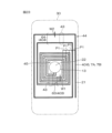
- FIG. 1 is a perspective view showing the state of use of an electrical stimulator.
- 2 is a schematic front view of the conductor of FIG. 1.
- FIG. 3 is a schematic rear view (first embodiment) of the conductor of FIG. 1.
- FIG. 4 is a schematic rear view (second form) of the conductor of FIG. 1.
- FIG. 5 is a schematic rear view (third embodiment) of the conductor of FIG. 1.
- FIG. 6 is a diagram showing a first modification of the electrode wiring pattern of FIG.
- FIG. 9 is a schematic front view of the device main body of FIG. 1.
- FIG. 10 is a schematic rear view of the device main body of FIG.
- FIG. 11 is a schematic plan view of the device main body of FIG. 1.
- FIG. 12 is a diagram showing a modification of the device main body of FIG.
- FIG. 13 is a diagram for explaining slits (first pattern) formed in the conductor.
- FIG. 14 is a diagram for explaining slits (second pattern) formed in the conductor.
- FIG. 15 is a diagram showing a modification of the arrangement direction of the slits in FIG.
- FIG. 16 is a diagram for explaining slits (third pattern) formed in the conductor.
- 17A and 17B are diagrams showing the state in which the slit is opened.
- FIG. 18 is a diagram showing thickness distribution (first pattern) in the conductive rubber layer.
- FIG. 19 is a cross-sectional view along line XIX-XIX in FIG. 18.
- FIG. 20 is a diagram showing thickness distribution (second pattern) in the conductive rubber layer.
- 21 is a cross-sectional view taken along line XXI-XXI of FIG. 20.
- FIG. 22 is a diagram showing a dense state of electrode wiring.
- FIG. 23 is a diagram showing a dense state of electrode wiring.
- FIG. 24 is a diagram for explaining the easy-to-separate processed portion of the sheet base material.
- FIG. 25 is a schematic perspective view of the mounting supporter.
- FIG. 26 is a schematic perspective view of the mounting supporter.
- 27A and 27B are diagrams showing states before and after deformation of the conductor pad portion.
- FIG. 28 is a diagram showing a state in which the conductor is attached using the attachment supporter.
- FIG. 29 is a diagram showing a state in which the conductor is attached using the attachment supporter.
- FIG. 30 is a diagram showing a state in which the conductor is attached using the attachment supporter.
- FIG. 1 is a perspective view showing the state of use of the electrical stimulator 1.
- FIG. 1 is a perspective view showing the state of use of the electrical stimulator 1.
- the electrical stimulation device 1 is, for example, a device (electrical stimulation treatment device).
- the electrical stimulator 1 will be mainly described as a device for treating dysuria, but the electrical stimulator 1 can treat not only dysuria but also urge fecal incontinence by electrical stimulation from the back side of the sacrum. , also contributes to the improvement of fecal incontinence, such as leaky fecal incontinence.
- the electrical stimulator 1 includes a conductor 2 for electrical stimulation, a device body 3, and a wiring cord 4.
- the electrode 2 includes a sheet base material 5, an indifferent electrode 6 and a pair of stimulation electrodes 7A, 7B. Since the conductor 2 is a sheet to which a plurality of electrodes are attached, it may be called an electrode pad, for example.
- Conductive sheets 8, 9A and 9B are attached to the indifferent electrode 6 and the pair of stimulating electrodes 7A and 7B, respectively.
- the conductive sheets 8, 9A, 9B may be prepared separately from the conductor 2 and attached at the time of use, or may be attached in advance to the electrodes 6, 7A, 7B as a standard form of the conductor 2 when shipped from the factory. may have been In the latter case, a protective film may be provided on the conductive sheets 8, 9A, 9B to prevent the conductive sheets 8, 9A, 9B from accidentally contacting and sticking to something.
- the conductive sheets 8, 9A, 9B are made of conductive adhesive gel, for example, in order to pass the current output from the pair of stimulating electrodes 7A, 7B to the human body 10.
- the conductive sheets 8, 9A, 9B are composed of pads having a thickness of about 0.8 mm.
- the conductive sheets 8, 9A, and 9B are translucent and have adhesiveness on both sides.
- the conductive sheets 8, 9A, and 9B are in the form of a translucent gel having adhesiveness, and may be called, for example, a conductive adhesive pad, a conductive gel pad, or the like.
- the electrode 2 is fixed to the skin of the human body 10 by attaching one surface of the conductive sheets 8, 9A, and 9B to the skin of the human body 10 (living body).
- an electrically conductive sheet 8 is attached to the indifferent electrode 6
- an electrically conductive sheet 9A is attached to one stimulation electrode 7A
- an electrically conductive sheet 9B is attached to the other stimulation electrode 7B.
- the device body 3 is electrically connected to the conductor 2 by a wiring cord 4 .
- the device body 3 incorporates a control circuit including, for example, a CPU, a memory such as a ROM and a RAM, and a timer.
- the patient can output an electric signal (voltage) for outputting a current of a predetermined frequency to the conductor 2 by operating various operation buttons 26 and the monitor 24 provided on the device main body 3. .
- electrical stimulation is applied to the human body 10 from the pair of stimulating electrodes 7A and 7B of the conductor 2.
- FIG. 2 is a schematic front view of the conductor 2 of FIG. 1.
- FIG. FIG. 3 is a schematic rear view (first form) of the conductor 2 of FIG.
- FIG. 4 is a schematic rear view (second form) of the conductor 2 of FIG.
- FIG. 5 is a schematic rear view (third form) of the conductor 2 of FIG.
- 6 and 7 are diagrams respectively showing a first modification and a second modification of the pattern of the electrode wiring 21 of FIG.
- the electrode 2 includes a sheet base material 5, an indifferent electrode 6 and a pair of stimulation electrodes 7A, 7B.
- the sheet base material 5 is made of a flexible material that can be bent according to the bending (movable) of the human body 10 .
- the sheet base material 5 is a planar sheet member having insulating properties and having a first surface 11 pressed against the surface of the human body 10 and a second surface 12 opposite to the first surface 11.
- the shape of the sheet base material 5 is, in this embodiment, a rectangular shape with rounded corners (FIGS. 3 and 5 to 7) or a substantially triangular shape (FIG. 4), but is not particularly limited. It can be changed as appropriate according to the shape of the target site for electrical stimulation in 10 .
- the shape of the sheet base material 5 may be square, circular, or the like.
- the sheet base material 5 examples include insulating materials such as resin films, nonwoven fabrics, and paper. These may be used alone or in combination of two or more.
- the sheet substrate 5 is made of paper.
- paper examples include natural paper made from natural materials such as wood pulp and cotton pulp, synthetic paper made from synthetic resin materials such as synthetic resin pulp, and mixed materials of natural and synthetic resin materials. Any of the mixed papers used as raw materials may be used.
- the sheet base material 5 is made of paper, it is possible to provide the conductor 2 as a disposable item that is discarded after being used for a certain period of time.
- conductive sheets 8, 9A, and 9B conductive gel
- the adhesion of dirt, dust, etc. to the adhesive surface may increase the electrical resistance value of the conductive gel, making it difficult to output sufficient electrical stimulation to the human body. Therefore, it is preferable to replace the conductive gel periodically.
- the conductor 2 is a disposable item, the conductor 2 can be discarded together with the conductive gel without removing only the conductive gel when replacing the conductive gel. Therefore, when using the electrostimulator 1 on a daily basis, replacement work of the conductive gel is unnecessary. In particular, replacement work including alignment of the conductive gel is difficult for the elderly, so the burden during use is reduced.
- the thickness of the sheet base material 5 is not particularly limited as long as it has a strength that can withstand use as the electrode 2 for electrical stimulation, but may be, for example, 0.05 mm to 5 mm. .
- the second surface 12 of the sheet base material 5 is provided with a first terminal 19 and second terminals 20A and 20B as an example of a connecting portion.
- the first terminal 19 and the second terminals 20A, 20B are snap terminals 13 in this embodiment.
- the structure of the first terminal 19 will be specifically described with reference to FIG. Since the specific structure of the second terminals 20A and 20B is the same as that of the first terminal 19, detailed description thereof will be omitted.
- the snap terminals 13 are fixed so as to sandwich the sheet base material 5 and are exposed on both the first surface 11 and the second surface 12 of the sheet base material 5 .
- the snap terminal 13 is a male terminal in this embodiment and has a stud portion 14 projecting from the second surface 12 of the sheet substrate 5 .
- This stud portion 14 is used as a terminal portion for external connection, and is electrically connected to the electrical stimulator 1 via the wiring cord 4 .
- a snap terminal 16 (female terminal) covered with a cover 15 made of resin, for example, is provided at the tip of the wiring cord 4 .
- a recess 17 is formed in the snap terminal 16 .
- the snap terminal 16 is snap-coupled to the snap terminal 13 by fitting the stud portion 14 into the recess 17 .
- the number of snap terminals 13 is not particularly limited. In FIG. 2, as an example, two snap terminals 13 are provided on the side of the indifferent electrode 6, and one snap terminal 13 is provided on each side of the pair of stimulation electrodes 7A and 7B.
- the connection between the first terminal 19 and the second terminals 20A and 20B and the wiring cord 4 is not limited to the snap connection described above, and may be, for example, an insertion connection.
- an insertion type connector male type
- insertion openings thereof may be provided in the first terminal 19 and the second terminals 20A and 20B.
- the first terminal 19 and the second terminals 20A, 20B are formed of a conductive metal that attracts magnets, and the contact force between the first terminal 19 and the second terminals 20A, 20B is applied to the tip of the wiring cord 4 by magnetic force.
- a connector may be provided to maintain the
- An indifferent electrode 6 and a pair of stimulation electrodes 7A and 7B are formed on the first surface 11 of the sheet base material 5, respectively.
- first to third configurations of the indifferent electrode 6 and the pair of stimulating electrodes 7A, 7B will be described, respectively.
- the configurations of the indifferent electrode 6 and the pair of stimulation electrodes 7A and 7B are not limited to the structures shown in FIGS.
- the first form shown in FIG. 3 may be selectively applied only to the indifferent electrode 6, and the third form shown in FIGS. 5 to 7 may be applied to the pair of stimulation electrodes 7A and 7B.
- the indifferent electrode 6 and the pair of stimulation electrodes 7A and 7B may be formed of a conductive rubber layer 18 as an example of a conductive layer.
- the conductive rubber layer 18 is formed of a silicone rubber layer containing conductive carbon such as carbon black in this embodiment.
- the material of the conductive rubber layer 18 is not limited to silicone rubber containing carbon black, as long as it is a conductive rubber.
- the conductor (conductive filler) mixed in the silicone rubber may be carbon black, silver powder, gold-plated silica or graphite, conductive zinc oxide, or the like.
- ion conductive silicone rubber may be used as the material for the conductive rubber layer 18 .
- the conductive rubber layer 18 is formed in a planar shape covering a certain area of the first surface 11 of the sheet base material 5 .
- the “planar shape covering a certain area” is, for example, a shape that entirely covers a portion having a certain width on the first surface 11 of the sheet base material 5 .
- it can be defined as a square, a rectangle, a triangle, a circle, or the like, and may be a shape that is distinguished from line-shaped wiring.
- the conductive rubber layer 18 is formed in a rectangular shape to contact and cover the conduction point 22 of the snap terminal 13 exposed from the first surface 11 .
- the conductive rubber layer 18 is electrically connected to the snap terminals 13 via the conduction points 22 .
- the shape of the conductive rubber layer 18 is rectangular in this embodiment, it is not particularly limited and can be changed as appropriate according to the shape of the target region of the human body 10 for electrical stimulation.
- the shape of the conductive rubber layer 18 may be square, circular, triangular, or the like.
- the thickness of the conductive rubber layer 18 is not particularly limited, but may be, for example, 10 ⁇ m to 5000 ⁇ m.
- the conductive rubber layer 18 can be formed, for example, by coating a dispersion liquid in which conductive carbon is dispersed on the first surface 11 of the sheet base material 5 in a predetermined shape and solidifying the liquid.
- the electrode wiring 21 may be formed by a conductive wire having a predetermined width in this embodiment.
- Examples of the material of the electrode wiring 21 include silver, copper, etc.
- silver silver chloride (AgAgCl) wiring is used.
- the electrode wiring 21 is connected to the snap terminal 13 in a certain area of the first surface 11 of the sheet base material 5 at a connection point 22 (for example, a portion of the snap terminal 13 exposed from the first surface 11 of the sheet base material 5). It is stretched all around.
- the "certain region of the first surface 11" is a region to be brought into contact with the target site of electrical stimulation on the human body 10, for example, a region having a shape substantially matching the conductive sheets 8, 9A, 9B. good too. Therefore, the area where the electrode wiring 21 is formed may be defined as the gel placement area 30 .
- the gel placement region 30 is indicated by a phantom line consisting of two-dot chain lines.
- the electrode wiring 21 may be formed in a spiral pattern with one line surrounding the conduction point 22 starting from one point of the conduction point 22 .
- the electrode wiring 21 is formed by a plurality of mutually independent lines extending from a plurality of locations of the conduction points 22, and each line reciprocates in a serpentine pattern to form a gel. It may be spread all over the arrangement area 30 .
- the electrode wiring 21 may be formed in a radial pattern extending from a plurality of conductive points 22 as shown in FIG. By forming the electrode wirings 21 in this way, the electrode wirings 21 have a pattern in which they are arranged at intervals. Also, the electrode wiring 21 is electrically connected to the snap terminal 13 via the conduction point 22 .
- the width of the electrode wiring 21 is not particularly limited, it may be, for example, 0.5 mm to 10 mm.
- the thickness of the electrode wiring 21 is not particularly limited, but may be, for example, 10 ⁇ m to 5000 ⁇ m.
- the interval (pitch) of the electrode wiring 21 is not particularly limited, but may be, for example, 0.5 mm to 10 mm.
- the electrode wiring 21 is formed by, for example, printing a predetermined wiring pattern on the first surface 11 of the sheet base material 5 with a conductive ink containing a conductive substance (eg, silver-silver chloride ink, copper ink, etc.) and solidifying the ink. can be formed by [Configuration of the device body]
- FIG. 9 is a schematic front view of the device main body 3 of FIG. 1.
- FIG. 10 is a schematic rear view of the device main body 3 of FIG. 1.
- FIG. FIG. 11 is a schematic plan view of the device main body 3 of FIG. 1.
- FIG. 9 is a schematic front
- the device body 3 is a portable electrical stimulation therapy device.
- the device body 3 includes a housing 23 , a monitor 24 provided on the front surface of the housing 23 , and a start/stop button 25 and a plurality of operation buttons 26 provided below the monitor 24 .
- the housing 23 is formed in a substantially elliptical shape in this embodiment, and may be made of a plastic case, for example.
- a first insertion port 27 and a second insertion port 28 are provided on the upper surface of the housing 23 .
- the first receptacle 27 is, for example, an output port to which the wiring cord 4 is connected.
- the second receptacle 28 is, for example, a port for charging, and a cord of an AC adapter (not shown) is connected. That is, the device main body 3 can be turned on by power supplied from an outlet via a charged battery or an AC adapter.
- the monitor 24 may be formed in a long rectangular shape along the longitudinal direction of the housing 23 and arranged near one end in the longitudinal direction of the housing 23 . Also, the monitor 24 may be, for example, a monochrome or color liquid crystal monitor.
- the monitor 24 can display, for example, the pulse waveform and frequency of the electrical stimulation signal from the pair of stimulation electrodes 7A and 7B, the patient's electrocardiographic waveform and heart rate, messages to be notified to the patient, and the like. can. Thereby, the person to be treated can easily know the operating state of the electrical stimulation device 1 .
- the monitor 24 may be, for example, a touch panel on which a predetermined operation screen is displayed and the screen can be operated.
- the start/stop button 25 and the plurality of operation buttons 26 may be arranged on the other end side in the longitudinal direction of the housing 23 with respect to the monitor 24 .
- the operation button 26 may have various functions depending on the model of the electrical stimulation device 1 .
- a treatment menu including pulse wave widths (pulse widths) and frequencies of stimulation signals suitable for each of a plurality of subjects is stored in the device main body 3, and the treatment menus are stored in the device main body 3. It may be a button or the like that is operated when reading.
- the device main body 3 has a built-in reader 29 .
- the reader 29 may be built into the housing 23 on the other longitudinal end side of the housing 23 with respect to the monitor 24, or as shown in FIG. may be built into the
- the reader 29 may include, for example, a reader for reading RF tags used for RFID (Radio Frequency IDentifier).
- the device main body 3 may have a modified configuration shown in FIG. Referring to FIG. 12, device main body 3 is an installation type electrical stimulation therapy device.
- the device main body 3 is used in a state where it is always installed in a facility such as a hospital.
- the device main body 3 includes a housing 58, a monitor 59, a power button 60, an operation button 61, and a port 62 as a physical configuration.
- the housing 58 is formed in a substantially rectangular shape in this embodiment, and may be made of a plastic case, for example. Although not shown, the rear surface of the housing 58 may be provided with an insertion port for connecting an AC adapter or the like.
- the monitor 59 is provided on the front surface of the housing 58 .
- the monitor 59 may be formed in a long rectangular shape along the longitudinal direction of the housing 58 .
- Monitor 59 may be, for example, a monochrome or color liquid crystal monitor.
- the monitor 59 may be, for example, a touch panel on which a predetermined operation screen is displayed and the screen can be operated.
- the power button 60 and the operation button 61 are provided below the monitor 59, for example.
- the operation button 61 may have various functions depending on the model of the device body 3 .
- a treatment menu including pulse wave widths (pulse widths) and frequencies of stimulation signals suitable for each of a plurality of subjects is stored in the device main body 3 and read out. It may be a button or the like that is operated at the time.
- a plurality of ports 62 are provided on the front surface of the housing 58 .
- One conductor 2 is connected to each port 62 through the wiring cord 4 .
- the conductors 2 By connecting the conductors 2 to the ports 62 one by one, multiple patients can receive electrical stimulation therapy at the same time.
- the indifferent electrode and the stimulating electrode are formed in a flat sheet shape as a whole. Therefore, when the sheet is attached to the surface of a living body, a part of the electrode attachment surface may not be properly attached, and the sheet may be wrinkled. As a result, a space such as air bubbles is formed between the sheet and the surface of the living body, and electrical stimulation may not be efficiently transmitted to the surface of the living body. As a result, sufficient electrical stimulation cannot be output to the living body, and sufficient effects of electrical stimulation may not be obtained.
- slits 31, 32, and 33 are formed for three-dimensionally deforming the sheet base material 5. Variations in the pattern of the slits 31 to 33 will be described below with reference to FIGS. 13 to 16. FIG.
- FIG. 13 is a diagram for explaining the slits 31 (first pattern) formed in the conductor 2.
- FIG. FIG. 13 is a diagram corresponding to FIG. 3, in which the indifferent electrode 6 and the pair of stimulating electrodes 7A and 7B are formed of a conductive rubber layer 18.
- the width direction (horizontal direction) of the conductor 2 is defined as the first direction X
- the length direction (vertical direction) of the conductor 2 is defined as the second direction Y for convenience.
- a second direction Y is a direction orthogonal to the first direction X.
- the slit 31 is formed on almost the entire surface of the sheet base material 5.
- a plurality of slits 31 are formed in the sheet base material 5 .
- the slits 31 include linear first slits 311 extending in the first direction X and linear second slits 312 extending in the second direction Y.
- the first slits 311 and the second slits 312 are regularly arranged on the sheet base material 5 . More specifically, along the first direction X and the second direction Y, the first slits 311 and the second slits 312 are alternately arranged.
- the plurality of first slits 311 are arranged in a zigzag pattern so as not to be adjacent to each other in the first direction X and the second direction Y.
- the plurality of second slits 312 are arranged in a zigzag pattern so as not to be adjacent to each other in the first direction X and the second direction Y. As shown in FIG.
- Each first slit 311 and each second slit 312 have first ends 311A, 312A and opposite second ends 311B, 312B, respectively. Some of the first slits 311 and the second slits 312 may be formed so as to penetrate the sheet substrate 5 in regions where the conductive rubber layer 18 is not formed on the sheet substrate 5 . In addition, some other first slits 311 and second slits 312 are formed so as to overlap the conductive rubber layer 18 in the region where the conductive rubber layer 18 is formed in the sheet base material 5. good. Therefore, some first slits 311 and second slits 312 may continuously penetrate the conductive rubber layer 18 and the sheet base material 5 .
- At least one end 311A, 312A, 311B, 312B of each of the first slits 311 and each of the second slits 312 overlapping the conductive rubber layer 18 is arranged inside the outer peripheral edge 181 of the conductive rubber layer 18. .
- the conductive rubber layer 18 is not divided by the slits 31 . Therefore, electrical connection between the snap terminal 13 and the conductive rubber layer 18 can be secured over the entire conductive rubber layer 18 .
- FIG. 14 is a diagram for explaining the slits 32 (second pattern) formed in the conductor 2.
- FIG. FIG. 15 is a diagram showing a modification of the arrangement direction of the slits 32 in FIG. 14 and 15 are diagrams corresponding to FIG. 3, in which the indifferent electrode 6 and the pair of stimulation electrodes 7A and 7B are formed of a conductive rubber layer 18.
- FIG. 14 for convenience, the direction inclined by 45° with respect to the width direction (horizontal direction) of the conductor 2 is defined as the first direction X, and the direction orthogonal to the first direction X is defined as the second direction Y.
- the slit 32 is formed on almost the entire surface of the sheet base material 5.
- a plurality of slits 32 are formed in the sheet base material 5 .
- the slits 32 include linear first slits 321 extending in the first direction X and linear second slits 322 extending in the second direction Y.
- the first slits 321 and the second slits 322 are regularly arranged on the sheet base material 5 . More specifically, each of the plurality of slits 32 is formed as a cross slit by the first slit 321 and the second slit 322 crossing each other.
- a plurality of cross slits 32 are arranged in a matrix on the sheet base material 5 .
- the orientation of the plurality of cross slits 32 may be an X pattern as shown in FIG. 14 or a cross pattern as shown in FIG.
- Each first slit 321 and each second slit 322 have first ends 321A, 322A and opposite second ends 321B, 322B, respectively. Some of the first slits 321 and the second slits 322 may be formed to penetrate the sheet substrate 5 in regions where the conductive rubber layer 18 is not formed on the sheet substrate 5 . In addition, some other first slits 321 and second slits 322 are formed so as to overlap the conductive rubber layer 18 in the region where the conductive rubber layer 18 is formed in the sheet base material 5. good. Therefore, some first slits 321 and second slits 322 may continuously penetrate the conductive rubber layer 18 and the sheet base material 5 .
- At least one end 321A, 322A, 321B, 322B of each of the first slits 321 and each of the second slits 322 overlapping the conductive rubber layer 18 is arranged inside the outer peripheral edge 181 of the conductive rubber layer 18. .
- the conductive rubber layer 18 is not divided by the slits 32 . Therefore, electrical connection between the snap terminal 13 and the conductive rubber layer 18 can be secured over the entire conductive rubber layer 18 .
- FIG. 16 is a diagram for explaining the slits 33 (third pattern) formed in the conductor 2.
- FIG. 16 is a diagram corresponding to FIG. 5, in which the indifferent electrode 6 and the pair of stimulating electrodes 7A and 7B are formed by electrode wiring 21.
- the width direction (horizontal direction) of the conductor 2 is defined as the first direction X
- the length direction (vertical direction) of the conductor 2 is defined as the second direction Y for convenience.
- a second direction Y is a direction orthogonal to the first direction X.
- the number of turns of the electrode wiring 21 is reduced and the interval between the electrode wirings 21 is widened.
- a plurality of slits 33 are formed in the region 34 between the adjacent electrode wirings 21.
- the region 34 may include a first region 341 extending in the first direction X and a second region 342 extending in the second direction Y. good.
- the multiple slits 33 include first slits 331 formed in the first region 341 and second slits 332 formed in the second region 342 .
- the first slit 331 and the second slit 332 are formed along the electrode wiring 21 so as not to cross the electrode wiring 21 respectively.
- the first slit 331 and the second slit 332 are formed parallel to the electrode wiring 21 .
- the electrode wiring 21 is not divided by the slits 33 . Therefore, electrical connection between the snap terminal 13 and the electrode wiring 21 can be ensured over the entire electrode wiring 21 .
- the common items of the slits 31 to 33 is added.
- a plurality of slits 31 to 32 are preferably formed from the viewpoint of deforming the conductor 2 more flexibly.
- the number of slits 31-33 is not particularly limited.
- the dimension (length) of each of the slits 31 to 33 may be, for example, 0.25 cm to 10 cm.
- the interval between the adjacent slits 31 to 33 is, for example, 0.25 cm to 1.5 cm from the viewpoint of preventing the sheet base material 5 from tearing from the slits 31 to 33 and connecting the slits 31 to 33 with each other. is preferred.
- FIG. 17A and 17B are diagrams showing the state in which the slit 31 is open. Next, the three-dimensional deformation of the conductor 2 by the slits 31 to 33 will be described with reference to the drawings relating to the slit 31.
- FIG. 17A and 17B are diagrams showing the state after the conductor 2 of FIG. 13 is deformed, but the number of slits 31 is reduced in order to clearly show the open state of the slits 31.
- the slits 31 to 33 are opened so that the sheet base material 5 can be three-dimensionally shaped according to the shape of the living body surface. can be transformed into Thereby, the electrode 2 can be well fitted to the surface of the living body.
- the sheet base material 5 can be flexibly deformed according to the shape of the living body surface.
- the slit 32 is a cross-shaped slit, it is possible to flexibly cope with deformation in all directions from the center of the cross-shaped slit 32 toward its periphery.
- the conductive sheets 8, 9A, 9B conductive gel
- the conductive sheets 8, 9A, 9B Air bubbles may occur between 9B and the conductive rubber layer 18 or electrode wiring 21 .
- air bubbles can be removed not only from the outer edges of the conductive sheets 8, 9A, and 9B, but also through the plurality of slits 31-33.
- the adhesion between the conductive sheets 8, 9A, and 9B and the conductive rubber layer 18 and the electrode wiring 21 can be improved (a large contact area can be secured). Electrical stimulation can be efficiently transmitted to the surface of the living body through the sheets 8, 9A, and 9B.
- regions are formed between the plurality of slits 31 to 33 to ensure electrical connection between the snap terminal 13 and the conductive rubber layer 18 (or between the snap terminal 13 and the electrode wiring 21).
- the entire conductive rubber layer 18 and electrode wiring 21 can be effectively used as a region for transmitting electrical stimulation to the surface of the living body.
- Electrode conductivity control For example, in the invention described in Patent Document 1, the indifferent electrode and the stimulating electrode are formed in a flat sheet shape as a whole. Therefore, the electrical resistance is uniform in the direction along the sheet surface, and voltage and current may be insufficient in areas where strong electrical stimulation is required, and excessive voltage and current may be supplied in areas where electrical stimulation is not so necessary. .
- the indifferent electrode 6 and the pair of stimulating electrodes 7A and 7B have different voltage and current magnitude distributions. Variations in voltage/current distribution of the indifferent electrode 6 and the pair of stimulation electrodes 7A and 7B will be described below with reference to FIGS. 18 to 23. FIG.
- FIG. 18 is a diagram showing the thickness distribution (first pattern) in the conductive rubber layer 18.
- FIG. 19 is a cross-sectional view along line XIX-XIX in FIG. 18.
- FIG. 18 and 19 selectively show the stimulation electrodes 7A shown in FIG. Since the thickness distribution of the conductive rubber layer 18 shown in FIG. 18 can be applied not only to the stimulating electrode 7A but also to the indifferent electrode 6 and the stimulating electrode 7B, in FIG. They are collectively defined as electrodes 35 .
- the conductive rubber layer 18 related to the electrode 35 in FIG. 18 includes a first portion 351 having a first thickness T1 and a second portion 352 having a second thickness T2 smaller than the first thickness T1.
- the relatively thick first portion 351 has a wider current path than the relatively thin second portion 352, resulting in a smaller resistance.
- the resistance value (first resistance value) of the first portion 351 may be 5 ⁇ to 10 ⁇
- the resistance value (second resistance value) of the second portion 352 may be 10 ⁇ to 50 ⁇ .
- the first thickness T1 may be, for example, 50 ⁇ m to 500 ⁇ m
- the second thickness T2 may be, for example, 10 ⁇ m to 50 ⁇ m.
- it may be continuously changed in the range of 5 ⁇ to 50 ⁇ and 10 ⁇ m to 500 ⁇ m between the first portion 351 and the second portion 352 .
- the conductive rubber layer 18 includes the first portion 351 and the second portion 352 having different resistance values, the voltage/current distribution is flexibly adjusted according to the biological site to which the conductor 2 is attached. be able to. For example, there is no need to separately form or embed a predetermined pattern of conductive material in the conductive rubber layer 18 in order to adjust the voltage/current distribution, so the structure of the conductor 2 can be simplified.
- the first portion 351 and the second portion 352 divide the coating amount of the coating liquid (in this embodiment, the dispersion liquid in which the conductive carbon is dispersed) when forming the conductive rubber layer 18 for each location. can be easily formed by
- the second portion 352 of the conductive rubber layer 18 is formed on the outer peripheral edge portion 36 of the conductive rubber layer 18, and the first portion 351 of the conductive rubber layer 18 is formed inside the outer peripheral edge portion 36. It is formed in the central region 37 .
- the outer peripheral edge portion 36 may be, for example, a portion extending inward from the outer peripheral edge 181 of the conductive rubber layer 18 (outline line of the conductive rubber layer 18) to 0.5 cm.
- the central region 37 may be the region surrounded by the outer peripheral edge 36 . Since the boundary between the first portion 351 and the second portion 352 is not straight like a line drawn with a ruler, in FIG. The area where the two parts 352 are formed is indicated by the white area around the hatching.
- the base material of the conductor 2 is the sheet base material 5 as in this embodiment, for example, when the conductor 2 is attached to the surface of the living body, a part of the outer peripheral edge portion 36 of the conductive rubber layer 18 is the surface of the living body. floating from the If electrical stimulation is applied to the living body surface from the electrode 2 in this state, a tingling pain may be felt in the vicinity of the outer peripheral edge 36 of the conductive rubber layer 18 . Therefore, according to the configuration of FIG. By increasing the resistance value of 36, it is possible to reduce the magnitude of the voltage/current at that portion. As a result, even if part of the outer peripheral edge portion 36 of the conductive rubber layer 18 is floating, it is possible to reduce discomfort such as prickling pain.
- FIG. 20 is a diagram showing the thickness distribution (second pattern) in the conductive rubber layer 18.
- FIG. 21 is a cross-sectional view taken along line XXI-XXI of FIG. 20.
- FIG. 20 and 21, as in FIG. 18, the indifferent electrode 6 and stimulating electrodes 7A and 7B are collectively defined as electrodes 35 for convenience. 18, 20, and 21 are denoted by the same reference numerals, and description thereof will be omitted.
- the second portion 352 of the conductive rubber layer 18 is formed in the terminal vicinity region 38 around the connection point 22 between the conductive rubber layer 18 and the snap terminal 13, and the first portion 352 of the conductive rubber layer 18 is formed. 351 is further around the second portion 352 and is formed in the terminal spacing region 39 away from the snap terminal 13 .
- the near-terminal region 38 may be, for example, a peripheral portion up to 5 cm from the snap terminal 13 .
- the terminal vicinity region 38 may be an outer peripheral portion around the snap terminal 13 and may be a region up to half of the width of the portion with the smallest width to the outer peripheral edge 181 of the conductive rubber layer 18 .
- the terminal separation region 39 may be a region from the terminal vicinity region 38 to the outer peripheral edge 181 of the conductive rubber layer 18 .
- the second portion 352 is also formed on the outer peripheral edge portion 36 of the conductive rubber layer 18, similarly to FIG.
- the entire conductive rubber layer 18 is Uniformity of voltage/current distribution can be achieved.
- FIG. 22 is a diagram showing a dense state of the electrode wirings 21.
- FIG. FIG. 22 selectively shows the stimulation electrodes 7A shown in FIG. 22 can be applied not only to the stimulating electrode 7A but also to the indifferent electrode 6 and the stimulating electrode 7B. Therefore, in FIG. Defined as electrode 40 .
- a dense pattern region 41 in which the electrode wirings 21 are arranged at a first interval W1 and a sparse pattern region 42 in which the electrode wirings 21 are arranged at a second interval W2 wider than the first interval W1. is formed.
- the dense pattern area 41 is an area where the electrode wirings 21 are denser than the sparse pattern area 42 .
- the number of electrode wirings 21 crossing the unit areas 43 having the same unit length is greater in the dense pattern area 41 than in the sparse pattern area 42 .
- the number of electrode wirings 21 crossing the unit area 43 of the sparse pattern area 42 is two, whereas the number of electrode wirings 21 crossing the unit area 43 of the dense pattern area 41 is six.
- the electrode wiring 21 includes a first portion 401 having a relatively low first resistance value and a second portion 402 having a second resistance value higher than the first resistance value.
- the resistance value (first resistance value) of the first portion 401 may be 5 ⁇ to 10 ⁇
- the resistance value (second resistance value) of the second portion 402 may be 10 ⁇ to 50 ⁇ .
- the first spacing W1 between the electrode wirings 21 in the dense pattern area 41 may be, for example, 0.5 mm to 5 mm
- the second spacing W2 between the electrode wirings 21 in the sparse pattern area 42 may be, for example, 5 mm to 10 mm.
- the distance between the first interval W1 of the dense pattern region 41 and the second interval W2 of the sparse pattern region 42 of the electrode wiring 21 may be changed continuously within a range of 0.5 mm to 10 mm.
- the second portion 402 of the electrode wiring 21 is formed in the outer peripheral edge portion 44 of the gel placement region 30, and the first portion 401 of the electrode wiring 21 is formed in the central region 45 inside the outer peripheral edge portion 44.
- the outer peripheral edge portion 44 may be, for example, a portion up to 0.5 cm inward from the outer peripheral edge 301 of the gel placement region 30 (the line where the outer peripheral edge of the conductive gel to be placed is supposed to be positioned).
- the central region 45 may be a region surrounded by the outer peripheral edge 44 .
- the second portion 402 having a relatively high second resistance value is arranged at the outer peripheral edge portion 44 of the gel placement region 30 , thereby increasing the resistance value of the outer peripheral edge portion 44 of the gel placement region 30 .
- the first portion 401 and the second portion 402 can be easily distinguished and formed by simply setting the printing pattern of the conductive ink when forming the electrode wiring 21 .
- FIG. 23 is a diagram showing another form of the dense state of the electrode wirings 21.
- FIG. FIG. 23 selectively shows the stimulation electrodes 7A shown in FIG. Since the dense state of the electrode wiring 21 shown in FIG. 23 can be applied not only to the stimulating electrode 7A but also to the indifferent electrode 6 and the stimulating electrode 7B, in FIG. Defined as electrode 40 .
- the electrode wiring 21 is spirally formed at a constant interval (pitch) P1.
- the electrode wiring 21 includes a dense pattern region 63 formed by wiring having a first width W1 and a sparse pattern region 64 formed by wiring having a second width W2 narrower than the first width W1. . Due to this width difference, the dense pattern region 63 is a region in which the electrode wirings 21 are denser than in the sparse pattern region 64 . For example, the area of the electrode wiring 21 crossing the unit areas 43 having the same unit length is larger in the dense pattern area 63 than in the sparse pattern area 64 .
- the electrode wiring 21 includes a first portion 403 having a relatively low first resistance value and a second portion 404 having a second resistance value higher than the first resistance value.
- the resistance value (first resistance value) of the first portion 403 may be 5 ⁇ to 10 ⁇
- the resistance value (second resistance value) of the second portion 404 may be 10 ⁇ to 50 ⁇ .
- the second portion 404 of the electrode wiring 21 is formed in the outer peripheral edge portion 44 of the gel placement region 30, and the first portion 403 of the electrode wiring 21 is formed in the central region 45 inside the outer peripheral edge portion 44.
- the outer peripheral edge portion 44 may be, for example, a portion up to 0.5 cm inward from the outer peripheral edge 301 of the gel placement region 30 (the line where the outer peripheral edge of the conductive gel to be placed is supposed to be positioned).
- the central region 45 may be a region surrounded by the outer peripheral edge 44 .
- the second portion 404 having a relatively high second resistance value is arranged on the outer peripheral edge portion 44 of the gel placement region 30 , thereby increasing the resistance value of the outer peripheral edge portion 44 of the gel placement region 30 .
- the first portion 403 and the second portion 404 can be easily distinguished and formed simply by setting the printing pattern of the conductive ink when forming the electrode wiring 21 .
- a sparse pattern region 64 is formed in the terminal vicinity region 38 and a dense pattern region 63 is formed in the terminal separation region 39 as shown in FIG. Uniformity of current distribution can be achieved.
- the conductor 2 is a disposable item having a sheet base material 5 made of paper
- the conductor 2 is discarded as it is after using the conductor for a certain period of time.
- the combustible sheet base material 5 formed of paper and the flame-retardant snap terminal 13 formed of metal are mixed in the conductor 2, the snap terminal 13 is removed and separated. There is a need.
- FIG. 24 is a diagram for explaining the easily separable portion 46 of the sheet base material 5.
- the easy-to-separate processed portion 46 is a portion formed by selectively processing a part of the sheet base material 5 and provides easy separation of the snap terminal 13 .
- the easily separable portion 46 is formed so as to surround the snap terminal 13 .
- the easily separable processed portion 46 surrounds substantially the entire circumference of the snap terminal 13 .
- the structure of the easily separable portion 46 is not particularly limited, but in this embodiment, it is a perforation line 47 formed so as to surround the snap terminal 13 .
- a knob 48 that can be raised from the sheet base material 5 may be formed on a part of the perforation line 47 in the circumferential direction. For example, by holding the knob 48 and pulling it forward, a portion of the sheet base material 5 surrounded by the perforation line 47 (between the terminal region 49 and its periphery) is torn with the perforation line 47 as a boundary. . Thereby, the snap terminal 13 is separated from the sheet substrate 5 together with the terminal area 49 . As a result, the sheet base material 5 made of paper and the snap terminal 13 made of metal can be easily separated, and can be separately discarded.
- the easy-to-separate processed portion 46 is not limited to the perforation line 47.
- a portion of the sheet base material 5 may be selectively thinned in a line shape (in FIG. 24, an annular ring surrounding the snap terminal 13). It may also be a formed tearable portion.
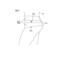
- [Configuration of mounting supporter] 25 is a schematic perspective view of the mounting supporter 50.
- FIG. FIG. 26 is a schematic perspective view of the mounting supporter 50.
- FIG. 27A and 27B are diagrams showing states before and after deformation of the conductor pad portion 51.
- FIG. 28 to 30 are diagrams showing a state in which the conductor is attached using the attachment supporter 50.
- FIG. 28 is a view of the human body 10 viewed from the front side
- FIG. 29 is a view of the human body 10 viewed from the back side
- FIG. 30 is a view of the human body 10 viewed from the left lateral side.
- the mounting supporter 50 is a device that assists the mounting of the electrode 2.
- the mounting supporter 50 includes a conductor pad portion 51 as an example of a conductor holding portion that holds the conductor 2 and a belt 52 connected to the conductor pad portion 51 .
- the mounting supporter 50 may integrally have a conductor pad portion 51 and a belt 52 formed of, for example, cloth.
- the conductor pad portion 51 and the belt 52 may be formed as separate parts and then connected to each other, for example, by sewing.
- the conductor pad portion 51 is provided in the center of the mounting supporter 50 .
- the conductor pad portion 51 is formed, for example, in a curved sheet shape recessed backward.
- the surface of the conductor pad portion 51 to which the second surface 12 of the sheet base material 5 is connected is a concave surface 53 .
- the planar shape of the conductor pad portion 51 is a substantially rectangular shape in accordance with the shape of the conductor 2, but may be other shapes such as a circular shape.
- a fixture 54 for fixing the conductor 2 to the conductor pad portion 51 is provided on the concave surface 53 .
- the fixture 54 is not particularly limited as long as it can fix the conductor 2, but it may be a snap button, for example.
- the belt 52 is stretchable in the left and right direction, and is connected to both the left and right sides of the conductor pad portion 51 .
- the belts 52 include a left belt 52L on the left side of the conductor pad portion 51 (right side in the drawing) and a right belt 52R on the right side of the conductor pad portion 51 (left side in the drawing).
- Each of the left belt 52L and the right belt 52R has two belts that are vertically spaced apart from each other.
- a fastener 55 for fixing the belts 52 to each other is provided at the tip of each belt 52 .
- the fastener 55 is not particularly limited as long as it can fix the belts 52 so that they do not separate from each other.
- FIG. 9B conductive gel
- the conductor 2 is fixed to the conductor pad portion 51 via the fixture 54 .
- the conductor 2 is held in a recessed shape along the concave surface 53 of the conductor pad portion 51 .
- a slit 31 see FIGS. 17A and 17B
- the slit 31 opens and the conductor 2 is three-dimensionally deformed, so that the conductor 2 is restrained from being stretched. It can be easily recessed along the concave surface 53 .
- the conductive sheets 8 , 9 A, and 9 B (conductive gel) can also be deformed into a recessed shape along the concave surface 53 . Therefore, as shown in FIG. 27A, until the conductor 2 is pressed against the surface of the human body 10, it is possible to prevent the conductive gel from inadvertently sticking to the surface of the body other than the target site for electrical stimulation, clothes, etc. can.
- the mounting supporter 50 is used to align the conductors 2 .
- the alignment is such that the conductor 2 rests on the back of the sacrum.
- a space 57 may be formed between the conductor 2 and the surface of the human body 10 .
- the belt 52 is pulled left and right and fixed with fasteners 55 as shown in FIG.
- FIG. 27B when the belt 52 is pulled left and right, the conductor pad portion 51 (curved sheet shape) is deformed so as to protrude forward in conjunction with the movement.
- the electrode 2 can be easily pressed against the surface of the human body 10. - ⁇ If the conductor 2 does not adhere to the surface of the human body 10 only by pulling the belt 52, the conductor pad portion 51 may be pushed from behind.
- the electrode 2 can be attached as shown in FIGS.
- two left belts 52L and two right belts 52R are provided with a vertical interval therebetween. Therefore, by fixing the mounting supporter 50 so as to sandwich the protrusion on the surface of the human body 10 such as the iliac crest 56 between the upper and lower belts 52, the positional deviation of the mounting supporter 50 can be suppressed.
- the base material is sheet-like
- the electrostimulation conductor when the electrostimulation conductor is attached to the surface of the living body, the base material follows the shape of the surface of the living body in the lateral direction (first surface and force is applied in the direction along the second surface).
- the slit is formed in the base material, the sheet-like base material can be three-dimensionally deformed according to the shape of the living body surface by opening the slit.
- the electrical stimulation conductor can be well fitted to the surface of the living body.
- air bubbles may be generated between the conductive gel and the conductive portion.
- air bubbles can be removed not only from the outer edge of the conductive gel but also through a plurality of slits.
- the adhesion between the conductive gel and the conductive portion can be improved (a large contact area can be secured), so that electrical stimulation can be efficiently transmitted from the conductive portion to the biological surface via the conductive gel.
- regions are formed between the plurality of slits to ensure electrical connection between the connecting portion and the conductive portion.
- the entire conductive portion can be effectively used as a region for transmitting electrical stimulation to the living body surface.
- Appendix 1-2 The electrical stimulation conductor according to Appendix 1-1, wherein the plurality of slits includes a first slit extending in a first direction and a second slit extending in a direction intersecting the first direction.
- the base material can be flexibly deformed according to the shape of the living body surface.
- Appendix 1-3 The electrical stimulation conductor according to Appendix 1-2, wherein the plurality of slits includes a cross slit formed by crossing the first slit and the second slit.
- Appendix 1-4 The electrical stimulation conductor according to Appendix 1-2 or Appendix 1-3, wherein the plurality of slits are formed by alternately arranging the first slits and the second slits.
- the first slits and the second slits having different opening directions can be evenly arranged without being biased for each region of the substrate surface.
- the substrate can be flexibly deformed according to the shape of the biological surface.
- the conductive part includes a conductive layer formed in a planar shape covering a certain area of the first surface of the base material,
- the plurality of slits have at least one end inside the outer peripheral edge of the conductive layer, and are formed to continuously penetrate the conductive layer and the base material, Appendix 1-1 to Appendix 1- 5.
- the electrode for electrical stimulation according to any one of 4.
- the base material and the conductive layer can be three-dimensionally deformed according to the shape of the living body surface by opening the slits. can. Moreover, since at least one end of the slit is located inside the outer peripheral edge of the conductive layer, the conductive layer is not divided by the slit. Thereby, the electrical connection between the connecting portion and the conductive layer can be secured over the entire conductive layer. Furthermore, since the conductive layer is formed in a planar shape, electrical stimulation can be efficiently transmitted to the living body surface from the entire region of the substrate where the conductive layer is formed.
- the conductive portion is an electrode wiring that is stretched around a point of conduction with the connection portion within a certain region of the first surface of the base material, and has patterns that are arranged at intervals.
- the electrical stimulation lead according to any one of Appendices 1-1 to 1-5, wherein the plurality of slits are formed along the electrode wiring in a region between the adjacent electrode wirings.
- the slit is formed in the region between the electrode wirings in the base material, a constant distance can be secured between the slits and the electrode wirings. Thereby, the insulation between the electrode wiring and the second surface side of the base material can be satisfactorily ensured. Also, since the slits are formed along the electrode wiring, the electrode wiring is not divided by the slits. Thereby, electrical connection between the connecting portion and the electrode wiring can be ensured over the entire electrode wiring.
- Appendix 1-7 The electrical stimulation conductor according to appendix 1-6, wherein the electrode wiring is spirally formed starting from the conduction point.
- the electrode for electrical stimulation as a disposable product, and since the discarded base material includes synthetic paper, it is possible to reduce the burden on the environment.
- a substrate formed of a sheet-like insulating material having a first surface to be pressed against the biological surface and a second surface on the opposite side; a conductive portion formed of a conductive material on the first surface of the base; a connecting portion formed on the second surface of the base material and conducting to the conductive portion;
- the conductive portion includes a first portion having a first resistance value, and a second portion having a second resistance value in a predetermined range selectively set higher than the first resistance value.
- the conductive portion includes the first portion and the second portion having different resistance values
- the voltage/current distribution can be flexibly adjusted according to the living body site to which the electrical stimulation conductor is attached. can be done. For example, it is not necessary to separately form or embed a predetermined pattern of conductive material in the conductive portion to adjust the voltage/current distribution, so the structure of the electrical stimulation conductor can be simplified.
- the conductive part includes a conductive layer formed in a planar shape covering a certain area of the first surface of the base material,
- the conductive layer includes the first portion having a first thickness and the second portion having a second thickness smaller than the first thickness,
- the electrical stimulation lead according to Appendix 1-9 is a conductive layer formed in a planar shape covering a certain area of the first surface of the base material,
- the conductive layer includes the first portion having a first thickness and the second portion having a second thickness smaller than the first thickness,
- the electrical stimulation lead according to Appendix 1-9 is a conductive layer formed in a planar shape covering a certain area of the first surface of the base material.
- the conductive portion is an electrode wiring that is stretched around a point of conduction with the connection portion within a certain region of the first surface of the base material, and has patterns that are arranged at intervals.
- the first surface of the base material includes a dense pattern region in which the electrode wirings are arranged at a first interval to form the first portion, and a dense pattern region in which the electrode wirings are arranged at a second interval wider than the first interval to form the first portion. and a sparsely patterned area forming two parts.
- the conductive portion is an electrode wiring that is stretched around a conductive point with the connection portion in a certain area of the first surface of the base material, and includes a pattern having electrode wiring with different widths,
- the first surface of the substrate includes a dense pattern area formed of the electrode wiring having a first width and a sparse pattern area formed of the electrode wiring having a second width narrower than the first width.
- the electrode for electrical stimulation according to appendix 1-9 comprising:
- the base material is sheet-like, for example, when the electrostimulation electrode is attached to the surface of the living body, part of the outer peripheral edge of the conductive part is in a state of floating from the surface of the living body. In this state, when electrical stimulation is applied from the electrode to the surface of the living body, a tingling pain may be felt in the vicinity of the outer peripheral edge of the conductive portion. Therefore, according to this configuration, by arranging the second portion having a relatively high second resistance value at the outer peripheral edge portion of the conductive portion, the resistance value of the outer peripheral edge portion of the conductive portion is increased to increase the resistance at the portion. voltage and current can be reduced. As a result, even if part of the outer peripheral edge of the conductive portion is floating, it is possible to reduce discomfort such as prickling pain.
- the second portion of the conductive portion is formed around a point of conduction with the connection portion in the conductive portion, and the first portion of the conductive portion is formed in a region further around the second portion.
- the electrode for electrical stimulation according to any one of Appendices 1-9 to 1-13.
- the voltage/current distribution is uniform. can be improved.
- Appendix 1-16 The electrical stimulation conductor according to any one of Appendixes 1-9 to 1-15, wherein the insulating material includes synthetic paper.
- the electrode for electrical stimulation as a disposable product, and since the discarded base material includes synthetic paper, it is possible to reduce the burden on the environment.
- the connecting portion includes a metal terminal fixed to the base material, Any one of Appendices 1-1 to 1-16, further comprising an easy-to-separate processed portion that is formed around the terminal in the base material and facilitates selective separation of a part of the base material together with the terminal.
- the metal terminals can be easily separated. Therefore, for example, when the electric stimulation conductor is a disposable product, the base material formed of the insulating material and the metal terminal can be easily separated and discarded.
- the cable of the electrical stimulation device that supplies electrical stimulation signals to the conductors can be easily connected to the connecting portion (snap terminal) by snap coupling, and can be easily removed.
- Appendix 1-20 The electrical stimulation conductor according to any one of Appendices 1-1 to 1-19, wherein the substrate comprises a paper substrate.
- the electrode for electrical stimulation as a disposable product, and since the discarded base material is made of paper, it is possible to reduce the burden on the environment.
- Appendix 1-21 a conductive gel formed to cover the conductive portion;
- the conductive gel is provided on the electrical stimulation conductor in advance, the work of attaching the conductive gel when using the conductor can be omitted. Moreover, since the conductive gel is covered with the protective film, it is possible to prevent the conductive gel from accidentally contacting and sticking to something.
- a conductor mounting supporter for assisting mounting of a sheet-like electrical stimulation conductor having a first surface to be pressed against a living body surface and a second surface on the opposite side thereof, Having a concave surface to which the second surface of the electrical stimulation conductor is connected along, and holding the electrical stimulation conductor in a recessed shape along the concave surface;
- a probe attachment supporter including a belt that is connected to the probe holding part and can be fixed to a living body.
- the electrical stimulation conductor can be held in a recessed shape along the concave surface.
- the conductive gel when the conductive gel is adhered to the conductive portion of the substrate and the conductor is used, the conductive gel can also be deformed into a recessed shape along the concave surface. Therefore, it is possible to prevent the conductive gel from inadvertently adhering to surfaces other than the electrical stimulation target site of the living body, clothes, etc., until the conductor is pressed against the surface of the living body.
- the electrode mounting supporter includes a supporter for mounting the electrode for electrical stimulation on the back of a person's waist
- the conductor holding portion includes a conductor pad portion formed in a curved sheet shape recessed backward
- the belt includes left and right belts connected to the left and right sides of the conductor pad portion,
- the conductor mounting supporter according to appendix 1-22 wherein when the belt is pulled left and right, the conductor pad section is deformed such that the curved sheet shape protrudes forward in conjunction with the movement of the belt.
- the electrode for electrical stimulation can be easily pressed against the surface of the living body.
- each of the left and right belts includes a plurality of belts that are vertically spaced apart from each other.
- the supporter can be restrained from being displaced by fixing the supporter so as to sandwich the protrusion of the living body surface such as the iliac crest between the upper and lower belts.
- Electrode 1 Electrical stimulation device 2: Electrode 3: Device main body 4: Wiring cord 5: Sheet base material 6: Indifferent electrode 7A: Stimulation electrode 7B: Stimulation electrode 8: Conductive sheet 9A: Conductive sheet 9B: Conductive sheet 10: Human body 11: First surface 12: Second surface 13: Snap terminal 14: Stud portion 15: Cover 16: Snap terminal 17: Recess 18: Conductive rubber layer 19: First terminal 20A: Second terminal 20B: Second terminal 2 terminals 21 : electrode wiring 22 : conduction point 23 : housing 24 : monitor 25 : stop button 26 : operation button 27 : first insertion port 28 : second insertion port 29 : reader 30 : gel placement area 31 : Slit 32 : Cross slit 33 : Slit 34 : Area 35 : Electrode 36 : Peripheral edge 37 : Central area 38 : Terminal vicinity area 39 : Terminal isolated area 40 : Electrode 41 : Dense pattern area 42 : Sparse pattern area 43 : Unit area 44 : Peripheral edge
Landscapes
- Health & Medical Sciences (AREA)
- Engineering & Computer Science (AREA)
- Biomedical Technology (AREA)
- Nuclear Medicine, Radiotherapy & Molecular Imaging (AREA)
- Radiology & Medical Imaging (AREA)
- Life Sciences & Earth Sciences (AREA)
- Animal Behavior & Ethology (AREA)
- General Health & Medical Sciences (AREA)
- Public Health (AREA)
- Veterinary Medicine (AREA)
- Electrotherapy Devices (AREA)
Abstract
電気刺激用導子は、生体表面に押し当てられる第1面およびその反対側の第2面を有するシート状の絶縁材料により形成された基材と、前記基材の前記第1面に導電性材料により形成された導電部と、前記基材の前記第2面に形成され、前記導電部に導通する接続部と、前記基材に形成された複数のスリットであって、前記複数のスリットの間には前記接続部と前記導電部との電気的な接続を確保する領域が形成されている複数のスリットとを含む。
Description
本開示は、電気刺激用導子および導子装着サポータに関する。
従来、人体に電気刺激を与える電極パッドを備える、電気刺激治療器や電気刺激トレーニング機器等が種々提案されている。
例えば、特許文献1は、CPU(中央処理装置)と、CPUに接続される緊急刺激スイッチと、CPUに接続される手動式刺激最大値設定ダイアルと、刺激周波数切替スイッチと、D/A変換器とを有する出力部、電気刺激、および電気刺激が印加される電極であって、不関電極および関電極(刺激電極)を含む電極とを備える、骨盤内臓機能不全・疼痛治療装置を開示している。この装置では、人体の第2~第4仙骨神経である骨盤内臓神経や陰部神経に対して、第2~第4後仙骨孔直上皮膚より電気刺激を与えることによって、これらの神経を興奮させ、排尿障害の治療を行っている。
本開示の一実施形態に係る電気刺激用導子は、生体表面に押し当てられる第1面およびその反対側の第2面を有するシート状の絶縁材料により形成された基材と、前記基材の前記第1面に導電性材料により形成された導電部と、前記基材の前記第2面に形成され、前記導電部に導通する接続部と、前記基材に形成された複数のスリットであって、前記複数のスリットの間には前記接続部と前記導電部との電気的な接続を確保する領域が形成されている複数のスリットとを含む。
次に、本開示の実施形態を、添付図面を参照して詳細に説明する。
[電気刺激装置の全体構成]
図1は、電気刺激装置1の使用状態を示す斜視図である。
[電気刺激装置の全体構成]
図1は、電気刺激装置1の使用状態を示す斜視図である。
電気刺激装置1は、例えば、人体10(被治療者)の仙骨の背面側から電気的な刺激信号を与えることによって、蓄尿障害(過活動膀胱)のような排尿障害を改善する機器(電気刺激治療器)である。この実施形態では、主に排尿障害治療器としての電気刺激装置1を説明するが、電気刺激装置1は、仙骨の背面側からの電気的な刺激によって、排尿障害だけでなく、切迫性便失禁、漏出性便失禁のような便失禁の改善にも寄与する。
電気刺激装置1は、電気刺激用の導子2と、機器本体3と、配線コード4とを含む。
導子2は、シート基材5と、不関電極6および一対の刺激電極7A,7Bとを含む。導子2は、複数の電極が取り付けられたシートであるため、例えば、電極パッドと称してもよい。
不関電極6および一対の刺激電極7A,7B上には、それぞれ、導電性シート8,9A,9Bが貼着される。導電性シート8,9A,9Bは、導子2と別に準備されて使用時に貼着されてもよいし、導子2の工場出荷時の標準形態として、電極6,7A,7Bに予め貼着されていてもよい。後者の場合、導電性シート8,9A,9Bが誤って何かに接触して粘着することを防止するために、導電性シート8,9A,9B上に保護フィルムが設けられていてもよい。
導電性シート8,9A,9Bは、一対の刺激電極7A,7Bから出力された電流を人体10に流すために、例えば、導電性の粘着ゲルで形成されている。この実施形態では、導電性シート8,9A,9Bは、0.8mm程度の厚さを有するパッドによって構成されている。導電性シート8,9A,9Bは、透光性を有しており、両方の面が粘着性を有している。導電性シート8,9A,9Bは、粘着性を有する透光性のゲル状であり、例えば、導電性粘着パッド、導電性ゲルパッド等と称してもよい。
導電性シート8,9A,9Bの一面が人体10(生体)の皮膚に貼着されることによって、導子2が人体10の皮膚に固定される。この実施形態では、導電性シート8が不関電極6に貼着され、導電性シート9Aが一方の刺激電極7Aに貼着され、導電性シート9Bが他方の刺激電極7Bに貼着される。
機器本体3は、配線コード4によって導子2に電気的に接続されている。機器本体3には、例えば、CPU、ROMやRAM等のメモリ、タイマ等を含む制御回路が内蔵されている。被治療者は、機器本体3に設けられた各種操作ボタン26やモニタ24を操作することによって、所定の周波数の電流を出力するための電気信号(電圧)を導子2に出力することができる。これにより、導子2の一対の刺激電極7A,7Bから人体10に電気的な刺激が与えられる。
[導子の構成]
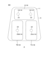
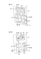
図2は、図1の導子2の模式的な正面図である。図3は、図1の導子2の模式的な背面図(第1形態)である。図4は、図1の導子2の模式的な背面図(第2形態)である。図5は、図1の導子2の模式的な背面図(第3形態)である。次に、前述の電気刺激装置1に使用可能な導子2の一例を示す。図6および図7は、それぞれ、図5の電極配線21のパターンの第1変形例および第2変形例を示す図である。
[導子の構成]
図2は、図1の導子2の模式的な正面図である。図3は、図1の導子2の模式的な背面図(第1形態)である。図4は、図1の導子2の模式的な背面図(第2形態)である。図5は、図1の導子2の模式的な背面図(第3形態)である。次に、前述の電気刺激装置1に使用可能な導子2の一例を示す。図6および図7は、それぞれ、図5の電極配線21のパターンの第1変形例および第2変形例を示す図である。
導子2は、シート基材5と、不関電極6および一対の刺激電極7A,7Bとを含む。
シート基材5は、人体10が屈曲(可動)したときに、その屈曲に合わせて湾曲可能な可撓性を有する材料からなる。この実施形態では、シート基材5は、絶縁性を有し、かつ人体10の表面に押し当てられる第1面11および第1面11の反対側の第2面12を有する平面形状のシート部材で構成されている。シート基材5の形状は、この実施形態では、角部がラウンド形状である長方形状(図3および図5~図7)や略三角形状(図4)であるが、特に制限されず、人体10における電気刺激の対象部位の形状に応じて適宜変更することができる。例えば、シート基材5の形状は、正方形状、円形状等であってもよい。
シート基材5の材料としては、例えば、樹脂フィルム、不織布、紙等の絶縁材料が挙げられる。これらは、単独または2種以上組み合わせて使用されてもよい。この実施形態では、シート基材5は、紙からなる。使用される紙としては、例えば、木材パルプやコットンパルプ等の天然素材を原料とする天然紙、合成樹脂パルプ等の合成樹脂素材を原料とする合成紙、天然素材および合成樹脂素材の混合素材を原料とする混合紙のいずれであってもよい。
シート基材5が紙製であれば、一定期間使用した後に廃棄されるディスポーザブル品としての導子2を提供することができる。例えば、電気刺激装置1によって適切な刺激効果を得るためには、電気刺激装置1に適した導電性シート8,9A,9B(導電性ゲル)を使用する必要がある。例えば、粘着面へのゴミや埃等の付着によって、導電性ゲルの電気抵抗値が上昇し、十分な電気刺激を人体に出力することが困難になる場合がある。そのため、導電性ゲルは定期的に交換されることが好ましい。導子2がディスポーザブル品であれば、導電性ゲルの交換時に導電性ゲルだけを取り外さなくても、導電性ゲルと一緒に導子2を廃棄することができる。そのため、電気刺激装置1を日常的に使用する場合に、導電性ゲルの交換作業が不要になる。特に、高齢者にとっては導電性ゲルの位置合わせを含む交換作業が大変なので、使用する際の負担が軽減される。
また、シート基材5の厚さは、電気刺激用の導子2としての使用に耐えることができる強度を有していれば特に制限されないが、例えば、0.05mm~5mmであってもよい。
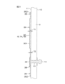
シート基材5の第2面12には、接続部の一例としての第1端子19および第2端子20A,20Bが設けられている。第1端子19および第2端子20A,20Bは、この実施形態では、スナップ端子13である。図8を参照して第1端子19の構造を具体的に説明する。第2端子20A,20Bの具体的な構造は第1端子19と同じであるため詳細な説明を省略する。
スナップ端子13は、シート基材5を挟むように固定されており、シート基材5の第1面11および第2面12の両面に露出している。スナップ端子13は、この実施形態では、雄型端子であり、シート基材5の第2面12から突出するスタッド部14を有している。このスタッド部14が外部接続用の端子部として使用され、配線コード4を介して電気刺激装置1に電気的に接続される。配線コード4の先端には、例えば樹脂製のカバー15で覆われたスナップ端子16(雌型端子)が設けられている。スナップ端子16には凹部17が形成されている。凹部17にスタッド部14が嵌合することによって、スナップ端子16がスナップ端子13にスナップ結合される。
スナップ端子13の数は、特に制限されない。図2では、一例として、不関電極6側に2つのスナップ端子13が設けられ、一対の刺激電極7A,7B側には、それぞれスナップ端子13が1つずつ設けられている。
なお、第1端子19および第2端子20A,20Bと配線コード4の接続は、前述のスナップ結合に限らず、例えば、差し込み結合であってもよい。例えば、配線コード4の先端に差込式コネクタ(雄型)を設け、第1端子19および第2端子20A,20Bにその差込口を設けてもよい。例えば、磁石を引き付ける導電性金属により第1端子19および第2端子20A,20Bを形成し、配線コード4の先端に、磁力により第1端子19および第2端子20A,20Bとの間の接触力を維持するコネクタを設けてもよい。
シート基材5の第1面11には、不関電極6および一対の刺激電極7A,7Bがそれぞれ形成されている。以下では、図3~図7を参照して、不関電極6および一対の刺激電極7A,7Bの第1形態~第3形態をそれぞれ説明する。なお、不関電極6および一対の刺激電極7A,7Bの形態は図3~図7の構造に制限されない。例えば、不関電極6のみに図3の第1形態が選択的に適用され、一対の刺激電極7A,7Bには図5~図7の第3形態が適用されてもよい。
図3および図4を参照して、不関電極6および一対の刺激電極7A,7Bは、導電層の一例としての導電性ゴム層18により形成されていてもよい。導電性ゴム層18は、この実施形態では、カーボンブラック等の導電性カーボンを含有するシリコーンゴム層により形成されている。導電性ゴム層18の材料としては、導電性を有するゴムであれば、カーボンブラックを含有するシリコーンゴムに限らない。例えば、シリコーンゴムに混入する導体(導電性充填剤)としては、カーボンブラックの他、銀粉末、金メッキされたシリカやグラファイト、導電性亜鉛華等であってもよい。また、イオン導電性シリコーンゴムを、導電性ゴム層18の材料として使用してもよい。
導電性ゴム層18は、シート基材5の第1面11の一定領域を覆う平面形状に形成されている。ここで「一定領域を覆う平面形状」とは、例えば、シート基材5の第1面11において一定の広さを有する部分を全体的に覆う形状である。また、平面視において、正方形、長方形、三角形、円形等で定義でき、ライン状の配線とは区別される形状であってもよい。この実施形態では、導電性ゴム層18は、第1面11から露出するスナップ端子13の導通点22に接触して覆う長方形状に形成されている。導電性ゴム層18は、導通点22を介してスナップ端子13に電気的に接続される。導電性ゴム層18の形状は、この実施形態では長方形状であるが、特に制限されず、人体10における電気刺激の対象部位の形状に応じて適宜変更することができる。例えば、導電性ゴム層18の形状は、正方形状、円形状、三角形状等であってもよい。
また、導電性ゴム層18の厚さは特に制限されないが、例えば、10μm~5000μmであってもよい。導電性ゴム層18は、例えば、導電性カーボンが分散した分散液をシート基材5の第1面11に所定の形状で塗り、固化させることによって形成することができる。
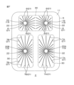
導電性ゴム層18とは異なる形態として、図5~図7を参照して、不関電極6および一対の刺激電極7A,7Bは、ライン状の電極配線21により形成されていてもよい。電極配線21は、この実施形態では、所定幅を有する導線によって形成されていてもよい。電極配線21の材料としては、例えば、銀、銅等が挙げられ、この実施形態では、銀塩化銀(AgAgCl)配線が使用されている。
電極配線21は、シート基材5の第1面11の一定領域内において、スナップ端子13との導通点22(例えば、シート基材5の第1面11から露出したスナップ端子13の部分)の周囲に張り巡らされている。ここで、「第1面11の一定領域」は、人体10における電気刺激の対象部位に接触させるべき領域であり、例えば、導電性シート8,9A,9Bとほぼ一致する形状の領域であってもよい。したがって、電極配線21が形成される領域は、ゲル配置領域30と定義してもよい。図5~図7では、ゲル配置領域30が二点鎖線からなる仮想線で示されている。
また、「導通点22の周囲に張り巡らされている」は、電極配線21が導通点22から導通点22の周囲の全体に延びていると定義してもよい。したがって、電極配線21は、図5に示すように、導通点22の一箇所を起点として導通点22を取り囲む1本のラインで螺旋状のパターンに形成されていてもよい。また、電極配線21は、図6に示すように、導通点22の複数箇所から延びる複数本の互いに独立したラインにより形成され、各ラインが葛折り状のパターンとなるように往復することによってゲル配置領域30の全体に張り巡らされていてもよい。さらに、葛折り状のパターンに変えて、電極配線21は、図7に示すように、導通点22の複数箇所から延びる放射線状のパターンで形成されていてもよい。電極配線21をこのように形成することによって、電極配線21は、互いに間隔を空けて並ぶパターンを有している。また、電極配線21は、導通点22を介してスナップ端子13に電気的に接続される。
電極配線21の幅は特に制限されないが、例えば、0.5mm~10mmであってもよい。また、電極配線21の厚さは特に制限されないが、例えば、10μm~5000μmであってもよい。また、電極配線21の間隔(ピッチ)は特に制限されないが、例えば、0.5mm~10mmであってもよい。電極配線21は、例えば、導電性物質を含有する導電性インク(例えば、銀塩化銀インク、銅インク等)をシート基材5の第1面11に所定の配線パターンで印刷し、固化させることによって形成することができる。
[機器本体の構成]
図9は、図1の機器本体3の模式的な正面図である。図10は、図1の機器本体3の模式的な背面図である。図11は、図1の機器本体3の模式的な平面図である。
[機器本体の構成]
図9は、図1の機器本体3の模式的な正面図である。図10は、図1の機器本体3の模式的な背面図である。図11は、図1の機器本体3の模式的な平面図である。
機器本体3は、携帯型の電気刺激治療装置である。機器本体3は、筐体23と、筐体23の前面に設けられたモニタ24と、モニタ24の下方に設けられたスタート/ストップボタン25および複数の操作ボタン26とを含む。
筐体23は、この実施形態では、略楕円形状に形成され、例えば、プラスチック製のケースからなっていてもよい。筐体23の上面には、第1差込口27と、第2差込口28とが設けられている。
第1差込口27は、例えば出力用のポートであり、配線コード4が接続される。一方、第2差込口28は、例えば充電用のポートであり、ACアダプタ(図示せず)のコードが接続される。つまり、機器本体3は、充電した電池やACアダプタを介してコンセントから供給される電源によってオンにすることができる。
モニタ24は、筐体23の長手方向に沿って長い長方形状に形成され、筐体23の長手方向の一端部寄りに配置されていてもよい。また、モニタ24は、例えば、モノクロもしくはカラーの液晶モニタであってよい。モニタ24には、例えば、一対の刺激電極7A,7Bによる電気的な刺激信号のパルス波形や周波数、被治療者の心電波形および心拍数、被治療者に知らせるべきメッセージ等を表示することができる。これにより、被治療者は、電気刺激装置1の動作状態を容易に知ることができる。モニタ24は、例えば、所定の操作画面が表示され、当該画面を操作可能なタッチパネルであってもよい。
スタート/ストップボタン25および複数の操作ボタン26は、モニタ24に対して、筐体23の長手方向他端部側に配置されていてもよい。また、操作ボタン26は、電気刺激装置1の機種によって、様々な機能を有していてもよい。例えば、電気刺激装置1のメモリ機能として、複数の被治療者それぞれに適した刺激信号のパルス波の幅(パルス幅)、周波数等を含む治療メニューを機器本体3に記憶させておき、それを読み出す際に操作するボタン等であってもよい。
また、機器本体3には、読み取り器29が内蔵されている。読み取り器29は、例えば、図9に示すように、モニタ24に対して筐体23の長手方向他端部側に内蔵されていてもよいし、図10に示すように、モニタ24の背面側に内蔵されていてもよい。読み取り器29は、例えば、RFID(Radio Frequency IDentifier)に使用されるRFタグを読み取るリーダを含んでいてもよい。
なお、機器本体3は、図12に示す変形例の構成であってもよい。図12を参照して、機器本体3は、設置型の電気刺激治療装置である。機器本体3は、例えば病院等の施設に常時設置された状態で使用される。機器本体3は、物理的な構成として、筐体58と、モニタ59と、電源ボタン60と、操作ボタン61と、ポート62とを備えている。
筐体58は、この実施形態では、略長方形状に形成され、例えば、プラスチック製のケースからなっていてもよい。図示しないが、筐体58の背面には、ACアダプタ等の接続用の差込口が設けられていてもよい。
モニタ59は、筐体58の前面に設けられている。モニタ59は、筐体58の長手方向に沿って長い長方形状に形成されていてもよい。モニタ59は、例えば、モノクロもしくはカラーの液晶モニタであってよい。例えば、一対の刺激電極7A,7Bによる電気的な刺激信号のパルス波形や周波数、被治療者の心電波形および心拍数、被治療者に知らせるべきメッセージ等を表示することができる。これにより、被治療者は、電気刺激装置1の動作状態を容易に知ることができる。モニタ59は、例えば、所定の操作画面が表示され、当該画面を操作可能なタッチパネルであってもよい。
電源ボタン60および操作ボタン61は、例えばモニタ59の下方に設けられている。操作ボタン61は、機器本体3の機種によって、様々な機能を有していてもよい。例えば、機器本体3のメモリ機能として、複数の被治療者それぞれに適した刺激信号のパルス波の幅(パルス幅)、周波数等を含む治療メニューを機器本体3に記憶させておき、それを読み出す際に操作するボタン等であってもよい。
ポート62は、筐体58の前面に複数設けられている。各ポート62には、配線コード4を介して導子2が1つずつ接続される。ポート62に導子2を1つずつ接続することによって、複数の被治療者が同時に、電気刺激治療を受けることができる。
[シート基材へのスリットの形成]
例えば、特許文献1に記載の発明において、不関電極および刺激電極は全体が平坦なシート状に形成されている。そのため、生体表面に貼付したときに電極の貼付面の一部がぴったりと貼り付かず、シートにしわが寄る場合がある。これにより、シートと生体表面との間に気泡等の空間が形成され、生体表面に効率よく電気刺激を伝達できない場合がある。その結果、十分な電気刺激を生体に出力することができず、電気刺激による十分な効果を得ることができない場合がある。
[シート基材へのスリットの形成]
例えば、特許文献1に記載の発明において、不関電極および刺激電極は全体が平坦なシート状に形成されている。そのため、生体表面に貼付したときに電極の貼付面の一部がぴったりと貼り付かず、シートにしわが寄る場合がある。これにより、シートと生体表面との間に気泡等の空間が形成され、生体表面に効率よく電気刺激を伝達できない場合がある。その結果、十分な電気刺激を生体に出力することができず、電気刺激による十分な効果を得ることができない場合がある。
そこで、この実施形態では、シート基材5を立体的に変形させるためのスリット31,32,33が形成されている。以下では、スリット31~33のパターンのバリエーションを図13~図16を参照して説明する。
図13は、導子2に形成されたスリット31(第1パターン)を説明するための図である。図13は、図3に対応する図であり、不関電極6および一対の刺激電極7A,7Bは導電性ゴム層18により形成されている。図13では、便宜上、導子2の幅方向(横方向)を第1方向Xと定義し、導子2の長さ方向(縦方向)を第2方向Yと定義する。第2方向Yは、第1方向Xに直交する方向である。
図13の導子2では、スリット31は、シート基材5のほぼ全面に形成されている。スリット31は、シート基材5に複数形成されている。この実施形態では、スリット31は、第1方向Xに延びる直線状の第1スリット311と、第2方向Yに延びる直線状の第2スリット312とを含む。第1スリット311および第2スリット312は、シート基材5に規則的に配置されている。より具体的には、第1方向Xおよび第2方向Yに沿って、第1スリット311および第2スリット312が交互に配列されている。複数の第1スリット311は、第1方向Xおよび第2方向Yにおいて互いに隣り合わないように、千鳥状に配列されている。同様に、複数の第2スリット312は、第1方向Xおよび第2方向Yにおいて互いに隣り合わないように、千鳥状に配列されている。
各第1スリット311および各第2スリット312は、それぞれ、第1端部311A,312Aおよびその反対側の第2端部311B,312Bを有している。いくつかの第1スリット311および第2スリット312は、シート基材5において導電性ゴム層18が形成されていない領域において、シート基材5を貫通するように形成されていてもよい。また、他のいくつかの第1スリット311および第2スリット312は、シート基材5において導電性ゴム層18が形成されている領域において、導電性ゴム層18に重なるように形成されていてもよい。したがって、いくつかの第1スリット311および第2スリット312は、導電性ゴム層18およびシート基材5を連続して貫通していてもよい。
導電性ゴム層18に重なる各第1スリット311および各第2スリット312は、少なくとも一方の端部311A,312A,311B,312Bが導電性ゴム層18の外周縁181よりも内側に配置されている。これにより、導電性ゴム層18がスリット31によって分断されていない。したがって、スナップ端子13と導電性ゴム層18との電気的な接続を導電性ゴム層18の全体にわたって確保することができる。
図14は、導子2に形成されたスリット32(第2パターン)を説明するための図である。図15は、図14のスリット32の配置方向の変形例を示す図である。図14および図15は、図3に対応する図であり、不関電極6および一対の刺激電極7A,7Bは導電性ゴム層18により形成されている。図14では、便宜上、導子2の幅方向(横方向)に対して45°傾斜した方向を第1方向Xと定義し、第1方向Xに直交する方向を第2方向Yと定義する。
図14の導子2では、スリット32は、シート基材5のほぼ全面に形成されている。スリット32は、シート基材5に複数形成されている。この実施形態では、スリット32は、第1方向Xに延びる直線状の第1スリット321と、第2方向Yに延びる直線状の第2スリット322とを含む。第1スリット321および第2スリット322は、シート基材5に規則的に配置されている。より具体的には、複数のスリット32はそれぞれ、第1スリット321および第2スリット322が十字に交差することによって十字スリットとして形成されている。そして、複数の十字スリット32は、シート基材5に行列状に配列されている。複数の十字スリット32の向きは、図14に示すようにXパターンであってもよいし、図15に示すように十字パターンであってもよい。
各第1スリット321および各第2スリット322は、それぞれ、第1端部321A,322Aおよびその反対側の第2端部321B,322Bを有している。いくつかの第1スリット321および第2スリット322は、シート基材5において導電性ゴム層18が形成されていない領域において、シート基材5を貫通するように形成されていてもよい。また、他のいくつかの第1スリット321および第2スリット322は、シート基材5において導電性ゴム層18が形成されている領域において、導電性ゴム層18に重なるように形成されていてもよい。したがって、いくつかの第1スリット321および第2スリット322は、導電性ゴム層18およびシート基材5を連続して貫通していてもよい。
導電性ゴム層18に重なる各第1スリット321および各第2スリット322は、少なくとも一方の端部321A,322A,321B,322Bが導電性ゴム層18の外周縁181よりも内側に配置されている。これにより、導電性ゴム層18がスリット32によって分断されていない。したがって、スナップ端子13と導電性ゴム層18との電気的な接続を導電性ゴム層18の全体にわたって確保することができる。
図16は、導子2に形成されたスリット33(第3パターン)を説明するための図である。図16は、図5に対応する図であり、不関電極6および一対の刺激電極7A,7Bは電極配線21により形成されている。図16では、便宜上、導子2の幅方向(横方向)を第1方向Xと定義し、導子2の長さ方向(縦方向)を第2方向Yと定義する。第2方向Yは、第1方向Xに直交する方向である。また、スリット33と電極配線21との区別を明瞭化するため、電極配線21の巻き数を減らし、電極配線21の間隔を広げている。
図16の導子2では、複数のスリット33が、隣り合う電極配線21の間の領域34に形成されている。この実施形態では、電極配線21が螺旋状に形成されているので、領域34は、第1方向Xに延びる第1領域341と、第2方向Yに延びる第2領域342とを含んでいてもよい。複数のスリット33は、第1領域341に形成された第1スリット331と、第2領域342に形成された第2スリット332とを含む。
第1スリット331および第2スリット332は、それぞれ、電極配線21を横切らないように電極配線21に沿って形成されている。図16では、第1スリット331および第2スリット332は、電極配線21に平行に形成されている。これにより、電極配線21がスリット33によって分断されていない。したがって、スナップ端子13と電極配線21との電気的な接続を電極配線21の全体にわたって確保することができる。
ここで、スリット31~33の共通事項の説明を加える。スリット31~32は、シート基材5の1つだけ形成されていてもよいが、導子2をより柔軟に変形させる観点から複数形成されていることが好ましい。スリット31~33の数は特に制限されない。また、各スリット31~33の寸法(長さ)は、例えば、0.25cm~10cmであってもよい。また、隣り合うスリット31~33の間隔は、スリット31~33からシート基材5が裂けてスリット31~33同士が繋がることを防止する観点から、例えば、0.25cm~1.5cmであることが好ましい。
図17Aおよび図17Bは、スリット31が開口した状態を示す図である。次に、スリット31~33による導子2の立体的な変形を、スリット31に関連する図を参照して説明する。図17Aおよび図17Bは、図13の導子2が変形した後の状態を示す図であるが、スリット31の開口状態を明瞭に示すためにスリット31の数を減らしている。
図13~図16に示したように、シート基材5にスリット31~33が形成されているので、スリット31~33が開口することによって生体表面の形状に合わせてシート基材5を立体的に変形させることができる。これにより、導子2を生体表面に良好にフィットさせることができる。
また、図13に示すように第1スリット311および第2スリット312が交互に配列されていれば、第1スリット311および第2スリット312をシート基材5の表面の領域ごとに偏らせず、満遍なく配置することができる。その結果、生体表面の形状に合わせてシート基材5を柔軟に変形させることができる。また、図14に示すように、スリット32が十字スリットであれば、十字スリット32の中心からその周囲に向かうあらゆる方向の変形に柔軟に対応することができる。
また、シート基材5の導電性ゴム層18や電極配線21に導電性シート8,9A,9B(導電性ゲル)を貼着して導子2を使用する場合、導電性シート8,9A,9Bと導電性ゴム層18や電極配線21との間に気泡が発生することがある。この場合、導電性シート8,9A,9Bの外周縁からだけでなく、複数のスリット31~33を介しても気泡を排除することができる。その結果、導電性シート8,9A,9Bと導電性ゴム層18や電極配線21との密着性を向上できる(接触面積を大きく確保できる)ので、導電性ゴム層18や電極配線21から導電性シート8,9A,9Bを介して、生体表面に効率よく電気刺激を伝達することができる。
さらに、複数のスリット31~33の間には、スナップ端子13と導電性ゴム層18(または、スナップ端子13と電極配線21)との電気的な接続を確保する領域が形成されている。これにより、生体表面に電気刺激を伝達するための領域として、導電性ゴム層18および電極配線21の全体を有効に利用することができる。
[電極の導電性コントロール]
例えば、特許文献1に記載の発明において、不関電極および刺激電極は全体が平坦なシート状に形成されている。そのため、シート表面に沿う方向において電気抵抗が均等となり、電気刺激が強く必要な箇所では電圧・電流が不足し、電気刺激がそれほど必要ではない箇所では過剰な電圧・電流が供給される場合がある。
[電極の導電性コントロール]
例えば、特許文献1に記載の発明において、不関電極および刺激電極は全体が平坦なシート状に形成されている。そのため、シート表面に沿う方向において電気抵抗が均等となり、電気刺激が強く必要な箇所では電圧・電流が不足し、電気刺激がそれほど必要ではない箇所では過剰な電圧・電流が供給される場合がある。
そこで、この実施形態では、不関電極6および一対の刺激電極7A,7Bが、電圧・電流の大きさが互いに異なる分布を有している。以下では、不関電極6および一対の刺激電極7A,7Bの電圧・電流の分布のバリエーションを図18~図23を参照して説明する。
図18は、導電性ゴム層18における厚さ分布(第1パターン)を示す図である。図19は、図18のXIX-XIX線における断面図である。図18および図19は、図3に記載の刺激電極7Aを選択的に示している。図18に示す導電性ゴム層18の厚さ分布は刺激電極7Aに限らず不関電極6および刺激電極7Bにも適用できるため、図18では便宜上、不関電極6および刺激電極7A,7Bを総称して電極35と定義する。
図18の電極35に係る導電性ゴム層18は、第1厚さT1を有する第1部分351と、第1厚さT1よりも小さな第2厚さT2を有する第2部分352とを含む。相対的に厚い第1部分351では、相対的に薄い第2部分352に比べて電流の経路が広くなるので抵抗が小さくなる。例えば、第1部分351の抵抗値(第1抵抗値)は、5Ω~10Ωであり、第2部分352の抵抗値(第2抵抗値)は、10Ω~50Ωであってもよい。また、第1厚さT1は、例えば50μm~500μmであり、第2厚さT2は、例えば10μm~50μmであってもよい。さらに、第1部分351から第2部分352の間で、5Ω~50Ω、10μm~500μmの範囲で連続的に変化していてもよい。
このように、導電性ゴム層18が互いに抵抗値が異なる第1部分351および第2部分352を含むので、導子2が貼付される生体部位に応じて、電圧・電流分布を柔軟に調整することができる。例えば、電圧・電流分布の調整のために導電性ゴム層18に所定パターンの導電材を別途形成したり埋め込んだりする必要がなくなるので、導子2の構造をシンプルにすることができる。また、第1部分351および第2部分352は、導電性ゴム層18を形成する際に塗工液(この実施形態では、導電性カーボンが分散した分散液)の塗り量を場所ごとに分けることによって簡単に形成することができる。
この実施形態では、導電性ゴム層18の第2部分352は導電性ゴム層18の外周縁部36に形成され、導電性ゴム層18の第1部分351は、外周縁部36よりも内側の中央領域37に形成されている。外周縁部36は、例えば、導電性ゴム層18の外周縁181(導電性ゴム層18の輪郭ライン)から内側に向かって0.5cmまでの部分であってもよい。中央領域37は、外周縁部36で囲まれた領域であってもよい。なお、第1部分351と第2部分352との境界は定規で線を引いたように直線状ではないため、図18では、第1部分351が形成された大まかな領域をハッチングで示し、第2部分352が形成された領域をハッチングの周囲の白色の領域で示している。
この実施形態のように導子2の基材がシート基材5であるため、例えば、導子2を生体表面に貼付したときに導電性ゴム層18の外周縁部36の一部が生体表面から浮いた状態となる。この状態で導子2から生体表面に電気刺激を与えると、導電性ゴム層18の外周縁部36の近傍でチクチクする痛みを感じる場合がある。そこで、図18の構成によれば、相対的に高い第2抵抗値を有する第2部分352を導電性ゴム層18の外周縁部36に配置することによって、導電性ゴム層18の外周縁部36の抵抗値を高くして当該部分での電圧・電流の大きさを小さくすることができる。これにより、導電性ゴム層18の外周縁部36の一部が浮いていても、チクチクする痛みのような不快感を軽減することができる。
図20は、導電性ゴム層18における厚さ分布(第2パターン)を示す図である。図21は、図20のXXI-XXI線における断面図である。図20および図21では、図18と同様に、便宜上、不関電極6および刺激電極7A,7Bを総称して電極35と定義する。また、図18と図20および図21との間で共通する構成要素には同じ参照符号を付し、その説明を省略する。
この実施形態では、導電性ゴム層18の第2部分352は導電性ゴム層18とスナップ端子13との導通点22の周囲の端子近傍領域38に形成され、導電性ゴム層18の第1部分351は、第2部分352のさらに周囲であり、スナップ端子13から離れた端子離隔領域39に形成されている。端子近傍領域38は、例えば、スナップ端子13から5cmまでの周囲部分であってもよい。また、端子近傍領域38は、スナップ端子13の周囲の外周部分であって、導電性ゴム層18の外周縁181までの幅が最も小さい幅の部分の半分までの領域であってもよい。端子離隔領域39は、端子近傍領域38から導電性ゴム層18の外周縁181までの領域であってもよい。なお、図20の構造においても図18と同様に、第2部分352は導電性ゴム層18の外周縁部36にも形成されている。
この構成によれば、相対的に高い第2抵抗値を有する第2部分352を、比較的電圧・電流が集中し易い導通点22の近傍に配置することによって、導電性ゴム層18の全体にわたって電圧・電流分布の均一化を図ることができる。
図22は、電極配線21の密集状態を示す図である。図22は、図5に記載の刺激電極7Aを選択的に示している。図22に示す電極配線21の密集状態は刺激電極7Aに限らず不関電極6および刺激電極7Bにも適用できるため、図22では便宜上、不関電極6および刺激電極7A,7Bを総称して電極40と定義する。
図22では、電極配線21が第1間隔W1で並んで形成された密パターン領域41と、電極配線21が第1間隔W1よりも広い第2間隔W2で並んで形成された疎パターン領域42とが形成されている。密パターン領域41は、疎パターン領域42に比べて電極配線21が密集した領域である。例えば、互いに同じ単位長さを有する単位領域43を横切る電極配線21の本数が、密パターン領域41の方が疎パターン領域42よりも多くなっている。例えば図22では、疎パターン領域42の単位領域43を横切る電極配線21が2本であるのに対して、密パターン領域41の単位領域43を横切る電極配線21は、6本となっている。
相対的に電極配線21が密集した密パターン領域41では、疎パターン領域42に比べて電流の経路が多くなるので抵抗が小さくなる。つまり、電極配線21は、相対的に低い第1抵抗値を有する第1部分401と、第1抵抗値よりも高い第2抵抗値を有する第2部分402とを含む。例えば、第1部分401の抵抗値(第1抵抗値)は、5Ω~10Ωであり、第2部分402の抵抗値(第2抵抗値)は、10Ω~50Ωであってもよい。また、密パターン領域41における電極配線21の第1間隔W1は、例えば0.5mm~5mmであり、疎パターン領域42における電極配線21の第2間隔W2は、例えば5mm~10mmであってもよい。さらに、電極配線21の密パターン領域41の第1間隔W1から疎パターン領域42の第2間隔W2まで、0.5mm~10mmの範囲で連続的に変化していてもよい。
この実施形態では、電極配線21の第2部分402はゲル配置領域30の外周縁部44に形成され、電極配線21の第1部分401は、外周縁部44よりも内側の中央領域45に形成されている。外周縁部44は、例えば、ゲル配置領域30の外周縁301(配置される導電性ゲルの外周縁が位置すると想定されるライン)から内側に向かって0.5cmまでの部分であってもよい。中央領域45は、外周縁部44で囲まれた領域であってもよい。
図22の構成によれば、相対的に高い第2抵抗値を有する第2部分402をゲル配置領域30の外周縁部44に配置することによって、ゲル配置領域30の外周縁部44の抵抗値を高くして当該部分での導電性ゲルの電圧・電流の大きさを小さくすることができる。これにより、ゲル配置領域30(導電性ゲル)の外周縁部44の一部が浮いていても、チクチクする痛みのような不快感を軽減することができる。また、第1部分401および第2部分402は、電極配線21を形成する際に導電性インクの印刷パターンを設定するだけで簡単に区別して形成することができる。
なお、図示は省略するが、図20に倣って、端子近傍領域38に疎パターン領域42を形成し、端子離隔領域39に密パターン領域41を形成することによって、電極配線21の全体にわたって電圧・電流分布の均一化を図ることができる。
図23は、電極配線21の密集状態の別の形態を示す図である。図23は、図5に記載の刺激電極7Aを選択的に示している。図23に示す電極配線21の密集状態は刺激電極7Aに限らず不関電極6および刺激電極7Bにも適用できるため、図23では便宜上、不関電極6および刺激電極7A,7Bを総称して電極40と定義する。
図23では、電極配線21が一定の間隔(ピッチ)P1で螺旋状に形成されている。電極配線21は、第1幅W1を有する配線により形成された密パターン領域63と、第1幅W1よりも狭い第2幅W2を有する配線により形成された疎パターン領域64とが形成されている。この幅の相違により、密パターン領域63は、疎パターン領域64に比べて電極配線21が密集した領域である。例えば、互いに同じ単位長さを有する単位領域43を横切る電極配線21の面積が、密パターン領域63の方が疎パターン領域64よりも大きくなっている。
相対的に電極配線21が密集した密パターン領域63では、疎パターン領域64に比べて電流の経路が太くなるので抵抗が小さくなる。つまり、電極配線21は、相対的に低い第1抵抗値を有する第1部分403と、第1抵抗値よりも高い第2抵抗値を有する第2部分404とを含む。例えば、第1部分403の抵抗値(第1抵抗値)は、5Ω~10Ωであり、第2部分404の抵抗値(第2抵抗値)は、10Ω~50Ωであってもよい。
この実施形態では、電極配線21の第2部分404はゲル配置領域30の外周縁部44に形成され、電極配線21の第1部分403は、外周縁部44よりも内側の中央領域45に形成されている。外周縁部44は、例えば、ゲル配置領域30の外周縁301(配置される導電性ゲルの外周縁が位置すると想定されるライン)から内側に向かって0.5cmまでの部分であってもよい。中央領域45は、外周縁部44で囲まれた領域であってもよい。
図23の構成によれば、相対的に高い第2抵抗値を有する第2部分404をゲル配置領域30の外周縁部44に配置することによって、ゲル配置領域30の外周縁部44の抵抗値を高くして当該部分での導電性ゲルの電圧・電流の大きさを小さくすることができる。これにより、ゲル配置領域30(導電性ゲル)の外周縁部44の一部が浮いていても、チクチクする痛みのような不快感を軽減することができる。また、第1部分403および第2部分404は、電極配線21を形成する際に導電性インクの印刷パターンを設定するだけで簡単に区別して形成することができる。
なお、図示は省略するが、図20に倣って、端子近傍領域38に疎パターン領域64を形成し、端子離隔領域39に密パターン領域63を形成することによって、電極配線21の全体にわたって電圧・電流分布の均一化を図ることができる。
[端子の切り離し構造]
例えば、導子2が紙製のシート基材5を備えるディスポーザブル品である場合、導子を一定期間使用した後、導子2はそのまま廃棄される。しかしながら、導子2には、紙により形成された可燃性のシート基材5と、金属により形成された難燃性のスナップ端子13とが混在しているため、スナップ端子13を取り外して分別する必要がある。
[端子の切り離し構造]
例えば、導子2が紙製のシート基材5を備えるディスポーザブル品である場合、導子を一定期間使用した後、導子2はそのまま廃棄される。しかしながら、導子2には、紙により形成された可燃性のシート基材5と、金属により形成された難燃性のスナップ端子13とが混在しているため、スナップ端子13を取り外して分別する必要がある。
そこで、この実施形態では、スナップ端子13の周囲に易分離加工部46が形成されている。図24は、シート基材5の易分離加工部46を説明するための図である。
易分離加工部46は、シート基材5の一部を選択的に加工することによって形成された部分であり、スナップ端子13を容易に分離することを提供する。易分離加工部46は、スナップ端子13を取り囲むように形成されている。好ましくは、易分離加工部46は、スナップ端子13のほぼ全周を取り囲んでいる。
易分離加工部46の構造は特に制限されないが、この実施形態では、スナップ端子13を取り囲むように形成されたミシン目ライン47である。ミシン目ライン47の周方向の一部にはシート基材5から起き上がり可能な摘まみ48が形成されていてもよい。例えば、摘まみ48を持ち手前に引くことで、ミシン目ライン47で囲まれたシート基材5の一部(端子領域49とその周囲との間)がミシン目ライン47を境界にして引き裂かれる。これにより、スナップ端子13が端子領域49と共に、シート基材5から分離される。その結果、紙製のシート基材5と、金属製のスナップ端子13とを容易に分離でき、それぞれを分別して廃棄することができる。
なお、易分離加工部46はミシン目ライン47に限らず、例えば、シート基材5の一部をライン状(図24では、スナップ端子13を取り囲む円環状)に選択的に薄く形成することによって形成された引き裂きやすい部分であってもよい。
[装着サポータの構成]
図25は、装着サポータ50の模式的な斜視図である。図26は、装着サポータ50の模式的な斜視図である。図27Aおよび図27Bは、導子用パッド部51の変形前後の状態を示す図である。図28~図30は、装着サポータ50を使用して導子を装着した状態を示す図である。図28が人体10を正面側から見た図であり、図29が人体10を背面側から見た図であり、図30が人体10を左側面側から見た図である。
[装着サポータの構成]
図25は、装着サポータ50の模式的な斜視図である。図26は、装着サポータ50の模式的な斜視図である。図27Aおよび図27Bは、導子用パッド部51の変形前後の状態を示す図である。図28~図30は、装着サポータ50を使用して導子を装着した状態を示す図である。図28が人体10を正面側から見た図であり、図29が人体10を背面側から見た図であり、図30が人体10を左側面側から見た図である。
装着サポータ50は、導子2の装着を補助するデバイスである。装着サポータ50は、導子2を保持する導子保持部の一例としての導子用パッド部51と、導子用パッド部51に接続されたベルト52とを含む。装着サポータ50は、例えば布生地により形成された導子用パッド部51およびベルト52を一体的に有していてもよい。導子用パッド部51およびベルト52は、それぞれ別々のパーツとして形成された後、例えば縫製によって互いに接続されていてもよい。
導子用パッド部51は、装着サポータ50の中央に設けられている。導子用パッド部51は、例えば後方に凹んだ湾曲シート形状に形成されている。これにより、導子用パッド部51は、シート基材5の第2面12が接続される面が凹面53となっている。導子用パッド部51の平面形状は、この実施形態では導子2の形状に合わせて略長方形状であるが、円形状等の他の形状であってもよい。凹面53には、導子2を導子用パッド部51に固定するための固定具54が設けられている。固定具54は、導子2を固定できれば特に制限されないが、例えばスナップボタンであってもよい。
ベルト52は、左右に伸縮性を有しており、導子用パッド部51の左右両側に接続されている。ベルト52は、導子用パッド部51の左側(紙面右側)の左側ベルト52Lと、導子用パッド部51の右側(紙面左側)の右側ベルト52Rとを含む。左側ベルト52Lおよび右側ベルト52Rはそれぞれ、互いに上下に間隔を空けて設けられた2本ずつ設けられている。各ベルト52の先端には、ベルト52同士を固定する留め具55が設けられている。留め具55は、ベルト52同士が離れないように固定できれば特に制限されないが、例えば、面ファスナ、止め金具(フック)等であってもよい。
装着サポータ50を使用して導子2を装着するには、まず、図25を参照して、導子2の不関電極6および一対の刺激電極7A,7Bに、導電性シート8,9A,9B(導電性ゲル)が貼着される。次に、固定具54を介して導子2が導子用パッド部51に固定される。図26に示すように、導子2は、導子用パッド部51の凹面53に沿って窪んだ形状で保持される。この際、シート基材5にスリット31(図17Aおよび図17B参照)が形成されていればスリット31が開口して導子2が立体的に変形するため、導子2が突っ張ることを抑制し凹面53に沿って簡単に窪ませることができる。これにより、導電性シート8,9A,9B(導電性ゲル)も凹面53に沿って窪ませた形状に変形させることができる。そのため、図27Aに示すように、導子2を人体10の表面に押し当てるまで、導電性ゲルが生体の電気刺激対象部位以外の表面や衣服等に不用意に粘着することを防止することができる。
次に、図27Aに示すように、装着サポータ50を使用して導子2の位置合わせをする。この実施形態では、導子2が仙骨の背面に収まるように位置合わせが行われる。この際、導子2が凹面53に沿って窪んでいるので、導子2と人体10の表面との間に空間57が形成されていてもよい。位置合わせ後、図26に示すようにベルト52を左右に引っ張って留め具55で固定する。これにより、図27Bに示すように、ベルト52が左右に引っ張られるとその動きに連動して導子用パッド部51(湾曲シート形状)が前方に向かって飛び出すように変形する。その結果、導子2を人体10の表面に簡単に押し当てることができる。なお、ベルト52の引っ張りだけでは導子2が人体10の表面に密着しない場合は、導子用パッド部51を後ろから押してもよい。
以上の作業を経て、図28~図29に示すように、導子2を装着することができる。そして、この実施形態では、左側ベルト52Lおよび右側ベルト52Rがそれぞれ、互いに上下に間隔を空けて2本ずつ設けられている。そのため、例えば腸骨稜56等の人体10の表面の出っ張りを上下のベルト52で挟むようにして装着サポータ50を固定することによって、装着サポータ50の位置ずれを抑制することができる。
本開示の実施形態について説明したが、本開示は他の形態で実施することもできる。
以上、本開示の実施形態は、すべての点において例示であり限定的に解釈されるべきではなく、すべての点において変更が含まれることが意図される。
この明細書および図面の記載から以下に付記する特徴が抽出され得る。
[付記1-1]
生体表面に押し当てられる第1面およびその反対側の第2面を有するシート状の絶縁材料により形成された基材と、
前記基材の前記第1面に導電性材料により形成された導電部と、
前記基材の前記第2面に形成され、前記導電部に導通する接続部と、
前記基材に形成された複数のスリットであって、前記複数のスリットの間には前記接続部と前記導電部との電気的な接続を確保する領域が形成されている複数のスリットとを含む、電気刺激用導子。
生体表面に押し当てられる第1面およびその反対側の第2面を有するシート状の絶縁材料により形成された基材と、
前記基材の前記第1面に導電性材料により形成された導電部と、
前記基材の前記第2面に形成され、前記導電部に導通する接続部と、
前記基材に形成された複数のスリットであって、前記複数のスリットの間には前記接続部と前記導電部との電気的な接続を確保する領域が形成されている複数のスリットとを含む、電気刺激用導子。
この構成によれば、基材がシート状であるため、電気刺激用導子を生体表面に貼付したときに、基材が生体表面の形状に沿おうとして基材に横方向(第1面および第2面に沿う方向)に力が加わる。この際、基材にスリットが形成されているので、スリットが開口することによって生体表面の形状に合わせてシート状の基材を立体的に変形させることができる。これにより、電気刺激用導子を生体表面に良好にフィットさせることができる。
また、基材の導電部に導電性ゲルを貼着して導子を使用する場合、導電性ゲルと導電部との間に気泡が発生することがある。この場合、導電性ゲルの外周縁からだけでなく、複数のスリットを介しても気泡を排除することができる。その結果、導電性ゲルと導電部との密着性を向上できる(接触面積を大きく確保できる)ので、導電部から導電性ゲルを介して、生体表面に効率よく電気刺激を伝達することができる。
さらに、複数のスリットの間には、接続部と導電部との電気的な接続を確保する領域が形成されている。これにより、生体表面に電気刺激を伝達するための領域として、導電部の全体を有効に利用することができる。
[付記1-2]
前記複数のスリットは、第1方向に延びる第1スリットと、前記第1方向に交差する方向に延びる第2スリットとを含む、付記1-1に記載の電気刺激用導子。
前記複数のスリットは、第1方向に延びる第1スリットと、前記第1方向に交差する方向に延びる第2スリットとを含む、付記1-1に記載の電気刺激用導子。
この構成によれば、複数の方向にスリットが開口するので、生体表面の形状に合わせて基材を柔軟に変形させることができる。
[付記1-3]
前記複数のスリットは、前記第1スリットおよび前記第2スリットが十字に交差することによって形成された十字スリットを含む、付記1-2に記載の電気刺激用導子。
前記複数のスリットは、前記第1スリットおよび前記第2スリットが十字に交差することによって形成された十字スリットを含む、付記1-2に記載の電気刺激用導子。
この構成によれば、十字スリットの中心で第1スリットおよび第2スリットが繋がっているので、十字スリットの中心からその周囲に向かうあらゆる方向の変形に柔軟に対応することができる。
[付記1-4]
前記複数のスリットは、前記第1スリットおよび前記第2スリットが交互に配列されることによって形成されている、付記1-2または付記1-3に記載の電気刺激用導子。
前記複数のスリットは、前記第1スリットおよび前記第2スリットが交互に配列されることによって形成されている、付記1-2または付記1-3に記載の電気刺激用導子。
この構成によれば、互いに開口方向が異なる第1スリットおよび第2スリットを基材表面の領域ごとに偏らせず、満遍なく配置することができる。その結果、生体表面の形状に合わせて基材を柔軟に変形させることができる。
[付記1-5]
前記導電部は、前記基材の前記第1面の一定領域を覆う平面形状に形成された導電層を含み、
前記複数のスリットは、前記導電層の外周縁よりも内側に少なくとも一端を有し、前記導電層および前記基材を連続して貫通するように形成されている、付記1-1~付記1-4のいずれか一項に記載の電気刺激用導子。
前記導電部は、前記基材の前記第1面の一定領域を覆う平面形状に形成された導電層を含み、
前記複数のスリットは、前記導電層の外周縁よりも内側に少なくとも一端を有し、前記導電層および前記基材を連続して貫通するように形成されている、付記1-1~付記1-4のいずれか一項に記載の電気刺激用導子。
この構成によれば、基材に加えて導電層にもスリットが形成されているので、スリットが開口することによって生体表面の形状に合わせて基材および導電層を共に立体的に変形させることができる。また、スリットの少なくとも一端が導電層の外周縁よりも内側に位置しているため、導電層がスリットによって分断されていない。これにより、接続部と導電層との電気的な接続を導電層の全体にわたって確保することができる。さらに、導電層が平面形状に形成されているため、基材における導電層が形成された領域の全体から生体表面に効率よく電気刺激を伝達することができる。
[付記1-6]
前記導電部は、前記基材の前記第1面の一定領域内において、前記接続部との導通点の周囲に張り巡らされた電極配線であって、互いに間隔を空けて並ぶパターンを有する電極配線を含み、
前記複数のスリットは、隣り合う前記電極配線の間の領域において前記電極配線に沿って形成されている、付記1-1~付記1-5のいずれか一項に記載の電気刺激用導子。
前記導電部は、前記基材の前記第1面の一定領域内において、前記接続部との導通点の周囲に張り巡らされた電極配線であって、互いに間隔を空けて並ぶパターンを有する電極配線を含み、
前記複数のスリットは、隣り合う前記電極配線の間の領域において前記電極配線に沿って形成されている、付記1-1~付記1-5のいずれか一項に記載の電気刺激用導子。
この構成によれば、基材における電極配線の間の領域にスリットが形成されているため、スリットと電極配線との間に一定に距離を確保することができる。これにより、電極配線と基材の第2面側との間の絶縁を良好に確保することができる。また、スリットが電極配線に沿って形成されているため、電極配線がスリットによって分断されていない。これにより、接続部と電極配線との電気的な接続を電極配線の全体にわたって確保することができる。
[付記1-7]
前記電極配線は、前記導通点を起点として螺旋状に形成されている、付記1-6に記載の電気刺激用導子。
前記電極配線は、前記導通点を起点として螺旋状に形成されている、付記1-6に記載の電気刺激用導子。
[付記1-8]
前記絶縁材料は合成紙を含む、付記1-1~付記1-7のいずれか一項に記載の電気刺激用導子。
前記絶縁材料は合成紙を含む、付記1-1~付記1-7のいずれか一項に記載の電気刺激用導子。
この構成によれば、電気刺激用導子をディスポーザブル品として提供することができ、廃棄される基材が合成紙を含むため、環境に与える負荷を軽減することもできる。
[付記1-9]
生体表面に押し当てられる第1面およびその反対側の第2面を有するシート状の絶縁材料により形成された基材と、
前記基材の前記第1面に導電性材料により形成された導電部と、
前記基材の前記第2面に形成され、前記導電部に導通する接続部とを含み、
前記導電部は、第1抵抗値を有する第1部分と、前記第1抵抗値よりも選択的に高く設定された所定範囲の第2抵抗値を有する第2部分とを含む、電気刺激用導子。
生体表面に押し当てられる第1面およびその反対側の第2面を有するシート状の絶縁材料により形成された基材と、
前記基材の前記第1面に導電性材料により形成された導電部と、
前記基材の前記第2面に形成され、前記導電部に導通する接続部とを含み、
前記導電部は、第1抵抗値を有する第1部分と、前記第1抵抗値よりも選択的に高く設定された所定範囲の第2抵抗値を有する第2部分とを含む、電気刺激用導子。
この構成によれば、導電部が互いに抵抗値が異なる第1部分および第2部分を含むので、電気刺激用導子が貼付される生体部位に応じて、電圧・電流分布を柔軟に調整することができる。例えば、電圧・電流分布の調整のために導電部に所定パターンの導電材を別途形成したり埋め込んだりする必要がなくなるので、電気刺激用導子の構造をシンプルにすることができる。
[付記1-10]
前記導電部は、前記基材の前記第1面の一定領域を覆う平面形状に形成された導電層を含み、
前記導電層は、第1厚さを有する前記第1部分と、前記第1厚さよりも小さな第2厚さを有する前記第2部分とを含む、付記1-9に記載の電気刺激用導子。
前記導電部は、前記基材の前記第1面の一定領域を覆う平面形状に形成された導電層を含み、
前記導電層は、第1厚さを有する前記第1部分と、前記第1厚さよりも小さな第2厚さを有する前記第2部分とを含む、付記1-9に記載の電気刺激用導子。
[付記1-11]
前記導電部は、前記基材の前記第1面の一定領域内において、前記接続部との導通点の周囲に張り巡らされた電極配線であって、互いに間隔を空けて並ぶパターンを有する電極配線を含み、
前記基材の前記第1面は、前記電極配線が第1間隔で並んで前記第1部分を形成する密パターン領域と、前記電極配線が前記第1間隔より広い第2間隔で並んで前記第2部分を形成する疎パターン領域とを含む、付記1-9に記載の電気刺激用導子。
前記導電部は、前記基材の前記第1面の一定領域内において、前記接続部との導通点の周囲に張り巡らされた電極配線であって、互いに間隔を空けて並ぶパターンを有する電極配線を含み、
前記基材の前記第1面は、前記電極配線が第1間隔で並んで前記第1部分を形成する密パターン領域と、前記電極配線が前記第1間隔より広い第2間隔で並んで前記第2部分を形成する疎パターン領域とを含む、付記1-9に記載の電気刺激用導子。
[付記1-12]
前記導電部は、前記基材の前記第1面の一定領域内において、前記接続部との導通点の周囲に張り巡らされた電極配線であって、異なる幅の電極配線を有するパターンを含み、
前記基材の前記第1面は、第1幅を有する前記電極配線で形成された密パターン領域と、前記第1幅よりも狭い第2幅を有する前記電極配線で形成された疎パターン領域とを含む、付記1-9に記載の電気刺激用導子。
前記導電部は、前記基材の前記第1面の一定領域内において、前記接続部との導通点の周囲に張り巡らされた電極配線であって、異なる幅の電極配線を有するパターンを含み、
前記基材の前記第1面は、第1幅を有する前記電極配線で形成された密パターン領域と、前記第1幅よりも狭い第2幅を有する前記電極配線で形成された疎パターン領域とを含む、付記1-9に記載の電気刺激用導子。
[付記1-13]
前記電極配線は、前記導通点を起点として螺旋状に形成されている、付記1-11または付記1-12に記載の電気刺激用導子。
前記電極配線は、前記導通点を起点として螺旋状に形成されている、付記1-11または付記1-12に記載の電気刺激用導子。
[付記1-14]
前記導電部の前記第2部分が前記導電部の外周縁部に形成され、前記導電部の前記第1部分が、前記外周縁部よりも内側の領域に形成されている、付記1-9~付記1-13のいずれか一項に記載の電気刺激用導子。
前記導電部の前記第2部分が前記導電部の外周縁部に形成され、前記導電部の前記第1部分が、前記外周縁部よりも内側の領域に形成されている、付記1-9~付記1-13のいずれか一項に記載の電気刺激用導子。
基材がシート状であるため、例えば、電気刺激用導子を生体表面に貼付したときに導電部の外周縁部の一部が生体表面から浮いた状態となる。この状態で導子から生体表面に電気刺激を与えると、導電部の外周縁部の近傍でチクチクする痛みを感じる場合がある。そこで、この構成によれば、相対的に高い第2抵抗値を有する第2部分を導電部の外周縁部に配置することによって、導電部の外周縁部の抵抗値を高くして当該部分での電圧・電流の大きさを小さくすることができる。これにより、導電部の外周縁部の一部が浮いていても、チクチクする痛みのような不快感を軽減することができる。
[付記1-15]
前記導電部の前記第2部分が、前記導電部における前記接続部との導通点の周囲に形成され、前記導電部の前記第1部分が、前記第2部分のさらに周囲の領域に形成されている、付記1-9~付記1-13のいずれか一項に記載の電気刺激用導子。
前記導電部の前記第2部分が、前記導電部における前記接続部との導通点の周囲に形成され、前記導電部の前記第1部分が、前記第2部分のさらに周囲の領域に形成されている、付記1-9~付記1-13のいずれか一項に記載の電気刺激用導子。
この構成によれば、相対的に高い第2抵抗値を有する第2部分を、比較的電圧・電流が集中し易い接続部との導通点の近傍に配置することによって、電圧・電流分布の均一化を図ることができる。
[付記1-16]
前記絶縁材料は合成紙を含む、付記1-9~付記1-15のいずれか一項に記載の電気刺激用導子。
前記絶縁材料は合成紙を含む、付記1-9~付記1-15のいずれか一項に記載の電気刺激用導子。
この構成によれば、電気刺激用導子をディスポーザブル品として提供することができ、廃棄される基材が合成紙を含むため、環境に与える負荷を軽減することもできる。
[付記1-17]
前記接続部は、前記基材に固定された金属製の端子を含み、
前記基材において前記端子の周囲に形成され、前記端子と共に前記基材の一部を選択的に分離し易くする易分離加工部をさらに含む、付記1-1~付記1-16のいずれか一項に記載の電気刺激用導子。
前記接続部は、前記基材に固定された金属製の端子を含み、
前記基材において前記端子の周囲に形成され、前記端子と共に前記基材の一部を選択的に分離し易くする易分離加工部をさらに含む、付記1-1~付記1-16のいずれか一項に記載の電気刺激用導子。
この構成によれば、金属製の端子を容易に分離することができる。そのため、例えば電気刺激用導子がディスポーザブル品の場合に、絶縁材料により形成された基材と、金属製の端子とを容易に分別して廃棄することができる。
[付記1-18]
前記易分離加工部は、前記端子を取り囲むように形成されたミシン目ラインを含む、付記1-17に記載の電気刺激用導子。
前記易分離加工部は、前記端子を取り囲むように形成されたミシン目ラインを含む、付記1-17に記載の電気刺激用導子。
[付記1-19]
前記接続部は、前記基材に固定されたスナップ端子を含む、付記1-1~付記1-18のいずれか一項に記載の電気刺激用導子。
前記接続部は、前記基材に固定されたスナップ端子を含む、付記1-1~付記1-18のいずれか一項に記載の電気刺激用導子。
この構成によれば、導子に電気刺激信号を供給する電気刺激装置のケーブルを、スナップ結合によって接続部(スナップ端子)に簡単に接続することができ、また、簡単に取り外すことができる。
[付記1-20]
前記基材は、紙製基材を含む、付記1-1~付記1-19のいずれか一項に記載の電気刺激用導子。
前記基材は、紙製基材を含む、付記1-1~付記1-19のいずれか一項に記載の電気刺激用導子。
この構成によれば、電気刺激用導子をディスポーザブル品として提供することができ、廃棄される基材が紙製であるため、環境に与える負荷を軽減することもできる。
[付記1-21]
前記導電部を覆うように形成された導電性ゲルと、
前記導電性ゲル上に形成された保護フィルムとをさらに含む、付記1-1~付記1-20のいずれか一項に記載の電気刺激用導子。
前記導電部を覆うように形成された導電性ゲルと、
前記導電性ゲル上に形成された保護フィルムとをさらに含む、付記1-1~付記1-20のいずれか一項に記載の電気刺激用導子。
この構成によれば、導電性ゲルが予め電気刺激用導子に設けられているため、導子の使用時に導電性ゲルを貼着する作業を省略することができる。また、保護フィルムで導電性ゲルが覆われているので、導電性ゲルが誤って何かに接触して粘着することを防止することもできる。
[付記1-22]
生体表面に押し当てられる第1面およびその反対側の第2面を有するシート状の電気刺激用導子の装着を補助する導子装着サポータであって、
前記電気刺激用導子の前記第2面が沿うように接続される凹面を有し、前記電気刺激用導子を前記凹面に沿って窪ませた形状で保持する導子保持部と、
前記導子保持部に接続され、生体に固定可能なベルトとを含む、導子装着サポータ。
生体表面に押し当てられる第1面およびその反対側の第2面を有するシート状の電気刺激用導子の装着を補助する導子装着サポータであって、
前記電気刺激用導子の前記第2面が沿うように接続される凹面を有し、前記電気刺激用導子を前記凹面に沿って窪ませた形状で保持する導子保持部と、
前記導子保持部に接続され、生体に固定可能なベルトとを含む、導子装着サポータ。
この構成によれば、電気刺激用導子を凹面に沿って窪ませた形状で保持することができる。これにより、基材の導電部に導電性ゲルを貼着して導子を使用する場合、導電性ゲルも凹面に沿って窪ませた形状に変形させることができる。そのため、導子を生体表面に押し当てるまで、導電性ゲルが生体の電気刺激対象部位以外の表面や衣服等に不用意に粘着することを防止することができる。
[付記1-23]
前記導子装着サポータは、前記電気刺激用導子を人の腰部の背面に装着するためのサポータを含み、
前記導子保持部は、後方に凹んだ湾曲シート形状に形成された導子用パッド部を含み、
前記ベルトは、前記導子用パッド部の左右両側に接続された左右それぞれのベルトを含み、
前記導子用パッド部は、前記ベルトが左右に引っ張られるとその動きに連動して前記湾曲シート形状が前方に向かって飛び出すように変形する、付記1-22に記載の導子装着サポータ。
前記導子装着サポータは、前記電気刺激用導子を人の腰部の背面に装着するためのサポータを含み、
前記導子保持部は、後方に凹んだ湾曲シート形状に形成された導子用パッド部を含み、
前記ベルトは、前記導子用パッド部の左右両側に接続された左右それぞれのベルトを含み、
前記導子用パッド部は、前記ベルトが左右に引っ張られるとその動きに連動して前記湾曲シート形状が前方に向かって飛び出すように変形する、付記1-22に記載の導子装着サポータ。
この構成によれば、ベルトを左右に引っ張って導子用パッド部を変形させることによって、電気刺激用導子を生体表面に簡単に押し当てることができる。
[付記1-24]
前記左右それぞれのベルトは、互いに上下に間隔を空けて設けられた複数本ずつのベルトを含む、付記1-23に記載の導子装着サポータ。
前記左右それぞれのベルトは、互いに上下に間隔を空けて設けられた複数本ずつのベルトを含む、付記1-23に記載の導子装着サポータ。
この構成によれば、例えば腸骨稜等の生体表面の出っ張りを上下のベルトで挟むようにしてサポータを固定することによって、サポータの位置ずれを抑制することができる。
本出願は、2021年12月24日に日本国特許庁に提出された特願2021-211364号に対応しており、この出願の全開示はここに引用により組み込まれるものとする。
1 :電気刺激装置
2 :導子
3 :機器本体
4 :配線コード
5 :シート基材
6 :不関電極
7A :刺激電極
7B :刺激電極
8 :導電性シート
9A :導電性シート
9B :導電性シート
10 :人体
11 :第1面
12 :第2面
13 :スナップ端子
14 :スタッド部
15 :カバー
16 :スナップ端子
17 :凹部
18 :導電性ゴム層
19 :第1端子
20A :第2端子
20B :第2端子
21 :電極配線
22 :導通点
23 :筐体
24 :モニタ
25 :ストップボタン
26 :操作ボタン
27 :第1差込口
28 :第2差込口
29 :読み取り器
30 :ゲル配置領域
31 :スリット
32 :十字スリット
33 :スリット
34 :領域
35 :電極
36 :外周縁部
37 :中央領域
38 :端子近傍領域
39 :端子離隔領域
40 :電極
41 :密パターン領域
42 :疎パターン領域
43 :単位領域
44 :外周縁部
45 :中央領域
46 :易分離加工部
47 :ミシン目ライン
49 :端子領域
50 :装着サポータ
51 :導子用パッド部
52 :ベルト
52L :左側ベルト
52R :右側ベルト
53 :凹面
54 :固定具
55 :留め具
56 :腸骨稜
57 :空間
58 :筐体
59 :モニタ
60 :電源ボタン
61 :操作ボタン
62 :ポート
63 :密パターン領域
64 :疎パターン領域
181 :外周縁
301 :外周縁
311 :第1スリット
311A :第1端部
311B :第2端部
312 :第2スリット
312A :第1端部
312B :第2端部
321 :第1スリット
321A :第1端部
321B :第2端部
322 :第2スリット
322A :第1端部
322B :第2端部
331 :第1スリット
332 :第2スリット
341 :第1領域
342 :第2領域
351 :第1部分
352 :第2部分
401 :第1部分
402 :第2部分
403 :第1部分
404 :第2部分
T1 :第1厚さ
T2 :第2厚さ
W1 :第1間隔
W2 :第2間隔
X :第1方向
Y :第2方向
Claims (24)
- 生体表面に押し当てられる第1面およびその反対側の第2面を有するシート状の絶縁材料により形成された基材と、
前記基材の前記第1面に導電性材料により形成された導電部と、
前記基材の前記第2面に形成され、前記導電部に導通する接続部と、
前記基材に形成された複数のスリットであって、前記複数のスリットの間には前記接続部と前記導電部との電気的な接続を確保する領域が形成されている複数のスリットとを含む、電気刺激用導子。 - 前記複数のスリットは、第1方向に延びる第1スリットと、前記第1方向に交差する方向に延びる第2スリットとを含む、請求項1に記載の電気刺激用導子。
- 前記複数のスリットは、前記第1スリットおよび前記第2スリットが十字に交差することによって形成された十字スリットを含む、請求項2に記載の電気刺激用導子。
- 前記複数のスリットは、前記第1スリットおよび前記第2スリットが交互に配列されることによって形成されている、請求項2または3に記載の電気刺激用導子。
- 前記導電部は、前記基材の前記第1面の一定領域を覆う平面形状に形成された導電層を含み、
前記複数のスリットは、前記導電層の外周縁よりも内側に少なくとも一端を有し、前記導電層および前記基材を連続して貫通するように形成されている、請求項1~4のいずれか一項に記載の電気刺激用導子。 - 前記導電部は、前記基材の前記第1面の一定領域内において、前記接続部との導通点の周囲に張り巡らされた電極配線であって、互いに間隔を空けて並ぶパターンを有する電極配線を含み、
前記複数のスリットは、隣り合う前記電極配線の間の領域において前記電極配線に沿って形成されている、請求項1~5のいずれか一項に記載の電気刺激用導子。 - 前記電極配線は、前記導通点を起点として螺旋状に形成されている、請求項6に記載の電気刺激用導子。
- 前記絶縁材料は合成紙を含む、請求項1~7のいずれか一項に記載の電気刺激用導子。
- 生体表面に押し当てられる第1面およびその反対側の第2面を有するシート状の絶縁材料により形成された基材と、
前記基材の前記第1面に導電性材料により形成された導電部と、
前記基材の前記第2面に形成され、前記導電部に導通する接続部とを含み、
前記導電部は、第1抵抗値を有する第1部分と、前記第1抵抗値よりも選択的に高く設定された所定範囲の第2抵抗値を有する第2部分とを含む、電気刺激用導子。 - 前記導電部は、前記基材の前記第1面の一定領域を覆う平面形状に形成された導電層を含み、
前記導電層は、第1厚さを有する前記第1部分と、前記第1厚さよりも小さな第2厚さを有する前記第2部分とを含む、請求項9に記載の電気刺激用導子。 - 前記導電部は、前記基材の前記第1面の一定領域内において、前記接続部との導通点の周囲に張り巡らされた電極配線であって、互いに間隔を空けて並ぶパターンを有する電極配線を含み、
前記基材の前記第1面は、前記電極配線が第1間隔で並んで前記第1部分を形成する密パターン領域と、前記電極配線が前記第1間隔より広い第2間隔で並んで前記第2部分を形成する疎パターン領域とを含む、請求項9に記載の電気刺激用導子。 - 前記導電部は、前記基材の前記第1面の一定領域内において、前記接続部との導通点の周囲に張り巡らされた電極配線であって、異なる幅の電極配線を有するパターンを含み、
前記基材の前記第1面は、第1幅を有する前記電極配線で形成された密パターン領域と、前記第1幅よりも狭い第2幅を有する前記電極配線で形成された疎パターン領域とを含む、請求項9に記載の電気刺激用導子。 - 前記電極配線は、前記導通点を起点として螺旋状に形成されている、請求項11または12に記載の電気刺激用導子。
- 前記導電部の前記第2部分が前記導電部の外周縁部に形成され、前記導電部の前記第1部分が、前記外周縁部よりも内側の領域に形成されている、請求項9~13のいずれか一項に記載の電気刺激用導子。
- 前記導電部の前記第2部分が、前記導電部における前記接続部との導通点の周囲に形成され、前記導電部の前記第1部分が、前記第2部分のさらに周囲の領域に形成されている、請求項9~13のいずれか一項に記載の電気刺激用導子。
- 前記絶縁材料は合成紙を含む、請求項9~15のいずれか一項に記載の電気刺激用導子。
- 前記接続部は、前記基材に固定された金属製の端子を含み、
前記基材において前記端子の周囲に形成され、前記端子と共に前記基材の一部を選択的に分離し易くする易分離加工部をさらに含む、請求項1~16のいずれか一項に記載の電気刺激用導子。 - 前記易分離加工部は、前記端子を取り囲むように形成されたミシン目ラインを含む、請求項17に記載の電気刺激用導子。
- 前記接続部は、前記基材に固定されたスナップ端子を含む、請求項1~18のいずれか一項に記載の電気刺激用導子。
- 前記基材は、紙製基材を含む、請求項1~19のいずれか一項に記載の電気刺激用導子。
- 前記導電部を覆うように形成された導電性ゲルと、
前記導電層ゲル上に形成された保護フィルムとをさらに含む、請求項1~20のいずれか一項に記載の電気刺激用導子。 - 生体表面に押し当てられる第1面およびその反対側の第2面を有するシート状の電気刺激用導子の装着を補助する導子装着サポータであって、
前記電気刺激用導子の前記第2面が沿うように接続される凹面を有し、前記電気刺激用導子を前記凹面に沿って窪ませた形状で保持する導子保持部と、
前記導子保持部に接続され、生体に固定可能なベルトとを含む、導子装着サポータ。 - 前記導子装着サポータは、前記電気刺激用導子を人の腰部の背面に装着するためのサポータを含み、
前記導子保持部は、後方に凹んだ湾曲シート形状に形成された導子用パッド部を含み、
前記ベルトは、前記導子用パッド部の左右両側に接続された左右それぞれのベルトを含み、
前記導子用パッド部は、前記ベルトが左右に引っ張られるとその動きに連動して前記湾曲シート形状が前方に向かって飛び出すように変形する、請求項22に記載の導子装着サポータ。 - 前記左右それぞれのベルトは、互いに上下に間隔を空けて設けられた複数本ずつのベルトを含む、請求項23に記載の導子装着サポータ。
Applications Claiming Priority (2)
| Application Number | Priority Date | Filing Date | Title |
|---|---|---|---|
| JP2021211364 | 2021-12-24 | ||
| JP2021-211364 | 2021-12-24 |
Publications (1)
| Publication Number | Publication Date |
|---|---|
| WO2023120677A1 true WO2023120677A1 (ja) | 2023-06-29 |
Family
ID=86902765
Family Applications (1)
| Application Number | Title | Priority Date | Filing Date |
|---|---|---|---|
| PCT/JP2022/047489 WO2023120677A1 (ja) | 2021-12-24 | 2022-12-22 | 電気刺激用導子および導子装着サポータ |
Country Status (1)
| Country | Link |
|---|---|
| WO (1) | WO2023120677A1 (ja) |
Citations (4)
| Publication number | Priority date | Publication date | Assignee | Title |
|---|---|---|---|---|
| JPH0719340U (ja) * | 1992-12-14 | 1995-04-07 | バンドー化学株式会社 | 皮膚貼付薬シ−ト |
| WO2005103186A1 (ja) * | 2004-04-22 | 2005-11-03 | Sekisui Plastics Co., Ltd. | ゲル粘着組成物 |
| JP2008264088A (ja) * | 2007-04-17 | 2008-11-06 | Ya Man Ltd | 電極パッド |
| JP2015000872A (ja) * | 2013-06-18 | 2015-01-05 | 日本電子精機株式会社 | 身体の曲面部及び/又は凹凸部を被覆する貼付剤 |
-
2022
- 2022-12-22 WO PCT/JP2022/047489 patent/WO2023120677A1/ja unknown
Patent Citations (4)
| Publication number | Priority date | Publication date | Assignee | Title |
|---|---|---|---|---|
| JPH0719340U (ja) * | 1992-12-14 | 1995-04-07 | バンドー化学株式会社 | 皮膚貼付薬シ−ト |
| WO2005103186A1 (ja) * | 2004-04-22 | 2005-11-03 | Sekisui Plastics Co., Ltd. | ゲル粘着組成物 |
| JP2008264088A (ja) * | 2007-04-17 | 2008-11-06 | Ya Man Ltd | 電極パッド |
| JP2015000872A (ja) * | 2013-06-18 | 2015-01-05 | 日本電子精機株式会社 | 身体の曲面部及び/又は凹凸部を被覆する貼付剤 |
Similar Documents
| Publication | Publication Date | Title |
|---|---|---|
| JP5667205B2 (ja) | 電流を身体組織に送るシステム | |
| US9757554B2 (en) | System for transmitting electrical current to a bodily tissue | |
| EP2588187B1 (en) | Disposable electrode for electro-stimulation | |
| US4736752A (en) | Transcutaneous medical electrode | |
| US4381789A (en) | Electrode system | |
| EP2575955B1 (en) | Electrode assembly with magnetic connection | |
| KR20180120556A (ko) | 근육 전기 자극 장치 | |
| JP7152845B2 (ja) | 筋肉電気刺激装置 | |
| EP0060879A1 (en) | Automatic electrode placement device | |
| JP2012024405A (ja) | 電気刺激治療用導子、および電気刺激治療装置 | |
| US4265253A (en) | Skin conducting electrode and electrode assembly | |
| WO2023120677A1 (ja) | 電気刺激用導子および導子装着サポータ | |
| US5843155A (en) | Current-controlling electrode system | |
| EP2814562B1 (en) | Dual-sided current controlling electrode | |
| US11517751B2 (en) | Electrode for electrical stimulation therapy and electrical stimulation therapeutic device | |
| GB2519743B (en) | Microcurrent electrical neuromuscular stimulator apparatus | |
| JP3266741B2 (ja) | 低周波治療器の電極導子及びその製造方法 | |
| CN217567139U (zh) | 一种迷走神经刺激器 | |
| JP2617929B2 (ja) | 生体用電極 | |
| CN219557636U (zh) | 动物实验用电极片、动物实验组件及动物实验装置 | |
| CN213964824U (zh) | 发热电疗贴片 | |
| CN218607743U (zh) | 腰带 | |
| CN208770674U (zh) | 充电式穴位电疗贴 | |
| JPH0538754Y2 (ja) | ||
| CN108852812A (zh) | 穴位电疗贴 |
Legal Events
| Date | Code | Title | Description |
|---|---|---|---|
| 121 | Ep: the epo has been informed by wipo that ep was designated in this application |
Ref document number: 22911379 Country of ref document: EP Kind code of ref document: A1 |