WO2023120677A1 - 電気刺激用導子および導子装着サポータ - Google Patents
電気刺激用導子および導子装着サポータ Download PDFInfo
- Publication number
- WO2023120677A1 WO2023120677A1 PCT/JP2022/047489 JP2022047489W WO2023120677A1 WO 2023120677 A1 WO2023120677 A1 WO 2023120677A1 JP 2022047489 W JP2022047489 W JP 2022047489W WO 2023120677 A1 WO2023120677 A1 WO 2023120677A1
- Authority
- WO
- WIPO (PCT)
- Prior art keywords
- conductive
- conductor
- electrical stimulation
- electrode
- base material
- Prior art date
- Legal status (The legal status is an assumption and is not a legal conclusion. Google has not performed a legal analysis and makes no representation as to the accuracy of the status listed.)
- Ceased
Links
Images











Classifications
-
- A—HUMAN NECESSITIES
- A61—MEDICAL OR VETERINARY SCIENCE; HYGIENE
- A61N—ELECTROTHERAPY; MAGNETOTHERAPY; RADIATION THERAPY; ULTRASOUND THERAPY
- A61N1/00—Electrotherapy; Circuits therefor
- A61N1/02—Details
- A61N1/04—Electrodes
Definitions
- the present disclosure relates to a conductor for electrical stimulation and a conductor attachment supporter.
- Patent Document 1 discloses a CPU (Central Processing Unit), an emergency stimulation switch connected to the CPU, a manual stimulation maximum value setting dial connected to the CPU, a stimulation frequency selector switch, and a D/A converter.
- a pelvic visceral dysfunction and pain treatment device comprising: an output unit having a; there is This device excites the pelvic visceral nerves and pudendal nerves, which are the 2nd to 4th sacral nerves of the human body, by applying electrical stimulation from the skin just above the 2nd to 4th posterior sacral foramen. I am being treated for dysuria.
- An electrical stimulation conductor includes a base material formed of a sheet-like insulating material having a first surface pressed against a biological surface and a second surface opposite to the base material, and the base material A conductive portion formed of a conductive material on the first surface of the base material, a connection portion formed on the second surface of the base material and conducting to the conductive portion, and a plurality of slits formed in the base material. and a plurality of slits in which regions for ensuring electrical connection between the connection portion and the conductive portion are formed between the plurality of slits.
- FIG. 1 is a perspective view showing the state of use of an electrical stimulator.
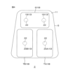
- 2 is a schematic front view of the conductor of FIG. 1.
- FIG. 3 is a schematic rear view (first embodiment) of the conductor of FIG. 1.
- FIG. 4 is a schematic rear view (second form) of the conductor of FIG. 1.
- FIG. 5 is a schematic rear view (third embodiment) of the conductor of FIG. 1.
- FIG. 6 is a diagram showing a first modification of the electrode wiring pattern of FIG.
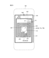
- FIG. 9 is a schematic front view of the device main body of FIG. 1.
- FIG. 10 is a schematic rear view of the device main body of FIG.
- FIG. 11 is a schematic plan view of the device main body of FIG. 1.
- FIG. 12 is a diagram showing a modification of the device main body of FIG.
- FIG. 13 is a diagram for explaining slits (first pattern) formed in the conductor.
- FIG. 14 is a diagram for explaining slits (second pattern) formed in the conductor.
- FIG. 15 is a diagram showing a modification of the arrangement direction of the slits in FIG.
- FIG. 16 is a diagram for explaining slits (third pattern) formed in the conductor.
- 17A and 17B are diagrams showing the state in which the slit is opened.
- FIG. 18 is a diagram showing thickness distribution (first pattern) in the conductive rubber layer.
- FIG. 19 is a cross-sectional view along line XIX-XIX in FIG. 18.
- FIG. 20 is a diagram showing thickness distribution (second pattern) in the conductive rubber layer.
- 21 is a cross-sectional view taken along line XXI-XXI of FIG. 20.
- FIG. 22 is a diagram showing a dense state of electrode wiring.
- FIG. 23 is a diagram showing a dense state of electrode wiring.
- FIG. 24 is a diagram for explaining the easy-to-separate processed portion of the sheet base material.
- FIG. 25 is a schematic perspective view of the mounting supporter.
- FIG. 26 is a schematic perspective view of the mounting supporter.
- 27A and 27B are diagrams showing states before and after deformation of the conductor pad portion.
- FIG. 28 is a diagram showing a state in which the conductor is attached using the attachment supporter.
- FIG. 29 is a diagram showing a state in which the conductor is attached using the attachment supporter.
- FIG. 30 is a diagram showing a state in which the conductor is attached using the attachment supporter.
- FIG. 1 is a perspective view showing the state of use of the electrical stimulator 1.
- FIG. 1 is a perspective view showing the state of use of the electrical stimulator 1.
- the electrical stimulation device 1 is, for example, a device (electrical stimulation treatment device).
- the electrical stimulator 1 will be mainly described as a device for treating dysuria, but the electrical stimulator 1 can treat not only dysuria but also urge fecal incontinence by electrical stimulation from the back side of the sacrum. , also contributes to the improvement of fecal incontinence, such as leaky fecal incontinence.
- the electrical stimulator 1 includes a conductor 2 for electrical stimulation, a device body 3, and a wiring cord 4.
- the electrode 2 includes a sheet base material 5, an indifferent electrode 6 and a pair of stimulation electrodes 7A, 7B. Since the conductor 2 is a sheet to which a plurality of electrodes are attached, it may be called an electrode pad, for example.
- Conductive sheets 8, 9A and 9B are attached to the indifferent electrode 6 and the pair of stimulating electrodes 7A and 7B, respectively.
- the conductive sheets 8, 9A, 9B may be prepared separately from the conductor 2 and attached at the time of use, or may be attached in advance to the electrodes 6, 7A, 7B as a standard form of the conductor 2 when shipped from the factory. may have been In the latter case, a protective film may be provided on the conductive sheets 8, 9A, 9B to prevent the conductive sheets 8, 9A, 9B from accidentally contacting and sticking to something.
- the conductive sheets 8, 9A, 9B are made of conductive adhesive gel, for example, in order to pass the current output from the pair of stimulating electrodes 7A, 7B to the human body 10.
- the conductive sheets 8, 9A, 9B are composed of pads having a thickness of about 0.8 mm.
- the conductive sheets 8, 9A, and 9B are translucent and have adhesiveness on both sides.
- the conductive sheets 8, 9A, and 9B are in the form of a translucent gel having adhesiveness, and may be called, for example, a conductive adhesive pad, a conductive gel pad, or the like.
- the electrode 2 is fixed to the skin of the human body 10 by attaching one surface of the conductive sheets 8, 9A, and 9B to the skin of the human body 10 (living body).
- an electrically conductive sheet 8 is attached to the indifferent electrode 6
- an electrically conductive sheet 9A is attached to one stimulation electrode 7A
- an electrically conductive sheet 9B is attached to the other stimulation electrode 7B.
- the device body 3 is electrically connected to the conductor 2 by a wiring cord 4 .
- the device body 3 incorporates a control circuit including, for example, a CPU, a memory such as a ROM and a RAM, and a timer.
- the patient can output an electric signal (voltage) for outputting a current of a predetermined frequency to the conductor 2 by operating various operation buttons 26 and the monitor 24 provided on the device main body 3. .
- electrical stimulation is applied to the human body 10 from the pair of stimulating electrodes 7A and 7B of the conductor 2.
- FIG. 2 is a schematic front view of the conductor 2 of FIG. 1.
- FIG. FIG. 3 is a schematic rear view (first form) of the conductor 2 of FIG.
- FIG. 4 is a schematic rear view (second form) of the conductor 2 of FIG.
- FIG. 5 is a schematic rear view (third form) of the conductor 2 of FIG.
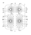
- 6 and 7 are diagrams respectively showing a first modification and a second modification of the pattern of the electrode wiring 21 of FIG.
- the electrode 2 includes a sheet base material 5, an indifferent electrode 6 and a pair of stimulation electrodes 7A, 7B.
- the sheet base material 5 is made of a flexible material that can be bent according to the bending (movable) of the human body 10 .
- the sheet base material 5 is a planar sheet member having insulating properties and having a first surface 11 pressed against the surface of the human body 10 and a second surface 12 opposite to the first surface 11.
- the shape of the sheet base material 5 is, in this embodiment, a rectangular shape with rounded corners (FIGS. 3 and 5 to 7) or a substantially triangular shape (FIG. 4), but is not particularly limited. It can be changed as appropriate according to the shape of the target site for electrical stimulation in 10 .
- the shape of the sheet base material 5 may be square, circular, or the like.
- the sheet base material 5 examples include insulating materials such as resin films, nonwoven fabrics, and paper. These may be used alone or in combination of two or more.
- the sheet substrate 5 is made of paper.
- paper examples include natural paper made from natural materials such as wood pulp and cotton pulp, synthetic paper made from synthetic resin materials such as synthetic resin pulp, and mixed materials of natural and synthetic resin materials. Any of the mixed papers used as raw materials may be used.
- the sheet base material 5 is made of paper, it is possible to provide the conductor 2 as a disposable item that is discarded after being used for a certain period of time.
- conductive sheets 8, 9A, and 9B conductive gel
- the adhesion of dirt, dust, etc. to the adhesive surface may increase the electrical resistance value of the conductive gel, making it difficult to output sufficient electrical stimulation to the human body. Therefore, it is preferable to replace the conductive gel periodically.
- the conductor 2 is a disposable item, the conductor 2 can be discarded together with the conductive gel without removing only the conductive gel when replacing the conductive gel. Therefore, when using the electrostimulator 1 on a daily basis, replacement work of the conductive gel is unnecessary. In particular, replacement work including alignment of the conductive gel is difficult for the elderly, so the burden during use is reduced.
- the thickness of the sheet base material 5 is not particularly limited as long as it has a strength that can withstand use as the electrode 2 for electrical stimulation, but may be, for example, 0.05 mm to 5 mm. .
- the second surface 12 of the sheet base material 5 is provided with a first terminal 19 and second terminals 20A and 20B as an example of a connecting portion.
- the first terminal 19 and the second terminals 20A, 20B are snap terminals 13 in this embodiment.
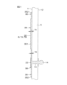
- the structure of the first terminal 19 will be specifically described with reference to FIG. Since the specific structure of the second terminals 20A and 20B is the same as that of the first terminal 19, detailed description thereof will be omitted.
- the snap terminals 13 are fixed so as to sandwich the sheet base material 5 and are exposed on both the first surface 11 and the second surface 12 of the sheet base material 5 .
- the snap terminal 13 is a male terminal in this embodiment and has a stud portion 14 projecting from the second surface 12 of the sheet substrate 5 .
- This stud portion 14 is used as a terminal portion for external connection, and is electrically connected to the electrical stimulator 1 via the wiring cord 4 .
- a snap terminal 16 (female terminal) covered with a cover 15 made of resin, for example, is provided at the tip of the wiring cord 4 .
- a recess 17 is formed in the snap terminal 16 .
- the snap terminal 16 is snap-coupled to the snap terminal 13 by fitting the stud portion 14 into the recess 17 .
- the number of snap terminals 13 is not particularly limited. In FIG. 2, as an example, two snap terminals 13 are provided on the side of the indifferent electrode 6, and one snap terminal 13 is provided on each side of the pair of stimulation electrodes 7A and 7B.
- the connection between the first terminal 19 and the second terminals 20A and 20B and the wiring cord 4 is not limited to the snap connection described above, and may be, for example, an insertion connection.
- an insertion type connector male type
- insertion openings thereof may be provided in the first terminal 19 and the second terminals 20A and 20B.
- the first terminal 19 and the second terminals 20A, 20B are formed of a conductive metal that attracts magnets, and the contact force between the first terminal 19 and the second terminals 20A, 20B is applied to the tip of the wiring cord 4 by magnetic force.
- a connector may be provided to maintain the
- An indifferent electrode 6 and a pair of stimulation electrodes 7A and 7B are formed on the first surface 11 of the sheet base material 5, respectively.
- first to third configurations of the indifferent electrode 6 and the pair of stimulating electrodes 7A, 7B will be described, respectively.
- the configurations of the indifferent electrode 6 and the pair of stimulation electrodes 7A and 7B are not limited to the structures shown in FIGS.
- the first form shown in FIG. 3 may be selectively applied only to the indifferent electrode 6, and the third form shown in FIGS. 5 to 7 may be applied to the pair of stimulation electrodes 7A and 7B.
- the indifferent electrode 6 and the pair of stimulation electrodes 7A and 7B may be formed of a conductive rubber layer 18 as an example of a conductive layer.
- the conductive rubber layer 18 is formed of a silicone rubber layer containing conductive carbon such as carbon black in this embodiment.
- the material of the conductive rubber layer 18 is not limited to silicone rubber containing carbon black, as long as it is a conductive rubber.
- the conductor (conductive filler) mixed in the silicone rubber may be carbon black, silver powder, gold-plated silica or graphite, conductive zinc oxide, or the like.
- ion conductive silicone rubber may be used as the material for the conductive rubber layer 18 .
- the conductive rubber layer 18 is formed in a planar shape covering a certain area of the first surface 11 of the sheet base material 5 .
- the “planar shape covering a certain area” is, for example, a shape that entirely covers a portion having a certain width on the first surface 11 of the sheet base material 5 .
- it can be defined as a square, a rectangle, a triangle, a circle, or the like, and may be a shape that is distinguished from line-shaped wiring.
- the conductive rubber layer 18 is formed in a rectangular shape to contact and cover the conduction point 22 of the snap terminal 13 exposed from the first surface 11 .
- the conductive rubber layer 18 is electrically connected to the snap terminals 13 via the conduction points 22 .
- the shape of the conductive rubber layer 18 is rectangular in this embodiment, it is not particularly limited and can be changed as appropriate according to the shape of the target region of the human body 10 for electrical stimulation.
- the shape of the conductive rubber layer 18 may be square, circular, triangular, or the like.
- the thickness of the conductive rubber layer 18 is not particularly limited, but may be, for example, 10 ⁇ m to 5000 ⁇ m.
- the conductive rubber layer 18 can be formed, for example, by coating a dispersion liquid in which conductive carbon is dispersed on the first surface 11 of the sheet base material 5 in a predetermined shape and solidifying the liquid.
- the electrode wiring 21 may be formed by a conductive wire having a predetermined width in this embodiment.
- Examples of the material of the electrode wiring 21 include silver, copper, etc.
- silver silver chloride (AgAgCl) wiring is used.
- the electrode wiring 21 is connected to the snap terminal 13 in a certain area of the first surface 11 of the sheet base material 5 at a connection point 22 (for example, a portion of the snap terminal 13 exposed from the first surface 11 of the sheet base material 5). It is stretched all around.
- the "certain region of the first surface 11" is a region to be brought into contact with the target site of electrical stimulation on the human body 10, for example, a region having a shape substantially matching the conductive sheets 8, 9A, 9B. good too. Therefore, the area where the electrode wiring 21 is formed may be defined as the gel placement area 30 .
- the gel placement region 30 is indicated by a phantom line consisting of two-dot chain lines.
- the electrode wiring 21 may be formed in a spiral pattern with one line surrounding the conduction point 22 starting from one point of the conduction point 22 .
- the electrode wiring 21 is formed by a plurality of mutually independent lines extending from a plurality of locations of the conduction points 22, and each line reciprocates in a serpentine pattern to form a gel. It may be spread all over the arrangement area 30 .
- the electrode wiring 21 may be formed in a radial pattern extending from a plurality of conductive points 22 as shown in FIG. By forming the electrode wirings 21 in this way, the electrode wirings 21 have a pattern in which they are arranged at intervals. Also, the electrode wiring 21 is electrically connected to the snap terminal 13 via the conduction point 22 .
- the width of the electrode wiring 21 is not particularly limited, it may be, for example, 0.5 mm to 10 mm.
- the thickness of the electrode wiring 21 is not particularly limited, but may be, for example, 10 ⁇ m to 5000 ⁇ m.
- the interval (pitch) of the electrode wiring 21 is not particularly limited, but may be, for example, 0.5 mm to 10 mm.
- the electrode wiring 21 is formed by, for example, printing a predetermined wiring pattern on the first surface 11 of the sheet base material 5 with a conductive ink containing a conductive substance (eg, silver-silver chloride ink, copper ink, etc.) and solidifying the ink. can be formed by [Configuration of the device body]
- FIG. 9 is a schematic front view of the device main body 3 of FIG. 1.
- FIG. 10 is a schematic rear view of the device main body 3 of FIG. 1.
- FIG. FIG. 11 is a schematic plan view of the device main body 3 of FIG. 1.
- FIG. 9 is a schematic front
- the device body 3 is a portable electrical stimulation therapy device.
- the device body 3 includes a housing 23 , a monitor 24 provided on the front surface of the housing 23 , and a start/stop button 25 and a plurality of operation buttons 26 provided below the monitor 24 .
- the housing 23 is formed in a substantially elliptical shape in this embodiment, and may be made of a plastic case, for example.
- a first insertion port 27 and a second insertion port 28 are provided on the upper surface of the housing 23 .
- the first receptacle 27 is, for example, an output port to which the wiring cord 4 is connected.
- the second receptacle 28 is, for example, a port for charging, and a cord of an AC adapter (not shown) is connected. That is, the device main body 3 can be turned on by power supplied from an outlet via a charged battery or an AC adapter.
- the monitor 24 may be formed in a long rectangular shape along the longitudinal direction of the housing 23 and arranged near one end in the longitudinal direction of the housing 23 . Also, the monitor 24 may be, for example, a monochrome or color liquid crystal monitor.
- the monitor 24 can display, for example, the pulse waveform and frequency of the electrical stimulation signal from the pair of stimulation electrodes 7A and 7B, the patient's electrocardiographic waveform and heart rate, messages to be notified to the patient, and the like. can. Thereby, the person to be treated can easily know the operating state of the electrical stimulation device 1 .
- the monitor 24 may be, for example, a touch panel on which a predetermined operation screen is displayed and the screen can be operated.
- the start/stop button 25 and the plurality of operation buttons 26 may be arranged on the other end side in the longitudinal direction of the housing 23 with respect to the monitor 24 .
- the operation button 26 may have various functions depending on the model of the electrical stimulation device 1 .
- a treatment menu including pulse wave widths (pulse widths) and frequencies of stimulation signals suitable for each of a plurality of subjects is stored in the device main body 3, and the treatment menus are stored in the device main body 3. It may be a button or the like that is operated when reading.
- the device main body 3 has a built-in reader 29 .
- the reader 29 may be built into the housing 23 on the other longitudinal end side of the housing 23 with respect to the monitor 24, or as shown in FIG. may be built into the
- the reader 29 may include, for example, a reader for reading RF tags used for RFID (Radio Frequency IDentifier).
- the device main body 3 may have a modified configuration shown in FIG. Referring to FIG. 12, device main body 3 is an installation type electrical stimulation therapy device.
- the device main body 3 is used in a state where it is always installed in a facility such as a hospital.
- the device main body 3 includes a housing 58, a monitor 59, a power button 60, an operation button 61, and a port 62 as a physical configuration.
- the housing 58 is formed in a substantially rectangular shape in this embodiment, and may be made of a plastic case, for example. Although not shown, the rear surface of the housing 58 may be provided with an insertion port for connecting an AC adapter or the like.
- the monitor 59 is provided on the front surface of the housing 58 .
- the monitor 59 may be formed in a long rectangular shape along the longitudinal direction of the housing 58 .
- Monitor 59 may be, for example, a monochrome or color liquid crystal monitor.
- the monitor 59 may be, for example, a touch panel on which a predetermined operation screen is displayed and the screen can be operated.
- the power button 60 and the operation button 61 are provided below the monitor 59, for example.
- the operation button 61 may have various functions depending on the model of the device body 3 .
- a treatment menu including pulse wave widths (pulse widths) and frequencies of stimulation signals suitable for each of a plurality of subjects is stored in the device main body 3 and read out. It may be a button or the like that is operated at the time.
- a plurality of ports 62 are provided on the front surface of the housing 58 .
- One conductor 2 is connected to each port 62 through the wiring cord 4 .
- the conductors 2 By connecting the conductors 2 to the ports 62 one by one, multiple patients can receive electrical stimulation therapy at the same time.
- the indifferent electrode and the stimulating electrode are formed in a flat sheet shape as a whole. Therefore, when the sheet is attached to the surface of a living body, a part of the electrode attachment surface may not be properly attached, and the sheet may be wrinkled. As a result, a space such as air bubbles is formed between the sheet and the surface of the living body, and electrical stimulation may not be efficiently transmitted to the surface of the living body. As a result, sufficient electrical stimulation cannot be output to the living body, and sufficient effects of electrical stimulation may not be obtained.
- slits 31, 32, and 33 are formed for three-dimensionally deforming the sheet base material 5. Variations in the pattern of the slits 31 to 33 will be described below with reference to FIGS. 13 to 16. FIG.
- FIG. 13 is a diagram for explaining the slits 31 (first pattern) formed in the conductor 2.
- FIG. FIG. 13 is a diagram corresponding to FIG. 3, in which the indifferent electrode 6 and the pair of stimulating electrodes 7A and 7B are formed of a conductive rubber layer 18.
- the width direction (horizontal direction) of the conductor 2 is defined as the first direction X
- the length direction (vertical direction) of the conductor 2 is defined as the second direction Y for convenience.
- a second direction Y is a direction orthogonal to the first direction X.
- the slit 31 is formed on almost the entire surface of the sheet base material 5.
- a plurality of slits 31 are formed in the sheet base material 5 .
- the slits 31 include linear first slits 311 extending in the first direction X and linear second slits 312 extending in the second direction Y.
- the first slits 311 and the second slits 312 are regularly arranged on the sheet base material 5 . More specifically, along the first direction X and the second direction Y, the first slits 311 and the second slits 312 are alternately arranged.
- the plurality of first slits 311 are arranged in a zigzag pattern so as not to be adjacent to each other in the first direction X and the second direction Y.
- the plurality of second slits 312 are arranged in a zigzag pattern so as not to be adjacent to each other in the first direction X and the second direction Y. As shown in FIG.
- Each first slit 311 and each second slit 312 have first ends 311A, 312A and opposite second ends 311B, 312B, respectively. Some of the first slits 311 and the second slits 312 may be formed so as to penetrate the sheet substrate 5 in regions where the conductive rubber layer 18 is not formed on the sheet substrate 5 . In addition, some other first slits 311 and second slits 312 are formed so as to overlap the conductive rubber layer 18 in the region where the conductive rubber layer 18 is formed in the sheet base material 5. good. Therefore, some first slits 311 and second slits 312 may continuously penetrate the conductive rubber layer 18 and the sheet base material 5 .
- At least one end 311A, 312A, 311B, 312B of each of the first slits 311 and each of the second slits 312 overlapping the conductive rubber layer 18 is arranged inside the outer peripheral edge 181 of the conductive rubber layer 18. .
- the conductive rubber layer 18 is not divided by the slits 31 . Therefore, electrical connection between the snap terminal 13 and the conductive rubber layer 18 can be secured over the entire conductive rubber layer 18 .
- FIG. 14 is a diagram for explaining the slits 32 (second pattern) formed in the conductor 2.
- FIG. FIG. 15 is a diagram showing a modification of the arrangement direction of the slits 32 in FIG. 14 and 15 are diagrams corresponding to FIG. 3, in which the indifferent electrode 6 and the pair of stimulation electrodes 7A and 7B are formed of a conductive rubber layer 18.
- FIG. 14 for convenience, the direction inclined by 45° with respect to the width direction (horizontal direction) of the conductor 2 is defined as the first direction X, and the direction orthogonal to the first direction X is defined as the second direction Y.
- the slit 32 is formed on almost the entire surface of the sheet base material 5.
- a plurality of slits 32 are formed in the sheet base material 5 .
- the slits 32 include linear first slits 321 extending in the first direction X and linear second slits 322 extending in the second direction Y.
- the first slits 321 and the second slits 322 are regularly arranged on the sheet base material 5 . More specifically, each of the plurality of slits 32 is formed as a cross slit by the first slit 321 and the second slit 322 crossing each other.
- a plurality of cross slits 32 are arranged in a matrix on the sheet base material 5 .
- the orientation of the plurality of cross slits 32 may be an X pattern as shown in FIG. 14 or a cross pattern as shown in FIG.
- Each first slit 321 and each second slit 322 have first ends 321A, 322A and opposite second ends 321B, 322B, respectively. Some of the first slits 321 and the second slits 322 may be formed to penetrate the sheet substrate 5 in regions where the conductive rubber layer 18 is not formed on the sheet substrate 5 . In addition, some other first slits 321 and second slits 322 are formed so as to overlap the conductive rubber layer 18 in the region where the conductive rubber layer 18 is formed in the sheet base material 5. good. Therefore, some first slits 321 and second slits 322 may continuously penetrate the conductive rubber layer 18 and the sheet base material 5 .
- At least one end 321A, 322A, 321B, 322B of each of the first slits 321 and each of the second slits 322 overlapping the conductive rubber layer 18 is arranged inside the outer peripheral edge 181 of the conductive rubber layer 18. .
- the conductive rubber layer 18 is not divided by the slits 32 . Therefore, electrical connection between the snap terminal 13 and the conductive rubber layer 18 can be secured over the entire conductive rubber layer 18 .
- FIG. 16 is a diagram for explaining the slits 33 (third pattern) formed in the conductor 2.
- FIG. 16 is a diagram corresponding to FIG. 5, in which the indifferent electrode 6 and the pair of stimulating electrodes 7A and 7B are formed by electrode wiring 21.
- the width direction (horizontal direction) of the conductor 2 is defined as the first direction X
- the length direction (vertical direction) of the conductor 2 is defined as the second direction Y for convenience.
- a second direction Y is a direction orthogonal to the first direction X.
- the number of turns of the electrode wiring 21 is reduced and the interval between the electrode wirings 21 is widened.
- a plurality of slits 33 are formed in the region 34 between the adjacent electrode wirings 21.
- the region 34 may include a first region 341 extending in the first direction X and a second region 342 extending in the second direction Y. good.
- the multiple slits 33 include first slits 331 formed in the first region 341 and second slits 332 formed in the second region 342 .
- the first slit 331 and the second slit 332 are formed along the electrode wiring 21 so as not to cross the electrode wiring 21 respectively.
- the first slit 331 and the second slit 332 are formed parallel to the electrode wiring 21 .
- the electrode wiring 21 is not divided by the slits 33 . Therefore, electrical connection between the snap terminal 13 and the electrode wiring 21 can be ensured over the entire electrode wiring 21 .
- the common items of the slits 31 to 33 is added.
- a plurality of slits 31 to 32 are preferably formed from the viewpoint of deforming the conductor 2 more flexibly.
- the number of slits 31-33 is not particularly limited.
- the dimension (length) of each of the slits 31 to 33 may be, for example, 0.25 cm to 10 cm.
- the interval between the adjacent slits 31 to 33 is, for example, 0.25 cm to 1.5 cm from the viewpoint of preventing the sheet base material 5 from tearing from the slits 31 to 33 and connecting the slits 31 to 33 with each other. is preferred.
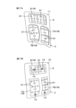
- FIG. 17A and 17B are diagrams showing the state in which the slit 31 is open. Next, the three-dimensional deformation of the conductor 2 by the slits 31 to 33 will be described with reference to the drawings relating to the slit 31.
- FIG. 17A and 17B are diagrams showing the state after the conductor 2 of FIG. 13 is deformed, but the number of slits 31 is reduced in order to clearly show the open state of the slits 31.
- the slits 31 to 33 are opened so that the sheet base material 5 can be three-dimensionally shaped according to the shape of the living body surface. can be transformed into Thereby, the electrode 2 can be well fitted to the surface of the living body.
- the sheet base material 5 can be flexibly deformed according to the shape of the living body surface.
- the slit 32 is a cross-shaped slit, it is possible to flexibly cope with deformation in all directions from the center of the cross-shaped slit 32 toward its periphery.
- the conductive sheets 8, 9A, 9B conductive gel
- the conductive sheets 8, 9A, 9B Air bubbles may occur between 9B and the conductive rubber layer 18 or electrode wiring 21 .
- air bubbles can be removed not only from the outer edges of the conductive sheets 8, 9A, and 9B, but also through the plurality of slits 31-33.
- the adhesion between the conductive sheets 8, 9A, and 9B and the conductive rubber layer 18 and the electrode wiring 21 can be improved (a large contact area can be secured). Electrical stimulation can be efficiently transmitted to the surface of the living body through the sheets 8, 9A, and 9B.
- regions are formed between the plurality of slits 31 to 33 to ensure electrical connection between the snap terminal 13 and the conductive rubber layer 18 (or between the snap terminal 13 and the electrode wiring 21).
- the entire conductive rubber layer 18 and electrode wiring 21 can be effectively used as a region for transmitting electrical stimulation to the surface of the living body.
- Electrode conductivity control For example, in the invention described in Patent Document 1, the indifferent electrode and the stimulating electrode are formed in a flat sheet shape as a whole. Therefore, the electrical resistance is uniform in the direction along the sheet surface, and voltage and current may be insufficient in areas where strong electrical stimulation is required, and excessive voltage and current may be supplied in areas where electrical stimulation is not so necessary. .
- the indifferent electrode 6 and the pair of stimulating electrodes 7A and 7B have different voltage and current magnitude distributions. Variations in voltage/current distribution of the indifferent electrode 6 and the pair of stimulation electrodes 7A and 7B will be described below with reference to FIGS. 18 to 23. FIG.
- FIG. 18 is a diagram showing the thickness distribution (first pattern) in the conductive rubber layer 18.
- FIG. 19 is a cross-sectional view along line XIX-XIX in FIG. 18.
- FIG. 18 and 19 selectively show the stimulation electrodes 7A shown in FIG. Since the thickness distribution of the conductive rubber layer 18 shown in FIG. 18 can be applied not only to the stimulating electrode 7A but also to the indifferent electrode 6 and the stimulating electrode 7B, in FIG. They are collectively defined as electrodes 35 .
- the conductive rubber layer 18 related to the electrode 35 in FIG. 18 includes a first portion 351 having a first thickness T1 and a second portion 352 having a second thickness T2 smaller than the first thickness T1.
- the relatively thick first portion 351 has a wider current path than the relatively thin second portion 352, resulting in a smaller resistance.
- the resistance value (first resistance value) of the first portion 351 may be 5 ⁇ to 10 ⁇
- the resistance value (second resistance value) of the second portion 352 may be 10 ⁇ to 50 ⁇ .
- the first thickness T1 may be, for example, 50 ⁇ m to 500 ⁇ m
- the second thickness T2 may be, for example, 10 ⁇ m to 50 ⁇ m.
- it may be continuously changed in the range of 5 ⁇ to 50 ⁇ and 10 ⁇ m to 500 ⁇ m between the first portion 351 and the second portion 352 .
- the conductive rubber layer 18 includes the first portion 351 and the second portion 352 having different resistance values, the voltage/current distribution is flexibly adjusted according to the biological site to which the conductor 2 is attached. be able to. For example, there is no need to separately form or embed a predetermined pattern of conductive material in the conductive rubber layer 18 in order to adjust the voltage/current distribution, so the structure of the conductor 2 can be simplified.
- the first portion 351 and the second portion 352 divide the coating amount of the coating liquid (in this embodiment, the dispersion liquid in which the conductive carbon is dispersed) when forming the conductive rubber layer 18 for each location. can be easily formed by
- the second portion 352 of the conductive rubber layer 18 is formed on the outer peripheral edge portion 36 of the conductive rubber layer 18, and the first portion 351 of the conductive rubber layer 18 is formed inside the outer peripheral edge portion 36. It is formed in the central region 37 .
- the outer peripheral edge portion 36 may be, for example, a portion extending inward from the outer peripheral edge 181 of the conductive rubber layer 18 (outline line of the conductive rubber layer 18) to 0.5 cm.
- the central region 37 may be the region surrounded by the outer peripheral edge 36 . Since the boundary between the first portion 351 and the second portion 352 is not straight like a line drawn with a ruler, in FIG. The area where the two parts 352 are formed is indicated by the white area around the hatching.
- the base material of the conductor 2 is the sheet base material 5 as in this embodiment, for example, when the conductor 2 is attached to the surface of the living body, a part of the outer peripheral edge portion 36 of the conductive rubber layer 18 is the surface of the living body. floating from the If electrical stimulation is applied to the living body surface from the electrode 2 in this state, a tingling pain may be felt in the vicinity of the outer peripheral edge 36 of the conductive rubber layer 18 . Therefore, according to the configuration of FIG. By increasing the resistance value of 36, it is possible to reduce the magnitude of the voltage/current at that portion. As a result, even if part of the outer peripheral edge portion 36 of the conductive rubber layer 18 is floating, it is possible to reduce discomfort such as prickling pain.
- FIG. 20 is a diagram showing the thickness distribution (second pattern) in the conductive rubber layer 18.
- FIG. 21 is a cross-sectional view taken along line XXI-XXI of FIG. 20.
- FIG. 20 and 21, as in FIG. 18, the indifferent electrode 6 and stimulating electrodes 7A and 7B are collectively defined as electrodes 35 for convenience. 18, 20, and 21 are denoted by the same reference numerals, and description thereof will be omitted.
- the second portion 352 of the conductive rubber layer 18 is formed in the terminal vicinity region 38 around the connection point 22 between the conductive rubber layer 18 and the snap terminal 13, and the first portion 352 of the conductive rubber layer 18 is formed. 351 is further around the second portion 352 and is formed in the terminal spacing region 39 away from the snap terminal 13 .
- the near-terminal region 38 may be, for example, a peripheral portion up to 5 cm from the snap terminal 13 .
- the terminal vicinity region 38 may be an outer peripheral portion around the snap terminal 13 and may be a region up to half of the width of the portion with the smallest width to the outer peripheral edge 181 of the conductive rubber layer 18 .
- the terminal separation region 39 may be a region from the terminal vicinity region 38 to the outer peripheral edge 181 of the conductive rubber layer 18 .
- the second portion 352 is also formed on the outer peripheral edge portion 36 of the conductive rubber layer 18, similarly to FIG.
- the entire conductive rubber layer 18 is Uniformity of voltage/current distribution can be achieved.
- FIG. 22 is a diagram showing a dense state of the electrode wirings 21.
- FIG. FIG. 22 selectively shows the stimulation electrodes 7A shown in FIG. 22 can be applied not only to the stimulating electrode 7A but also to the indifferent electrode 6 and the stimulating electrode 7B. Therefore, in FIG. Defined as electrode 40 .
- a dense pattern region 41 in which the electrode wirings 21 are arranged at a first interval W1 and a sparse pattern region 42 in which the electrode wirings 21 are arranged at a second interval W2 wider than the first interval W1. is formed.
- the dense pattern area 41 is an area where the electrode wirings 21 are denser than the sparse pattern area 42 .
- the number of electrode wirings 21 crossing the unit areas 43 having the same unit length is greater in the dense pattern area 41 than in the sparse pattern area 42 .
- the number of electrode wirings 21 crossing the unit area 43 of the sparse pattern area 42 is two, whereas the number of electrode wirings 21 crossing the unit area 43 of the dense pattern area 41 is six.
- the electrode wiring 21 includes a first portion 401 having a relatively low first resistance value and a second portion 402 having a second resistance value higher than the first resistance value.
- the resistance value (first resistance value) of the first portion 401 may be 5 ⁇ to 10 ⁇
- the resistance value (second resistance value) of the second portion 402 may be 10 ⁇ to 50 ⁇ .
- the first spacing W1 between the electrode wirings 21 in the dense pattern area 41 may be, for example, 0.5 mm to 5 mm
- the second spacing W2 between the electrode wirings 21 in the sparse pattern area 42 may be, for example, 5 mm to 10 mm.
- the distance between the first interval W1 of the dense pattern region 41 and the second interval W2 of the sparse pattern region 42 of the electrode wiring 21 may be changed continuously within a range of 0.5 mm to 10 mm.
- the second portion 402 of the electrode wiring 21 is formed in the outer peripheral edge portion 44 of the gel placement region 30, and the first portion 401 of the electrode wiring 21 is formed in the central region 45 inside the outer peripheral edge portion 44.
- the outer peripheral edge portion 44 may be, for example, a portion up to 0.5 cm inward from the outer peripheral edge 301 of the gel placement region 30 (the line where the outer peripheral edge of the conductive gel to be placed is supposed to be positioned).
- the central region 45 may be a region surrounded by the outer peripheral edge 44 .
- the second portion 402 having a relatively high second resistance value is arranged at the outer peripheral edge portion 44 of the gel placement region 30 , thereby increasing the resistance value of the outer peripheral edge portion 44 of the gel placement region 30 .
- the first portion 401 and the second portion 402 can be easily distinguished and formed by simply setting the printing pattern of the conductive ink when forming the electrode wiring 21 .
- FIG. 23 is a diagram showing another form of the dense state of the electrode wirings 21.
- FIG. FIG. 23 selectively shows the stimulation electrodes 7A shown in FIG. Since the dense state of the electrode wiring 21 shown in FIG. 23 can be applied not only to the stimulating electrode 7A but also to the indifferent electrode 6 and the stimulating electrode 7B, in FIG. Defined as electrode 40 .
- the electrode wiring 21 is spirally formed at a constant interval (pitch) P1.
- the electrode wiring 21 includes a dense pattern region 63 formed by wiring having a first width W1 and a sparse pattern region 64 formed by wiring having a second width W2 narrower than the first width W1. . Due to this width difference, the dense pattern region 63 is a region in which the electrode wirings 21 are denser than in the sparse pattern region 64 . For example, the area of the electrode wiring 21 crossing the unit areas 43 having the same unit length is larger in the dense pattern area 63 than in the sparse pattern area 64 .
- the electrode wiring 21 includes a first portion 403 having a relatively low first resistance value and a second portion 404 having a second resistance value higher than the first resistance value.
- the resistance value (first resistance value) of the first portion 403 may be 5 ⁇ to 10 ⁇
- the resistance value (second resistance value) of the second portion 404 may be 10 ⁇ to 50 ⁇ .
- the second portion 404 of the electrode wiring 21 is formed in the outer peripheral edge portion 44 of the gel placement region 30, and the first portion 403 of the electrode wiring 21 is formed in the central region 45 inside the outer peripheral edge portion 44.
- the outer peripheral edge portion 44 may be, for example, a portion up to 0.5 cm inward from the outer peripheral edge 301 of the gel placement region 30 (the line where the outer peripheral edge of the conductive gel to be placed is supposed to be positioned).
- the central region 45 may be a region surrounded by the outer peripheral edge 44 .
- the second portion 404 having a relatively high second resistance value is arranged on the outer peripheral edge portion 44 of the gel placement region 30 , thereby increasing the resistance value of the outer peripheral edge portion 44 of the gel placement region 30 .
- the first portion 403 and the second portion 404 can be easily distinguished and formed simply by setting the printing pattern of the conductive ink when forming the electrode wiring 21 .
- a sparse pattern region 64 is formed in the terminal vicinity region 38 and a dense pattern region 63 is formed in the terminal separation region 39 as shown in FIG. Uniformity of current distribution can be achieved.
- the conductor 2 is a disposable item having a sheet base material 5 made of paper
- the conductor 2 is discarded as it is after using the conductor for a certain period of time.
- the combustible sheet base material 5 formed of paper and the flame-retardant snap terminal 13 formed of metal are mixed in the conductor 2, the snap terminal 13 is removed and separated. There is a need.
- FIG. 24 is a diagram for explaining the easily separable portion 46 of the sheet base material 5.
- the easy-to-separate processed portion 46 is a portion formed by selectively processing a part of the sheet base material 5 and provides easy separation of the snap terminal 13 .
- the easily separable portion 46 is formed so as to surround the snap terminal 13 .
- the easily separable processed portion 46 surrounds substantially the entire circumference of the snap terminal 13 .
- the structure of the easily separable portion 46 is not particularly limited, but in this embodiment, it is a perforation line 47 formed so as to surround the snap terminal 13 .
- a knob 48 that can be raised from the sheet base material 5 may be formed on a part of the perforation line 47 in the circumferential direction. For example, by holding the knob 48 and pulling it forward, a portion of the sheet base material 5 surrounded by the perforation line 47 (between the terminal region 49 and its periphery) is torn with the perforation line 47 as a boundary. . Thereby, the snap terminal 13 is separated from the sheet substrate 5 together with the terminal area 49 . As a result, the sheet base material 5 made of paper and the snap terminal 13 made of metal can be easily separated, and can be separately discarded.
- the easy-to-separate processed portion 46 is not limited to the perforation line 47.
- a portion of the sheet base material 5 may be selectively thinned in a line shape (in FIG. 24, an annular ring surrounding the snap terminal 13). It may also be a formed tearable portion.
- [Configuration of mounting supporter] 25 is a schematic perspective view of the mounting supporter 50.
- FIG. FIG. 26 is a schematic perspective view of the mounting supporter 50.
- FIG. 27A and 27B are diagrams showing states before and after deformation of the conductor pad portion 51.
- FIG. 28 to 30 are diagrams showing a state in which the conductor is attached using the attachment supporter 50.
- FIG. 28 is a view of the human body 10 viewed from the front side
- FIG. 29 is a view of the human body 10 viewed from the back side
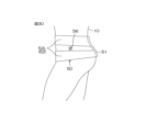
- FIG. 30 is a view of the human body 10 viewed from the left lateral side.
- the mounting supporter 50 is a device that assists the mounting of the electrode 2.
- the mounting supporter 50 includes a conductor pad portion 51 as an example of a conductor holding portion that holds the conductor 2 and a belt 52 connected to the conductor pad portion 51 .
- the mounting supporter 50 may integrally have a conductor pad portion 51 and a belt 52 formed of, for example, cloth.
- the conductor pad portion 51 and the belt 52 may be formed as separate parts and then connected to each other, for example, by sewing.
- the conductor pad portion 51 is provided in the center of the mounting supporter 50 .
- the conductor pad portion 51 is formed, for example, in a curved sheet shape recessed backward.
- the surface of the conductor pad portion 51 to which the second surface 12 of the sheet base material 5 is connected is a concave surface 53 .
- the planar shape of the conductor pad portion 51 is a substantially rectangular shape in accordance with the shape of the conductor 2, but may be other shapes such as a circular shape.
- a fixture 54 for fixing the conductor 2 to the conductor pad portion 51 is provided on the concave surface 53 .
- the fixture 54 is not particularly limited as long as it can fix the conductor 2, but it may be a snap button, for example.
- the belt 52 is stretchable in the left and right direction, and is connected to both the left and right sides of the conductor pad portion 51 .
- the belts 52 include a left belt 52L on the left side of the conductor pad portion 51 (right side in the drawing) and a right belt 52R on the right side of the conductor pad portion 51 (left side in the drawing).
- Each of the left belt 52L and the right belt 52R has two belts that are vertically spaced apart from each other.
- a fastener 55 for fixing the belts 52 to each other is provided at the tip of each belt 52 .
- the fastener 55 is not particularly limited as long as it can fix the belts 52 so that they do not separate from each other.
- FIG. 9B conductive gel
- the conductor 2 is fixed to the conductor pad portion 51 via the fixture 54 .
- the conductor 2 is held in a recessed shape along the concave surface 53 of the conductor pad portion 51 .
- a slit 31 see FIGS. 17A and 17B
- the slit 31 opens and the conductor 2 is three-dimensionally deformed, so that the conductor 2 is restrained from being stretched. It can be easily recessed along the concave surface 53 .
- the conductive sheets 8 , 9 A, and 9 B (conductive gel) can also be deformed into a recessed shape along the concave surface 53 . Therefore, as shown in FIG. 27A, until the conductor 2 is pressed against the surface of the human body 10, it is possible to prevent the conductive gel from inadvertently sticking to the surface of the body other than the target site for electrical stimulation, clothes, etc. can.
- the mounting supporter 50 is used to align the conductors 2 .
- the alignment is such that the conductor 2 rests on the back of the sacrum.
- a space 57 may be formed between the conductor 2 and the surface of the human body 10 .
- the belt 52 is pulled left and right and fixed with fasteners 55 as shown in FIG.
- FIG. 27B when the belt 52 is pulled left and right, the conductor pad portion 51 (curved sheet shape) is deformed so as to protrude forward in conjunction with the movement.
- the electrode 2 can be easily pressed against the surface of the human body 10. - ⁇ If the conductor 2 does not adhere to the surface of the human body 10 only by pulling the belt 52, the conductor pad portion 51 may be pushed from behind.
- the electrode 2 can be attached as shown in FIGS.
- two left belts 52L and two right belts 52R are provided with a vertical interval therebetween. Therefore, by fixing the mounting supporter 50 so as to sandwich the protrusion on the surface of the human body 10 such as the iliac crest 56 between the upper and lower belts 52, the positional deviation of the mounting supporter 50 can be suppressed.
- the base material is sheet-like
- the electrostimulation conductor when the electrostimulation conductor is attached to the surface of the living body, the base material follows the shape of the surface of the living body in the lateral direction (first surface and force is applied in the direction along the second surface).
- the slit is formed in the base material, the sheet-like base material can be three-dimensionally deformed according to the shape of the living body surface by opening the slit.
- the electrical stimulation conductor can be well fitted to the surface of the living body.
- air bubbles may be generated between the conductive gel and the conductive portion.
- air bubbles can be removed not only from the outer edge of the conductive gel but also through a plurality of slits.
- the adhesion between the conductive gel and the conductive portion can be improved (a large contact area can be secured), so that electrical stimulation can be efficiently transmitted from the conductive portion to the biological surface via the conductive gel.
- regions are formed between the plurality of slits to ensure electrical connection between the connecting portion and the conductive portion.
- the entire conductive portion can be effectively used as a region for transmitting electrical stimulation to the living body surface.
- Appendix 1-2 The electrical stimulation conductor according to Appendix 1-1, wherein the plurality of slits includes a first slit extending in a first direction and a second slit extending in a direction intersecting the first direction.
- the base material can be flexibly deformed according to the shape of the living body surface.
- Appendix 1-3 The electrical stimulation conductor according to Appendix 1-2, wherein the plurality of slits includes a cross slit formed by crossing the first slit and the second slit.
- Appendix 1-4 The electrical stimulation conductor according to Appendix 1-2 or Appendix 1-3, wherein the plurality of slits are formed by alternately arranging the first slits and the second slits.
- the first slits and the second slits having different opening directions can be evenly arranged without being biased for each region of the substrate surface.
- the substrate can be flexibly deformed according to the shape of the biological surface.
- the conductive part includes a conductive layer formed in a planar shape covering a certain area of the first surface of the base material,
- the plurality of slits have at least one end inside the outer peripheral edge of the conductive layer, and are formed to continuously penetrate the conductive layer and the base material, Appendix 1-1 to Appendix 1- 5.
- the electrode for electrical stimulation according to any one of 4.
- the base material and the conductive layer can be three-dimensionally deformed according to the shape of the living body surface by opening the slits. can. Moreover, since at least one end of the slit is located inside the outer peripheral edge of the conductive layer, the conductive layer is not divided by the slit. Thereby, the electrical connection between the connecting portion and the conductive layer can be secured over the entire conductive layer. Furthermore, since the conductive layer is formed in a planar shape, electrical stimulation can be efficiently transmitted to the living body surface from the entire region of the substrate where the conductive layer is formed.
- the conductive portion is an electrode wiring that is stretched around a point of conduction with the connection portion within a certain region of the first surface of the base material, and has patterns that are arranged at intervals.
- the electrical stimulation lead according to any one of Appendices 1-1 to 1-5, wherein the plurality of slits are formed along the electrode wiring in a region between the adjacent electrode wirings.
- the slit is formed in the region between the electrode wirings in the base material, a constant distance can be secured between the slits and the electrode wirings. Thereby, the insulation between the electrode wiring and the second surface side of the base material can be satisfactorily ensured. Also, since the slits are formed along the electrode wiring, the electrode wiring is not divided by the slits. Thereby, electrical connection between the connecting portion and the electrode wiring can be ensured over the entire electrode wiring.
- Appendix 1-7 The electrical stimulation conductor according to appendix 1-6, wherein the electrode wiring is spirally formed starting from the conduction point.
- the electrode for electrical stimulation as a disposable product, and since the discarded base material includes synthetic paper, it is possible to reduce the burden on the environment.
- a substrate formed of a sheet-like insulating material having a first surface to be pressed against the biological surface and a second surface on the opposite side; a conductive portion formed of a conductive material on the first surface of the base; a connecting portion formed on the second surface of the base material and conducting to the conductive portion;
- the conductive portion includes a first portion having a first resistance value, and a second portion having a second resistance value in a predetermined range selectively set higher than the first resistance value.
- the conductive portion includes the first portion and the second portion having different resistance values
- the voltage/current distribution can be flexibly adjusted according to the living body site to which the electrical stimulation conductor is attached. can be done. For example, it is not necessary to separately form or embed a predetermined pattern of conductive material in the conductive portion to adjust the voltage/current distribution, so the structure of the electrical stimulation conductor can be simplified.
- the conductive part includes a conductive layer formed in a planar shape covering a certain area of the first surface of the base material,
- the conductive layer includes the first portion having a first thickness and the second portion having a second thickness smaller than the first thickness,
- the electrical stimulation lead according to Appendix 1-9 is a conductive layer formed in a planar shape covering a certain area of the first surface of the base material,
- the conductive layer includes the first portion having a first thickness and the second portion having a second thickness smaller than the first thickness,
- the electrical stimulation lead according to Appendix 1-9 is a conductive layer formed in a planar shape covering a certain area of the first surface of the base material.
- the conductive portion is an electrode wiring that is stretched around a point of conduction with the connection portion within a certain region of the first surface of the base material, and has patterns that are arranged at intervals.
- the first surface of the base material includes a dense pattern region in which the electrode wirings are arranged at a first interval to form the first portion, and a dense pattern region in which the electrode wirings are arranged at a second interval wider than the first interval to form the first portion. and a sparsely patterned area forming two parts.
- the conductive portion is an electrode wiring that is stretched around a conductive point with the connection portion in a certain area of the first surface of the base material, and includes a pattern having electrode wiring with different widths,
- the first surface of the substrate includes a dense pattern area formed of the electrode wiring having a first width and a sparse pattern area formed of the electrode wiring having a second width narrower than the first width.
- the electrode for electrical stimulation according to appendix 1-9 comprising:
- the base material is sheet-like, for example, when the electrostimulation electrode is attached to the surface of the living body, part of the outer peripheral edge of the conductive part is in a state of floating from the surface of the living body. In this state, when electrical stimulation is applied from the electrode to the surface of the living body, a tingling pain may be felt in the vicinity of the outer peripheral edge of the conductive portion. Therefore, according to this configuration, by arranging the second portion having a relatively high second resistance value at the outer peripheral edge portion of the conductive portion, the resistance value of the outer peripheral edge portion of the conductive portion is increased to increase the resistance at the portion. voltage and current can be reduced. As a result, even if part of the outer peripheral edge of the conductive portion is floating, it is possible to reduce discomfort such as prickling pain.
- the second portion of the conductive portion is formed around a point of conduction with the connection portion in the conductive portion, and the first portion of the conductive portion is formed in a region further around the second portion.
- the electrode for electrical stimulation according to any one of Appendices 1-9 to 1-13.
- the voltage/current distribution is uniform. can be improved.
- Appendix 1-16 The electrical stimulation conductor according to any one of Appendixes 1-9 to 1-15, wherein the insulating material includes synthetic paper.
- the electrode for electrical stimulation as a disposable product, and since the discarded base material includes synthetic paper, it is possible to reduce the burden on the environment.
- the connecting portion includes a metal terminal fixed to the base material, Any one of Appendices 1-1 to 1-16, further comprising an easy-to-separate processed portion that is formed around the terminal in the base material and facilitates selective separation of a part of the base material together with the terminal.
- the metal terminals can be easily separated. Therefore, for example, when the electric stimulation conductor is a disposable product, the base material formed of the insulating material and the metal terminal can be easily separated and discarded.
- the cable of the electrical stimulation device that supplies electrical stimulation signals to the conductors can be easily connected to the connecting portion (snap terminal) by snap coupling, and can be easily removed.
- Appendix 1-20 The electrical stimulation conductor according to any one of Appendices 1-1 to 1-19, wherein the substrate comprises a paper substrate.
- the electrode for electrical stimulation as a disposable product, and since the discarded base material is made of paper, it is possible to reduce the burden on the environment.
- Appendix 1-21 a conductive gel formed to cover the conductive portion;
- the conductive gel is provided on the electrical stimulation conductor in advance, the work of attaching the conductive gel when using the conductor can be omitted. Moreover, since the conductive gel is covered with the protective film, it is possible to prevent the conductive gel from accidentally contacting and sticking to something.
- a conductor mounting supporter for assisting mounting of a sheet-like electrical stimulation conductor having a first surface to be pressed against a living body surface and a second surface on the opposite side thereof, Having a concave surface to which the second surface of the electrical stimulation conductor is connected along, and holding the electrical stimulation conductor in a recessed shape along the concave surface;
- a probe attachment supporter including a belt that is connected to the probe holding part and can be fixed to a living body.
- the electrical stimulation conductor can be held in a recessed shape along the concave surface.
- the conductive gel when the conductive gel is adhered to the conductive portion of the substrate and the conductor is used, the conductive gel can also be deformed into a recessed shape along the concave surface. Therefore, it is possible to prevent the conductive gel from inadvertently adhering to surfaces other than the electrical stimulation target site of the living body, clothes, etc., until the conductor is pressed against the surface of the living body.
- the electrode mounting supporter includes a supporter for mounting the electrode for electrical stimulation on the back of a person's waist
- the conductor holding portion includes a conductor pad portion formed in a curved sheet shape recessed backward
- the belt includes left and right belts connected to the left and right sides of the conductor pad portion,
- the conductor mounting supporter according to appendix 1-22 wherein when the belt is pulled left and right, the conductor pad section is deformed such that the curved sheet shape protrudes forward in conjunction with the movement of the belt.
- the electrode for electrical stimulation can be easily pressed against the surface of the living body.
- each of the left and right belts includes a plurality of belts that are vertically spaced apart from each other.
- the supporter can be restrained from being displaced by fixing the supporter so as to sandwich the protrusion of the living body surface such as the iliac crest between the upper and lower belts.
- Electrode 1 Electrical stimulation device 2: Electrode 3: Device main body 4: Wiring cord 5: Sheet base material 6: Indifferent electrode 7A: Stimulation electrode 7B: Stimulation electrode 8: Conductive sheet 9A: Conductive sheet 9B: Conductive sheet 10: Human body 11: First surface 12: Second surface 13: Snap terminal 14: Stud portion 15: Cover 16: Snap terminal 17: Recess 18: Conductive rubber layer 19: First terminal 20A: Second terminal 20B: Second terminal 2 terminals 21 : electrode wiring 22 : conduction point 23 : housing 24 : monitor 25 : stop button 26 : operation button 27 : first insertion port 28 : second insertion port 29 : reader 30 : gel placement area 31 : Slit 32 : Cross slit 33 : Slit 34 : Area 35 : Electrode 36 : Peripheral edge 37 : Central area 38 : Terminal vicinity area 39 : Terminal isolated area 40 : Electrode 41 : Dense pattern area 42 : Sparse pattern area 43 : Unit area 44 : Peripheral edge
Landscapes
- Health & Medical Sciences (AREA)
- Engineering & Computer Science (AREA)
- Biomedical Technology (AREA)
- Nuclear Medicine, Radiotherapy & Molecular Imaging (AREA)
- Radiology & Medical Imaging (AREA)
- Life Sciences & Earth Sciences (AREA)
- Animal Behavior & Ethology (AREA)
- General Health & Medical Sciences (AREA)
- Public Health (AREA)
- Veterinary Medicine (AREA)
- Electrotherapy Devices (AREA)
Priority Applications (1)
| Application Number | Priority Date | Filing Date | Title |
|---|---|---|---|
| JP2023569555A JPWO2023120677A1 (https=) | 2021-12-24 | 2022-12-22 |
Applications Claiming Priority (2)
| Application Number | Priority Date | Filing Date | Title |
|---|---|---|---|
| JP2021211364 | 2021-12-24 | ||
| JP2021-211364 | 2021-12-24 |
Publications (1)
| Publication Number | Publication Date |
|---|---|
| WO2023120677A1 true WO2023120677A1 (ja) | 2023-06-29 |
Family
ID=86902765
Family Applications (1)
| Application Number | Title | Priority Date | Filing Date |
|---|---|---|---|
| PCT/JP2022/047489 Ceased WO2023120677A1 (ja) | 2021-12-24 | 2022-12-22 | 電気刺激用導子および導子装着サポータ |
Country Status (2)
| Country | Link |
|---|---|
| JP (1) | JPWO2023120677A1 (https=) |
| WO (1) | WO2023120677A1 (https=) |
Citations (4)
| Publication number | Priority date | Publication date | Assignee | Title |
|---|---|---|---|---|
| JPH0719340U (ja) * | 1992-12-14 | 1995-04-07 | バンドー化学株式会社 | 皮膚貼付薬シ−ト |
| WO2005103186A1 (ja) * | 2004-04-22 | 2005-11-03 | Sekisui Plastics Co., Ltd. | ゲル粘着組成物 |
| JP2008264088A (ja) * | 2007-04-17 | 2008-11-06 | Ya Man Ltd | 電極パッド |
| JP2015000872A (ja) * | 2013-06-18 | 2015-01-05 | 日本電子精機株式会社 | 身体の曲面部及び/又は凹凸部を被覆する貼付剤 |
-
2022
- 2022-12-22 WO PCT/JP2022/047489 patent/WO2023120677A1/ja not_active Ceased
- 2022-12-22 JP JP2023569555A patent/JPWO2023120677A1/ja active Pending
Patent Citations (4)
| Publication number | Priority date | Publication date | Assignee | Title |
|---|---|---|---|---|
| JPH0719340U (ja) * | 1992-12-14 | 1995-04-07 | バンドー化学株式会社 | 皮膚貼付薬シ−ト |
| WO2005103186A1 (ja) * | 2004-04-22 | 2005-11-03 | Sekisui Plastics Co., Ltd. | ゲル粘着組成物 |
| JP2008264088A (ja) * | 2007-04-17 | 2008-11-06 | Ya Man Ltd | 電極パッド |
| JP2015000872A (ja) * | 2013-06-18 | 2015-01-05 | 日本電子精機株式会社 | 身体の曲面部及び/又は凹凸部を被覆する貼付剤 |
Also Published As
| Publication number | Publication date |
|---|---|
| JPWO2023120677A1 (https=) | 2023-06-29 |
Similar Documents
| Publication | Publication Date | Title |
|---|---|---|
| JP5667205B2 (ja) | 電流を身体組織に送るシステム | |
| US9757554B2 (en) | System for transmitting electrical current to a bodily tissue | |
| EP2588187B1 (en) | Disposable electrode for electro-stimulation | |
| US4736752A (en) | Transcutaneous medical electrode | |
| US4381789A (en) | Electrode system | |
| KR102494424B1 (ko) | 근육 전기 자극 장치 | |
| KR20180120556A (ko) | 근육 전기 자극 장치 | |
| EP2575955A1 (en) | Electrode assembly with magnetic connection | |
| WO1982000951A1 (en) | Automatic electrode placement device | |
| US4265253A (en) | Skin conducting electrode and electrode assembly | |
| JP2012024405A (ja) | 電気刺激治療用導子、および電気刺激治療装置 | |
| US5843155A (en) | Current-controlling electrode system | |
| EP2814562B1 (en) | Dual-sided current controlling electrode | |
| US11517751B2 (en) | Electrode for electrical stimulation therapy and electrical stimulation therapeutic device | |
| WO2023120677A1 (ja) | 電気刺激用導子および導子装着サポータ | |
| US20250128054A1 (en) | An electrode pad for electro-stimulation and method of manufacturing same | |
| CN116832321A (zh) | 治疗仪 | |
| GB2519743B (en) | Microcurrent electrical neuromuscular stimulator apparatus | |
| JP3266741B2 (ja) | 低周波治療器の電極導子及びその製造方法 | |
| CN224166724U (zh) | 一种多功能电疗仪 | |
| JP2617929B2 (ja) | 生体用電極 | |
| CN219557636U (zh) | 动物实验用电极片、动物实验组件及动物实验装置 | |
| CN221601059U (zh) | 电刺激膏贴理疗器 | |
| CN217567139U (zh) | 一种迷走神经刺激器 | |
| CN208770674U (zh) | 充电式穴位电疗贴 |
Legal Events
| Date | Code | Title | Description |
|---|---|---|---|
| 121 | Ep: the epo has been informed by wipo that ep was designated in this application |
Ref document number: 22911379 Country of ref document: EP Kind code of ref document: A1 |
|
| ENP | Entry into the national phase |
Ref document number: 2023569555 Country of ref document: JP Kind code of ref document: A |
|
| NENP | Non-entry into the national phase |
Ref country code: DE |
|
| 122 | Ep: pct application non-entry in european phase |
Ref document number: 22911379 Country of ref document: EP Kind code of ref document: A1 |