WO2023120353A1 - 半導体装置 - Google Patents
半導体装置 Download PDFInfo
- Publication number
- WO2023120353A1 WO2023120353A1 PCT/JP2022/046162 JP2022046162W WO2023120353A1 WO 2023120353 A1 WO2023120353 A1 WO 2023120353A1 JP 2022046162 W JP2022046162 W JP 2022046162W WO 2023120353 A1 WO2023120353 A1 WO 2023120353A1
- Authority
- WO
- WIPO (PCT)
- Prior art keywords
- layer
- semiconductor device
- electrode
- gate
- conductive
- Prior art date
- Legal status (The legal status is an assumption and is not a legal conclusion. Google has not performed a legal analysis and makes no representation as to the accuracy of the status listed.)
- Ceased
Links
Images


Classifications
-
- H—ELECTRICITY
- H10—SEMICONDUCTOR DEVICES; ELECTRIC SOLID-STATE DEVICES NOT OTHERWISE PROVIDED FOR
- H10W—GENERIC PACKAGES, INTERCONNECTIONS, CONNECTORS OR OTHER CONSTRUCTIONAL DETAILS OF DEVICES COVERED BY CLASS H10
- H10W72/00—Interconnections or connectors in packages
- H10W72/851—Dispositions of multiple connectors or interconnections
-
- H—ELECTRICITY
- H10—SEMICONDUCTOR DEVICES; ELECTRIC SOLID-STATE DEVICES NOT OTHERWISE PROVIDED FOR
- H10D—INORGANIC ELECTRIC SEMICONDUCTOR DEVICES
- H10D12/00—Bipolar devices controlled by the field effect, e.g. insulated-gate bipolar transistors [IGBT]
-
- H—ELECTRICITY
- H10—SEMICONDUCTOR DEVICES; ELECTRIC SOLID-STATE DEVICES NOT OTHERWISE PROVIDED FOR
- H10D—INORGANIC ELECTRIC SEMICONDUCTOR DEVICES
- H10D30/00—Field-effect transistors [FET]
- H10D30/60—Insulated-gate field-effect transistors [IGFET]
-
- H—ELECTRICITY
- H10—SEMICONDUCTOR DEVICES; ELECTRIC SOLID-STATE DEVICES NOT OTHERWISE PROVIDED FOR
- H10W—GENERIC PACKAGES, INTERCONNECTIONS, CONNECTORS OR OTHER CONSTRUCTIONAL DETAILS OF DEVICES COVERED BY CLASS H10
- H10W40/00—Arrangements for thermal protection or thermal control
- H10W40/20—Arrangements for cooling
- H10W40/25—Arrangements for cooling characterised by their materials
- H10W40/255—Arrangements for cooling characterised by their materials having a laminate or multilayered structure, e.g. direct bond copper [DBC] ceramic substrates
-
- H—ELECTRICITY
- H10—SEMICONDUCTOR DEVICES; ELECTRIC SOLID-STATE DEVICES NOT OTHERWISE PROVIDED FOR
- H10W—GENERIC PACKAGES, INTERCONNECTIONS, CONNECTORS OR OTHER CONSTRUCTIONAL DETAILS OF DEVICES COVERED BY CLASS H10
- H10W40/00—Arrangements for thermal protection or thermal control
- H10W40/20—Arrangements for cooling
- H10W40/25—Arrangements for cooling characterised by their materials
- H10W40/258—Metallic materials
-
- H—ELECTRICITY
- H10—SEMICONDUCTOR DEVICES; ELECTRIC SOLID-STATE DEVICES NOT OTHERWISE PROVIDED FOR
- H10W—GENERIC PACKAGES, INTERCONNECTIONS, CONNECTORS OR OTHER CONSTRUCTIONAL DETAILS OF DEVICES COVERED BY CLASS H10
- H10W72/00—Interconnections or connectors in packages
- H10W72/071—Connecting or disconnecting
- H10W72/075—Connecting or disconnecting of bond wires
-
- H—ELECTRICITY
- H10—SEMICONDUCTOR DEVICES; ELECTRIC SOLID-STATE DEVICES NOT OTHERWISE PROVIDED FOR
- H10W—GENERIC PACKAGES, INTERCONNECTIONS, CONNECTORS OR OTHER CONSTRUCTIONAL DETAILS OF DEVICES COVERED BY CLASS H10
- H10W72/00—Interconnections or connectors in packages
- H10W72/30—Die-attach connectors
-
- H—ELECTRICITY
- H10—SEMICONDUCTOR DEVICES; ELECTRIC SOLID-STATE DEVICES NOT OTHERWISE PROVIDED FOR
- H10W—GENERIC PACKAGES, INTERCONNECTIONS, CONNECTORS OR OTHER CONSTRUCTIONAL DETAILS OF DEVICES COVERED BY CLASS H10
- H10W72/00—Interconnections or connectors in packages
- H10W72/50—Bond wires
-
- H—ELECTRICITY
- H10—SEMICONDUCTOR DEVICES; ELECTRIC SOLID-STATE DEVICES NOT OTHERWISE PROVIDED FOR
- H10W—GENERIC PACKAGES, INTERCONNECTIONS, CONNECTORS OR OTHER CONSTRUCTIONAL DETAILS OF DEVICES COVERED BY CLASS H10
- H10W72/00—Interconnections or connectors in packages
- H10W72/851—Dispositions of multiple connectors or interconnections
- H10W72/874—On different surfaces
- H10W72/884—Die-attach connectors and bond wires
-
- H—ELECTRICITY
- H10—SEMICONDUCTOR DEVICES; ELECTRIC SOLID-STATE DEVICES NOT OTHERWISE PROVIDED FOR
- H10W—GENERIC PACKAGES, INTERCONNECTIONS, CONNECTORS OR OTHER CONSTRUCTIONAL DETAILS OF DEVICES COVERED BY CLASS H10
- H10W90/00—Package configurations
- H10W90/701—Package configurations characterised by the relative positions of pads or connectors relative to package parts
- H10W90/731—Package configurations characterised by the relative positions of pads or connectors relative to package parts of die-attach connectors
- H10W90/736—Package configurations characterised by the relative positions of pads or connectors relative to package parts of die-attach connectors between a chip and a stacked lead frame, conducting package substrate or heat sink
-
- H—ELECTRICITY
- H10—SEMICONDUCTOR DEVICES; ELECTRIC SOLID-STATE DEVICES NOT OTHERWISE PROVIDED FOR
- H10W—GENERIC PACKAGES, INTERCONNECTIONS, CONNECTORS OR OTHER CONSTRUCTIONAL DETAILS OF DEVICES COVERED BY CLASS H10
- H10W90/00—Package configurations
- H10W90/701—Package configurations characterised by the relative positions of pads or connectors relative to package parts
- H10W90/751—Package configurations characterised by the relative positions of pads or connectors relative to package parts of bond wires
- H10W90/756—Package configurations characterised by the relative positions of pads or connectors relative to package parts of bond wires between a chip and a stacked lead frame, conducting package substrate or heat sink
Definitions
- the present disclosure relates to semiconductor devices.
- Patent Document 1 discloses an example of the semiconductor device.
- a semiconductor device disclosed in Patent Document 1 includes a semiconductor element having a main surface electrode corresponding to a source electrode.
- the principal-surface electrode has a first portion and a plurality of second portions formed in a bump shape with respect to the first portion.
- a copper wire (a wire containing copper in its composition) is conductively joined to each of the plurality of second parts. Compared to gold wires, copper wires have a greater impact on the semiconductor elements to which they are electrically connected.
- the plurality of second parts function as relieving layers that reduce the impact on the semiconductor element.
- the relaxation layer is provided in an electrode of a semiconductor element having a switching function (a source electrode if the semiconductor element is a MOSFET) as in the semiconductor device disclosed in Patent Document 1, the relaxation layer is formed in the electrode by solid-phase diffusion. There is a measure to conduct conductive bonding to Thereby, the thermal resistance and the electrical resistance at the interface between the electrode and the relaxation layer can be reduced.
- the relaxation layer is conductively joined to the electrode by solid-phase diffusion, the relaxation layer may interfere with the gate finger depending on the structure of the semiconductor device. This can occur because the gate fingers include portions that protrude further into the relaxed layer than the electrodes of the semiconductor device. In this case, since the relaxation layer is subjected to pressure due to solid-phase diffusion, a large impact is transmitted from the relaxation layer to the semiconductor element through the gate fingers, and there is a possibility that the semiconductor element cracks.
- An object of the present disclosure is to provide a semiconductor device that is improved over conventional semiconductor devices.
- the present disclosure provides a semiconductor device capable of reducing the impact on a semiconductor element when conductively bonding a relaxation layer to an electrode of a semiconductor element having gate fingers by solid-phase diffusion.
- a semiconductor device provided by one aspect of the present disclosure includes a support member, a semiconductor element, a buffer layer, and a conductive member.
- the semiconductor element has a first electrode and a gate electrode located on the side opposite to the side facing the support member in the first direction, and is joined to the support member.
- the buffer layer is conductively joined to the first electrode.
- the conductive member is conductively joined to the buffer layer.
- a first solid phase diffusion bonding layer is positioned between the first electrode and the buffer layer.
- the semiconductor element has a gate finger located on the same side as the gate electrode in the first direction and connected to the gate electrode.
- the gate finger includes a protrusion that protrudes toward the buffer layer from the first electrode.
- the buffer layer has a recess that is recessed from the side facing the semiconductor element in the first direction. At least part of the protrusion is accommodated in the recess.
- the semiconductor device it is possible to reduce the impact on the semiconductor element when conductively bonding the relaxation layer to the electrode of the semiconductor element having gate fingers by solid-phase diffusion.
- FIG. 1 is a plan view of a semiconductor device according to a first embodiment of the present disclosure
- FIG. FIG. 2 is a plan view corresponding to FIG. 1, showing the encapsulating resin through.
- FIG. 3 is a plan view corresponding to FIG. 2, showing the first terminals in a see-through manner and omitting the illustration of the plurality of second conductive members.
- 4 is a bottom view of the semiconductor device shown in FIG. 1.
- FIG. 5 is a front view of the semiconductor device shown in FIG. 1.
- FIG. 6 is a left side view of the semiconductor device shown in FIG. 1.
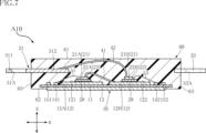
- FIG. FIG. 7 is a cross-sectional view along line VII-VII of FIG.
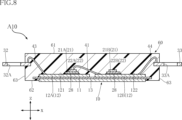
- FIG. 8 is a cross-sectional view along line VIII-VIII of FIG.
- FIG. 9 is a cross-sectional view along line IX-IX in FIG. 2.
- FIG. 10 is a partially enlarged view of FIG. 2.
- FIG. 11 is a cross-sectional view taken along line XI--XI in FIG. 10.
- FIG. 12 is a cross-sectional view taken along line XII-XII in FIG. 10.
- FIG. 13 is a partially enlarged view of FIG. 12.
- FIG. 14 is a partially enlarged view of FIG. 11.
- FIG. FIG. 15 is a partially enlarged cross-sectional view of a semiconductor device according to a second embodiment of the present disclosure; 16 is a partially enlarged cross-sectional view of the semiconductor device shown in FIG. 15, and the cross-sectional position is different from that of FIG. FIG.
- FIG. 17 is a partially enlarged cross-sectional view of a semiconductor device according to a third embodiment of the present disclosure
- 18 is a partially enlarged cross-sectional view of the semiconductor device shown in FIG. 17, and the cross-sectional position is different from that of FIG.
- FIG. 19 is a partially enlarged cross-sectional view of a semiconductor device according to a fourth embodiment of the present disclosure
- 20 is a partially enlarged view of FIG. 19.
- FIG. 1 A semiconductor device A10 according to the first embodiment of the present disclosure will be described based on FIGS. 1 to 14.
- FIG. The semiconductor device A10 includes a support member 10, a plurality of semiconductor elements 21, a plurality of buffer layers 22, a bonding layer 28, a first terminal 31, a second terminal 32, a third terminal 33, a plurality of first conduction members 41, a plurality of A second conduction member 42 , a third conduction member 43 , a fourth conduction member 44 and a sealing resin 60 are provided.
- the semiconductor device A10 includes a first gate wiring layer 141, a second gate wiring layer 142, a first detection wiring layer 151, a second detection wiring layer 152, a first gate terminal 341, a second gate terminal 342, and a first detection terminal. 351 and a second detection terminal 352 .
- FIG. 2 is transparent through the sealing resin 60 for convenience of understanding.
- FIG. 3 omits the illustration of the first terminals 31 and the plurality of second conductive members 42 as compared to FIG. 2 .
- the outline of the permeable sealing resin 60 is indicated by an imaginary line (chain double-dashed line).
- the transparent outline of the first terminal 31 is indicated by imaginary lines.
- the VII-VII line and the VIII-VIII line are indicated by one-dot chain lines.
- the normal direction of the first main surface 121 of the first conductive layer 12A which will be described later, will be referred to as the "first direction z".
- a direction orthogonal to the first direction z is called a “second direction x”.
- a direction perpendicular to both the first direction z and the second direction x is called a “third direction y”.
- the semiconductor device A 10 converts the DC power supply voltage applied to the first terminal 31 and the second terminal 32 into AC power by the plurality of semiconductor elements 21 .
- the converted AC power is input from the third terminal 33 to a power supply object such as a motor.
- the semiconductor device A10 forms part of a power conversion circuit such as an inverter.
- the support member 10 supports the first gate wiring layer 141 , the second gate wiring layer 142 , the first detection wiring layer 151 , the second detection wiring layer 152 and the sealing resin 60 while the plurality of semiconductor elements 21 are bonded to the support member 10 . are doing.
- the support member 10 includes an insulating layer 11, two conductive layers 12, and a heat dissipation layer 13. As shown in FIG.
- the insulating layer 11 includes two conductive layers 12, a first gate wiring layer 141, a second gate wiring layer 142, a first detection wiring layer 151, a second detection wiring layer 152, a heat dissipation layer 13 and a It supports the sealing resin 60 .
- the insulating layer 11 has electrical insulation.
- Insulating layer 11 is made of a material containing ceramics, for example. It is preferable that the ceramic has a higher thermal conductivity. An example of such ceramics is aluminum nitride (AlN).
- the material used for the insulating layer 11 preferably has a relatively high thermal conductivity.
- the insulating layer 11 has a peripheral edge 111 when viewed in the first direction z. The peripheral edge 111 forms the outline of the insulating layer 11 .
- the two conductive layers 12 are positioned between the insulating layer 11 and the plurality of semiconductor elements 21 in the first direction z, as shown in FIGS. Two conductive layers 12 are bonded to the insulating layer 11 . The two conductive layers 12 are surrounded by the peripheral edge 111 of the insulating layer 11 when viewed in the first direction z.
- the composition of the two conductive layers 12 includes copper (Cu). That is, each conductive layer 12 contains copper.
- the two conductive layers 12 include a first conductive layer 12A and a second conductive layer 12B spaced apart from each other in the second direction x.
- part of the first conductive layer 12A is cut into a rectangular shape with the long side in the third direction y.
- the notched portion of the first conductive layer 12A is located on the side opposite to the side facing the second conductive layer 12B in the second direction x.
- the first conductive layer 12A has a first major surface 121 .
- the first main surface 121 faces the side opposite to the side facing the insulating layer 11 in the first direction z.
- part of the second conductive layer 12B is cut into a rectangular shape with the long side in the third direction y.
- the notched portion of the second conductive layer 12B is located on the side opposite to the side facing the first conductive layer 12A in the second direction x.
- the second conductive layer 12B has a second major surface 122 .
- the second main surface 122 faces the side opposite to the side facing the insulating layer 11 in the first direction z.
- the heat dissipation layer 13 is located on the opposite side of the two conductive layers 12 with respect to the insulating layer 11 in the first direction z.
- the heat dissipation layer 13 is bonded to the insulating layer 11 .
- the heat dissipation layer 13 is surrounded by the peripheral edge 111 of the insulating layer 11 when viewed in the first direction z.
- the composition of the heat dissipation layer 13 contains copper.
- the area of the heat dissipation layer 13 is larger than the total area of the first conductive layer 12A and the second conductive layer 12B.
- the heat dissipation layer 13 is exposed outside from the sealing resin 60 .
- each of the two conductive layers 12 and the heat dissipation layer 13 is thicker than the thickness of the insulating layer 11 .
- a plurality of semiconductor elements 21 are bonded to two conductive layers 12, as shown in FIGS.
- the plurality of semiconductor elements 21 includes four first elements 21A and four second elements 21B.
- the four first elements 21A are bonded to the first main surface 121 of the first conductive layer 12A.
- the four second elements 21B are bonded to the second major surface 122 of the second conductive layer 12B.
- the plurality of semiconductor elements 21 are, for example, MOSFETs (Metal-Oxide-Semiconductor Field-Effect Transistors).
- the plurality of semiconductor elements 21 may be switching elements such as IGBTs (Insulated Gate Bipolar Transistors).
- the plurality of semiconductor elements 21 are n-channel MOSFETs with a vertical structure.
- the plurality of semiconductor elements 21 includes compound semiconductor substrates.
- the composition of the compound semiconductor substrate includes silicon carbide (SiC).
- SiC silicon carbide
- each of the semiconductor elements 21 has a first electrode 211 , a second electrode 212 , a gate electrode 213 and gate fingers 214 .
- the first electrode 211 is located on the side opposite to the side facing either of the two conductive layers 12 in the first direction z. A current corresponding to the power converted by the semiconductor element 21 flows through the first electrode 211 . That is, the first electrode 211 corresponds to the source electrode of the semiconductor element 21 .
- the second electrode 212 faces either of the two conductive layers 12. A current corresponding to the power before being converted by the semiconductor element 21 flows through the second electrode 212 . That is, the second electrode 212 corresponds to the drain electrode of the semiconductor element 21 .
- the gate electrode 213 is located on the side opposite to the side facing either of the two conductive layers 12 in the first direction z. Therefore, the gate electrode 213 is positioned on the same side as the first electrode 211 in the first direction z. A gate voltage for driving the semiconductor element 21 is applied to the gate electrode 213 .
- the area of the gate electrode 213 is smaller than the area of the first electrode 211 when viewed in the first direction z.
- the gate finger 214 is positioned on the same side as the gate electrode 213 in the first direction z.
- Gate finger 214 is connected to gate electrode 213 .
- the gate finger 214 extends from the gate electrode 213 in the second direction x.
- the gate finger 214 divides the first electrode 211 into two.
- the gate finger 214 electrically connects the gate electrode 213 and a plurality of trench gates formed inside the semiconductor element 21 (when the semiconductor element 21 is a trench gate type MOSFET).
- Gate fingers 214 include, for example, polysilicon and polyimide overlying the polysilicon. Gate finger 214 is thereby electrically isolated from the outside.
- the gate finger 214 includes a protrusion 214A.
- the convex portion 214A protrudes toward the buffer layer 22 from the first electrode 211 .
- the plurality of buffer layers 22 are individually conductively joined to the first electrodes 211 of the plurality of semiconductor elements 21, as shown in FIGS.
- the multiple buffer layers 22 include four first buffer layers 22A and four second buffer layers 22B.
- the four first buffer layers 22A are individually conductively joined to the first electrodes 211 of the four first elements 21A.
- the four second buffer layers 22B are individually conductively joined to the first electrodes 211 of the four second elements 21B.
- each of the multiple buffer layers 22 has a first layer 221 and a second layer 222 .
- the first layer 221 faces one of the first electrodes 211 of the plurality of semiconductor elements 21 in the first direction z.
- the composition of the first layer 221 contains aluminum (Al).
- the first layer 221 is formed by stacking a metal thin film on the second layer 222 by sputtering, for example.
- the second layer 222 is located on the opposite side of any one of the plurality of semiconductor elements 21 with respect to the first electrode 211 in the first direction z.
- the composition of the second layer 222 includes the same material (element) as the composition of the plurality of first conduction members 41 and the plurality of second conduction members 42 .
- the composition of the second layer 222 contains copper. Therefore, the Vickers hardness of the first layer 221 is lower than the Vickers hardness of the second layer 222 . Furthermore, the dimension t1 of the first layer 221 in the first direction z is smaller than the dimension t2 of the second layer 222 in the first direction z.
- the first layer 221 is conductively joined to any one of the first electrodes 211 of the plurality of semiconductor elements 21 by solid-phase diffusion. Therefore, as shown in FIG. 13 , a first solid-phase A diffusion bonding layer 291 is located. In the semiconductor device A10, the first solid phase diffusion bonding layer 291 is positioned between the first electrode 211 and the first layer 221. As shown in FIG. 13 , the first solid phase diffusion bonding layer 291 is positioned between the first electrode 211 and the first layer 221. As shown in FIG.
- the solid phase diffusion bonding layers are two solid phase diffusion bonding layers that are in contact with each other. It is the concept of a metal bonding layer located at the interface of the two metal layers as a result of the metal layers being bonded by solid state diffusion.
- a solid state diffusion bonding layer does not necessarily exist as a metallic bonding layer having a significant thickness.
- impurities and voids mixed in when bonding by solid-phase diffusion can sometimes be confirmed as portions remaining along the interface between the two metal layers.
- recesses 223 are formed in each of the multiple buffer layers 22 .
- the recess 223 is recessed from the side facing any one of the plurality of semiconductor elements 21 in the first direction z. At least part of the protrusion 214A of the gate finger 214 is accommodated in the recess 223. As shown in FIG.
- the protrusions 214A of the gate fingers 214 are located away from the buffer layer 22.
- the dimension h1 of the projection 214A in the first direction z is smaller than the dimension h2 of the recess 223 in the first direction z.
- the dimension t1 of the first layer 221 in the first direction z is larger than the dimension h2 of the recess 223 in the first direction z.
- the recess 223 has an intermediate surface 223A facing the protrusion 214A of the gate finger 214 in the first direction z.
- the intermediate surface 223A is recessed toward the inside of the first layer 221 .
- the intermediate surface 223A may be a plane parallel to either the first main surface 121 of the first conductive layer 12A or the second main surface 122 of the second conductive layer 12B.
- Recess 223 can be formed, for example, by laser irradiation.
- the bonding layer 28 is located between one of the two conductive layers 12 and the second electrode 212 of one of the plurality of semiconductor elements 21, as shown in FIG.
- the Vickers hardness of the bonding layer 28 is lower than the Vickers hardness of each of the two conductive layers 12 .
- the composition of the bonding layer 28 contains aluminum.
- the second electrodes 212 of the plurality of semiconductor elements 21 are electrically connected to one of the two conductive layers 12 via the bonding layer 28 . Thereby, the second electrodes 212 of the four first elements 21A are electrically connected to the first conductive layer 12A.
- the second electrodes 212 of the four second elements 21B are electrically connected to the second conductive layer 12B.
- the second electrode 212 of each of the plurality of semiconductor elements 21 is conductively bonded to one of the two conductive layers 12 via the bonding layer 28 by solid phase diffusion. Therefore, as shown in FIG. 14, a second solid-phase diffusion bonding layer 292 is located between one of the two conductive layers 12 and the bonding layer 28 .
- a third solid-phase diffusion bonding layer 293 is positioned between the bonding layer 28 and the second electrode 212 of one of the plurality of semiconductor elements 21 .
- the second solid phase diffusion bonding layer 292 and the third solid phase diffusion bonding layer 293 are formed at the same time as the first solid phase diffusion bonding layer 291 described above.
- the first gate wiring layer 141 is joined to the insulating layer 11 as shown in FIGS.
- the first gate wiring layer 141 is electrically connected to the gate electrodes 213 of the four first elements 21A.
- the first gate wiring layer 141 is located in the cutout portion of the first conductive layer 12A.
- the first gate wiring layer 141 extends along the third direction y.
- the composition of the first gate wiring layer 141 contains copper.
- Each of the plurality of first wires 51 is electrically connected to the gate electrode 213 of one of the four first elements 21A and the first gate wiring layer 141, as shown in FIG. As a result, the gate electrodes 213 of the four first elements 21 A are electrically connected to the first gate wiring layer 141 .
- the composition of the plurality of first wires 51 contains gold (Au). In addition, the composition of the plurality of first wires 51 may contain copper or aluminum.
- the first gate terminal 341 is located on one side of the third direction y with the support member 10 as a reference, as shown in FIGS.
- the first gate terminal 341 is electrically connected to the first gate wiring layer 141 .
- the first gate terminal 341 is a metal lead made of a material containing copper or copper alloy. As shown in FIGS. 1 and 9, part of the first gate terminal 341 is covered with the sealing resin 60 .
- the first gate terminal 341 is L-shaped when viewed in the second direction x. As shown in FIG. 5, the first gate terminal 341 includes a portion erected in the first direction z. The portion is exposed outside from the sealing resin 60 .
- a gate voltage for driving the four first elements 21A is applied to the first gate terminal 341 .
- the second gate wiring layer 142 is joined to the insulating layer 11, as shown in FIGS.
- the second gate wiring layer 142 is electrically connected to the gate electrodes 213 of the four second elements 21B.
- the second gate wiring layer 142 is located in the cutout portion of the second conductive layer 12B.
- the second gate wiring layer 142 extends along the third direction y.
- the composition of the second gate wiring layer 142 contains copper.
- Each of the plurality of third wires 53 is electrically connected to the gate electrode 213 of one of the four second elements 21B and the second gate wiring layer 142, as shown in FIG. Thereby, the gate electrodes 213 of the four second elements 21B are electrically connected to the second gate wiring layer 142 .
- the composition of the plurality of third wires 53 contains gold.
- the composition of the plurality of third wires 53 may contain copper or aluminum.
- the second gate terminal 342 is located on the same side as the first gate terminal 341 with respect to the support member 10 in the third direction y, as shown in FIGS.
- the second gate terminal 342 is electrically connected to the second gate wiring layer 142 .
- the second gate terminal 342 is a metal lead made of a material containing copper or copper alloy. As shown in FIG. 1 , part of the second gate terminal 342 is covered with the sealing resin 60 .
- the second gate terminal 342 is L-shaped when viewed in the second direction x. As shown in FIG. 5, the second gate terminal 342 includes a portion raised in the first direction z. The portion is exposed outside from the sealing resin 60 .
- a gate voltage for driving the four second elements 21B is applied to the second gate terminal 342 .
- the two fifth wires 55 are individually conductively bonded to the first gate terminal 341 and the second gate terminal 342 and the first gate wiring layer 141 and the second gate wiring layer 142, as shown in FIGS. It is Thereby, the first gate terminal 341 is electrically connected to the first gate wiring layer 141 .
- the second gate terminal 342 is electrically connected to the second gate wiring layer 142 .
- the composition of the two fifth wires 55 includes gold. Alternatively, the composition of the two fifth wires 55 may contain copper or aluminum.
- the first detection wiring layer 151 is joined to the insulating layer 11 as shown in FIGS.
- the first detection wiring layer 151 is electrically connected to the first electrodes 211 of the four first elements 21A.
- the first detection wiring layer 151 is positioned in the cutout portion of the first conductive layer 12A, and is positioned next to the first gate wiring layer 141 in the second direction x.
- the first detection wiring layer 151 extends along the third direction y.
- the composition of the first detection wiring layer 151 contains copper.
- Each of the plurality of second wires 52 is conductively joined to the first electrode 211 of one of the four first elements 21A and the first detection wiring layer 151, as shown in FIG. As a result, the first electrodes 211 of the four first elements 21A are electrically connected to the first detection wiring layer 151 .
- the composition of the plurality of second wires 52 includes gold. In addition, the composition of the second wire 52 may contain copper or aluminum.
- the first detection terminal 351 is located on the same side as the first gate terminal 341 with respect to the support member 10 in the third direction y, and is located on the same side as the first gate terminal 341 in the second direction x. located next to The first detection terminal 351 is electrically connected to the first detection wiring layer 151 .
- the first detection terminal 351 is a metal lead made of a material containing copper or copper alloy. As shown in FIG. 1 , part of the first detection terminal 351 is covered with the sealing resin 60 .
- the first detection terminal 351 is L-shaped when viewed in the second direction x. As shown in FIG. 5, the first detection terminal 351 includes a portion erected in the first direction z. The portion is exposed outside from the sealing resin 60 .
- a voltage having the same potential as the voltage applied to each of the first electrodes 211 of the four first elements 21A is applied to the first detection terminal 351 .
- the second detection wiring layer 152 is joined to the insulating layer 11 as shown in FIGS.
- the second detection wiring layer 152 is electrically connected to the first electrodes 211 of the four second elements 21B.
- the second detection wiring layer 152 is positioned in the cutout portion of the second conductive layer 12B, and is positioned next to the second gate wiring layer 142 in the second direction x.
- the second detection wiring layer 152 extends along the third direction y.
- the composition of the second detection wiring layer 152 contains copper.
- Each of the plurality of fourth wires 54 is conductively joined to the first electrode 211 of one of the four second elements 21B and the second detection wiring layer 152, as shown in FIG. As a result, the first electrodes 211 of the four second elements 21B are electrically connected to the first detection wiring layer 151 .
- the composition of the plurality of fourth wires 54 includes gold. In addition, the composition of the fourth wire 54 may contain copper or aluminum.
- the second detection terminal 352 is positioned on the same side as the second gate terminal 342 with respect to the support member 10 in the third direction y, and is positioned on the same side as the second gate terminal 342. and is located next to the second gate terminal 342 in the second direction x.
- the second detection terminal 352 is electrically connected to the second detection wiring layer 152 .
- the second detection terminal 352 is a metal lead made of a material containing copper or copper alloy. As shown in FIG. 1 , part of the second detection terminal 352 is covered with the sealing resin 60 .
- the second detection terminal 352 is L-shaped when viewed in the second direction x. As shown in FIG. 5, the second detection terminal 352 includes a portion erected in the first direction z. The portion is exposed outside from the sealing resin 60 .
- a voltage equal in potential to the voltage applied to each of the first electrodes 211 of the four second elements 21B is applied to the second detection terminal 352 .
- the two sixth wires 56 are individually conductively joined to the first detection terminal 351 and the second detection terminal 352 and the first detection wiring layer 151 and the second detection wiring layer 152, as shown in FIGS. It is Thereby, the first detection terminal 351 is electrically connected to the first detection wiring layer 151 .
- the second detection terminal 352 is electrically connected to the second detection wiring layer 152 .
- the composition of the two sixth wires 56 includes gold. Alternatively, the composition of the two sixth wires 56 may contain copper or aluminum.
- the first terminal 31 is located away from the first conductive layer 12A on the side facing the first main surface 121 of the first conductive layer 12A in the first direction z.
- the first terminal 31 is electrically connected to the first electrodes 211 of the four second elements 21B.
- the first terminal 31 is a metal plate made of a material containing copper or a copper alloy. As shown in FIG. 2, the first terminal 31 overlaps the first conductive layer 12A when viewed in the first direction z.
- the first terminal 31 has a terminal portion 311 and a base portion 312. As shown in FIG.
- the terminal portion 311 is positioned apart from the support member 10 when viewed in the first direction z.
- the terminal part 311 is positioned on one side of the second direction x with respect to the support member 10 .
- a portion of the terminal portion 311 is covered with the sealing resin 60 .
- the terminal portion 311 is provided with a first attachment hole 31A penetrating in the first direction z.
- the first attachment hole 31A is exposed outside from the sealing resin 60 .
- the terminal portion 311 is an N terminal (negative electrode) to which a DC power supply voltage to be converted is applied.
- the base portion 312 is connected to the terminal portion 311. As shown in FIG. The base 312 overlaps the insulating layer 11 , the first conductive layer 12 ⁇ /b>A, the first gate wiring layer 141 and the first detection wiring layer 151 when viewed in the first direction z.
- the base portion 312 is located on the opposite side of the second conductive layer 12B with respect to the four first elements 21A in the second direction x. When viewed in the first direction z, the base 312 has a rectangular shape with long sides in the third direction y.
- the base 312 is covered with the sealing resin 60 .
- the second terminal 32 is positioned apart from the first terminal 31 in the third direction y, as shown in FIGS.
- the second terminal 32 is positioned on the same side as the terminal portion 311 of the first terminal 31 with respect to the support member 10 in the second direction x.
- the second terminal 32 is electrically connected to the first conductive layer 12A.
- the second terminal 32 is a metal plate made of a material containing copper or copper alloy. A portion of the second terminal 32 is covered with the sealing resin 60 .
- the second terminal 32 is provided with a second attachment hole 32A penetrating in the first direction z. The second attachment hole 32A is exposed outside from the sealing resin 60 .
- the second terminal 32 is a P terminal (positive electrode) to which a DC power supply voltage to be converted is applied.
- the third conductive member 43 is joined to the second terminal 32 and the first main surface 121 of the first conductive layer 12A, as shown in FIGS. Thereby, the second terminal 32 is electrically connected to the first conductive layer 12A. Furthermore, in the semiconductor device A10, the second electrodes 212 of the four first elements 21A are electrically connected to the second terminals 32 via the first conductive layers 12A and the third conductive members 43. As shown in FIG. In the semiconductor device A10, the third conductive member 43 is a bonding wire.
- the composition of the third conduction member 43 contains either copper or aluminum. Alternatively, the third conducting member 43 may be a metal clip.
- the third terminal 33 is opposite to the terminal portion 311 of the first terminal 31 and the second terminal 32 with respect to the support member 10 in the second direction x. located on the side.
- the third terminal 33 is electrically connected to the second conductive layer 12B.
- the third terminal 33 is a metal plate made of a material containing copper or copper alloy. A portion of the third terminal 33 is covered with the sealing resin 60 .
- the third terminal 33 is provided with a third mounting hole 33A penetrating in the first direction z.
- the third attachment hole 33A is exposed outside from the sealing resin 60 .
- AC power converted by the plurality of semiconductor elements 21 is output from the third terminal 33 .
- the fourth conduction member 44 is joined to the third terminal 33 and the second main surface 122 of the second conductive layer 12B, as shown in FIGS. Thereby, the third terminal 33 is electrically connected to the second conductive layer 12B. Furthermore, in the semiconductor device A10, the second electrodes 212 of the four second elements 21B are electrically connected to the third terminal 33 via the second conductive layer 12B and the fourth conductive member 44. As shown in FIG. In the semiconductor device A10, the fourth conducting member 44 is a bonding wire. The composition of the fourth conduction member 44 contains either copper or aluminum. Alternatively, the fourth conducting member 44 may be a metal clip.
- each of the plurality of first conducting members 41 is electrically connected to one of the four first buffer layers 22A and the second main surface 122 of the second conductive layer 12B. It is As shown in FIGS. 10 and 11, each of the plurality of first conductive members 41 is conductively joined to the second layer 222 of one of the four first buffer layers 22A. Thereby, the first electrodes 211 of the four first elements 21A are electrically connected to the second conductive layer 12B. When viewed in the first direction z, each of the plurality of first conductive members 41 extends along the second direction x. In the semiconductor device A10, the plurality of first conduction members 41 are bonding wires. The composition of the plurality of first conduction members 41 contains copper.
- Each of the plurality of second conductive members 42 is joined to one of the four second buffer layers 22B and the first terminal 31, as shown in FIGS.
- each of the plurality of second conduction members 42 is joined to the base portion 312 of the first terminal 31 .
- each of the plurality of second conductive members 42 is conductively joined to the second layer 222 of any one of the four second buffer layers 22B.
- the first electrodes 211 of the four second elements 21B are electrically connected to the first terminals 31 .
- each of the plurality of second conductive members 42 overlaps the first conductive layer 12A.
- each of the plurality of second conduction members 42 when viewed in the first direction z, each of the plurality of second conduction members 42 extends along the second direction x and is connected to any of the four first elements 21A and the plurality of first conduction members 42A. It overlaps with any of the members 41 .
- the plurality of second conductive members 42 are bonding wires.
- the composition of the plurality of second conduction members 42 contains copper.
- the sealing resin 60 includes an insulating layer 11, two conductive layers 12, a first gate wiring layer 141, a second gate wiring layer 142, and a first detection wiring layer 151. , the second detection wiring layer 152 , the plurality of semiconductor elements 21 , the plurality of buffer layers 22 , the plurality of first conduction members 41 , the plurality of second conduction members 42 , the third conduction member 43 and the fourth conduction member 44 .
- the sealing resin 60 is applied to the heat dissipation layer 13 , the first terminal 31 , the second terminal 32 , the third terminal 33 , the first gate terminal 341 , the second gate terminal 342 , the first detection terminal 351 and the second detection terminal 352 . covering part of each.
- the sealing resin 60 has electrical insulation. Sealing resin 60 is made of a material containing, for example, black epoxy resin.
- the sealing resin 60 has a top surface 61, a bottom surface 62 and two side surfaces 63.
- the top surface 61 faces the same side as the first main surface 121 of the first conductive layer 12A in the first direction z.
- the bottom surface 62 faces the side opposite to the top surface 61 in the first direction z.
- the heat dissipation layer 13 is exposed to the outside from the bottom surface 62 .
- a portion of the heat dissipation layer 13 protrudes from the bottom surface 62 in the first direction z.
- the two side surfaces 63 are separated from each other in the second direction x and are connected to the top surface 61 and the bottom surface 62 .
- the terminal portion 311 of the first terminal 31 and the second terminal 32 are exposed to the outside from one of the two side surfaces 63 .
- the third terminal 33 is exposed to the outside from the other side surface 63 of the two side surfaces 63 .
- the semiconductor device A 10 has a first electrode 211 and gate fingers 214 , a semiconductor element 21 bonded to the support member 10 , and a buffer layer 22 conductively bonded to the first electrode 211 .
- a first solid phase diffusion bonding layer 291 is positioned between the first electrode 211 and the buffer layer 22 .
- Gate finger 214 includes a protrusion 214A that protrudes toward buffer layer 22 from first electrode 211 .
- the buffer layer 22 is formed with a recess 223 recessed from the side facing the semiconductor element 21 in the first direction z. At least part of the convex portion 214A is accommodated in the concave portion 223 .
- the buffer layer 22 has a first layer 221 and a second layer 222 located on the opposite side of the semiconductor element 21 with respect to the first layer 221 in the first direction z.
- the Vickers hardness of the first layer 221 is lower than the Vickers hardness of the second layer 222 .
- the dimension t1 of the first layer 221 in the first direction z is smaller than the dimension t2 of the second layer 222 in the first direction z.
- the composition of first layer 221 includes aluminum and the composition of second layer 222 includes copper.
- the protrusions 214A of the gate fingers 214 are located away from the buffer layer 22.
- the recess 223 formed in the buffer layer 22 has an intermediate surface 223A facing the protrusion 214A of the gate finger 214 in the first direction z.
- the intermediate surface 223A is recessed toward the inside of the first layer 221 . With this configuration, the volume of the recess 223 can be reduced when the dimension h2 of the recess 223 in the first direction z is fixed.
- the first conductive member 41 and the second conductive member 42 contain copper in their composition. By adopting this configuration, a larger current can flow through each of the first conduction member 41 and the second conduction member 42 .
- the composition of the second layer 222 of the buffer layer 22 contains the same copper as the composition of the first conductive member 41 and the second conductive member 42, The joint strength of each of the two conduction members 42 can be improved.
- the first terminal 31 overlaps the first conductive layer 12A when viewed in the first direction z. With this configuration, mutual inductance is generated between the first conductive layer 12A and the first terminal 31, so that the parasitic inductance appearing in each of the first conductive layer 12A and the first terminal 31 can be reduced. Therefore, the surge voltage to be applied to the first element 21A can be reduced, and power loss in the first conductive layer 12A can be suppressed.
- the second conductive member 42 overlaps the first element 21A when viewed in the first direction z. This contributes to the reduction of the dimension in the third direction y of the semiconductor device A10. Furthermore, when viewed in the first direction z, the second conducting member 42 overlaps the first conducting member 41 .
- mutual inductance is generated in the first conduction member 41 and the second conduction member 42, so the parasitic inductance appearing in each of the first conduction member 41 and the second conduction member 42 can be reduced. Therefore, power loss in the first conducting member 41 can be further suppressed.
- the support member 10 includes a heat dissipation layer 13 located on the opposite side of the conductive layer 12 with respect to the insulating layer 11 in the first direction z.
- the heat dissipation layer 13 is exposed outside from the bottom surface 62 of the sealing resin 60 .
- the conductive layer 12 and the heat dissipation layer 13 are surrounded by the peripheral edge 111 of the insulating layer 11 when viewed in the first direction z.
- the dimension of the conductive layer 12 in the first direction z is larger than the dimension of the insulating layer 11 in the first direction z.
- FIG. 15 is the same as the cross-sectional position of FIG. 11 showing the semiconductor device A10.
- the cross-sectional position of FIG. 16 is the same as the cross-sectional position of FIG. 12 showing the semiconductor device A10.
- the configuration of the plurality of buffer layers 22 is different from that of the semiconductor device A10.
- the recesses 223 formed in each of the multiple buffer layers 22 penetrate the first layer 221 in the first direction z and recess into the second layer 222 . Therefore, in the semiconductor device A20, the dimension t1 of the first layer 221 in the first direction z is smaller than the dimension h2 of the recess 223 in the first direction z.
- the semiconductor device A20 has a first electrode 211 and gate fingers 214, a semiconductor element 21 bonded to the support member 10, and a buffer layer 22 conductively bonded to the first electrode 211.
- a first solid phase diffusion bonding layer 291 is positioned between the first electrode 211 and the buffer layer 22 .
- Gate finger 214 includes a protrusion 214A that protrudes toward buffer layer 22 from first electrode 211 .
- the buffer layer 22 is formed with a recess 223 recessed from the side facing the semiconductor element 21 in the first direction z. At least part of the convex portion 214A is accommodated in the concave portion 223 .
- the semiconductor device A20 can also reduce the impact on the semiconductor element 21 when the buffer layer 22 is conductively joined to the electrode (first electrode 211) of the semiconductor element 21 having the gate finger 214 by solid-phase diffusion. It becomes possible. Furthermore, since the semiconductor device A20 has the same configuration as the semiconductor device A10, the semiconductor device A20 also exhibits the effects of the configuration.
- the dimension t1 of the first layer 221 of the buffer layer 22 in the first direction z is smaller than the dimension h2 of the recess 223 formed in the buffer layer 22 in the first direction z.
- the dimension t1 of the first layer 221 in the first direction z can be reduced while improving the bonding state of the first solid-phase diffusion bonding layer 291 located between the first electrode 211 and the buffer layer 22.
- the dimension t2 of the second layer 222 in the first direction z can be set as small as possible and the dimension t2 in the first direction z can be set as large as possible.
- the thermal resistance of the buffer layer 22 in the first direction z is further reduced and Heat conducting in the orthogonal direction is further increased. Thereby, further improvement of the heat dissipation of the buffer layer 22 can be aimed at.
- FIG. 17 is the same as the cross-sectional position of FIG. 11 showing the semiconductor device A10.
- the cross-sectional position of FIG. 18 is the same as the cross-sectional position of FIG. 12 showing the semiconductor device A10.
- the configuration of the plurality of buffer layers 22 is different from that of the semiconductor device A10.
- the protrusions 214A of the gate fingers 214 of each of the plurality of semiconductor elements 21 are in contact with any first layer 221 of the plurality of buffer layers 22. As shown in FIGS. The Vickers hardness of the first layer 221 is lower than the Vickers hardness of the protrusion 214A.
- the semiconductor device A30 has a first electrode 211 and gate fingers 214, a semiconductor element 21 bonded to the support member 10, and a buffer layer 22 conductively bonded to the first electrode 211.
- a first solid phase diffusion bonding layer 291 is positioned between the first electrode 211 and the buffer layer 22 .
- Gate finger 214 includes a protrusion 214A that protrudes toward buffer layer 22 from first electrode 211 .
- the buffer layer 22 is formed with a recess 223 recessed from the side facing the semiconductor element 21 in the first direction z. At least part of the convex portion 214A is accommodated in the concave portion 223 .
- the semiconductor device A30 can also reduce the impact on the semiconductor element 21 when the buffer layer 22 is conductively joined to the electrode (first electrode 211) of the semiconductor element 21 having the gate finger 214 by solid-phase diffusion. It becomes possible. Further, since the semiconductor device A30 has the same configuration as the semiconductor device A10, the semiconductor device A30 also exhibits the effects of the configuration.
- the protrusion 214A of the gate finger 214 is in contact with the first layer 221 of the buffer layer 22.
- the Vickers hardness of the first layer 221 is lower than the Vickers hardness of the protrusion 214A.
- FIGS. 19 and 20 A semiconductor device A40 according to the fourth embodiment of the present disclosure will be described based on FIGS. 19 and 20.
- FIG. In these figures, elements identical or similar to those of the semiconductor device A10 described above are denoted by the same reference numerals, and overlapping descriptions are omitted.
- the cross-sectional position of FIG. 19 is the same as the cross-sectional position of FIG. 12 showing the semiconductor device A10.
- the semiconductor device A40 is different from the semiconductor device A10 in the structure of the plurality of buffer layers 22 and in that the intermediate layer 23 is further provided.
- each of the multiple buffer layers 22 has a third layer 224 .
- the third layer 224 is located on the side opposite to the second layer 222 with respect to the first layer 221 .
- the recess 223 penetrates the third layer 224 in the first direction z.
- the Vickers hardness of the third layer 224 is higher than the Vickers hardness of the first layer 221 and lower than the Vickers hardness of the second layer 222 .
- the composition of the third layer 224 includes silver (Ag).
- the third layer 224 is formed by laminating a metal thin film on the first layer 221 by sputtering, for example.
- the intermediate layer 23 is positioned between the first electrode 211 of one of the plurality of semiconductor elements 21 and the third layer 224 of one of the plurality of buffer layers 22, as shown in FIG.
- the Vickers hardness of the intermediate layer 23 is higher than the Vickers hardness of the first layer 221 and lower than the Vickers hardness of the second layer 222 .
- the composition of the intermediate layer 23 contains silver.
- Intermediate layer 23 is formed by, for example, depositing a metal layer on first electrode 211 by electroplating.
- the first solid-phase diffusion bonding layer 291 is positioned between the intermediate layer 23 and any third layer 224 of the plurality of buffer layers 22. As shown in FIG. 20, in the semiconductor device A40, the first solid-phase diffusion bonding layer 291 is positioned between the intermediate layer 23 and any third layer 224 of the plurality of buffer layers 22. As shown in FIG. 20, in the semiconductor device A40, the first solid-phase diffusion bonding layer 291 is positioned between the intermediate layer 23 and any third layer 224 of the plurality of buffer layers 22. As shown in FIG.
- the semiconductor device A40 has a first electrode 211 and gate fingers 214, and includes a semiconductor element 21 bonded to the support member 10 and a buffer layer 22 conductively bonded to the first electrode 211.
- a first solid phase diffusion bonding layer 291 is located between the first electrode 211 and the buffer layer 22 .
- Gate finger 214 includes a protrusion 214A that protrudes toward buffer layer 22 from first electrode 211 .
- the buffer layer 22 is formed with a recess 223 recessed from the side facing the semiconductor element 21 in the first direction z. At least part of the convex portion 214A is accommodated in the concave portion 223 .
- the semiconductor device A40 can also reduce the impact on the semiconductor element 21 when the buffer layer 22 is conductively joined to the electrode (first electrode 211) of the semiconductor element 21 having the gate fingers 214 by solid-phase diffusion. It becomes possible. Furthermore, since the semiconductor device A40 has the same configuration as the semiconductor device A10, the semiconductor device A40 also exhibits the effects of the configuration.
- the buffer layer 22 has a third layer 224 located on the side opposite to the second layer 222 with respect to the first layer 221.
- the semiconductor device A40 further includes an intermediate layer 23 located between the first electrode 211 of the semiconductor element 21 and the third layer 224 .
- the Vickers hardness of each of the third layer 224 and the intermediate layer 23 is higher than the Vickers hardness of the first layer 221 and lower than the Vickers hardness of the second layer 222 .
- the first solid phase diffusion bonding layer 291 is located between the intermediate layer 23 and the third layer 224 .
- Appendix 1 a support member; a semiconductor element having a first electrode and a gate electrode positioned opposite to the side facing the support member in a first direction and bonded to the support member; a buffer layer conductively bonded to the first electrode; a conductive member conductively joined to the buffer layer, A first solid phase diffusion bonding layer is positioned between the first electrode and the buffer layer, the semiconductor element has a gate finger positioned on the same side as the gate electrode in the first direction and connected to the gate electrode; the gate finger includes a protrusion that protrudes toward the buffer layer from the first electrode;
- the buffer layer is formed with a recess that is recessed from a side facing the semiconductor element in the first direction, A semiconductor device, wherein at least part of the protrusion is accommodated in the recess.
- the buffer layer has a first layer and a second layer located on the opposite side of the semiconductor element with respect to the first layer in the first direction,
- the conducting member is conductively joined to the second layer,
- the semiconductor device according to appendix 1 wherein the Vickers hardness of the first layer is lower than the Vickers hardness of the second layer.
- Appendix 3. The semiconductor device according to appendix 2, wherein the dimension of the first layer in the first direction is smaller than the dimension of the second layer in the first direction.
- Appendix 4. 4.
- Appendix 5. 5 The semiconductor device according to appendix 4, wherein the composition of each of the second layer and the conductive member includes copper.
- Appendix 6. The semiconductor device according to appendix 4 or 5, wherein the conductive member is a bonding wire.
- Appendix 7. The semiconductor device according to any one of Appendixes 4 to 6, wherein the composition of the first layer contains aluminum.
- Appendix 8. It also has an intermediate layer, The buffer layer has a third layer located on the side opposite to the second layer with respect to the first layer, The intermediate layer is located between the first electrode and the third layer, The semiconductor according to any one of Appendices 2 to 7, wherein each of the third layer and the intermediate layer has a Vickers hardness greater than the Vickers hardness of the first layer and less than the Vickers hardness of the second layer.
- the semiconductor device according to appendix 8 wherein the first solid phase diffusion bonding layer is located between the intermediate layer and the third layer.
- Appendix 10. The convex portion is in contact with the first layer, 10.
- Appendix 11. 10.
- the semiconductor device according to any one of Appendices 2 to 9, wherein the protrusion is located away from the buffer layer.
- Appendix 12. 12 The semiconductor device according to appendix 11, wherein the dimension of the first layer in the first direction is greater than the dimension of the recess in the first direction. Appendix 13. 12.
- the semiconductor device according to appendix 11, wherein the dimension of the first layer in the first direction is smaller than the dimension of the recess in the first direction.
- Appendix 14. the concave portion has an intermediate surface facing the convex portion in the first direction; 14.
- Appendix 15. the support member includes an insulating layer and a conductive layer positioned between the insulating layer and the semiconductor element;
- the semiconductor element has a second electrode facing the conductive layer in the first direction, 15.
- the semiconductor device according to any one of Appendixes 1 to 14, wherein the second electrode is conductively joined to the conductive layer.
- the semiconductor device according to appendix 15 further comprising a bonding layer positioned between the conductive layer and the semiconductor element; Vickers hardness of the bonding layer is lower than Vickers hardness of the conductive layer, A second solid phase diffusion bonding layer is positioned between the conductive layer and the bonding layer, 16.
- the support member includes a heat dissipation layer located on the opposite side of the conductive layer with respect to the insulating layer in the first direction, 17.
- the semiconductor device according to appendix 15 or 16 wherein the conductive layer and the heat dissipation layer are surrounded by a peripheral edge of the insulating layer when viewed in the first direction.
Landscapes
- Cooling Or The Like Of Semiconductors Or Solid State Devices (AREA)
- Chemical & Material Sciences (AREA)
- Engineering & Computer Science (AREA)
- Materials Engineering (AREA)
Priority Applications (4)
| Application Number | Priority Date | Filing Date | Title |
|---|---|---|---|
| DE112022005481.6T DE112022005481T5 (de) | 2021-12-21 | 2022-12-15 | Halbleiterbauteil |
| CN202280084122.6A CN118414711A (zh) | 2021-12-21 | 2022-12-15 | 半导体装置 |
| JP2023569362A JPWO2023120353A1 (https=) | 2021-12-21 | 2022-12-15 | |
| US18/667,009 US20240304589A1 (en) | 2021-12-21 | 2024-05-17 | Semiconductor device |
Applications Claiming Priority (2)
| Application Number | Priority Date | Filing Date | Title |
|---|---|---|---|
| JP2021207018 | 2021-12-21 | ||
| JP2021-207018 | 2021-12-21 |
Related Child Applications (1)
| Application Number | Title | Priority Date | Filing Date |
|---|---|---|---|
| US18/667,009 Continuation US20240304589A1 (en) | 2021-12-21 | 2024-05-17 | Semiconductor device |
Publications (1)
| Publication Number | Publication Date |
|---|---|
| WO2023120353A1 true WO2023120353A1 (ja) | 2023-06-29 |
Family
ID=86902511
Family Applications (1)
| Application Number | Title | Priority Date | Filing Date |
|---|---|---|---|
| PCT/JP2022/046162 Ceased WO2023120353A1 (ja) | 2021-12-21 | 2022-12-15 | 半導体装置 |
Country Status (5)
| Country | Link |
|---|---|
| US (1) | US20240304589A1 (https=) |
| JP (1) | JPWO2023120353A1 (https=) |
| CN (1) | CN118414711A (https=) |
| DE (1) | DE112022005481T5 (https=) |
| WO (1) | WO2023120353A1 (https=) |
Citations (4)
| Publication number | Priority date | Publication date | Assignee | Title |
|---|---|---|---|---|
| JP2021007182A (ja) * | 2020-10-19 | 2021-01-21 | 三菱電機株式会社 | 半導体装置及びその製造方法 |
| JP2021093425A (ja) * | 2019-12-09 | 2021-06-17 | 株式会社デンソー | 半導体モジュール |
| JP2021128962A (ja) * | 2020-02-10 | 2021-09-02 | トヨタ自動車株式会社 | 半導体モジュール |
| WO2021235020A1 (ja) * | 2020-05-20 | 2021-11-25 | 日立Astemo株式会社 | パワー半導体素子 |
-
2022
- 2022-12-15 WO PCT/JP2022/046162 patent/WO2023120353A1/ja not_active Ceased
- 2022-12-15 CN CN202280084122.6A patent/CN118414711A/zh active Pending
- 2022-12-15 JP JP2023569362A patent/JPWO2023120353A1/ja active Pending
- 2022-12-15 DE DE112022005481.6T patent/DE112022005481T5/de active Pending
-
2024
- 2024-05-17 US US18/667,009 patent/US20240304589A1/en active Pending
Patent Citations (4)
| Publication number | Priority date | Publication date | Assignee | Title |
|---|---|---|---|---|
| JP2021093425A (ja) * | 2019-12-09 | 2021-06-17 | 株式会社デンソー | 半導体モジュール |
| JP2021128962A (ja) * | 2020-02-10 | 2021-09-02 | トヨタ自動車株式会社 | 半導体モジュール |
| WO2021235020A1 (ja) * | 2020-05-20 | 2021-11-25 | 日立Astemo株式会社 | パワー半導体素子 |
| JP2021007182A (ja) * | 2020-10-19 | 2021-01-21 | 三菱電機株式会社 | 半導体装置及びその製造方法 |
Also Published As
| Publication number | Publication date |
|---|---|
| JPWO2023120353A1 (https=) | 2023-06-29 |
| CN118414711A (zh) | 2024-07-30 |
| DE112022005481T5 (de) | 2024-09-05 |
| US20240304589A1 (en) | 2024-09-12 |
Similar Documents
| Publication | Publication Date | Title |
|---|---|---|
| JP7795476B2 (ja) | 半導体装置 | |
| US20240404977A1 (en) | Semiconductor device and semiconductor module | |
| WO2023112662A1 (ja) | 半導体モジュールおよび半導体装置 | |
| US12249570B2 (en) | Semiconductor device | |
| JP2023088628A (ja) | 半導体装置 | |
| CN113287195B (zh) | 半导体装置 | |
| WO2025142335A1 (ja) | 半導体装置 | |
| US20240030080A1 (en) | Semiconductor device | |
| WO2023149257A1 (ja) | 半導体装置 | |
| WO2024029336A1 (ja) | 半導体装置 | |
| WO2023120353A1 (ja) | 半導体装置 | |
| WO2024018790A1 (ja) | 半導体装置 | |
| US12057365B2 (en) | Semiconductor device | |
| US20250167163A1 (en) | Semiconductor device | |
| US20240222232A1 (en) | Semiconductor device | |
| WO2024106219A1 (ja) | 半導体装置 | |
| CN118103973A (zh) | 半导体装置 | |
| WO2024018795A1 (ja) | 半導体装置 | |
| WO2026042579A1 (ja) | 半導体装置 | |
| WO2023120185A1 (ja) | 半導体装置 | |
| JP2025130771A (ja) | 半導体装置 | |
| WO2023199808A1 (ja) | 半導体装置 | |
| WO2025169668A1 (ja) | 半導体装置 | |
| WO2023162700A1 (ja) | 半導体装置 | |
| WO2024111367A1 (ja) | 半導体装置 |
Legal Events
| Date | Code | Title | Description |
|---|---|---|---|
| 121 | Ep: the epo has been informed by wipo that ep was designated in this application |
Ref document number: 22911061 Country of ref document: EP Kind code of ref document: A1 |
|
| ENP | Entry into the national phase |
Ref document number: 2023569362 Country of ref document: JP Kind code of ref document: A |
|
| WWE | Wipo information: entry into national phase |
Ref document number: 202280084122.6 Country of ref document: CN |
|
| WWE | Wipo information: entry into national phase |
Ref document number: 112022005481 Country of ref document: DE |
|
| 122 | Ep: pct application non-entry in european phase |
Ref document number: 22911061 Country of ref document: EP Kind code of ref document: A1 |