WO2023119995A1 - 表示装置 - Google Patents
表示装置 Download PDFInfo
- Publication number
- WO2023119995A1 WO2023119995A1 PCT/JP2022/043032 JP2022043032W WO2023119995A1 WO 2023119995 A1 WO2023119995 A1 WO 2023119995A1 JP 2022043032 W JP2022043032 W JP 2022043032W WO 2023119995 A1 WO2023119995 A1 WO 2023119995A1
- Authority
- WO
- WIPO (PCT)
- Prior art keywords
- layer
- pixel electrode
- light
- common
- pixel
- Prior art date
Links
Images


Classifications
-
- G—PHYSICS
- G09—EDUCATION; CRYPTOGRAPHY; DISPLAY; ADVERTISING; SEALS
- G09F—DISPLAYING; ADVERTISING; SIGNS; LABELS OR NAME-PLATES; SEALS
- G09F9/00—Indicating arrangements for variable information in which the information is built-up on a support by selection or combination of individual elements
- G09F9/30—Indicating arrangements for variable information in which the information is built-up on a support by selection or combination of individual elements in which the desired character or characters are formed by combining individual elements
-
- H—ELECTRICITY
- H10—SEMICONDUCTOR DEVICES; ELECTRIC SOLID-STATE DEVICES NOT OTHERWISE PROVIDED FOR
- H10K—ORGANIC ELECTRIC SOLID-STATE DEVICES
- H10K50/00—Organic light-emitting devices
- H10K50/10—OLEDs or polymer light-emitting diodes [PLED]
- H10K50/11—OLEDs or polymer light-emitting diodes [PLED] characterised by the electroluminescent [EL] layers
-
- H—ELECTRICITY
- H10—SEMICONDUCTOR DEVICES; ELECTRIC SOLID-STATE DEVICES NOT OTHERWISE PROVIDED FOR
- H10K—ORGANIC ELECTRIC SOLID-STATE DEVICES
- H10K50/00—Organic light-emitting devices
- H10K50/10—OLEDs or polymer light-emitting diodes [PLED]
- H10K50/14—Carrier transporting layers
- H10K50/15—Hole transporting layers
-
- H—ELECTRICITY
- H10—SEMICONDUCTOR DEVICES; ELECTRIC SOLID-STATE DEVICES NOT OTHERWISE PROVIDED FOR
- H10K—ORGANIC ELECTRIC SOLID-STATE DEVICES
- H10K50/00—Organic light-emitting devices
- H10K50/10—OLEDs or polymer light-emitting diodes [PLED]
- H10K50/14—Carrier transporting layers
- H10K50/16—Electron transporting layers
-
- H—ELECTRICITY
- H10—SEMICONDUCTOR DEVICES; ELECTRIC SOLID-STATE DEVICES NOT OTHERWISE PROVIDED FOR
- H10K—ORGANIC ELECTRIC SOLID-STATE DEVICES
- H10K50/00—Organic light-emitting devices
- H10K50/10—OLEDs or polymer light-emitting diodes [PLED]
- H10K50/17—Carrier injection layers
-
- H—ELECTRICITY
- H10—SEMICONDUCTOR DEVICES; ELECTRIC SOLID-STATE DEVICES NOT OTHERWISE PROVIDED FOR
- H10K—ORGANIC ELECTRIC SOLID-STATE DEVICES
- H10K50/00—Organic light-emitting devices
- H10K50/80—Constructional details
- H10K50/805—Electrodes
- H10K50/81—Anodes
- H10K50/816—Multilayers, e.g. transparent multilayers
-
- H—ELECTRICITY
- H10—SEMICONDUCTOR DEVICES; ELECTRIC SOLID-STATE DEVICES NOT OTHERWISE PROVIDED FOR
- H10K—ORGANIC ELECTRIC SOLID-STATE DEVICES
- H10K50/00—Organic light-emitting devices
- H10K50/80—Constructional details
- H10K50/805—Electrodes
- H10K50/82—Cathodes
- H10K50/828—Transparent cathodes, e.g. comprising thin metal layers
-
- H—ELECTRICITY
- H10—SEMICONDUCTOR DEVICES; ELECTRIC SOLID-STATE DEVICES NOT OTHERWISE PROVIDED FOR
- H10K—ORGANIC ELECTRIC SOLID-STATE DEVICES
- H10K59/00—Integrated devices, or assemblies of multiple devices, comprising at least one organic light-emitting element covered by group H10K50/00
- H10K59/10—OLED displays
- H10K59/12—Active-matrix OLED [AMOLED] displays
- H10K59/122—Pixel-defining structures or layers, e.g. banks
-
- H—ELECTRICITY
- H10—SEMICONDUCTOR DEVICES; ELECTRIC SOLID-STATE DEVICES NOT OTHERWISE PROVIDED FOR
- H10K—ORGANIC ELECTRIC SOLID-STATE DEVICES
- H10K2102/00—Constructional details relating to the organic devices covered by this subclass
- H10K2102/10—Transparent electrodes, e.g. using graphene
Definitions
- An embodiment of the present invention relates to a display device and a manufacturing method thereof.
- organic EL display device organic electroluminescence display
- organic electroluminescence material organic electroluminescence material
- organic EL element a light emitting element
- an organic EL layer is formed by vapor deposition using a metal mask. At this time, when the deposited films of the respective colors overlap each other, a lateral leak current may flow between the pixels of different colors. In an EL display device, lateral leakage current may cause adjacent pixels to emit light, degrading the display characteristics of the EL display device.
- one object of one embodiment of the present invention is to provide a display device in which lateral leakage current between pixels of different colors is suppressed.
- a display device includes: a first pixel electrode provided on an insulating surface; a second pixel electrode provided in a first direction and spaced apart from the first pixel electrode; A third pixel electrode spaced apart from the first pixel electrode in a second intersecting direction, and an organic insulating layer overlapping a part of the first pixel electrode and a part of the second pixel electrode in the first direction.
- a first common layer provided on the first pixel electrode, the second pixel electrode, the third pixel electrode, and the organic insulating layer; and a first pixel electrode provided on the first common layer, the second a first light-emitting layer continuously provided to overlap with the pixel electrode and the organic insulating layer; a second light-emitting layer provided on the first common layer and provided to overlap with the third pixel electrode; a counter electrode provided on the first light-emitting layer and the second light-emitting layer, the first common layer including a first region overlapping with the first pixel electrode, the first pixel electrode and the third pixel electrode; and a third region overlapping the third pixel electrode, wherein the second region is separated from each of the first region and the third region.
- FIG. 1 is a schematic diagram of a display device according to an embodiment of the present invention when viewed from above; FIG. It is an enlarged view of a pixel layout when the display device is viewed in plan.
- 3 is a cross-sectional view of the display device shown in FIG. 2 taken along line A1-A2; FIG. 3 is a cross-sectional view of the display device shown in FIG. 2 taken along line B1-B2;
- FIG. 1A to 1D are cross-sectional views illustrating a method for manufacturing a display device according to an embodiment of the present invention
- 9 is an enlarged view of a part of the cross-sectional view shown in FIG. 8
- FIG. 1A to 1D are cross-sectional views illustrating a method for manufacturing a display device according to an embodiment of the present invention
- 1A to 1D are cross-sectional views illustrating a method for manufacturing a display device according to an embodiment of the present invention
- 1 is an enlarged view of a pixel layout when a display device according to an embodiment of the invention is viewed in plan
- FIG. 13 is a cross-sectional view of the display device shown in FIG. 12 taken along line A1-A2;
- FIG. 13 is a cross-sectional view of the display device shown in FIG. 12 taken along line B1-B2;
- FIG. 15 is an enlarged view of a part of the cross-sectional view shown in FIG. 14;
- FIG. 1 is an enlarged view of a pixel layout when a display device according to an embodiment of the invention is viewed in plan;
- FIG. 17 is a cross-sectional view of the display device shown in FIG. 16 taken along line A1-A2;
- FIG. It is an enlarged view of a pixel layout when the display device is viewed in plan.
- 19 is a cross-sectional view of the display device shown in FIG. 18 taken along line C1-C2;
- FIG. 19 is a cross-sectional view of the display device shown in FIG.
- FIG. 18 taken along line D1-D2;
- FIG. It is an enlarged view of a pixel layout when the display device is viewed in plan.
- 22 is a cross-sectional view of the display device shown in FIG. 21 taken along line E1-E2;
- FIG. 22 is a cross-sectional view of the display device shown in FIG. 21 taken along line F1-F2;
- FIG. 1 is a cross-sectional view of a pixel in a conventional display device;
- these films when one film is processed to form a plurality of films, these films may have different functions and roles. However, these films are derived from films formed as the same layer in the same process, and have the same layer structure and the same material. Therefore, these multiple films are defined as existing in the same layer.
- FIG. 1 A display device according to an embodiment of the present invention will be described with reference to FIGS. 1 to 11.
- FIG. 1 A display device according to an embodiment of the present invention will be described with reference to FIGS. 1 to 11.
- FIG. 1 is a schematic diagram showing the configuration of a display device 100 according to an embodiment of the present invention, showing the schematic configuration when the display device 100 is viewed from above.
- the state of viewing the display device 100 from a direction perpendicular to the screen (display area) is referred to as “planar view”.
- the display device 100 has a display area 102 formed on an insulating surface, a scanning line driving circuit 104, a driver IC 106, and a terminal section in which a plurality of terminals 107 are arranged.
- a light-emitting element having an organic layer including a light-emitting layer is arranged in the display area 102 .
- a peripheral area 103 surrounds the display area 102 .
- the driver IC 106 functions as a control section that gives signals to the scanning line driving circuit 104 and the data line driving circuit.
- the data line driving circuit may be provided with a sampling switch or the like on the substrate 101 separately from the driver IC 106 .
- the driver IC 106 is provided on the flexible printed circuit (FPC) 108 , but may be provided on the substrate 101 .
- the flexible printed circuit 108 is connected to a plurality of terminals 107 provided in the peripheral area 103 .
- the insulating surface is the surface of the substrate 101.
- the substrate 101 supports each layer provided on its surface, such as an insulating layer and a conductive layer.
- the substrate 101 itself may be made of an insulating material and have an insulating surface, or an insulating film may be separately formed on the substrate 101 to form the insulating surface.
- the material of the substrate 101 and the material forming the insulating film are not particularly limited.
- an insulating film provided above the substrate 101 can provide an insulating surface.
- a plurality of pixels 105 are arranged in a matrix in the X direction and the Y direction.
- a pixel refers to a minimum unit capable of displaying a desired color in the display area 102 .
- Each pixel 105 has a pixel circuit and a light-emitting element electrically connected to the pixel circuit.
- a light-emitting element includes a pixel electrode, an organic layer (light-emitting portion) including a light-emitting layer laminated on the pixel electrode, and a counter electrode.
- a light-emitting element included in the pixel 105 emits red, green, or blue light.
- the emission peak wavelength of the blue light-emitting element is 460 nm or more and 500 nm or less.
- the emission peak wavelength of the red light emitting element is 610 nm or more and 780 nm or less.
- the emission peak wavelength of the green light emitting element is 500 nm or more and 570 nm or less.
- the color emitted by the light-emitting element is not limited to the above, and at least one color or more may be used.
- a pixel that emits red light is denoted by a pixel 105R
- a pixel that emits green light is denoted by a pixel 105G
- a pixel that emits blue light is denoted by a pixel 105B.
- constituent elements included in the pixels 105R, 105G, and 105B are assigned R, G, and B symbols for distinction.
- the pixels 105R, 105G, and 105B are simply referred to as pixels 105 when they are not distinguished from each other. The same is true for each component of the pixels 105R, 105G, and 105B.
- the pixels 105 are electrically connected to the scanning lines 111 and the data lines 113 .
- the pixels 105 are electrically connected to a power supply line (not shown).
- the scanning lines 111 extend along the X direction and are electrically connected to the scanning line driving circuit 104 .
- the data line 113 extends along the Y direction and is electrically connected to the driver IC 106 .
- the driver IC 106 also outputs scanning signals to the scanning lines 111 via the scanning line driving circuit 104 .
- Driver IC 106 outputs a data signal corresponding to image data to data line 113 .
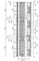
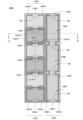
- FIG. 2 is an enlarged view of the pixel layout when the display device 100 is viewed from above
- FIG. 3 is a cross-sectional view of the pixel layout shown in FIG. 2 cut along line A1-A2.
- FIG. 4 is a cross-sectional view of the pixel layout shown in FIG. 2 taken along line B1-B2.
- the configuration of a top emission display device will be described.
- FIG. 2 shows regions in which a pixel 105R having a red light emitting element, a pixel 105G having a green light emitting element, and a pixel 105B having a blue light emitting element are provided.
- the pixel 105R, pixel 105G, and pixel 105B are arranged side by side in the X direction.
- Each of the plurality of pixels 105R, the plurality of pixels 105G, and the plurality of pixels 105B is arranged in stripes along the Y direction.
- the area surrounded by short wavy lines is the area where the pixel electrode 124 is provided.
- the shape of the pixel electrode 124 in plan view is, for example, rectangular.
- a plurality of pixel electrodes 124 are arranged in a matrix in the X direction and the Y direction.
- pixel electrodes 124R, 124G, and 124B are arranged side by side in the X direction.
- the area surrounded by broken lines is the area where the organic insulating layer 126 is provided.
- the organic insulating layer 126 is also called a partition or bank.
- the shape of the organic insulating layer 126 when viewed from above is rectangular.
- the organic insulating layer 126 is arranged so as to cover the ends of the two pixel electrodes 124 adjacent in the Y direction.
- the organic insulating layer 126 is not arranged on two pixel electrodes 124 adjacent in the X direction. That is, the organic insulating layer 126 is arranged in the region where the light emitting elements of the same color are adjacent, and the organic insulating layer 126 is not arranged in the region where the light emitting elements of different colors are adjacent.
- the length of the organic insulating layer 126 in the X direction when viewed in plan is smaller than the length of the pixel electrode 124 in the X direction, but the present invention is not limited to this.
- the length of the organic insulating layer 126 in the X direction may be substantially the same as the length (width) of the pixel electrode 124 in the X direction.
- regions indicated by solid lines are regions where the light-emitting layers 132R, 132G, and 132B are provided.
- the light emitting layer 132R has light emitting layers 132R-1 to 132R-3.
- a plurality of layers formed in the same process are distinguished by numbers such as ⁇ 1, ⁇ 2, ⁇ 3, and the like. Note that when a plurality of layers formed in the same process are described without distinguishing between them, they may not be numbered.
- the light emitting layers 132R-1 to 132R-3 are separated from each other.
- the light emitting layer 132R-1 is arranged on a plurality of pixel electrodes 124R adjacent in the Y direction.
- the light emitting layer 132R-2 is arranged adjacent to the pixel electrode 124R in the X direction.
- the light emitting layer 132R-3 is arranged between the pixel electrode 124R and the pixel electrode 124G. That is, the light emitting layers 132R-1 to 132R-3 extend along the Y direction and are separated in the X direction.
- the light-emitting layer 132R has a region extending along the Y direction on the pixel electrode 124 and a region extending along the Y direction between two adjacent pixel electrodes 124 .
- the light emitting layer 132G has light emitting layers 132G-1 to 132G-3.
- the light emitting layer 132G-1 is arranged on a plurality of pixel electrodes 124G adjacent in the Y direction.
- the light emitting layer 132G-2 is arranged between the pixel electrode 124R and the pixel electrode 124G.
- the light emitting layer 132G-3 is arranged between the pixel electrode 124G and the pixel electrode 124B.
- the light emitting layers 132B-1 to 132B-3 are separated from each other.
- the light-emitting layer 132B-1 is arranged on a plurality of pixel electrodes 124B adjacent in the Y direction.
- the light emitting layer 132B-2 is arranged between the pixel electrode 124G and the pixel electrode 124B.
- the light emitting layer 132B-3 is arranged adjacent to the pixel electrode 124B in the X direction.
- the light-emitting layers 132R-3 and 132G-2 overlap each other, and the light-emitting layers 132G-3 and 132B-2 overlap each other.
- the length (width) of the light emitting layer 132R-1 in the X direction is substantially the same as the length (width) of the pixel electrode 124R in the X direction.
- the length (width) in the X direction of the light emitting layer 132G-1 is substantially the same as the length (width) in the X direction of the pixel electrode 124R.
- the length (width) in the X direction of the light emitting layer 132B-1 is substantially the same as the length (width) in the X direction of the pixel electrode 124R.
- the light-emitting layer 132 is separated into a region overlapping with the pixel electrode 124 and the organic insulating layer 126 and a region adjacent to the pixel electrode 124 .
- the length of the light-emitting layer 132R-1 in the X direction becomes substantially the same as the length of the pixel electrode 124 in the X direction.
- the region where the pixel electrode 124 and the light-emitting layer 132 overlap corresponds to the light-emitting region when the light-emitting element 130 emits light.
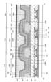
- FIG. 3 shows a cross-sectional view of a plurality of pixels 105B.
- a light emitting element 130B is provided in the pixel 105B.
- the light-emitting region of the light-emitting element 130 is shown as the light-emitting region 120. As shown in FIG.
- a plurality of transistors 110 are provided over the substrate 101 with an insulating film 112 interposed therebetween.
- a pixel circuit is configured by the plurality of transistors 110 .
- a transistor 110 includes at least a semiconductor layer 114 , a gate insulating film 115 , and a gate electrode 116 .
- An interlayer insulating film 121 is provided over the transistor 110 .
- Source or drain electrodes 117 and 118 are provided on the interlayer insulating film 121 .
- Each of source or drain electrodes 117 and 118 is connected to semiconductor layer 114 through a contact hole provided in interlayer insulating film 121 .
- An insulating film 122 is provided on the interlayer insulating film 121 .
- the insulating film 122 can reduce unevenness caused by the transistor 110 and the source or drain electrodes 117 and 118 .
- the plurality of transistors 110 provided over the substrate 101 and the interlayer insulating film 121 and the insulating film 122 provided over the transistors 110 are formed using known materials and methods. 4 and subsequent drawings, the configuration of the pixel circuit provided below the insulating film 122 is the same as that in FIG. 3, so detailed description thereof will be omitted.
- a plurality of pixel electrodes 124B are provided on the insulating film 122 .
- the pixel electrode 124B is electrically connected to the transistor 110 included in the pixel circuit.
- the pixel electrode 124B functions as an anode.
- a highly reflective metal film such as silver is used.
- a transparent conductive layer with a high work function such as an indium oxide-based transparent conductive layer (for example, ITO: Indium Tin Oxide) or a zinc oxide-based transparent conductive layer (for example, IZO: Indium Zinc Oxide, ZnO: Zinc Oxide) is used. may be used.
- ITO Indium Tin Oxide
- IZO Indium Zinc Oxide
- ZnO Zinc Oxide
- An organic insulating layer 126 is provided on the insulating film 122 so as to cover the ends of the pixel electrodes 124B.
- the organic insulating layer 126 is provided at the ends of the two adjacent pixel electrodes 124B.
- the organic insulating layer 126 is arranged so that the organic layer 160 including the light emitting layer 132B provided on the plurality of pixel electrodes 124B is continuously provided without being cut in the plurality of adjacent pixels 105B. be. Therefore, the organic insulating layer 126 preferably slopes gently. Also, the cross section of the upper end of the organic insulating layer 126 is preferably rounded.
- the organic insulating layer 126 can use known organic resin materials such as polyimide, polyamide, acrylic, epoxy, or siloxane. Note that the organic insulating layer 126 is not provided between the pixel electrodes 124B and 124G. Also, the organic insulating layer 126 is not provided between the pixel electrodes 124G and 124R. In other words, the organic insulating layer 126 is provided when the light emitting elements 130 of the same color are continuously arranged in the adjacent pixel electrodes 124 .
- a common layer 128 is provided on the plurality of pixel electrodes 124B and the plurality of organic insulating layers 126 .
- the common layer 128 is commonly provided over the plurality of light emitting elements 130B.
- Common layer 128 includes at least one of a hole transport layer and a hole injection layer.
- a light-emitting layer 132B is provided on the common layer 128 .
- the light emitting layer 132B-1 is commonly provided over the plurality of light emitting elements 130B.
- a common layer 134 is provided on the light emitting layer 132B-1.
- the common layer 134 is commonly provided over the plurality of light emitting elements 130B.
- Common layer 134 includes at least one of an electron transport layer and an electron injection layer.
- organic layers 160 include common layer 128 , light emitting layer 132 , and common layer 134 .
- a counter electrode 136 is provided on the common layer 134 .
- the counter electrode 136 is commonly provided over the plurality of light emitting elements 130B.
- a light-transmitting electrode is used as the counter electrode 136 .
- a MgAg thin film or a transparent conductive layer (ITO or IZO) is used as the counter electrode 136 .
- a sealing film 150 is provided on the counter electrode 136 .
- the sealing film 150 has an inorganic insulating film 151 , an organic insulating film 152 and an inorganic insulating film 153 .
- the inorganic insulating film 151 and the inorganic insulating film 153 can prevent moisture from entering the light emitting element 130 .
- the organic insulating film 152 between the inorganic insulating film 151 and the inorganic insulating film 153 cracking of the sealing film 150 can be suppressed.
- the inorganic insulating film 151 and the inorganic insulating film 153 are in contact with each other, which is preferable because the sealing function against moisture is improved.
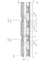
- FIG. 4 shows a cross-sectional view of pixels 105R, 105G, and 105B.
- the pixel 105R is provided with the light emitting element 130R
- the pixel 105G is provided with the light emitting element 130G
- the pixel 105B is provided with the light emitting element 130B.
- the light emitting regions of the light emitting elements 130R, 130G and 130B are shown as light emitting regions 120R, 120G and 120B.
- Pixel electrodes 124 R, 124 G, and 124 B are provided on the insulating film 122 .
- a common layer 128 is provided on the pixel electrodes 124R, 124G, and 124B. In FIG. 4, the common layer 128 is separated by the top edges of the pixel electrodes 124R, 124G, 124B. Therefore, the common layer 128 is composed of common layers 128-1 to 128-7.
- a common layer 128-2 is provided on the pixel electrode 124R, a common layer 128-4 is provided on the pixel electrode 124G, and a common layer 128-6 is provided on the pixel electrode 124B.
- the common layer 128-1 is provided adjacent to the pixel electrode 124R in the X direction.
- the common layer 128-3 is provided between the pixel electrode 124R and the pixel electrode 124G.
- a common layer 128-5 is provided between the pixel electrode 124G and the pixel electrode 124B.
- the common layer 128-7 is provided adjacent to the pixel electrode 124B in the X direction.
- the film thickness of the pixel electrode 124 is larger than the film thickness of the common layer 128 . Therefore, when forming the common layer 128 on the pixel electrode 124 by vapor deposition, the common layer 128 is less likely to adhere to the side surfaces of the pixel electrode 124 . Thereby, the common layer 128 can be separated at the upper end portion of the pixel electrode 124 .
- the film thickness of the pixel electrode 124 is, for example, 60 nm or more and 350 nm or less.
- the thickness of the common layer 128 is, for example, in the range of 30 nm to 150 nm and less than the thickness of the pixel electrode 124 .
- the thickness of the common layer 128 may vary according to the color of light emitted by the light emitting device 130 . That is, the thickness of the common layer 128-2, the thickness of the common layer 128-4, and the thickness of the common layer 128-6 may be different. Even in this case, the thickness of the pixel electrodes 124R, 124G and 124B is preferably larger than the thickness of the common layers 128-2, 128-4 and 128-6.
- the common layer 128 includes a hole injection layer provided in contact with the pixel electrode 124 and a hole transport layer laminated thereon. At this time, if the film thickness of the hole injection layer is smaller than the film thickness of the pixel electrode 124 , the total thickness of the common layer 128 including the lamination of the hole injection layer and the hole transport layer may exceed the pixel electrode 124 .
- the common layer 128 it is desirable for the common layer 128 to be divided over the entire layer, but the hole injection layer in the common layer 128 improves the efficiency of hole injection from the pixel electrode 124 .
- the resistance can be relatively low due to the action of the dopant added for the purpose. Therefore, by dividing the layer by the upper end portion of the pixel electrode 124, the leakage current in the horizontal direction can be reduced.
- the film thickness of the pixel electrode 124 is, for example, 60 nm or more and 350 nm or less.
- the thickness of the common layer 128 is, for example, in the range of 100 nm to 150 nm and less than the thickness of the pixel electrode 124.
- the thickness of the hole injection layer provided in contact with the pixel electrode 124 is, for example, The thickness should be 10 nm or more and 30 nm or less.
- light emitting layers 132R-1 to 132R-3 On the common layer 128, light emitting layers 132R-1 to 132R-3, light emitting layers 132G-1 to 132G-3, and light emitting layers 132B-1 to 132B-3 are provided.
- Light-emitting layer 132R-1 is provided on common layer 128-2
- light-emitting layer 132G-1 is provided on common layer 128-4
- light-emitting layer 132B-1 is provided on common layer 128-6.
- Light-emitting layer 132R-2 is provided on common layer 128-1
- light-emitting layer 132R-3 and light-emitting layer 132G-2 are provided on common layer 128-3
- light-emitting layer 132G-3 and light-emitting layer 132B- 2 is provided on common layer 128-5.
- the sum of the film thickness of the pixel electrode 124 and the film thickness of the common layer 128 is larger than the film thickness of the light emitting layer 132 . Therefore, when the light-emitting layer 132 is formed on the common layer 128 by vapor deposition, the light-emitting layer 132 is less likely to adhere to the side surfaces of the pixel electrodes 124 and the common layer 128 . Thereby, the light emitting layer 132 can be separated at the upper end portion of the common layer.
- the film thickness of the light emitting layer 132 is 10 nm or more and 50 nm or less.
- the film thickness of the light emitting layer 132 may vary depending on the color of light emitted from the light emitting element 130 . Even in this case, the sum of the film thickness of the pixel electrode 124 and the film thickness of the common layer 128 is preferably larger than the film thickness of the light-emitting layer 132 .
- a common layer 134 is provided on the light-emitting layers 132R, 132G, and 132B. Common layer 134 is separated by light emitting layers 132R-1, 132G-1, 132B-1. Therefore, the common layer 134 is composed of common layers 134-1 to 134-7.
- a common layer 134-2 is provided on the light-emitting layer 132R-1
- a common layer 134-4 is provided on the light-emitting layer 132G-1
- a common layer 134-6 is provided on the light-emitting layer 132B-1. is provided.
- the common layer 134-1 is provided adjacent to the pixel electrode 124R. Also, the common layer 134-3 is provided between the pixel electrode 124R and the pixel electrode 124G.
- a common layer 134-5 is provided between the pixel electrode 124G and the pixel electrode 124B.
- the common layer 134-7 is provided adjacent to the pixel electrode 124B in the X direction.
- a counter electrode 136 is provided on the common layer 134 .
- the counter electrodes 136 are separated by common layers 134-2, 134-4, 134-6. Therefore, the counter electrode 136 is composed of counter electrodes 136-1 to 136-7.
- a counter electrode 136-2 is provided on the common layer 134-2
- a counter electrode 136-4 is provided on the common layer 134-4
- a counter electrode 136-6 is provided on the common layer 134-6.
- the counter electrode 136-1 is provided adjacent to the pixel electrode 124R.
- the counter electrode 136-3 is provided between the pixel electrode 124R and the pixel electrode 124G.
- the counter electrode 136-5 is provided between the pixel electrode 124G and the pixel electrode 124B.
- the counter electrode 136-7 is provided adjacent to the pixel electrode 124B in the X direction.
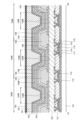
- FIG. 24 omits the illustration of the configuration of the pixel circuit provided below the insulating film 222 .
- FIG. 24 shows a cross-sectional view of pixels 205R, 205G, and 205B in a conventional display device.
- the pixel 205R is provided with the light emitting element 230R
- the pixel 205G is provided with the light emitting element 230G
- the pixel 205B is provided with the light emitting element 230B.
- the light-emitting element 230R has at least a pixel electrode 224R, a light-emitting layer 232R, and a counter electrode 236.
- the light emitting element 230G has at least a pixel electrode 224G, a light emitting layer 232G, and a counter electrode 236. As shown in FIG.
- the light-emitting element 230B has at least a pixel electrode 224B, a light-emitting layer 232B, and a counter electrode 236.
- FIG. A common layer 228 is provided between the pixel electrodes 224R, 224G, 224B and the light emitting layers 232R, 232G, 232B.
- a common layer 234 is provided between the light emitting layers 232R, 232G, 232B and the counter electrode 236. As shown in FIG. The common layers 228 and 234 are commonly provided over the light emitting elements 230R, 230G and 230B (over the display area). In FIG.
- the pixel electrodes 224R, 224G, 224B are anodes and the counter electrode 236 is a cathode.
- common layer 228 includes at least one of a hole transport layer and a hole injection layer
- common layer 234 includes at least one of an electron transport layer and an electron injection layer.
- the ends of the pixel electrodes 224R, 224G, and 224B are covered with an insulating layer 226. Further, openings 220R, 220G and 220B are provided in the insulating layer 226 so as to expose the pixel electrodes 224R, 224G and 224B. The openings 220R, 220G, and 220B correspond to light emitting regions in the light emitting element.
- a light-emitting layer 232B and a light-emitting layer 232R are provided on the common layer 228 on the insulating layer 226 . Part of the light emitting layer 232B overlaps part of the light emitting layer 232R.
- the light emission start voltage of the light emitting layer 232B is higher than the light emission start voltages of the light emitting layers 228R and 232G. Therefore, when the light-emitting element 230B emits light, a large voltage is applied to the light-emitting layer 232B, and holes in the common layer 228 laterally move from the pixel 205B toward the pixels 205R and 205G.
- the light-emitting layer 232B When the light-emitting layer 232B exhibits hole-transport properties, holes pass through the light-emitting layer 232B in the thickness direction. Therefore, the light emitting layer 232R and the light emitting layer 232G emit light at the end of the light emitting layer 232R. Alternatively, when the light-emitting layer 232B exhibits an electron-transport property, holes do not pass through the thickness direction of the light-emitting layer 232B, but move laterally. Therefore, the light emitting layer 232R emits light near the edge of the light emitting layer 232B.
- the light emission start voltage of the light emitting layer 232R and the light emission start voltage of the light emitting layer 232G are approximately the same.
- lateral leakage current may cause adjacent pixels to emit light, degrading the display characteristics of the EL display device.
- the regions provided with the light-emitting layers 232 may be formed apart from each other so as not to overlap each other.
- the openings 220R, 220G, and 220B must be formed sufficiently apart from each other, and the definition is reduced. There is a problem of lowering.
- the common layer 128 is separated so as to extend in the Y direction. Specifically, the common layer 128 is separated by utilizing the coverage of the organic material at the edge of the pixel electrode 124 . This separates the common layer 128 between the different color pixels 105R, 105G, 105B. Therefore, lateral leakage current can be suppressed from flowing through the common layer 128 . Accordingly, it is possible to suppress unintended light emission between the pixels 105R, 105G, and 105B of different colors, so that the display characteristics of the EL display device can be improved.
- the region where the light emitting element emits light is limited to the region where the pixel electrode 124 is provided, so that unintended light emission can be further suppressed.
- the common layers 128 and 134 and the counter electrode 136 also extend along the Y direction and are separated in the X direction, similarly to the light emitting layer 132 . That is, the common layers 128 and 134 and the counter electrode 136 are divided into regions extending along the Y direction on the pixel electrodes 124 adjacent to each other in the Y direction and regions extending in the Y direction between two pixel electrodes 124 adjacent to each other in the X direction. and a region extending along.
- the organic layer 160 and the counter electrode 136 may be connected to each other in regions extending along the Y direction in the peripheral region 103 .
- the common layers 128-1 to 128-7 may be separated from each other in regions extending along the Y direction in the display region 102, and may extend along the Y direction in the peripheral region 103. regions may be connected to each other.
- the counter electrodes 136-1 to 136-7 may be separated from each other in regions extending along the Y direction in the display region 102, and may extend along the Y direction in the peripheral region 103. regions may be connected to each other.
- the common layer 128 that causes the lateral leakage current to flow. Therefore, at least the common layers 128 need only extend along the Y direction and be separated in the X direction.
- the common layer 134 and the counter electrode 136 may be provided continuously over the entire display area 102 . If at least the common layers 128 extend along the Y direction and are separated in the X direction, it is possible to suppress lateral leakage current from flowing through the common layers 128 .
- FIG. 5 to 11 the manufacturing method of the configuration corresponding to the cross-sectional view taken along the line B1-B2 shown in FIG. 2 will be described unless otherwise specified.
- a transistor 110 forming a pixel circuit is provided on a substrate 101.
- An interlayer insulating film 121 containing at least one of silicon oxide and silicon nitride is formed over the transistor 110 .
- Source or drain electrodes 117 and 118 are formed on the interlayer insulating film 121 .
- An insulating film 122 is formed on the interlayer insulating film 121 .
- the insulating film 122 functions as a planarizing film.
- the insulating film 122 is composed of an organic resin material.
- organic resin material known organic resin materials such as polyimide, polyamide, acrylic, epoxy, or siloxane can be used.
- the insulating film 122 By providing the insulating film 122 over the transistor 110 or the interlayer insulating film 121, unevenness of the transistor can be reduced.
- Contact holes are formed in the insulating film 122 to partially expose the source or drain electrodes 117 and 118 . The contact hole is for connecting the pixel electrode 124 to be formed in the next step and the source or drain electrode 117 .
- FIG. 5 is a diagram for explaining the steps of forming the insulating film 122 and the pixel electrodes 124R, 124G, and 124B.
- the pixel electrodes 124R, 124G, and 124B are formed by vapor deposition using metal masks. Each of the pixel electrodes 124 R, 124 G, and 124 B is electrically connected to the source or drain electrode 117 connected to the transistor 110 through contact holes provided in the insulating film 122 .
- the pixel electrodes 124R, 124G, and 124B function as anodes.
- the film thickness of the pixel electrode 124 is preferably, for example, 60 nm or more and 350 nm or less.
- the pixel electrodes 124R, 124G, and 124B are formed with a three-layer structure of lower ITO, Ag, and upper ITO layers will be described.
- the thickness of the lower layer ITO is 5 nm or more and 100 nm or less
- the thickness of Ag is 50 nm or more and 200 nm or less
- the thickness of the upper layer ITO is 5 nm or more and 50 nm or less.
- FIG. 6 is a diagram for explaining the process of forming a plurality of organic insulating layers 126.
- FIG. 6 corresponds to a cross-sectional view taken along line A1-A2 shown in FIG.
- an organic insulating layer 126 is provided between pixel electrodes 124 adjacent in the Y direction.
- the organic insulating layer 126 is provided so as to cover the edges of the adjacent pixel electrodes 124 .
- the organic insulating layer 126 is composed of an organic resin material.
- the organic insulating layer 126 is not formed between the pixel electrodes 124R and 124G, between the pixel electrodes 124G and 124B, and between the pixel electrodes 124B and 124R.
- organic resin material known organic resin materials such as polyimide, polyamide, acrylic, epoxy, or siloxane can be used.
- FIG. 7 is a diagram for explaining the steps of forming the common layer 128 and the light emitting layer 132R.
- Common layers 128-1 to 128-7 are formed on the pixel electrodes 124R, 124G and 124B.
- Common layers 128-1 to 128-7 include at least one of a hole transport layer and a hole injection layer. Known materials may be appropriately used for the hole transport layer and the hole injection layer.
- the common layer 128 is formed on the pixel electrode 124 by vapor deposition, the common layer 128 overhangs when the common layer 128 is deposited on the pixel electrode 124 .
- the common layer 128 is less likely to adhere to the side surface of the pixel electrode 124, and the common layer 128 is more likely to break. Thereby, the common layer 128 can be separated at the upper end portion of the pixel electrode 124 .
- FIG. 8 is a plan view after forming the common layer 128.
- the common layers 128-1 to 128-7 are each separated in the X direction. Also, the common layers 128-1 to 128-7 each extend in the Y direction.
- the common layers 128-2, 128-4, 128-6 overlap the pixel electrodes 124 and the organic insulating layer 126.
- FIG. The common layers 128-1, 128-3, 128-5, 128-7 do not overlap the pixel electrodes 124.
- a light emitting layer 132R is formed on the common layers 128-1 to 128-3.
- the light-emitting layer 132R overhangs when the light-emitting layer 132R is deposited on the common layer 128-2. Since the overhanging portion has an eaves structure, the light emitting layer 132R is less likely to stick to the side surfaces of the common layer 28-2 and the pixel electrode 124R, and the light emitting layer 132R is more likely to be disconnected. Thereby, the light emitting layer 132R can be separated at the upper end portion of the common layer 128-2. Thus, light emitting layers 132R-1 to 132R-3 are formed.
- FIG. 9 is an enlarged view of the area 170 shown in FIG. 9, the pixel electrode 124 has a three-layer structure of a transparent conductive layer 141, a metal layer 142, and a transparent conductive layer 143.
- the transparent conductive layers 141 and 143 may protrude beyond the edge of the metal layer 142 . Since the end portion of the transparent conductive layer 143 has a canopy structure, the common layer 128 is less likely to stick to the side surface of the pixel electrode 124, and the common layer 128 is more likely to be cut off.
- the common layer 128 can be separated at the end of the transparent conductive layer 143 .
- the step disconnection of the common layer 128 can be reliably performed at the upper end portion of the pixel electrode 124 .
- the light-emitting layer 132R is formed on the common layer 128, the light-emitting layer 132R can be reliably cut off at the upper end of the common layer 128-2.
- FIG. 10 is a diagram explaining the process of forming the light emitting layers 132G and 132B.
- the method for forming the light emitting layers 132G and 132B is the same as the method for forming the light emitting layer 132R.
- a light-emitting layer 132G is formed on the common layers 128-3 to 128-5 by vapor deposition.
- the light emitting layers 132G-1 to 132G-3 are formed by separating the light emitting layer 132G at the ends of the common layer 128-4.
- a light-emitting layer 132B is formed on the common layers 128-5 to 128-7 by vapor deposition.
- the light emitting layers 132B-1 to 132B-3 are formed by separating the light emitting layer 132B at the ends of the common layer 128-6.
- FIG. 11A and 11B are diagrams for explaining the steps of forming the common layer 134 and the counter electrode 136.
- FIG. Common layers 134-1 to 134-7 are formed on the light emitting layers 132R, 132G, and 132B.
- Common layers 134-1 to 134-7 include at least one of an electron transport layer and an electron injection layer. Known materials may be appropriately used for the electron-transporting layer and the electron-injecting layer.
- the common layer 134 is formed on the light-emitting layers 132R, 132G, and 132B by vapor deposition, the common layer 134 is separated at the ends of the light-emitting layers 132R-1, 132G-1, and 132B-1.
- Common layers 134-1 to 134-7 are thus formed. Note that the plan view after the formation of the common layer 134 is the same as FIG. 8, so the illustration is omitted.
- a counter electrode 136 is formed on the common layer 134 .
- a light-transmitting material may be used as appropriate for the counter electrode 137 .
- the counter electrodes 136 are formed on the common layer 134, the counter electrodes 136-1 to 136- are separated at the ends of the common layers 134-2, 134-4, and 134-6. 7 is formed.
- the plan view after forming the counter electrode 136 is the same as FIG. 8, so the illustration is omitted.
- a sealing film 150 is formed on the counter electrode 136 .
- the sealing film 150 is formed of an inorganic insulating film 151, an organic insulating film 152, and an inorganic insulating film 153 in this order. It is preferable that the inorganic insulating film 151 is not separated on the counter electrode 136 .
- the film thickness of the inorganic insulating film 151 is preferably a film thickness that alleviates unevenness formed by the light emitting element 130 .
- the inorganic insulating film 151 may be thicker than the inorganic insulating film 153 .
- the display device 100 shown in FIGS. 2 to 4 can be manufactured.
- the pixels 105R, 105G, and 105B emitting light of different colors are formed by separating the common layer 128, and a plurality of pixels emitting light of the same color are formed.
- a common layer 128 is formed continuously.
- the present invention is not limited to this. There is no limitation on the formation order of the light emitting layers 132R, 132G, and 132B.
- FIGS. 2 and 8 show views in which common layers 128-1 and 128-2 are separated from each other, and common layers 128-2 and 128-3 are separated from each other.
- the common layer 128-2 may be connected to the common layer 128-1 or the common layer 128-3 in a region adjacent to the organic insulating layer 126.
- FIG. Since the side surfaces of the organic insulating layer 126 have a gentle slope, the common layers 128-1, 128-2, and 128-3 may not be separated in the regions adjacent to the organic insulating layer 126.
- FIG. 12 is a plan view of a display device 100A according to one embodiment of the invention.
- the planar layout of the organic layer 160 including the light-emitting layer 132 is the same as in FIGS. 2 and 8, so the illustration is omitted.
- an inorganic insulating layer 138 is provided on the pixel electrodes 124R, 124G, 124B and the organic insulating layer 126. As shown in FIG. The inorganic insulating layer 138 is provided so as to cover peripheral portions of the pixel electrodes 124R, 124G, and 124B. In other words, the inorganic insulating layer 138 is provided with an opening so as to expose the surface of the pixel electrode 124R. The inorganic insulating layer 138 is provided so as to overlap with the organic insulating layer 126 .
- the inorganic insulating layer 138 is made of, for example, a silicon nitride film. The film thickness of the inorganic insulating layer 138 is, for example, 50 nm or more and 500 nm or less.
- FIG. 13 is a cross-sectional view taken along line A1-A2 shown in FIG.
- inorganic insulating layer 138 covers organic insulating layer 126 . Therefore, the organic layer 160 is provided on the pixel electrode 124 and the inorganic insulating layer 138 .
- the pixel electrode 124 and the common layer 128 are in contact with each other at the opening of the inorganic insulating layer 138 .
- the opening of the inorganic insulating layer 138 becomes the light emitting region of the light emitting element 130 .
- FIG. 14 is a cross-sectional view taken along line B1-B2 shown in FIG.
- the inorganic insulating layer 138 covers peripheral portions of the pixel electrodes 124R, 124G, and 124B.
- a common layer 128 is provided on the pixel electrodes 124R, 124G, 124B and the inorganic insulating layer 138.
- the film thickness of the pixel electrode 124 is greater than the film thickness of the common layer 128 .
- An inorganic insulating layer 138 is provided on the side surface of the pixel electrode 124 .
- FIG. 15 is an enlarged view of the area 170A shown in FIG.
- the pixel electrode 124 has a three-layer structure of a transparent conductive layer 141 , a metal layer 142 and a transparent conductive layer 143 .
- the transparent conductive layers 141 and 143 may protrude beyond the edge of the metal layer 142 .
- the inorganic insulating layer 138 is formed by sputtering, for example.
- the inorganic insulating layer 138 is also formed on the side surfaces of the transparent conductive layer 141 , the metal layer 142 and the transparent conductive layer 143 .
- the film thickness of the inorganic insulating layer 138 is added to the film thickness of the pixel electrode 124 . Therefore, when the common layer 128 is formed on the pixel electrode 124 and the inorganic insulating layer 138 by vapor deposition, the ends of the inorganic insulating layer 138 are more likely to protrude.
- the common layer 128 is less likely to adhere to the side surface of the inorganic insulating layer 138, and the common layer 128 is more likely to be cut off. Thereby, the common layer 128 can be separated at the upper end portion of the pixel electrode 124 .
- the inorganic insulating layer 138 covers the side surfaces of the pixel electrodes 124 . This can prevent electrical connection between the pixel electrode 124 and the organic layer 160 provided between two adjacent pixel electrodes 124 .
- FIG. 16 is a plan view of a display device 100B according to one embodiment of the invention.
- the planar layout of the organic layer 160 including the light-emitting layer 132 is the same as in FIGS. 2 and 8, so the illustration is omitted.
- the stacking order of the organic insulating layer 126 and the inorganic insulating layer 138 is different.
- the inorganic insulating layer 138 is provided on the pixel electrodes 124R, 124G and 124B. Also, the organic insulating layer 126 is provided on the pixel electrodes 124R, 124G, 124B and the inorganic insulating layer 138.
- FIG. The inorganic insulating layer 138 is provided so as to cover peripheral portions of the pixel electrodes 124R, 124G, and 124B. In other words, the inorganic insulating layer 138 is provided with an opening so as to expose the surface of the pixel electrode 124R.
- the inorganic insulating layer 138 is provided so as to overlap with the organic insulating layer 126 .
- the inorganic insulating layer 138 is made of, for example, a silicon nitride film. The film thickness of the inorganic insulating layer 138 is, for example, 50 nm or more and 500 nm or less.
- FIG. 17 is a cross-sectional view taken along line A1-A2 shown in FIG.
- the inorganic insulating layer 138 covers peripheral portions of the pixel electrodes 124R, 124G, and 124B.
- a common layer 128 is provided on the pixel electrodes 124 R, 124 G, 124 B and the organic insulating layer 126 .
- a cross-sectional view taken along line B1-B2 shown in FIG. 16 is similar to FIG. 14, so detailed description thereof will be omitted.
- the inorganic insulating layer 138 covers the side surfaces of the pixel electrodes 124 . This can prevent electrical connection between the pixel electrode 124 and the organic layer 160 provided between two adjacent pixel electrodes 124 .
- FIG. 18 is an enlarged view of the pixel layout when the display device 100C is viewed from above, and FIG. 19 is a cross-sectional view of the pixel layout shown in FIG. 18 cut along line C1-C2.
- FIG. 20 is a cross-sectional view of the pixel layout shown in FIG. 18 taken along line D1-D2.
- pixels 105R and pixels 105G are alternately arranged in the Y direction.
- the pixels 105B are arranged side by side in the Y direction.
- the pixel 105R is arranged adjacent to the pixel 105B in the X direction.
- the pixel 105G is arranged adjacent to the pixel 105B in the X direction.
- the organic insulating layer 126 is arranged so as to cover the edge of the pixel electrode 124R and the edge of the pixel electrode 124G that are adjacent in the Y direction. Also, the organic insulating layer 126 is arranged so as to cover the end portions of the two pixel electrodes 124B adjacent in the Y direction and the end portions of the pixel electrodes 124B. The organic insulating layer 126 is not arranged between the two pixel electrodes 124R and 124B that are adjacent in the X direction. Also, the organic insulating layer 126 is not arranged between the two pixel electrodes 124G and the pixel electrode 124B that are adjacent in the X direction.
- the light emitting layer 132R has light emitting layers 132R-1 to 132R-3. Each of the light emitting layers 132R-1 to 132R-3 is separated. A light-emitting layer 132R-1 is disposed on the pixel electrode 124R. The light emitting layer 132R-2 is arranged adjacent to the pixel electrode 124R. The light emitting layer 132R-3 is arranged between the pixel electrode 124R and the pixel electrode 124B. The light emitting layer 132G has light emitting layers 132G-1 to 132G-3. A light-emitting layer 132G-1 is disposed on the pixel electrode 124G. The light emitting layer 132G-2 is arranged adjacent to the pixel electrode 124G.
- the light emitting layer 132G-3 is arranged between the pixel electrode 124G and the pixel electrode 124B.
- the light emitting layers 132B-1 to 132B-3 are separated from each other.
- the light-emitting layer 132B-1 is arranged on a plurality of pixel electrodes 124B adjacent in the Y direction.
- the light emitting layer 132B-2 is arranged between the pixel electrodes 124R, 124G and the pixel electrode 124B.
- the light emitting layer 132B-3 is arranged adjacent to the pixel electrode 124B. Although not shown, the light emitting layers 132R-2 and 132G-3 overlap the light emitting layer 132B-3.
- the light-emitting layers 132R-3 and 132G-3 overlap with the light-emitting layer 132B-2. Also, the light-emitting layer 132R-1 overlaps the light-emitting layer 132G-1 on the organic insulating layer 126. FIG.
- FIG. 19 the cross-sectional view when the pixel 105G and the pixel 105B are adjacent to each other is substantially the same as FIG. 14, so for detailed description, refer to the description regarding FIG.
- FIG. 20 shows the case where the pixel 105R and the pixel 105G are adjacent to each other.
- the light-emitting layer 132R-1 and the light-emitting layer 132G-1 overlap each other on the organic insulating layer 126.
- FIG. 20 shows the case where the pixel 105R and the pixel 105G are adjacent to each other.
- the light-emitting layer 132R-1 and the light-emitting layer 132G-1 overlap each other on the organic insulating layer 126.
- the light emitting element 130B has a higher light emission start voltage than the light emitting elements 130R and 130G. Therefore, in a region where the light emitting element 130B and the light emitting elements 130R and 130G are adjacent to each other, the voltage of the light emitting element 130B may cause unintended light emission of the light emitting elements 130R and 130G.
- the light emitting layer 132 is separated at the edge of the pixel electrode 124 . Therefore, the overlapping regions of the light emitting layer 132B and the light emitting layers 132R and 132G are less susceptible to the voltage applied to the pixel electrode 124. FIG. Therefore, it is possible to suppress the flow of the lateral leak current, so that the display quality can be improved.
- the light emission start voltage of the light emitting element 130R and the light emission start voltage of the light emitting element 130G are approximately the same. Therefore, even if either the light emitting element 130R or the light emitting element 130G emits light, the influence of the lateral leakage current from the light emitting layer 132R-1 or the light emitting layer 132G-1 is small. Therefore, on the organic insulating layer 126, there may be a region where the light emitting layer 132R-1 and the light emitting layer 132G-1 overlap each other.
- a display device 100D obtained by reversing the stacking order of the pixel electrode 124 and the counter electrode 136 in the display devices 100, 100A to 100C according to the previous embodiments will be described with reference to FIGS.
- FIG. 21 is an enlarged view of the pixel layout when the display device 100 is viewed from above
- FIG. 22 is a cross-sectional view of the pixel layout shown in FIG. 21 taken along line E1-E2.
- FIG. 23 is a cross-sectional view of the pixel layout shown in FIG. 21 taken along line F1-F2.
- the display device 100D differs from the display device 100 in that the pixel electrodes 124R, 124G, and 124B function as cathodes, and the counter electrode 136 functions as an anode.
- regions surrounded by short wavy lines are regions where the pixel electrodes 136R, 136G, and 136B are provided.
- the material of the counter electrode 136 described in the first embodiment may be used.
- the material of the pixel electrode 124 described in the first embodiment may be used.
- the pixel electrodes 124R, 124G, and 124B are each electrically connected to the transistor 110 included in the pixel circuit.
- the common layer 134 provided between the pixel electrodes 124R, 124G, 124B and the light emitting layers 132R, 132G, 132B includes at least one of an electron transport layer and an electron injection layer.
- a common layer 128 provided between the counter electrode 136 and the light emitting layers 132R, 132G, and 132B includes at least one of a hole transport layer and a hole injection layer.
- Pixel electrodes 124 R, 124 G, and 124 B are provided on the insulating film 122 .
- a common layer 134 is provided on the pixel electrodes 124R, 124G, and 124B. In FIG. 22, the common layer 134 is separated by the top edges of the pixel electrodes 124R, 136G, 136B. Therefore, the common layer 134 is composed of common layers 134-1 to 134-7.
- a common layer 134-2 is provided on the pixel electrode 124R, a common layer 134-4 is provided on the pixel electrode 124G, and a common layer 134-6 is provided on the pixel electrode 124B.
- the common layer 134-1 is provided adjacent to the pixel electrode 124R in the X direction.
- the common layer 134-3 is provided between the pixel electrode 124R and the pixel electrode 124G.
- a common layer 134-5 is provided between the pixel electrode 124G and the pixel electrode 124B.
- the common layer 134-7 is provided adjacent to the pixel electrode 124B in the X direction.
- the film thickness of the pixel electrode 124 is larger than the film thickness of the common layer 134 . Therefore, when forming the common layer 134 on the pixel electrode 124 by vapor deposition, the common layer 134 is less likely to adhere to the side surfaces of the pixel electrode 124 . Thereby, the common layer 134 can be separated at the upper end portion of the pixel electrode 124 .
- the film thickness of the pixel electrode 124 is, for example, 60 nm or more and 350 nm or less.
- the thickness of the common layer 134 is, for example, in the range of 30 nm to 150 nm and less than the thickness of the pixel electrode 124 .
- the light-emitting layers 132R, 132G, 132B are separated by upper ends of common layers 134-2, 134-4, 134-6, respectively.
- the light-emitting layer 132R has light-emitting layers 132R-1 to 132R-3
- the light-emitting layer 132G has light-emitting layers 132G-1 to 132G-3
- the light-emitting layer 132B has light-emitting layers 132B-1 to 132B-3.
- Common layer 128 is separated by the tops of light emitting layers 132R-1, 132G-1, 132B-1, respectively.
- Common layer 128 has common layers 128-1 through 128-7.
- the counter electrodes 136 are separated by upper edges of common layers 128-2, 128-4, 128-6, respectively.
- the counter electrode 136 has counter electrodes 136-1 to 124-6.
- the light emitting element 130 uses the pixel electrode 124 as a cathode and the counter electrode 136 as an anode. Even in this case, at least the common layer 134 is separated so as to extend in the Y direction between the pixels 105R, 105G, and 105B of different colors. Specifically, the common layer 134 is separated by utilizing the coverage of the organic material at the edge of the pixel electrode 124 . This separates the common layer 134 between the different color pixels 105R, 105G, 105B. Therefore, lateral leakage current can be suppressed from flowing through the common layer 134 . Accordingly, it is possible to suppress unintended light emission between the pixels 105R, 105G, and 105B of different colors, so that the display characteristics of the EL display device can be improved.
- the common layer 134 includes an electron injection layer provided in contact with the pixel electrode 124 and an electron transport layer laminated thereon. At this time, if the thickness of the electron injection layer is smaller than the thickness of the pixel electrode 124 , the total thickness of the common layer 134 including the lamination of the electron injection layer and the electron transport layer may exceed the thickness of the pixel electrode 124 . Of course, as mentioned above, it is desirable for the common layer 134 to be divided over the entire layer.
- the layer is divided by the upper end portion of the pixel electrode 128, whereby lateral leakage current can be reduced.
- the film thickness of the pixel electrode 124 is, for example, 60 nm or more and 350 nm or less.
- the thickness of the common layer 128 is, for example, in the range of 100 nm to 150 nm and less than the thickness of the pixel electrode 124.
- the thickness of the electron injection layer provided in contact with the pixel electrode 124 is, for example, The thickness should be 0.1 nm or more and 10 nm or less.
- the configuration of the display device 100D according to this embodiment can be applied to the configurations of the display devices 100 and 100A to 100C according to the previous embodiments. That is, in the display devices 100, 100A to 100C, the pixel electrode 124 may be used as the cathode and the counter electrode 136 may be used as the anode.
- the common layer 134 provided between the pixel electrode 124 and the light emitting layer 132 should include at least one of an electron transport layer and an electron injection layer.
- the common layer 128 provided between the counter electrode 136 and the light emitting layer 132 may include at least one of a hole transport layer and a hole injection layer.
- the display device according to one embodiment of the present invention can be applied to various forms. Therefore, based on the display devices 100 and 100A to 100D described as the embodiments and modifications of the invention, those skilled in the art may appropriately add, delete, or change the design of components, or add, omit, or modify processes. Modified conditions are also included in the scope of the present invention as long as they are provided with the gist of the present invention. Moreover, each embodiment described above can be combined with each other as long as there is no technical contradiction.
- the structure for suppressing leakage current in the organic layer 160 in a display device having an organic EL element as a display element has been mainly described.
- An embodiment of the present invention can be applied not only to a display device but also to a photosensor device or the like configured by arranging organic photodiodes in which an organic layer is sandwiched between electrodes in a matrix. Specifically, it can be applied to the overlapping relationship at the end of the organic layers forming the organic photodiode which are separately formed.
- 100, 100A to 100C display device, 101: substrate, 102: display area, 103: peripheral area, 104: scanning line driving circuit, 105: pixel, 105B: pixel, 105G: pixel, 105R: pixel, 106: driver IC , 107: terminal, 108: flexible printed circuit, 110: transistor, 111: scanning line, 112: insulating film, 113: data line, 114: semiconductor layer, 115: gate insulating film, 116: gate electrode, 117: source electrode or drain electrode, 118: source electrode or drain electrode, 121: interlayer insulating film, 122: insulating film, 124, 124B, 124G, 124R: pixel electrode, 126: organic insulating layer, 128, 128-1 to 128-7: Common layer 130: Light emitting element 130B: Light emitting element 130G: Light emitting element 130R: Light emitting element 132: Light emitting layer 132B, 132B-1 to 132B-3: Light emitting layer
Landscapes
- Physics & Mathematics (AREA)
- Optics & Photonics (AREA)
- Engineering & Computer Science (AREA)
- General Physics & Mathematics (AREA)
- Theoretical Computer Science (AREA)
- Microelectronics & Electronic Packaging (AREA)
- Electroluminescent Light Sources (AREA)
Abstract
表示装置は、絶縁表面に設けられた第1画素電極と、第1方向に、第1画素電極と離間して設けられた第2画素電極と、第1方向と交差する第2方向に、第1画素電極と離間して設けられた第3画素電極と、第1方向において、第1画素電極の一部と第2画素電極の一部と重畳する有機絶縁層と、第1画素電極、第2画素電極、第3画素電極、及び有機絶縁層の上に設けられた第1共通層と、第1共通層の上に設けられ、第1画素電極、第2画素電極、有機絶縁層に重畳して連続的に設けられた第1発光層と、第1共通層の上に設けられ、第3画素電極に重畳して設けられた第2発光層と、第1発光層及び第2発光層の上に設けられた対向電極と、を有し、第1共通層は、第1画素電極と重畳する第1領域と、第1画素電極と第3画素電極との間に設けられた第2領域と、第3画素電極と重畳する第3領域と、を有し、第2領域は、第1領域及び第3領域のそれぞれと分離されている。
Description
本発明の一実施形態は、表示装置及びその製造方法に関する。
従来から、表示装置として、有機エレクトロルミネッセンス材料(有機EL材料)を表示部の発光素子(有機EL素子)に用いた有機EL表示装置(Organic Electroluminescence Display)が知られている。近年、有機EL表示装置において、高精細化への要求が高まっている。
有機EL表示装置では、有機EL層をメタルマスクで蒸着して形成する。このとき、各色の蒸着膜が互いに重なり合う場合、異なる色の画素間で横方向のリーク電流が流れてしまうことがある。EL表示装置において、横方向のリーク電流は、隣接する画素を発光させ、EL表示装置の表示特性を低下させてしまうおそれがある。
横方向のリーク電流を防止するために、各色の蒸着パターンの間隔を広げると、画素開口率が低下しまう。このように、画素を高開口率にすることと表示特性の向上とを、両立することは困難であった。
そこで、本発明の一実施形態では、異なる色の画素間における横方向のリーク電流が抑制された表示装置を提供することを目的の一つとする。
本発明の一実施形態に係る表示装置は、絶縁表面に設けられた第1画素電極と、第1方向に、第1画素電極と離間して設けられた第2画素電極と、第1方向と交差する第2方向に、第1画素電極と離間して設けられた第3画素電極と、第1方向において、第1画素電極の一部と第2画素電極の一部と重畳する有機絶縁層と、第1画素電極、第2画素電極、第3画素電極、及び有機絶縁層の上に設けられた第1共通層と、第1共通層の上に設けられ、第1画素電極、第2画素電極、有機絶縁層に重畳して連続的に設けられた第1発光層と、第1共通層の上に設けられ、第3画素電極に重畳して設けられた第2発光層と、第1発光層及び第2発光層の上に設けられた対向電極と、を有し、第1共通層は、第1画素電極と重畳する第1領域と、第1画素電極と第3画素電極との間に設けられた第2領域と、第3画素電極と重畳する第3領域と、を有し、第2領域は、第1領域及び第3領域のそれぞれと分離されている。
以下、本発明の各実施の形態について、図面等を参照しつつ説明する。ただし、本発明は、その要旨を逸脱しない範囲において様々な態様で実施することができ、以下に例示する実施の形態の記載内容に限定して解釈されるものではない。また、図面に関して、説明をより明確にするため、実際の態様に比べて各部の幅、膜厚、形状等を模式的に表す場合があるが、それら模式的な図は一例であって、本発明の解釈を限定するものではない。さらに、本明細書と各図において、既出の図に関して説明したものと同一又は類似の要素には、同一の符号を付して、重複する説明を省略することがある。
本発明において、ある一つの膜を加工して複数の膜を形成した場合、これら複数の膜は異なる機能、役割を有することがある。しかしながら、これら複数の膜は同一の工程で同一層として形成された膜に由来し、同一の層構造、同一の材料を有する。したがって、これら複数の膜は同一層に存在しているものと定義する。
なお、本明細書中において、図面を説明する際の「上」、「下」などの表現は、着目する構造体と他の構造体との相対的な位置関係を表現している。本明細書中では、側面視において、後述する絶縁表面から発光素子に向かう方向を「上」と定義し、その逆の方向を「下」と定義する。本明細書及び特許請求の範囲において、ある構造体の上に他の構造体を配置する態様を表現するにあたり、単に「上に」と表記する場合、特に断りのない限りは、ある構造体に接するように、直上に他の構造体を配置する場合と、ある構造体の上方に、さらに別の構造体を介して他の構造体を配置する場合との両方を含むものとする。
(第1実施形態)
本発明の一実施形態に係る表示装置について、図1~図11を参照して説明する。
本発明の一実施形態に係る表示装置について、図1~図11を参照して説明する。
図1は、本発明の一実施形態に係る表示装置100の構成を示した概略図であり、表示装置100を平面視した場合における概略構成を示している。本明細書では、表示装置100を画面(表示領域)に垂直な方向から見た様子を「平面視」と呼ぶ。
図1に示すように、表示装置100は、絶縁表面に形成された表示領域102と、走査線駆動回路104と、ドライバIC106と、複数の端子107が配列された端子部を有する。表示領域102には、発光層を含む有機層を有する発光素子が配置されている。また、表示領域102の周囲を周辺領域103が取り囲んでいる。ドライバIC106は、走査線駆動回路104及びデータ線駆動回路に信号を与える制御部として機能する。データ線駆動回路は、ドライバIC106とは別に、基板101上にサンプリングスイッチ等が設けられてもよい。また、ドライバIC106は、フレキシブルプリント回路108(Flexible Print Circuit:FPC)上に設けられているが、基板101上に設けられていてもよい。フレキシブルプリント回路108は、周辺領域103に設けられた複数の端子107と接続される。
ここで、絶縁表面は、基板101の表面である。基板101は、その表面上に設けられる絶縁層及び導電層などの各層を支持する。なお、基板101は、それ自体が絶縁性材料からなり、絶縁表面を有していても良いし、基板101上に別途絶縁膜を形成して絶縁表面を形成しても良い。絶縁表面が得られる限りにおいて、基板101の材質や、絶縁膜を形成する材料は特に限定されない。また、基板101の直上に設けられた絶縁膜でなくても、基板101の上方に設けられた絶縁膜であれば、絶縁表面が得られる。
図1に示す表示領域102には、複数の画素105は、X方向及びY方向にマトリクス状に配置されている。本明細書等において、画素とは、表示領域102において所望の色の表示を可能とする最小単位をいう。各画素105は、画素回路と、画素回路と電気的に接続された発光素子を有する。発光素子は、画素電極と、当該画素電極上に積層された発光層を含む有機層(発光部)と、対向電極と、を含む。画素105に含まれる発光素子は、赤色、緑色、又は青色のいずれかの色を発光する。また、青色の発光素子の発光ピーク波長は、460nm以上500nm以下である。赤色の発光素子の発光ピーク波長は、610nm以上780nm以下である。緑色の発光素子の発光ピーク波長は、500nm以上570nm以下である。なお、発光素子が発光する色は、上記に限定されず、少なくとも一色以上であればよい。本明細書等において、発光素子が発光する色を区別して記載する場合には、赤色を発光する画素を画素105R、緑色を発光する画素を画素105G、青色を発光する画素を画素105Bで示す。画素105R、105G、105Bに含まれる各構成要素についても同様に、R、G、Bの符号を付して区別する。なお、画素105R、105G、105Bのそれぞれを区別しない場合には、単に画素105と記載する。また、画素105R、105G、105Bのそれぞれの構成要素についても同様である。
画素105は、走査線111及びデータ線113と電気的に接続されている。画素105は、図示しないが電源供給線と電気的に接続されている。走査線111は、X方向に沿って伸びており、走査線駆動回路104と電気的に接続されている。データ線113は、Y方向に沿って伸びており、ドライバIC106と電気的に接続されている。また、ドライバIC106は、走査線駆動回路104を介して、走査信号を走査線111に出力する。ドライバIC106は、画像データに応じたデータ信号をデータ線113に出力する。各画素105が有する画素回路に走査信号及びデータ信号が入力されることにより、画像データに応じた画面表示を行うことができる。画素回路は、複数のトランジスタによって構成される。トランジスタとしては、典型的には、薄膜トランジスタ(Thin Film Transistor:TFT)を用いることができる。ただし、薄膜トランジスタに限らず、電流制御機能を備える素子であれば、如何なる素子を用いても良い。
図2は、表示装置100を平面視したときの画素レイアウトの拡大図であり、図3は、図2に示す画素レイアウトをA1-A2線で切断したときの断面図である。図4は、図2に示す画素レイアウトをB1-B2線で切断したときの断面図である。本実施形態では、トップエミッション型の表示装置の構成について説明する。
図2は、赤色の発光素子を有する画素105R、緑色の発光素子を有する画素105G、及び青色の発光素子を有する画素105Bが設けられる領域を示している。画素105R、画素105G、及び画素105Bは、X方向に並んで配置されている。複数の画素105R、複数の画素105G、及び複数の画素105Bのそれぞれは、Y方向に沿ってストライプ状に配置されている。
図2において、短波線で囲まれた領域は、画素電極124が設けられている領域である。平面視したときの画素電極124形状は、例えば、矩形である。複数の画素電極124は、X方向及びY方向にマトリクス状に配置されている。図2では、X方向において、画素電極124R、124G、124Bが並んで配置されている。
図2において、破線で囲まれた領域は、有機絶縁層126が設けられている領域である。有機絶縁層126は、隔壁又はバンクとも呼ばれる。平面視したときの有機絶縁層126の形状は、矩形である。有機絶縁層126は、Y方向に隣接する2つの画素電極124の端部を覆うようにして配置される。有機絶縁層126は、X方向に隣接する2つの画素電極124上には配置されない。つまり、同じ色の発光素子が隣接する領域には、有機絶縁層126が配置されて、異なる色の発光素子が隣接する領域には、有機絶縁層126は配置されない。図2において、平面視したときの有機絶縁層126のX方向における長さ(幅)は、画素電極124のX方向における長さよりも小さい場合について示しているが、これに限定されない。有機絶縁層126のX方向における長さは、画素電極124のX方向における長さ(幅)と略同一であってもよい。
図2において、実線で示している領域は、発光層132R、132G、132Bが設けられている領域である。発光層132Rは、発光層132R-1~132R-3を有する。本明細書等において、同一工程で形成された複数の層を、-1、-2、-3等と数字を付して区別して表記する。なお、同一工程で形成された複数の層を区別せずに説明する場合には、数字を付さない場合がある。発光層132R-1~132R-3は、それぞれ分離されている。発光層132R-1は、Y方向に隣接する複数の画素電極124R上に配置される。発光層132R-2は、画素電極124RのX方向に隣接して配置される。発光層132R-3は、画素電極124Rと画素電極124Gとの間に配置される。つまり、発光層132R-1~132R-3は、Y方向に沿って延在し、X方向において分離されている。発光層132Rは、画素電極124上において、Y方向に沿って延在する領域と、隣接する2つの画素電極124の間で、Y方向に沿って延在する領域と、を有する。発光層132Gは、発光層132G-1~132G-3を有する。発光層132G-1は、Y方向に隣接する複数の画素電極124G上に配置される。発光層132G-2は、画素電極124Rと画素電極124Gとの間に配置される。発光層132G-3は、画素電極124Gと画素電極124Bとの間に配置される。発光層132B-1~132B-3は、それぞれ分離されている。また、発光層132B-1は、Y方向に隣接する複数の画素電極124B上に配置される。発光層132B-2は、画素電極124Gと画素電極124Bとの間に配置される。発光層132B-3は、画素電極124BのX方向において隣接して配置される。発光層132R-3と発光層132G-2とは互いに重畳しており、発光層132G-3と発光層132B-2とは互いに重畳している。
ここで、発光層132R-1のX方向における長さ(幅)は、画素電極124RのX方向における長さ(幅)と略同一である。また、発光層132G-1のX方向における長さ(幅)は、画素電極124RのX方向における長さ(幅)と略同一である。また、発光層132B-1のX方向における長さ(幅)は、画素電極124RのX方向における長さ(幅)と略同一である。発光層132を蒸着法により形成する際に、画素電極124の上端部において発光材料が付きにくくなる。そのため、画素電極124及び有機絶縁層126と重畳する領域と、画素電極124に隣接する領域と、に発光層132が分離される。これにより、発光層132R-1のX方向における長さは、画素電極124のX方向における長さと略同一になる。
図2において、画素電極124と発光層132とが重畳する領域が、発光素子130が発光するときの発光領域に相当する。
図3に、複数の画素105Bの断面図を示す。画素105Bには発光素子130Bが設けられる。図3において、発光素子130の発光領域を、発光領域120として示す。
基板101上には、絶縁膜112を介してトランジスタ110が複数設けられている。複数のトランジスタ110によって、画素回路が構成される。トランジスタ110は、少なくとも半導体層114、ゲート絶縁膜115、及びゲート電極116によって構成される。トランジスタ110上には、層間絶縁膜121が設けられる。層間絶縁膜121上には、ソース電極又はドレイン電極117、118が設けられる。ソース電極又はドレイン電極117、118のそれぞれは、層間絶縁膜121に設けられたコンタクトホールを介して、半導体層114と接続される。層間絶縁膜121上には、絶縁膜122が設けられる。絶縁膜122によって、トランジスタ110、及びソース電極又はドレイン電極117、118に起因する凹凸を緩和することができる。基板101上に設けられる複数のトランジスタ110、及びトランジスタ110上に設けられる層間絶縁膜121及び絶縁膜122については、既知の材料や方法によって形成される。なお、図4以降においては、絶縁膜122より下層に設けられる画素回路の構成は図3と同様であるため、詳細な説明は省略する。
絶縁膜122上には、複数の画素電極124Bが設けられている。図示しないが、画素電極124Bは、画素回路に含まれるトランジスタ110と電気的に接続される。本実施形態では、画素電極124Bは、陽極(アノード)として機能する。画素電極124Bとして、例えば、銀などの反射率が高い金属膜を用いる。または、画素電極124Bとして、酸化インジウム系透明導電層(例えばITO:Indium Tin Oxide)や酸化亜鉛系透明導電層(例えばIZO:Indium Zinc Oxide、ZnO:Zinc Oxide)といった仕事関数の高い透明導電層を用いてもよい。画素電極124を積層構造で形成する場合、透明導電層と金属膜と透明導電層との積層構造を用いる。
絶縁膜122上において、画素電極124Bの端部を覆うように、有機絶縁層126が設けられている。換言すると、隣接する2つの画素電極124Bの端部には有機絶縁層126が設けられている。有機絶縁層126は、隣接する複数の画素105Bにおいて、複数の画素電極124B上に設けられる発光層132Bを含む有機層160が切断されることなく、連続して設けられるようにするために配置される。よって、有機絶縁層126は、なだらかに傾斜していることが好ましい。また、有機絶縁層126の上端部の断面は丸みを帯びていることが好ましい。これにより、有機絶縁層126の上端部において、有機層160が段切れすることを抑制することができる。有機絶縁層126は、ポリイミド系、ポリアミド系、アクリル系、エポキシ系、又はシロキサン系といった公知の有機樹脂材料を用いることができる。なお、画素電極124Bと画素電極124Gとの間には、有機絶縁層126は設けられない。また、画素電極124Gと画素電極124Rとの間にも、有機絶縁層126は設けられない。つまり、有機絶縁層126は、隣接する画素電極124において、同じ色の発光素子130が連続して配置される場合に設けられる。
複数の画素電極124B及び複数の有機絶縁層126上に、共通層128が設けられる。共通層128は、複数の発光素子130Bに亘って共通して設けられている。共通層128は、ホール輸送層及びホール注入層の少なくとも一つを含む。
共通層128上には、発光層132Bが設けられる。発光層132B-1は、複数の発光素子130Bに亘って共通して設けられている。
発光層132B-1上には、共通層134が設けられる。共通層134は、複数の発光素子130Bに亘って共通して設けられている。共通層134は、電子輸送層及び電子注入層の少なくとも一つを含む。本実施形態では、有機層160は、共通層128、発光層132、及び共通層134を含む。
共通層134上には、対向電極136が設けられる。対向電極136は、複数の発光素子130Bに亘って共通して設けられている。対向電極136として、透光性を有する電極を用いる。対向電極136として、MgAg薄膜又は透明導電層(ITO又はIZO)を用いる。
対向電極136上には、封止膜150が設けられる。封止膜150は、無機絶縁膜151、有機絶縁膜152、無機絶縁膜153を有する。外部から水分が侵入した場合、無機絶縁膜151及び無機絶縁膜153により、発光素子130に侵入することを抑制することができる。また、無機絶縁膜151と無機絶縁膜153との間に有機絶縁膜152を設けることにより、封止膜150が割れることを抑制することができる。また、図示しないが、周辺領域103において、無機絶縁膜151と無機絶縁膜153とが接することにより、水分に対するシーリング機能が向上するため好ましい。
図4に、画素105R、105G、105Bの断面図を示す。図4に示すように、画素105Rには発光素子130Rが設けられ、画素105Gには発光素子130Gが設けられ、画素105Bには発光素子130Bが設けられる。図4において、発光素子130R、130G、130Bの発光領域を、発光領域120R、120G、120Bとして示す。
絶縁膜122上において、画素電極124R、124G、124Bが設けられている。画素電極124R、124G、124B上には、共通層128が設けられる。図4において、共通層128は、画素電極124R、124G、124Bの上端部によって分離されている。そのため、共通層128は、共通層128-1~128-7で構成される。画素電極124R上には、共通層128-2が設けられ、画素電極124G上には、共通層128-4が設けられ、画素電極124B上には、共通層128-6が設けられる。共通層128-1は、画素電極124RのX方向に隣接して設けられる。また、共通層128-3は、画素電極124Rと画素電極124Gとの間に設けられる。共通層128-5は、画素電極124Gと画素電極124Bとの間に設けられる。また、共通層128-7は、画素電極124BのX方向に隣接して設けられる。
ここで、画素電極124の膜厚は、共通層128の膜厚よりも大きい。そのため、画素電極124上に、共通層128を蒸着により形成する際に、画素電極124の側面には、共通層128が付きにくくなる。これにより、画素電極124の上端部において、共通層128を分離することができる。画素電極124の膜厚は、例えば、60nm以上350nm以下である。共通層128の膜厚は、例えば、30nm以上150nm以下の範囲であって、かつ上記画素電極124の膜厚未満である。発光素子130の光学調整のため、共通層128の膜厚は、発光素子130の発光色に応じて異なっていてもよい。つまり、共通層128-2の膜厚と、共通層128-4の膜厚と、共通層128-6の膜厚とは、それぞれ異なっていてもよい。この場合であっても、画素電極124R、124G、124Bの膜厚は、共通層128-2、128-4、128-6の膜厚よりも大きいことが好ましい。
図4及び前述の構成においては、共通層128の総厚が画素電極124よりも小さい例を示した。特に図示しないが、共通層128は、画素電極124に接して設けられるホール注入層と、その上に積層されるホール輸送層とを含む。このとき、ホール注入層の膜厚が画素電極124の膜厚よりも小さければ、ホール注入層とホール輸送層の積層を含む共通層128の総厚が画素電極124を上回っても良い。勿論、共通層128が全層に亘って分断されることが望ましいことは前述の通りであるが、共通層128の中で、ホール注入層は、画素電極124からのホール注入効率を良好にするために添加されるドーパントの作用により比較的低抵抗となり得る。そのため、当該層が画素電極124の上端部により分断されることで横方向のリーク電流を低減することができる。この構成において、画素電極124の膜厚は、例えば、60nm以上350nm以下である。共通層128の膜厚は、例えば、100nm以上150nm以下の範囲であって、かつ上記画素電極124の膜厚未満、その内、画素電極124に接して設けられるホール注入層の膜厚は、例えば10nm以上30nm以下とすれば良い。
共通層128上において、発光層132R-1~132R-3、発光層132G-1~132G-3、発光層132B-1~132B-3が設けられている。発光層132R-1は、共通層128-2上に設けられ、発光層132G-1は、共通層128-4上に設けられ、発光層132B-1は、共通層128-6上に設けられる。発光層132R-2は、共通層128-1上に設けられ、発光層132R-3及び発光層132G-2は、共通層128-3上に設けられ、発光層132G-3及び発光層132B-2は、共通層128-5上に設けられる。
ここで、画素電極124の膜厚及び共通層128の膜厚の合計は、発光層132の膜厚よりも大きい。そのため、共通層128上に、発光層132を蒸着により形成する際に、画素電極124の側面及び共通層128の側面には、発光層132が付きにくくなる。これにより、共通層の上端部において発光層132を分離することができる。発光層132の膜厚は、10nm以上50nm以下である。また、発光層132の膜厚は、発光素子130の発光色に応じて異なっていてもよい。この場合であっても、画素電極124の膜厚及び共通層128の膜厚の合計は、発光層132の膜厚よりも大きいことが好ましい。
発光層132R、132G、132B上において、共通層134が設けられている。共通層134は、発光層132R-1、132G-1、132B-1によって分離されている。そのため、共通層134は、共通層134-1~134-7で構成される。発光層132R-1上には、共通層134-2が設けられ、発光層132G-1上には、共通層134-4が設けられ、発光層132B-1上には、共通層134-6が設けられる。共通層134-1は、画素電極124Rに隣接して設けられる。また、共通層134-3は、画素電極124Rと画素電極124Gとの間に設けられる。共通層134-5は、画素電極124Gと画素電極124Bとの間に設けられる。また、共通層134-7は、画素電極124BのX方向において隣接して設けられる。
共通層134上において、対向電極136が設けられている。対向電極136は、共通層134-2、134-4、134-6によって分離されている。そのため、対向電極136は、対向電極136-1~136-7で構成される。共通層134-2上には、対向電極136-2が設けられ、共通層134-4上には、対向電極136-4が設けられ、共通層134-6上には、対向電極136-6が設けられる。対向電極136-1は、画素電極124Rに隣接して設けられる。また、対向電極136-3は、画素電極124Rと画素電極124Gとの間に設けられる。対向電極136-5は、画素電極124Gと画素電極124Bとの間に設けられる。対向電極136-7は、画素電極124BとX方向において隣接して設けられる。
以下、EL表示装置における横方向のリーク電流(X方向におけるリーク電流)によって、隣接する画素において、意図しない領域で発光層が発光してしまうメカニズムについて、図24を参照して説明する。なお、図24においては、絶縁膜222より下層に設けられる画素回路の構成の図示が省略されている。
図24に、従来の表示装置における画素205R、205G、205Bの断面図を示す。絶縁膜222上において、画素205Rには発光素子230Rが設けられ、画素205Gには発光素子230Gが設けられ、画素205Bには発光素子230Bが設けられる。発光素子230Rは、画素電極224R、発光層232R、対向電極236を少なくとも有する。発光素子230Gは、画素電極224G、発光層232G、対向電極236を少なくとも有する。発光素子230Bは、画素電極224B、発光層232B、対向電極236を少なくとも有する。画素電極224R、224G、224Bと、発光層232R、232G、232Bとの間には、共通層228が設けられている。発光層232R、232G、232Bと、対向電極236との間には、共通層234が設けられている。共通層228、234は、発光素子230R、230G、230Bに亘って(表示領域に亘って)共通して設けられている。図24において、画素電極224R、224G、224Bは陽極であり、対向電極236は陰極である。そのため、共通層228は、ホール輸送層及びホール注入層の少なくとも一つを含み、共通層234は、電子輸送層及び電子注入層の少なくとも一つを含む。
画素電極224R、224G、224Bの端部は、絶縁層226で覆われている。また、絶縁層226には、画素電極224R、224G、224Bを露出するように開口部220R、220G、220Bが設けられている。当該開口部220R、220G、220Bにおいて、発光素子における発光領域に相当する。
絶縁層226上において、共通層228上に発光層232B及び発光層232Rが設けられている。発光層232Bの一部は、発光層232Rの一部と重畳している。一般的に、発光層232Bの発光開始電圧は、発光層228R及び発光層232Gの発光開始電圧よりも大きい。そのため、発光素子230Bを発光させると、発光層232Bに大きな電圧が加わることで、共通層228におけるホールが画素205Bから画素205R及び画素205Gに向かって横方向に移動する。発光層232Bがホール輸送性を示す場合には、ホールは発光層232Bの厚み方向に通過する。そのため、発光層232Rの端部において、発光層232R及び発光層232Gが発光してしまう。または、発光層232Bが電子輸送性を示す場合には、ホールは発光層232Bの厚み方向を通過せず、横方向に移動する。そのため、発光層232Bの端部の近傍で発光層232Rが発光してしまう。なお、発光層232Rの発光開始電圧と発光層232Gの発光開始電圧は、同程度である。そのため、発光素子230Gを発光させても、共通層228におけるホールが、画素205Gから画素205R及び画素205Bへ横方向に移動することが抑制される。したがって、発光層232Gの端部と発光層232Rの端部とが重畳している領域において、発光層232Gの端部及び発光層232Rの端部は発光しにくい。
このように、絶縁層226上において、隣接する発光層232が互いに重なり合っていると、異なる色の画素間でリーク電流が流れてしまうおそれがある。EL表示装置において、横方向のリーク電流は、隣接する画素を発光させ、EL表示装置の表示特性を低下させてしまうおそれがある。
隣接する画素において意図しない発光を抑制するためには、発光層232が設けられている領域が、互いに重ならないように離れるように形成することがある。しかしながら、発光層232が設けられている領域が、互いに重ならないように離れて形成されるためには、開口部220R、220G、220Bが互いに十分に離れて形成される必要があり、精細度が低下してしまうという問題が生じる。
そこで、本発明の一実施形態に係る表示装置100では、異なる色の画素105R、105G、105B間において、少なくとも共通層128を、Y方向に延在するように分離する。具体的には、画素電極124の端部における有機材料の付き回りを利用して、共通層128を分離する。これにより、異なる色の画素105R、105G、105B間において、共通層128が分離される。そのため、横方向のリーク電流が共通層128を介して流れることを抑制することができる。これにより、異なる色の画素105R、105G、105B間において、意図しない発光が生じることを抑制することができるため、EL表示装置の表示特性を向上させることができる。
また、発光層132を、共通層128-2、128-4、128-6の端部における有機材料の付き回りを利用して分離することが好ましい。これにより、発光素子が発光する領域が、画素電極124が設けられる領域に限定されるため、意図しない発光が生じることをより抑制することができる。
なお、図2には図示しないが、共通層128、134、及び対向電極136についても、発光層132と同様に、Y方向に沿って延在し、X方向において分離されている。つまり、共通層128、134、及び対向電極136は、Y方向に隣接する画素電極124上においてY方向に沿って延在する領域と、X方向に隣接する2つの画素電極124間においてY方向に沿って延在する領域と、を有する。有機層160及び対向電極136は、周辺領域103において、Y方向に沿って延在する領域が互いに接続されていてもよい。例えば、共通層128-1~128-7は、表示領域102においては、Y方向に沿って延在する領域が互いに分離されていればよく、周辺領域103においては、Y方向に沿って延在する領域が互いに接続されていてもよい。例えば、対向電極136-1~136-7は、表示領域102においては、Y方向に沿って延在する領域が互いに分離されていればよく、周辺領域103においては、Y方向に沿って延在する領域が互いに接続されていてもよい。周辺領域103において、対向電極136-1~136-7が互いに接続されることにより、対向電極136-1~136-7における配線抵抗を下げることができる。
本実施形態では、有機層160の全て及び対向電極136が、Y方向に沿って延在し、X方向において分離されている例について図示したが、本発明の一実施形態はこれに限定されない。横方向のリーク電流が流れる原因となるのは、共通層128である。したがって、少なくとも共通層128が、Y方向に沿って延在し、X方向において分離されていればよい。共通層134及び対向電極136は、表示領域102の全体に亘って連続して設けられていてもよい。少なくとも共通層128が、Y方向に沿って延在し、X方向において分離されていれば、共通層128において横方向のリーク電流が流れることを抑制することができる。
<表示装置の製造方法>
次に、表示装置100の製造方法について、図5~図11を参照して説明する。なお、特に説明がない限り、図5~図11において、図2に示すB1-B2線に沿った断面図に相当する構成の製造方法について説明する。
次に、表示装置100の製造方法について、図5~図11を参照して説明する。なお、特に説明がない限り、図5~図11において、図2に示すB1-B2線に沿った断面図に相当する構成の製造方法について説明する。
図5~図11において、基板101上に、画素回路を構成するトランジスタ110が設けられている。なお、基板101上に形成される画素回路の製造方法については、既知のトランジスタの製造方法を適用すればよいため、詳細な説明を省略する。トランジスタ110上には、酸化シリコン及び窒化シリコンの少なくとも一つを含む層間絶縁膜121が形成される。層間絶縁膜121上には、ソース電極又はドレイン電極117、118が形成される。層間絶縁膜121上には、絶縁膜122が形成される。絶縁膜122は、平坦化膜として機能する。絶縁膜122は、有機樹脂材料で構成される。有機樹脂材料として、ポリイミド系、ポリアミド系、アクリル系、エポキシ系、又はシロキサン系といった公知の有機樹脂材料を用いることができる。トランジスタ110又は層間絶縁膜121上に絶縁膜122を設けることにより、トランジスタの凹凸を緩和することができる。絶縁膜122に、ソース電極又はドレイン電極117、118の一部を露出するコンタクトホールを形成する。当該コンタクトホールは、次の工程で形成される画素電極124と、ソース電極又はドレイン電極117とを接続するためのものである。
図5は、絶縁膜122、画素電極124R、124G、124Bを形成する工程を説明する図である。画素電極124R、124G、124Bは、メタルマスクを用いて蒸着法により形成される。画素電極124R、124G、124Bのそれぞれを、絶縁膜122に設けられたコンタクトホールを介して、トランジスタ110と接続されたソース電極又はドレイン電極117と電気的に接続する。本実施形態では、画素電極124R、124G、124Bは、陽極(アノード)として機能する。画素電極124の膜厚は、例えば、60nm以上350nm以下であることが好ましい。本実施形態では、画素電極124R、124G、124Bとして、下層ITO、Ag、上層ITOの3層構造で形成する例について説明する。このとき、画素電極124が3層構造である場合、例えば、下層ITOの膜厚は、5nm以上100nm以下、Agの膜厚は、50nm以上200nm以下、上層ITOの膜厚は、5nm以上50nm以下とする。なお、画素電極124における透明導電層と金属膜との材料の組み合わせは、上記に限定されない。
図6は、複数の有機絶縁層126を形成する工程を説明する図である。図6では、図2に示すA1-A2線に沿って切断した場合の断面図に相当する。図6に示すように、Y方向に隣接する画素電極124の間に、有機絶縁層126が設けられる。有機絶縁層126は、隣接する画素電極124の端部を覆うように設けられる。有機絶縁層126は、有機樹脂材料で構成される。なお、画素電極124Rと画素電極124Gとの間、画素電極124Gと画素電極124Bとの間、画素電極124Bと画素電極124Rとの間には、有機絶縁層126は形成されない。有機樹脂材料として、ポリイミド系、ポリアミド系、アクリル系、エポキシ系、又はシロキサン系といった公知の有機樹脂材料を用いることができる。Y方向において、隣接する画素電極124の間に有機絶縁層126を設けることにより、後に形成される共通層128、134及び発光層132が画素電極124によって分離されることなく形成することができる。
図7は、共通層128及び発光層132Rを形成する工程を説明する図である。画素電極124R、124G、124B上に、共通層128-1~128-7を形成する。共通層128-1~128-7は、ホール輸送層及びホール注入層の少なくとも一方を含む。ホール輸送層及びホール注入層は、既知の材料を適宜用いればよい。画素電極124上に共通層128を蒸着法により形成する場合、画素電極124上に共通層128を堆積させる際に、共通層128の張り出しが生じる。この張り出した部分が庇構造となることで、画素電極124の側面には共通層128が付きにくくなり、共通層128が断切れしやすくなる。これにより、画素電極124の上端部において共通層128を分離することができる。
図8は、共通層128を形成した後の平面図である。共通層128-1~128-7は、X方向に対してそれぞれ分離されている。また、共通層128-1~128-7は、それぞれY方向に延在している。共通層128-2、128-4、128-6は、画素電極124及び有機絶縁層126と重畳している。共通層128-1、128-3、128-5、128-7は、画素電極124と重畳していない。
次に、共通層128-1~128-3上に発光層132Rを形成する。共通層128上に発光層132Rを蒸着法により形成する場合、共通層128-2上に発光層132Rが堆積する際に、発光層132Rの張り出しが生じる。この張り出した部分が庇構造となることで、共通層28-2及び画素電極124Rの側面に、発光層132Rが付きにくくなり、発光層132Rが段切れしやすくなる。これにより、共通層128-2の上端部において発光層132Rを分離することができる。このようにして、発光層132R-1~132R-3を形成する。
図9は、図7に示す領域170を拡大した図である。図9では、画素電極124は、透明導電層141、金属層142、透明導電層143の3層構造で構成されている。また、画素電極124が、透明導電層141、143によって金属層142を挟む構造である場合、透明導電層141、143が、金属層142の端部よりも突出している場合がある。透明導電層143の端部が庇構造となることで、画素電極124の側面には共通層128が付きにくくなり、共通層128がより段切れしやすくなる。これにより、透明導電層143の端部において、共通層128を分離することができる。このように、画素電極124を3層構造で構成することにより、画素電極124の上端部において共通層128の段切れを確実に行うことができる。また、共通層128上に、発光層132Rを形成する場合も同様に、共通層128-2の上端部において、発光層132Rの段切れを確実に行うことができる。
図10は、発光層132G、132Bを形成する工程を説明する図である。発光層132G、132Bの形成方法は、発光層132Rの形成方法と同様である。共通層128-3~128-5上に、発光層132Gを蒸着法により形成する。共通層128-4の端部において、発光層132Gを分離することで、発光層132G-1~132G-3を形成する。次に、共通層128-5~128-7上に、発光層132Bを蒸着法により形成する。共通層128-6の端部において、発光層132Bを分離することで、発光層132B-1~132B-3を形成する。
図11は、共通層134及び対向電極136を形成する工程を説明する図である。発光層132R、132G、132B上に、共通層134-1~134-7を形成する。共通層134-1~134-7は、電子輸送層及び電子注入層の少なくとも一方を含む。電子輸送層及び電子注入層は、既知の材料を適宜用いればよい。発光層132R、132G、132B上に、共通層134を蒸着法により形成する際に、発光層132R-1、発光層132G-1、発光層132B-1の端部において、共通層134を分離することで共通層134-1~134-7を形成する。なお、共通層134を形成した後の平面図は、図8と同様であるため、図示を省略する。
次に、共通層134上に、対向電極136を形成する。対向電極137は、透光性を有する材料を適宜用いればよい。共通層134上に、対向電極136を形成する際に、共通層134-2、134-4、134-6の端部において、対向電極136を分離することで、対向電極136-1~136-7を形成する。なお、対向電極136を形成した後の平面図は、図8と同様であるため、図示を省略する。
次に、対向電極136上に、封止膜150を形成する。封止膜150は、無機絶縁膜151、有機絶縁膜152、無機絶縁膜153の順で形成される。無機絶縁膜151は、対向電極136上において分離されないことが好ましい。無機絶縁膜151の膜厚は、発光素子130によって形成される凹凸を緩和する膜厚であることが好ましい。無機絶縁膜151の膜厚は、無機絶縁膜153の膜厚よりも厚くてもよい。
以上の工程により、図2~図4に示す表示装置100を製造することができる。
本発明の一実施形態に係る表示装置100の製造方法によれば、発光の色が異なる画素105R、105G、105Bについては、共通層128を分離して形成し、発光の色が同じ複数の画素105Rについては、共通層128を連続して形成している。これにより、発光開始電圧が高い画素105Bに隣接する画素105R、105Gにおいて、高い電圧が生じても、横方向のリーク電流が流れることを抑制することができる。したがって、発光の色が異なる画素105Gと画素105Bとの間、及び画素105Rと画素105Bとの間において、発光層132R、132Gが発光することを抑制することができる。これにより、発光層132R、発光層132Gにおいて意図しない発光が生じることを抑制することができる。
本実施形態では、発光層132Rを形成した後、発光層132Gを形成する場合について説明したが、これに限定されない。発光層132R、132G、132Bの形成順序に限定はない。
図2及び図8において、共通層128-1と、共通層128-2とが互いに分離されており、共通層128-2と共通層128-3とが互いに分離されている図を示しているが、本発明の一実施形態はこれに限定されない。共通層128-2は、有機絶縁層126と隣接する領域において、共通層128-1と接続されていてもよいし、共通層128-3と接続されていてもよい。有機絶縁層126の側面は、緩やかな傾斜を有しているため、有機絶縁層126に隣接する領域では、共通層128-1、128-2、128-3が分離されない場合がある。共通層128-1~128-3において接続されていたとしても、少なくともX方向において隣接する2つの画素電極124の間において、共通層128が分離されていれば、横方向のリーク電流を抑制することができる。
(第2実施形態)
本実施形態では、第1実施形態に係る表示装置100とは一部異なる構成を有する表示装置100Aについて、図12~図14を参照して説明する。なお、第1実施形態と同様の構成については説明を適宜省略する。
本実施形態では、第1実施形態に係る表示装置100とは一部異なる構成を有する表示装置100Aについて、図12~図14を参照して説明する。なお、第1実施形態と同様の構成については説明を適宜省略する。
図12は、本発明の一実施形態に係る表示装置100Aの平面図である。図12において、発光層132を含む有機層160の平面レイアウトは、図2及び図8と同様であるため、図示を省略する。
図12に示すように、画素電極124R、124G、124B及び有機絶縁層126上に、無機絶縁層138が設けられている。無機絶縁層138は、画素電極124R、124G、124Bの周縁部を覆うように設けられている。換言すると、無機絶縁層138は、画素電極124Rの表面を露出するように、開口部が設けられている。無機絶縁層138は、有機絶縁層126と重なるように設けられている。無機絶縁層138は、例えば、窒化シリコン膜で形成される。無機絶縁層138の膜厚は、例えば、50nm以上500nm以下である。
図13は、図12に示すA1-A2線に沿って切断したときの断面図である。図13に示すように、無機絶縁層138は、有機絶縁層126を覆っている。したがって、有機層160は、画素電極124及び無機絶縁層138上に設けられる。無機絶縁層138の開口部において、画素電極124と共通層128とが接している。この無機絶縁層138の開口部が、発光素子130の発光領域となる。
図14は、図12に示すB1-B2線に沿って切断したときの断面図である。図14に示すように、無機絶縁層138は、画素電極124R、124G、124Bの周縁部を覆っている。画素電極124R、124G、124B及び無機絶縁層138上に、共通層128が設けられている。画素電極124の膜厚は、共通層128の膜厚よりも大きい。また、画素電極124の側面においては、無機絶縁層138が設けられている。
図15は、図14に示す領域170Aを拡大した図である。図15においても、画素電極124は、透明導電層141、金属層142、透明導電層143の3層構造で構成されている。また、画素電極124が、透明導電層141、143によって金属層142を挟む構造である場合、透明導電層141、143が、金属層142の端部よりも突出している場合がある。無機絶縁層138は、例えば、スパッタリング法により形成される。そのため、無機絶縁層138は、透明導電層141、金属層142、透明導電層143の側面にも形成される。画素電極124の端部においては、画素電極124の膜厚に無機絶縁層138の膜厚が加わる。したがって、画素電極124及び無機絶縁層138上に共通層128を蒸着法により形成する際に、無機絶縁層138の端部において、張り出しをより生じやすくさせる。この張り出した部分が庇構造となることで、無機絶縁層138の側面には、共通層128が付きにくくなり、共通層128が段切れしやすくなる。これにより、画素電極124の上端部において、共通層128を分離することができる。
また、無機絶縁層138は、画素電極124の側面を覆っている。これにより、画素電極124と、隣接する2つの画素電極124の間に設けられた有機層160とが電気的に接続することを防止することができる。
(第3実施形態)
本実施形態では、第2実施形態に係る表示装置100Aとは一部異なる構成を有する表示装置100Bについて、図15~図16を参照して説明する。なお、先の実施形態と同様の構成については説明を適宜省略する。
本実施形態では、第2実施形態に係る表示装置100Aとは一部異なる構成を有する表示装置100Bについて、図15~図16を参照して説明する。なお、先の実施形態と同様の構成については説明を適宜省略する。
図16は、本発明の一実施形態に係る表示装置100Bの平面図である。図16において、発光層132を含む有機層160の平面レイアウトは、図2及び図8と同様であるため、図示を省略する。本実施形態では、有機絶縁層126と無機絶縁層138との積層順序が異なっている。
図16に示すように、無機絶縁層138は、画素電極124R、124G、124B上に設けられている。また、有機絶縁層126は、画素電極124R、124G、124B及び無機絶縁層138上に設けられている。無機絶縁層138は、画素電極124R、124G、124Bの周縁部を覆うように設けられている。換言すると、無機絶縁層138は、画素電極124Rの表面を露出するように、開口部が設けられている。無機絶縁層138は、有機絶縁層126と重畳するように設けられている。無機絶縁層138は、例えば、窒化シリコン膜で形成される。無機絶縁層138の膜厚は、例えば、50nm以上500nm以下である。
図17は、図16に示すA1-A2線に沿って切断したときの断面図である。図17に示すように、無機絶縁層138は、画素電極124R、124G、124Bの周縁部を覆っている。画素電極124R、124G、124B及び有機絶縁層126上に、共通層128が設けられている。図16に示すB1-B2線に沿って切断したときの断面図は、図14と同様であるため、詳細な説明は省略する。
本実施形態においても、無機絶縁層138は、画素電極124の側面を覆っている。これにより、画素電極124と、隣接する2つの画素電極124の間に設けられた有機層160とが電気的に接続することを防止することができる。
(第4実施形態)
本実施形態では、先の実施形態に示す表示装置100、100A、100Bとは、画素105R、105G、105Bの配置が一部異なる表示装置100Cについて、図18~図20を参照して説明する。なお、先の実施形態と同様の構成については説明を適宜省略する。
本実施形態では、先の実施形態に示す表示装置100、100A、100Bとは、画素105R、105G、105Bの配置が一部異なる表示装置100Cについて、図18~図20を参照して説明する。なお、先の実施形態と同様の構成については説明を適宜省略する。
図18は、表示装置100Cを平面視したときの画素レイアウトの拡大図であり、図19は、図18に示す画素レイアウトをC1-C2線で切断したときの断面図である。図20は、図18に示す画素レイアウトをD1-D2線で切断したときの断面図である。
図18において、画素105R及び画素105Gは、Y方向において交互に配置されている。画素105Bは、Y方向に並んで配置されている。画素105Rは、画素105BとX方向において隣接して配置されている。また、画素105Gは、画素105BとX方向において隣接して配置されている。
有機絶縁層126は、Y方向に隣接する画素電極124Rの端部と画素電極124Gの端部とを覆うようにして配置される。また、有機絶縁層126は、Y方向に隣接する2つの画素電極124Bの端部と画素電極124Bの端部とを覆うようにして配置される。有機絶縁層126は、X方向に隣接する2つの画素電極124Rと、画素電極124Bとの間には配置されない。また、有機絶縁層126は、X方向に隣接する2つの画素電極124Gと、画素電極124Bとの間に配置されない。
発光層132Rは、発光層132R-1~132R-3を有する。発光層132R-1~132R-3のそれぞれは、分離されている。発光層132R-1は、画素電極124R上に配置される。発光層132R-2は、画素電極124Rに隣接して配置される。発光層132R-3は、画素電極124Rと画素電極124Bとの間に配置される。発光層132Gは、発光層132G-1~132G-3を有する。発光層132G-1は、画素電極124G上に配置される。発光層132G-2は、画素電極124Gに隣接して配置される。発光層132G-3は、画素電極124Gと画素電極124Bとの間に配置される。発光層132B-1~132B-3は、それぞれ分離されている。また、発光層132B-1は、Y方向に隣接する複数の画素電極124B上に配置される。発光層132B-2は、画素電極124R、124Gと画素電極124Bとの間に配置される。発光層132B-3は、画素電極124Bに隣接して配置される。発光層132R-2、132G-3は、図示しないが、発光層132B-3と重畳する。また、発光層132R-3、132G-3は、発光層132B-2と重畳する。また、発光層132R-1は、有機絶縁層126上で、発光層132G-1と重畳する。
図19において、画素105G及び画素105Bが隣接する場合の断面図は、図14と概ね同様であるため、詳細な説明については図14に関する説明を参照すればよい。
図20に、画素105Rと画素105Gとが隣接する場合について示す。図20では、有機絶縁層126上で、発光層132R-1と発光層132G-1とが互いに重なっている。
発光素子130Bは、発光素子130R及び発光素子130Gよりも発光開始電圧が高い。そのため、発光素子130Bと発光素子130R、130Gとが隣接する領域では、発光素子130Bの電圧により、発光素子130R、130Gが意図しない発光が生じるおそれがある。
本実施形態では、画素電極124の端部において、発光層132が分離されている。そのため、発光層132Bと発光層132R、132Gとが重畳する領域は、画素電極124に加わる電圧の影響を受けにくい。そのため、横リーク電流が流れることを抑制することができるため、表示品位を向上させることができる。
また、発光素子130Rの発光開始電圧と、発光素子130Gの発光開始電圧とは、同程度である。そのため、発光素子130R又は発光素子130Gのいずれかが発光したとしても、発光層132R-1又は発光層132G-1からの横方向のリーク電流の影響は小さい。そのため、有機絶縁層126上において、発光層132R-1と発光層132G-1とが互いに重畳する領域があってもよい。
(第5実施形態)
本実施形態では、先の実施形態に係る表示装置100、100A~100Cにおける画素電極124から対向電極136の積層順序を反転した表示装置100Dについて、図21~図23を参照して説明する。
本実施形態では、先の実施形態に係る表示装置100、100A~100Cにおける画素電極124から対向電極136の積層順序を反転した表示装置100Dについて、図21~図23を参照して説明する。
図21は、表示装置100を平面視したときの画素レイアウトの拡大図であり、図22は、図21に示す画素レイアウトをE1-E2線で切断したときの断面図である。図23は、図21に示す画素レイアウトをF1-F2線で切断したときの断面図である。
表示装置100Dは、画素電極124R、124G、124Bが陰極(カソード)として機能し、対向電極136が陽極(アノード)として機能する点で、表示装置100と異なる。図21では、短波線で囲まれた領域は、画素電極136R、136G、136Bが設けられている領域である。画素電極124R、124G、124Bを陰極として用いる場合、第1実施形態で説明した対向電極136の材料を用いればよい。また、対向電極136を陽極として用いる場合、第1実施形態で説明した画素電極124の材料を用いればよい。なお、図21~図23に図示しないが、画素電極124R、124G、124Bはそれぞれ、画素回路に含まれるトランジスタ110と電気的に接続される。
図22及び図23において、画素電極124R、124G、124Bと発光層132R、132G、132Bとの間に設けられる共通層134は、電子輸送層及び電子注入層の少なくとも一つを含む。また、対向電極136と発光層132R、132G、132Bとの間に設けられる共通層128は、ホール輸送層及びホール注入層の少なくとも一つを含む。
絶縁膜122上において、画素電極124R、124G、124Bが設けられている。画素電極124R、124G、124B上には、共通層134が設けられる。図22において、共通層134は、画素電極124R、136G、136Bの上端部によって分離されている。そのため、共通層134は、共通層134-1~134-7で構成される。画素電極124R上には、共通層134-2が設けられ、画素電極124G上には、共通層134-4が設けられ、画素電極124B上には、共通層134-6が設けられる。共通層134-1は、画素電極124RのX方向に隣接して設けられる。また、共通層134-3は、画素電極124Rと画素電極124Gとの間に設けられる。共通層134-5は、画素電極124Gと画素電極124Bとの間に設けられる。また、共通層134-7は、画素電極124BのX方向において隣接して設けられる。
ここで、画素電極124の膜厚は、共通層134の膜厚よりも大きい。そのため、画素電極124上に、共通層134を蒸着により形成する際に、画素電極124の側面には、共通層134が付きにくくなる。これにより、画素電極124の上端部において、共通層134を分離することができる。画素電極124の膜厚は、例えば、60nm以上350nm以下である。共通層134の膜厚は、例えば、30nm以上150nm以下の範囲であって、かつ上記画素電極124の膜厚未満である。
発光層132R、132G、132Bは、共通層134-2、134-4、134-6の上端部によってそれぞれ分離される。発光層132Rは、発光層132R-1~132R-3を有し、発光層132Gは、発光層132G-1~132G-3を有し、発光層132Bは、発光層132B-1~132B-3を有する。共通層128は、発光層132R-1、132G-1、132B-1の上端部によってそれぞれ分離される。共通層128は、共通層128-1~128-7を有する。対向電極136は、共通層128-2、128-4、128-6の上端部によってそれぞれ分離される。対向電極136は、対向電極136-1~124-6を有する。
表示装置100Dにおいて、発光素子130では、画素電極124を陰極とし、対向電極136を陽極としている。この場合であっても、異なる色の画素105R、105G、105B間において、少なくとも共通層134を、Y方向に延在するように分離する。具体的には、画素電極124の端部における有機材料の付き回りを利用して、共通層134を分離する。これにより、異なる色の画素105R、105G、105B間において、共通層134が分離される。そのため、横方向のリーク電流が共通層134を介して流れることを抑制することができる。これにより、異なる色の画素105R、105G、105B間において、意図しない発光が生じることを抑制することができるため、EL表示装置の表示特性を向上させることができる。
図22、図23、及び前述の構成においては、共通層134の総厚が画素電極124よりも小さい例を示した。特に図示しないが、共通層134は、画素電極124に接して設けられる電子注入層と、その上に積層される電子輸送層とを含む。このとき、電子注入層の膜厚が画素電極124の膜厚よりも小さければ、電子注入層と電子輸送層の積層を含む共通層134の総厚が画素電極124を上回っても良い。勿論、共通層134が全層に亘って分断されることが望ましいことは前述の通りであるが、共通層134の中で、電子注入層は、画素電極124からの電子注入効率を良好にするために比較的低抵抗な材料が用いられるため、当該層が画素電極128の上端部により分断されることで横方向のリーク電流を低減することができる。この構成において、画素電極124の膜厚は、例えば、60nm以上350nm以下である。共通層128の膜厚は、例えば、100nm以上150nm以下の範囲であって、かつ上記画素電極124の膜厚未満、その内、画素電極124に接して設けられる電子注入層の膜厚は、例えば0.1nm以上10nm以下とすれば良い。
なお、本実施形態に係る表示装置100Dの構成は、先の実施形態に係る表示装置100、100A~100Cに係る構成に適用することができる。つまり、表示装置100、100A~100Cにおいて、画素電極124を陰極とし、対向電極136を陽極としてもよい。この場合、画素電極124と発光層132との間に設けられる共通層134が電子輸送層及び電子注入層の少なくとも一つを含んでいればよい。また、対向電極136と発光層132との間に設けられる共通層128は、ホール輸送層及びホール注入層の少なくとも一つを含んでいればよい。
以上説明した通り、本発明の一実施形態に係る表示装置は、様々な形態に適用できる。したがって、発明の実施形態及び変形例として説明した表示装置100、100A~100Dを基にして、当業者が適宜構成要素の追加、削除もしくは設計変更を行ったもの、又は、工程の追加、省略もしくは条件変更を行ったものも、本発明の要旨を備えている限り、本発明の範囲に含まれる。また、上述した各実施形態は、技術的矛盾の生じない範囲において、相互に組み合わせることが可能である。
また、前述の実施形態は主に有機EL素子を表示素子として有する表示装置における、有機層160内でのリーク電流を抑制せしめる構造について説明してきた。本発明の一実施形態は、表示装置のみならず、有機層を電極で挟持した有機フォトダイオードをマトリクス状に配列して構成される光センサ装置等への適用も可能である。具体的には、有機フォトダイオードを構成する有機層のうち、塗分け形成されるものの端部における重なりの関係に応用することが可能である。
また、上述した実施形態の態様によりもたらされる作用効果とは異なる他の作用効果であっても、本明細書の記載から明らかなもの、又は、当業者において容易に予測し得るものについては、当然に本発明によりもたらされるものと解される。
本発明の範疇において、当業者であれば、各種の変更例及び修正例に相当し得るものであり、それら変更例及び修正例についても本発明の範囲に属するものと了解される。例えば、前述の各実施形態に対して、当業者が適宜、構成要素の追加、削除若しくは設計変更を行ったもの、又は、工程の追加、省略若しくは条件変更を行ったものも、本発明の要旨を備えている限り、本発明の範囲に含まれる。
100、100A~100C:表示装置、101:基板、102:表示領域、103:周辺領域、104:走査線駆動回路、105:画素、105B:画素、105G:画素、105R:画素、106:ドライバIC、107:端子、108:フレキシブルプリント回路、110:トランジスタ、111:走査線、112:絶縁膜、113:データ線、114:半導体層、115:ゲート絶縁膜、116:ゲート電極、117:ソース電極又はドレイン電極、118:ソース電極又はドレイン電極、121:層間絶縁膜、122:絶縁膜、124、124B、124G、124R:画素電極、126:有機絶縁層、128、128-1~128-7:共通層、130:発光素子、130B:発光素子、130G:発光素子、130R:発光素子、132:発光層、132B、132B-1~132B-3:発光層、132G、132G-1~132G-3:発光層、132R、132R-1~132R-3:発光層、134、134-1~134-7:共通層、136、136-1~136-7:対向電極、138:無機絶縁層、141:透明導電層、142:金属層、143:透明導電層、150:封止膜、151:無機絶縁膜、152:有機絶縁膜、153:無機絶縁膜、160:有機層、170、170A:領域、205B:画素、205G:画素、205R:画素、220B:開口部、220G:開口部、220R:開口部、222:絶縁膜、224B:画素電極、224G:画素電極、224R:画素電極、226:絶縁層、228:共通層、228R:発光層、230B:発光素子、230G:発光素子、230R:発光素子、232B:発光層、232G:発光層、232R:発光層、234:共通層、236:対向電極
Claims (11)
- 絶縁表面に設けられた第1画素電極と、
第1方向に、前記第1画素電極と離間して設けられた第2画素電極と、
前記第1方向と交差する第2方向に、前記第1画素電極と離間して設けられた第3画素電極と、
前記第1方向において、前記第1画素電極の一部と前記第2画素電極の一部と重畳する有機絶縁層と、
前記第1画素電極、前記第2画素電極、前記第3画素電極、及び前記有機絶縁層の上に設けられた第1共通層と、
前記第1共通層の上に設けられ、前記第1画素電極、前記第2画素電極、前記有機絶縁層に重畳して連続的に設けられた第1発光層と、
前記第1共通層の上に設けられ、前記第3画素電極に重畳して設けられた第2発光層と、
前記第1発光層及び前記第2発光層の上に設けられた対向電極と、を有し、
前記第1共通層は、前記第1画素電極と重畳する第1領域と、前記第1画素電極と前記第3画素電極との間に設けられた第2領域と、前記第3画素電極と重畳する第3領域と、を有し、
前記第2領域は、前記第1領域及び前記第3領域のそれぞれと分離されている、表示装置。 - 前記第1発光層は、前記第1領域と前記第2領域との間で分離され、
前記第2発光層は、前記第2領域と前記第3領域との間で分離される、請求項1に記載の表示装置。 - 前記対向電極は、前記第1領域と前記第2領域との間で分離され、前記第2領域と前記第3領域との間で分離される、請求項1に記載の表示装置。
- 前記第1画素電極の膜厚は、前記第1共通層の膜厚よりも大きい、請求項1に記載の表示装置。
- 前記第1画素電極の周縁部、前記第2画素電極の周縁部、及び前記第3画素電極の周縁部を覆う無機絶縁層をさらに有し、
前記無機絶縁層は、前記有機絶縁層よりも上に設けられる、請求項1に記載の表示装置。 - 前記第1画素電極の周縁部、前記第2画素電極の周縁部、及び前記第3画素電極の周縁部を覆う無機絶縁層をさらに有し、
前記無機絶縁層は、前記有機絶縁層よりも下に設けられる、請求項1に記載の表示装置。 - 前記第1画素電極、前記第2画素電極、及び前記第3画素電極が陽極である場合、前記第1共通層は、ホール輸送層及びホール注入層の少なくとも一つを有する、請求項1に記載の表示装置。
- 前記第1画素電極、前記第2画素電極、及び前記第3画素電極が陰極である場合、前記第1共通層は、電子輸送層及び電子注入層の少なくとも一つを有する、請求項1に記載の表示装置。
- 前記第1発光層及び前記第2発光層と、前記対向電極との間に、第2共通層がさらに設けられる、請求項1に記載の表示装置。
- 前記第1画素電極は、前記絶縁表面から順に積層された第1導電層、第2導電層、及び第3導電層を有し、
前記第2導電層の膜厚は、前記第1導電層の膜厚よりも厚く、かつ前記第3導電層の膜厚よりも厚く、
断面視において、前記第3導電層の端部は、前記第2導電層の端部よりも突出している、請求項1に記載の表示装置。 - 平面視において、前記有機絶縁層の形状は矩形である、請求項1に記載の表示装置。
Applications Claiming Priority (2)
| Application Number | Priority Date | Filing Date | Title |
|---|---|---|---|
| JP2021-211107 | 2021-12-24 | ||
| JP2021211107 | 2021-12-24 |
Publications (1)
| Publication Number | Publication Date |
|---|---|
| WO2023119995A1 true WO2023119995A1 (ja) | 2023-06-29 |
Family
ID=86902233
Family Applications (1)
| Application Number | Title | Priority Date | Filing Date |
|---|---|---|---|
| PCT/JP2022/043032 WO2023119995A1 (ja) | 2021-12-24 | 2022-11-21 | 表示装置 |
Country Status (1)
| Country | Link |
|---|---|
| WO (1) | WO2023119995A1 (ja) |
Citations (8)
| Publication number | Priority date | Publication date | Assignee | Title |
|---|---|---|---|---|
| JP2011065837A (ja) * | 2009-09-16 | 2011-03-31 | Sharp Corp | 有機el表示装置及びその製造方法 |
| WO2013179873A1 (ja) * | 2012-06-01 | 2013-12-05 | ソニー株式会社 | 有機電界発光装置およびその製造方法ならびに電子機器 |
| JP2014232631A (ja) * | 2013-05-29 | 2014-12-11 | ソニー株式会社 | 表示装置および表示装置の製造方法ならびに電子機器 |
| JP2016045979A (ja) * | 2014-08-19 | 2016-04-04 | ソニー株式会社 | 表示装置および電子機器 |
| US20160225834A1 (en) * | 2015-01-30 | 2016-08-04 | Samsung Display Co., Ltd. | Organic light-emitting display apparatus |
| JP2018081903A (ja) * | 2016-11-15 | 2018-05-24 | 三星ディスプレイ株式會社Samsung Display Co.,Ltd. | 有機発光表示装置及びその製造方法 |
| JP2019032939A (ja) * | 2017-08-04 | 2019-02-28 | キヤノン株式会社 | 表示装置およびその製造方法ならびに電子機器 |
| JP2020520056A (ja) * | 2017-05-17 | 2020-07-02 | アップル インコーポレイテッドApple Inc. | 横方向の漏れを低減した有機発光ダイオードディスプレイ |
-
2022
- 2022-11-21 WO PCT/JP2022/043032 patent/WO2023119995A1/ja unknown
Patent Citations (8)
| Publication number | Priority date | Publication date | Assignee | Title |
|---|---|---|---|---|
| JP2011065837A (ja) * | 2009-09-16 | 2011-03-31 | Sharp Corp | 有機el表示装置及びその製造方法 |
| WO2013179873A1 (ja) * | 2012-06-01 | 2013-12-05 | ソニー株式会社 | 有機電界発光装置およびその製造方法ならびに電子機器 |
| JP2014232631A (ja) * | 2013-05-29 | 2014-12-11 | ソニー株式会社 | 表示装置および表示装置の製造方法ならびに電子機器 |
| JP2016045979A (ja) * | 2014-08-19 | 2016-04-04 | ソニー株式会社 | 表示装置および電子機器 |
| US20160225834A1 (en) * | 2015-01-30 | 2016-08-04 | Samsung Display Co., Ltd. | Organic light-emitting display apparatus |
| JP2018081903A (ja) * | 2016-11-15 | 2018-05-24 | 三星ディスプレイ株式會社Samsung Display Co.,Ltd. | 有機発光表示装置及びその製造方法 |
| JP2020520056A (ja) * | 2017-05-17 | 2020-07-02 | アップル インコーポレイテッドApple Inc. | 横方向の漏れを低減した有機発光ダイオードディスプレイ |
| JP2019032939A (ja) * | 2017-08-04 | 2019-02-28 | キヤノン株式会社 | 表示装置およびその製造方法ならびに電子機器 |
Similar Documents
| Publication | Publication Date | Title |
|---|---|---|
| TWI575731B (zh) | Display device and manufacturing method thereof | |
| KR102248641B1 (ko) | 유기전계 발광소자 | |
| JP4089544B2 (ja) | 表示装置及び表示装置の製造方法 | |
| KR20190063502A (ko) | 표시패널 및 그 제조방법 | |
| KR101890469B1 (ko) | 표시장치 및 그 제조 방법 | |
| KR20160042365A (ko) | 유기 발광 표시 장치 | |
| JP2019106331A (ja) | 有機el表示装置 | |
| KR20190042132A (ko) | 표시패널 및 그 제조방법 | |
| JP2017157314A (ja) | 表示装置 | |
| US9161397B2 (en) | Organic EL device | |
| CN114551519A (zh) | 显示装置 | |
| JP4300195B2 (ja) | 平板表示装置および有機電界発光表示装置 | |
| US10672845B2 (en) | Display device and method of manufacturing display device | |
| WO2023119995A1 (ja) | 表示装置 | |
| US20230165034A1 (en) | Display device | |
| US20220157905A1 (en) | Display device | |
| EP4016634A1 (en) | Display panel and method for fabricating the same | |
| KR20230064452A (ko) | 표시 장치 | |
| WO2022181324A1 (ja) | 表示装置 | |
| CN111819908B (zh) | 有机el显示装置 | |
| JP2023106793A (ja) | 表示装置 | |
| JP2023078012A (ja) | 表示装置 | |
| US20230389367A1 (en) | Display device and manufacturing method of display device | |
| US20230232699A1 (en) | Method of manufacturing display device | |
| US20230389393A1 (en) | Display device |
Legal Events
| Date | Code | Title | Description |
|---|---|---|---|
| 121 | Ep: the epo has been informed by wipo that ep was designated in this application |
Ref document number: 22910713 Country of ref document: EP Kind code of ref document: A1 |