WO2023119995A1 - 表示装置 - Google Patents
表示装置 Download PDFInfo
- Publication number
- WO2023119995A1 WO2023119995A1 PCT/JP2022/043032 JP2022043032W WO2023119995A1 WO 2023119995 A1 WO2023119995 A1 WO 2023119995A1 JP 2022043032 W JP2022043032 W JP 2022043032W WO 2023119995 A1 WO2023119995 A1 WO 2023119995A1
- Authority
- WO
- WIPO (PCT)
- Prior art keywords
- layer
- pixel electrode
- light
- common
- pixel
- Prior art date
- Legal status (The legal status is an assumption and is not a legal conclusion. Google has not performed a legal analysis and makes no representation as to the accuracy of the status listed.)
- Ceased
Links
Images












Classifications
-
- H—ELECTRICITY
- H10—SEMICONDUCTOR DEVICES; ELECTRIC SOLID-STATE DEVICES NOT OTHERWISE PROVIDED FOR
- H10K—ORGANIC ELECTRIC SOLID-STATE DEVICES
- H10K59/00—Integrated devices, or assemblies of multiple devices, comprising at least one organic light-emitting element covered by group H10K50/00
- H10K59/10—OLED displays
- H10K59/12—Active-matrix OLED [AMOLED] displays
- H10K59/122—Pixel-defining structures or layers, e.g. banks
-
- G—PHYSICS
- G09—EDUCATION; CRYPTOGRAPHY; DISPLAY; ADVERTISING; SEALS
- G09F—DISPLAYING; ADVERTISING; SIGNS; LABELS OR NAME-PLATES; SEALS
- G09F9/00—Indicating arrangements for variable information in which the information is built-up on a support by selection or combination of individual elements
- G09F9/30—Indicating arrangements for variable information in which the information is built-up on a support by selection or combination of individual elements in which the desired character or characters are formed by combining individual elements
-
- H—ELECTRICITY
- H10—SEMICONDUCTOR DEVICES; ELECTRIC SOLID-STATE DEVICES NOT OTHERWISE PROVIDED FOR
- H10K—ORGANIC ELECTRIC SOLID-STATE DEVICES
- H10K50/00—Organic light-emitting devices
-
- H—ELECTRICITY
- H10—SEMICONDUCTOR DEVICES; ELECTRIC SOLID-STATE DEVICES NOT OTHERWISE PROVIDED FOR
- H10K—ORGANIC ELECTRIC SOLID-STATE DEVICES
- H10K50/00—Organic light-emitting devices
- H10K50/10—OLEDs or polymer light-emitting diodes [PLED]
- H10K50/11—OLEDs or polymer light-emitting diodes [PLED] characterised by the electroluminescent [EL] layers
-
- H—ELECTRICITY
- H10—SEMICONDUCTOR DEVICES; ELECTRIC SOLID-STATE DEVICES NOT OTHERWISE PROVIDED FOR
- H10K—ORGANIC ELECTRIC SOLID-STATE DEVICES
- H10K50/00—Organic light-emitting devices
- H10K50/10—OLEDs or polymer light-emitting diodes [PLED]
- H10K50/14—Carrier transporting layers
- H10K50/15—Hole transporting layers
-
- H—ELECTRICITY
- H10—SEMICONDUCTOR DEVICES; ELECTRIC SOLID-STATE DEVICES NOT OTHERWISE PROVIDED FOR
- H10K—ORGANIC ELECTRIC SOLID-STATE DEVICES
- H10K50/00—Organic light-emitting devices
- H10K50/10—OLEDs or polymer light-emitting diodes [PLED]
- H10K50/14—Carrier transporting layers
- H10K50/16—Electron transporting layers
-
- H—ELECTRICITY
- H10—SEMICONDUCTOR DEVICES; ELECTRIC SOLID-STATE DEVICES NOT OTHERWISE PROVIDED FOR
- H10K—ORGANIC ELECTRIC SOLID-STATE DEVICES
- H10K50/00—Organic light-emitting devices
- H10K50/10—OLEDs or polymer light-emitting diodes [PLED]
- H10K50/17—Carrier injection layers
-
- H—ELECTRICITY
- H10—SEMICONDUCTOR DEVICES; ELECTRIC SOLID-STATE DEVICES NOT OTHERWISE PROVIDED FOR
- H10K—ORGANIC ELECTRIC SOLID-STATE DEVICES
- H10K50/00—Organic light-emitting devices
- H10K50/80—Constructional details
- H10K50/805—Electrodes
- H10K50/81—Anodes
- H10K50/816—Multilayers, e.g. transparent multilayers
-
- H—ELECTRICITY
- H10—SEMICONDUCTOR DEVICES; ELECTRIC SOLID-STATE DEVICES NOT OTHERWISE PROVIDED FOR
- H10K—ORGANIC ELECTRIC SOLID-STATE DEVICES
- H10K50/00—Organic light-emitting devices
- H10K50/80—Constructional details
- H10K50/805—Electrodes
- H10K50/82—Cathodes
- H10K50/828—Transparent cathodes, e.g. comprising thin metal layers
-
- H—ELECTRICITY
- H10—SEMICONDUCTOR DEVICES; ELECTRIC SOLID-STATE DEVICES NOT OTHERWISE PROVIDED FOR
- H10K—ORGANIC ELECTRIC SOLID-STATE DEVICES
- H10K59/00—Integrated devices, or assemblies of multiple devices, comprising at least one organic light-emitting element covered by group H10K50/00
-
- H—ELECTRICITY
- H10—SEMICONDUCTOR DEVICES; ELECTRIC SOLID-STATE DEVICES NOT OTHERWISE PROVIDED FOR
- H10K—ORGANIC ELECTRIC SOLID-STATE DEVICES
- H10K59/00—Integrated devices, or assemblies of multiple devices, comprising at least one organic light-emitting element covered by group H10K50/00
- H10K59/10—OLED displays
- H10K59/12—Active-matrix OLED [AMOLED] displays
- H10K59/1201—Manufacture or treatment
-
- H—ELECTRICITY
- H10—SEMICONDUCTOR DEVICES; ELECTRIC SOLID-STATE DEVICES NOT OTHERWISE PROVIDED FOR
- H10K—ORGANIC ELECTRIC SOLID-STATE DEVICES
- H10K2102/00—Constructional details relating to the organic devices covered by this subclass
- H10K2102/10—Transparent electrodes, e.g. using graphene
-
- H—ELECTRICITY
- H10—SEMICONDUCTOR DEVICES; ELECTRIC SOLID-STATE DEVICES NOT OTHERWISE PROVIDED FOR
- H10K—ORGANIC ELECTRIC SOLID-STATE DEVICES
- H10K2102/00—Constructional details relating to the organic devices covered by this subclass
- H10K2102/301—Details of OLEDs
- H10K2102/351—Thickness
Definitions
- An embodiment of the present invention relates to a display device and a manufacturing method thereof.
- organic EL display device organic electroluminescence display
- organic electroluminescence material organic electroluminescence material
- organic EL element a light emitting element
- an organic EL layer is formed by vapor deposition using a metal mask. At this time, when the deposited films of the respective colors overlap each other, a lateral leak current may flow between the pixels of different colors. In an EL display device, lateral leakage current may cause adjacent pixels to emit light, degrading the display characteristics of the EL display device.
- one object of one embodiment of the present invention is to provide a display device in which lateral leakage current between pixels of different colors is suppressed.
- a display device includes: a first pixel electrode provided on an insulating surface; a second pixel electrode provided in a first direction and spaced apart from the first pixel electrode; A third pixel electrode spaced apart from the first pixel electrode in a second intersecting direction, and an organic insulating layer overlapping a part of the first pixel electrode and a part of the second pixel electrode in the first direction.
- a first common layer provided on the first pixel electrode, the second pixel electrode, the third pixel electrode, and the organic insulating layer; and a first pixel electrode provided on the first common layer, the second a first light-emitting layer continuously provided to overlap with the pixel electrode and the organic insulating layer; a second light-emitting layer provided on the first common layer and provided to overlap with the third pixel electrode; a counter electrode provided on the first light-emitting layer and the second light-emitting layer, the first common layer including a first region overlapping with the first pixel electrode, the first pixel electrode and the third pixel electrode; and a third region overlapping the third pixel electrode, wherein the second region is separated from each of the first region and the third region.
- FIG. 1 is a schematic diagram of a display device according to an embodiment of the present invention when viewed from above; FIG. It is an enlarged view of a pixel layout when the display device is viewed in plan.
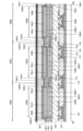
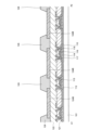
- 3 is a cross-sectional view of the display device shown in FIG. 2 taken along line A1-A2; FIG. 3 is a cross-sectional view of the display device shown in FIG. 2 taken along line B1-B2;
- FIG. 1A to 1D are cross-sectional views illustrating a method for manufacturing a display device according to an embodiment of the present invention
- 9 is an enlarged view of a part of the cross-sectional view shown in FIG. 8
- FIG. 1A to 1D are cross-sectional views illustrating a method for manufacturing a display device according to an embodiment of the present invention
- 1A to 1D are cross-sectional views illustrating a method for manufacturing a display device according to an embodiment of the present invention
- 1 is an enlarged view of a pixel layout when a display device according to an embodiment of the invention is viewed in plan
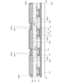
- FIG. 13 is a cross-sectional view of the display device shown in FIG. 12 taken along line A1-A2;
- FIG. 13 is a cross-sectional view of the display device shown in FIG. 12 taken along line B1-B2;
- FIG. 15 is an enlarged view of a part of the cross-sectional view shown in FIG. 14;
- FIG. 1 is an enlarged view of a pixel layout when a display device according to an embodiment of the invention is viewed in plan;
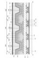
- FIG. 17 is a cross-sectional view of the display device shown in FIG. 16 taken along line A1-A2;
- FIG. It is an enlarged view of a pixel layout when the display device is viewed in plan.
- 19 is a cross-sectional view of the display device shown in FIG. 18 taken along line C1-C2;
- FIG. 19 is a cross-sectional view of the display device shown in FIG.
- FIG. 18 taken along line D1-D2;
- FIG. It is an enlarged view of a pixel layout when the display device is viewed in plan.
- 22 is a cross-sectional view of the display device shown in FIG. 21 taken along line E1-E2;
- FIG. 22 is a cross-sectional view of the display device shown in FIG. 21 taken along line F1-F2;
- FIG. 1 is a cross-sectional view of a pixel in a conventional display device;
- these films when one film is processed to form a plurality of films, these films may have different functions and roles. However, these films are derived from films formed as the same layer in the same process, and have the same layer structure and the same material. Therefore, these multiple films are defined as existing in the same layer.
- FIG. 1 A display device according to an embodiment of the present invention will be described with reference to FIGS. 1 to 11.
- FIG. 1 A display device according to an embodiment of the present invention will be described with reference to FIGS. 1 to 11.
- FIG. 1 is a schematic diagram showing the configuration of a display device 100 according to an embodiment of the present invention, showing the schematic configuration when the display device 100 is viewed from above.
- the state of viewing the display device 100 from a direction perpendicular to the screen (display area) is referred to as “planar view”.
- the display device 100 has a display area 102 formed on an insulating surface, a scanning line driving circuit 104, a driver IC 106, and a terminal section in which a plurality of terminals 107 are arranged.
- a light-emitting element having an organic layer including a light-emitting layer is arranged in the display area 102 .
- a peripheral area 103 surrounds the display area 102 .
- the driver IC 106 functions as a control section that gives signals to the scanning line driving circuit 104 and the data line driving circuit.
- the data line driving circuit may be provided with a sampling switch or the like on the substrate 101 separately from the driver IC 106 .
- the driver IC 106 is provided on the flexible printed circuit (FPC) 108 , but may be provided on the substrate 101 .
- the flexible printed circuit 108 is connected to a plurality of terminals 107 provided in the peripheral area 103 .
- the insulating surface is the surface of the substrate 101.
- the substrate 101 supports each layer provided on its surface, such as an insulating layer and a conductive layer.
- the substrate 101 itself may be made of an insulating material and have an insulating surface, or an insulating film may be separately formed on the substrate 101 to form the insulating surface.
- the material of the substrate 101 and the material forming the insulating film are not particularly limited.
- an insulating film provided above the substrate 101 can provide an insulating surface.
- a plurality of pixels 105 are arranged in a matrix in the X direction and the Y direction.
- a pixel refers to a minimum unit capable of displaying a desired color in the display area 102 .
- Each pixel 105 has a pixel circuit and a light-emitting element electrically connected to the pixel circuit.
- a light-emitting element includes a pixel electrode, an organic layer (light-emitting portion) including a light-emitting layer laminated on the pixel electrode, and a counter electrode.
- a light-emitting element included in the pixel 105 emits red, green, or blue light.
- the emission peak wavelength of the blue light-emitting element is 460 nm or more and 500 nm or less.
- the emission peak wavelength of the red light emitting element is 610 nm or more and 780 nm or less.
- the emission peak wavelength of the green light emitting element is 500 nm or more and 570 nm or less.
- the color emitted by the light-emitting element is not limited to the above, and at least one color or more may be used.
- a pixel that emits red light is denoted by a pixel 105R
- a pixel that emits green light is denoted by a pixel 105G
- a pixel that emits blue light is denoted by a pixel 105B.
- constituent elements included in the pixels 105R, 105G, and 105B are assigned R, G, and B symbols for distinction.
- the pixels 105R, 105G, and 105B are simply referred to as pixels 105 when they are not distinguished from each other. The same is true for each component of the pixels 105R, 105G, and 105B.
- the pixels 105 are electrically connected to the scanning lines 111 and the data lines 113 .
- the pixels 105 are electrically connected to a power supply line (not shown).
- the scanning lines 111 extend along the X direction and are electrically connected to the scanning line driving circuit 104 .
- the data line 113 extends along the Y direction and is electrically connected to the driver IC 106 .
- the driver IC 106 also outputs scanning signals to the scanning lines 111 via the scanning line driving circuit 104 .
- Driver IC 106 outputs a data signal corresponding to image data to data line 113 .
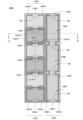
- FIG. 2 is an enlarged view of the pixel layout when the display device 100 is viewed from above
- FIG. 3 is a cross-sectional view of the pixel layout shown in FIG. 2 cut along line A1-A2.
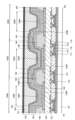
- FIG. 4 is a cross-sectional view of the pixel layout shown in FIG. 2 taken along line B1-B2.
- the configuration of a top emission display device will be described.
- FIG. 2 shows regions in which a pixel 105R having a red light emitting element, a pixel 105G having a green light emitting element, and a pixel 105B having a blue light emitting element are provided.
- the pixel 105R, pixel 105G, and pixel 105B are arranged side by side in the X direction.
- Each of the plurality of pixels 105R, the plurality of pixels 105G, and the plurality of pixels 105B is arranged in stripes along the Y direction.
- the area surrounded by short wavy lines is the area where the pixel electrode 124 is provided.
- the shape of the pixel electrode 124 in plan view is, for example, rectangular.
- a plurality of pixel electrodes 124 are arranged in a matrix in the X direction and the Y direction.
- pixel electrodes 124R, 124G, and 124B are arranged side by side in the X direction.
- the area surrounded by broken lines is the area where the organic insulating layer 126 is provided.
- the organic insulating layer 126 is also called a partition or bank.
- the shape of the organic insulating layer 126 when viewed from above is rectangular.
- the organic insulating layer 126 is arranged so as to cover the ends of the two pixel electrodes 124 adjacent in the Y direction.
- the organic insulating layer 126 is not arranged on two pixel electrodes 124 adjacent in the X direction. That is, the organic insulating layer 126 is arranged in the region where the light emitting elements of the same color are adjacent, and the organic insulating layer 126 is not arranged in the region where the light emitting elements of different colors are adjacent.
- the length of the organic insulating layer 126 in the X direction when viewed in plan is smaller than the length of the pixel electrode 124 in the X direction, but the present invention is not limited to this.
- the length of the organic insulating layer 126 in the X direction may be substantially the same as the length (width) of the pixel electrode 124 in the X direction.
- regions indicated by solid lines are regions where the light-emitting layers 132R, 132G, and 132B are provided.
- the light emitting layer 132R has light emitting layers 132R-1 to 132R-3.
- a plurality of layers formed in the same process are distinguished by numbers such as ⁇ 1, ⁇ 2, ⁇ 3, and the like. Note that when a plurality of layers formed in the same process are described without distinguishing between them, they may not be numbered.
- the light emitting layers 132R-1 to 132R-3 are separated from each other.
- the light emitting layer 132R-1 is arranged on a plurality of pixel electrodes 124R adjacent in the Y direction.
- the light emitting layer 132R-2 is arranged adjacent to the pixel electrode 124R in the X direction.
- the light emitting layer 132R-3 is arranged between the pixel electrode 124R and the pixel electrode 124G. That is, the light emitting layers 132R-1 to 132R-3 extend along the Y direction and are separated in the X direction.
- the light-emitting layer 132R has a region extending along the Y direction on the pixel electrode 124 and a region extending along the Y direction between two adjacent pixel electrodes 124 .
- the light emitting layer 132G has light emitting layers 132G-1 to 132G-3.
- the light emitting layer 132G-1 is arranged on a plurality of pixel electrodes 124G adjacent in the Y direction.
- the light emitting layer 132G-2 is arranged between the pixel electrode 124R and the pixel electrode 124G.
- the light emitting layer 132G-3 is arranged between the pixel electrode 124G and the pixel electrode 124B.
- the light emitting layers 132B-1 to 132B-3 are separated from each other.
- the light-emitting layer 132B-1 is arranged on a plurality of pixel electrodes 124B adjacent in the Y direction.
- the light emitting layer 132B-2 is arranged between the pixel electrode 124G and the pixel electrode 124B.
- the light emitting layer 132B-3 is arranged adjacent to the pixel electrode 124B in the X direction.
- the light-emitting layers 132R-3 and 132G-2 overlap each other, and the light-emitting layers 132G-3 and 132B-2 overlap each other.
- the length (width) of the light emitting layer 132R-1 in the X direction is substantially the same as the length (width) of the pixel electrode 124R in the X direction.
- the length (width) in the X direction of the light emitting layer 132G-1 is substantially the same as the length (width) in the X direction of the pixel electrode 124R.
- the length (width) in the X direction of the light emitting layer 132B-1 is substantially the same as the length (width) in the X direction of the pixel electrode 124R.
- the light-emitting layer 132 is separated into a region overlapping with the pixel electrode 124 and the organic insulating layer 126 and a region adjacent to the pixel electrode 124 .
- the length of the light-emitting layer 132R-1 in the X direction becomes substantially the same as the length of the pixel electrode 124 in the X direction.
- the region where the pixel electrode 124 and the light-emitting layer 132 overlap corresponds to the light-emitting region when the light-emitting element 130 emits light.
- FIG. 3 shows a cross-sectional view of a plurality of pixels 105B.
- a light emitting element 130B is provided in the pixel 105B.
- the light-emitting region of the light-emitting element 130 is shown as the light-emitting region 120. As shown in FIG.
- a plurality of transistors 110 are provided over the substrate 101 with an insulating film 112 interposed therebetween.
- a pixel circuit is configured by the plurality of transistors 110 .
- a transistor 110 includes at least a semiconductor layer 114 , a gate insulating film 115 , and a gate electrode 116 .
- An interlayer insulating film 121 is provided over the transistor 110 .
- Source or drain electrodes 117 and 118 are provided on the interlayer insulating film 121 .
- Each of source or drain electrodes 117 and 118 is connected to semiconductor layer 114 through a contact hole provided in interlayer insulating film 121 .
- An insulating film 122 is provided on the interlayer insulating film 121 .
- the insulating film 122 can reduce unevenness caused by the transistor 110 and the source or drain electrodes 117 and 118 .
- the plurality of transistors 110 provided over the substrate 101 and the interlayer insulating film 121 and the insulating film 122 provided over the transistors 110 are formed using known materials and methods. 4 and subsequent drawings, the configuration of the pixel circuit provided below the insulating film 122 is the same as that in FIG. 3, so detailed description thereof will be omitted.
- a plurality of pixel electrodes 124B are provided on the insulating film 122 .
- the pixel electrode 124B is electrically connected to the transistor 110 included in the pixel circuit.
- the pixel electrode 124B functions as an anode.
- a highly reflective metal film such as silver is used.
- a transparent conductive layer with a high work function such as an indium oxide-based transparent conductive layer (for example, ITO: Indium Tin Oxide) or a zinc oxide-based transparent conductive layer (for example, IZO: Indium Zinc Oxide, ZnO: Zinc Oxide) is used. may be used.
- ITO Indium Tin Oxide
- IZO Indium Zinc Oxide
- ZnO Zinc Oxide
- An organic insulating layer 126 is provided on the insulating film 122 so as to cover the ends of the pixel electrodes 124B.
- the organic insulating layer 126 is provided at the ends of the two adjacent pixel electrodes 124B.
- the organic insulating layer 126 is arranged so that the organic layer 160 including the light emitting layer 132B provided on the plurality of pixel electrodes 124B is continuously provided without being cut in the plurality of adjacent pixels 105B. be. Therefore, the organic insulating layer 126 preferably slopes gently. Also, the cross section of the upper end of the organic insulating layer 126 is preferably rounded.
- the organic insulating layer 126 can use known organic resin materials such as polyimide, polyamide, acrylic, epoxy, or siloxane. Note that the organic insulating layer 126 is not provided between the pixel electrodes 124B and 124G. Also, the organic insulating layer 126 is not provided between the pixel electrodes 124G and 124R. In other words, the organic insulating layer 126 is provided when the light emitting elements 130 of the same color are continuously arranged in the adjacent pixel electrodes 124 .
- a common layer 128 is provided on the plurality of pixel electrodes 124B and the plurality of organic insulating layers 126 .
- the common layer 128 is commonly provided over the plurality of light emitting elements 130B.
- Common layer 128 includes at least one of a hole transport layer and a hole injection layer.
- a light-emitting layer 132B is provided on the common layer 128 .
- the light emitting layer 132B-1 is commonly provided over the plurality of light emitting elements 130B.
- a common layer 134 is provided on the light emitting layer 132B-1.
- the common layer 134 is commonly provided over the plurality of light emitting elements 130B.
- Common layer 134 includes at least one of an electron transport layer and an electron injection layer.
- organic layers 160 include common layer 128 , light emitting layer 132 , and common layer 134 .
- a counter electrode 136 is provided on the common layer 134 .
- the counter electrode 136 is commonly provided over the plurality of light emitting elements 130B.
- a light-transmitting electrode is used as the counter electrode 136 .
- a MgAg thin film or a transparent conductive layer (ITO or IZO) is used as the counter electrode 136 .
- a sealing film 150 is provided on the counter electrode 136 .
- the sealing film 150 has an inorganic insulating film 151 , an organic insulating film 152 and an inorganic insulating film 153 .
- the inorganic insulating film 151 and the inorganic insulating film 153 can prevent moisture from entering the light emitting element 130 .
- the organic insulating film 152 between the inorganic insulating film 151 and the inorganic insulating film 153 cracking of the sealing film 150 can be suppressed.
- the inorganic insulating film 151 and the inorganic insulating film 153 are in contact with each other, which is preferable because the sealing function against moisture is improved.
- FIG. 4 shows a cross-sectional view of pixels 105R, 105G, and 105B.
- the pixel 105R is provided with the light emitting element 130R
- the pixel 105G is provided with the light emitting element 130G
- the pixel 105B is provided with the light emitting element 130B.
- the light emitting regions of the light emitting elements 130R, 130G and 130B are shown as light emitting regions 120R, 120G and 120B.
- Pixel electrodes 124 R, 124 G, and 124 B are provided on the insulating film 122 .
- a common layer 128 is provided on the pixel electrodes 124R, 124G, and 124B. In FIG. 4, the common layer 128 is separated by the top edges of the pixel electrodes 124R, 124G, 124B. Therefore, the common layer 128 is composed of common layers 128-1 to 128-7.
- a common layer 128-2 is provided on the pixel electrode 124R, a common layer 128-4 is provided on the pixel electrode 124G, and a common layer 128-6 is provided on the pixel electrode 124B.
- the common layer 128-1 is provided adjacent to the pixel electrode 124R in the X direction.
- the common layer 128-3 is provided between the pixel electrode 124R and the pixel electrode 124G.
- a common layer 128-5 is provided between the pixel electrode 124G and the pixel electrode 124B.
- the common layer 128-7 is provided adjacent to the pixel electrode 124B in the X direction.
- the film thickness of the pixel electrode 124 is larger than the film thickness of the common layer 128 . Therefore, when forming the common layer 128 on the pixel electrode 124 by vapor deposition, the common layer 128 is less likely to adhere to the side surfaces of the pixel electrode 124 . Thereby, the common layer 128 can be separated at the upper end portion of the pixel electrode 124 .
- the film thickness of the pixel electrode 124 is, for example, 60 nm or more and 350 nm or less.
- the thickness of the common layer 128 is, for example, in the range of 30 nm to 150 nm and less than the thickness of the pixel electrode 124 .
- the thickness of the common layer 128 may vary according to the color of light emitted by the light emitting device 130 . That is, the thickness of the common layer 128-2, the thickness of the common layer 128-4, and the thickness of the common layer 128-6 may be different. Even in this case, the thickness of the pixel electrodes 124R, 124G and 124B is preferably larger than the thickness of the common layers 128-2, 128-4 and 128-6.
- the common layer 128 includes a hole injection layer provided in contact with the pixel electrode 124 and a hole transport layer laminated thereon. At this time, if the film thickness of the hole injection layer is smaller than the film thickness of the pixel electrode 124 , the total thickness of the common layer 128 including the lamination of the hole injection layer and the hole transport layer may exceed the pixel electrode 124 .
- the common layer 128 it is desirable for the common layer 128 to be divided over the entire layer, but the hole injection layer in the common layer 128 improves the efficiency of hole injection from the pixel electrode 124 .
- the resistance can be relatively low due to the action of the dopant added for the purpose. Therefore, by dividing the layer by the upper end portion of the pixel electrode 124, the leakage current in the horizontal direction can be reduced.
- the film thickness of the pixel electrode 124 is, for example, 60 nm or more and 350 nm or less.
- the thickness of the common layer 128 is, for example, in the range of 100 nm to 150 nm and less than the thickness of the pixel electrode 124.
- the thickness of the hole injection layer provided in contact with the pixel electrode 124 is, for example, The thickness should be 10 nm or more and 30 nm or less.
- light emitting layers 132R-1 to 132R-3 On the common layer 128, light emitting layers 132R-1 to 132R-3, light emitting layers 132G-1 to 132G-3, and light emitting layers 132B-1 to 132B-3 are provided.
- Light-emitting layer 132R-1 is provided on common layer 128-2
- light-emitting layer 132G-1 is provided on common layer 128-4
- light-emitting layer 132B-1 is provided on common layer 128-6.
- Light-emitting layer 132R-2 is provided on common layer 128-1
- light-emitting layer 132R-3 and light-emitting layer 132G-2 are provided on common layer 128-3
- light-emitting layer 132G-3 and light-emitting layer 132B- 2 is provided on common layer 128-5.
- the sum of the film thickness of the pixel electrode 124 and the film thickness of the common layer 128 is larger than the film thickness of the light emitting layer 132 . Therefore, when the light-emitting layer 132 is formed on the common layer 128 by vapor deposition, the light-emitting layer 132 is less likely to adhere to the side surfaces of the pixel electrodes 124 and the common layer 128 . Thereby, the light emitting layer 132 can be separated at the upper end portion of the common layer.
- the film thickness of the light emitting layer 132 is 10 nm or more and 50 nm or less.
- the film thickness of the light emitting layer 132 may vary depending on the color of light emitted from the light emitting element 130 . Even in this case, the sum of the film thickness of the pixel electrode 124 and the film thickness of the common layer 128 is preferably larger than the film thickness of the light-emitting layer 132 .
- a common layer 134 is provided on the light-emitting layers 132R, 132G, and 132B. Common layer 134 is separated by light emitting layers 132R-1, 132G-1, 132B-1. Therefore, the common layer 134 is composed of common layers 134-1 to 134-7.
- a common layer 134-2 is provided on the light-emitting layer 132R-1
- a common layer 134-4 is provided on the light-emitting layer 132G-1
- a common layer 134-6 is provided on the light-emitting layer 132B-1. is provided.
- the common layer 134-1 is provided adjacent to the pixel electrode 124R. Also, the common layer 134-3 is provided between the pixel electrode 124R and the pixel electrode 124G.
- a common layer 134-5 is provided between the pixel electrode 124G and the pixel electrode 124B.
- the common layer 134-7 is provided adjacent to the pixel electrode 124B in the X direction.
- a counter electrode 136 is provided on the common layer 134 .
- the counter electrodes 136 are separated by common layers 134-2, 134-4, 134-6. Therefore, the counter electrode 136 is composed of counter electrodes 136-1 to 136-7.
- a counter electrode 136-2 is provided on the common layer 134-2
- a counter electrode 136-4 is provided on the common layer 134-4
- a counter electrode 136-6 is provided on the common layer 134-6.
- the counter electrode 136-1 is provided adjacent to the pixel electrode 124R.
- the counter electrode 136-3 is provided between the pixel electrode 124R and the pixel electrode 124G.
- the counter electrode 136-5 is provided between the pixel electrode 124G and the pixel electrode 124B.
- the counter electrode 136-7 is provided adjacent to the pixel electrode 124B in the X direction.
- FIG. 24 omits the illustration of the configuration of the pixel circuit provided below the insulating film 222 .
- FIG. 24 shows a cross-sectional view of pixels 205R, 205G, and 205B in a conventional display device.
- the pixel 205R is provided with the light emitting element 230R
- the pixel 205G is provided with the light emitting element 230G
- the pixel 205B is provided with the light emitting element 230B.
- the light-emitting element 230R has at least a pixel electrode 224R, a light-emitting layer 232R, and a counter electrode 236.
- the light emitting element 230G has at least a pixel electrode 224G, a light emitting layer 232G, and a counter electrode 236. As shown in FIG.
- the light-emitting element 230B has at least a pixel electrode 224B, a light-emitting layer 232B, and a counter electrode 236.
- FIG. A common layer 228 is provided between the pixel electrodes 224R, 224G, 224B and the light emitting layers 232R, 232G, 232B.
- a common layer 234 is provided between the light emitting layers 232R, 232G, 232B and the counter electrode 236. As shown in FIG. The common layers 228 and 234 are commonly provided over the light emitting elements 230R, 230G and 230B (over the display area). In FIG.
- the pixel electrodes 224R, 224G, 224B are anodes and the counter electrode 236 is a cathode.
- common layer 228 includes at least one of a hole transport layer and a hole injection layer
- common layer 234 includes at least one of an electron transport layer and an electron injection layer.
- the ends of the pixel electrodes 224R, 224G, and 224B are covered with an insulating layer 226. Further, openings 220R, 220G and 220B are provided in the insulating layer 226 so as to expose the pixel electrodes 224R, 224G and 224B. The openings 220R, 220G, and 220B correspond to light emitting regions in the light emitting element.
- a light-emitting layer 232B and a light-emitting layer 232R are provided on the common layer 228 on the insulating layer 226 . Part of the light emitting layer 232B overlaps part of the light emitting layer 232R.
- the light emission start voltage of the light emitting layer 232B is higher than the light emission start voltages of the light emitting layers 228R and 232G. Therefore, when the light-emitting element 230B emits light, a large voltage is applied to the light-emitting layer 232B, and holes in the common layer 228 laterally move from the pixel 205B toward the pixels 205R and 205G.
- the light-emitting layer 232B When the light-emitting layer 232B exhibits hole-transport properties, holes pass through the light-emitting layer 232B in the thickness direction. Therefore, the light emitting layer 232R and the light emitting layer 232G emit light at the end of the light emitting layer 232R. Alternatively, when the light-emitting layer 232B exhibits an electron-transport property, holes do not pass through the thickness direction of the light-emitting layer 232B, but move laterally. Therefore, the light emitting layer 232R emits light near the edge of the light emitting layer 232B.
- the light emission start voltage of the light emitting layer 232R and the light emission start voltage of the light emitting layer 232G are approximately the same.
- lateral leakage current may cause adjacent pixels to emit light, degrading the display characteristics of the EL display device.
- the regions provided with the light-emitting layers 232 may be formed apart from each other so as not to overlap each other.
- the openings 220R, 220G, and 220B must be formed sufficiently apart from each other, and the definition is reduced. There is a problem of lowering.
- the common layer 128 is separated so as to extend in the Y direction. Specifically, the common layer 128 is separated by utilizing the coverage of the organic material at the edge of the pixel electrode 124 . This separates the common layer 128 between the different color pixels 105R, 105G, 105B. Therefore, lateral leakage current can be suppressed from flowing through the common layer 128 . Accordingly, it is possible to suppress unintended light emission between the pixels 105R, 105G, and 105B of different colors, so that the display characteristics of the EL display device can be improved.
- the region where the light emitting element emits light is limited to the region where the pixel electrode 124 is provided, so that unintended light emission can be further suppressed.
- the common layers 128 and 134 and the counter electrode 136 also extend along the Y direction and are separated in the X direction, similarly to the light emitting layer 132 . That is, the common layers 128 and 134 and the counter electrode 136 are divided into regions extending along the Y direction on the pixel electrodes 124 adjacent to each other in the Y direction and regions extending in the Y direction between two pixel electrodes 124 adjacent to each other in the X direction. and a region extending along.
- the organic layer 160 and the counter electrode 136 may be connected to each other in regions extending along the Y direction in the peripheral region 103 .
- the common layers 128-1 to 128-7 may be separated from each other in regions extending along the Y direction in the display region 102, and may extend along the Y direction in the peripheral region 103. regions may be connected to each other.
- the counter electrodes 136-1 to 136-7 may be separated from each other in regions extending along the Y direction in the display region 102, and may extend along the Y direction in the peripheral region 103. regions may be connected to each other.
- the common layer 128 that causes the lateral leakage current to flow. Therefore, at least the common layers 128 need only extend along the Y direction and be separated in the X direction.
- the common layer 134 and the counter electrode 136 may be provided continuously over the entire display area 102 . If at least the common layers 128 extend along the Y direction and are separated in the X direction, it is possible to suppress lateral leakage current from flowing through the common layers 128 .
- FIG. 5 to 11 the manufacturing method of the configuration corresponding to the cross-sectional view taken along the line B1-B2 shown in FIG. 2 will be described unless otherwise specified.
- a transistor 110 forming a pixel circuit is provided on a substrate 101.
- An interlayer insulating film 121 containing at least one of silicon oxide and silicon nitride is formed over the transistor 110 .
- Source or drain electrodes 117 and 118 are formed on the interlayer insulating film 121 .
- An insulating film 122 is formed on the interlayer insulating film 121 .
- the insulating film 122 functions as a planarizing film.
- the insulating film 122 is composed of an organic resin material.
- organic resin material known organic resin materials such as polyimide, polyamide, acrylic, epoxy, or siloxane can be used.
- the insulating film 122 By providing the insulating film 122 over the transistor 110 or the interlayer insulating film 121, unevenness of the transistor can be reduced.
- Contact holes are formed in the insulating film 122 to partially expose the source or drain electrodes 117 and 118 . The contact hole is for connecting the pixel electrode 124 to be formed in the next step and the source or drain electrode 117 .
- FIG. 5 is a diagram for explaining the steps of forming the insulating film 122 and the pixel electrodes 124R, 124G, and 124B.
- the pixel electrodes 124R, 124G, and 124B are formed by vapor deposition using metal masks. Each of the pixel electrodes 124 R, 124 G, and 124 B is electrically connected to the source or drain electrode 117 connected to the transistor 110 through contact holes provided in the insulating film 122 .
- the pixel electrodes 124R, 124G, and 124B function as anodes.
- the film thickness of the pixel electrode 124 is preferably, for example, 60 nm or more and 350 nm or less.
- the pixel electrodes 124R, 124G, and 124B are formed with a three-layer structure of lower ITO, Ag, and upper ITO layers will be described.
- the thickness of the lower layer ITO is 5 nm or more and 100 nm or less
- the thickness of Ag is 50 nm or more and 200 nm or less
- the thickness of the upper layer ITO is 5 nm or more and 50 nm or less.
- FIG. 6 is a diagram for explaining the process of forming a plurality of organic insulating layers 126.
- FIG. 6 corresponds to a cross-sectional view taken along line A1-A2 shown in FIG.
- an organic insulating layer 126 is provided between pixel electrodes 124 adjacent in the Y direction.
- the organic insulating layer 126 is provided so as to cover the edges of the adjacent pixel electrodes 124 .
- the organic insulating layer 126 is composed of an organic resin material.
- the organic insulating layer 126 is not formed between the pixel electrodes 124R and 124G, between the pixel electrodes 124G and 124B, and between the pixel electrodes 124B and 124R.
- organic resin material known organic resin materials such as polyimide, polyamide, acrylic, epoxy, or siloxane can be used.
- FIG. 7 is a diagram for explaining the steps of forming the common layer 128 and the light emitting layer 132R.
- Common layers 128-1 to 128-7 are formed on the pixel electrodes 124R, 124G and 124B.
- Common layers 128-1 to 128-7 include at least one of a hole transport layer and a hole injection layer. Known materials may be appropriately used for the hole transport layer and the hole injection layer.
- the common layer 128 is formed on the pixel electrode 124 by vapor deposition, the common layer 128 overhangs when the common layer 128 is deposited on the pixel electrode 124 .
- the common layer 128 is less likely to adhere to the side surface of the pixel electrode 124, and the common layer 128 is more likely to break. Thereby, the common layer 128 can be separated at the upper end portion of the pixel electrode 124 .
- FIG. 8 is a plan view after forming the common layer 128.
- the common layers 128-1 to 128-7 are each separated in the X direction. Also, the common layers 128-1 to 128-7 each extend in the Y direction.
- the common layers 128-2, 128-4, 128-6 overlap the pixel electrodes 124 and the organic insulating layer 126.
- FIG. The common layers 128-1, 128-3, 128-5, 128-7 do not overlap the pixel electrodes 124.
- a light emitting layer 132R is formed on the common layers 128-1 to 128-3.
- the light-emitting layer 132R overhangs when the light-emitting layer 132R is deposited on the common layer 128-2. Since the overhanging portion has an eaves structure, the light emitting layer 132R is less likely to stick to the side surfaces of the common layer 28-2 and the pixel electrode 124R, and the light emitting layer 132R is more likely to be disconnected. Thereby, the light emitting layer 132R can be separated at the upper end portion of the common layer 128-2. Thus, light emitting layers 132R-1 to 132R-3 are formed.
- FIG. 9 is an enlarged view of the area 170 shown in FIG. 9, the pixel electrode 124 has a three-layer structure of a transparent conductive layer 141, a metal layer 142, and a transparent conductive layer 143.
- the transparent conductive layers 141 and 143 may protrude beyond the edge of the metal layer 142 . Since the end portion of the transparent conductive layer 143 has a canopy structure, the common layer 128 is less likely to stick to the side surface of the pixel electrode 124, and the common layer 128 is more likely to be cut off.
- the common layer 128 can be separated at the end of the transparent conductive layer 143 .
- the step disconnection of the common layer 128 can be reliably performed at the upper end portion of the pixel electrode 124 .
- the light-emitting layer 132R is formed on the common layer 128, the light-emitting layer 132R can be reliably cut off at the upper end of the common layer 128-2.
- FIG. 10 is a diagram explaining the process of forming the light emitting layers 132G and 132B.
- the method for forming the light emitting layers 132G and 132B is the same as the method for forming the light emitting layer 132R.
- a light-emitting layer 132G is formed on the common layers 128-3 to 128-5 by vapor deposition.
- the light emitting layers 132G-1 to 132G-3 are formed by separating the light emitting layer 132G at the ends of the common layer 128-4.
- a light-emitting layer 132B is formed on the common layers 128-5 to 128-7 by vapor deposition.
- the light emitting layers 132B-1 to 132B-3 are formed by separating the light emitting layer 132B at the ends of the common layer 128-6.
- FIG. 11A and 11B are diagrams for explaining the steps of forming the common layer 134 and the counter electrode 136.
- FIG. Common layers 134-1 to 134-7 are formed on the light emitting layers 132R, 132G, and 132B.
- Common layers 134-1 to 134-7 include at least one of an electron transport layer and an electron injection layer. Known materials may be appropriately used for the electron-transporting layer and the electron-injecting layer.
- the common layer 134 is formed on the light-emitting layers 132R, 132G, and 132B by vapor deposition, the common layer 134 is separated at the ends of the light-emitting layers 132R-1, 132G-1, and 132B-1.
- Common layers 134-1 to 134-7 are thus formed. Note that the plan view after the formation of the common layer 134 is the same as FIG. 8, so the illustration is omitted.
- a counter electrode 136 is formed on the common layer 134 .
- a light-transmitting material may be used as appropriate for the counter electrode 137 .
- the counter electrodes 136 are formed on the common layer 134, the counter electrodes 136-1 to 136- are separated at the ends of the common layers 134-2, 134-4, and 134-6. 7 is formed.
- the plan view after forming the counter electrode 136 is the same as FIG. 8, so the illustration is omitted.
- a sealing film 150 is formed on the counter electrode 136 .
- the sealing film 150 is formed of an inorganic insulating film 151, an organic insulating film 152, and an inorganic insulating film 153 in this order. It is preferable that the inorganic insulating film 151 is not separated on the counter electrode 136 .
- the film thickness of the inorganic insulating film 151 is preferably a film thickness that alleviates unevenness formed by the light emitting element 130 .
- the inorganic insulating film 151 may be thicker than the inorganic insulating film 153 .
- the display device 100 shown in FIGS. 2 to 4 can be manufactured.
- the pixels 105R, 105G, and 105B emitting light of different colors are formed by separating the common layer 128, and a plurality of pixels emitting light of the same color are formed.
- a common layer 128 is formed continuously.
- the present invention is not limited to this. There is no limitation on the formation order of the light emitting layers 132R, 132G, and 132B.
- FIGS. 2 and 8 show views in which common layers 128-1 and 128-2 are separated from each other, and common layers 128-2 and 128-3 are separated from each other.
- the common layer 128-2 may be connected to the common layer 128-1 or the common layer 128-3 in a region adjacent to the organic insulating layer 126.
- FIG. Since the side surfaces of the organic insulating layer 126 have a gentle slope, the common layers 128-1, 128-2, and 128-3 may not be separated in the regions adjacent to the organic insulating layer 126.
- FIG. 12 is a plan view of a display device 100A according to one embodiment of the invention.
- the planar layout of the organic layer 160 including the light-emitting layer 132 is the same as in FIGS. 2 and 8, so the illustration is omitted.
- an inorganic insulating layer 138 is provided on the pixel electrodes 124R, 124G, 124B and the organic insulating layer 126. As shown in FIG. The inorganic insulating layer 138 is provided so as to cover peripheral portions of the pixel electrodes 124R, 124G, and 124B. In other words, the inorganic insulating layer 138 is provided with an opening so as to expose the surface of the pixel electrode 124R. The inorganic insulating layer 138 is provided so as to overlap with the organic insulating layer 126 .
- the inorganic insulating layer 138 is made of, for example, a silicon nitride film. The film thickness of the inorganic insulating layer 138 is, for example, 50 nm or more and 500 nm or less.
- FIG. 13 is a cross-sectional view taken along line A1-A2 shown in FIG.
- inorganic insulating layer 138 covers organic insulating layer 126 . Therefore, the organic layer 160 is provided on the pixel electrode 124 and the inorganic insulating layer 138 .
- the pixel electrode 124 and the common layer 128 are in contact with each other at the opening of the inorganic insulating layer 138 .
- the opening of the inorganic insulating layer 138 becomes the light emitting region of the light emitting element 130 .
- FIG. 14 is a cross-sectional view taken along line B1-B2 shown in FIG.
- the inorganic insulating layer 138 covers peripheral portions of the pixel electrodes 124R, 124G, and 124B.
- a common layer 128 is provided on the pixel electrodes 124R, 124G, 124B and the inorganic insulating layer 138.
- the film thickness of the pixel electrode 124 is greater than the film thickness of the common layer 128 .
- An inorganic insulating layer 138 is provided on the side surface of the pixel electrode 124 .
- FIG. 15 is an enlarged view of the area 170A shown in FIG.
- the pixel electrode 124 has a three-layer structure of a transparent conductive layer 141 , a metal layer 142 and a transparent conductive layer 143 .
- the transparent conductive layers 141 and 143 may protrude beyond the edge of the metal layer 142 .
- the inorganic insulating layer 138 is formed by sputtering, for example.
- the inorganic insulating layer 138 is also formed on the side surfaces of the transparent conductive layer 141 , the metal layer 142 and the transparent conductive layer 143 .
- the film thickness of the inorganic insulating layer 138 is added to the film thickness of the pixel electrode 124 . Therefore, when the common layer 128 is formed on the pixel electrode 124 and the inorganic insulating layer 138 by vapor deposition, the ends of the inorganic insulating layer 138 are more likely to protrude.
- the common layer 128 is less likely to adhere to the side surface of the inorganic insulating layer 138, and the common layer 128 is more likely to be cut off. Thereby, the common layer 128 can be separated at the upper end portion of the pixel electrode 124 .
- the inorganic insulating layer 138 covers the side surfaces of the pixel electrodes 124 . This can prevent electrical connection between the pixel electrode 124 and the organic layer 160 provided between two adjacent pixel electrodes 124 .
- FIG. 16 is a plan view of a display device 100B according to one embodiment of the invention.
- the planar layout of the organic layer 160 including the light-emitting layer 132 is the same as in FIGS. 2 and 8, so the illustration is omitted.
- the stacking order of the organic insulating layer 126 and the inorganic insulating layer 138 is different.
- the inorganic insulating layer 138 is provided on the pixel electrodes 124R, 124G and 124B. Also, the organic insulating layer 126 is provided on the pixel electrodes 124R, 124G, 124B and the inorganic insulating layer 138.
- FIG. The inorganic insulating layer 138 is provided so as to cover peripheral portions of the pixel electrodes 124R, 124G, and 124B. In other words, the inorganic insulating layer 138 is provided with an opening so as to expose the surface of the pixel electrode 124R.
- the inorganic insulating layer 138 is provided so as to overlap with the organic insulating layer 126 .
- the inorganic insulating layer 138 is made of, for example, a silicon nitride film. The film thickness of the inorganic insulating layer 138 is, for example, 50 nm or more and 500 nm or less.
- FIG. 17 is a cross-sectional view taken along line A1-A2 shown in FIG.
- the inorganic insulating layer 138 covers peripheral portions of the pixel electrodes 124R, 124G, and 124B.
- a common layer 128 is provided on the pixel electrodes 124 R, 124 G, 124 B and the organic insulating layer 126 .
- a cross-sectional view taken along line B1-B2 shown in FIG. 16 is similar to FIG. 14, so detailed description thereof will be omitted.
- the inorganic insulating layer 138 covers the side surfaces of the pixel electrodes 124 . This can prevent electrical connection between the pixel electrode 124 and the organic layer 160 provided between two adjacent pixel electrodes 124 .
- FIG. 18 is an enlarged view of the pixel layout when the display device 100C is viewed from above, and FIG. 19 is a cross-sectional view of the pixel layout shown in FIG. 18 cut along line C1-C2.
- FIG. 20 is a cross-sectional view of the pixel layout shown in FIG. 18 taken along line D1-D2.
- pixels 105R and pixels 105G are alternately arranged in the Y direction.
- the pixels 105B are arranged side by side in the Y direction.
- the pixel 105R is arranged adjacent to the pixel 105B in the X direction.
- the pixel 105G is arranged adjacent to the pixel 105B in the X direction.
- the organic insulating layer 126 is arranged so as to cover the edge of the pixel electrode 124R and the edge of the pixel electrode 124G that are adjacent in the Y direction. Also, the organic insulating layer 126 is arranged so as to cover the end portions of the two pixel electrodes 124B adjacent in the Y direction and the end portions of the pixel electrodes 124B. The organic insulating layer 126 is not arranged between the two pixel electrodes 124R and 124B that are adjacent in the X direction. Also, the organic insulating layer 126 is not arranged between the two pixel electrodes 124G and the pixel electrode 124B that are adjacent in the X direction.
- the light emitting layer 132R has light emitting layers 132R-1 to 132R-3. Each of the light emitting layers 132R-1 to 132R-3 is separated. A light-emitting layer 132R-1 is disposed on the pixel electrode 124R. The light emitting layer 132R-2 is arranged adjacent to the pixel electrode 124R. The light emitting layer 132R-3 is arranged between the pixel electrode 124R and the pixel electrode 124B. The light emitting layer 132G has light emitting layers 132G-1 to 132G-3. A light-emitting layer 132G-1 is disposed on the pixel electrode 124G. The light emitting layer 132G-2 is arranged adjacent to the pixel electrode 124G.
- the light emitting layer 132G-3 is arranged between the pixel electrode 124G and the pixel electrode 124B.
- the light emitting layers 132B-1 to 132B-3 are separated from each other.
- the light-emitting layer 132B-1 is arranged on a plurality of pixel electrodes 124B adjacent in the Y direction.
- the light emitting layer 132B-2 is arranged between the pixel electrodes 124R, 124G and the pixel electrode 124B.
- the light emitting layer 132B-3 is arranged adjacent to the pixel electrode 124B. Although not shown, the light emitting layers 132R-2 and 132G-3 overlap the light emitting layer 132B-3.
- the light-emitting layers 132R-3 and 132G-3 overlap with the light-emitting layer 132B-2. Also, the light-emitting layer 132R-1 overlaps the light-emitting layer 132G-1 on the organic insulating layer 126. FIG.
- FIG. 19 the cross-sectional view when the pixel 105G and the pixel 105B are adjacent to each other is substantially the same as FIG. 14, so for detailed description, refer to the description regarding FIG.
- FIG. 20 shows the case where the pixel 105R and the pixel 105G are adjacent to each other.
- the light-emitting layer 132R-1 and the light-emitting layer 132G-1 overlap each other on the organic insulating layer 126.
- FIG. 20 shows the case where the pixel 105R and the pixel 105G are adjacent to each other.
- the light-emitting layer 132R-1 and the light-emitting layer 132G-1 overlap each other on the organic insulating layer 126.
- the light emitting element 130B has a higher light emission start voltage than the light emitting elements 130R and 130G. Therefore, in a region where the light emitting element 130B and the light emitting elements 130R and 130G are adjacent to each other, the voltage of the light emitting element 130B may cause unintended light emission of the light emitting elements 130R and 130G.
- the light emitting layer 132 is separated at the edge of the pixel electrode 124 . Therefore, the overlapping regions of the light emitting layer 132B and the light emitting layers 132R and 132G are less susceptible to the voltage applied to the pixel electrode 124. FIG. Therefore, it is possible to suppress the flow of the lateral leak current, so that the display quality can be improved.
- the light emission start voltage of the light emitting element 130R and the light emission start voltage of the light emitting element 130G are approximately the same. Therefore, even if either the light emitting element 130R or the light emitting element 130G emits light, the influence of the lateral leakage current from the light emitting layer 132R-1 or the light emitting layer 132G-1 is small. Therefore, on the organic insulating layer 126, there may be a region where the light emitting layer 132R-1 and the light emitting layer 132G-1 overlap each other.
- a display device 100D obtained by reversing the stacking order of the pixel electrode 124 and the counter electrode 136 in the display devices 100, 100A to 100C according to the previous embodiments will be described with reference to FIGS.
- FIG. 21 is an enlarged view of the pixel layout when the display device 100 is viewed from above
- FIG. 22 is a cross-sectional view of the pixel layout shown in FIG. 21 taken along line E1-E2.
- FIG. 23 is a cross-sectional view of the pixel layout shown in FIG. 21 taken along line F1-F2.
- the display device 100D differs from the display device 100 in that the pixel electrodes 124R, 124G, and 124B function as cathodes, and the counter electrode 136 functions as an anode.
- regions surrounded by short wavy lines are regions where the pixel electrodes 136R, 136G, and 136B are provided.
- the material of the counter electrode 136 described in the first embodiment may be used.
- the material of the pixel electrode 124 described in the first embodiment may be used.
- the pixel electrodes 124R, 124G, and 124B are each electrically connected to the transistor 110 included in the pixel circuit.
- the common layer 134 provided between the pixel electrodes 124R, 124G, 124B and the light emitting layers 132R, 132G, 132B includes at least one of an electron transport layer and an electron injection layer.
- a common layer 128 provided between the counter electrode 136 and the light emitting layers 132R, 132G, and 132B includes at least one of a hole transport layer and a hole injection layer.
- Pixel electrodes 124 R, 124 G, and 124 B are provided on the insulating film 122 .
- a common layer 134 is provided on the pixel electrodes 124R, 124G, and 124B. In FIG. 22, the common layer 134 is separated by the top edges of the pixel electrodes 124R, 136G, 136B. Therefore, the common layer 134 is composed of common layers 134-1 to 134-7.
- a common layer 134-2 is provided on the pixel electrode 124R, a common layer 134-4 is provided on the pixel electrode 124G, and a common layer 134-6 is provided on the pixel electrode 124B.
- the common layer 134-1 is provided adjacent to the pixel electrode 124R in the X direction.
- the common layer 134-3 is provided between the pixel electrode 124R and the pixel electrode 124G.
- a common layer 134-5 is provided between the pixel electrode 124G and the pixel electrode 124B.
- the common layer 134-7 is provided adjacent to the pixel electrode 124B in the X direction.
- the film thickness of the pixel electrode 124 is larger than the film thickness of the common layer 134 . Therefore, when forming the common layer 134 on the pixel electrode 124 by vapor deposition, the common layer 134 is less likely to adhere to the side surfaces of the pixel electrode 124 . Thereby, the common layer 134 can be separated at the upper end portion of the pixel electrode 124 .
- the film thickness of the pixel electrode 124 is, for example, 60 nm or more and 350 nm or less.
- the thickness of the common layer 134 is, for example, in the range of 30 nm to 150 nm and less than the thickness of the pixel electrode 124 .
- the light-emitting layers 132R, 132G, 132B are separated by upper ends of common layers 134-2, 134-4, 134-6, respectively.
- the light-emitting layer 132R has light-emitting layers 132R-1 to 132R-3
- the light-emitting layer 132G has light-emitting layers 132G-1 to 132G-3
- the light-emitting layer 132B has light-emitting layers 132B-1 to 132B-3.
- Common layer 128 is separated by the tops of light emitting layers 132R-1, 132G-1, 132B-1, respectively.
- Common layer 128 has common layers 128-1 through 128-7.
- the counter electrodes 136 are separated by upper edges of common layers 128-2, 128-4, 128-6, respectively.
- the counter electrode 136 has counter electrodes 136-1 to 124-6.
- the light emitting element 130 uses the pixel electrode 124 as a cathode and the counter electrode 136 as an anode. Even in this case, at least the common layer 134 is separated so as to extend in the Y direction between the pixels 105R, 105G, and 105B of different colors. Specifically, the common layer 134 is separated by utilizing the coverage of the organic material at the edge of the pixel electrode 124 . This separates the common layer 134 between the different color pixels 105R, 105G, 105B. Therefore, lateral leakage current can be suppressed from flowing through the common layer 134 . Accordingly, it is possible to suppress unintended light emission between the pixels 105R, 105G, and 105B of different colors, so that the display characteristics of the EL display device can be improved.
- the common layer 134 includes an electron injection layer provided in contact with the pixel electrode 124 and an electron transport layer laminated thereon. At this time, if the thickness of the electron injection layer is smaller than the thickness of the pixel electrode 124 , the total thickness of the common layer 134 including the lamination of the electron injection layer and the electron transport layer may exceed the thickness of the pixel electrode 124 . Of course, as mentioned above, it is desirable for the common layer 134 to be divided over the entire layer.
- the layer is divided by the upper end portion of the pixel electrode 128, whereby lateral leakage current can be reduced.
- the film thickness of the pixel electrode 124 is, for example, 60 nm or more and 350 nm or less.
- the thickness of the common layer 128 is, for example, in the range of 100 nm to 150 nm and less than the thickness of the pixel electrode 124.
- the thickness of the electron injection layer provided in contact with the pixel electrode 124 is, for example, The thickness should be 0.1 nm or more and 10 nm or less.
- the configuration of the display device 100D according to this embodiment can be applied to the configurations of the display devices 100 and 100A to 100C according to the previous embodiments. That is, in the display devices 100, 100A to 100C, the pixel electrode 124 may be used as the cathode and the counter electrode 136 may be used as the anode.
- the common layer 134 provided between the pixel electrode 124 and the light emitting layer 132 should include at least one of an electron transport layer and an electron injection layer.
- the common layer 128 provided between the counter electrode 136 and the light emitting layer 132 may include at least one of a hole transport layer and a hole injection layer.
- the display device according to one embodiment of the present invention can be applied to various forms. Therefore, based on the display devices 100 and 100A to 100D described as the embodiments and modifications of the invention, those skilled in the art may appropriately add, delete, or change the design of components, or add, omit, or modify processes. Modified conditions are also included in the scope of the present invention as long as they are provided with the gist of the present invention. Moreover, each embodiment described above can be combined with each other as long as there is no technical contradiction.
- the structure for suppressing leakage current in the organic layer 160 in a display device having an organic EL element as a display element has been mainly described.
- An embodiment of the present invention can be applied not only to a display device but also to a photosensor device or the like configured by arranging organic photodiodes in which an organic layer is sandwiched between electrodes in a matrix. Specifically, it can be applied to the overlapping relationship at the end of the organic layers forming the organic photodiode which are separately formed.
- 100, 100A to 100C display device, 101: substrate, 102: display area, 103: peripheral area, 104: scanning line driving circuit, 105: pixel, 105B: pixel, 105G: pixel, 105R: pixel, 106: driver IC , 107: terminal, 108: flexible printed circuit, 110: transistor, 111: scanning line, 112: insulating film, 113: data line, 114: semiconductor layer, 115: gate insulating film, 116: gate electrode, 117: source electrode or drain electrode, 118: source electrode or drain electrode, 121: interlayer insulating film, 122: insulating film, 124, 124B, 124G, 124R: pixel electrode, 126: organic insulating layer, 128, 128-1 to 128-7: Common layer 130: Light emitting element 130B: Light emitting element 130G: Light emitting element 130R: Light emitting element 132: Light emitting layer 132B, 132B-1 to 132B-3: Light emitting layer
Landscapes
- Physics & Mathematics (AREA)
- Engineering & Computer Science (AREA)
- Optics & Photonics (AREA)
- Microelectronics & Electronic Packaging (AREA)
- Manufacturing & Machinery (AREA)
- General Physics & Mathematics (AREA)
- Theoretical Computer Science (AREA)
- Electroluminescent Light Sources (AREA)
Priority Applications (3)
| Application Number | Priority Date | Filing Date | Title |
|---|---|---|---|
| CN202280082478.6A CN118383100A (zh) | 2021-12-24 | 2022-11-21 | 显示装置 |
| JP2023569184A JPWO2023119995A1 (https=) | 2021-12-24 | 2022-11-21 | |
| US18/751,946 US20240349543A1 (en) | 2021-12-24 | 2024-06-24 | Display device |
Applications Claiming Priority (2)
| Application Number | Priority Date | Filing Date | Title |
|---|---|---|---|
| JP2021-211107 | 2021-12-24 | ||
| JP2021211107 | 2021-12-24 |
Related Child Applications (1)
| Application Number | Title | Priority Date | Filing Date |
|---|---|---|---|
| US18/751,946 Continuation US20240349543A1 (en) | 2021-12-24 | 2024-06-24 | Display device |
Publications (1)
| Publication Number | Publication Date |
|---|---|
| WO2023119995A1 true WO2023119995A1 (ja) | 2023-06-29 |
Family
ID=86902233
Family Applications (1)
| Application Number | Title | Priority Date | Filing Date |
|---|---|---|---|
| PCT/JP2022/043032 Ceased WO2023119995A1 (ja) | 2021-12-24 | 2022-11-21 | 表示装置 |
Country Status (4)
| Country | Link |
|---|---|
| US (1) | US20240349543A1 (https=) |
| JP (1) | JPWO2023119995A1 (https=) |
| CN (1) | CN118383100A (https=) |
| WO (1) | WO2023119995A1 (https=) |
Citations (8)
| Publication number | Priority date | Publication date | Assignee | Title |
|---|---|---|---|---|
| JP2011065837A (ja) * | 2009-09-16 | 2011-03-31 | Sharp Corp | 有機el表示装置及びその製造方法 |
| WO2013179873A1 (ja) * | 2012-06-01 | 2013-12-05 | ソニー株式会社 | 有機電界発光装置およびその製造方法ならびに電子機器 |
| JP2014232631A (ja) * | 2013-05-29 | 2014-12-11 | ソニー株式会社 | 表示装置および表示装置の製造方法ならびに電子機器 |
| JP2016045979A (ja) * | 2014-08-19 | 2016-04-04 | ソニー株式会社 | 表示装置および電子機器 |
| US20160225834A1 (en) * | 2015-01-30 | 2016-08-04 | Samsung Display Co., Ltd. | Organic light-emitting display apparatus |
| JP2018081903A (ja) * | 2016-11-15 | 2018-05-24 | 三星ディスプレイ株式會社Samsung Display Co.,Ltd. | 有機発光表示装置及びその製造方法 |
| JP2019032939A (ja) * | 2017-08-04 | 2019-02-28 | キヤノン株式会社 | 表示装置およびその製造方法ならびに電子機器 |
| JP2020520056A (ja) * | 2017-05-17 | 2020-07-02 | アップル インコーポレイテッドApple Inc. | 横方向の漏れを低減した有機発光ダイオードディスプレイ |
-
2022
- 2022-11-21 WO PCT/JP2022/043032 patent/WO2023119995A1/ja not_active Ceased
- 2022-11-21 JP JP2023569184A patent/JPWO2023119995A1/ja active Pending
- 2022-11-21 CN CN202280082478.6A patent/CN118383100A/zh active Pending
-
2024
- 2024-06-24 US US18/751,946 patent/US20240349543A1/en active Pending
Patent Citations (8)
| Publication number | Priority date | Publication date | Assignee | Title |
|---|---|---|---|---|
| JP2011065837A (ja) * | 2009-09-16 | 2011-03-31 | Sharp Corp | 有機el表示装置及びその製造方法 |
| WO2013179873A1 (ja) * | 2012-06-01 | 2013-12-05 | ソニー株式会社 | 有機電界発光装置およびその製造方法ならびに電子機器 |
| JP2014232631A (ja) * | 2013-05-29 | 2014-12-11 | ソニー株式会社 | 表示装置および表示装置の製造方法ならびに電子機器 |
| JP2016045979A (ja) * | 2014-08-19 | 2016-04-04 | ソニー株式会社 | 表示装置および電子機器 |
| US20160225834A1 (en) * | 2015-01-30 | 2016-08-04 | Samsung Display Co., Ltd. | Organic light-emitting display apparatus |
| JP2018081903A (ja) * | 2016-11-15 | 2018-05-24 | 三星ディスプレイ株式會社Samsung Display Co.,Ltd. | 有機発光表示装置及びその製造方法 |
| JP2020520056A (ja) * | 2017-05-17 | 2020-07-02 | アップル インコーポレイテッドApple Inc. | 横方向の漏れを低減した有機発光ダイオードディスプレイ |
| JP2019032939A (ja) * | 2017-08-04 | 2019-02-28 | キヤノン株式会社 | 表示装置およびその製造方法ならびに電子機器 |
Also Published As
| Publication number | Publication date |
|---|---|
| US20240349543A1 (en) | 2024-10-17 |
| CN118383100A (zh) | 2024-07-23 |
| JPWO2023119995A1 (https=) | 2023-06-29 |
Similar Documents
| Publication | Publication Date | Title |
|---|---|---|
| TWI575731B (zh) | Display device and manufacturing method thereof | |
| KR102248641B1 (ko) | 유기전계 발광소자 | |
| CN114765208A (zh) | 显示装置 | |
| KR20190063502A (ko) | 표시패널 및 그 제조방법 | |
| US20260114132A1 (en) | Display device and manufacturing method of display device | |
| KR101890469B1 (ko) | 표시장치 및 그 제조 방법 | |
| US12185590B2 (en) | Display device including an organic layer | |
| US12426489B2 (en) | Method of manufacturing display device | |
| US12538664B2 (en) | Display device | |
| JP2019106331A (ja) | 有機el表示装置 | |
| KR20230026775A (ko) | 표시 장치 | |
| US20140097745A1 (en) | Organic EL Device | |
| KR20230064452A (ko) | 표시 장치 | |
| US20260123191A1 (en) | Display device including rib and multi-portion partition | |
| CN111819908B (zh) | 有机el显示装置 | |
| US20230389369A1 (en) | Display device | |
| WO2023119995A1 (ja) | 表示装置 | |
| US20230389393A1 (en) | Display device | |
| US12471437B2 (en) | Display device | |
| JP4300195B2 (ja) | 平板表示装置および有機電界発光表示装置 | |
| EP4016634B1 (en) | Display panel and method for fabricating the same | |
| JP2023106793A (ja) | 表示装置 | |
| JP2023078012A (ja) | 表示装置 | |
| KR20240075197A (ko) | 유기 발광 표시 장치 | |
| CN114207824A (zh) | 显示装置及其制造方法 |
Legal Events
| Date | Code | Title | Description |
|---|---|---|---|
| 121 | Ep: the epo has been informed by wipo that ep was designated in this application |
Ref document number: 22910713 Country of ref document: EP Kind code of ref document: A1 |
|
| ENP | Entry into the national phase |
Ref document number: 2023569184 Country of ref document: JP Kind code of ref document: A |
|
| WWE | Wipo information: entry into national phase |
Ref document number: 202280082478.6 Country of ref document: CN |
|
| NENP | Non-entry into the national phase |
Ref country code: DE |
|
| 122 | Ep: pct application non-entry in european phase |
Ref document number: 22910713 Country of ref document: EP Kind code of ref document: A1 |